CN101014969B - IC card - Google Patents
IC cardDownload PDFInfo
- Publication number
- CN101014969B CN101014969BCN2005800205994ACN200580020599ACN101014969BCN 101014969 BCN101014969 BCN 101014969BCN 2005800205994 ACN2005800205994 ACN 2005800205994ACN 200580020599 ACN200580020599 ACN 200580020599ACN 101014969 BCN101014969 BCN 101014969B
- Authority
- CN
- China
- Prior art keywords
- switch
- card
- state
- physical switch
- semiconductor element
- Prior art date
- Legal status (The legal status is an assumption and is not a legal conclusion. Google has not performed a legal analysis and makes no representation as to the accuracy of the status listed.)
- Expired - Fee Related
Links
Images


Classifications
- G—PHYSICS
- G06—COMPUTING OR CALCULATING; COUNTING
- G06K—GRAPHICAL DATA READING; PRESENTATION OF DATA; RECORD CARRIERS; HANDLING RECORD CARRIERS
- G06K19/00—Record carriers for use with machines and with at least a part designed to carry digital markings
- G06K19/06—Record carriers for use with machines and with at least a part designed to carry digital markings characterised by the kind of the digital marking, e.g. shape, nature, code
- G06K19/067—Record carriers with conductive marks, printed circuits or semiconductor circuit elements, e.g. credit or identity cards also with resonating or responding marks without active components
- G06K19/07—Record carriers with conductive marks, printed circuits or semiconductor circuit elements, e.g. credit or identity cards also with resonating or responding marks without active components with integrated circuit chips
- G06K19/073—Special arrangements for circuits, e.g. for protecting identification code in memory
- G06K19/07309—Means for preventing undesired reading or writing from or onto record carriers
- G06K19/07345—Means for preventing undesired reading or writing from or onto record carriers by activating or deactivating at least a part of the circuit on the record carrier, e.g. ON/OFF switches
- G—PHYSICS
- G06—COMPUTING OR CALCULATING; COUNTING
- G06K—GRAPHICAL DATA READING; PRESENTATION OF DATA; RECORD CARRIERS; HANDLING RECORD CARRIERS
- G06K19/00—Record carriers for use with machines and with at least a part designed to carry digital markings
- G06K19/06—Record carriers for use with machines and with at least a part designed to carry digital markings characterised by the kind of the digital marking, e.g. shape, nature, code
- G06K19/067—Record carriers with conductive marks, printed circuits or semiconductor circuit elements, e.g. credit or identity cards also with resonating or responding marks without active components
- G06K19/07—Record carriers with conductive marks, printed circuits or semiconductor circuit elements, e.g. credit or identity cards also with resonating or responding marks without active components with integrated circuit chips
- G06K19/077—Constructional details, e.g. mounting of circuits in the carrier
- G06K19/0772—Physical layout of the record carrier
- G06K19/07732—Physical layout of the record carrier the record carrier having a housing or construction similar to well-known portable memory devices, such as SD cards, USB or memory sticks
Landscapes
- Engineering & Computer Science (AREA)
- Computer Hardware Design (AREA)
- Microelectronics & Electronic Packaging (AREA)
- Physics & Mathematics (AREA)
- General Physics & Mathematics (AREA)
- Theoretical Computer Science (AREA)
- Computer Security & Cryptography (AREA)
- General Engineering & Computer Science (AREA)
- Credit Cards Or The Like (AREA)
- Coupling Device And Connection With Printed Circuit (AREA)
- Slide Switches (AREA)
Abstract
Description
Translated fromChinese技术领域technical field
本发明涉及一种IC卡,所述IC卡适于应用于诸如各种信息装置、视频装置和通信装置的各种装置中,包括小型便携式装置。The present invention relates to an IC card suitable for use in various devices such as various information devices, video devices and communication devices, including small portable devices.
背景技术Background technique
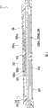
在本说明书中,诸如包含半导体存储器并用作用于存储各种类型的信息(例如数据、音频信号和视频信号)的信息媒介的IC存储卡的存储卡、具有除信息存储功能之外的功能(例如通信功能或接口功能)的卡式装置或PC卡、以及既具有信息存储功能又具有其它功能的卡式装置或PC卡通常被称为IC卡(集成电路卡)。包括邮票尺寸的卡的各种小且重量轻的IC卡最近已开发出来并投入到实际使用中。图20显示作为传统IC卡例子的IC卡的外观。In this specification, a memory card such as an IC memory card that includes a semiconductor memory and is used as an information medium for storing various types of information such as data, audio signals, and video signals, has a function other than an information storage function such as A card-type device or a PC card having a communication function or an interface function), and a card-type device or a PC card having both an information storage function and other functions are generally called IC cards (Integrated Circuit Cards). Various small and lightweight IC cards including stamp-sized cards have recently been developed and put into practical use. Fig. 20 shows the appearance of an IC card as an example of a conventional IC card.
图20中所示的IC存储卡1包括其内包含半导体存储器的存储卡本体2。用于将半导体存储器电连接到外部装置的外部连接端子5(5a-5i)被设置在存储卡本体2的下表面的一侧的边缘附近。外部装置的例子包括各种信息装置、视频装置和通信装置。另外,IC存储卡1包括用于防止在存储卡本体2的侧边缘处的错误删除的写保护开关9。在外部装置一侧对为物理开关的写保护开关9执行状态检测。更具体而言,用于检测写保护开关9的位置或状态的检测机构被设置在使用IC存储卡1的外部装置处或者用于将存储卡1连接到外部装置的连接器处。例如,在专利文件1中说明了这种类型的写保护开关9。An
也建议将写保护开关结合在存储卡本体内而非其侧边缘上。然而,因为存储卡尺寸小且薄,所以不得不以高精度将要组装在存储卡本体内的开关制造成小厚度。另外,当所组装的开关的高度大时,不得不通过在容纳在存储卡本体内的基板中设置通孔并将开关安装在通孔内来保证用于容纳开关的空间或高度。It is also recommended to incorporate the write-protect switch within the body of the memory card rather than on its side edge. However, since the memory card is small in size and thin, the switch to be assembled in the memory card body has to be manufactured in a small thickness with high precision. In addition, when the height of the assembled switch is large, a space or height for accommodating the switch has to be secured by providing a through hole in a substrate housed in the memory card body and mounting the switch in the through hole.
半导体元件集成水平的提高使得可以实现高容量IC存储卡或多功能卡式装置或PC卡。然而,目前所采用的一些装置不适用于这种高容量IC存储卡或多功能卡式装置,并且有时保证兼容性会成为问题。因此,IC卡向高容量及大量功能的发展正在推进,同时必须保证与具有有限容量或功能的目前可使用的装置的兼容性。An increase in the level of integration of semiconductor elements has made it possible to realize a high-capacity IC memory card or a multi-function card device or a PC card. However, currently used devices are not suitable for such high-capacity IC memory card or multi-function card type devices, and ensuring compatibility sometimes becomes a problem. Therefore, the development of IC cards toward high capacity and a large number of functions is advancing, and at the same time, it is necessary to ensure compatibility with currently available devices having limited capacities or functions.
专利文件1:日本专利申请公开出版物第2001-52135号Patent Document 1: Japanese Patent Application Publication No. 2001-52135
发明内容Contents of the invention
本发明所解决的问题Problems solved by the present invention
本发明的一个目的是提供一种小尺寸、薄、多功能的高容量IC卡,所述IC卡保证与具有有限容量或功能的目前可使用的装置的兼容性。An object of the present invention is to provide a small-sized, thin, multifunctional, high-capacity IC card that ensures compatibility with currently available devices having limited capacity or functions.
用于解决问题的方法method used to solve the problem
为了获得所述目的,本发明的IC卡包括具有至少两种操作模式的半导体元件、以及用于切换所述半导体元件的操作模式的物理开关。In order to achieve the object, an IC card of the present invention includes a semiconductor element having at least two operation modes, and a physical switch for switching the operation mode of the semiconductor element.
所述半导体元件的操作模式可以通过操纵所述物理开关进行切换。因此,如果两种或更多种操作模式中的任意一种操作模式被设定成有限存储容量或有限功能,则通过操纵所述物理开关可以保证用于具有有限容量或功能的外部装置。换句话说,如必要的话,通过操纵所述物理开关及切换操作模式可以保证与目前可使用的装置的兼容性。The operation mode of the semiconductor element can be switched by manipulating the physical switch. Therefore, if any one of two or more operation modes is set to a limited storage capacity or a limited function, it can be secured for an external device having a limited capacity or function by manipulating the physical switch. In other words, compatibility with currently available devices can be ensured by manipulating the physical switch and switching the operation mode, if necessary.
具体而言,所述物理开关可以被设定成至少两种状态,每一种状态对应于任意一种操作模式。所述半导体元件包括用于检测所述物理开关的状态并根据所检测的物理开关的状态切换操作模式的控制器。Specifically, the physical switch can be set to at least two states, and each state corresponds to any operation mode. The semiconductor element includes a controller for detecting a state of the physical switch and switching an operation mode according to the detected state of the physical switch.
更具体地,所述物理开关包括:多个电接触件,所述多个电接触件被设置在其上安装有所述半导体元件的基板上;可动式第一模制部件,所述可动式第一模制部件包括用于切换所述电接触件的电连接的接触端子;以及第二模制部件,所述第二模制部件将所述第一模制部件按压在设有所述电接触件的所述基板的表面上,从而保持所述接触端子与所述电接触件的接触压力,并且所述第二模制部件还用作容纳其上安装有所述半导体元件的所述基板的外部模制部件的一部分。More specifically, the physical switch includes: a plurality of electrical contacts disposed on a substrate on which the semiconductor element is mounted; a movable first molded part, the movable a movable first molded part comprising contact terminals for switching the electrical connection of said electrical contacts; and a second molded part pressing said first molded part against said first molded part on the surface of the substrate of the electrical contact, thereby maintaining the contact pressure of the contact terminal and the electrical contact, and the second molding part is also used to accommodate all the semiconductor elements mounted thereon. part of the outer molded part of the substrate described above.
因为通过从还用作所述外部模制部件的一部分的所述第二模制部件向所述第一模制部件施加压力保证了由所述接触端子施加到所述电接触件的接触压力,所以可以降低所述物理开关的高度。结果,不必使用需要精密加工的薄部件作为所述第一模制部件,并且不必执行所述基板的特定加工,例如通孔成形。因此,具有简单构造的用于切换操作模式的物理开关可以结合在所述IC卡中。换句话说,即使所述IC卡内已设置用于切换操作模式的所述物理开关,所述IC卡也可以小且薄。Since the contact pressure applied by the contact terminal to the electrical contact is ensured by applying pressure to the first molded part from the second molded part which also serves as a part of the outer molded part, So the height of the physical switch can be reduced. As a result, it is not necessary to use a thin part requiring precise processing as the first molded part, and it is not necessary to perform specific processing of the substrate, such as through-hole forming. Therefore, a physical switch for switching operation modes with a simple configuration can be incorporated in the IC card. In other words, even if the physical switch for switching operation modes is provided in the IC card, the IC card can be small and thin.
例如,所述物理开关的所述第一模制部件可以相对于所述基板和所述第二模制部件旋转。在这种布置中,仅需要执行旋转所述第一模制部件的操作以切换操作模式以及保证与目前可使用的装置的兼容性。可供选择地,所述物理开关的所述第一模制部件可以相对于所述基板和所述第二模制部件线性移动。在这种布置中,仅需要执行移动所述第一模制部件的操作以切换操作模式以及保证与目前可使用的装置的兼容性。For example, the first molded part of the physical switch may rotate relative to the base plate and the second molded part. In this arrangement, only the operation of rotating the first molded part needs to be performed to switch the mode of operation and to ensure compatibility with currently available devices. Alternatively, said first molded part of said physical switch is linearly movable relative to said base plate and said second molded part. In this arrangement, only the operation of moving the first molded part needs to be performed to switch the mode of operation and to ensure compatibility with currently available devices.
在用于电连接到外部装置的外部连接端子被设置在所述外部模制部件的一个边缘侧的情况下,所述物理开关优选地被设置在与设有所述外部连接端子的所述外部模制部件的边缘相对的另一边缘侧。通过将所述物理开关设置在这种位置处,使用者即使在所述IC卡的外部连接端子侧被插入到所述外部装置中时也可以看到所述物理开关。换句话说,使用者即使在所述IC卡已插入所述外部装置内之后在视觉上也可以识别出目前所设定的操作模式。In the case where an external connection terminal for electrical connection to an external device is provided on one edge side of the external molded part, the physical switch is preferably provided on the external part provided with the external connection terminal. The edge of the molded part is opposite the other edge side. By disposing the physical switch at such a position, the user can see the physical switch even when the external connection terminal side of the IC card is inserted into the external device. In other words, the user can visually recognize the currently set operation mode even after the IC card has been inserted into the external device.
所述半导体元件包括至少一个半导体存储器。所述半导体存储器具有多个信息存储区域,每一个信息存储区域被分配作为用于每种操作模式的可用区域。另外,所述控制器根据所检测的物理开关的状态指定作为可用区域的信息存储区域。The semiconductor component includes at least one semiconductor memory. The semiconductor memory has a plurality of information storage areas each allocated as an available area for each operation mode. In addition, the controller designates an information storage area as an available area according to the detected state of the physical switch.
如果关于所述多个操作模式中的任意一种操作模式可以使用的所述半导体存储器的信息存储区域中的一个区域的存储容量被设定为小于可用于其它操作模式的所述半导体存储器的其它信息存储区域的存储容量,则通过操纵所述物理开关来切换操作模式可以将所述IC卡的可用存储容量限制为其一部分。因此,通过操纵所述物理开关来切换操作模式,本发明的所述IC卡甚至可以用于不适用于具有高容量的信息存储区域的IC卡的外部装置。换句话说,通过操纵所述物理开关可以保证关于存储容量的相对于外部装置的标准的差异的兼容性。例如,所述半导体存储器为非易失性存储器(nonvolatile memory),例如快闪存储器。If the storage capacity of one of the information storage areas of the semiconductor memory usable with respect to any one of the plurality of operation modes is set to be smaller than the other of the semiconductor memory usable for other operation modes the storage capacity of the information storage area, the usable storage capacity of the IC card can be limited to a part thereof by manipulating the physical switch to switch the operation mode. Therefore, by manipulating the physical switch to switch the operation mode, the IC card of the present invention can be used even for an external device that is not suitable for an IC card having a high-capacity information storage area. In other words, compatibility with respect to differences in storage capacity with respect to standards of external devices can be secured by manipulating the physical switch. For example, the semiconductor memory is a nonvolatile memory, such as a flash memory.
所述半导体存储器的所述多个信息存储区域可以被格式化为对应于各文件系统的存储容量,每一个信息存储区域被分配为用于任意一种操作模式的可用区域。为了将所述IC卡用于对应于所述各文件系统的外部装置,仅需要操纵所述物理开关来切换操作模式。例如,因为所述多个信息存储区域对应于各个文件系统,所以通过操纵所述物理开关可以相对于文件系统中的差异保证与外部装置的兼容性。The plurality of information storage areas of the semiconductor memory may be formatted to correspond to storage capacities of respective file systems, each information storage area being allocated as an available area for any one operation mode. In order to use the IC card for external devices corresponding to the respective file systems, it is only necessary to manipulate the physical switch to switch the operation mode. For example, since the plurality of information storage areas correspond to respective file systems, compatibility with external devices can be secured against differences in file systems by manipulating the physical switches.
可供选择地,所述半导体元件包括半导体存储器和用于执行除信息存储之外的功能的另外的半导体元件,所述半导体存储器和所述另外的半导体元件中的任意一个或两者被分配为各操作模式,其中控制器根据所检测的物理开关的状态激活所述半导体存储器和另外的半导体元件中的任意一个或两者。为了指定信息存储功能和除信息存储功能之外的功能,例如通信功能、接口功能、安全功能和电子货币功能,仅需要通过操纵所述物理开关来切换操作模式。如果与其它操作模式中的功能相比,限制多个操作模式中的任意一种模式中的可执行功能,则通过操纵所述物理开关以切换操作模式可将所述IC卡可执行的功能限定为所述多个功能中的某些功能。这会保证本发明的所述IC卡可以用于具有限制功能的现有外部装置。换句话说,通过操纵所述物理开关可以保证关于外部装置的功能差异方面的兼容性。Alternatively, the semiconductor element includes a semiconductor memory and another semiconductor element for performing functions other than information storage, either or both of the semiconductor memory and the other semiconductor element are assigned as Modes of operation in which the controller activates either or both of the semiconductor memory and the further semiconductor element depending on the detected state of the physical switch. In order to designate the information storage function and functions other than the information storage function, such as communication function, interface function, security function, and electronic money function, it is only necessary to switch the operation mode by manipulating the physical switch. If executable functions in any one of a plurality of operation modes are restricted compared with functions in other operation modes, the functions executable by the IC card can be limited by manipulating the physical switch to switch the operation mode for some of the plurality of functions. This will ensure that the IC card of the present invention can be used with existing external devices having limited functions. In other words, compatibility with respect to functional differences of external devices can be secured by manipulating the physical switch.
本发明的效果Effect of the present invention
具有用于切换操作模式的所述物理开关的本发明的所述IC卡获得增加的容量和多功能性,以及与具有有限容量或功能的现有外部装置的兼容性。另外,因为所述外部模制部件的一部分用作所述物理开关的一部分,所以即使用于切换操作模式的所述物理开关被设置在所述IC卡内也可以减小所述IC卡的尺寸和厚度。The IC card of the present invention having the physical switch for switching operation modes achieves increased capacity and versatility, and compatibility with existing external devices having limited capacity or functions. In addition, since a part of the external molding part is used as a part of the physical switch, the size of the IC card can be reduced even if the physical switch for switching operation modes is provided in the IC card and thickness.
附图说明Description of drawings
图1是本发明的第一实施例的IC存储卡的下侧视图;Fig. 1 is the lower side view of the IC memory card of the first embodiment of the present invention;
图2是本发明的第一实施例的IC存储卡的上侧视图;Fig. 2 is the upper side view of the IC memory card of the first embodiment of the present invention;
图3是沿着图1中的线III-III的示意性放大横截面图;Fig. 3 is a schematic enlarged cross-sectional view along line III-III in Fig. 1;
图4是本发明的第一实施例的IC存储卡的分解透视图;4 is an exploded perspective view of the IC memory card of the first embodiment of the present invention;
图5是自本发明的第一实施例的IC存储卡的下侧的透视图;Fig. 5 is the perspective view from the lower side of the IC memory card of the first embodiment of the present invention;
图6A是自本发明的第一实施例的IC存储卡的下侧的部分透视图,其中模式转变开关被设定为开关状态1;6A is a partial perspective view from the lower side of the IC memory card of the first embodiment of the present invention, wherein the mode changeover switch is set to switch
图6B是自本发明的第一实施例的IC存储卡的下侧的部分透视图,其中模式转变开关被设定为开关状态3;6B is a partial perspective view from the lower side of the IC memory card of the first embodiment of the present invention, wherein the mode changeover switch is set to switch state 3;
图7是说明本发明的第一实施例的IC存储卡的示意结构的方块图;7 is a block diagram illustrating a schematic structure of an IC memory card of a first embodiment of the present invention;
图8说明下部壳体的内表面侧;Figure 8 illustrates the inner surface side of the lower housing;
图9说明上部壳体的内表面侧;Figure 9 illustrates the inner surface side of the upper housing;
图10A是旋转部件的平面图;Figure 10A is a plan view of a rotating part;
图10B是说明从图10A中的箭头X所观察的旋转部件的视图;FIG. 10B is a view illustrating a rotating member viewed from an arrow X in FIG. 10A;
图11是说明本发明的第二实施例的IC存储卡的示意结构的方块图;11 is a block diagram illustrating a schematic structure of an IC memory card of a second embodiment of the present invention;
图12是说明本发明的第三实施例的IC卡的示意结构的方块图;12 is a block diagram illustrating a schematic structure of an IC card of a third embodiment of the present invention;
图13是本发明的第四实施例的IC卡的下侧视图;Fig. 13 is the lower side view of the IC card of the fourth embodiment of the present invention;
图14是沿着图13中的线XIV-XIV的示意性横截面图;Fig. 14 is a schematic cross-sectional view along line XIV-XIV in Fig. 13;
图15是本发明的第四实施例的IC卡的分解透视图;15 is an exploded perspective view of an IC card of a fourth embodiment of the present invention;
图16是从本发明的第四实施例的IC存储卡的下侧所观察的透视图;16 is a perspective view seen from the lower side of an IC memory card of a fourth embodiment of the present invention;
图17A是从本发明的第四实施例的IC存储卡的下侧所观察的部分透视图,其中模式转变开关被设定为开关状态1;17A is a partial perspective view viewed from the lower side of the IC memory card of the fourth embodiment of the present invention, wherein the mode changeover switch is set to switch
图17B是从本发明的第四实施例的IC存储卡的下侧所观察的部分透视图,其中模式转变开关被设定为开关状态3;17B is a partial perspective view viewed from the lower side of the IC memory card of the fourth embodiment of the present invention, wherein the mode changeover switch is set to switch state 3;
图18说明下部壳体的内表面侧;Figure 18 illustrates the inner surface side of the lower housing;
图19A是滑动部件的平面图;Fig. 19A is a plan view of a sliding part;
图19B是说明从图19A中的箭头XIX所观察的滑动部件的视图;FIG. 19B is a view illustrating a sliding member viewed from arrow XIX in FIG. 19A;
图19C是说明从图19A中的箭头XIX'所观察的滑动部件的视图;以及Fig. 19C is a view illustrating the sliding member viewed from arrow XIX' in Fig. 19A; and
图20是传统的IC存储卡的下侧视图。Fig. 20 is a lower side view of a conventional IC memory card.
附图标记说明Explanation of reference signs
11:IC存储卡11: IC memory card
12:下部壳体12: Lower shell
13:上部壳体13: Upper shell
14:壳体14: Shell
15:外部装置15: External device
17a-17i:外部连接端子17a-17i: External connection terminals
18:模式转变开关18: Mode change switch
19:写保护开关19: Write protection switch
20:基板20: Substrate
21,22:突起21, 22: protrusion
23a-23h:端子开口23a-23h: Terminal opening
24:控制器LSI24: Controller LSI
25A,25B:半导体存储器25A, 25B: semiconductor memory
26:半导体元件26: Semiconductor components
27a-27c,28,29:端子27a-27c, 28, 29: terminals
31a-31d:电接触件31a-31d: electrical contacts
32:接触端子32: Contact terminal
33:旋转部件33: Rotating parts
34a-34d:弹性件34a-34d: Elastic parts
35a-35d:接触部35a-35d: contact part
36:基部36: Base
37:保持部37: Keeping Department
38:定位突起38: positioning protrusion
39:轴承孔39: Bearing hole
40:圆弧形孔40: circular arc hole
42:容纳凹入部42: Accommodating recess
43:轴部43: Shaft
44:通孔44: Through hole
45:凹入部45: concave part
46:开口46: opening
48:凹口48: notch
51A,51B,51C:半导体存储器51A, 51B, 51C: semiconductor memory
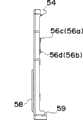
53:IC卡53: IC card
54:另一半导体存储器54: Another semiconductor memory
51:模式转变开关51: Mode change switch
52a-52d:电接触件52a-52d: electrical contacts
53:接触端子53: contact terminal
54:滑动部件54: sliding parts
55a-55d:弹性件55a-55d: Elastic parts
56a-56d:接触部56a-56d: contact part
57:基部57: base
58:保持部58: Keeping Department
59:突出部59: protrusion
61:定位突起61: positioning protrusion
62a,62b:矩形孔62a, 62b: rectangular holes
63:容纳凹入部63: Accommodating recess
64:窗孔64: window hole
65a-65c:凹口65a-65c: Notches
具体实施方式Detailed ways
第一实施例first embodiment
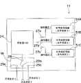
图1至图7显示本发明的第一实施例的IC存储卡(IC卡)11。如图3和图4中所示,IC存储卡11具有包括连接在一起的下部壳体(第二模制部件)12和上部壳体13的壳体(外部模制部件)14。下部壳体12和上部壳体13均由树脂模制。参照图1和图2,用于电连接到外部装置15的外部连接端子17(包括用于连接外部装置15和IC存储卡11的连接器)被设置在壳体14的下部壳体12的一个边缘附近。外部装置15的例子包括各种信息装置、视频装置和通信装置,包括小型便携式装置。在本发明中有九个外部连接端子17a至17i。在所述外部连接端子17a至17i中,外部连接端子17a、17b、17h和17i用于与外部装置15交换数据或信息,外部连接端子17c和17f用于从外部装置15接收时钟信号或指令,外部连接端子17d和17f用于从外部装置15供应电力。用于切换下述操作模式的模式转变开关(物理开关)18被设置在与设有外部连接端子17的边缘相对的壳体14的下部壳体12的另一边缘附近。用于防止错误删除的写保护开关19被设置在壳体14的右侧边缘上(图1)。1 to 7 show an IC memory card (IC card) 11 of a first embodiment of the present invention. As shown in FIGS. 3 and 4 , the
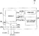
参照图3、图4和图5,基板20和模式转变开关18的旋转部件33被容纳在壳体14中。如图8中所示,用于定位基板20的一对突起21被设置在下部壳体12的内表面上。如图9中所示,用于定位基板20的突起22被设置在上部壳体13的内表面上。Referring to FIGS. 3 , 4 and 5 , the
参照图4和图5,在位于下部壳体12一侧的基板20的表面上,前述的外部连接端子17a至17i被设置在一个边缘附近。端子开口23a至23h在下部壳体12的一个边缘附近被设置在对应于外部连接端子17a至17i的位置处(亦见图8)。外部连接端子17a至17i从端子开口23a至23h暴露出来。另外,在位于下部壳体12一侧的基板20的表面上,模式转变开关18的电接触件31a至31d被设置在与外部连接端子17a至17i相对的边缘附近。4 and 5, on the surface of the
如图3、图4和图7中所示,各种半导体元件被安装在基板20上。具体而言,控制器LSI(控制器)24以及为非易失性存储器(例如快闪存储器)的半导体存储器25A和25B被安装在与设有外部连接端子17a至17i和电接触件31a至31d的侧面相对的基板20的表面上。在本实施例中,一个半导体存储器25A的信息存储区域的容量为2千兆字节,而另一半导体存储器25B的信息存储区域的容量为6千兆字节。另外,根据缘于电路配置的需求,具有除信息存储功能之外的功能的其它芯片部件或半导体元件26也可以安装在基板20上。此外,用于电连接外部连接端子17、电接触件31a至31d、控制器LSI 24、半导体存储器25A和25B以及其它半导体元件26的导电路径(图式中未示出)形成于基板20上。As shown in FIGS. 3 , 4 and 7 , various semiconductor elements are mounted on the
控制器LSI 24控制IC存储卡11的整体操作。具体而言,控制器LSI 24执行的操作涉及从外部装置15接收数据和各种类型的信息(例如音频信号和视频信号)、将数据或信息写入半导体存储器25A和25B、从半导体存储器25A和25B读取数据或信息、以及将数据或信息传输到外部装置15。The
本实施例的IC存储卡11具有涉及控制器LSI 24以及半导体存储器25A和25B的操作和功能的三种模式(操作模式)。这三种操作模式在下文将被称为“操作模式1”、“操作模式2”和“操作模式3”。如下文中所述,IC存储卡11的操作模式通过操纵模式转变开关18可以被设定成“操作模式1”、“操作模式2”和“操作模式3”中的任意一种模式。The
“操作模式1”为仅有2千兆字节的半导体存储器25A作为控制器LSI 24的控制目标的操作模式。换句话说,“操作模式1”中的IC存储卡11的存储容量为2千兆字节。在图7中所示的示意方块图中,控制器LSI 24连接到端子27a的状态对应于“操作模式1”。"
“操作模式2”为2千兆字节的半导体存储器25A和6千兆字节的半导体存储器25B均为控制器LSI 24的控制目标的操作模式。换句话说,“操作模式2”中的IC存储卡11的存储容量为8千兆字节。在图7中,控制器LSI 24连接到端子27b的状态对应于“操作模式2”。The "
“操作模式3”为仅有6千兆字节的半导体存储器25B为控制器LSI 24的控制目标的操作模式。换句话说,“操作模式3”中的IC存储卡11的存储容量为6千兆字节。在图7中,控制器LSI 24连接到端子27c的状态对应于“操作模式3”。"Operation mode 3" is an operation mode in which only the
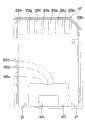
下面将说明模式转变开关18。在本实施例中,模式转变开关18为旋转开关。参照图3至图5,模式转变开关18包括设置在与设有外部连接端子17的表面相同的基板20的表面上的四个电接触件31a至31d以及旋转部件(第一模制部件)33,其中用于切换电接触件31a至31d的电连接的接触端子32连接到所述旋转部件。通过对树脂进行模制获得旋转部件33。另外,如稍后所述,壳体14的下部壳体12也用作模式转变开关18的一部分。如图3和图4中最清楚地示出,旋转部件33被设置在下部壳体12与基板20之间。The
还参照图10A和图10B,接触端子32包括为圆弧形式的四个弹性件34a至34d。接触部35a至35d被设置在各弹性件34a至34d的远端上。另一方面,弹性件34a至34d的近侧通过共用基部36互相连接。Referring also to FIGS. 10A and 10B , the
在图10A中,旋转部件33包括位于下侧部的保持部37。保持部37的外边缘为圆弧形状并具有形成于其上的用于防止滑脱的连续重复的小突起。另外,旋转部件33包括在与保持部37相对的一部分处向外突出的定位突起38。作为沿厚度方向穿透的圆孔的轴承孔39形成于旋转部件33的中心部分处。另外,在旋转部件33中,一对圆弧形孔40a、40b形成为在轴承孔39的两侧沿厚度方向穿透。在旋转部件33中模制接触端子32的基部36,从而将接触端子32固定到旋转部件33。接触端子32的弹性件34a和34b突出到一个圆弧形孔40a内,而弹性件34c和34d突出到另一圆弧形孔40b内。In FIG. 10A , the rotating
还参照图8,具有与旋转部件33相似的轮廓的容纳凹入部42形成于与端子开口23a至23h相对的下部壳体12的内表面的边缘附近。旋转部件33被容纳在容纳凹入部42内。圆柱形轴部43从容纳凹入部42的底面突出。轴部43通过容纳在容纳凹入部42内的旋转部件33的轴承孔39。因此,旋转部件33可以在容纳凹入部42内绕着轴部43相对于基板20和壳体14旋转。轴部43延伸通过基板20的通孔44(图4中所示),到达上部壳体13的内表面。在图5中,两个电接触件31a、31b被定位在轴部43的左侧,而其余两个电接触件31c、31d被定位在右侧。Referring also to FIG. 8 , an
如图1、图4和图5中所示,凹入部45形成于下部壳体12的外表面的与端子开口23a至23h相对的边缘中。另外,使凹入部45与容纳凹入部42相连通的开口46(见图4)被设置在下部壳体12中。如图1中最清楚地示出,容纳在容纳凹入部42内的旋转部件33的保持部37的一部分通过开口46暴露到壳体14外。因此,使用者通过操纵保持部37可以绕着轴部43旋转旋转部件33。As shown in FIGS. 1 , 4 and 5 , recessed
如上所述,旋转部件33被设置在下部壳体12与基板20之间。下部壳体12与基板20之间的空间,更具体地,容纳凹入部42的下表面与基板20之间的空间大致限制到旋转部件33的厚度。因此,下部壳体12朝着基板20按压或推动旋转部件33。下部壳体12的这种推动动作保证固定到旋转部件33的接触端子32的接触部35a至35b与电接触件31a至31d之间的接触压力。因而,作为壳体14的一部分的下部壳体12推动旋转部件33保证接触端子32与电接触件31a至31d之间的接触压力。因此,可以减小模式转变开关18的高度。这使得旋转部件33不必要为需要精确加工的薄部件,并且不需要对基板20进行特定的加工,例如形成用于布置旋转部件33的通孔。因而,模式转变开关18可以通过简单布置结合在IC存储卡11内。换句话说,即使IC存储卡11内设有模式转变开关18,IC存储卡11也很薄且尺寸小。As described above, the rotating
参照图5和图8,凹口48a至48c形成于容纳凹入部42的圆周壁的一部分中。旋转部件33的定位突起38与凹口48a至48c相接合,从而确定旋转部件33绕着轴部43的旋转角位置。旋转部件33可以被设定到三个角位置。具体而言,旋转部件33可以被设定到如图6A中所示使定位突起38与右侧凹口48c接合的旋转角位置、如图5中所示使定位突起38与中央凹口48b接合的旋转角位置、以及如图6B中所示使定位突起38与左侧凹口48a接合的旋转角位置。模式转变开关18的旋转部件33设定到图6A、图5和图6B中所示的旋转角位置的状态分别被称为“开关状态1”、“开关状态2”和“开关状态3”。Referring to FIGS. 5 and 8 , notches 48 a to 48 c are formed in a part of the circumferential wall of the
在图6A中所示的“开关状态1”中,位于旋转部件33上的接触端子32的接触部35a和35b与位于基板20上的电接触件31a和31b相接触。结果,电接触件31a和31b通过接触端子32电短路或电连接。另一方面,电接触件31c和31d未与接触端子32接触且被电绝缘。在图7中所示的示意方块图中,端子28(对应于电接触件31a至31d)连接到端子29a的状态等效于模式转变开关18的“开关状态1”。In “
在图5中所示的“开关状态2”中,位于旋转部件33上的接触端子32未与位于基板20上的四个电接触件31a至31d中的任何一个接触。因此,电接触件31a和31b电绝缘,另外电接触件31c和31d也电绝缘。图7中端子28连接到端子29b的状态等效于模式转变开关18的“开关状态2”。In “switching
在图6B中所示的“开关状态3”中,位于旋转部件33上的接触端子32的接触部35c和35d与位于基板20上的电接触件31c和31d相接触。因此,电接触件31c和31d通过接触端子32电连接。另一方面,电接触件31a和31b未与接触端子32相接触且互相电绝缘。图7中端子28连接到端子29c的状态等效于模式转变开关18的“开关状态3”。In “Switching State 3 ” shown in FIG. 6B , the
在本实施例中,模式转变开关18的“开关状态1”、“开关状态2”和“开关状态3”分别对应于“操作模式1”、“操作模式2”和“操作模式3”,并且控制器LSI 24储存这种对应关系。如上所述,四个电接触件31a至31d的连接和绝缘关系在“开关状态1”、“开关状态2”和“开关状态3”中是不同的。因此,控制器LSI 24通过将电压施加到电接触件31a至31d可以检测模式转变开关18被设定到“开关状态1”、“开关状态2”和“开关状态3”中的哪一种状态。控制器LSI 24可以根据检测的模式转变开关18的状态执行“操作模式1”、“操作模式2”和“操作模式3”中的任意一种模式。In the present embodiment, "switch
如果模式转变开关18处于图6A中所示的“开关状态1”(在图7中为端子28连接到端子29a的状态),则控制器LSI 24会检测到这种状态。另外,已检测到“开关状态1”的控制器LSI 24执行对应于“开关状态1”的“操作模式1”,并且仅有2千兆字节的半导体存储器25A变为控制器LSI 24的控制目标(在图7中为控制器LSI 24连接到端子27a的状态)。另外,如果模式转变开关18处于图5中所示的“开关状态2”(在图7中为端子28连接到端子29b的状态),则已检测到这种状态的控制器LSI 24执行对应于“开关状态2”的“操作模式2”。这意味着2千兆字节的半导体存储器25A和6千兆字节的半导体存储器25B(即,为8千兆字节信息存储容量)均变为控制器LSI 24的控制目标。如果模式转变开关18处于图6B中所示的“开关状态3”(在图7中为端子28连接到端子29c的状态),则已检测到这种状态的控制器LSI 24执行对应于“开关状态3”的“操作模式3”。这意味着仅有6千兆字节的半导体存储器25B变为控制器LSI 24的控制目标(在图7中为控制器LSI 24连接到端子27C的状态)。If the
在本实施例的IC存储卡11中,可以通过操纵模式转变开关18变换操作模式来切换作为控制器LSI 24的控制目标的信息存储区域的存储容量。因此,IC卡可以用于适于高容量IC卡的外部装置15和仅适于低容量IC卡的外部装置15。换句话说,本实施例的IC存储卡11关于涉及存储容量的外部装置15的标准之间的差异具有兼容性。例如,在用于适于具有相对较高的容量(即,6千兆字节或8千兆字节的存储容量)的IC存储卡的外部装置15中,模式转变开关18可以被设定成“开关状态1”或“开关状态2”,使得作为控制器LSI 24的控制目标的信息存储区域的存储容量被设定成6千兆字节或8千兆字节。另一方面,在用于仅适于具有相对较低的容量(即,2千兆字节的存储容量)的IC存储卡的外部装置15中,模式转变开关18可以被设定成“开关状态3”,使得作为控制器LSI 24的控制目标的信息存储区域的存储容量被设定成2千兆字节。In the
如上所述,模式转变开关18被设置在与设有外部连接端子17的另一边缘相对的壳体边缘附近。因此,如通过参照图1可看出,即使IC存储卡11已插入外部装置15内,使用者也可以看到模式转变开关18。换句话说,使用者在视觉上容易识别模式转变开关18已被设定成“开关状态1”、“开关状态2”和“开关状态3”中的哪一种状态,即,目前对IC存储卡11所设定的操作模式是否是“操作模式1”、“操作模式2”或“操作模式3”。特别是,如果表示目前操作模式的标记(例如数字、字母或颜色符号)被设置在模式转变开关18的保持部37的侧面上或者在所述侧面附近,则即使IC存储卡11已插入外部装置15内,在视觉上也容易识别IC存储卡11目前被设定的操作模式。As described above, the
第二实施例second embodiment
除了格式化为对应于互不相同的文件系统A、B和C的存储容量的半导体存储器51A、51B和51C安装在基板20上之外(例如,见图4),图11中所示的本发明的第二实施例的IC存储卡11的结构与第一实施例的IC存储卡11的结构相同。在图11中,与第一实施例相同的元件被指定相同的附图标记。另外,图11中未示出的本实施例的IC存储卡11的结构与参照图1至图6B和图8至图10B已说明的结构相同。本实施例与第一实施例的相同之处还在于,图6A中所示的“开关状态1”、图5中所示的“开关状态2”和图6B中所示的“开关状态3”分别对应于“操作模式1”、“操作模式2”和“操作模式3”,并且控制器LSI 24检测开关状态并执行对应于所检测的开关状态的操作模式。然而,本实施例中的操作模式不同于第一实施例的操作模式。Except that
在“操作模式1”中,仅有已格式化为对应于文件系统A的存储容量的半导体存储器51A为控制器LSI 24的控制目标,以用于例如信息读取或写入的操作。在“操作模式2”中,仅有已格式化为对应于文件系统B的存储容量的半导体存储器51B为控制器LSI 24的控制目标。在“操作模式3”中,仅有已格式化为对应于文件系统C的存储容量的半导体存储器51C为控制器LSI 24的控制目标。In "
通过操纵模式转变开关18变换操作模式来切换操作模式可以将本实施例的IC存储卡11用于采用三种不同类型的文件系统A、B和C的外部装置15。换句话说,通过操纵模式转变开关18可以保证关于外部装置15的文件系统的差异的兼容性。文件系统A、B和C不需要彼此完全不同,它们可以为部分或完全相同的文件系统,只要控制器LSI 24的控制目标可以被独立处理即可。Switching the operation mode by manipulating the
第三实施例third embodiment
除了将半导体存储器53和不同于半导体存储器并且具有除信息存储功能之外的功能(如通信功能、接口功能、安全功能和电子货币功能)的半导体元件54安装在基板20上之外,图12中所示的本发明的第三实施例的IC卡52的结构与第一实施例的IC存储卡11的结构相同。在图12中,与第一实施例相同的元件被分配相同的附图标记。另外,图12中未示出的本实施例的IC存储卡52的结构与参照图1至图6B和图8至图10B已说明的结构相同。本实施例与第一实施例的相同之处还在于,图6A中所示的“开关状态1”、图5中所示的“开关状态2”和图6B中所示的“开关状态3”分别对应于“操作模式1”、“操作模式2”和“操作模式3”,并且控制器LSI 24检测开关状态并执行对应于所检测的开关状态的操作模式。然而,本实施例中的操作模式不同于第一实施例的操作模式。In addition to mounting a
在“操作模式1”中,仅有半导体存储器53作为控制器LSI 24的控制目标,用于例如信息读取或写入的操作。在“操作模式2”中,半导体存储器53和不同于所述半导体存储器的半导体元件54作为控制器LSI 24的控制目标。因此,在“操作模式2”中,关于半导体存储器53的功能(例如读取及写入各种类型的数据或信息)以及半导体元件54的功能(例如通信功能或接口功能)两者均可被执行。另外,在“操作模式3”中,仅有不同于所述半导体存储器的半导体元件54作为控制器LSI 24的控制目标,因此仅可以执行半导体元件54的功能,例如通信功能或接口功能。In "
通过操纵模式转变开关18变换操作模式可以限定可以由IC卡52执行的功能,以用于仅对应于这种限制功能的外部装置15。换句话说,通过操纵模式转变开关18可以保证关于外部装置15的功能差异的兼容性。例如,当外部装置15对应于具有信息存储功能的IC卡但不对应于具有通信功能或接口功能的IC卡时,通过将模式转变开关18设定成“开关状态1”以获得“操作模式1”,可以将本实施例的IC卡52用于这种外部装置15。同样,当外部装置15对应于具有通信功能或接口功能的IC卡但不对应于具有信息存储功能的IC卡时,通过将模式转变开关18设定成“开关状态3”以获得“操作模式3”,可以将本实施例的IC卡52用于这种外部装置15。Changing the operation mode by manipulating the
第四实施例Fourth embodiment
图13至图17B显示本发明的第四实施例的IC存储卡11。13 to 17B show an
本实施例的模式转变开关51为滑动开关。参照图14至图16,模式转变开关51包括设置在与设有外部连接端子17a至17i的表面相同的基板20的表面上的四个电接触件52a至52d以及滑动部件(第一模制部件)54,其中用于切换电接触件52a至52d的电连接的接触端子53被连接到所述滑动部件。由树脂模制成滑动部件54。另外,壳体14的下部壳体12也用作模式转变开关51的一部分。如图14和图15中最清楚地示出,滑动部件54被设置在下部壳体12与基板20之间。The
还参照图19A至图19C,接触端子53包括四个直的或线性的弹性件55a至55d。接触部56a至56d被设置在各弹性件55a至55d的远端上。另一方面,弹性件55a至55d的近侧通过共用基部57互相连接。Referring also to FIGS. 19A to 19C, the
如图19A中所示,滑动部件54包括在下侧的位于上表面上的保持部58。另外,如图19C中所示,沿着下侧边缘延伸的突起61被设置在滑动部件54的下表面上。此外,滑动部件54包括在与保持部58相对的位置处向外突出的定位突起61。在滑动部件54中,一对对称布置的矩形孔62a和62b形成为沿厚度方向穿透。在滑动部件54中模制出接触端子53的基部57。接触端子53的弹性件55a和55b突出到一个矩形孔62a内,而弹性件55c和55b突出到另一矩形孔62b内。As shown in FIG. 19A , the
还参照图18,具有与滑动部件54相似的外轮廓的容纳凹入部63形成于与端子开口23a和23h相对的下部壳体12的内表面的边缘附近。滑动部件54被容纳在容纳凹入部63内,并且可以在容纳凹入部63内相对于基板20和壳体14线性移动。使下部壳体12的内部与外部相连通的窗孔64形成于容纳凹入部63的下表面中。如图13中所示,包括保持部58的滑动部件54的一部分通过窗孔64暴露到壳体14外。因此,使用者通过操纵保持部58可以线性移动滑动部件54。Referring also to FIG. 18 , accommodating recessed
如上所述,滑动部件54被设置在下部壳体12与基板20之间。参照图16,滑动部件54的下边缘从基板20的边缘突出,并且突出部59的末端邻接上部壳体13的内表面。因为容纳凹入部63的下表面与基板20之间的空间大致限制为滑动部件54的除突出部59之外的厚度,所以下部壳体12朝着基板20按压或推动滑动部件54。下部壳体12的这种推动动作保证固定到滑动部件54的接触端子53的接触部56a至56d与电接触件52a至52d之间的接触压力。因而,用作为壳体14的一部分的下部壳体12推动滑动部件54保证了接触端子53与电接触件52a至52d之间的接触压力。因此,滑动部件54不必要为需要精确加工的薄部件,并且不需要对基板20进行特定的加工,例如形成用于布置滑动部件54的通孔。因而,模式转变开关51可以通过简单布置结合在IC存储卡11内。因此,这个实施例的IC存储卡11薄且尺寸小。As described above, the
参照图16至图18,凹口65a至65c形成于容纳凹入部63的圆周壁的一部分中。滑动部件54的定位突起61与凹口65a至65c相接合,从而获得对滑动部件54的位置的确定。滑动部件54可以被设定到三个位置处。具体而言,滑动部件54可以被设定到如图17A中所示使定位突起61与左侧凹口65a接合的位置(开关状态1)、如图16中所示使定位突起61与中央凹口65b接合的位置(开关状态2)、以及如图17B中所示使定位突起61与右侧凹口65c接合的位置(开关状态3)。Referring to FIGS. 16 to 18 ,
在图17A中所示的“开关状态1”中,位于滑动部件54上的接触端子53的接触部56a和56b与位于基板20上的电接触件52a和52b相接触。因此,电接触件52a和52b通过接触端子53电短路或电连接。另一方面,电接触件52c和52d未与接触端子53接触,并且电绝缘。在图16中所示的“开关状态2”中,位于滑动部件54上的接触端子53未与位于基板20上的四个电接触件52a至52d中的任何一个接触。因此,电接触件52a和52b电绝缘,并且电接触件52c和52d电绝缘。在图17B中所示的“开关状态3”中,位于滑动部件54上的接触端子53的接触部56c和56d与位于基板20上的电接触件52c和52d相接触。因此,电接触件52c和52d通过接触端子53电连接。另一方面,电接触件52a和52b未与接触端子53相接触且互相电绝缘。In "
如上所述,四个电接触件52a至52d的连接和绝缘关系在“开关状态1”、“开关状态2”和“开关状态3”中是不同的。因此,控制器LSI 24通过将电压施加到电接触件52a至52d可以检测模式转变开关18被设定到“开关状态1”、“开关状态2”和“开关状态3”中的哪一种状态,并且可以根据检测结果执行“操作模式1”、“操作模式2”和“操作模式3”中的任意一种模式。As described above, the connection and insulation relations of the four
由于第四实施例的其它特征和操作与第一实施例的特征和操作相同,因此相同的元件被指定相同的附图标记,并且省略对所述元件的详细说明。本实施例的滑动式模式转变开关51还可以应用在第二实施例的IC存储卡11或第三实施例的IC卡52中。Since other features and operations of the fourth embodiment are the same as those of the first embodiment, the same elements are assigned the same reference numerals, and detailed descriptions of the elements are omitted. The sliding
本发明不限于上述实施例且可以以各种方式变化。模式转变开关的机械结构不限于实施例的机械结构,只要模式转变开关可以设定在多个位置或状态即可。另外,可以对一个半导体存储器设定多个信息存储区域,并且可以根据模式转变开关的状态切换将作为控制器LSI的控制目标的信息存储区域。此外,模式转变开关的开关状态和对应于所述开关状态的操作模式的数量不限于3而可以为2或4及更多。The present invention is not limited to the above-described embodiments and can be varied in various ways. The mechanical structure of the mode change switch is not limited to that of the embodiment as long as the mode change switch can be set in multiple positions or states. In addition, a plurality of information storage areas can be set to one semiconductor memory, and an information storage area to be a control target of the controller LSI can be switched according to the state of the mode change switch. In addition, the switch state of the mode changeover switch and the number of operation modes corresponding to the switch state are not limited to 3 but may be 2 or 4 and more.
工业适用性Industrial applicability
尽管本发明的IC卡具有高容量且是多功能的,所述IC卡通过操纵模式转变开关切换操作模式来限制一部分信息存储容量或功能也可以获得与现有装置的兼容性。另外,因为通过操纵模式转变开关来执行操作模式的切换,所以使用者在视觉上容易识别操作模式。结果,本发明的IC卡适于作为IC存储卡,所述IC存储卡具有可以用作小型便携式装置中的用于存储信息(例如数据或音频信号)的媒介的半导体存储器,以及用作具有除信息存储功能之外的功能(例如,通信功能或接口功能)的IC卡、以及用作具有信息存储功能和其它功能的IC卡。Although the IC card of the present invention has a high capacity and is multifunctional, the IC card can obtain compatibility with existing devices by limiting a part of information storage capacity or functions by manipulating a mode changeover switch to switch operation modes. In addition, since switching of the operation mode is performed by manipulating the mode changeover switch, it is easy for the user to visually recognize the operation mode. As a result, the IC card of the present invention is suitable as an IC memory card having a semiconductor memory usable as a medium for storing information such as data or audio signals in a small portable IC cards with functions other than the information storage function (for example, a communication function or an interface function), and IC cards used as having an information storage function and other functions.
Claims (9)
Applications Claiming Priority (3)
| Application Number | Priority Date | Filing Date | Title |
|---|---|---|---|
| JP2004181039 | 2004-06-18 | ||
| JP181039/2004 | 2004-06-18 | ||
| PCT/JP2005/011149WO2005124670A1 (en) | 2004-06-18 | 2005-06-17 | Ic card |
Publications (2)
| Publication Number | Publication Date |
|---|---|
| CN101014969A CN101014969A (en) | 2007-08-08 |
| CN101014969Btrue CN101014969B (en) | 2011-03-30 |
Family
ID=35509923
Family Applications (1)
| Application Number | Title | Priority Date | Filing Date |
|---|---|---|---|
| CN2005800205994AExpired - Fee RelatedCN101014969B (en) | 2004-06-18 | 2005-06-17 | IC card |
Country Status (5)
| Country | Link |
|---|---|
| US (1) | US7616447B2 (en) |
| JP (1) | JPWO2005124670A1 (en) |
| CN (1) | CN101014969B (en) |
| TW (1) | TW200606731A (en) |
| WO (1) | WO2005124670A1 (en) |
Families Citing this family (21)
| Publication number | Priority date | Publication date | Assignee | Title |
|---|---|---|---|---|
| US7830666B2 (en)* | 2000-01-06 | 2010-11-09 | Super Talent Electronics, Inc. | Manufacturing process for single-chip MMC/SD flash memory device with molded asymmetric circuit board |
| US7872871B2 (en)* | 2000-01-06 | 2011-01-18 | Super Talent Electronics, Inc. | Molding methods to manufacture single-chip chip-on-board USB device |
| US8998620B2 (en)* | 2003-12-02 | 2015-04-07 | Super Talent Technology, Corp. | Molding method for COB-EUSB devices and metal housing package |
| US8102657B2 (en) | 2003-12-02 | 2012-01-24 | Super Talent Electronics, Inc. | Single shot molding method for COB USB/EUSB devices with contact pad ribs |
| JP2008108299A (en)* | 2006-10-23 | 2008-05-08 | Toshiba Corp | Nonvolatile semiconductor memory and memory card |
| GB2450355A (en)* | 2007-06-20 | 2008-12-24 | Samsung Electronics Co Ltd | Re-configurable memory cards having multiple application based functions of operating, and methods of forming the same |
| US20090094678A1 (en)* | 2007-10-05 | 2009-04-09 | Nokia Corporation | Mulimode device |
| JP2009157628A (en)* | 2007-12-26 | 2009-07-16 | Toshiba Corp | Semiconductor memory card |
| JP2011048756A (en)* | 2009-08-28 | 2011-03-10 | Toshiba Corp | Memory module |
| GB2484492A (en)* | 2010-10-12 | 2012-04-18 | Ian Swan | Portable Memory Device Mode Switch |
| WO2014021851A1 (en)* | 2012-07-31 | 2014-02-06 | Datacard Corporation | Automated switch activation on plastic cards |
| USD700183S1 (en)* | 2012-08-30 | 2014-02-25 | Nifty Drives Ltd | Computer accessory |
| USD704192S1 (en)* | 2012-08-30 | 2014-05-06 | Nifty Drives Ltd | Computer accessory |
| WO2014094647A1 (en)* | 2012-12-21 | 2014-06-26 | 国民技术股份有限公司 | Smart card, smart card communication method, and communication system |
| US9442539B2 (en) | 2013-04-05 | 2016-09-13 | Pny Technologies, Inc. | Reduced length memory card |
| CN103679254A (en)* | 2013-12-10 | 2014-03-26 | 艾体威尔电子技术(北京)有限公司 | Novel non-contact type smart IC card and implementation method thereof |
| USD726189S1 (en)* | 2014-04-03 | 2015-04-07 | Transcend Information, Inc. | Secure digital card |
| USD734756S1 (en)* | 2014-04-04 | 2015-07-21 | Pny Technologies, Inc. | Reduced length memory card |
| USD732038S1 (en)* | 2014-05-04 | 2015-06-16 | Pierce Schiller | Memory card component |
| JP6253607B2 (en)* | 2015-03-16 | 2017-12-27 | 東芝メモリ株式会社 | Manufacturing method of semiconductor memory card |
| CN105303208B (en)* | 2015-10-26 | 2019-01-25 | 新大陆数字技术股份有限公司 | A kind of IC card management method and system |
Citations (3)
| Publication number | Priority date | Publication date | Assignee | Title |
|---|---|---|---|---|
| US5384688A (en)* | 1993-03-08 | 1995-01-24 | Calcomp Inc. | Three-dimensional circuits for digitizer and pen-based computer system pen cursors |
| US5717435A (en)* | 1995-06-16 | 1998-02-10 | Wacom Co., Ltd. | Side switch mechanism, and stylus pen using the same |
| WO2004047111A1 (en)* | 2002-11-15 | 2004-06-03 | Sony Corporation | Data memory |
Family Cites Families (5)
| Publication number | Priority date | Publication date | Assignee | Title |
|---|---|---|---|---|
| JPH0256682A (en) | 1988-08-23 | 1990-02-26 | Nec Corp | Picture processing system |
| JPH0256682U (en)* | 1988-10-17 | 1990-04-24 | ||
| JPH08148059A (en)* | 1994-11-18 | 1996-06-07 | Matsushita Electric Ind Co Ltd | Seesaw switch device |
| JP3164001B2 (en)* | 1996-12-04 | 2001-05-08 | 株式会社村田製作所 | PC card device |
| JP3866635B2 (en)* | 2002-08-26 | 2007-01-10 | 株式会社東芝 | Memory card and storage area switching method |
- 2005
- 2005-06-17JPJP2006514800Apatent/JPWO2005124670A1/enactivePending
- 2005-06-17CNCN2005800205994Apatent/CN101014969B/ennot_activeExpired - Fee Related
- 2005-06-17TWTW094120238Apatent/TW200606731A/enunknown
- 2005-06-17WOPCT/JP2005/011149patent/WO2005124670A1/ennot_activeCeased
- 2005-06-17USUS11/629,789patent/US7616447B2/ennot_activeExpired - Fee Related
Patent Citations (3)
| Publication number | Priority date | Publication date | Assignee | Title |
|---|---|---|---|---|
| US5384688A (en)* | 1993-03-08 | 1995-01-24 | Calcomp Inc. | Three-dimensional circuits for digitizer and pen-based computer system pen cursors |
| US5717435A (en)* | 1995-06-16 | 1998-02-10 | Wacom Co., Ltd. | Side switch mechanism, and stylus pen using the same |
| WO2004047111A1 (en)* | 2002-11-15 | 2004-06-03 | Sony Corporation | Data memory |
Also Published As
| Publication number | Publication date |
|---|---|
| JPWO2005124670A1 (en) | 2008-04-17 |
| US7616447B2 (en) | 2009-11-10 |
| TW200606731A (en) | 2006-02-16 |
| US20070263365A1 (en) | 2007-11-15 |
| CN101014969A (en) | 2007-08-08 |
| WO2005124670A1 (en) | 2005-12-29 |
Similar Documents
| Publication | Publication Date | Title |
|---|---|---|
| CN101014969B (en) | IC card | |
| US7152801B2 (en) | Memory cards having two standard sets of contacts | |
| US9904649B2 (en) | Dual interface card with backward and forward compatibility | |
| US7703692B2 (en) | Memory card | |
| US6402558B1 (en) | Memory card adapter | |
| US5016086A (en) | IC card | |
| US20080041952A1 (en) | Subscriber identity module card and method of recognizing the same | |
| JP2006217586A (en) | Dual universal integrated circuit card (uicc) system for portable device | |
| EP1094554B1 (en) | Connector | |
| KR100389710B1 (en) | Data carrier card | |
| JP2002032715A (en) | Memory card loading device, electronic equipment equipped with memory card loading device, and memory card adapter device | |
| JP3796461B2 (en) | Memory card connector | |
| JPH08180149A (en) | Device connection system | |
| JP2001102136A (en) | Connector of an electronic apparatus, usb connector device, and an electronic apparatus having a connection device | |
| KR20050016536A (en) | Ic chip, card and mobile terminal connected to the same | |
| JP2003132976A (en) | Connector apparatus for card | |
| JP2003067678A (en) | PC card adapter | |
| TW200423492A (en) | Connector | |
| JP2005340141A (en) | Card connector | |
| KR100533651B1 (en) | Chipcard-Type Combi-Card, Combi-Card Connector For The Same, and RF Electronic-Paying Device Using The Same | |
| RU2775156C2 (en) | Memory card and terminal apparatus | |
| KR101949078B1 (en) | Usb memory apparatus for easily parts change | |
| KR101074436B1 (en) | Usb device capable for reading card | |
| JP2022067252A (en) | Mobile terminal | |
| JP2003132977A (en) | Connector apparatus for card |
Legal Events
| Date | Code | Title | Description |
|---|---|---|---|
| C06 | Publication | ||
| PB01 | Publication | ||
| C10 | Entry into substantive examination | ||
| SE01 | Entry into force of request for substantive examination | ||
| C14 | Grant of patent or utility model | ||
| GR01 | Patent grant | ||
| C17 | Cessation of patent right | ||
| CF01 | Termination of patent right due to non-payment of annual fee | Granted publication date:20110330 Termination date:20120617 |