CN100590898C - Positive electrode for semiconductor light emitting devices - Google Patents
Positive electrode for semiconductor light emitting devicesDownload PDFInfo
- Publication number
- CN100590898C CN100590898CCN200580025689ACN200580025689ACN100590898CCN 100590898 CCN100590898 CCN 100590898CCN 200580025689 ACN200580025689 ACN 200580025689ACN 200580025689 ACN200580025689 ACN 200580025689ACN 100590898 CCN100590898 CCN 100590898C
- Authority
- CN
- China
- Prior art keywords
- layer
- light emitting
- positive electrode
- electrode
- semiconductor device
- Prior art date
- Legal status (The legal status is an assumption and is not a legal conclusion. Google has not performed a legal analysis and makes no representation as to the accuracy of the status listed.)
- Expired - Lifetime
Links
Images


Classifications
- H—ELECTRICITY
- H01—ELECTRIC ELEMENTS
- H01L—SEMICONDUCTOR DEVICES NOT COVERED BY CLASS H10
- H01L2924/00—Indexing scheme for arrangements or methods for connecting or disconnecting semiconductor or solid-state bodies as covered by H01L24/00
- H01L2924/01—Chemical elements
- H01L2924/01012—Magnesium [Mg]
- H—ELECTRICITY
- H01—ELECTRIC ELEMENTS
- H01L—SEMICONDUCTOR DEVICES NOT COVERED BY CLASS H10
- H01L2924/00—Indexing scheme for arrangements or methods for connecting or disconnecting semiconductor or solid-state bodies as covered by H01L24/00
- H01L2924/01—Chemical elements
- H01L2924/01013—Aluminum [Al]
- H—ELECTRICITY
- H01—ELECTRIC ELEMENTS
- H01L—SEMICONDUCTOR DEVICES NOT COVERED BY CLASS H10
- H01L2924/00—Indexing scheme for arrangements or methods for connecting or disconnecting semiconductor or solid-state bodies as covered by H01L24/00
- H01L2924/01—Chemical elements
- H01L2924/01022—Titanium [Ti]
- H—ELECTRICITY
- H01—ELECTRIC ELEMENTS
- H01L—SEMICONDUCTOR DEVICES NOT COVERED BY CLASS H10
- H01L2924/00—Indexing scheme for arrangements or methods for connecting or disconnecting semiconductor or solid-state bodies as covered by H01L24/00
- H01L2924/01—Chemical elements
- H01L2924/01024—Chromium [Cr]
- H—ELECTRICITY
- H01—ELECTRIC ELEMENTS
- H01L—SEMICONDUCTOR DEVICES NOT COVERED BY CLASS H10
- H01L2924/00—Indexing scheme for arrangements or methods for connecting or disconnecting semiconductor or solid-state bodies as covered by H01L24/00
- H01L2924/01—Chemical elements
- H01L2924/01029—Copper [Cu]
- H—ELECTRICITY
- H01—ELECTRIC ELEMENTS
- H01L—SEMICONDUCTOR DEVICES NOT COVERED BY CLASS H10
- H01L2924/00—Indexing scheme for arrangements or methods for connecting or disconnecting semiconductor or solid-state bodies as covered by H01L24/00
- H01L2924/01—Chemical elements
- H01L2924/0103—Zinc [Zn]
- H—ELECTRICITY
- H01—ELECTRIC ELEMENTS
- H01L—SEMICONDUCTOR DEVICES NOT COVERED BY CLASS H10
- H01L2924/00—Indexing scheme for arrangements or methods for connecting or disconnecting semiconductor or solid-state bodies as covered by H01L24/00
- H01L2924/01—Chemical elements
- H01L2924/01047—Silver [Ag]
- H—ELECTRICITY
- H01—ELECTRIC ELEMENTS
- H01L—SEMICONDUCTOR DEVICES NOT COVERED BY CLASS H10
- H01L2924/00—Indexing scheme for arrangements or methods for connecting or disconnecting semiconductor or solid-state bodies as covered by H01L24/00
- H01L2924/01—Chemical elements
- H01L2924/01049—Indium [In]
- H—ELECTRICITY
- H01—ELECTRIC ELEMENTS
- H01L—SEMICONDUCTOR DEVICES NOT COVERED BY CLASS H10
- H01L2924/00—Indexing scheme for arrangements or methods for connecting or disconnecting semiconductor or solid-state bodies as covered by H01L24/00
- H01L2924/01—Chemical elements
- H01L2924/0105—Tin [Sn]
- H—ELECTRICITY
- H01—ELECTRIC ELEMENTS
- H01L—SEMICONDUCTOR DEVICES NOT COVERED BY CLASS H10
- H01L2924/00—Indexing scheme for arrangements or methods for connecting or disconnecting semiconductor or solid-state bodies as covered by H01L24/00
- H01L2924/01—Chemical elements
- H01L2924/01078—Platinum [Pt]
- H—ELECTRICITY
- H01—ELECTRIC ELEMENTS
- H01L—SEMICONDUCTOR DEVICES NOT COVERED BY CLASS H10
- H01L2924/00—Indexing scheme for arrangements or methods for connecting or disconnecting semiconductor or solid-state bodies as covered by H01L24/00
- H01L2924/01—Chemical elements
- H01L2924/01079—Gold [Au]
Landscapes
- Led Devices (AREA)
Abstract
Translated fromChinese
Description
Translated fromChinese相关申请的交叉引用Cross References to Related Applications
本申请是基于35U.S.C.§111(a)提交的申请,根据35U.S.C.§119(e)(1),要求根据35U.S.C.§111(b)于2004年8月9日提交的临时申请No.60/599,571的优先权。This application is based upon an application filed under 35 U.S.C. §111(a) pursuant to 35 U.S.C. §119(e)(1), requiring a provisional application filed under 35 U.S.C. §111(b) on August 9, 2004 Priority of No. 60/599,571.
技术领域technical field
本发明涉及一种用于半导体发光器件的正电极,更具体地,涉及一种适合用于可在低驱动电压下发射强光的氮化镓基化合物半导体发光器件的透明正电极。The present invention relates to a positive electrode for a semiconductor light-emitting device, and more particularly, to a transparent positive electrode suitable for a gallium nitride-based compound semiconductor light-emitting device that can emit strong light at a low driving voltage.
背景技术Background technique
近年来,GaN基化合物半导体材料已成为作为用于短波长发光器件的半导体材料的关注焦点。通过例如金属有机化学气相淀积(MOCVD)或分子束外延(MBE)的技术,这种GaN基化合物半导体形成在衬底(例如,氧化物单晶如蓝宝石单晶、或III-V族化合物单晶)上。In recent years, GaN-based compound semiconductor materials have been the focus of attention as semiconductor materials for short-wavelength light-emitting devices. By techniques such as metal organic chemical vapor deposition (MOCVD) or molecular beam epitaxy (MBE), such GaN-based compound semiconductors are formed on substrates (for example, oxide single crystals such as sapphire single crystals, or III-V compound single crystals). crystal) on.
这种GaN基化合物半导体材料的一个特性特征是,沿平行于发光表面的方向,电流的扩散小。这种差的电流扩散可归因于大量的螺纹位错(threading dislocations)的存在,螺纹位错在从底面(衬底侧)至顶面的整个外延晶体内存在。然而,该原因尚未被详细解释。同时,p型GaN基化合物半导体具有比n型GaN基化合物半导体的电阻率高的电阻率。因此,当在p型GaN基化合物半导体层的表面上层叠金属层时,沿平行于p型层的方向基本上不发生电流扩散。从而,当由这种半导体的pn结来制造LED结构时,光发射被限制到仅在正电极下面的部分。A characteristic feature of this GaN-based compound semiconductor material is that the diffusion of current is small in the direction parallel to the light emitting surface. This poor current spreading can be attributed to the presence of a large number of threading dislocations, which exist throughout the epitaxial crystal from the bottom (substrate side) to the top surface. However, the reason has not been explained in detail. Meanwhile, the p-type GaN-based compound semiconductor has a higher resistivity than that of the n-type GaN-based compound semiconductor. Therefore, when the metal layer is laminated on the surface of the p-type GaN-based compound semiconductor layer, substantially no current diffusion occurs in the direction parallel to the p-type layer. Thus, when an LED structure is fabricated from a pn junction of such semiconductors, light emission is limited to only the part under the positive electrode.
为了克服上述缺点,通常使用这样的透明正电极,通过该透明正电极,提取从正电极下面的部分发射的光。具体地,在一种已提出的用于商业透明产品的技术中,各具有几十nm厚度的多个Ni层和Au层层叠在p型层上以形成层叠的层,并且在含氧气氛中加热该层以成为合金,从而促进了p型层的电阻的降低且同时形成了具有良好透明性和欧姆特性的正电极(参看日本专利号No.2803742)。In order to overcome the above disadvantages, a transparent positive electrode through which light emitted from a portion below the positive electrode is extracted is generally used. Specifically, in one proposed technique for commercial transparent products, a plurality of Ni layers and Au layers each having a thickness of tens of nm are stacked on a p-type layer to form a stacked layer, and in an oxygen-containing atmosphere This layer is heated to become an alloy, thereby promoting the reduction of the resistance of the p-type layer and simultaneously forming a positive electrode with good transparency and ohmic characteristics (see Japanese Patent No. 2803742).
由例如导电金属氧化物或超薄金属膜的材料来制造透明电极。用这种材料或结构很难进行直接接合。因此,通常,设置具有足够厚度的接合衬垫(bonding pad)电极,使得在衬垫电极和透明电极之间建立电接触。然而,由于其相对大的厚度,金属衬垫电极不呈现透明性,并且从衬垫电极下面的部分发射的光不能被提取到外部,这形成了问题。Transparent electrodes are fabricated from materials such as conductive metal oxides or ultra-thin metal films. Direct bonding is difficult with such materials or structures. Therefore, generally, a bonding pad electrode is provided with sufficient thickness such that an electrical contact is established between the pad electrode and the transparent electrode. However, due to its relatively large thickness, the metal pad electrode does not exhibit transparency, and light emitted from a portion below the pad electrode cannot be extracted to the outside, which poses a problem.
在提高衬垫电极的附着性的现有技术的结构中,部分地切除透明电极,并且如此设置衬垫电极,以便桥接相邻的透明电极,从而通过与GaN半导体层直接接触的部分提高了接合强度,使得在与透明电极接触的部分中发生电流扩散(参看日本专利申请特开(kokai)No.7-94782)。In the prior art structure of improving the adhesion of the pad electrode, the transparent electrode is partly cut off, and the pad electrode is arranged so as to bridge the adjacent transparent electrode, thereby improving bonding through the portion in direct contact with the GaN semiconductor layer. strength so that current diffusion occurs in the portion in contact with the transparent electrode (see Japanese Patent Application Laid-Open (kokai) No. 7-94782).
如上所述,由于从衬垫电极下面的部分发射的光不能被提取到外部,已开发了用于有效利用电流的技术,其中通过抑制电流注入到该部分中,在衬垫电极下面的部分中避免了光发射。As described above, since the light emitted from the portion below the pad electrode cannot be extracted to the outside, a technique for effectively utilizing electric current has been developed in which by suppressing current injection into the portion, in the portion below the pad electrode Light emission is avoided.
具体地,已公开了一些有效获得光发射的技术,其中通过在衬垫电极下面设置绝缘区域,抑制了电流注入到衬垫下面的部分中(参看日本专利申请特开(kokai)No.8-250768和No.8-250769)。还已公开了用于抑制电流注入到衬垫电极下面的部分中的技术,其中由具有相对于p型层的高接触电阻率的金属来形成衬垫电极的最底层(参看日本专利申请特开(kokai)No.10-242516)。Specifically, some techniques for efficiently obtaining light emission have been disclosed, in which current injection into the portion under the pad is suppressed by providing an insulating region under the pad electrode (see Japanese Patent Application Laid-Open (kokai) No. 8- 250768 and No. 8-250769). A technique for suppressing current injection into a portion below a pad electrode in which the lowest layer of the pad electrode is formed of a metal having a high contact resistivity with respect to the p-type layer has also been disclosed (see Japanese Patent Application Laid-Open (kokai) No. 10-242516).
然而,由本发明人进行的研究已揭露出,任何上述技术的采用减小了正电极相对于p型层的欧姆接触面积,从而成问题地提高了驱动电压。However, research conducted by the present inventors has revealed that the adoption of any of the above-mentioned techniques reduces the ohmic contact area of the positive electrode with respect to the p-type layer, thereby problematically increasing the driving voltage.
发明内容Contents of the invention
为解决上述问题进行了本发明,且本发明的一个目的是提供一种用于面朝上型芯片中的透明正电极,即使使用低驱动电压,该芯片也可发射强光。此处所用的术语“透明性”是指对具有落入在发射波长范围内的波长的光的透明性。在氮化镓基发光器件的情况下,发射波长范围通常为300至600nm。The present invention has been made to solve the above-mentioned problems, and an object of the present invention is to provide a transparent positive electrode used in a face-up type chip that can emit strong light even with a low driving voltage. The term "transparency" as used herein means transparency to light having a wavelength falling within the emission wavelength range. In the case of gallium nitride-based light emitting devices, the emission wavelength range is typically 300 to 600 nm.
本发明提供如下方面。The present invention provides the following aspects.
(1)一种用于半导体发光器件的正电极,所述电极包括形成在半导体层上的透明电极,以及形成在所述透明电极上的接合衬垫电极,其中所述接合衬垫电极具有至少与所述透明电极接触的反射层。(1) A positive electrode for a semiconductor light emitting device, the electrode comprising a transparent electrode formed on a semiconductor layer, and a bonding pad electrode formed on the transparent electrode, wherein the bonding pad electrode has at least A reflective layer in contact with the transparent electrode.
(2)根据上述(1)的用于半导体发光器件的正电极,其中作为剥离强度的所述反射层和所述透明电极之间的附着强度不小于490mN(50gf)。(2) The positive electrode for a semiconductor light emitting device according to (1) above, wherein the adhesion strength between the reflective layer and the transparent electrode as peel strength is not less than 490mN (50gf).
(3)根据上述(1)或(2)的用于半导体发光器件的正电极,其中对于具有落入在所述半导体发光器件的发射波长范围内的波长的光所述透明电极具有60%的透射率。(3) The positive electrode for a semiconductor light emitting device according to (1) or (2) above, wherein the transparent electrode has a 60% for light having a wavelength falling within the emission wavelength range of the semiconductor light emitting device. Transmittance.
(4)根据上述(1)至(3)中任一项的用于半导体发光器件的正电极,其中所述反射层由选自Al、Ag、Pt族金属的金属以及含有Al、Ag和Pt族金属的至少一种金属的合金构成。(4) The positive electrode for a semiconductor light emitting device according to any one of the above (1) to (3), wherein the reflective layer is made of a metal selected from the group consisting of Al, Ag, and Pt metals and a metal containing Al, Ag, and Pt An alloy of at least one metal from the metal group.
(5)根据上述(1)至(4)中任一项的用于半导体发光器件的正电极,其中所述半导体发光器件是氮化镓基化合物半导体发光器件。(5) The positive electrode for a semiconductor light emitting device according to any one of (1) to (4) above, wherein the semiconductor light emitting device is a gallium nitride-based compound semiconductor light emitting device.
(6)根据上述(1)至(5)中任一项的用于半导体发光器件的正电极,其中所述反射层由选自Al、Ag、Pt的金属以及含有Al、Ag和Pt的至少一种金属的合金构成。(6) The positive electrode for a semiconductor light emitting device according to any one of the above (1) to (5), wherein the reflective layer is made of a metal selected from Al, Ag, Pt and at least An alloy of metals.
(7)根据上述(1)至(6)中任一项的用于半导体发光器件的正电极,其中所述反射层具有20至3,000nm的厚度。(7) The positive electrode for a semiconductor light emitting device according to any one of (1) to (6) above, wherein the reflective layer has a thickness of 20 to 3,000 nm.
(8)根据上述(1)至(7)中任一项的用于半导体发光器件的正电极,其中所述接合衬垫电极具有层结构,并且除了所述反射层以外,还包括由Ti、Cr或Al构成的阻挡层和/或由Au或Al构成的最上层。(8) The positive electrode for a semiconductor light emitting device according to any one of (1) to (7) above, wherein the bonding pad electrode has a layered structure, and further comprises Ti, A barrier layer made of Cr or Al and/or an uppermost layer made of Au or Al.
(9)根据上述(1)至(8)中任一项的用于半导体发光器件的正电极,其中所述透明电极在所述接合衬垫电极侧包括由金属构成的层。(9) The positive electrode for a semiconductor light emitting device according to any one of (1) to (8) above, wherein the transparent electrode includes a layer made of metal on the bonding pad electrode side.
(10)根据上述(1)至(8)中任一项的用于半导体发光器件的正电极,其中所述透明电极在所述接合衬垫电极侧包括由透明材料构成的层。(10) The positive electrode for a semiconductor light emitting device according to any one of (1) to (8) above, wherein the transparent electrode includes a layer made of a transparent material on the bonding pad electrode side.
(11)根据上述(10)的用于半导体发光器件的正电极,其中所述透明电极仅由除了金属以外的导电透明材料构成。(11) The positive electrode for a semiconductor light emitting device according to (10) above, wherein the transparent electrode is composed only of a conductive transparent material other than metal.
(12)根据上述(1)至(11)中任一项的用于半导体发光器件的正电极,其中对所述透明电极的最上表面进行提取发射光的工序。(12) The positive electrode for a semiconductor light emitting device according to any one of (1) to (11) above, wherein the uppermost surface of the transparent electrode is subjected to a process of extracting emitted light.
(13)根据上述(12)的用于半导体发光器件的正电极,其中所述透明电极的最上表面由透明材料形成。(13) The positive electrode for a semiconductor light emitting device according to (12) above, wherein the uppermost surface of the transparent electrode is formed of a transparent material.
(14)根据上述(1)至(13)中任一项的用于半导体发光器件的正电极,其中所述透明电极具有与p型半导体层接触的接触层,以及设置在所述接触层上的电流扩散层。(14) The positive electrode for a semiconductor light emitting device according to any one of (1) to (13) above, wherein the transparent electrode has a contact layer in contact with the p-type semiconductor layer, and is provided on the contact layer current spreading layer.
(15)根据上述(14)的用于半导体发光器件的正电极,其中所述接触层由铂族金属或其合金构成。(15) The positive electrode for a semiconductor light emitting device according to (14) above, wherein the contact layer is composed of a platinum group metal or an alloy thereof.
(16)根据上述(15)的用于半导体发光器件的正电极,其中所述接触层由铂构成。(16) The positive electrode for a semiconductor light emitting device according to (15) above, wherein the contact layer is composed of platinum.
(17)根据上述(14)至(16)中任一项的用于半导体发光器件的正电极,其中所述接触层具有0.1至7.5nm的厚度。(17) The positive electrode for a semiconductor light emitting device according to any one of (14) to (16) above, wherein the contact layer has a thickness of 0.1 to 7.5 nm.
(18)根据上述(17)的用于半导体发光器件的正电极,其中所述接触层具有0.5至2.5nm的厚度。(18) The positive electrode for a semiconductor light emitting device according to (17) above, wherein the contact layer has a thickness of 0.5 to 2.5 nm.
(19)根据上述(14)至(18)中任一项的用于半导体发光器件的正电极,其中所述电流扩散层由选自金、银和铜的金属构成、或由含有金、银和铜的至少一种金属的合金构成。(19) The positive electrode for a semiconductor light-emitting device according to any one of (14) to (18) above, wherein the current spreading layer is made of a metal selected from gold, silver, and copper, or is made of a metal containing gold, silver, or and at least one metal alloy of copper.
(20)根据上述(19)的用于半导体发光器件的正电极,其中所述电流扩散层由金或金合金构成。(20) The positive electrode for a semiconductor light emitting device according to (19) above, wherein the current spreading layer is composed of gold or a gold alloy.
(21)根据上述(14)至(20)中任一项的用于半导体发光器件的正电极,其中所述电流扩散层具有1至20nm的厚度。(21) The positive electrode for a semiconductor light emitting device according to any one of (14) to (20) above, wherein the current spreading layer has a thickness of 1 to 20 nm.
(22)根据上述(21)的用于半导体发光器件的正电极,其中所述电流扩散层具有3至6nm的厚度。(22) The positive electrode for a semiconductor light emitting device according to (21) above, wherein the current spreading layer has a thickness of 3 to 6 nm.
(23)根据上述(14)至(18)中任一项的用于半导体发光器件的正电极,其中所述电流扩散层由导电透明材料构成。(23) The positive electrode for a semiconductor light emitting device according to any one of (14) to (18) above, wherein the current spreading layer is composed of a conductive transparent material.
(24)根据上述(10)、(11)、(13)和(23)中任一项的用于半导体发光器件的正电极,其中所述透明材料是选自ITO、氧化锌、氧化锌铝、掺F的氧化锡、氧化钛、硫化锌、氧化铋和氧化镁的至少一种物质。(24) The positive electrode for a semiconductor light emitting device according to any one of (10), (11), (13) and (23) above, wherein the transparent material is selected from ITO, zinc oxide, zinc aluminum oxide , at least one of tin oxide, titanium oxide, zinc sulfide, bismuth oxide and magnesium oxide doped with F.
(25)根据上述(24)的用于半导体发光器件的正电极,其中所述透明材料是选自ITO、氧化锌、氧化锌铝和掺F的氧化锡的至少一种物质。(25) The positive electrode for a semiconductor light emitting device according to (24) above, wherein the transparent material is at least one substance selected from ITO, zinc oxide, zinc aluminum oxide, and F-doped tin oxide.
(26)根据上述(10)、(11)、(13)和(23)至(25)中任一项的用于半导体发光器件的正电极,其中所述透明材料具有10至5,000nm的厚度。(26) The positive electrode for a semiconductor light emitting device according to any one of (10), (11), (13) and (23) to (25) above, wherein the transparent material has a thickness of 10 to 5,000 nm .
(27)根据上述(26)的用于半导体发光器件的正电极,其中所述透明材料具有100至1,000nm的厚度。(27) The positive electrode for a semiconductor light emitting device according to (26) above, wherein the transparent material has a thickness of 100 to 1,000 nm.
(28)一种半导体发光器件,其采用根据上述(1)至(27)中任一项的正电极。(28) A semiconductor light emitting device employing the positive electrode according to any one of (1) to (27) above.
(29)一种氮化镓基化合物半导体发光器件,包括:衬底;n型半导体层、发光层和p型半导体层,这些层以该顺序层叠在所述衬底上并且由氮化镓基化合物半导体层形成;设置在所述p型半导体层上的正电极;以及设置在所述n型半导体层上的负电极,其中所述正电极是根据上述(1)至(27)中任一项的正电极。(29) A gallium nitride-based compound semiconductor light-emitting device, comprising: a substrate; an n-type semiconductor layer, a light-emitting layer, and a p-type semiconductor layer, which are stacked in this order on the substrate and made of gallium nitride-based forming a compound semiconductor layer; a positive electrode disposed on the p-type semiconductor layer; and a negative electrode disposed on the n-type semiconductor layer, wherein the positive electrode is formed according to any one of (1) to (27) above. item's positive electrode.
(30)一种灯,其采用根据上述(28)或(29)的发光器件。(30) A lamp employing the light emitting device according to (28) or (29) above.
根据本发明,使电流流到透明电极的接合衬垫电极具有与至少透明电极接触的反射层,从而可降低由在接合衬垫电极和透明电极之间的界面处的光吸收所引起的发射光的衰减。因而,可提高发射光的提取效率和强度。According to the present invention, the bonding pad electrode that causes current to flow to the transparent electrode has the reflective layer in contact with at least the transparent electrode, so that emitted light caused by light absorption at the interface between the bonding pad electrode and the transparent electrode can be reduced attenuation. Thus, extraction efficiency and intensity of emitted light can be improved.
附图说明Description of drawings
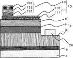
图1是采用本发明的正电极的发光器件的示意性截面图;1 is a schematic cross-sectional view of a light emitting device employing a positive electrode of the present invention;
图2是采用本发明的正电极且在实例中所制造的氮化镓基化合物半导体发光器件的示意性截面图;以及2 is a schematic cross-sectional view of a gallium nitride-based compound semiconductor light-emitting device manufactured in an example using the positive electrode of the present invention; and
图3是采用本发明的正电极且在实例中所制造的氮化镓基化合物半导体发光器件的示意性平面图。Fig. 3 is a schematic plan view of a gallium nitride-based compound semiconductor light emitting device manufactured in Example using the positive electrode of the present invention.
具体实施方式Detailed ways
图1是采用本发明正电极的发光器件的示意性截面图。参考标号10表示本发明的正电极,其由透明电极(11)和接合衬垫电极(13)构成。透明电极(11)例如由接触层(111)和电流扩散层(112)构成。接合衬垫电极(13)例如由反射层(131)、阻挡层(132)和最上层(133)构成;即,具有三层结构。参考标号1表示衬底,2表示GaN基化合物半导体层、其由n型半导体层(3)、发光层(4)和p型半导体层(5)构成,6表示缓冲层,以及20表示负电极。Fig. 1 is a schematic sectional view of a light emitting device employing a positive electrode of the present invention.
在具有透明正电极的面朝上型芯片中,从发光层(4)发射的光仅通过芯片的侧面以及通过没有被接合衬垫电极覆盖的透明电极提取出来。In a face-up chip with a transparent positive electrode, the light emitted from the light-emitting layer (4) is extracted only through the sides of the chip and through the transparent electrode not covered by the bonding pad electrode.
通过采用本发明的正电极,朝向接合衬垫电极(13)发射的光被用作接合衬垫电极的底部表面(即,与透明电极接触的表面)的反射层(131)反射。一些反射光线沿横向方向或倾斜方向被散射,而其它的光线被反射到接合衬垫电极下面的部分。沿横向方向或倾斜方向被散射的光线通过芯片的侧面被提取到外部,而被反射到接合衬垫电极下面的部分的光线通过芯片的底部表面被进一步散射或反射,并通过芯片的侧面以及通过透明电极的(没有被衬垫电极覆盖的)一部分提取出来。By employing the positive electrode of the present invention, light emitted toward the bonding pad electrode (13) is reflected by the reflective layer (131) serving as the bottom surface (ie, the surface in contact with the transparent electrode) of the bonding pad electrode. Some of the reflected light is scattered in lateral or oblique directions, while other light is reflected to the portion below the bonding pad electrode. The light scattered in the lateral direction or oblique direction is extracted to the outside through the side of the chip, and the light reflected to the part below the bonding pad electrode is further scattered or reflected through the bottom surface of the chip, and passes through the side of the chip and through the A portion of the transparent electrode (not covered by the pad electrode) is extracted.
用作接合衬垫电极的最底层的这样设置的反射层使在接合衬垫电极下面发射的光被提取到外部,从而获得高发射强度。比较而言,当接合衬垫电极的最底层吸收光时,在接合衬垫电极下面发射的光实际上被衬垫电极的最底层吸收,而没有被提取到外部。The reflective layer thus disposed serving as the bottommost layer of the bonding pad electrode allows light emitted under the bonding pad electrode to be extracted to the outside, thereby obtaining high emission intensity. In comparison, when the lowest layer of the bonding pad electrode absorbs light, light emitted under the bonding pad electrode is actually absorbed by the lowest layer of the bonding pad electrode without being extracted to the outside.
为了确实获得本发明的效果,必须使反射层直接接触透明电极。结果,必须使反射层牢固地附着到透明电极上,以使接合衬垫电极具有足够的强度。在常规的方法中,在将金丝连接到接合衬垫电极的步骤中,接合衬垫电极必须不从透明电极剥离。从而,优选作为剥离强度的反射层和透明电极的附着强度不小于490mN(50gf)。更优选不小于784mN(80gf)的剥离强度,最优选不小于980mN(100gf)的剥离强度。为了提高反射层和透明电极的附着强度,例如,存在这样的方法,其中在形成反射层之后预先处理透明电极的表面或者进行热处理。In order to surely obtain the effect of the present invention, it is necessary to directly contact the reflective layer with the transparent electrode. As a result, it is necessary to firmly attach the reflective layer to the transparent electrode so that the bonding pad electrode has sufficient strength. In the conventional method, in the step of connecting the gold wire to the bonding pad electrode, the bonding pad electrode must not be peeled off from the transparent electrode. Thus, it is preferable that the adhesion strength of the reflective layer and the transparent electrode as the peel strength is not less than 490 mN (50 gf). A peel strength of not less than 784 mN (80 gf) is more preferred, and a peel strength of not less than 980 mN (100 gf) is most preferred. In order to improve the adhesion strength of the reflective layer and the transparent electrode, for example, there is a method in which the surface of the transparent electrode is preliminarily treated or heat-treated after the reflective layer is formed.
根据形成反射层的材料而改变的反射层的反射率优选为60%或更高,更优选为80%或更高,进一步更优选为90%或更高。The reflectance of the reflective layer, which varies depending on the material forming the reflective layer, is preferably 60% or higher, more preferably 80% or higher, still more preferably 90% or higher.
利用例如分光光度计的设备可以容易地确定反射率。然而,很难确定接合衬垫电极的反射率,这是因为电极本身具有非常小的表面积。由此,在一种可选方法中,在形成接合衬垫电极期间,在反应室中提供例如由玻璃形成的宽的、透明的虚衬底。确定虚衬底上的接合衬垫电极的反射率。Reflectance can be readily determined using equipment such as a spectrophotometer. However, it is difficult to determine the reflectivity of bond pad electrodes because the electrodes themselves have very small surface areas. Thus, in an alternative method, during the formation of the bond pad electrodes, a wide, transparent dummy substrate, eg formed of glass, is provided in the reaction chamber. The reflectivity of the bond pad electrodes on the dummy substrate is determined.
接合衬垫电极的反射层优选由具有高反射率的金属形成。具体地,反射层优选由例如Pt、Rh、Ru或Ir的铂族金属;Al;Ag;或含有选自这些金属的至少一种金属元素的合金形成。在这些金属中,Al、Ag、Pt和含有选自这些金属的至少一种金属元素的合金通常用作电极材料,从而从可用性、易操作等的观点来看是优选的。The reflective layer to which the pad electrode is bonded is preferably formed of a metal having high reflectivity. Specifically, the reflective layer is preferably formed of a platinum group metal such as Pt, Rh, Ru, or Ir; Al; Ag; or an alloy containing at least one metal element selected from these metals. Among these metals, Al, Ag, Pt, and alloys containing at least one metal element selected from these metals are generally used as electrode materials, and thus are preferable from the viewpoints of usability, ease of handling, and the like.
在其中不形成开口或窗口的情况下,在透明电极上直接形成接合衬垫电极。当在透明电极上设置接合衬垫电极时,欧姆接触面积不减小,且即使在接合衬垫电极下面的部分中,电极的接触电阻也不增大。从而,可防止驱动电压的增加。另外,由于通过用作接合衬垫电极的最底部表面的反射层来反射已通过透明电极的光,可以抑制过多的光吸收。In the case where no opening or window is formed, the bonding pad electrode is directly formed on the transparent electrode. When the bonding pad electrode is provided on the transparent electrode, the ohmic contact area does not decrease, and the contact resistance of the electrode does not increase even in a portion below the bonding pad electrode. Thus, an increase in driving voltage can be prevented. In addition, since light that has passed through the transparent electrode is reflected by the reflective layer serving as the bottommost surface of the bonding pad electrode, excessive light absorption can be suppressed.
在透明电极上的任何位置处可以形成接合衬垫电极。例如,可以在离负电极最远的位置处或在芯片的中心处形成接合衬垫电极。然而,在过度靠近负电极的位置处形成的接合衬垫电极是不优选的,这是由于在接合期间,金属丝(wire)或球(ball)之间可能发生短路。The bonding pad electrode may be formed at any position on the transparent electrode. For example, the bonding pad electrode may be formed at the farthest position from the negative electrode or at the center of the chip. However, a bonding pad electrode formed at a position too close to the negative electrode is not preferable because a short circuit may occur between wires or balls during bonding.
接合衬垫电极优选具有尽可能大的表面积,以便于接合操作。然而,由于表面积变大,发射光的提取受到抑制。结果,芯片的输出显著下降。例如,当超过一半的芯片表面区域覆盖有衬垫电极时,发射光的提取受到抑制,导致输出显著下降,而当衬垫电极的表面积过小时,接合操作变得困难,导致产量降低。由此,优选衬垫电极的表面积稍大于接合球(bondingball)的直径。通常,衬垫电极具有其直径约为100μm的圆形的平面图。The bonding pad electrodes preferably have as large a surface area as possible to facilitate the bonding operation. However, the extraction of emitted light is inhibited due to the larger surface area. As a result, the chip's output dropped significantly. For example, when more than half of the chip surface area is covered with pad electrodes, the extraction of emitted light is suppressed, resulting in a significant drop in output, while when the surface area of the pad electrodes is too small, bonding operations become difficult, resulting in reduced yield. Therefore, it is preferable that the surface area of the pad electrode is slightly larger than the diameter of the bonding ball. Typically, the pad electrode has a circular plan view with a diameter of about 100 μm.
在接合衬垫电极的反射层由高反射率金属形成的情况下,反射层的厚度优选为20至3,000nm。当反射层过薄时,不能获得充分的反射,而当厚度过大时,形成反射层所需的周期延长了,并且材料成本增加;即,没有提供优点。更优选地,厚度为50至1,000nm,其中最优选100至500nm。In the case where the reflective layer bonding the pad electrode is formed of a high-reflectivity metal, the thickness of the reflective layer is preferably 20 to 3,000 nm. When the reflective layer is too thin, sufficient reflection cannot be obtained, and when the thickness is too large, the period required to form the reflective layer is prolonged, and the material cost increases; that is, no advantage is provided. More preferably, the thickness is from 50 to 1,000 nm, most preferably from 100 to 500 nm.
接合衬垫电极可以仅由上述高反射率金属形成。换句话说,接合衬垫电极可以仅由反射层构成。同时,各种材料和结构的接合衬垫电极已公知。从而,可以在任何公知的接合衬垫电极的半导体层侧(即,在透明电极侧)设置上述反射层。可选地,可以用上述反射层替代任何公知的接合衬垫电极的最底层(在半导体层侧)。The bonding pad electrode may be formed only of the above-mentioned high-reflectivity metal. In other words, the bonding pad electrode may consist of only the reflective layer. Meanwhile, bonding pad electrodes of various materials and structures are known. Thus, the above-mentioned reflective layer may be provided on the semiconductor layer side (ie, on the transparent electrode side) of any known bonding pad electrode. Alternatively, the above-mentioned reflective layer may be substituted for the bottommost layer (on the semiconductor layer side) of any known bonding pad electrode.
在接合衬垫电极的这种层叠结构的情况下,对反射层上的层叠部分没有特定的限制,可以采用任何结构的层叠部分。在层叠结构的接合衬垫电极中,在反射层上设置的层起着提高整个接合衬垫电极的强度的重要作用。从而,该层必须由具有相对高强度的金属材料形成或必须足够厚。从该观点来看,Ti、Cr和Al是理想的材料。在它们之中,从材料强度的观点来看优选Ti。在该层加强了接合衬垫电极的情况下,该层称为“阻挡层”。In the case of such a laminated structure of bonding pad electrodes, there is no specific limitation on the laminated portion on the reflective layer, and any structure of the laminated portion can be employed. In the bonding pad electrode having a laminated structure, the layer provided on the reflective layer plays an important role in increasing the strength of the bonding pad electrode as a whole. Thus, the layer must be formed of a metallic material having relatively high strength or must be sufficiently thick. From this point of view, Ti, Cr, and Al are ideal materials. Among them, Ti is preferable from the viewpoint of material strength. In the case where this layer reinforces the bonding pad electrode, this layer is referred to as a "barrier layer".
反射层也可以用作阻挡层。当反射层由具有高反射率和高强度的金属材料形成并且具有大厚度时,不需要形成额外的阻挡层。例如,当反射层由Al形成时,不需要阻挡层。Reflective layers can also be used as barrier layers. When the reflective layer is formed of a metal material having high reflectivity and strength and has a large thickness, it is not necessary to form an additional barrier layer. For example, when the reflective layer is formed of Al, the barrier layer is not required.
阻挡层优选具有20至3,000nm的厚度。当阻挡层过薄时,提高强度的效果是不够的,而当该层过厚时,没有获得特别的优点,仅仅发生成本的增加。更优选地,厚度为50至1,000nm,最优选为100至500nm。The barrier layer preferably has a thickness of 20 to 3,000 nm. When the barrier layer is too thin, the strength-enhancing effect is insufficient, and when the layer is too thick, no particular advantage is obtained and only an increase in cost occurs. More preferably, the thickness is 50 to 1,000 nm, most preferably 100 to 500 nm.
接合衬垫电极的最上层(在反射层的相反侧)优选由牢固地接合到接合球的材料形成。接合球通常由金构成,且Au和Al已公知具有对金接合球的优良的接合性能。在它们之中,特别优选金。最上层优选具有50至1,000nm的厚度,更优选100至500nm。当最上层过薄时,对接合球的接合性能是不够的,而当该层过厚时,没有获得特别的优点,仅仅是增加了成本。The uppermost layer of the bond pad electrode (on the opposite side from the reflective layer) is preferably formed of a material that bonds firmly to the bond ball. Bonding balls are generally composed of gold, and Au and Al are known to have excellent bonding properties to gold bonding balls. Among them, gold is particularly preferred. The uppermost layer preferably has a thickness of 50 to 1,000 nm, more preferably 100 to 500 nm. When the uppermost layer is too thin, the bonding performance to the bonding ball is insufficient, and when the layer is too thick, no particular advantage is obtained and only cost is increased.
在p型半导体层上形成的透明电极满足性能上的需要。优选的性能的实例包括与p型层的低接触电阻、优良的光学透射性(在发光器件是其中从发光器层发射的光通过电极侧被提取出来的面朝上安装型的情况下)、以及用于在整个p型层内均匀地扩散电流的优良的导电性。The transparent electrode formed on the p-type semiconductor layer satisfies performance requirements. Examples of preferable properties include low contact resistance with the p-type layer, excellent optical transmittance (in the case of the light emitting device being a face-up mounting type in which light emitted from the light emitter layer is extracted through the electrode side), and excellent electrical conductivity for spreading current uniformly throughout the p-type layer.
各种材料和结构的透明电极已经是公知的,在本发明中可以采用任何公知的透明电极而没有任何限制。然而,为了满足在性能上的上述需求,透明电极优选具有包含至少两层的结构;即,与p型层接触的接触层和设置在接触层上的并且促进电流扩散的电流扩散层。如果满足上述性能上的需求,当然,可以采用兼具接触层和电流扩散层的性能的一层。当采用一层结构时,优势是制造工艺的复杂性较小。Transparent electrodes of various materials and structures are known, and any known transparent electrodes may be employed in the present invention without any limitation. However, in order to meet the above-mentioned demands in performance, the transparent electrode preferably has a structure including at least two layers; namely, a contact layer in contact with the p-type layer and a current spreading layer provided on the contact layer and promoting current spreading. If the above performance requirements are satisfied, of course, a layer having both the performances of the contact layer and the current diffusion layer may be used. When using a one-layer structure, the advantage is that the manufacturing process is less complex.
要求接触层呈现对p型层的低接触电阻。从该观点来看,接触层优选由铂族金属如铂(Pt)、钌(Ru)、锇(Os)、铑(Rh)、铱(Ir)或钯(Pd)形成、或由其合金形成。在它们之中,Pt和Pt合金是特别优选的,这是由于相对于未经历高温热处理的具有相对高电阻的p型GaN基化合物半导体层,Pt和Pt合金在没有任何热处理的情况下具有高功函数并且可实现优良的欧姆接触。The contact layer is required to exhibit low contact resistance to the p-type layer. From this point of view, the contact layer is preferably formed of a platinum group metal such as platinum (Pt), ruthenium (Ru), osmium (Os), rhodium (Rh), iridium (Ir), or palladium (Pd), or an alloy thereof . Among them, Pt and Pt alloys are particularly preferable because Pt and Pt alloys have high work function and can achieve excellent ohmic contact.
在接触层由铂族金属或其合金形成的情况下,从光学透明度的观点来看,必须显著减小该层的厚度,优选为0.1至7.5nm。当厚度小于0.1nm时,不能可靠地形成这种薄膜,而当厚度超过7.5nm时,透明度降低。更优选地,厚度为5nm或更小。考虑到由于随后层叠电流扩散层以及所形成膜的稳定性所引起的透明度的降低,该厚度特别优选为0.5至2.5nm。In the case where the contact layer is formed of a platinum group metal or an alloy thereof, it is necessary to remarkably reduce the thickness of the layer, preferably 0.1 to 7.5 nm, from the viewpoint of optical transparency. When the thickness is less than 0.1 nm, such a thin film cannot be reliably formed, and when the thickness exceeds 7.5 nm, the transparency decreases. More preferably, the thickness is 5 nm or less. The thickness is particularly preferably 0.5 to 2.5 nm in consideration of a decrease in transparency due to the subsequent lamination of the current spreading layer and the stability of the formed film.
然而,当减小接触层的厚度时,接触层沿平面方向的电阻增加,由于p型层的比较高的电阻,电流扩散被限制到用作电流注入部分的接合衬垫电极的周围。结果,发射图形的均匀性降低,由此降低了发射输出。However, when the thickness of the contact layer is reduced, the resistance in the planar direction of the contact layer increases, and due to the relatively high resistance of the p-type layer, current diffusion is limited to the periphery of the bonding pad electrode serving as the current injection portion. As a result, the uniformity of the emission pattern decreases, thereby lowering the emission output.
当在接触层上设置具有高光透射率和高电导率的电流扩散层用作用于促进接触层的电流扩散性能的方法时,可以实现电流的均匀扩散,而不极大地削弱低接触电阻和铂族金属的光透射率,由此可以制造具有高输出的发光器件。When disposing a current spreading layer with high light transmittance and high electrical conductivity on the contact layer is used as a method for promoting the current spreading performance of the contact layer, uniform diffusion of current can be achieved without greatly impairing the low contact resistance and platinum group Light transmittance of metals, whereby light emitting devices with high output can be manufactured.
电流扩散层优选由具有高电导率的金属材料例如选自金、银和铜的金属;或含有这些金属中的至少一种的合金形成。在它们之中,金是最优选的,这是由于其薄膜呈现高光透射率。The current spreading layer is preferably formed of a metal material having high electrical conductivity such as a metal selected from gold, silver, and copper; or an alloy containing at least one of these metals. Among them, gold is most preferable since its thin film exhibits high light transmittance.
可选地,电流扩散层还可以由具有高电导率的透明材料如硫化锌和金属氧化物例如ITO、氧化锌、氧化锌铝、掺F的氧化锡、氧化钛、氧化铋和氧化镁形成。从高光透射率的观点来看,优选这种透明材料。在它们之中,已知ITO、氧化锌、氧化锌铝和掺F的氧化锡具有导电性,从而是最优选的。Alternatively, the current spreading layer may also be formed of a transparent material with high conductivity such as zinc sulfide and metal oxides such as ITO, zinc oxide, zinc aluminum oxide, F-doped tin oxide, titanium oxide, bismuth oxide, and magnesium oxide. Such a transparent material is preferable from the viewpoint of high light transmittance. Among them, ITO, zinc oxide, zinc aluminum oxide, and F-doped tin oxide are known to have conductivity and thus are most preferable.
在电流扩散层由金属形成的情况下,该层的厚度优选为1至20nm。当厚度小于1nm时,电流扩散效果差,而当厚度超过20nm时,电流扩散层的光学透明性显著下降,可能降低发射输出。更优选地,厚度为10nm或更小。此外,当厚度被控制为3至6nm时,电流扩散层具有均衡的光学透明性和电流扩散效果。通过结合这种电流扩散层和上述接触层,可以以高发射输出在正电极的整个表面上方获得均匀的发射。In the case where the current spreading layer is formed of metal, the thickness of the layer is preferably 1 to 20 nm. When the thickness is less than 1 nm, the current spreading effect is poor, and when the thickness exceeds 20 nm, the optical transparency of the current spreading layer is significantly lowered, possibly lowering the emission output. More preferably, the thickness is 10 nm or less. In addition, when the thickness is controlled to be 3 to 6 nm, the current spreading layer has balanced optical transparency and current spreading effect. By combining such a current spreading layer and the above-mentioned contact layer, uniform emission can be obtained over the entire surface of the positive electrode with high emission output.
在电流扩散层由透明材料形成的情况下,该层的厚度优选为10至5,000nm。当厚度小于10nm时,电流扩散效果差,而当厚度超过5,000nm时,电流扩散层的光学透明性显著下降,可能降低发射输出。更优选地,厚度为50至2,000nm。此外,当厚度被控制为100至1,000nm时,电流扩散层具有均衡的光学透明性和电流扩散效果。通过结合这种电流扩散层和上述接触层,可以以高输出在正电极的整个表面上方获得均匀的发射。In the case where the current spreading layer is formed of a transparent material, the thickness of the layer is preferably 10 to 5,000 nm. When the thickness is less than 10 nm, the current spreading effect is poor, and when the thickness exceeds 5,000 nm, the optical transparency of the current spreading layer is significantly lowered, possibly lowering the emission output. More preferably, the thickness is 50 to 2,000 nm. In addition, when the thickness is controlled to be 100 to 1,000 nm, the current spreading layer has balanced optical transparency and current spreading effect. By combining such a current spreading layer and the above-mentioned contact layer, uniform emission can be obtained with high output over the entire surface of the positive electrode.
在透明电极上形成接合衬垫电极的情况下,透明电极的最上层可以覆盖有金属或金属氧化物。In the case of forming the bonding pad electrode on the transparent electrode, the uppermost layer of the transparent electrode may be covered with metal or metal oxide.
透明电极的最上层可以是电流扩散层,并且电流扩散层可以覆盖有用于接合接合衬垫电极的层。由于用于接合的层的形成削弱了透明性,最上层优选为电流扩散层。The uppermost layer of the transparent electrode may be a current spreading layer, and the current spreading layer may be covered with a layer for bonding the bonding pad electrodes. Since the formation of a layer for bonding impairs transparency, the uppermost layer is preferably a current spreading layer.
可以在透明电极的最上表面上进行提取发射光的工序。在该工序中,例如,在透明电极的最上表面上设置凹入部分和/或凸出部分。可以通过利用构图或通过湿法处理来提供凹入部分和/或凸出部分。对凹入部分和/或凸出部分的形状没有特定限制,可以采用任何公知的形状如条形、网格和点。A process of extracting emitted light may be performed on the uppermost surface of the transparent electrode. In this process, for example, concave portions and/or convex portions are provided on the uppermost surface of the transparent electrode. The concave portion and/or the convex portion may be provided by using patterning or by wet processing. There is no particular limitation on the shape of the concave portion and/or the convex portion, and any known shape such as bars, grids, and dots may be employed.
并且,当在具有凹入部分和/或凸出部分的这种表面上形成接合衬垫电极时,可以提高反射层和透明电极的附着强度。Also, when the bonding pad electrode is formed on such a surface having the concave portion and/or the convex portion, the adhesion strength of the reflective layer and the transparent electrode can be improved.
对形成接触层、电流扩散层和接合衬垫电极的方法没有特定的限制,可以采用任何公知的方法例如真空气相淀积或溅射。There is no particular limitation on the method of forming the contact layer, current spreading layer and bonding pad electrode, and any known method such as vacuum vapor deposition or sputtering can be used.
本发明的正电极可应用于任何常规公知的半导体发光器件,包括氮化镓基化合物半导体发光器件,例如图1中所示的器件,其包括:衬底;通过缓冲层的媒介在衬底上层叠的氮化镓基化合物半导体层(即,n型半导体层、发光层和p型半导体层)。The positive electrode of the present invention can be applied to any conventionally known semiconductor light-emitting device, including a gallium nitride-based compound semiconductor light-emitting device, such as the device shown in Figure 1, which includes: a substrate; on the substrate through the medium of a buffer layer Laminated gallium nitride-based compound semiconductor layers (ie, n-type semiconductor layer, light-emitting layer, and p-type semiconductor layer).
对衬底的材料没有特定的限制,衬底可以由任何公知的材料形成。公知的材料的实例包括氧化物单晶如蓝宝石单晶(Al2O3;A平面、C平面、M平面或R平面)、尖晶石单晶(MgAl2O4)、ZnO单晶、LiAlO2单晶、LiGaO2单晶和MgO单晶;Si单晶;SiC单晶;GaAs单晶;AlN单晶;GaN单晶;以及硼化物单晶如ZrB2单晶。对衬底的晶向没有特定的限制。衬底的晶面可以对特定晶面倾斜或不倾斜。There is no particular limitation on the material of the substrate, and the substrate may be formed of any known material. Examples of known materials include oxide single crystals such as sapphire single crystals (Al2 O3 ; A plane, C plane, M plane, or R plane), spinel single crystals (MgAl2 O4 ), ZnO single crystals, LiAlO2 single crystal, LiGaO2 single crystal and MgO single crystal; Si single crystal; SiC single crystal; GaAs single crystal; AlN single crystal; GaN single crystal; and boride single crystal such as ZrB2 single crystal. There is no particular limitation on the crystal orientation of the substrate. The crystal planes of the substrate may or may not be tilted to a particular crystal plane.
对n型半导体层、发光层和p型半导体层的结构没有特定的限制,这些层可以具有各种已知的结构。P型半导体层可以具有常规的载流子浓度。值得注意的是,本发明的透明电极还可以应用于具有低载流子浓度(例如,大约1×1017cm-3)的p型半导体层。There is no particular limitation on the structures of the n-type semiconductor layer, light emitting layer, and p-type semiconductor layer, and these layers may have various known structures. The P-type semiconductor layer may have a conventional carrier concentration. It is worth noting that the transparent electrode of the present invention can also be applied to p-type semiconductor layers with low carrier concentration (for example, about 1×1017 cm−3 ).
在本发明中,对用于形成n型半导体层、发光层和p型半导体层的氮化镓基化合物半导体的类型没有特定的限制,可以采用由分子式AlxInyGa1-x-yN(0≤x<1,0≤y<1,0≤x+y<1)表示的常规公知的半导体。In the present invention, there is no specific limitation on the type of gallium nitride-based compound semiconductor used to form the n-type semiconductor layer, light-emitting layer and p-type semiconductor layer, and the formula Alx Iny Ga1-xy N(0 ≤x<1, 0≤y<1, 0≤x+y<1) represents a conventionally known semiconductor.
对用于生长这些氮化镓半导体的方法没有特定的限制,可以采用任何公知的方法来生长III族氮化物半导体、例如MOCVD(金属有机化学气相淀积)、HVPE(氢化物气相外延)或MBE(分子束外延)。从层厚度可控性和批量生产率的观点来看,优选采用MOCVD。在MOCVD的情况下,采用氢气(H2)或氮气(N2)作为载气,采用三甲基镓(TMG)或三乙基镓(TEG)作为Ga(III族元素)源,采用三甲基铝(TMA)或三乙基铝(TEA)作为Al(III族元素)源,采用三甲基铟(TMI)或三乙基铟(TEI)作为In(III族元素)源,以及采用氨(NH3)、肼(N2H4)等作为N(V族元素)源。另外,采用用作Si源的甲硅烷(SiH4)或乙硅烷(Si2H6)、或者用作Ge源的锗烷(GeH4)或有机锗化合物作为n型掺杂剂,而采用用作Mg源的双(环戊二烯基)镁(Cp2Mg)或双(乙基环戊二烯基)镁((EtCp)2Mg)作为p型掺杂剂。There is no particular limitation on the method for growing these gallium nitride semiconductors, and any known method may be used for growing Group III nitride semiconductors, such as MOCVD (Metal Organic Chemical Vapor Deposition), HVPE (Hydride Vapor Phase Epitaxy), or MBE (Molecular Beam Epitaxy). From the viewpoint of layer thickness controllability and mass productivity, MOCVD is preferably employed. In the case of MOCVD, hydrogen (H2 ) or nitrogen (N2 ) is used as the carrier gas, trimethylgallium (TMG) or triethylgallium (TEG) is used as the Ga (group III element) source, trimethylgallium (TMG) aluminum (TMA) or triethylaluminum (TEA) as the source of Al (Group III elements), trimethylindium (TMI) or triethylindium (TEI) as the source of In (Group III elements), and ammonia (NH3 ), hydrazine (N2 H4 ) and the like are used as N (group V element) sources. In addition, monosilane (SiH4 ) or disilane (Si2 H6 ) used as a source of Si, or germane (GeH4 ) or an organic germanium compound used as a source of Ge is used as an n-type dopant, while Bis(cyclopentadienyl)magnesium (Cp2 Mg) or bis(ethylcyclopentadienyl)magnesium ((EtCp)2 Mg) as a Mg source was used as a p-type dopant.
为了使负电极附着到包括衬底以及连续设置在衬底的顶部上的n型半导体层、发光层和p型半导体层的氮化镓基化合物半导体结构,以使负电极与n型半导体层接触,去除一部分发光层和一部分p型半导体层,以便露出n型半导体层。此后,在剩余的p型半导体层上形成本发明的正电极,并在露出的n型半导体层上形成负电极。对负电极的组成和结构没有特定的限制,可以采用任何公知的负电极。In order to attach the negative electrode to the gallium nitride-based compound semiconductor structure including the substrate and the n-type semiconductor layer, the light-emitting layer, and the p-type semiconductor layer continuously disposed on top of the substrate, such that the negative electrode is in contact with the n-type semiconductor layer , removing a part of the light emitting layer and a part of the p-type semiconductor layer, so as to expose the n-type semiconductor layer. Thereafter, the positive electrode of the present invention is formed on the remaining p-type semiconductor layer, and the negative electrode is formed on the exposed n-type semiconductor layer. There are no specific limitations on the composition and structure of the negative electrode, and any known negative electrode can be used.
当采用对具有落入在发射波长范围内的波长的光透明的衬底如蓝宝石和SiC时,可以在衬底的背面上设置反射膜。当设置反射膜时,可以减少在衬底的底部处的发射光的损耗。从而,可以进一步提高对发射光的提取效率。When using a substrate transparent to light having a wavelength falling within the emission wavelength range such as sapphire and SiC, a reflective film may be provided on the back surface of the substrate. When the reflective film is provided, loss of emitted light at the bottom of the substrate can be reduced. Thus, the extraction efficiency of emitted light can be further improved.
并且,可以进行这样的工序,通过其在半导体或透明电极的表面上、或衬底的背面上设置凹入部分和/或凸出部分。结果,可进一步提高对发射光的提取效率。通过该工序可以形成相对于衬底倾斜的表面以及垂直表面。为了防止多次反射,优选形成倾斜表面。可以通过研磨半导体或透明电极的表面或衬底的背面来进行该工序。可选地,可以通过采用透明材料的结构来进行该工序。Also, a process may be performed by which concave portions and/or convex portions are provided on the surface of the semiconductor or the transparent electrode, or on the back surface of the substrate. As a result, the extraction efficiency of emitted light can be further improved. Through this process, a surface inclined with respect to the substrate and a vertical surface can be formed. In order to prevent multiple reflections, it is preferable to form an inclined surface. This process can be performed by grinding the surface of the semiconductor or transparent electrode or the back surface of the substrate. Alternatively, this process can be performed by employing a structure of a transparent material.
通过将本发明的正电极用于半导体发光器件,可以制造呈现高发射强度的氮化镓基化合物半导体发光器件。换句话说,基于该技术可以制造高亮度LED。从而,可以在低电功率下驱动均采用了基于该技术制造的芯片的电子设备如移动式电话和显示面板;均采用了任何该电子设备的机器和装置如汽车、计算机和游戏机,并实现了优良的特性。特别地,在由电池驱动的移动式电话、游戏机、玩具和汽车部件中显著地获得了电功率节省效果。By using the positive electrode of the present invention for a semiconductor light emitting device, a gallium nitride-based compound semiconductor light emitting device exhibiting high emission intensity can be manufactured. In other words, high-brightness LEDs can be manufactured based on this technology. Thereby, electronic equipment such as mobile phones and display panels each employing chips manufactured based on this technology can be driven at low electric power; machines and devices such as automobiles, computers, and game machines each employing any of this electronic equipment, and realize Excellent properties. In particular, electric power saving effects are remarkably obtained in battery-driven mobile phones, game machines, toys, and automobile parts.
实例example
下面将通过实例将更详细地介绍本发明,其不应被解释为将本发明限制于此。The present invention will be described in more detail below by way of examples, which should not be construed as limiting the present invention thereto.
<实例1><Example 1>
图2示出了在该实例中制造的氮化镓基化合物半导体发光器件的截面图,以及图3示出了其平面图。通过下列工序制造氮化镓化合物半导体层叠结构。在蓝宝石衬底(1)上形成AlN缓冲层(6),并在缓冲层上,依序形成下列层:未掺杂的GaN底衬层(undercoat layer)(厚度:8μm)(3a);Si掺杂的n型GaN接触层(厚度:2μm)(3b);n型In0.1Ga0.9N覆层(厚度:250nm)(3c);包括Si掺杂的GaN势垒层(5层和一个最终层,每层厚度:16nm)和In0.2Ga0.8N阱层(5层,每层厚度:2.5nm)的多量子阱结构的发光层(4);Mg掺杂的p型Al0.07Ga0.93N覆层(厚度:0.01μm)(5a);以及Mg掺杂的p型GaN接触层(厚度:0.15μm)(5b)。在氮化镓基化合物半导体层叠结构的p型GaN接触层上,形成本发明的正电极(10),正电极由下列层构成:包括Pt接触层(厚度:1.5nm)(111)和Au电流扩散层(厚度:5nm)(112)的透明电极(11);以及具有由Pt层(厚度:50nm)(13a)、Ti层(厚度:20nm)(13b)、Al层(厚度:10nm)(13c)、Ti层(厚度:100nm)(13d)和Au层(厚度:200nm)(13e)构成的五层结构的接合衬垫电极(13)。在形成接合衬垫电极的五层之中,具有高反射率的Pt层(厚度:50nm)(13a)用作反射层。在n型GaN接触层上,形成具有Ti/Au双层结构的负电极(20)。由此制造的发光器件的半导体侧用作光提取侧。图3示出了正电极和负电极的结构。FIG. 2 shows a cross-sectional view of a gallium nitride-based compound semiconductor light-emitting device manufactured in this example, and FIG. 3 shows a plan view thereof. The gallium nitride compound semiconductor laminated structure was produced through the following procedures. An AlN buffer layer (6) was formed on a sapphire substrate (1), and on the buffer layer, the following layers were sequentially formed: an undoped GaN undercoat layer (thickness: 8 μm) (3a); Si Doped n-type GaN contact layer (thickness: 2 μm) (3b); n-type In0.1 Ga0.9 N cladding layer (thickness: 250 nm) (3c); including Si-doped GaN barrier layer (5 layers and a final layers, each layer thickness: 16nm) and In0.2 Ga0.8 N well layers (5 layers, each layer thickness: 2.5nm) light-emitting layer (4) of the multi-quantum well structure; Mg-doped p-type Al0.07 Ga0.93 N A cladding layer (thickness: 0.01 μm) (5a); and a Mg-doped p-type GaN contact layer (thickness: 0.15 μm) (5b). On the p-type GaN contact layer of the GaN-based compound semiconductor laminated structure, the positive electrode (10) of the present invention is formed, and the positive electrode is composed of the following layers: including the Pt contact layer (thickness: 1.5nm) (111) and the Au current A transparent electrode (11) of a diffusion layer (thickness: 5nm) (112); 13c), a Ti layer (thickness: 100nm) (13d) and an Au layer (thickness: 200nm) (13e) to form a five-layer bonding pad electrode (13). Among the five layers forming the bonding pad electrode, a Pt layer (thickness: 50 nm) (13a) having a high reflectance was used as a reflective layer. On the n-type GaN contact layer, a negative electrode (20) having a Ti/Au double layer structure is formed. The semiconductor side of the light emitting device thus manufactured serves as the light extraction side. Fig. 3 shows the structure of positive and negative electrodes.
在上述层叠结构中,n型GaN接触层具有1×1019cm-3的载流子浓度,GaN势垒层具有1×1018cm-3的Si掺杂剂浓度,p型GaN接触层具有5×1018cm-3的载流子浓度,以及p型AlGaN覆层具有5×1019cm-3的Mg掺杂剂浓度。In the above stacked structure, the n-type GaN contact layer has a carrier concentration of 1×1019 cm-3 , the GaN barrier layer has a Si dopant concentration of 1×1018 cm-3 , and the p-type GaN contact layer has The carrier concentration of 5×1018 cm−3 , and the p-type AlGaN cladding layer has a Mg dopant concentration of 5×1019 cm−3 .
在众所周知的典型条件下通过MOCVD层叠这些氮化镓化合物半导体层。通过下列工序形成正电极和负电极。These gallium nitride compound semiconductor layers are stacked by MOCVD under well-known typical conditions. The positive and negative electrodes were formed through the following procedures.
通过下列工序利用反应离子蚀刻来露出将要在其上设置负电极的一部分n型GaN接触层。A portion of the n-type GaN contact layer on which the negative electrode is to be provided is exposed using reactive ion etching through the following procedure.
首先,通过下列工序在p型半导体层上形成蚀刻掩模。将光致抗蚀剂施加在半导体层叠结构的整个表面上,通过公知的光刻技术除去一部分抗蚀剂,该部分比正电极稍大。将由此处理过的层叠结构置于真空气相淀积装置中,并在4×10⁻⁴Pa或更低的压力下通过电子束方法层叠Ni(厚度:约50nm)和Ti(厚度:约300nm)。随后,通过剥离(lift-off)从正电极区域以外的区域去除层叠的金属膜以及光致抗蚀剂。First, an etching mask was formed on the p-type semiconductor layer through the following procedures. A photoresist is applied over the entire surface of the semiconductor stacked structure, and a portion of the resist, which is slightly larger than the positive electrode, is removed by known photolithography. The laminated structure thus processed was placed in a vacuum vapor deposition apparatus, and Ni (thickness: about 50 nm) and Ti (thickness: about 300 nm) were laminated by an electron beam method at a pressure of 4×10⁻⁴ Pa or less . Subsequently, the laminated metal film and the photoresist are removed from regions other than the positive electrode region by lift-off.
在反应离子蚀刻装置的蚀刻反应室中设置的一个电极上,放置半导体层叠结构。将蚀刻反应室抽真空到10-4Pa,并将蚀刻气体(Cl2)供给至已被抽真空的反应室内。进行蚀刻,直到露出n型GaN接触层。在完成蚀刻之后,从反应离子蚀刻装置中移走该结构,并用硝酸和氢氟酸去除蚀刻掩模。On one electrode provided in an etching reaction chamber of a reactive ion etching apparatus, a semiconductor stacked structure is placed. The etching reaction chamber was evacuated to 10-4 Pa, and an etching gas (Cl2 ) was supplied into the evacuated reaction chamber. Etching is performed until the n-type GaN contact layer is exposed. After the etching was completed, the structure was removed from the reactive ion etching apparatus, and the etching mask was removed with nitric acid and hydrofluoric acid.
随后,通过公知的光刻和剥离技术,仅在用于形成正电极的区域中在p型GaN接触层上形成由Pt构成的接触层和由Au构成的电流扩散层。在形成接触层和电流扩散层时,将氮化镓基化合物半导体层的层叠结构置于真空气相淀积装置中,并在p型GaN接触层上依序层叠Pt(1.5nm)和Au(5nm)。在从真空反应室中移开层叠结构之后,用广泛公知的剥离工序处理层叠结构。以类似的方式,在电流扩散层的一部分上,依序形成Pt反射层(13a)、Ti阻挡层(13b)、Al阻挡层(13c)、Ti阻挡层(13d)和Au最上层(13e),以由此形成接合衬垫电极(13)。从而,在p型GaN接触层上形成本发明的正电极。Subsequently, a contact layer composed of Pt and a current diffusion layer composed of Au were formed on the p-type GaN contact layer only in the region for forming the positive electrode by known photolithography and lift-off techniques. When forming the contact layer and the current diffusion layer, the stacked structure of gallium nitride-based compound semiconductor layers is placed in a vacuum vapor deposition device, and Pt (1.5nm) and Au (5nm) are sequentially stacked on the p-type GaN contact layer. ). After removing the stacked structure from the vacuum reaction chamber, the stacked structure is processed by a widely known lift-off procedure. In a similar manner, on a part of the current spreading layer, a Pt reflective layer (13a), a Ti barrier layer (13b), an Al barrier layer (13c), a Ti barrier layer (13d) and an Au uppermost layer (13e) are sequentially formed , to thereby form a bonding pad electrode (13). Thus, the positive electrode of the present invention is formed on the p-type GaN contact layer.
在由此露出的n型GaN接触层上,通过下列工序形成负电极。首先,将抗蚀剂施加到结构的整个表面上,并通过公知的光刻技术去除在露出的n型GaN接触层上用于形成负电极的一部分抗蚀剂。通过常规采用的真空气相淀积,在半导体层上依序淀积Ti(100nm)和Au(200nm),以由此形成负电极。此后,通过常规的方法去除抗蚀剂。On the n-type GaN contact layer thus exposed, a negative electrode was formed through the following procedure. First, a resist is applied to the entire surface of the structure, and a part of the resist for forming a negative electrode on the exposed n-type GaN contact layer is removed by a well-known photolithography technique. Ti (100 nm) and Au (200 nm) were sequentially deposited on the semiconductor layer by conventionally employed vacuum vapor deposition, to thereby form a negative electrode. Thereafter, the resist is removed by a conventional method.
研磨和抛光具有正电极和负电极的由此形成的晶片的衬底的背面,以由此将衬底厚度调整到80μm,接着通过利用激光划片器在半导体层叠的层侧刻划晶片并通过芯片分割线切割,以由此制造正方形芯片(350μm×350μm)。通过利用探针的测量,发现在20mA的施加电流下各个芯片的正向电压为2.9V。The backside of the substrate of the thus formed wafer having positive and negative electrodes was ground and polished to thereby adjust the substrate thickness to 80 μm, followed by scribing the wafer on the layer side of the semiconductor stack by using a laser scriber and passing Die-separating wire dicing to thereby manufacture square chips (350 μm×350 μm). By measurement with a probe, it was found that the forward voltage of each chip was 2.9 V at an applied current of 20 mA.
在TO-18封装管壳内安装芯片。通过利用测试器的测量,发现在20mA的施加电流下芯片的发射输出为4.5mW。来自发光表面的发射的分布表明,光发射出现在与表面上方的正电极对应的发光表面的整个区域内。Install the chip in the TO-18 package. By measurement with a tester, it was found that the emission output of the chip was 4.5 mW at an applied current of 20 mA. The distribution of the emission from the light-emitting surface shows that light emission occurs over the entire area of the light-emitting surface corresponding to the positive electrode above the surface.
发现在实例1中制造的反射层在470nm的波长区域中具有92%的反射率。借助于分光光度计利用由玻璃制成的虚衬底来确定反射率,在形成接合衬垫电极期间玻璃制成的虚衬底已被置于同一反应室内。The reflective layer produced in Example 1 was found to have a reflectance of 92% in the wavelength region of 470 nm. The reflectance was determined by means of a spectrophotometer using a dummy substrate made of glass which had been placed in the same reaction chamber during the formation of the bonding pad electrodes.
并且,通过常规的剪力测试器(shear tester)来确定接合衬垫电极的剥离强度。发现剥离强度平均不小于980mN(100gf),没有什么可从透明电极脱落的。And, the peel strength of the bonding pad electrode was determined by a conventional shear tester. It was found that the peel strength was not less than 980 mN (100 gf) on average, and there was nothing to peel off from the transparent electrode.
<比较实例1><Comparative example 1>
除了在形成了接合衬垫电极的区域中没有设置透明电极、以及接合衬垫电极不具有反射层(13a)以外,重复例1的工序,以由此制造发光器件。从而,在比较例1中,接合衬垫电极的最底层(在半导体侧)是Ti层(13b),其与p型接触层(5b)直接接触。The procedure of Example 1 was repeated except that no transparent electrode was provided in the region where the bonding pad electrode was formed, and the bonding pad electrode did not have the reflective layer (13a), to thereby manufacture a light emitting device. Thus, in Comparative Example 1, the lowest layer (on the semiconductor side) of the bonding pad electrode is the Ti layer (13b), which is in direct contact with the p-type contact layer (5b).
为了建立电接触,使接合衬垫电极的周围与透明电极接触,其中接触面积约为接合衬垫电极的面积的5%。电流通过接触部分从接合衬垫电极流向透明电极。To establish electrical contact, the periphery of the bond pad electrode is brought into contact with the transparent electrode, wherein the contact area is about 5% of the area of the bond pad electrode. Electric current flows from the bonding pad electrode to the transparent electrode through the contact portion.
以与实例1的方式相同的方式来评估由此制造的发光器件,发现正向电压和发射输出分别为3.1V和4.2mW。来自发光表面的发射的分布表明,在对应于区域上方的接合衬垫电极的区域中没有发生光发射。这些结果表面,与Pt相比,Ti具有相对于p型接触层(5b)更高的接触电阻和更低的反射率。The light-emitting device thus manufactured was evaluated in the same manner as in Example 1, and the forward voltage and emission output were found to be 3.1 V and 4.2 mW, respectively. The distribution of emission from the light emitting surface shows that no light emission occurs in the region corresponding to the bond pad electrode above the region. These results suggest that Ti has higher contact resistance and lower reflectivity with respect to the p-type contact layer (5b) than Pt.
<实例2><Example 2>
除了将透明电极(11)的Pt接触层(111)的厚度调整为1nm;除了采用通过溅射形成的具有100nm厚度的ITO膜作为电流扩散层(112);以及除了由Al形成接合衬垫电极的反射层(13a)以外,重复实例1的工序,以由此制造发光器件。Except that the thickness of the Pt contact layer (111) of the transparent electrode (11) is adjusted to 1 nm; except that an ITO film having a thickness of 100 nm formed by sputtering is used as the current diffusion layer (112); and except that the bonding pad electrode is formed of Al Except for the reflective layer (13a) of , the procedure of Example 1 was repeated to thereby fabricate a light-emitting device.
以与实例1的方式相同的方式来评估由此制造的发光器件,发现正向电压和发射输出分别为2.9V和5.0mW。The light-emitting device thus manufactured was evaluated in the same manner as in Example 1, and the forward voltage and emission output were found to be 2.9 V and 5.0 mW, respectively.
并且,通过常规的剪力测试器来确定接合衬垫电极的剥离强度。在多个样品中发现剥离强度平均不小于980mN(100gf),但在接合衬垫电极和透明电极之间的界面处发生脱落。And, the peel strength of the bonding pad electrode was determined by a conventional shear tester. The peel strength was found to be not less than 980 mN (100 gf) on average in a plurality of samples, but peeling occurred at the interface between the bonding pad electrode and the transparent electrode.
<比较实例2><Comparative example 2>
除了接合衬垫电极(13)不具有反射层(13a)以外,重复实例1的工序,由此制造发光器件。以与实例1的方式相同的方式来评估由此制造的发光器件。结果,发现正向电压为2.9V,这与实例2的低值相同,但发射输出降低到4.7mW。The procedure of Example 1 was repeated except that the bonding pad electrode (13) did not have the reflective layer (13a), thereby manufacturing a light emitting device. The light-emitting device thus manufactured was evaluated in the same manner as in Example 1. As a result, the forward voltage was found to be 2.9 V, which was the same as the low value of Example 2, but the emission output was lowered to 4.7 mW.
<实例3><Example 3>
在该实例中,以与例1相似的方式通过下列工序来制造氮化镓化合物半导体层叠结构。在蓝宝石衬底(1)上形成AlN缓冲层(6),并在缓冲层上,依序形成下列层:未掺杂的GaN底衬层(厚度:6μm)(3a);Ge掺杂的n型GaN接触层(厚度:4μm)(3b);Si掺杂的n型In0.1Ga0.9N覆层(厚度:180nm)(3c);包括Si掺杂的GaN势垒层(5层和一个最终层,每层厚度:16nm)和In0.2Ga0.8N阱层(5层,每层厚度:2.5nm)的多量子阱结构的发光层(4);Mg掺杂的p型Al0.07Ga0.93N覆层(厚度:0.01μm)(5a);Mg掺杂的p型Al0.02Ga0.98N接触层(厚度:0.175μm)(5b);以及Ge掺杂的n型GaN隧穿层(厚度:20nm)(未示出)。在氮化镓基化合物半导体层叠结构的Ge掺杂的n型GaN隧穿层上,形成本发明的正电极(10),正电极由下列层构成:仅由ITO电流扩散层(厚度:250nm)(112)构成的透明电极(11);以及具有由Al层(厚度:50nm)(13a)、Ti层(厚度:20nm)(13b)、Al层(厚度:10nm)(13c)、Ti层(厚度:100nm)(13d)和Au层(厚度:200nm)(13e)构成的五层结构的接合衬垫电极(13)。在形成接合衬垫电极的五层之中,具有高反射率的Al层(厚度:50nm)(13a)用作反射层。在n型GaN接触层上,形成具有Ti/Au双层结构的负电极(20)。由此制造的发光器件的半导体侧用作光提取侧。图3示出了正电极和负电极的结构。In this example, a gallium nitride compound semiconductor laminated structure was produced in a similar manner to Example 1 through the following procedures. An AlN buffer layer (6) is formed on a sapphire substrate (1), and on the buffer layer, the following layers are sequentially formed: an undoped GaN underlayer (thickness: 6 μm) (3a); Ge-doped n Type GaN contact layer (thickness: 4μm) (3b); Si-doped n-type In0.1 Ga0.9 N cladding layer (thickness: 180nm) (3c); including Si-doped GaN barrier layer (5 layers and a final Layer, each layer thickness: 16nm) and In0.2 Ga0.8 N well layer (5 layers, each layer thickness: 2.5nm) light emitting layer (4) of the multi-quantum well structure; Mg-doped p-type Al0.07 Ga0.93 N cladding layer (thickness: 0.01 μm) (5a); Mg-doped p-type Al0.02 Ga0.98 N contact layer (thickness: 0.175 μm) (5b); and Ge-doped n-type GaN tunneling layer (thickness: 20nm ) (not shown). On the Ge-doped n-type GaN tunneling layer of the GaN-based compound semiconductor laminated structure, form the positive electrode (10) of the present invention, the positive electrode is made of the following layers: only by the ITO current diffusion layer (thickness: 250nm) (112) the transparent electrode (11) that constitutes; And have by Al layer (thickness: 50nm) (13a), Ti layer (thickness: 20nm) (13b), Al layer (thickness: 10nm) (13c), Ti layer ( A five-layer bonding pad electrode (13) composed of a thickness: 100 nm) (13d) and an Au layer (thickness: 200 nm) (13e). Among the five layers forming the bonding pad electrode, an Al layer (thickness: 50 nm) (13a) having a high reflectance was used as a reflective layer. On the n-type GaN contact layer, a negative electrode (20) having a Ti/Au double layer structure is formed. The semiconductor side of the light emitting device thus manufactured serves as the light extraction side. Fig. 3 shows the structure of positive and negative electrodes.
在上述层叠结构中,n型GaN接触层具有8×1018cm-3的载流子浓度,n型InGaN覆层具有7×1018cm-3的Si掺杂剂浓度,GaN势垒层具有1×1017cm-3的Si掺杂剂浓度,p型AlGaN接触层具有5×1017cm-3的载流子浓度,p型AlGaN覆层具有2×1020cm-3的Mg掺杂剂浓度,以及n型GaN隧穿层具有2×1019cm-3的Ge掺杂剂浓度。In the above stacked structure, the n-type GaN contact layer has a carrier concentration of 8×1018 cm-3 , the n-type InGaN cladding layer has a Si dopant concentration of 7×1018 cm-3 , and the GaN barrier layer has Si dopant concentration of 1×1017 cm-3 , the p-type AlGaN contact layer has a carrier concentration of 5×1017 cm-3 , and the p-type AlGaN cladding layer has a Mg doping of 2×1020 cm-3 dopant concentration, and the n-type GaN tunneling layer has a Ge dopant concentration of 2×1019 cm−3 .
以与实例1的方式相同的方式来评估由此制造的发光器件,发现正向电压和发射输出分别为3.2V和8.5mW。The light-emitting device thus produced was evaluated in the same manner as in Example 1, and the forward voltage and emission output were found to be 3.2 V and 8.5 mW, respectively.
并且,通过常规的剪力测试器来确定接合衬垫电极的剥离强度。在多个样品中发现剥离强度平均不小于980mN(100gf),但在接合衬垫电极和透明电极之间的界面处发生脱落。And, the peel strength of the bonding pad electrode was determined by a conventional shear tester. The peel strength was found to be not less than 980 mN (100 gf) on average in a plurality of samples, but peeling occurred at the interface between the bonding pad electrode and the transparent electrode.
工业适用性Industrial applicability
采用本发明正电极的半导体发光器件呈现低驱动电压和高发射强度。从而,该发光器件可显著有效地用于制造灯或类似的装置。The semiconductor light emitting device using the positive electrode of the present invention exhibits low driving voltage and high emission intensity. Thus, the light emitting device can be used remarkably effectively to manufacture lamps or the like.
Claims (27)
Applications Claiming Priority (3)
| Application Number | Priority Date | Filing Date | Title |
|---|---|---|---|
| JP222336/2004 | 2004-07-29 | ||
| JP2004222336 | 2004-07-29 | ||
| US60/599,571 | 2004-08-09 |
Publications (2)
| Publication Number | Publication Date |
|---|---|
| CN1993837A CN1993837A (en) | 2007-07-04 |
| CN100590898Ctrue CN100590898C (en) | 2010-02-17 |
Family
ID=38176830
Family Applications (1)
| Application Number | Title | Priority Date | Filing Date |
|---|---|---|---|
| CN200580025689AExpired - LifetimeCN100590898C (en) | 2004-07-29 | 2005-07-28 | Positive electrode for semiconductor light emitting devices |
Country Status (4)
| Country | Link |
|---|---|
| JP (4) | JP2009033210A (en) |
| KR (1) | KR100895452B1 (en) |
| CN (1) | CN100590898C (en) |
| TW (1) | TWI275190B (en) |
Cited By (1)
| Publication number | Priority date | Publication date | Assignee | Title |
|---|---|---|---|---|
| US20210252638A1 (en)* | 2020-02-17 | 2021-08-19 | Samsung Sdi Co., Ltd. | Laser welding method and monitoring method for secondary battery |
Families Citing this family (27)
| Publication number | Priority date | Publication date | Assignee | Title |
|---|---|---|---|---|
| KR101113878B1 (en)* | 2006-06-23 | 2012-03-09 | 엘지이노텍 주식회사 | Light emitting diode having vertical topology and method of making the same |
| JP2008177525A (en) | 2006-12-20 | 2008-07-31 | Showa Denko Kk | Group III nitride semiconductor light emitting device manufacturing method, group III nitride semiconductor light emitting device, and lamp |
| WO2009113659A1 (en)* | 2008-03-13 | 2009-09-17 | 昭和電工株式会社 | Semiconductor light-emitting device and method for manufacturing the same |
| KR100986518B1 (en)* | 2008-06-16 | 2010-10-07 | 엘지이노텍 주식회사 | Semiconductor light emitting device |
| CN102124574B (en)* | 2008-06-16 | 2013-07-17 | 丰田合成株式会社 | Semiconductor light emitting element, electrode and manufacturing method for the element, and lamp |
| USPP22761P2 (en) | 2010-04-23 | 2012-05-29 | Spring Meadow Nursery, Inc. | Potentilla plant named ‘White Lady’ |
| US8716723B2 (en) | 2008-08-18 | 2014-05-06 | Tsmc Solid State Lighting Ltd. | Reflective layer between light-emitting diodes |
| US9293656B2 (en)* | 2012-11-02 | 2016-03-22 | Epistar Corporation | Light emitting device |
| WO2010071113A1 (en) | 2008-12-15 | 2010-06-24 | 昭和電工株式会社 | Semiconductor light emission element |
| JP5350833B2 (en)* | 2009-02-20 | 2013-11-27 | 株式会社東芝 | Semiconductor light emitting device, semiconductor light emitting device, and method for manufacturing semiconductor light emitting device |
| WO2010113399A1 (en) | 2009-04-02 | 2010-10-07 | パナソニック株式会社 | Nitride semiconductor element and method for producing the same |
| CN101859838B (en)* | 2009-04-07 | 2014-09-10 | 裕星企业有限公司 | Light-emitting diode structure |
| KR101081166B1 (en)* | 2009-09-23 | 2011-11-07 | 엘지이노텍 주식회사 | Light emitting device, method for fabricating the same and light emitting device package |
| KR101103892B1 (en)* | 2009-12-08 | 2012-01-12 | 엘지이노텍 주식회사 | Light emitting device and light emitting device package |
| EP2555257A1 (en)* | 2010-04-01 | 2013-02-06 | Panasonic Corporation | Nitride semiconductor element and manufacturing method therefor |
| CN101846256A (en)* | 2010-05-04 | 2010-09-29 | 蔡州 | LED light source |
| CN102810613B (en)* | 2011-05-30 | 2016-04-13 | 比亚迪股份有限公司 | Current spread electrode, light emitting semiconductor device and preparation method thereof |
| JP6077201B2 (en) | 2011-08-11 | 2017-02-08 | 昭和電工株式会社 | Light emitting diode and manufacturing method thereof |
| JP5639626B2 (en) | 2012-01-13 | 2014-12-10 | シャープ株式会社 | Semiconductor light emitting device and electrode film forming method |
| JP5888132B2 (en)* | 2012-06-08 | 2016-03-16 | 豊田合成株式会社 | Method for manufacturing light emitting device |
| TWI514628B (en)* | 2013-10-24 | 2015-12-21 | Lextar Electronics Corp | Electrode structure and light emitting diode structure with electrode structure |
| KR101561198B1 (en)* | 2013-11-12 | 2015-10-19 | 주식회사 세미콘라이트 | Semiconductor light emitting device |
| KR101628244B1 (en)* | 2014-02-11 | 2016-06-21 | 주식회사 세미콘라이트 | Semiconductor light emitting device |
| CN104409601A (en)* | 2014-11-05 | 2015-03-11 | 扬州中科半导体照明有限公司 | Flip light-emitting diode chip with double reflection layers |
| CN107123594B (en)* | 2017-05-10 | 2019-11-26 | 湘能华磊光电股份有限公司 | LED electrode production method, LED electrode and LED chip |
| CN112289900B (en)* | 2020-09-16 | 2021-10-08 | 华灿光电(苏州)有限公司 | Ultraviolet light emitting diode epitaxial wafer and preparation method thereof |
| CN116364827B (en)* | 2023-05-29 | 2023-08-29 | 江西兆驰半导体有限公司 | Mini LED and preparation method thereof |
Family Cites Families (18)
| Publication number | Priority date | Publication date | Assignee | Title |
|---|---|---|---|---|
| JP2566207Y2 (en)* | 1992-10-21 | 1998-03-25 | 日亜化学工業株式会社 | Gallium nitride based light emitting device with current injection |
| JP3717196B2 (en)* | 1994-07-19 | 2005-11-16 | 豊田合成株式会社 | Light emitting element |
| JP3468644B2 (en)* | 1996-10-22 | 2003-11-17 | 豊田合成株式会社 | Group III nitride semiconductor light emitting device |
| JP4118370B2 (en)* | 1997-12-15 | 2008-07-16 | フィリップス ルミレッズ ライティング カンパニー リミテッド ライアビリティ カンパニー | Nitride semiconductor light-emitting device having reflective p-electrode, method for manufacturing the same, and semiconductor optoelectronic device |
| US6287947B1 (en)* | 1999-06-08 | 2001-09-11 | Lumileds Lighting, U.S. Llc | Method of forming transparent contacts to a p-type GaN layer |
| JP3068914U (en)* | 1999-11-11 | 2000-05-26 | 洲磊科技股▲ふん▼有限公司 | Flip-chip light emitting device |
| JP3665243B2 (en)* | 1999-11-19 | 2005-06-29 | 日亜化学工業株式会社 | Nitride semiconductor device and manufacturing method thereof |
| JP2001217456A (en)* | 2000-02-03 | 2001-08-10 | Sharp Corp | Gallium nitride based compound semiconductor light emitting device |
| JP3505643B2 (en)* | 2000-04-19 | 2004-03-08 | 星和電機株式会社 | Gallium nitride based semiconductor light emitting device |
| KR100413435B1 (en)* | 2001-04-02 | 2003-12-31 | 엘지전자 주식회사 | Light Emitting Diode and Fabrication Method for the same |
| US7148520B2 (en)* | 2001-10-26 | 2006-12-12 | Lg Electronics Inc. | Diode having vertical structure and method of manufacturing the same |
| JP2003160785A (en)* | 2001-11-27 | 2003-06-06 | Toshiba Corp | Red light emitting phosphor and light emitting device using the same |
| US8294172B2 (en)* | 2002-04-09 | 2012-10-23 | Lg Electronics Inc. | Method of fabricating vertical devices using a metal support film |
| JP2004179347A (en)* | 2002-11-26 | 2004-06-24 | Matsushita Electric Works Ltd | Semiconductor light emitting element |
| JP2004193270A (en)* | 2002-12-10 | 2004-07-08 | Sharp Corp | Oxide semiconductor light emitting device |
| JP2003347586A (en)* | 2003-07-08 | 2003-12-05 | Toshiba Corp | Semiconductor light-emitting device |
| KR100580634B1 (en)* | 2003-12-24 | 2006-05-16 | 삼성전자주식회사 | Nitride-based light emitting device and its manufacturing method |
| JP2005259970A (en)* | 2004-03-11 | 2005-09-22 | Nichia Chem Ind Ltd | Semiconductor light emitting device |
- 2005
- 2005-07-28CNCN200580025689Apatent/CN100590898C/ennot_activeExpired - Lifetime
- 2005-07-28KRKR1020077000459Apatent/KR100895452B1/ennot_activeExpired - Lifetime
- 2005-07-29TWTW94125783Apatent/TWI275190B/ennot_activeIP Right Cessation
- 2008
- 2008-11-11JPJP2008289155Apatent/JP2009033210A/enactivePending
- 2008-11-12JPJP2008290159Apatent/JP2009065196A/enactivePending
- 2008-11-13JPJP2008291278Apatent/JP2009033213A/enactivePending
- 2011
- 2011-01-04JPJP2011000134Apatent/JP5533675B2/ennot_activeExpired - Lifetime
Cited By (3)
| Publication number | Priority date | Publication date | Assignee | Title |
|---|---|---|---|---|
| US20210252638A1 (en)* | 2020-02-17 | 2021-08-19 | Samsung Sdi Co., Ltd. | Laser welding method and monitoring method for secondary battery |
| US11897054B2 (en)* | 2020-02-17 | 2024-02-13 | Samsung Sdi Co., Ltd. | Laser welding method and monitoring method for secondary battery |
| US12172234B2 (en) | 2020-02-17 | 2024-12-24 | Samsung Sdi Co., Ltd. | Laser welding method and monitoring method for secondary battery |
Also Published As
| Publication number | Publication date |
|---|---|
| JP2009033210A (en) | 2009-02-12 |
| KR20070041506A (en) | 2007-04-18 |
| JP2009033213A (en) | 2009-02-12 |
| KR100895452B1 (en) | 2009-05-07 |
| JP2009065196A (en) | 2009-03-26 |
| JP5533675B2 (en) | 2014-06-25 |
| JP2011066461A (en) | 2011-03-31 |
| CN1993837A (en) | 2007-07-04 |
| TW200610200A (en) | 2006-03-16 |
| TWI275190B (en) | 2007-03-01 |
Similar Documents
| Publication | Publication Date | Title |
|---|---|---|
| CN100590898C (en) | Positive electrode for semiconductor light emitting devices | |
| US8115212B2 (en) | Positive electrode for semiconductor light-emitting device | |
| US6869820B2 (en) | High efficiency light emitting diode and method of making the same | |
| US7759690B2 (en) | Gallium nitride-based compound semiconductor light-emitting device | |
| JP5201566B2 (en) | Compound semiconductor light emitting device and manufacturing method thereof | |
| CN101421854B (en) | Process for manufacturing semiconductor light emitting element, semiconductor light emitting element, and lamp equipped with it | |
| JP5276959B2 (en) | LIGHT EMITTING DIODE, ITS MANUFACTURING METHOD, AND LAMP | |
| JP4572597B2 (en) | Nitride semiconductor device | |
| JP2005259820A (en) | III-V compound semiconductor light emitting device and method for manufacturing the same | |
| JP2006066903A (en) | Positive electrode for semiconductor light-emitting element | |
| KR20080070750A (en) | Gallium nitride compound semiconductor light emitting device, a method of manufacturing the same, and a lamp comprising a gallium nitride compound semiconductor light emitting device | |
| JP5077068B2 (en) | Nitride semiconductor device and manufacturing method thereof | |
| WO2007119830A1 (en) | Semiconductor light emitting element, method for fabricating semiconductor light emitting element and lamp | |
| TW201034250A (en) | Semiconductor light-emitting device and production method of semiconductor light-emitting device, and lamp | |
| CN1198339C (en) | Structure of light emitting diode and its manufacturing method | |
| JP2010267797A (en) | Semiconductor light emitting element, lamp, illuminating apparatus, electronic apparatus, and electrode | |
| JP2011034989A (en) | Semiconductor light-emitting element and method for manufacturing the same, lamp, electronic apparatus, and mechanical apparatus | |
| US7888687B2 (en) | Electrode for semiconductor light emitting device | |
| JP2006074019A (en) | Translucent electrode for semiconductor light emitting device | |
| KR20090111889A (en) | Group III-nitride semiconductor light emitting diode device of vertical structure and manufacturing method | |
| KR20090079122A (en) | Reflective structure and light emitting device having the same | |
| JP2007067184A (en) | Led package | |
| JP2007073789A (en) | Electrodes for semiconductor light emitting device | |
| JP2007165612A (en) | Gallium-nitride compound semiconductor light-emitting element and manufacturing method thereof | |
| KR20120044724A (en) | Light emitting device and method for fabricating the same |
Legal Events
| Date | Code | Title | Description |
|---|---|---|---|
| C06 | Publication | ||
| PB01 | Publication | ||
| C10 | Entry into substantive examination | ||
| SE01 | Entry into force of request for substantive examination | ||
| C14 | Grant of patent or utility model | ||
| GR01 | Patent grant | ||
| ASS | Succession or assignment of patent right | Owner name:TOYODA GOSEI CO., LTD. Free format text:FORMER OWNER: SHOWA DENKO K.K. Effective date:20130129 | |
| C41 | Transfer of patent application or patent right or utility model | ||
| TR01 | Transfer of patent right | Effective date of registration:20130129 Address after:Aichi Prefecture, Japan Patentee after:Toyoda Gosei Co.,Ltd. Address before:Tokyo, Japan Patentee before:SHOWA DENKO Kabushiki Kaisha | |
| CX01 | Expiry of patent term | Granted publication date:20100217 | |
| CX01 | Expiry of patent term |