CN100585909C - display device - Google Patents
display deviceDownload PDFInfo
- Publication number
- CN100585909C CN100585909CCN200410062038ACN200410062038ACN100585909CCN 100585909 CCN100585909 CCN 100585909CCN 200410062038 ACN200410062038 ACN 200410062038ACN 200410062038 ACN200410062038 ACN 200410062038ACN 100585909 CCN100585909 CCN 100585909C
- Authority
- CN
- China
- Prior art keywords
- current
- layer
- electrode
- display device
- pixel
- Prior art date
- Legal status (The legal status is an assumption and is not a legal conclusion. Google has not performed a legal analysis and makes no representation as to the accuracy of the status listed.)
- Expired - Fee Related
Links
Images


Classifications
- H—ELECTRICITY
- H05—ELECTRIC TECHNIQUES NOT OTHERWISE PROVIDED FOR
- H05B—ELECTRIC HEATING; ELECTRIC LIGHT SOURCES NOT OTHERWISE PROVIDED FOR; CIRCUIT ARRANGEMENTS FOR ELECTRIC LIGHT SOURCES, IN GENERAL
- H05B33/00—Electroluminescent light sources
- H05B33/12—Light sources with substantially two-dimensional radiating surfaces
- H05B33/26—Light sources with substantially two-dimensional radiating surfaces characterised by the composition or arrangement of the conductive material used as an electrode
- G—PHYSICS
- G09—EDUCATION; CRYPTOGRAPHY; DISPLAY; ADVERTISING; SEALS
- G09G—ARRANGEMENTS OR CIRCUITS FOR CONTROL OF INDICATING DEVICES USING STATIC MEANS TO PRESENT VARIABLE INFORMATION
- G09G3/00—Control arrangements or circuits, of interest only in connection with visual indicators other than cathode-ray tubes
- G09G3/20—Control arrangements or circuits, of interest only in connection with visual indicators other than cathode-ray tubes for presentation of an assembly of a number of characters, e.g. a page, by composing the assembly by combination of individual elements arranged in a matrix no fixed position being assigned to or needed to be assigned to the individual characters or partial characters
- G09G3/22—Control arrangements or circuits, of interest only in connection with visual indicators other than cathode-ray tubes for presentation of an assembly of a number of characters, e.g. a page, by composing the assembly by combination of individual elements arranged in a matrix no fixed position being assigned to or needed to be assigned to the individual characters or partial characters using controlled light sources
- G09G3/30—Control arrangements or circuits, of interest only in connection with visual indicators other than cathode-ray tubes for presentation of an assembly of a number of characters, e.g. a page, by composing the assembly by combination of individual elements arranged in a matrix no fixed position being assigned to or needed to be assigned to the individual characters or partial characters using controlled light sources using electroluminescent panels
- G09G3/32—Control arrangements or circuits, of interest only in connection with visual indicators other than cathode-ray tubes for presentation of an assembly of a number of characters, e.g. a page, by composing the assembly by combination of individual elements arranged in a matrix no fixed position being assigned to or needed to be assigned to the individual characters or partial characters using controlled light sources using electroluminescent panels semiconductive, e.g. using light-emitting diodes [LED]
- G09G3/3208—Control arrangements or circuits, of interest only in connection with visual indicators other than cathode-ray tubes for presentation of an assembly of a number of characters, e.g. a page, by composing the assembly by combination of individual elements arranged in a matrix no fixed position being assigned to or needed to be assigned to the individual characters or partial characters using controlled light sources using electroluminescent panels semiconductive, e.g. using light-emitting diodes [LED] organic, e.g. using organic light-emitting diodes [OLED]
- G09G3/3225—Control arrangements or circuits, of interest only in connection with visual indicators other than cathode-ray tubes for presentation of an assembly of a number of characters, e.g. a page, by composing the assembly by combination of individual elements arranged in a matrix no fixed position being assigned to or needed to be assigned to the individual characters or partial characters using controlled light sources using electroluminescent panels semiconductive, e.g. using light-emitting diodes [LED] organic, e.g. using organic light-emitting diodes [OLED] using an active matrix
- G09G3/3233—Control arrangements or circuits, of interest only in connection with visual indicators other than cathode-ray tubes for presentation of an assembly of a number of characters, e.g. a page, by composing the assembly by combination of individual elements arranged in a matrix no fixed position being assigned to or needed to be assigned to the individual characters or partial characters using controlled light sources using electroluminescent panels semiconductive, e.g. using light-emitting diodes [LED] organic, e.g. using organic light-emitting diodes [OLED] using an active matrix with pixel circuitry controlling the current through the light-emitting element
- G09G3/3241—Control arrangements or circuits, of interest only in connection with visual indicators other than cathode-ray tubes for presentation of an assembly of a number of characters, e.g. a page, by composing the assembly by combination of individual elements arranged in a matrix no fixed position being assigned to or needed to be assigned to the individual characters or partial characters using controlled light sources using electroluminescent panels semiconductive, e.g. using light-emitting diodes [LED] organic, e.g. using organic light-emitting diodes [OLED] using an active matrix with pixel circuitry controlling the current through the light-emitting element the current through the light-emitting element being set using a data current provided by the data driver, e.g. by using a two-transistor current mirror
- G09G3/325—Control arrangements or circuits, of interest only in connection with visual indicators other than cathode-ray tubes for presentation of an assembly of a number of characters, e.g. a page, by composing the assembly by combination of individual elements arranged in a matrix no fixed position being assigned to or needed to be assigned to the individual characters or partial characters using controlled light sources using electroluminescent panels semiconductive, e.g. using light-emitting diodes [LED] organic, e.g. using organic light-emitting diodes [OLED] using an active matrix with pixel circuitry controlling the current through the light-emitting element the current through the light-emitting element being set using a data current provided by the data driver, e.g. by using a two-transistor current mirror the data current flowing through the driving transistor during a setting phase, e.g. by using a switch for connecting the driving transistor to the data driver
- H—ELECTRICITY
- H10—SEMICONDUCTOR DEVICES; ELECTRIC SOLID-STATE DEVICES NOT OTHERWISE PROVIDED FOR
- H10K—ORGANIC ELECTRIC SOLID-STATE DEVICES
- H10K50/00—Organic light-emitting devices
- H10K50/80—Constructional details
- H10K50/805—Electrodes
- H—ELECTRICITY
- H10—SEMICONDUCTOR DEVICES; ELECTRIC SOLID-STATE DEVICES NOT OTHERWISE PROVIDED FOR
- H10K—ORGANIC ELECTRIC SOLID-STATE DEVICES
- H10K50/00—Organic light-emitting devices
- H10K50/80—Constructional details
- H10K50/805—Electrodes
- H10K50/82—Cathodes
- H10K50/824—Cathodes combined with auxiliary electrodes
- H—ELECTRICITY
- H10—SEMICONDUCTOR DEVICES; ELECTRIC SOLID-STATE DEVICES NOT OTHERWISE PROVIDED FOR
- H10K—ORGANIC ELECTRIC SOLID-STATE DEVICES
- H10K59/00—Integrated devices, or assemblies of multiple devices, comprising at least one organic light-emitting element covered by group H10K50/00
- H10K59/80—Constructional details
- H10K59/805—Electrodes
- H10K59/8052—Cathodes
- H10K59/80522—Cathodes combined with auxiliary electrodes
- G—PHYSICS
- G09—EDUCATION; CRYPTOGRAPHY; DISPLAY; ADVERTISING; SEALS
- G09G—ARRANGEMENTS OR CIRCUITS FOR CONTROL OF INDICATING DEVICES USING STATIC MEANS TO PRESENT VARIABLE INFORMATION
- G09G2300/00—Aspects of the constitution of display devices
- G09G2300/08—Active matrix structure, i.e. with use of active elements, inclusive of non-linear two terminal elements, in the pixels together with light emitting or modulating elements
- G09G2300/0809—Several active elements per pixel in active matrix panels
- G09G2300/0842—Several active elements per pixel in active matrix panels forming a memory circuit, e.g. a dynamic memory with one capacitor
- G09G2300/0861—Several active elements per pixel in active matrix panels forming a memory circuit, e.g. a dynamic memory with one capacitor with additional control of the display period without amending the charge stored in a pixel memory, e.g. by means of additional select electrodes
- G09G2300/0866—Several active elements per pixel in active matrix panels forming a memory circuit, e.g. a dynamic memory with one capacitor with additional control of the display period without amending the charge stored in a pixel memory, e.g. by means of additional select electrodes by means of changes in the pixel supply voltage
- H—ELECTRICITY
- H10—SEMICONDUCTOR DEVICES; ELECTRIC SOLID-STATE DEVICES NOT OTHERWISE PROVIDED FOR
- H10K—ORGANIC ELECTRIC SOLID-STATE DEVICES
- H10K2102/00—Constructional details relating to the organic devices covered by this subclass
- H10K2102/301—Details of OLEDs
- H10K2102/302—Details of OLEDs of OLED structures
- H10K2102/3023—Direction of light emission
- H10K2102/3026—Top emission
- H—ELECTRICITY
- H10—SEMICONDUCTOR DEVICES; ELECTRIC SOLID-STATE DEVICES NOT OTHERWISE PROVIDED FOR
- H10K—ORGANIC ELECTRIC SOLID-STATE DEVICES
- H10K50/00—Organic light-emitting devices
- H10K50/80—Constructional details
- H10K50/85—Arrangements for extracting light from the devices
- H—ELECTRICITY
- H10—SEMICONDUCTOR DEVICES; ELECTRIC SOLID-STATE DEVICES NOT OTHERWISE PROVIDED FOR
- H10K—ORGANIC ELECTRIC SOLID-STATE DEVICES
- H10K50/00—Organic light-emitting devices
- H10K50/80—Constructional details
- H10K50/85—Arrangements for extracting light from the devices
- H10K50/852—Arrangements for extracting light from the devices comprising a resonant cavity structure, e.g. Bragg reflector pair
- H—ELECTRICITY
- H10—SEMICONDUCTOR DEVICES; ELECTRIC SOLID-STATE DEVICES NOT OTHERWISE PROVIDED FOR
- H10K—ORGANIC ELECTRIC SOLID-STATE DEVICES
- H10K50/00—Organic light-emitting devices
- H10K50/80—Constructional details
- H10K50/86—Arrangements for improving contrast, e.g. preventing reflection of ambient light
- H10K50/865—Arrangements for improving contrast, e.g. preventing reflection of ambient light comprising light absorbing layers, e.g. light-blocking layers
- H—ELECTRICITY
- H10—SEMICONDUCTOR DEVICES; ELECTRIC SOLID-STATE DEVICES NOT OTHERWISE PROVIDED FOR
- H10K—ORGANIC ELECTRIC SOLID-STATE DEVICES
- H10K59/00—Integrated devices, or assemblies of multiple devices, comprising at least one organic light-emitting element covered by group H10K50/00
- H10K59/10—OLED displays
- H10K59/12—Active-matrix OLED [AMOLED] displays
- H10K59/124—Insulating layers formed between TFT elements and OLED elements
- H—ELECTRICITY
- H10—SEMICONDUCTOR DEVICES; ELECTRIC SOLID-STATE DEVICES NOT OTHERWISE PROVIDED FOR
- H10K—ORGANIC ELECTRIC SOLID-STATE DEVICES
- H10K59/00—Integrated devices, or assemblies of multiple devices, comprising at least one organic light-emitting element covered by group H10K50/00
- H10K59/10—OLED displays
- H10K59/12—Active-matrix OLED [AMOLED] displays
- H10K59/126—Shielding, e.g. light-blocking means over the TFTs
- H—ELECTRICITY
- H10—SEMICONDUCTOR DEVICES; ELECTRIC SOLID-STATE DEVICES NOT OTHERWISE PROVIDED FOR
- H10K—ORGANIC ELECTRIC SOLID-STATE DEVICES
- H10K59/00—Integrated devices, or assemblies of multiple devices, comprising at least one organic light-emitting element covered by group H10K50/00
- H10K59/80—Constructional details
- H10K59/875—Arrangements for extracting light from the devices
- H10K59/876—Arrangements for extracting light from the devices comprising a resonant cavity structure, e.g. Bragg reflector pair
- H—ELECTRICITY
- H10—SEMICONDUCTOR DEVICES; ELECTRIC SOLID-STATE DEVICES NOT OTHERWISE PROVIDED FOR
- H10K—ORGANIC ELECTRIC SOLID-STATE DEVICES
- H10K59/00—Integrated devices, or assemblies of multiple devices, comprising at least one organic light-emitting element covered by group H10K50/00
- H10K59/80—Constructional details
- H10K59/8791—Arrangements for improving contrast, e.g. preventing reflection of ambient light
- H10K59/8792—Arrangements for improving contrast, e.g. preventing reflection of ambient light comprising light absorbing layers, e.g. black layers
Landscapes
- Physics & Mathematics (AREA)
- Engineering & Computer Science (AREA)
- Computer Hardware Design (AREA)
- General Physics & Mathematics (AREA)
- Theoretical Computer Science (AREA)
- Optics & Photonics (AREA)
- Electroluminescent Light Sources (AREA)
- Devices For Indicating Variable Information By Combining Individual Elements (AREA)
Abstract
Translated fromChinese
Description
Translated fromChinese技术领域technical field
本发明涉及一种将发光元件排列在基板上的显示装置。The invention relates to a display device in which light-emitting elements are arranged on a substrate.
背景技术Background technique
电致发光(Electroluminescent)元件(简称为有机EL元件)形成在玻璃基板上按第一电极、EL层、第二电极的顺序层叠的层叠结构,若向第一电极与第二电极之间施加电压,则向EL层中注入空穴和电子,EL层进行场致发光。如日本公开专利公报平6-151063号中所述,EL层发出的显示光经第一电极从层叠EL层的玻璃基板射出到外部。Electroluminescent (Electroluminescent) elements (abbreviated as organic EL elements) are formed on a glass substrate in a laminated structure in which the first electrode, EL layer, and second electrode are stacked in this order. If a voltage is applied between the first electrode and the second electrode , then inject holes and electrons into the EL layer, and the EL layer performs electroluminescence. As described in Japanese Laid-Open Patent Publication No. Hei 6-151063, display light emitted from the EL layer is emitted to the outside from the glass substrate on which the EL layer is laminated via the first electrode.
在基板上将多个有机EL元件作为象素排列成矩阵状,由此来提供显示装置。显示装置主要分成有源矩阵驱动方式和无源驱动方式(单纯矩阵驱动方式)两种,但有源矩阵驱动方式的显示装置,由于施加于有机EL元件上的每单位时间的施加电压低,所以具有减轻对有机EL元件的电压负担并可延长寿命的优良特性。A display device is provided by arranging a plurality of organic EL elements as pixels in a matrix on a substrate. Display devices are mainly divided into two types: active matrix driving method and passive driving method (simple matrix driving method). However, in the display device of active matrix driving method, the applied voltage per unit time to the organic EL element is low, so It has excellent characteristics of reducing the voltage load on the organic EL element and prolonging its life.
在有源矩阵驱动方式的显示装置中,在各象素中设置作为开关元件的象素晶体管,通过象素晶体管来选择性地使有机EL元件发光。在制造有源矩阵驱动方式的显示装置时,在将有机EL元件布图成矩阵状之前,在基板上形成晶体管,这是因为形成晶体管时的温度超过有机EL元件的耐热温度。In a display device of an active matrix driving method, a pixel transistor serving as a switching element is provided in each pixel, and an organic EL element is selectively made to emit light through the pixel transistor. When manufacturing an active matrix display device, transistors are formed on a substrate before organic EL elements are patterned in a matrix. This is because the temperature at which the transistors are formed exceeds the heat-resistant temperature of the organic EL elements.
因为在每个象素中形成晶体管,所以在将多个有机EL元件形成矩阵状时,在每个有机EL元件中将连接于晶体管上的下层侧的第一电极独立形成为矩阵状。另一方面,第二电极作为全部有机EL元件共同的共同电极,成膜在显示部7的一个面上。显示装置的各象素的发光区域成为第一电极与第二电极相交叉的区域,但在有源矩阵驱动方式的显示装置中,因为可通过光刻法来布图第一电极,所以与通过分辨率比光刻法低的金属掩模法来布图第二电极的无源驱动方式的显示装置相比,可形成高精细的象素。Since a transistor is formed for each pixel, when a plurality of organic EL elements are formed in a matrix, the first electrodes on the lower layer side connected to the transistors are independently formed in a matrix for each organic EL element. On the other hand, the second electrode is formed on one surface of the
但是,在经玻璃基板射出来自EL层的光的情况下,入射到玻璃基板的光会因玻璃基板的折射率和厚度而在玻璃基板内进行漫反射或被吸收,产生EL层内发出的光在玻璃基板内的损失大的问题。这里,还考虑使第二电极透明,来自EL层的光不经玻璃基板而经第二电极射出。但是,因为用作透明电极的金属氧化物通常阻抗高,所以与不透明的金属相比难以流过电流,若假设单一形成第二电极来作为各象素的共同电极,则第二电极中,靠近电源的部分亮而远离电源的部分暗,使面内的发光强度不一样。因此,为了得到充分的薄板(sheet)阻抗,必须增加第二电极的膜厚,但若膜厚增厚,则第二电极的透过率会降低。However, when the light from the EL layer is emitted through the glass substrate, the light incident on the glass substrate is diffusely reflected or absorbed in the glass substrate due to the refractive index and thickness of the glass substrate, and light emitted from the EL layer is generated. There is a problem that the loss in the glass substrate is large. Here, it is also conceivable to make the second electrode transparent so that light from the EL layer is emitted through the second electrode without passing through the glass substrate. However, because metal oxides used as transparent electrodes generally have high resistance, it is difficult to flow current compared with opaque metals. If the second electrode is formed as a common electrode of each pixel, in the second electrode, close to The part of the power supply is bright and the part far away from the power supply is dark, so that the luminous intensity in the plane is different. Therefore, in order to obtain sufficient sheet resistance, it is necessary to increase the film thickness of the second electrode, but if the film thickness is increased, the transmittance of the second electrode will decrease.
发明内容Contents of the invention
本发明的显示装置具备以下部件:The display device of the present invention has the following components:
排列在基板上的多个象素电极;a plurality of pixel electrodes arranged on the substrate;
形成于各所述象素电极上的EL层;an EL layer formed on each of the pixel electrodes;
形成于所述EL层上的对置电极;a counter electrode formed on the EL layer;
与所述对置电极连接的辅助电极,其与所述多个象素电极间重合;An auxiliary electrode connected to the opposite electrode, which overlaps with the plurality of pixel electrodes;
使所述显示电流流过所述EL层的电流控制用晶体管;以及a transistor for current control that causes the display current to flow through the EL layer; and
以与所述辅助电极及所述电流控制用晶体管重合的方式形成的遮光性掩模。A light-shielding mask formed so as to overlap the auxiliary electrode and the current control transistor.
在本发明中,因为具有使对置电极透明、且显示装置经对置电极射出来自EL层的光的结构,所以即使在对置电极中适用电阻率较高的材料,也由于辅助电极与对置电极连接且与多个象素电极之间重合,所以不会降低对置电极面上的光的射出率,辅助电极和对置电极整体可降低薄板阻抗,可改善从对置电极到EL层的电流密度的差异。因此,流过对置电极的电流的电流值基本恒定,同一象素内的发光变均匀,由于仅在EL层的一部分施加强电场,所以减轻了EL层的电压负担,可延长寿命。另外,在一般的EL面板的结构中,为了将对置电极做为更多象素的共同的共同电极且使之透明、例如使用ITO等高阻抗的金属氧化物的情况下,对于向对置电极提供电压的布线附近的对置电极部分,在离开该布线的位置的对置电极部分,电压值不同。即,电压值随远离布线的位置而衰减,有在面内的多个象素中发光亮度变得不均匀的可能。这随着对置电极的面积增大而变得明显,但在本发明中,因为可以在象素单位的面积水平来贴满辅助电极,所以可根据布线与象素的相对位置来抑制施加电压或流过的电流的电流值差异,即使在假设向全部象素电极和对置电极之间输出彼此相同电位的信号的情况下,任一EL层的发光强度也大致相等,可使面内的发光强度一样。In the present invention, since the counter electrode is made transparent and the display device emits light from the EL layer through the counter electrode, even if a material with high resistivity is used for the counter electrode, the auxiliary electrode and the counter electrode will not The counter electrode is connected and overlaps with multiple pixel electrodes, so the light emission rate on the counter electrode surface will not be reduced. The auxiliary electrode and the counter electrode as a whole can reduce the impedance of the sheet, and can improve the performance from the counter electrode to the EL layer. difference in current density. Therefore, the current value of the current flowing through the counter electrode is substantially constant, and the light emission in the same pixel becomes uniform. Since a strong electric field is applied only to a part of the EL layer, the voltage load on the EL layer is reduced, and the lifetime can be extended. In addition, in the structure of a general EL panel, in order to use the opposite electrode as a common common electrode of more pixels and make it transparent, for example, in the case of using a high-impedance metal oxide such as ITO, the opposite electrode The voltage value differs between the opposing electrode portion near the wiring to which the electrode supplies the voltage and the opposing electrode portion at a position away from the wiring. That is, the voltage value attenuates with a position away from the wiring, and there is a possibility that the emission luminance of a plurality of pixels in the plane becomes non-uniform. This becomes obvious as the area of the counter electrode increases, but in the present invention, since the auxiliary electrode can be covered at the level of the pixel unit area, the applied voltage can be suppressed according to the relative position of the wiring and the pixel. Or the difference in the current value of the current flowing, even if it is assumed that signals with the same potential are output between all the pixel electrodes and the counter electrode, the luminous intensity of any EL layer is approximately equal, and the in-plane Same luminous intensity.
另外,因为可进一步薄膜化对置电极,所以可提高EL层发出的光在对置电极中的透过率。而且,因为将辅助电极配置在象素电极与象素电极之间、即某个象素的EL层与邻接该象素的象素的EL层之间,所以可将开口率的减少抑制到最低。In addition, since the counter electrode can be further thinned, the transmittance of light emitted from the EL layer in the counter electrode can be increased. Furthermore, since the auxiliary electrode is arranged between the pixel electrodes, that is, between the EL layer of a certain pixel and the EL layer of a pixel adjacent to the pixel, the decrease in the aperture ratio can be suppressed to the minimum. .
若所述对置电极具有透光性、所述辅助电极具有遮光性,则EL层发出的光从对置电极射出到外部。一般,由于透光性电极材料的电阻率高,所以辅助电极产生的薄板阻抗的降低更有效。另外,因为辅助电极具有遮光性,所以辅助电极可用作象素间的遮光膜,可防止对比度和色纯度的下降以及象素间(EL层间)的漏光。另外,夹设在从EL层至辅助电极之间的层仅是对置电极,辅助电极靠近EL层,所以即使EL层放射状地发出光,辅助电极产生的对比度下降、色纯度下降和漏光的防止效率也非常好,光从对置电极有效地射出到外部。When the counter electrode is light-transmitting and the auxiliary electrode is light-shielding, light emitted from the EL layer is emitted from the counter electrode to the outside. Generally, since the resistivity of the light-transmitting electrode material is high, the reduction of the sheet resistance by the auxiliary electrode is more effective. In addition, since the auxiliary electrode has a light-shielding property, the auxiliary electrode can be used as a light-shielding film between pixels, preventing a decrease in contrast and color purity and light leakage between pixels (between EL layers). In addition, the layer interposed between the EL layer and the auxiliary electrode is only the counter electrode, and the auxiliary electrode is close to the EL layer, so even if the EL layer emits light radially, the contrast reduction, color purity reduction, and light leakage caused by the auxiliary electrode are prevented. Efficiency is also very good, and light is efficiently emitted to the outside from the counter electrode.
若还具备以重叠在所述辅助电极上的方式形成于所述辅助电极上的遮光性掩模,则可防止对比度和色纯度的下降以及象素间(EL层之间)的漏光。If a light-shielding mask formed on the auxiliary electrode so as to be superimposed on the auxiliary electrode is further provided, it is possible to prevent reduction of contrast and color purity and light leakage between pixels (between EL layers).
另外,若辅助电极以重叠在多个象素电极间的整个区域上的方式形成网格状,则可使对置电极的电压在面内更一致。In addition, if the auxiliary electrode is formed in a mesh shape so as to overlap the entire area between the plurality of pixel electrodes, the voltage of the counter electrode can be more uniform in the plane.
通过还具备使所述EL层发出的光的至少一部分光谐振的谐振器,可提高EL层的光中规定颜色的波段的射出率,所以可提高色纯度。By further providing a resonator for resonating at least a part of the light emitted from the EL layer, it is possible to increase the emission rate of the light of the EL layer in a wavelength band of a predetermined color, so that the color purity can be improved.
所述谐振器具备配置在所述象素电极的下方的半反射层、与所述半反射层邻接地形成于所述半反射层的下方的透明层、和与所述透明层邻接地形成于所述透明层的下方的反射层,光透过率按所述透明层、所述半反射层、所述反射层的顺序升高,光反射率按所述反射层、所述半反射层、所述透明层的顺序升高,若所述象素电极透明,则从外部进入透明层的外来光中、波长不是透明层的光学膜厚的1/2的整数倍的成分即使在反复反射期间引起干涉,也难以射出到谐振器以外,所以基本上不会从显示装置反射。因此,可提供一种能抑制外来光引起的闪耀、即使在显示装置亮的环境下也可抑制对比度下降、用户容易观看的显示装置。The resonator includes a semi-reflective layer arranged under the pixel electrode, a transparent layer formed adjacent to the semi-reflective layer under the semi-reflective layer, and a transparent layer formed adjacent to the transparent layer. For the reflective layer below the transparent layer, the light transmittance increases in the order of the transparent layer, the semi-reflective layer, and the reflective layer, and the light reflectance increases in the order of the reflective layer, the semi-reflective layer, and the reflective layer. The order of the transparent layer rises, and if the pixel electrode is transparent, of the external light that enters the transparent layer from the outside, the components whose wavelength is not an integral multiple of 1/2 of the optical film thickness of the transparent layer even during repeated reflection Interference is caused, and it is difficult to emit light outside the resonator, so it is basically not reflected from the display device. Therefore, it is possible to provide a display device that suppresses glare caused by external light, suppresses a decrease in contrast even in an environment where the display device is bright, and is easy for a user to view.
还具备:与所述象素电极邻接地形成于所述象素电极的下方的透明层、和与所述透明层邻接地形成于所述透明层的下方的反射层,光透过率按所述透明层、所述象素电极、所述反射层的顺序升高,光反射率按所述反射层、所述象素电极、所述透明层的顺序升高,将象素电极构成为谐振器的一部分,从而能够以少的结构来抑制外来光的反射。It further includes: a transparent layer formed adjacent to the pixel electrode under the pixel electrode, and a reflective layer formed adjacent to the transparent layer under the transparent layer, and the light transmittance is set according to the The order of the transparent layer, the pixel electrode, and the reflective layer increases, and the light reflectance increases in the order of the reflective layer, the pixel electrode, and the transparent layer, and the pixel electrode is formed as a resonant A part of the device, so that the reflection of external light can be suppressed with a small structure.
另外,本发明的另一显示装置具备:In addition, another display device of the present invention has:
排列在基板上的多个象素电极;a plurality of pixel electrodes arranged on the substrate;
辅助电极,以与所述象素电极连接的方式设置在该象素电极的周围,且与邻接该象素电极的象素电极分隔;an auxiliary electrode arranged around the pixel electrode in such a way as to be connected to the pixel electrode, and separated from a pixel electrode adjacent to the pixel electrode;
形成于各所述象素电极上的EL层;an EL layer formed on each of the pixel electrodes;
形成于所述EL层上的对置电极;a counter electrode formed on the EL layer;
选择扫描线;以及select scanlines; and
以与所述辅助电极及所述选择扫描线重合的方式形成的遮光性掩模。A light-shielding mask formed so as to overlap with the auxiliary electrode and the selected scanning line.
在本发明中,通过辅助电极和象素电极的组合,可降低薄板阻抗,因此,可以低电压来使EL层高效发光。另外,因为将辅助电极配置在象素电极与象素电极之间、即某个象素的EL层与邻接该象素的象素的EL层之间,所以可将开口率的减少抑制到最低。In the present invention, the sheet resistance can be reduced by the combination of the auxiliary electrode and the pixel electrode, so that the EL layer can emit light efficiently at a low voltage. In addition, since the auxiliary electrode is arranged between the pixel electrodes, that is, between the EL layer of a certain pixel and the EL layer of a pixel adjacent to the pixel, the decrease in the aperture ratio can be suppressed to the minimum. .
另外,本发明的再一显示装置具备:In addition, another display device of the present invention has:
排列在基板上的多个象素电极;a plurality of pixel electrodes arranged on the substrate;
形成于各所述象素电极上的EL层;an EL layer formed on each of the pixel electrodes;
形成于所述EL层上的对置电极;a counter electrode formed on the EL layer;
与所述对置电极连接的辅助电极,其与所述多个象素电极间重合;An auxiliary electrode connected to the opposite electrode, which overlaps with the plurality of pixel electrodes;
电流线;current line;
开关电路,在选择期间中,在所述电流线中流过规定电流值的存储电流,在非选择期间中,停止在所述电流线中流过电流;a switch circuit that flows a stored current of a predetermined current value through the current line during a selection period, and stops the current from flowing through the current line during a non-selection period;
多个电流存储电路,存储与在所述选择期间中经所述电流线流过的所述存储电流的电流值对应的电流数据,在所述非选择期间中,按照在所述选择期间中存储的所述电流数据,经所述象素电极向所述EL层提供电流值与所述存储电流实质相等的显示电流;以及a plurality of current storage circuits storing current data corresponding to the current value of the stored current flowing through the current line during the selection period, and during the non-selection period according to the current value stored in the selection period the current data, supplying a display current whose current value is substantially equal to the storage current to the EL layer via the pixel electrode; and
以与所述辅助电极及所述电流线重合的方式形成的遮光性掩模。A light-shielding mask formed so as to overlap the auxiliary electrode and the current line.
即使在通过这种存储电流等信号的电流值来灰度控制显示亮度的情况下,也可通过使辅助电极与象素电极组合,降低薄板阻抗。另外,因为将辅助电极配置在象素电极与象素电极之间、即某个象素的EL层与邻接该象素的象素的EL层之间,所以可将开口率的减少抑制到最低。Even when the display brightness is controlled in grayscale by the current value of the signal such as the storage current, the sheet resistance can be reduced by combining the auxiliary electrode with the pixel electrode. In addition, since the auxiliary electrode is arranged between the pixel electrodes, that is, between the EL layer of a certain pixel and the EL layer of a pixel adjacent to the pixel, the decrease in the aperture ratio can be suppressed to the minimum. .
附图说明Description of drawings
图1是表示适用本发明的显示装置的平面图。FIG. 1 is a plan view showing a display device to which the present invention is applied.
图2是表示显示装置的显示部中的有机EL元件的对置透明电极与辅助电极层的平面图。2 is a plan view showing opposing transparent electrodes and auxiliary electrode layers of an organic EL element in a display portion of a display device.
图3是象素Pi,j中的象素驱动电路Di,j的平面图。Fig. 3 is a plan view of a pixel driving circuit D i,j in a pixel Pi,j .
图4是沿图3的(IV)-(IV)线在厚度方向切断时的剖面图。Fig. 4 is a cross-sectional view taken along line (IV)-(IV) of Fig. 3 in the thickness direction.
图5是沿图3的(V)-(V)线在厚度方向切断时的剖面图。Fig. 5 is a cross-sectional view taken along line (V)-(V) of Fig. 3 in the thickness direction.
图6是沿图3的(VI)-(VI)线在厚度方向切断时的剖面图。Fig. 6 is a cross-sectional view taken along line (VI)-(VI) of Fig. 3 in the thickness direction.
图7A是表示制造上述显示装置的一工序的图。FIG. 7A is a diagram showing a process of manufacturing the above-mentioned display device.
图7B是沿图7A的线(VII)-(VII)的剖面图。FIG. 7B is a cross-sectional view along line (VII)-(VII) of FIG. 7A.
图8A是表示图7A之后的工序的图。FIG. 8A is a diagram showing steps subsequent to FIG. 7A .
图8B是沿图8A的线(VIII)-(VIII)的剖面图。FIG. 8B is a cross-sectional view along line (VIII)-(VIII) of FIG. 8A.
图9A是表示图8A之后的工序的图。FIG. 9A is a diagram showing steps subsequent to FIG. 8A .
图9B是沿图9A的线(IX)-(IX)的剖面图。Fig. 9B is a cross-sectional view along line (IX)-(IX) of Fig. 9A.
图10A是表示图9A之后的工序的图。FIG. 10A is a diagram showing steps subsequent to FIG. 9A .
图10B是沿图10A的线(X)-(X)的剖面图。FIG. 10B is a cross-sectional view along line (X)-(X) of FIG. 10A .
图11A是表示图10A之后的工序的图。FIG. 11A is a diagram showing steps subsequent to FIG. 10A .
图11B是沿图11A的线(XI)-(XI)的剖面图。FIG. 11B is a cross-sectional view along line (XI)-(XI) of FIG. 11A .
图12A是表示图11A之后的工序的图。FIG. 12A is a diagram showing steps following FIG. 11A .
图12B是沿图12A的线(XII)-(XII)的剖面图。Fig. 12B is a sectional view along line (XII)-(XII) of Fig. 12A.
图13A是表示图12A之后的工序的图。Fig. 13A is a diagram showing steps following Fig. 12A.
图13B是沿图13A的线(XIII)-(XIII)的剖面图。Fig. 13B is a sectional view along line (XIII)-(XIII) of Fig. 13A.
图14A是表示图13A之后的工序的图。Fig. 14A is a diagram showing steps following Fig. 13A.
图14B是沿图14A的线(XIV)-(XIV)的剖面图。Fig. 14B is a sectional view along line (XIV)-(XIV) of Fig. 14A.
图15A是表示图14A之后的工序的图。Fig. 15A is a diagram showing steps following Fig. 14A.
图15B是沿图15A的线(XV)-(XV)的剖面图。FIG. 15B is a cross-sectional view along line (XV)-(XV) of FIG. 15A.
图16是作为变形例1、沿图3的(IV)-(IV)线在厚度方向切断适用本发明的其它显示装置时的剖面图。16 is a cross-sectional view of another display device to which the present invention is applied as
图17是作为变形例2、沿图3的(IV)-(IV)线在厚度方向切断适用本发明的其它显示装置时的剖面图。FIG. 17 is a cross-sectional view of another display device to which the present invention is applied, taken along line (IV)-(IV) of FIG. 3 in the thickness direction as
图18是作为变形例3、表示适用本发明的其它显示装置的显示部中的有机EL元件的对置透明电极与辅助电极层的平面图。18 is a plan view showing opposing transparent electrodes and auxiliary electrode layers of an organic EL element in a display portion of another display device to which the present invention is applied, as
图19是作为变形例4、表示适用本发明的其它显示装置的显示部中的有机EL元件的对置透明电极与辅助电极层的平面图。19 is a plan view showing opposing transparent electrodes and auxiliary electrode layers of an organic EL element in a display portion of another display device to which the present invention is applied as
图20是作为变形例5、表示适用本发明的其它显示装置的显示部中的有机EL元件的对置透明电极与辅助电极层的平面图。20 is a plan view showing opposing transparent electrodes and auxiliary electrode layers of an organic EL element in a display portion of another display device to which the present invention is applied as Modification 5. FIG.
图21是作为变形例6、沿图3的(IV)-(IV)线在厚度方向切断适用本发明的其它显示装置时的剖面图。FIG. 21 is a cross-sectional view of another display device to which the present invention is applied, taken along the line (IV)-(IV) of FIG. 3 in the thickness direction as
图22是表示了选择期间的驱动原理的、显示装置的象素的等效电路图。Fig. 22 is an equivalent circuit diagram of a pixel of a display device showing a driving principle in a selection period.
图23是表示了选择期间的驱动原理的、显示装置的象素的等效电路图。Fig. 23 is an equivalent circuit diagram of a pixel of a display device showing a driving principle in a selection period.
图24是表示串联连接于显示装置的发光元件上的n沟道型MOSFET中流过的电流和施加于该MOSFET上的电压之间关系的图。24 is a graph showing the relationship between the current flowing through an n-channel MOSFET connected in series to a light-emitting element of a display device and the voltage applied to the MOSFET.
图25表示驱动电路的动作的定时图。FIG. 25 shows a timing chart of the operation of the drive circuit.
具体实施方式Detailed ways
下面,参照附图来说明本发明的具体方式。但是,发明的范围不限于图示实例。另外,以下说明中,所谓“平面看”是指“从垂直于显示面的方向看”。Next, specific embodiments of the present invention will be described with reference to the drawings. However, the scope of the invention is not limited to the illustrated examples. In addition, in the following description, "viewed from a plane" means "viewed from a direction perpendicular to the display surface".
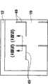
图1是表示适用本发明的显示装置的具体结构的框图。如图1所示,显示装置1是所谓的有源矩阵驱动方式的显示装置,作为基本结构具备有源矩阵驱动型的显示面板2和控制发光显示器1整体的控制器6。显示面板2具备:基板12(图4中示出),硼酸玻璃、石英玻璃、及其它玻璃等构成,对后述的晶体管的制造工序中的温度具有耐性;显示部7,设置在基板12上,具备多个象素,并且发光以显示按照来自控制器6的图像数据的图像;以及设置在基板12上并驱动显示部7的各象素用的选择扫描驱动器3、电压电源驱动器4和数据驱动器5。选择扫描驱动器3、电压电源驱动器4及数据驱动器5分别与控制器6连接,可输入来自控制器6的控制信号组φs、φe、φd和数据。在基板12上设置各种布线或元件,构成显示面板2。基板12的可见光透过率不一定要高。FIG. 1 is a block diagram showing a specific configuration of a display device to which the present invention is applied. As shown in FIG. 1 , the
在显示面板2中,在基板12上形成沿行方向彼此平行地排列的m条选择扫描线X1、X2、...、Xm。另外,沿行方向在基板12上形成相同数量的m条电压电源扫描线Z1、Z2、...、Zm,分别与选择扫描线X1、X2、...、Xm成组地交互排列。电压电源扫描线Z1、Z2、...、Zm与选择扫描线X1、X2、...、Xm彼此电绝缘。另外,沿与行方向正交的列方向在基板12上形成电流线Y1、Y2、...、Yn。另外,选择扫描线X1、X2、...、Xm和电压电源扫描线Z1、Z2、...、Zm可通过布图同一导电膜来同时形成。另外,电流线Y1、Y2、...、Yn设置成与选择扫描线X1、X2、...、Xm和电压电源扫描线Z1、Z2、...、Zm交叉,选择扫描线X1、X2、...、Xm和电压电源扫描线Z1、Z2、...、Zm通过后述的栅极绝缘膜23或半导体膜24等与电流线Y1、Y2、...、Yn绝缘。In the
将多个有机EL元件在基板12上排列成矩阵状,在被电流线Y1、Y2、...、Yn与选择扫描线X1、X2、...、Xm包围的各区域中,设置一个有机EL元件。并且,在该有机EL元件的周围设置用于规定电流流过一个有机EL元件中的驱动电路。一个有机EL元件和与之对应设置的驱动电路,对应于显示面板2的一象素。即在(m×n)个象素中分别设置一个有机EL元件。A plurality of organic EL elements are arranged in a matrix on the
下面,详细说明显示面板2。Next, the
在显示面板2内的显示部7中,将多个象素P1,1~Pm,n(m≥1、n≥2)设置成矩阵状。在第i行第j列的象素Pi,j(1≤i≤m、1≤j≤n)中,形成第i行第j列有机EL元件Ei,j和驱动有机EL元件Ei,j的第i行第j列象素驱动电路Di,j。象素驱动电路Di,j具备电容器17和分别作为n沟道非晶硅薄膜晶体管的第1晶体管8、第2晶体管9、第3晶体管10。In the
象素驱动电路Di,j的第1晶体管8的栅极电极8G连接于第i行的选择扫描线Xi上,漏极电极8D连接于第i行电压电源扫描线Zi上,源极电极8S连接于第3晶体管10的栅极电极10G上,同时连接于电容器17的一个极上。The
象素驱动电路Di,j的第2晶体管9的栅极电极9G连接于第i行的选择扫描线Xi上,漏极电极9D连接于第3晶体管10的源极电极10S上、且连接于电容器17的另一端上,源极电极9S连接于第j列电流线Yj上。The
象素驱动电路Di,j的第3晶体管10的栅极电极10G连接于第1晶体管8的源极电极8S和电容器17的一端上,其漏极电极10D连接于电压电源扫描线Zi上,源极电极10S与作为有机EL元件Ei,j的一个电极的象素电极连接、且连接于电容器17的另一个极上,进一步连接于第2晶体管9的漏极电极9D上。The
电容器17连接于第3晶体管10的栅极电极10G和源极电极10S之间,具有保持栅极电极10G与源极电极10S之间的电位的功能。The
有机EL元件Ei,j是在象素电极与对置电极13之间夹设有机EL层的结构,象素电极连接于第3晶体管10的源极电极10S上,向对置电极13施加基准电位Vss。The organic EL element Ei, j has a structure in which an organic EL layer is interposed between the pixel electrode and the
在显示部7中,如图2所示,在多个象素P1,1~Pm,n整个区域中,形成作为各有机EL元件E1,1~Em,n的对置电极的对置透明电极13。另外,设有与对置透明电极13接触的辅助电极层42。辅助电极层42具有电阻率比对置透明电极13的透明导电层13b低的导电性材料,具有降低与对置透明电极13合起来的电极的薄板阻抗的功能。另外,由于这种导电性材料对于可见光不透明,辅助电极层42在每个象素中形成开口部42a,在各开口部42a包围的区域中露出后述的有机EL层15和分别位于其两个面上的象素电极16以及对置透明电极13。因此,辅助电极层42覆盖有机EL元件E1,1-Em,n周围的选择扫描线X1~Xm、电流线Y1~Yn、和电压电源扫描线Z1~Zm。另外,为了消除象素驱动电路D1,1~Dm,n的第1晶体管8、第2晶体管9和第3晶体管10各自的源极电极、漏极电极中外来光反射产生的闪耀,辅助电极层42最好覆盖象素驱动电路Di,j的第1晶体管8、第2晶体管9和第3晶体管10。再者,若电容器17通过外来光进行反射,则最好同样被辅助电极层42覆盖。In the
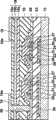
这里,详细说明象素Pi,j。图3是平面看象素Pi,j中的象素驱动电路Di,j的示意图,图4是沿图3的(IV)-(IV)线在厚度方向上切断时的剖面图,图5是沿图3的(V)-(V)线在厚度方向上切断时的剖面图,图6是沿图3的(VI)-(VI)线在厚度方向上切断时的剖面图。另外,图3中,为了便于理解,至少部分省略后述的栅极绝缘膜23、第一杂质半导体膜25、第二杂质半导体膜26、阻塞(block)绝缘膜36、对置透明电极13等。Here, the pixel Pi,j will be described in detail. Fig. 3 is the schematic diagram of the pixel drive circuit Di in the pixel Pi, j, and Fig. 4 is a cross-sectional view along the (IV)-(IV) line of Fig. 3 when cut in the thickness direction, and Fig. 5 is a sectional view taken along the line (V)-(V) in FIG. 3 in the thickness direction, and FIG. 6 is a sectional view taken in the thickness direction along the line (VI)-(VI) in FIG. 3 . In addition, in FIG. 3 , in order to facilitate understanding, the
在基板12上,以规定图案形成构成第1晶体管8的栅极电极8G、第2晶体管9的栅极电极9G、以及第3晶体管10的栅极电极10G的栅极电极层22。栅极电极层22是将与选择扫描线X1、X2、...、Xm、电压电源扫描线Z1、Z2、...、Zm相同的导电材料层同时布图而成的,另外,具有从铬、铝、铜、钛、钨或从其至少一部分中选择的合金等中选择的低阻抗材料。On the
在栅极电极层22上覆盖着阳极氧化有栅极电极层22的阳极氧化膜31,设置栅极绝缘膜23,以从阳极氧化膜31的上部覆盖显示部7的整个面。栅极绝缘膜23由氮化硅或氧化硅等具有透光性和绝缘性的材料构成。另外,栅极绝缘膜23还覆盖选择扫描线X1、X2、...、Xm和电压电源扫描线Z1、Z2、...、Zm。The
第1晶体管8、第2晶体管9和第3晶体管10的半导体膜24形成在分别经栅极绝缘膜23与各栅极电极层22对置的位置。该半导体膜24包含在从可见光到红外线波段的波段范围内具有分光灵敏度的本征非晶硅。在各半导体膜24上,形成保护半导体膜24的表面不被蚀刻液腐蚀的、由氮化硅构成的阻塞绝缘膜30。在各阻塞绝缘膜30的一侧部和另一侧部,分别彼此分隔地形成第一杂质半导体膜25和第二杂质半导体膜26。形成的各第一杂质半导体膜25覆盖半导体膜24的一侧部和阻塞绝缘膜30的一侧部地,形成的各第二杂质半导体膜26覆盖半导体膜24的另一侧部和阻塞绝缘膜30的另一侧部。第一杂质半导体膜25和第二杂质半导体膜26由掺杂了n型杂质离子的非晶硅构成。The
在各第1晶体管8、第2晶体管9和第3晶体管10的第一杂质半导体膜25上,形成构成漏极电极8D、漏极电极9D以及漏极电极10D的漏极电极层27,在各第1晶体管8、第2晶体管9和第3晶体管10的第二杂质半导体膜26上,形成构成源极电极8S、源极电极9S、以及源极电极10S的源极电极层28。漏极电极层27和源极电极层28是将与电流线Y1~Yn相同的导电材料层同时布图而成的,另外,具有从铬、铝、铜、钛、钨或从其至少一部分中选择的合金等中选择的低阻抗材料,并具有阻止可见光透过的功能。从而,抑制来自外部或各有机EL元件的光入射到半导体膜24、第一杂质半导体膜25和第二杂质半导体膜26中。源极电极层28与漏极电极层27通过彼此分隔来电绝缘。On the first
第1晶体管8、第2晶体管9、第3晶体管10除逆交错(stager)结构外,也可以是共面型,另外,也可以是至少其中之一为p沟道型晶体管,另外,除非晶硅外,也可以是多晶硅等晶体管。另外,为了防止各第1晶体管8、第2晶体管9和第3晶体管10的光恶化,基板12也可以具有遮光性。The
由氮化硅构成的保护绝缘膜29覆盖第1晶体管8、第2晶体管9、第3晶体管10、电容器17、选择扫描线X1、X2、...、Xm、电流线Y1、Y2、...、Yn、电压电源扫描线Z1、Z2、...、Zm。The protective
上述结构的第3晶体管10是将半导体膜24做为沟道区域的MOS型场效应晶体管。第1晶体管8和第2晶体管9的结构与上述的第3晶体管10实质上是相同的结构。另外,电容器17与第3晶体管10的栅极电极层22共用一个电极,与第3晶体管10的源极电极层28共用另一个电极。电容器17具有如下的电容器功能:通过将形成于一个电极和另一个电极之间的栅极绝缘膜23做为电介质,将随着流过第3晶体管10的源极-漏极间的电流的电流值变化而变化的第3晶体管10的栅极-源极间电位作为电荷数据储存。即,电容器17成为第3晶体管10的栅极-源极间的寄生电容,储存写入的电荷数据,之后,当向第3晶体管10的源极-漏极间施加规定电压时,保持积蓄在第3晶体管10的栅极-源极间的电荷,以便在第3晶体管10的源极-漏极间流过电流值与写入时相等的电流。The
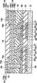
保护绝缘膜29上覆盖着由聚酰亚胺等构成的绝缘平坦化膜18。绝缘平坦化膜18用作在基板12的整个面上成膜的平坦化膜,由该绝缘平坦化膜18来消除第1晶体管8、第2晶体管9、第3晶体管10、...等上的保护绝缘膜29与基板12的表面上的保护绝缘膜29之间产生的阶差,绝缘平坦化膜18的表面构成大致平坦的面。该绝缘平坦化膜18由树脂(例如甲基丙烯酸树脂、丙烯树脂、环氧树脂)构成。并且,为了防止第1晶体管8、第2晶体管9、第3晶体管10、...的光恶化,例如也可混入炭黑等颜料,使绝缘平坦化膜18具有遮光性。The protective
在绝缘平坦化膜18上,在显示部7的整个面上形成光学干涉层19。光学干涉层19从绝缘平坦化膜18侧开始顺序层叠对来自上方的光进行镜面反射的反射层19a、设定成规定厚度和规定折射率的光透过性的透明层19b、具有半透半反镜功能的半反射层19c。光学干涉层19经光学设计有如下结构:对于可见光波段的光的反射率按反射层19a、半反射层19c、透明层19b的顺序变高,并且,对于可见光波段的光的透过率按透明层19b、半反射层19c、反射层19a的顺序变高。反射层19a是由Ag、Pt、Cu、Sn等金属或合金构成的、表面平滑且具有金属光泽的膜,透明层19b是氧化硅或氧化钛等电介质,可以是单层,但最好是多层。另外,这种光学干涉层19从平面看,最好构成对各色的每个象素组或每个象素独立的多个矩阵状来排列,以使形成与以后述的红、绿、蓝色之一分别发光的各有机EL元件的发光波长一致的光学膜厚。另外,光学干涉层19也可以是单层结构。On the insulating
另外,各第3晶体管10的漏极电极层27经设置在栅极绝缘膜23和阳极氧化膜31中的多个接触孔48连接于电压电源扫描线Z1、Z2、...、Zm的任一个上。In addition, the
各第1晶体管8的源极电极层28和第3晶体管10的栅极电极层22经设置在栅极绝缘膜23和阳极氧化膜31中的多个接触孔47连接。The
在光学干涉层19上形成有机EL元件E1,1~Em,n。有机EL元件E1,1~Em,n分别形成例如按用作阳极电极的象素电极16、若流过阈值以上的电流则发光的场致发光的EL层15、例如用作阴极电极的对置透明电极13的顺序层叠的层叠结构。The organic EL elements E1,1 toEm,n are formed on the
象素电极16经形成于绝缘平坦化膜18、光学干涉层19和保护绝缘膜29中的多个接触孔49同第3晶体管10的源极电极层28连接。The
其中,象素电极16在每个象素中彼此隔离且独立地形成,以被电分离,多个象素电极16从平面看排列成矩阵状。Among them, the
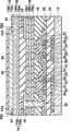
另外,在象素电极16周围的光学干涉层19上,与象素电极16的周缘部16a部分重合地设置有不沾液体的疏液性膜14。疏液性膜14设置开口部14a,使与象素电极16的中央部对应的位置开口,在该开口部14a内堆积EL层15。EL层15是由发光材料形成的层,是通过对从象素电极16注入的载流子(这里为空穴)与从对置透明电极13注入的载流子(这里为电子)进行再键合来发光的层。另外,象素P1,1~Pm,n的有机EL元件象素E1,1~Em,n的各EL层15是分别发出红、绿、蓝色光中之一的层,各色规则地排列。也可将发出同色光的EL层15排列在相同列中,也可将红、绿、蓝色的EL层15构成三角形排列。Also, on the
象素电极16对可见光具有透过性,同时具有导电性,只要能用作阳极,功函数越高越好。象素电极16例如由氧化铟、氧化锌、氧化锡或包含其中至少一个的混合物(例如氧化铟锡(ITO)、氧化铟锌、镉锡氧化物(CTO))形成。另外,也可通过将象素电极16作为半透半反镜来形成半反射层19c,但此时,相对可见光波段的光的反射率按反射层19a、象素电极16、透明层19b的顺序变高,并且,相对可见光波段的光的透过率按透明层19b、象素电极16、反射层19a的顺序变高。此时,透明层19b的光学膜厚为有机EL元件的EL层15发出的光的主波长(峰值波长)的2分之1的整数倍。另外,在不形成光学干涉层19的情况下,象素电极16也可不透明,最好对可见光波段的光具有反射性。The
可以在EL层15中适当混合利用电场来传输电子的电子传输性的物质,也可适当混合利用电场来传输空穴的空穴传输性的物质,或适当混合电子传输性的物质和空穴传输性的物质。即,EL层15可以是从象素电极16开始按空穴传输层、发光层、电子传输层的顺序层叠的三层结构,或是按空穴传输层、发光层的顺序层叠的二层结构,或是按发光层、电子传输层的顺序层叠的二层结构,或是由发光层构成的单层结构,或是在这些层结构中在适当的层间夹入电子或空穴的注入层的多层结构。另外,构成EL层15的所有层可以由有机化合物构成,构成EL层15的所有层也可以由无机化合物构成,EL层15也可以是层叠由无机化合物构成的层与由有机化合物构成的层而成。另外,在构成EL层15的所有层由无机化合物构成的情况下,有机EL元件是无机有机EL元件,在构成EL层15的层中存在由有机化合物构成的层的情况下,有机EL元件是有机EL元件。In the
在EL层15由低分子有机材料或无机物构成的情况下,可通过淀积法、溅射法等气相生长法来形成EL层15。另一方面,在EL层15例如由高分子有机材料构成的情况下,包含通过湿式成膜法在显示部7上成膜的高分子有机材料的有机化合物含有液由于与疏液性膜14的表面排斥,所以不形成于疏液性膜14上,可选择地成膜在对应于各象素P1,1~Pm,n的开口部14a内,即各象素电极16上。所谓有机化合物含有液是含有构成EL层15的有机化合物或其前驱体的液体,也可以是将构成EL层15的有机化合物或其前驱体作为溶质溶于溶媒中的溶液,或是将构成EL层15的有机化合物或其前驱体分散到分散媒中的分散液。When the
另外,EL层115的发光层中含有发光材料。作为发光材料,使用高分子类材料。作为高分子类材料,例如有聚咔唑类,聚对苯撑类,聚丙炔乙烯撑类,聚噻吩类,聚芴类,聚硅烷类,聚乙炔类,聚苯胺类,聚吡啶类,聚吡啶乙烯撑类,聚吡咯类材料。另外,作为高分子材料,可例举形成上述高分子材料(聚合物)的单体或是低聚物的聚合物或共聚物、单体或低聚物的衍生物的聚合物或共聚物、或者具有噁唑(噁二唑,三唑,二唑)或三苯胺骨架的单体进行聚合的聚合物或共聚物。另外,作为这些聚合体的单体,包含通过加热、加压、施加UV、电子线等来形成上述化合物的单体和前驱聚合体。另外,也可导入键合这些单体之间的非共役类单元。In addition, the light emitting layer of the EL layer 115 contains a light emitting material. As the light-emitting material, a polymer-based material is used. Examples of polymer materials include polycarbazoles, polyparaphenylenes, polypropyne vinylenes, polythiophenes, polyfluorenes, polysilanes, polyacetylenes, polyanilines, polypyridines, poly Pyridine vinylene, polypyrrole materials. In addition, examples of the polymer material include polymers or copolymers of monomers or oligomers forming the above-mentioned polymer materials (polymers), polymers or copolymers of derivatives of monomers or oligomers, Or polymers or copolymers of monomers with oxazole (oxadiazole, triazole, diazole) or triphenylamine skeletons. In addition, monomers of these polymers include monomers and precursor polymers that form the above-mentioned compounds by heating, pressurization, application of UV, electron beams, and the like. In addition, it is also possible to introduce a non-compatibility type unit which bonds between these monomers.
作为这种高分子材料的具体实例,例如有聚芴、聚乙烯基咔唑、聚十二烷基噻吩、聚乙烯羟噻吩、聚苯乙烯磺酸分散体改性物、聚9,9-二烷基芴、聚噻嗯基-9,9-二烷基噻吩、聚2,5-二烷基对苯撑噻嗯(二烷基:R=C1~C20)、聚对苯撑乙烯撑、聚2-甲氧基-5-(2’-乙基-己氧基)-对苯撑乙烯撑、聚2-甲氧基-5-(2’-乙基-戊氧基)-对苯撑乙烯撑、聚2,5-二甲基-对苯撑乙烯撑、聚2,5-噻嗯基乙烯撑、聚2,5-二甲基对苯撑乙烯撑、聚1,4-对苯撑氰基乙烯撑等。Specific examples of such polymer materials include polyfluorene, polyvinylcarbazole, polydodecylthiophene, polyethylene hydroxythiophene, polystyrenesulfonic acid dispersion modified products, poly9,9-bis Alkylfluorene, polythienyl-9,9-dialkylthiophene, poly-2,5-dialkyl-p-phenylene thiophene (dialkyl: R=C1~C20), poly-p-phenylene vinylene, Poly 2-methoxy-5-(2'-ethyl-hexyloxy)-p-phenylene vinylene, Poly 2-methoxy-5-(2'-ethyl-pentyloxy)-p-phenylene Vinylene,
另外,不限于高分子类材料,也可淀积低分子材料来成膜。另外,也可按照低分子材料的性质,在将低分子材料溶解在溶媒中的状态下涂布使用。并且,也可使低分子材料作为掺杂物分散到高分子聚合体中,作为对低分子材料进行聚合体分散时的聚合体,可根据状况来使用包含公知的通用聚合体的各种聚合体。In addition, not limited to high-molecular materials, low-molecular materials may also be deposited to form a film. In addition, depending on the properties of the low-molecular material, the low-molecular material may be coated and used in a state in which the low-molecular material is dissolved in a solvent. In addition, the low-molecular material can be dispersed in the high-molecular polymer as a dopant, and various polymers including known general-purpose polymers can be used depending on the situation as the polymer when the low-molecular material is polymer-dispersed. .
这里,EL层15是通过湿式成膜法形成的层,是按由作为导电性高分子的PEDOT(polythiophene:聚噻吩)和作为掺杂物的PSS(polystyrene sulfonate:聚苯乙烯磺酸)构成的空穴传输层115a、聚芴(polyfluorene)类发光材料构成的发光层115b的顺序层叠的二层结构。另外,在EL层15通过湿式成膜法来形成的情况下,期望在象素电极16上形成溶于液体、具有液体以40°以下的接触角浸湿的性质(下面称为亲液性。)的亲液性膜的状态下,在该亲液性膜上涂布有机化合物含有液体。Here, the
光学干涉层19的透明层19b的光学膜厚(层的厚度d×折射率n)是EL层15发出的光的主波长(峰值波长)的2分之1的整数倍。从而,光学干涉层19构成谐振结构。即,若EL层15发出的光、尤其是主波长附近的波段的光进入光学干涉层19内,则其中主波长的光在反射层19a与半反射层19c之间反复反射形成谐振,从光学干涉层19射向外部的光的强度变强。另一方面,在进入光学干涉层19内的外来光中被谐振的主波长以外的光,即使在反射层19a与半反射层19c之间反射时干涉,也由于相位与透明层19b的光学膜厚形成的光路长度不一致进而被衰减,所以基本上不会射到光学干涉层19以外。因此,因为光学干涉层19放大EL层15发出的光后,使较宽波段的光作为较窄波段射出,所以可提高各色的色纯度。此外,因为可抑制外来光的内部反射引起的闪耀,所以可进行较暗显示或黑显示,提高对比度。另外,期望透明层19b的光学膜厚对应于各象素的发光色的波段不同而不同,若各象素的发光色分别为R(红)、波长比红短的G(绿)、波长比绿短的B(蓝),则设定为象素R的透明层19b的光学膜厚>象素G的透明层19b的光学膜厚>象素B的透明层19b的光学膜厚。The optical film thickness (layer thickness d×refractive index n) of the
在各EL层15周围的光学干涉层19上,形成不沾液体、具有液体以50°以上的接触角浸湿的性质(下面称为疏液性。)的疏液性膜14(例如氟类树脂膜、反应性硅膜)。在平面看时,通过在EL层15间将疏液性膜14形成网格状,将由疏液性膜14围绕的多个围绕区域排列成矩阵状,在围绕区域内形成EL层15。如图4所示,疏液性膜14的一部分既可重叠也可不重叠在象素电极16的外缘的一部分上。特别是,EL层15非常薄地成膜,所以在通过湿式成膜法来形成EL层15的情况下,若相邻的象素中单方地流过有机化合物含有液体,则形成EL层15的厚度薄的象素,虽担心象素电极16与对置电极13短路,但由于疏液性膜14设在相邻的象素电极16之间,所以可防止流入相邻的象素中,而且,在相邻的象素是发出各不相同的颜色的光的不同材料的情况下,通过混合相邻象素的有机化合物含有液体,可防止各象素中的发光色的纯度降低。另外,疏液性膜14也可以是如下结构:在每个象素中使用未表现出疏液性的树脂等材料层,作为贮藏有机化合物含有液体的储藏部,在该材料层的露出表面上覆盖表现出疏液性的层。另外,在通过气相生长法来形成EL层15的情况下,也可不设置疏液性膜14。On the
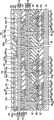
对置透明电极13作为所有象素P1,1~Pm,n的有机EL元件E1,1~Em,n的一方的共同电极而形成,在平面看形成于显示部7的大致整个区域中,是从EL层15侧按电子注入层13a、透明导电层13b的顺序层叠的层叠结构。电子注入层13a形成非常薄的、透过光的程度地,由功函数较低的材料(例如镁、钙、锂、钡或稀土类构成的单体金属或包含至少一种这些单体的合金)构成,其厚度比可见光波段薄,为10~200nm。透明导电层13b对可见光具有透过性,同时具有导电性,例如由氧化铟、氧化锌、氧化锡或包含其中至少一个的混合物(例如氧化铟锡(ITO)、氧化铟锌、镉锡氧化物(CTO))形成。这种材料的电阻率为100×10-6Ωcm~1000×10-6Ωcm左右。另外,为了提高对置透明电极13的光的透过率,期望将透明导电层13b做得较薄,其膜厚为50~1000nm。这样,对置透明电极13透过EL层15的发光波段的至少一部分,显示装置1是从对置透明电极13侧射出EL层15的光的所谓顶部发光结构。The opposing
对置透明电极13可以是分割成大于等于2个的多个电极,或者也可以是共同连接于在列方向上邻接的象素上的带状的多个电极,或是共同连接于在行方向上邻接的象素上的带状的多个电极。并且,在对置透明电极13上形成多个绝缘保护层41,大致对应于各EL层15成膜的区域。多个绝缘保护层41在平面看与EL层15一样,每个象素排列成独立的矩阵状。绝缘保护层41具有光透过性,例如由氧化硅(SiO2)和氮化硅(SiN)等无机硅化物或聚酰亚胺等有机树脂形成。The opposing
另外,在显示部7内的、位于绝缘保护层41的周缘部41a、41a之间的非显示区域中,形成导电性的辅助电极层42,在绝缘保护层41、41之间辅助电极层42直接连接在透明导电层13b上。辅助电极层42在平面看形成网格状,以便重叠在多个象素电极16、16彼此间的区域整体上,在由辅助电极层42的开口部42a包围的区域配置绝缘保护层41、EL层15、象素电极16和光学干涉层19。辅助电极层42的周缘部42b既可形成于对置透明电极13的周缘部的内侧,也可形成于其外侧,但为了降低薄板阻抗,辅助电极层42的占有面积最好尽可能接近显示部7内的整个非显示区域。绝缘保护层41的周缘部41a超出到辅助电极层42的开口部42a的外侧。因此,在通过蚀刻来布图辅助电极层42时,绝缘保护层41保护透明导电层13b不被蚀刻剂腐蚀。另外,使辅助电极层42位于与第1晶体管8、第2晶体管9和第3晶体管10平面看时重合的位置。In addition, in the non-display area located between the
辅助电极层42用作与对置透明电极13一体的电极,与对置透明电极13单体相比,可实现降低薄板阻抗的效果。辅助电极层42具有电阻率比透明导电层13b的材料低、且难以氧化的材料,在这点上最好是铜(电阻率为1.67×10-6Ωcm)、银(电阻率为1.59×10-6Ωcm)、金(电阻率为2.35×10-6Ωcm)、铂(电阻率为10.6×10-6Ωcm)、铝(电阻率为2.66×10-6Ωcm)、铬(电阻率为12.9×10-6Ωcm)、或包含其中至少之一的合金。另外,因为辅助电极层42与连接于第1晶体管8、第2晶体管9和第3晶体管10上的选择扫描线X1、X2、...、Xm、电流线Y1、Y2、...、Yn、以及电压电源扫描线Z1、Z2、...、Zm的配置位置在平面看时重叠,所以通过在辅助电极层42中使用低反射率的遮光材料,也可用作象素间的遮光膜(黑色掩模)。辅助电极层42的厚度为10nm~1000nm左右的厚度,为了提高遮光性最好为50nm以上。在选择扫描线X1、X2、...、Xm、电流线Y1、Y2、...、Yn、和电压电源扫描线Z1、Z2、...、Zm中的至少一个是由光反射性的导电材料构成的布线、且在平面看时光学干涉层19与由该光反射性的导电材料构成的布线不重叠的情况下,或者,在选择扫描线X1、X2、...、Xm、电流线Y1、Y2、...、Yn、和电压电源扫描线Z1、Z2、...、Zm中的至少一个是由光反射性的导电材料构成的布线、且在显示装置1上未设置光学干涉层19的情况下,辅助电极层42可抑制外来光在由反射性导电材料构成的布线中的反射,可提高识别性。此时,具体而言,辅助电极层42最好包含铬、铬氧化物、铬合金、镍钽合金、镍铜合金、其它镍合金中的至少一种。另外,也可在辅助电极层42的表面设置微小的凹凸,消除光泽,变为低反射率。另外,在不形成透明导电层13b的情况下,辅助电极层42在绝缘保护层41、41彼此之间最好直接连接于电子注入层13a上,另外,在未形成电子注入层13a的情况下,辅助电极层42在绝缘保护层41、41彼此之间最好直接连接于由透明导电层13b单体构成的对置透明电极13上。这样,在象素Pi,j的周围形成辅助电极层42,所以,可以较厚地堆积到不透明的程度,因此,可显著降低薄板阻抗。The
辅助电极层42具有电阻率比透明导电层13b低的材料,所以除实现降低EL层15上侧的电极的薄板阻抗的效果外,还因为不与透明导电层13b中位于显示区域的部分重合,所以在透明导电层13b的位于显示区域的部分中,EL层15的光可基本上不被辅助电极层42遮住地透过并射出到外侧。The
在没有辅助电极层42的情况下,对置透明电极13由于薄板阻抗高,对于与向对置透明电极13输出基准电位Vss的布线源接近的象素的对置透明电极13而言,在较远的象素的对置透明电极13中,对置透明电极13造成电压衰减,电流密度不均匀,发光亮度在面内分散,但通过使用辅助电极层42,可降低有机EL元件的电极的薄板阻抗,所以可不降低透过率而使流过各象素的对置透明电极13的电流的电流密度大致恒定,显示部7可均匀发光。In the absence of the
在辅助电极层42上,即在非显示区域中形成遮光膜44,遮光膜44与辅助电极层42一样在平面看时形成矩阵状,与辅助电极层42一致重叠。遮光膜44本身也可以不具备导电性,但具有透光性且反射率低。因此,遮光膜44设置成在平面看时使辅助电极层42与第1晶体管8、第2晶体管9、第3晶体管10、和选择扫描线X1、X2、...、Xm、电流线Y1、Y2、...、Yn、电压电源扫描线Z1、Z2、...、Zm的配置位置重叠,所以不仅抑制由此产生的光的反射,还形成反射光难以识别的结构。遮光膜44,可以是将例如炭黑等遮光性且低反射率的黑色颜料分散到树脂等母材(粘合剂)中来形成,也可以由遮光性且低反射率的树脂自身来形成,还可以是氧化铬等金属。此时,辅助电极层42也可以自身不具有遮光性及低反射率,辅助电极层42自身也可以具有遮光性、低反射率。The light-shielding
绝缘保护层41和遮光膜44上由密封膜43覆盖。密封膜43成膜在基板12的整个面上,密封膜43消除在绝缘保护层41与辅助电极层42之间产生的阶差,密封膜43的表面形成大致平坦的面。该密封膜43具有透光的性质,由透明的树脂(例如甲基丙烯酸合成树脂、丙烯树脂、环氧树脂)构成。The insulating
这里,不使象素电极16在平面看时与选择扫描线X1~Xm、电流线Y1~Yn及电压电源扫描线Z1~Zm的重合,是为了利用象素电极16和这些布线间的寄生电容来抑制流过这些布线的电流延迟,但若绝缘平坦化膜18厚度为可充分缓和寄生电容的程度,则也可不使象素电极16与这些布线重合,与此同时,由于象素电极16上的EL层也可以扩展,所以可增大显示面积或提高显示部7中的显示面积比例。Here, the
另外,必要时也可由玻璃基板来密闭密封膜43的上方。In addition, if necessary, the upper portion of the sealing
另外,显示装置1的象素驱动电路D1,1~Dm,n如后所述地是通过控制流过第3晶体管之一的信号电流的电流值来进行多灰度显示的电流灰度型,但不限于此,也可以是通过控制施加于象素驱动电路D1,1~Dm,n上的信号电压的电压值来进行多灰度显示的电压灰度型。In addition, the pixel drive circuits D1,1 to Dm,n of the
下面,说明显示装置1的制造方法。Next, a method of manufacturing the
(1)阵列基板的制造工序(1) Manufacturing process of array substrate
如图7A和图7B所示,在平板状的基板12的显示部7上,在各象素中形成第1晶体管8、第2晶体管9、第3晶体管10的同时,形成选择扫描线X1、X2、...、Xm、电流线Y1、Y2、...、Yn、电压电源扫描线Z1、Z2、...、Zm,之后,在这些晶体管8~10和布线X1~Xm、Y1~Yn、Z1~Zm上有选择地覆盖由氮化硅或氧化硅构成的保护绝缘膜29,并从其上开始在显示部7的整个区域中堆积由聚酰亚胺等树脂构成的绝缘平坦化膜18,之后,依次成膜反射层19a、透明层19b、半反射层19c,形成光学干涉层19。As shown in FIG. 7A and FIG. 7B, on the
(2)开口部的形成工序(2) Forming process of the opening
接着,如图8A和图8B所示,通过光刻在光学干涉层19、绝缘平坦化膜18和保护绝缘膜29上形成通到各象素的第3晶体管10的源极电极层28的多个接触孔49。绝缘平坦化膜18的开口部18a构成接触孔49的一部分。另外,在绝缘平坦化膜18的高度比象素电极16的厚度大的情况下,最好在成膜象素电极16之前,在开口部18a内埋入导电性材料。Next, as shown in FIGS. 8A and 8B , on the
(3)象素电极阵列的形成工序(3) Formation process of pixel electrode array
接着,如图9A和图9B所示,通过气相生长法在显示部7的一个面上形成光透过性的导电性膜(例如ITO膜),通过光刻胶法在该导电性膜上形成矩阵状的抗蚀剂,在利用抗蚀剂形成掩模的状态下,通过蚀刻法等来加工导电性膜的形状。之后,去除抗蚀剂。通过以上工序,残留的导电性膜构成通过接触孔49电连接于第3晶体管10的源极电极层28上的象素电极16,可将多个象素电极16布图成矩阵状。多个象素电极16按每个象素被配置由第1晶体管8、第2晶体管9和第3晶体管10包围的显示区域中,同时,彼此电分离,周缘部16a沿第1晶体管8、第2晶体管9和第3晶体管10形成。另外,在平面看时象素电极16重叠在光学干涉层19上,但在光透过性的导电性膜的腐蚀剂侵蚀光学干涉层19的情况下,也可使耐蚀刻性良好的绝缘层夹设在光学干涉层19与象素电极16之间。Next, as shown in FIGS. 9A and 9B , a light-transmitting conductive film (such as an ITO film) is formed on one surface of the
(4)疏液性膜的形成工序(4) Formation process of lyophobic film
接着,如图10A和图10B所示,在显示部7上网格状地形成具有使象素电极16的中央部露出的开口部14a的疏液性膜14。此时,规定疏液性膜14的开口部14a的周缘覆盖象素电极16的周缘部16a。疏液性膜14的形状也可通过光刻和蚀刻来形成。疏液性膜14也可以是具有含氟功能团的硅氮烷化合物等氟树脂膜或反应性硅膜,该硅氮烷化合物等氟树脂膜或反应性硅膜具有Si-N-Si键、且在N或/和Si中键合包含氟的功能团。Next, as shown in FIGS. 10A and 10B , the
另外,也可在显示部7的整个面上覆盖疏液性膜14,在象素电极16上面的疏液性膜14上重叠光触媒,该光触媒若接收规定波段的光,则产生促进使疏液性消失的化学反应的活性种(active species),通过从其上方入射规定波段的光,将应成膜EL层15的象素电极16上的疏液性膜14变为亲液性,如后所述,从其上开始成膜EL层15。具体而言,在显示部7的整体上薄薄地成膜含有硅氮烷化合物的液体,硅氮烷化合物成为聚合体后进行干燥,然后使氧化钛等光触媒配置在象素电极16上,选择性地向光触媒照射紫外线,使氟或含氟的功能团脱离象素电极16上的硅氮烷聚合体,消除疏液性膜14的疏液性,而位于象素电极16、16之间的疏液性膜14不被照射紫外线,以维持疏液性。此时,疏液性消失的疏液性膜14是绝缘膜,但因为极薄地成膜,所以即使形成于象素电极16上,也不会明显妨碍空穴或电子等载流子的注入。另外,也可以是疏液性膜14利用聚酰亚胺来形成以开口部14a为侧壁的基体,并在该基体的表面薄薄地覆盖例如氟等疏液性材料。In addition, it is also possible to cover the entire surface of the
(5)EL层的形成工序(5) Formation process of EL layer
接着,如图11A和图11B所示,在通过疏液性膜14的开口部14a露出的象素电极16上成膜EL层15。EL层15的布图也可使用喷出包含EL层15的构成材料的液体的液滴喷出喷嘴(喷墨喷嘴)来选择地堆积。即,使喷嘴面向放置在台上的基板12,使喷嘴相对基板12平行移动,同时,在喷嘴位于围绕区域上时,从喷嘴中喷出有机化合物含有液体。从而,可形成EL层15,以便在平面看时EL层15重叠在象素电极16上。Next, as shown in FIGS. 11A and 11B , an
这里,在EL层15由空穴传输层15a与发光层15b构成的情况下,首先空穴传输层用喷嘴向被疏液性膜14的各开口部14a包围的区域作为液滴喷出包含空穴传输层15a的构成材料的液体,该液体干燥后形成空穴传输层15a,之后,狭义的发光层用的喷嘴向被疏液性膜14的各开口部14a包围的区域喷出包含发光层15b的构成材料的液体,作为液滴,该液体干燥后形成发光层15b。即使空穴传输层15a或发光层15b含有的液滴多少滴落在疏液性膜14的边缘,也被疏液性膜14排斥液滴而容纳在周围被疏液性膜14包围的开口部(象素电极16)中。只要可通过疏液性膜14充分排斥液滴,则也可通过印刷来成膜EL层15。此时,即使印刷技术没有光刻那么好的精度,也由于疏液性膜14在相邻的象素之间隔开包含EL层15的构成材料的液体,所以可形成细间距的象素。Here, when the
另外,在基板12上设置网格状的金属掩模,以露出象素电极16,并在该状态下执行气相生长法,从而将EL层15成膜成矩阵状。另外,各象素的空穴传输层15a与发光层15b的发光色无关地也可以是相同材料的情况下,可以将显示部7整体浸入包含空穴传输层15a的构成材料的液体中,通过布图了的疏液性膜14来选择地形成于象素电极16上,或者,也可以不设置疏液性膜14,而将显示部7整体浸入包含空穴传输层15a的构成材料的液体中,将空穴传输层15a作为跨跃各象素而连续的层。In addition, a grid-shaped metal mask is provided on the
(6)对置透明电极的形成工序(6) Formation process of opposing transparent electrodes
接着,如图12A和图12B所示,在氩等惰性气体的气体介质(雰囲気)或1Torr以下的减压气体介质下,通过溅射法或淀积法,在显示部7的整体上覆盖10~200nm厚度的由镁、钙、锂、钡或稀土类构成的单体金属或包含至少一种以上这些单体的合金,形成电子注入层13a。接着,通过CVD等淀积法溅射法,在显示部7的整体上覆盖50~200nm厚度的从氧化铟锡(ITO)、氧化铟锌、镉锡氧化物(CTO)中选择的材料,在电子注入层13a上成膜透明导电层13b。Next, as shown in FIG. 12A and FIG. 12B , in a gas medium (atmosphere) of an inert gas such as argon or a reduced-pressure gas medium below 1 Torr, the
(7)绝缘保护层阵列的形成工序(7) Formation process of insulating protective layer array
接着,如图13A和图13B所示,通过依次执行气相生长法、光刻胶法、蚀刻法、抗蚀剂的去除,将多个透明的绝缘保护层41布图成矩阵状。这里,在平面看时,绝缘保护层41重叠形成在EL层15上。绝缘保护层41对可见光具有高的透过性,例如由氧化硅和氮化硅等无机硅化物或聚酰亚胺等有机树脂形成。另外,在绝缘保护层41由有机树脂构成的情况下,也可不依次执行气相生长法、光刻胶法、蚀刻法、抗蚀剂的去除,而通过应用液滴喷出技术(喷墨技术),直接将绝缘保护层41布图成矩阵状。Next, as shown in FIGS. 13A and 13B , a plurality of transparent insulating protection layers 41 are patterned into a matrix by sequentially performing vapor phase growth, photoresist, etching, and resist removal. Here, the insulating
(8)辅助电极层的形成工序(8) Formation process of auxiliary electrode layer
接着,如图14A和图14B所示,通过溅射等气相生长法,在显示部7中成膜从例如铜、银、金、铂、铝、铬或包含其中至少之一的合金中选择的遮光性的导电性膜,而且,在显示部7中成膜使炭黑分散到树脂中的遮光性树脂或氧化铬等遮光性金属,通过基于光刻的蚀刻来同时布图,从而形成辅助电极层42,并在其上方形成遮光膜44。辅助电极层42的电阻率最好为不大于50.0×10-6Ωcm,厚度最好为10nm~1000nm左右的厚度。在由辅助电极层42的开口部42a包围的区域中配置绝缘保护层41、EL层15、象素电极16和光学干涉层19,绝缘保护层41的周缘部41a超出到辅助电极层42的开口部42a的外侧,因此,在通过蚀刻来布图辅助电极层42时,绝缘保护层41保护透明导电层13b不被蚀刻剂腐蚀,另外,通过在较易被氧化的电子注入层13a的上方覆盖绝缘保护层41和透明导电层13b,由此,即使假设在绝缘保护层41和透明导电层13b中的一个中形成销孔,也可保护另一个,所以可防止被蚀刻剂氧化。另外,辅助电极层42和遮光膜44形成在平面看时与第1晶体管8、第2晶体管9、第3晶体管10、选择扫描线X1、X2、...、Xm、电流线Y1、Y2、...、Yn、电压电源扫描线Z1、Z2、...、Zm重叠的形状。另外,若遮光膜44是通过氧化辅助电极层42的导电性材料(例如铬)而成,则也可成膜辅助电极层42,并氧化其表面,由此作为遮光膜44。此时成膜的导电性材料的厚度包括事先由遮光膜44氧化的部分。另外,在导电性膜是铬膜的情况下,也可使用硝酸铈氨与高氯酸的混合液作为蚀刻液来进行湿式蚀刻法。Next, as shown in FIG. 14A and FIG. 14B, a film selected from, for example, copper, silver, gold, platinum, aluminum, chromium, or an alloy containing at least one of them is formed in the
(9)密封膜的形成工序(9) Formation process of sealing film
接着,如图15A和图15B所示,在显示部7中成膜形成在多个树脂薄膜间夹设金属薄膜、无机化合物层的透明密封膜43。此时,除选择扫描线X1~Xm、电流线Y1~Yn和电压电源扫描线Z1~Zm的各端子、及有机EL元件E1,1~Em,n的对置透明电极13的端子等从显示部7延伸到该区域外部的部分之外,最好尽可能覆盖显示部7内的构成材料。另外,为了平滑密封膜43的表面使EL层15的光高效射出,最好对密封膜43的表面进行化学研磨、机械研磨或机械化学研磨。另外,也可以在密封膜43的上方配置与基板12对置的对置基板,使显示部7配置在这些基板内。Next, as shown in FIGS. 15A and 15B , a
在如上所述地制造的显示装置1中,选择扫描驱动器3、电压电源驱动器4和数据驱动器5经选择扫描线X1~Xm、电流线Y1~Yn和电压电源扫描线Z1~Zm来控制各象素P1,1~Pm,n的象素驱动电路D1,1~Dm,n,有机EL元件E1,1~Em,n适当发光,从对置透明电极13侧向外部射出光。因此,对置透明电极13侧构成显示面,面向对置透明电极13侧的用户可看见显示内容。In the
如上所述,在本实施方式中,形成网格状的辅助电极层42直接形成在对置透明电极13上,以便重叠在多个象素电极16间的整个区域上,所以,即使对置透明电极13以较高的电阻率的金属氧化物材料等构成,也可降低电极整体的薄板阻抗,使电流容易流过,另外,因为由低阻抗的辅助电极层42来包围对置透明电极13的周围,所以可使对置透明电极13的电压在面内一样,故即使假设向全部象素电极16施加相同电位的情况下,流过的电流的电流值也变均匀,任一EL层15的发光强度都大致相等,可使面内的发光强度一样。As described above, in this embodiment, the grid-shaped
另外,由于较低阻抗的辅助电极层42充分降低电极整体的薄板阻抗,所以可进一步变薄对置透明电极13,抑制EL层15发出的光透过对置透明电极13时衰减的程度。这样,即使在低电压驱动下也能提供亮的显示画面,进而可抑制施加电压引起的EL层15的恶化,并实现显示装置1的长寿命化。In addition, since the
因为遮光性辅助电极层42在非显示区域中用作遮光膜,所以可提高对比度。另外,在光学干涉层19产生外来光的干涉作用,可降低入射到显示装置1的显示面的外来光的反射率,即使在显示装置1亮的环境下,也可抑制显示面的对比度下降。因此,用户容易看见显示装置1的显示画面。Since the light-shielding
下面,说明变形例。变形例的显示装置除以下说明的部分之外,其它结构与上述实施方式的显示装置1一样。Next, modified examples will be described. The configuration of the display device of the modified example is the same as that of the
(变形例1)(Modification 1)
在上述实施方式中,象素电极16是阳极,对置透明电极13是阴极,但如图16所示,也可以是象素电极16是阴极,对置透明电极13是阳极。此时,象素电极16是从基板12侧按透明导电层16d、电子注入层16e的顺序层叠的层叠结构。透明导电层16d、电子注入层16e在每个象素中独立形成,为矩阵状排列。透明导电层16d的特性、成分与上述实施方式中的透明导电层13b的一样,电子注入层16e的特性、成分与上述实施方式中的电子注入层13a的一样。透明导电层16d通过开口部18a连接于第3晶体管10的源极电极层28上。In the above-mentioned embodiment, the
此时,对置透明电极13是单层结构,该单层成膜在整个表面上。对置透明电极13的材料组成及特性与上述实施方式中的象素电极16相同。At this time, the opposing
另外,EL层15的层叠顺序与上述实施方式中的EL层15相反。即,在该变形例1中,EL层15是从象素电极16侧按发光层15b、空穴传输层15a的顺序层叠的结构。另外,EL层15也可以是从象素电极16开始按电子传输层、发光层、空穴传输层的顺序层叠的三层结构,或是按电子传输层、发光层的顺序层叠的二层结构,或是仅为发光层的单层结构。In addition, the stacking order of the EL layers 15 is reverse to that of the EL layers 15 in the above-mentioned embodiment. That is, in
在该变形例1的显示装置中,也可通过形成网格状的辅助电极层42来提高从对置透明电极13流过的电流的电流密度,同时,使电流密度在面内均匀。Also in the display device according to
(变形例2)(Modification 2)
在上述实施方式中,辅助电极层42形成于对置透明电极13上,但如图17所示,也可使辅助电极层42配置在对置透明电极13的下方。此时的辅助电极层42的平面看的位置与上述实施方式一样,如图3所示。在对置透明电极13形成之前,布图辅助电极层42,所以不必在对置透明电极13与辅助电极层42之间形成绝缘保护层41。另外,也可在对置透明电极13与辅助电极层42之间设置导电性的遮光膜44。In the above-mentioned embodiment, the
(变形例3)(Modification 3)
在上述各实施方式中,网格状地形成辅助电极层42,以使其重叠于象素电极16间的整个区域上,但如图18所示,也可将辅助电极层42成为分割成多个的带状。即,将在行方向(横向)上构成长条形成为带状的辅助电极层42直接连接在对置透明电极13上,以便连续配置在平面看时在行方向上相邻的多个象素电极16、16、...之间的周围。因此,各辅助电极层42与对置透明电极13一起使薄板阻抗降低,所以可使电压在面内一样,以便对于有机EL元件的电流密度 变均匀。另外,也可以使辅助电极层42在平面看时布与选择扫描线X1、X2、...、Xm、和电压电源扫描线Z1、Z2、...、Zm中的任一方重叠。为了抑制象素的开口率下降,期望辅助电极层42在平面看时尽可能不重叠象素电极16。In each of the above-mentioned embodiments, the
(变形例4)(Modification 4)
如图19所示,将列方向(纵向)上构成长条形的带状的多个辅助电极层42直接连接在对置透明电极13上,以便连续配置在平面看时在列方向上相邻的多个象素电极16、16、...之间的周围。因此,各辅助电极层42与对置透明电极13一起使薄板阻抗降低,所以可使电压在面内一样,以便对于有机EL元件的电流密度变均匀。另外,通过这种结构,也可使辅助电极层42在平面看时不与电流线Y1、Y2、...、Yn重叠。为了抑制象素的开口率下降,期望辅助电极层42在平面看时尽可能不重叠象素电极16。As shown in FIG. 19 , a plurality of auxiliary electrode layers 42 formed in a strip shape in the column direction (longitudinal direction) are directly connected to the opposite
(变形例5)(Modification 5)
在上述各实施方式中,在平面看时跨跃多个象素间连续形成辅助电极层42,但不限于此,如图20所示,也可在各象素的象素电极16的周围分别设置单独的辅助电极层42。另外,也可以使辅助电极层42在平面看时不与选择扫描线X1、X2、...、Xm、电流线Y1、Y2、...、Yn、电压电源扫描线Z1、Z2、...、Zm中的任一方重叠。为了抑制象素的开口率下降,期望辅助电极层42在平面看时尽可能不重叠象素电极16。In each of the above-mentioned embodiments, the
(变形例6)(Modification 6)
在上述实施方式中,在高阻抗的对置透明电极13中设置辅助电极层42来降低薄板阻抗,但在为了使象素电极16例如变为透明电极而适用金属氧化物并变为较高阻抗的情况下,如图21所示,也可以设置与象素电极16的周缘部16a局部重叠的象素电极用辅助电极层45。象素电极用辅助电极层45在每个象素中电气独立形成,某个象素的象素电极用辅助电极层45远离相邻的象素的象素电极用辅助电极层45。象素电极用辅助电极层45围绕对应的象素电极16形成为框状,并直接连接于对应的象素电极16上。在辅助电极层42的下方彼此相邻的象素电极用辅助电极层45,通过疏液性膜14来覆盖其上部。另外,在象素电极16的上面形成由疏液性膜14围绕周围的EL层15,在EL层15的上面跨跃多个象素来形成对置透明电极13。这里,当疏液性膜14在象素电极16与对置透明电极13之间不能表现出充分的绝缘性的情况下,也可覆盖氮化硅或聚酰亚胺等网格状的绝缘膜,并在其表面设置表现出疏液性的膜。另外,为了使整体厚度变薄,期望象素电极用辅助电极层45由电阻率比象素电极16低的材料构成,最好从铜、银、金、铂、铝、铬或包含其中至少之一的合金中选择。另外,象素电极用辅助电极层45的尺寸可以设计成宽度比辅助电极层42窄,以便从辅助电极层42的上方看时看不见象素电极用辅助电极层45,也可以设计成相同尺寸,使其与辅助电极层42完全重叠。另外,也可以不设置辅助电极层42而仅设置象素电极用辅助电极层45。In the above-mentioned embodiment, the
本发明不限于上述实施方式、上述变形例,在不脱离本发明要点的范围内,可进行各种改良和设计变更。The present invention is not limited to the above-mentioned embodiment and the above-mentioned modifications, and various improvements and design changes are possible without departing from the gist of the present invention.
在上述说明中,作为多个象素电极16的二维排列的一例,排列成矩阵状,但也可以将多个象素电极16排列成将相邻的RGB象素为分别作为顶点的三角形排列,或将象素形状设为六边形,排列成蜂窝状。另外,沿列方向排列由发出同色光的多个象素构成的象素组,这种象素组也可在行方向上与由发出不同色光的多个象素构成的象素组邻接。In the above description, as an example of a two-dimensional arrangement of a plurality of
另外,在上述说明中,在平面看时由辅助电极层42围绕的一个围绕区域中配置一个有机EL元件(即一个象素电极16与一个EL层15),但也可在一个围绕区域内配置多个有机EL元件。In addition, in the above description, one organic EL element (that is, one
下面,详细说明象素驱动电路Di,j的电路结构。Next, the circuit structure of the pixel driving circuit Di,j will be described in detail.
在非选择期间中施加于电压电源扫描线Zi的电压VNSE为基准电位Vss以上的电压,选择期间中施加于电压电源扫描线Zi的电压VSE小于等于基准电位Vss。例如,基准电位Vss是接地电位。The voltage VNSE applied to the voltage source scan line Zi during the non-selection period is a voltage higher than the reference potential Vss , and the voltage VSE applied to the voltage source scan line Zi during the selection period is less than or equal to the reference potential Vss . For example, the reference potential Vss is a ground potential.
如图1所示,选择扫描驱动器3连接于显示面板2的选择扫描线X1~Xm上。选择扫描驱动器3是所谓的移位寄存器。选择扫描驱动器3根据从控制器6输出的控制信号组Φs按从选择扫描线X1至选择扫描线Xm的顺序(选择扫描线Xm的下一个是选择扫描线X1)依次输出扫描信号,从而依次选择连接于各选择扫描线X1~Xm上的第1晶体管8、第2晶体管9。具体而言,选择扫描驱动器3在第1晶体管8、第2晶体管9是n沟道的情况下,选择地向选择扫描线X1~Xm施加高电平的导通电压VON(比基准电位Vss高)、或低电平的截止电压VOFF(与基准电位Vss相等的电位或比基准电位Vss低。)之一的选择扫描信号。即,在选择选择扫描线X1~Xm中的任一选择扫描线Xi的选择期间,选择扫描驱动器3向选择扫描线Xi输出导通电压VON的脉冲,从而,连接于选择扫描线Xi上的第2晶体管9、第3晶体管10(是从象素驱动电路Di,1至象素驱动电路Di,n的全部第2晶体管9、第3晶体管10。)变为导通状态,另一方面,在选择期间以外的非选择期间,通过向选择扫描线Xi施加截止电压VOFF,第2晶体管9、第3晶体管10变为截止状态。期望选择扫描线X1~Xm各自的选择期间不重合,但在连接于同一列的电流线Yj上的多个象素P以相同灰度发光的情况下,设定成同步选择扫描线X1~Xm的选择期间,且设定成同步电压电源扫描线Z1~Zm的选择期间。As shown in FIG. 1 , the
电压电源驱动器4连接于显示面板2的电压电源扫描线Z1~Zm上。电压电源驱动器4是所谓的移位寄存器。即,电压电源驱动器4根据从控制器6输出的控制信号组Φe按从电压电源扫描线Z1至电压电源扫描线Zm的顺序(电压电源扫描线Zm的下面是电压电源扫描线Z1)依次输出脉冲信号。具体而言,电压电源驱动器4以规定周期向各电压电源扫描线Z1~Zm施加与基准电位Vss相等的电位或比基准电位Vss低的选择电压(在基准电位为接地电位的时候,例如为0[V]。)。即,在选择选择扫描线X1~Xm中的任一选择扫描线Xi被选择的选择期间,电压电源驱动器4向电压电源扫描线Zi施加低电平的选择电压。另一方面,在非选择期间,电压电源驱动器4向电压电源扫描线Zi施加比基准电位Vss高的高电平的非选择电压VNSE。若该非选择电压VNSE比基准电位Vss高,则可以是负电压,但为了使第3晶体管10的源极-漏极间电压VDS达到饱和区,是充分大的值。后面详细描述饱和电压。The
控制器6根据输入的图像数据分别向选择驱动器3、电压电源驱动器4及数据驱动器5输出控制信号组φs、控制信号组φe、控制信号组φd。The
数据驱动器5是接受来自控制器6的控制信号组、并从各电流线Y1~Yn引入流向数据驱动器5的存储电流的电流吸收(sink)型驱动器。即,数据驱动器5具有电流吸收(sink)电路,如图22的箭头所示,在各电流线Y1~Yn中产生存储电流。在非选择期间中,有机EL元件E1,1~Em,n发光时流过的显示电流的电流值等于存储电流的电流值。数据驱动器5在选择期间中,使与该存储电流的电流值对应的大小的电荷积累在各电容器17中,作为电流数据。The data driver 5 is a current sink type driver that receives a control signal group from the
这里,说明数据驱动器5基于在各电流线Y1~Yn中流过规定电流值的存储的各象素P1,1~Pm,n的动作原理。Here, the principle of operation of the data driver 5 based on the stored pixels P1,1 to Pm,n in which a predetermined current value flows through the current lines Y1 to Yn will be described.
图24是表示作为n沟道型MOSFET的第3晶体管10的电流-电压特性的图。图24中,横轴是漏极-源极间的电压值,纵轴是漏极-源极间的电流值。在FET中,在图中的不饱和区、即源极-漏极间电压VDS小于依照栅极-源极间电压值VGS决定的漏极饱和阈值电压VTH的区域,若栅极-源极间电压值VGS恒定,则随着源极-漏极间电压VDS变大,源极-漏极间电流值IDS变大。另外,在图中的饱和区中,即在源极-漏极间电压VDS大于等于依照栅极-源极间电压值VGS的漏极饱和阈值电压VTH的区域中,若栅极-源极间电压值VGS恒定,则源极-漏极间电流值IDS大致恒定。FIG. 24 is a graph showing the current-voltage characteristics of the
饱和区中的栅极-源极间电流值IDS由如下的式1表示。The gate-source current value IDS in the saturation region is represented by
式1:Formula 1:
在上述式1中,μ是载流子(电子)的移动率,C0是将MOS结构的栅极绝缘膜作为电介质的电容,Z是沟道宽度,L是沟道长度。In the
另外,在图24中,栅极-源极间电压值VGS0-VGSMAX满足关系VGS0=0<VGS1<VGS2<VGS3<VGS4<VGSMAX。即,在漏极-源极间电压VDS恒定的情况下,随着栅极-源极间电压值VGS变大,无论是不饱和区还是饱和区,源极-漏极间电流值IDS都变大。再者,随着栅极-源极间电压值VGS变大,漏极饱和阈值电压VTH变大。In addition, in FIG. 24 , the gate-source voltage value VGS0 −VGSMAX satisfies the relationship VGS0 =0<VGS1 <VGS2 <VGS3 <VGS4 <VGSMAX . That is, when the drain-source voltage VDS is constant, as the gate-source voltage value VGS increases, the source-drain current value IDS all get bigger. Furthermore, as the gate-source voltage value VGS becomes larger, the drain saturation threshold voltage VTH becomes larger.
从上述可知,在不饱和区中,若源极-漏极间电压值VDS稍稍变化,则源极-漏极间电流值IDS变化,在饱和区中,若栅极-源极间电压值VGS恒定,则漏极-源极间电流值IDS唯一确定。这里,将第3晶体管10为栅极-源极间电压电平VGSMAX时的漏极-源极间电流水平IDS,被设定成以最大亮度发光的有机EL元件Ei,j的象素电极16与对置电极13之间流过的电流水平。It can be seen from the above that in the unsaturated region, if the voltage value VDS between the source and drain changes slightly, the current value IDS between the source and drain changes. In the saturated region, if the voltage value between the gate and the source changes When VGS is constant, the current value IDS between the drain and the source is uniquely determined. Here, the drain-source current level IDS when the
下面,用图25的时序图来说明上述结构的象素驱动电路Di,j的动作、象素驱动电路Di,j的驱动方法和显示装置1的动作。图25中,TSE的期间是选择期间,TNSE的期间是非选择期间,TSC的期间是一个扫描期间。另外,有TSC=TSE+TNSE。Next, the operation of the pixel driving circuit Di,j configured as above, the driving method of the pixel driving circuit Di,j and the operation of the
按照从控制器6输出的控制信号组φs,选择扫描驱动器3从第1行的选择扫描线X1向第m行的选择扫描线Xm依次输出高电平(导通电位)的脉冲。另外,按照从控制器6输出的控制信号组φe,电压电源驱动器4从第1行的电压电源扫描线Z1向第m行的电压电源扫描线Zm依次输出低电平的脉冲。According to the control signal group φs output from the
这里,如图25所示,在各行中输出选择扫描线Xi的高电平电压的定时基本上与输出电压电源扫描线Zi的低电平脉冲的输出定时一致,选择扫描线Xi的高电平电压与电压电源扫描线Zi的低电平电压的时间长度基本相同。输出高电平的脉冲和低电平的脉冲的期间是该行的选择期间TSE。另外,在各行的选择期间TSE中,数据驱动器5按照从控制器6输出的控制信号组φd在所有列的电流线Y1~Yn中产生存储电流(即流向数据驱动器5的电流)。这里,数据驱动器5以控制器6接受的图像数据决定的电流值,在各列的电流线Yj中流过存储电流。Here, as shown in FIG. 25, the timing of outputting the high-level voltage of the selected scanning line Xi in each row basically coincides with the output timing of the low-level pulse of the output voltage power supply scanning line Zi , and the timing of outputting the high-level voltage of the selected scanning lineXi The time length of the high-level voltage is basically the same as that of the low-level voltage of the voltage supply scan lineZi . The period during which a high-level pulse and a low-level pulse are output is the selection period TSE of the row. In addition, in the selection period TSE of each row, the data driver 5 generates storage currents (that is, currents flowing to the data driver 5 ) in the current lines Y1 -Yn of all columns according to the control signal group φd output from the
详细说明象素Pi,j的电流的流动和电压的施加。The flow of current and the application of voltage to pixels Pi, j will be described in detail.
在第i行的选择期间TSE的开始时刻t1,从选择扫描驱动器3向第i行的选择扫描线Xi输出导通电位(高电平)的电压,在时刻t1~时刻t2的选择期间TSE,向选择扫描线Xi施加使第1晶体管8和第2晶体管变为导通状态的扫描信号电压VCN。再者,在第i行的选择期间TSE,向电压电源扫描线Zi施加与基准电位Vss相等的电位或比基准电位Vss低的选择电压VSE。而且,在选择期间TSE中,数据驱动器5根据控制器6接受的图像数据,流过规定电流值的存储电流。At the start time t1 of the selection period TSE of the i-th row, the
因此,在选择期间TSE中,第1晶体管8导通,从漏极向源极流过电流,向第3晶体管10的栅极和电容器17的一端施加电压,第3晶体管10导通。另外,在选择期间TSE中,第2晶体管9导通,数据驱动器5在电流线Y1、Y2、…、Yj、Yj+1、…、Yn中流过对应于图像数据的存储电流。此时,数据驱动器5为了在电流线Y1、Y2、…、Yj、Yj+1…、Yn中流过存储电流,使电流线Y1、Y2、…、Yj、Yj+1、…、Yn成为选择电压VSE以下、且基准电压Vss以下,将第3晶体管10的源极10S的电位设得比漏极的电位低。Therefore, in the selection period TSE , the
而且,因为在第3晶体管10的栅极-源极间产生电位差,所以如图22所示,在电流线Y1、Y2、…、Yj、Yj+1、…、Yn中沿箭头α所示方向分别流过由数据驱动器5指定的电流值(即对应于图像数据的电流值)的存储电流I1、I2、…、Ij、Ij+1…、In。另外,在选择期间TSE中,因为电压电源扫描线Zi的选择电压VSE为基准电压Vss以下,所以有机EL元件Ei,j的阳极电位比阴极电位低,向有机EL元件Ei,j施加逆偏压。因此,在有机EL元件Ei,j中不流过来自电压电源扫描线Zi的电流。Furthermore, sincea potential differenceis generated between the gate and the source of the
此时,象素Pi,1~象素Pi,n的各电容器17的另一端(连接于第3晶体管10的源极电极10S上。)成为与由数据驱动器5控制(指定)的电流值对应的电位,并且,变为比第3晶体管10的栅极电位低的电位。即,向各象素Pi,1~象素Pi,n的各电容器17存储电荷,产生可在各象素Pi,1~象素Pi,n的第3晶体管10中分别流过电流I1~In的、各第3晶体管10的栅极-源极间电位差。At this time, the other end (connected to the
这里,从第3晶体管10到电流线Yi的布线等任意点上的电位,随着第2晶体管9~第3晶体管10的随时间变化的内部阻抗等而不同。但是,由于通过数据驱动器5的电流控制而流过的电流表示规定的电流值,所以通过使第2晶体管9~第3晶体管10的阻抗成为高阻抗,即使第3晶体管10的栅极-源极间的电位变化,向箭头α所示方向流动的电流的规定电流值不会变化。Here, the potential at an arbitrary point such as the wiring from the
在选择期间TSE的终止时刻t2,从选择扫描驱动器3输出到选择扫描线Xi的高电平脉冲终止,从电压电源驱动器4输出到电压电源扫描线Zi的低电平脉冲终止。即,在从该终止时刻t2到下次的选择期间TSE的开始时刻t1的非选择期间TNSE中,向选择扫描线Xi中第1晶体管8的栅极和第2晶体管9的栅极施加截止电平(低电位)的扫描信号电压VOFF,并且,向电压电源扫描线Zi施加比基准电位Vss高得多的非选择电压VNSE。因此,如图23所示,在非选择期间TNSE中,第2晶体管9变为截止状态,在电流线Y1~Yn中不流过电流。并且,在非选择期间中TNSE中,第1晶体管8变为截止状态。At the end timet2 of the selection period TSE , the high-level pulse output from the
因为有机EL元件Ei,j不能避免从长时间看缓慢高阻抗化的随时间恶化,所以有机EL元件Ei,j的分压会缓慢变高,在施加恒定电压的情况下,担心施加于串联在有机EL元件Ei,j上的晶体管的电压会在晶体管中相对变低。这里,若将有机EL元件Ei,j在发光寿命期间以最大亮度发光时所需的有机EL元件Ei,j的最大内部电压设为VE,则在选择期间TSE后的非选择期间TNSE,如图24所示,即使第3晶体管10的栅极-源极度间电压VGS为VGSMAX,但为了使第3晶体管10的源极度-漏极间维持饱和区,即为了不依赖于第3晶体管10的源极-漏极间电压VDS、而仅通过第3晶体管10的栅极-源极间电压VGS来控制第3晶体管10的源极-漏极电流IDS,需满足下述所示条件式2。Since the organic EL element Ei,j cannot avoid the deterioration over time of slowly high impedance in the long run, the divided voltage of the organic EL element Ei,j will gradually increase, and there is a concern that the voltage applied to the The voltage of the transistor connected in series to the organic EL element Ei, j becomes relatively low among the transistors. Here, if the maximum internal voltage of the organic EL element Ei,jrequired to emit light at the maximum brightness during the luminescence lifetime is VE , then in the non-selection period after the selection period TSE TNSE , as shown in FIG. 24 , even if the gate-source voltage VGS of the
式2:Formula 2:
VNSE-VE-Vss≥VTHMAXVNSE -VE -Vss ≥VTHMAX
VTHMAX是VGSMAX时的第3晶体管10的源极-漏极间的饱和阈值电压,考虑到伴随第3晶体管10随时间的恶化而引起的该饱和阈值的位移和显示面板2的多个第3晶体管10彼此的特性差异,当向第3晶体管10的栅极提供VGSMAX时,被设定成在第3晶体管10正常驱动的范围内预想为最高的电压。VTHMAX is the saturation threshold voltage between the source and the drain of the
电容器17在其一端和另一端,连续保持在选择期间TSE充电的电荷,第3晶体管10连续维持导通状态。即,在非选择期间TNSE与该非选择期间TNSE之前的选择期间TSE中,第3晶体管10的栅极-源极间电压值VGS相等。因此,第3晶体管10即使在非选择期间TNSE中也连续流过与选择期间TSE中依照图像数据的电流值的存储电流相等的显示电流,但因为第2晶体管9为截止状态,所以如上述式2所示,通过经有机EL元件Ei,j流向低电位的基准电压Vss,在有机EL元件Ei,j的象素电极16至对置透明电极13之间的有机EL层42中流过显示电流、即第3晶体管10的源极-漏极间电流IDS,有机EL元件Ei,j发光。The
这样,在选择期间TSE根据图像数据,数据驱动器5经电流线Yj强制地在第3晶体管10的源极-漏极之间流过存储电流,在非选择期间TNSE中,在有机EL元件Ei,j中流过与拉拔后的存储电流相等的显示电流,所以即使对于第3晶体管10的特性差异或随时间恶化引起的特性位移,第3晶体管10也可提供依照图像数据的期望的电流,并且,即使有机EL元件Ei,j随着时间推移阻抗变高,也由于在有机EL元件Ei,j中流过期望的电流,所以可进行稳定的亮度灰度显示。另外,在一个象素内,因为与有机EL元件Ei,j串联连接的晶体管构成为仅形成一个作为电流控制用晶体管的第3晶体管10,所以施加于电压电源扫描线Zi上的电压被分压的结构仅是有机EL元件Ei,j和第3晶体管10这两个,所以能够以低电压、进而低功耗驱动,同时,抑制象素内的晶体管数量,拓宽象素的发光区域的占有面积(开口率)。In this way, during the selection periodTSE , according to the image data, the data driver 5 forcibly flows the storage current between the source and the drain of the
若选择扫描线Xi的选择期间TSE终止,则接着开始选择扫描线Xi+1的选择期间TSE,与选择扫描线Xi一样地选择扫描驱动器3、电压电源驱动器4、数据驱动器5和控制器6动作。这样,按线顺序依次选择有机EL元件E1,1~E1,n、E2,1~E2,n、…、Em,1~Em,n,在选择扫描线X1~选择扫描线Xm的选择期间依次终止后,选择扫描线Xi的选择期间TSE再次开始。这样,在一个扫描期间TSC中,各象素发光的发光期间TEM实质上相当于非选择期间TNSE,随着选择扫描线的数量增大,发光期间TEM的时间可能变长。If the selection period TSE of the selected scan lineXi is terminated, then the selection period TSE of the selected scanline Xi+1 is started, and the
另外,对于一个象素Pi,j,可由三个第1晶体管8、第2晶体管9、第3晶体管10来实现基于电流控制的有源矩阵驱动方式的显示装置1,显示装置1的图像特性好。即,就控制电流值的有源矩阵驱动方式的显示装置1而言,在本发明中,可提高象素Pi,j的发光面积的比例,可对其它设计极限提供余裕。若发光面积的比例提高,则可使显示装置1的显示面的外观亮度变亮,另外,在以期望的外观亮度显示时,因为可使EL层15每单位面积中流过的电流值更小,所以可延长有机EL元件Ei,j的发光寿命。In addition, for one pixel Pi,j , the
另外,在选择期间TSE中,因为向有机EL元件Ei,j施加逆偏压,所以有机EL元件Ei,j的元件寿命延长。在上述实施方式中,各象素驱动电路Di,j的第1晶体管8、第2晶体管9、第3晶体管10全部是非晶硅构成半导体层的仅n沟道的单沟道型FET。因此,可在同一工序中同时在基板12上形成第1晶体管8、第2晶体管9、第3晶体管10,抑制显示面板2、显示装置1和象素驱动电路Di,j的制造所需的时间或成本的增大。另外,在第1晶体管8、第2晶体管9、第3晶体管10中也可采用p沟道型FET,可得到同样的效果。此时,图25所示的各信号都变为逆相位。In addition, in the selection period TSE , since the reverse bias voltage is applied to the organic EL elements Ei, j, the lifetime of the organic EL elements Ei,j is extended. In the above-mentioned embodiment, all of the
Claims (25)
Translated fromChineseApplications Claiming Priority (2)
| Application Number | Priority Date | Filing Date | Title |
|---|---|---|---|
| JP2003182489 | 2003-06-26 | ||
| JP2003182489AJP2005019211A (en) | 2003-06-26 | 2003-06-26 | EL display panel and method of manufacturing EL display panel |
Publications (2)
| Publication Number | Publication Date |
|---|---|
| CN1578571A CN1578571A (en) | 2005-02-09 |
| CN100585909Ctrue CN100585909C (en) | 2010-01-27 |
Family
ID=33535265
Family Applications (1)
| Application Number | Title | Priority Date | Filing Date |
|---|---|---|---|
| CN200410062038AExpired - Fee RelatedCN100585909C (en) | 2003-06-26 | 2004-06-28 | display device |
Country Status (5)
| Country | Link |
|---|---|
| US (1) | US7580014B2 (en) |
| JP (1) | JP2005019211A (en) |
| KR (1) | KR100698349B1 (en) |
| CN (1) | CN100585909C (en) |
| TW (1) | TWI263183B (en) |
Families Citing this family (64)
| Publication number | Priority date | Publication date | Assignee | Title |
|---|---|---|---|---|
| JP4020060B2 (en)* | 2003-08-29 | 2007-12-12 | 株式会社豊田自動織機 | Organic electroluminescence device |
| KR100552972B1 (en)* | 2003-10-09 | 2006-02-15 | 삼성에스디아이 주식회사 | Flat panel display and manufacturing method |
| JP4167651B2 (en)* | 2004-12-15 | 2008-10-15 | 東芝松下ディスプレイテクノロジー株式会社 | Display device |
| JP2006261058A (en)* | 2005-03-18 | 2006-09-28 | Sony Corp | Organic el element, display device, and manufacturing method of organic el element |
| JP4760080B2 (en)* | 2005-03-25 | 2011-08-31 | セイコーエプソン株式会社 | Method for manufacturing light emitting device |
| JP4742639B2 (en)* | 2005-03-25 | 2011-08-10 | セイコーエプソン株式会社 | Light emitting device |
| WO2006115283A1 (en)* | 2005-04-25 | 2006-11-02 | Showa Denko K. K. | Method of producing a display device |
| JP4449857B2 (en) | 2005-08-17 | 2010-04-14 | ソニー株式会社 | Manufacturing method of display device |
| JP2007059116A (en)* | 2005-08-23 | 2007-03-08 | Sony Corp | Display device |
| KR20070039433A (en)* | 2005-10-08 | 2007-04-12 | 삼성전자주식회사 | Display device |
| CN100511700C (en)* | 2005-11-14 | 2009-07-08 | 精工爱普生株式会社 | Emissive device and electronic apparatus |
| JP5076306B2 (en)* | 2005-11-14 | 2012-11-21 | セイコーエプソン株式会社 | LIGHT EMITTING DEVICE AND ELECTRONIC DEVICE |
| JP2007156388A (en)* | 2005-11-14 | 2007-06-21 | Seiko Epson Corp | LIGHT EMITTING DEVICE AND ELECTRONIC DEVICE |
| JP4513777B2 (en)* | 2005-11-14 | 2010-07-28 | セイコーエプソン株式会社 | LIGHT EMITTING DEVICE AND ELECTRONIC DEVICE |
| JP2007147814A (en)* | 2005-11-25 | 2007-06-14 | Seiko Epson Corp | LIGHT EMITTING DEVICE, ITS MANUFACTURING METHOD, AND ELECTRONIC DEVICE |
| JP5250960B2 (en)* | 2006-01-24 | 2013-07-31 | セイコーエプソン株式会社 | LIGHT EMITTING DEVICE AND ELECTRONIC DEVICE |
| US8477102B2 (en)* | 2006-03-22 | 2013-07-02 | Eastman Kodak Company | Increasing conductive polymer life by reversing voltage |
| JP2007287354A (en)* | 2006-04-12 | 2007-11-01 | Hitachi Displays Ltd | Organic EL display device |
| TW200808119A (en)* | 2006-06-28 | 2008-02-01 | Sumitomo Chemical Co | Organic electroluminescence device |
| JP2008034362A (en)* | 2006-06-28 | 2008-02-14 | Sumitomo Chemical Co Ltd | Organic electroluminescence device |
| US8053971B2 (en) | 2006-07-31 | 2011-11-08 | Lg Display Co., Ltd. | Organic light emitting device and method of fabricating the same |
| JP2008108530A (en)* | 2006-10-25 | 2008-05-08 | Hitachi Displays Ltd | Organic EL display device |
| JP5104274B2 (en)* | 2007-02-08 | 2012-12-19 | セイコーエプソン株式会社 | Light emitting device |
| US7728512B2 (en) | 2007-03-02 | 2010-06-01 | Universal Display Corporation | Organic light emitting device having an external microcavity |
| JP2008310974A (en)* | 2007-06-12 | 2008-12-25 | Casio Comput Co Ltd | Display device and manufacturing method thereof |
| JP2009032553A (en)* | 2007-07-27 | 2009-02-12 | Casio Comput Co Ltd | Display device |
| JP2009092908A (en)* | 2007-10-09 | 2009-04-30 | Canon Inc | Display device and manufacturing method thereof |
| JP2009122652A (en)* | 2007-10-23 | 2009-06-04 | Sony Corp | Display device and electronic device |
| JP5056420B2 (en)* | 2008-01-10 | 2012-10-24 | セイコーエプソン株式会社 | Organic EL panel and manufacturing method thereof |
| KR101432236B1 (en)* | 2008-08-26 | 2014-08-27 | 삼성디스플레이 주식회사 | Organic light emitting display |
| KR20100030865A (en)* | 2008-09-11 | 2010-03-19 | 삼성전자주식회사 | Organic light emitting device and the method thereof |
| KR100963074B1 (en)* | 2008-10-17 | 2010-06-14 | 삼성모바일디스플레이주식회사 | Organic light emitting display |
| KR100963075B1 (en)* | 2008-10-29 | 2010-06-14 | 삼성모바일디스플레이주식회사 | Organic light emitting display device |
| CN101728488B (en)* | 2008-10-30 | 2011-05-04 | 北京大学 | A kind of organic electroluminescence device and preparation method thereof |
| KR101084171B1 (en)* | 2009-08-10 | 2011-11-17 | 삼성모바일디스플레이주식회사 | Organic light emitting display device and manufacturing method of organic light emitting display device |
| WO2011027676A1 (en) | 2009-09-04 | 2011-03-10 | Semiconductor Energy Laboratory Co., Ltd. | Semiconductor device and manufacturing method thereof |
| TWI413441B (en)* | 2009-12-29 | 2013-10-21 | Au Optronics Corp | Pixel structure and electroluminescence device |
| US8154183B2 (en)* | 2010-03-04 | 2012-04-10 | General Electric Company | Mitigating shorting risks in encapsulated organic light emitting devices (OLEDs) |
| JP4941572B2 (en)* | 2010-03-31 | 2012-05-30 | カシオ計算機株式会社 | Semiconductor device, light emitting device, and electronic device |
| KR20120139386A (en)* | 2011-06-17 | 2012-12-27 | 삼성디스플레이 주식회사 | Organic light emitting display device |
| KR101521676B1 (en) | 2011-09-20 | 2015-05-19 | 엘지디스플레이 주식회사 | Organic light emitting diode display and method for manufacturing the same |
| US8912550B2 (en) | 2011-12-22 | 2014-12-16 | Sumitomo Electric Industries, Ltd. | Dislocations in SiC semiconductor substrate |
| US9252194B2 (en)* | 2012-02-01 | 2016-02-02 | Sharp Kabushiki Kaisha | Display device having a reflection of light reducing multilayer |
| JP5998626B2 (en)* | 2012-05-15 | 2016-09-28 | セイコーエプソン株式会社 | Electro-optical device and electronic apparatus |
| KR101407590B1 (en)* | 2012-11-19 | 2014-06-13 | 삼성디스플레이 주식회사 | Organic light emitting display device and the manufacturing method thereof |
| CN103022049B (en)* | 2012-12-12 | 2015-12-02 | 京东方科技集团股份有限公司 | Array base palte and preparation method thereof, display unit |
| WO2014181641A1 (en)* | 2013-05-09 | 2014-11-13 | 旭硝子株式会社 | Light-transmitting substrate, organic led element, and method for producing light-transmitting substrate |
| WO2015005346A1 (en)* | 2013-07-09 | 2015-01-15 | 日東電工株式会社 | Organic electroluminescent device, and refrigerator |
| JP6426402B2 (en)* | 2013-08-30 | 2018-11-21 | 株式会社半導体エネルギー研究所 | Display device |
| CN103456764B (en)* | 2013-09-09 | 2016-01-20 | 京东方科技集团股份有限公司 | OLED array and manufacture method, display unit |
| CN103700675A (en)* | 2013-12-31 | 2014-04-02 | 京东方科技集团股份有限公司 | AMOLED array substrate and display device |
| JP6577344B2 (en)* | 2015-11-18 | 2019-09-18 | 株式会社ジャパンディスプレイ | Display device and manufacturing method thereof |
| CN115458571A (en)* | 2016-01-21 | 2022-12-09 | 苹果公司 | Power and data routing structure for organic light emitting diode display |
| US9847351B2 (en)* | 2016-01-26 | 2017-12-19 | United Microelectronics Corp. | Semiconductor device and method for fabricating the same |
| JP2017174553A (en)* | 2016-03-22 | 2017-09-28 | 株式会社ジャパンディスプレイ | Display device |
| KR102608418B1 (en)* | 2016-07-13 | 2023-12-01 | 삼성디스플레이 주식회사 | Organic light emitting display apparatus |
| CN108666343B (en) | 2017-03-31 | 2019-08-30 | 京东方科技集团股份有限公司 | Display Substrates and Display Panels |
| US10319935B2 (en) | 2017-04-05 | 2019-06-11 | Joled Inc. | Organic EL display panel and method of manufacturing organic EL display panel |
| CN107977632B (en)* | 2017-12-05 | 2021-02-23 | 京东方科技集团股份有限公司 | Array substrate, display device and grain identification method thereof |
| US10627673B2 (en)* | 2018-04-06 | 2020-04-21 | Glo Ab | Light emitting diode array containing a multilayer bus electrode and method of making the same |
| TWI673544B (en)* | 2018-05-09 | 2019-10-01 | 友達光電股份有限公司 | Display panel and electronic device comprising thereof |
| KR20220006541A (en) | 2019-05-10 | 2022-01-17 | 가부시키가이샤 한도오따이 에네루기 켄큐쇼 | Display devices and electronic devices |
| CN115335761A (en)* | 2020-10-30 | 2022-11-11 | 京东方科技集团股份有限公司 | Display substrate, display panel and display device |
| TWI826076B (en)* | 2022-10-27 | 2023-12-11 | 友達光電股份有限公司 | Display device |
Family Cites Families (30)
| Publication number | Priority date | Publication date | Assignee | Title |
|---|---|---|---|---|
| JP3300065B2 (en) | 1992-11-13 | 2002-07-08 | パイオニア株式会社 | Organic electroluminescence device |
| US5796509A (en)* | 1996-08-21 | 1998-08-18 | International Business Machines Corporation | Thin film frontlighting and backlighting for spatial light modulators |
| JPH1092579A (en) | 1996-09-12 | 1998-04-10 | Sanyo Electric Co Ltd | Organic EL display |
| US5998805A (en)* | 1997-12-11 | 1999-12-07 | Motorola, Inc. | Active matrix OED array with improved OED cathode |
| JPH11224783A (en) | 1998-02-04 | 1999-08-17 | Toyota Central Res & Dev Lab Inc | Organic electroluminescence device |
| JP3203227B2 (en)* | 1998-02-27 | 2001-08-27 | 三洋電機株式会社 | Display device manufacturing method |
| JP3875401B2 (en) | 1998-05-12 | 2007-01-31 | Tdk株式会社 | Organic EL display device and organic EL element |
| JP2000003793A (en) | 1998-06-12 | 2000-01-07 | Casio Comput Co Ltd | EL device |
| DE69926598T2 (en) | 1998-07-24 | 2006-04-06 | Seiko Epson Corp. | DISPLAY DEVICE |
| JP2001035653A (en)* | 1999-07-21 | 2001-02-09 | Nec Corp | Organic EL panel and its filter |
| GB2353400B (en) | 1999-08-20 | 2004-01-14 | Cambridge Display Tech Ltd | Mutiple-wavelength light emitting device and electronic apparatus |
| JP4595143B2 (en)* | 1999-09-06 | 2010-12-08 | 双葉電子工業株式会社 | Organic EL device and manufacturing method thereof |
| JP2001102169A (en)* | 1999-10-01 | 2001-04-13 | Sanyo Electric Co Ltd | El display |
| JP4434411B2 (en)* | 2000-02-16 | 2010-03-17 | 出光興産株式会社 | Active drive type organic EL light emitting device and manufacturing method thereof |
| US6882102B2 (en)* | 2000-02-29 | 2005-04-19 | Semiconductor Energy Laboratory Co., Ltd. | Light emitting device and manufacturing method thereof |
| JP2002033185A (en) | 2000-05-06 | 2002-01-31 | Semiconductor Energy Lab Co Ltd | Light emitting devices and appliances |
| JP4713010B2 (en) | 2000-05-08 | 2011-06-29 | 株式会社半導体エネルギー研究所 | Light emitting device and manufacturing method thereof |
| JP2002108250A (en) | 2000-09-29 | 2002-04-10 | Sharp Corp | Active matrix drive type self-luminous display device and manufacturing method thereof |
| US6680570B2 (en) | 2001-03-21 | 2004-01-20 | Agilent Technologies, Inc. | Polymer organic light emitting device with improved color control |
| JP2002318556A (en)* | 2001-04-20 | 2002-10-31 | Toshiba Corp | Active matrix type flat display device and manufacturing method thereof |
| JP2002318553A (en) | 2001-04-20 | 2002-10-31 | Toshiba Corp | Self-luminous display |
| JP2003045674A (en) | 2001-08-02 | 2003-02-14 | Seiko Instruments Inc | Organic electroluminescent element |
| JP4058930B2 (en) | 2001-10-09 | 2008-03-12 | セイコーエプソン株式会社 | ORGANIC ELECTROLUMINESCENT DEVICE, ITS MANUFACTURING METHOD, AND ELECTRONIC DEVICE |
| JP3693051B2 (en)* | 2001-12-20 | 2005-09-07 | セイコーエプソン株式会社 | Electro-optical device, luminance design method for electro-optical device, luminance design program for electro-optical device, and electronic apparatus |
| JP4071652B2 (en)* | 2002-03-04 | 2008-04-02 | 株式会社 日立ディスプレイズ | Organic EL light emitting display |
| US7045861B2 (en)* | 2002-03-26 | 2006-05-16 | Semiconductor Energy Laboratory Co., Ltd. | Light-emitting device, liquid-crystal display device and method for manufacturing same |
| JP2003317971A (en)* | 2002-04-26 | 2003-11-07 | Semiconductor Energy Lab Co Ltd | Light emitting device and manufacturing method thereof |
| US6911772B2 (en)* | 2002-06-12 | 2005-06-28 | Eastman Kodak Company | Oled display having color filters for improving contrast |
| KR100504472B1 (en) | 2002-09-05 | 2005-08-04 | 엘지전자 주식회사 | organic electroluminescence device and fabricating method for the same |
| US6812637B2 (en) | 2003-03-13 | 2004-11-02 | Eastman Kodak Company | OLED display with auxiliary electrode |
- 2003
- 2003-06-26JPJP2003182489Apatent/JP2005019211A/enactivePending
- 2004
- 2004-06-14USUS10/867,630patent/US7580014B2/ennot_activeExpired - Fee Related
- 2004-06-22KRKR1020040046353Apatent/KR100698349B1/ennot_activeExpired - Fee Related
- 2004-06-25TWTW093118423Apatent/TWI263183B/ennot_activeIP Right Cessation
- 2004-06-28CNCN200410062038Apatent/CN100585909C/ennot_activeExpired - Fee Related
Also Published As
| Publication number | Publication date |
|---|---|
| TWI263183B (en) | 2006-10-01 |
| US7580014B2 (en) | 2009-08-25 |
| CN1578571A (en) | 2005-02-09 |
| KR20050001343A (en) | 2005-01-06 |
| KR100698349B1 (en) | 2007-03-23 |
| US20040263441A1 (en) | 2004-12-30 |
| JP2005019211A (en) | 2005-01-20 |
| TW200509017A (en) | 2005-03-01 |
Similar Documents
| Publication | Publication Date | Title |
|---|---|---|
| CN100585909C (en) | display device | |
| TWI843951B (en) | Display device and semiconductor device | |
| KR101477267B1 (en) | Light emitting element, light emitting device, manufacturing method of light emitting device, and sheet-like sealing material | |
| US8400055B2 (en) | Organic electroluminescence apparatus with metal auxiliary wiring | |
| KR101123089B1 (en) | Light emitting device, electronic device, and television device | |
| JP4541936B2 (en) | Flat panel display | |
| KR101004874B1 (en) | Display panel and manufacturing method | |
| KR100581913B1 (en) | Organic electroluminescent display | |
| JP4543798B2 (en) | Organic EL device and electronic device | |
| CN100514395C (en) | Display apparatus | |
| JP4339000B2 (en) | Semiconductor device and manufacturing method thereof | |
| US8076704B2 (en) | Organic light emitting device and manufacturing method thereof | |
| US10312473B2 (en) | Organic light emitting display device | |
| JP2004327215A (en) | Electro-optical device, substrate for electro-optical device, method of manufacturing electro-optical device, and electronic apparatus | |
| JP2005332616A (en) | Organic electroluminescence display device and electronic apparatus | |
| US11502147B2 (en) | Display device | |
| JP2007101713A (en) | Display device | |
| JP2000348860A (en) | Light emitting device | |
| KR100490536B1 (en) | Top emission type organic electro luminescence display device | |
| JP2005285977A (en) | Semiconductor device, electro-optical device and electronic apparatus | |
| KR20090109477A (en) | Organic EL device |
Legal Events
| Date | Code | Title | Description |
|---|---|---|---|
| C06 | Publication | ||
| PB01 | Publication | ||
| C10 | Entry into substantive examination | ||
| SE01 | Entry into force of request for substantive examination | ||
| C14 | Grant of patent or utility model | ||
| GR01 | Patent grant | ||
| C41 | Transfer of patent application or patent right or utility model | ||
| TR01 | Transfer of patent right | Effective date of registration:20170216 Address after:Irish Ross Kang Wangjun Patentee after:Soras OLED Address before:Tokyo, Japan Patentee before:CASIO Computer Corporation | |
| CF01 | Termination of patent right due to non-payment of annual fee | Granted publication date:20100127 Termination date:20210628 | |
| CF01 | Termination of patent right due to non-payment of annual fee |