CN100584155C - Substrate process for embedded components - Google Patents
Substrate process for embedded componentsDownload PDFInfo
- Publication number
- CN100584155C CN100584155CCN200710100549ACN200710100549ACN100584155CCN 100584155 CCN100584155 CCN 100584155CCN 200710100549 ACN200710100549 ACN 200710100549ACN 200710100549 ACN200710100549 ACN 200710100549ACN 100584155 CCN100584155 CCN 100584155C
- Authority
- CN
- China
- Prior art keywords
- layer
- circuit
- patterned circuit
- patterned
- solder mask
- Prior art date
- Legal status (The legal status is an assumption and is not a legal conclusion. Google has not performed a legal analysis and makes no representation as to the accuracy of the status listed.)
- Active
Links
- 239000000758substrateSubstances0.000titleclaimsabstractdescription48
- 238000000034methodMethods0.000titleclaimsabstractdescription21
- 239000010410layerSubstances0.000claimsabstractdescription422
- 239000012792core layerSubstances0.000claimsabstractdescription37
- 239000003292glueSubstances0.000claimsabstractdescription9
- 238000005429filling processMethods0.000claimsabstractdescription6
- 239000002184metalSubstances0.000claimsdescription61
- 229910052751metalInorganic materials0.000claimsdescription61
- 229910000679solderInorganic materials0.000claimsdescription53
- 238000004519manufacturing processMethods0.000claimsdescription43
- 230000003064anti-oxidating effectEffects0.000claimsdescription34
- PXHVJJICTQNCMI-UHFFFAOYSA-NNickelChemical compound[Ni]PXHVJJICTQNCMI-UHFFFAOYSA-N0.000claimsdescription6
- 238000005530etchingMethods0.000claimsdescription6
- 238000003475laminationMethods0.000claimsdescription6
- 238000001459lithographyMethods0.000claimsdescription6
- 239000000853adhesiveSubstances0.000claimsdescription4
- 230000001070adhesive effectEffects0.000claimsdescription4
- 238000009713electroplatingMethods0.000claimsdescription4
- 238000000059patterningMethods0.000claimsdescription4
- 238000003825pressingMethods0.000claimsdescription4
- 238000005229chemical vapour depositionMethods0.000claimsdescription3
- 238000007772electroless platingMethods0.000claimsdescription3
- PCHJSUWPFVWCPO-UHFFFAOYSA-NgoldChemical compound[Au]PCHJSUWPFVWCPO-UHFFFAOYSA-N0.000claimsdescription3
- 229910052737goldInorganic materials0.000claimsdescription3
- 239000010931goldSubstances0.000claimsdescription3
- 229910052759nickelInorganic materials0.000claimsdescription3
- 238000005240physical vapour depositionMethods0.000claimsdescription3
- 239000011248coating agentSubstances0.000claimsdescription2
- 238000000576coating methodMethods0.000claimsdescription2
- RYGMFSIKBFXOCR-UHFFFAOYSA-NCopperChemical compound[Cu]RYGMFSIKBFXOCR-UHFFFAOYSA-N0.000description6
- 239000000463materialSubstances0.000description6
- 238000010586diagramMethods0.000description5
- 238000005553drillingMethods0.000description5
- 229910052802copperInorganic materials0.000description4
- 239000010949copperSubstances0.000description4
- 238000007747platingMethods0.000description3
- 239000002344surface layerSubstances0.000description3
- 230000015572biosynthetic processEffects0.000description2
- 239000011889copper foilSubstances0.000description2
- 230000000694effectsEffects0.000description2
- 239000010408filmSubstances0.000description2
- 239000011521glassSubstances0.000description2
- -1polyethylene terephthalatePolymers0.000description2
- 229920000139polyethylene terephthalatePolymers0.000description2
- 239000005020polyethylene terephthalateSubstances0.000description2
- 239000011347resinSubstances0.000description2
- 229920005989resinPolymers0.000description2
- 229920002799BoPETPolymers0.000description1
- 239000003990capacitorSubstances0.000description1
- 239000004020conductorSubstances0.000description1
- 238000010438heat treatmentMethods0.000description1
- 230000000149penetrating effectEffects0.000description1
- 238000004382pottingMethods0.000description1
- 230000005855radiationEffects0.000description1
- 239000010409thin filmSubstances0.000description1
Images


Landscapes
- Production Of Multi-Layered Print Wiring Board (AREA)
Abstract
Description
Translated fromChinese技术领域technical field
本发明是有关于一种基板制程,且特别是有关于一种内埋元件的基板制程。The present invention relates to a substrate manufacturing process, and in particular to a substrate manufacturing process of embedded components.
背景技术Background technique
一般而言,线路基板主要是由多层图案化线路层(patterned circuitlayer)及介电层(dielectric layer)交替叠合所构成。其中,图案化线路层是由铜箔层(copper foil)经过微影与蚀刻制程定义形成,而介电层配置于图案化线路层之间,用以隔离两相邻的图案化线路层。此外,相邻的图案化线路层之间是透过贯穿介电层的导电通孔(plating through hole,PTH)或导电孔道(conductive via)而彼此电性连接。最后,在线路基板的表面配置各种电子元件(例如主动元件或被动元件),并通过内部线路的电路设计而达到电子信号传递(electrical signal propagation)的目的。Generally speaking, a circuit substrate is mainly composed of multiple layers of patterned circuit layers and dielectric layers laminated alternately. Wherein, the patterned circuit layer is defined by a copper foil layer (copper foil) through lithography and etching processes, and the dielectric layer is arranged between the patterned circuit layers to isolate two adjacent patterned circuit layers. In addition, adjacent patterned circuit layers are electrically connected to each other through plating through holes (PTH) or conductive vias penetrating the dielectric layer. Finally, arrange various electronic components (such as active components or passive components) on the surface of the circuit substrate, and achieve the purpose of electrical signal propagation through the circuit design of the internal circuit.
然而,随着市场对于电子产品应具有轻薄短小且携带方便的需求,因此在目前的电子产品中,将原先焊接于线路基板表面的电子元件设计为可埋设于线路基板的内部的一内埋元件,这样可以增加线路基板表面的布线面积,以达到电子产品薄型化的目的。However, as the market demands that electronic products should be thin, light, small and portable, in current electronic products, the electronic components that were originally soldered on the surface of the circuit substrate are designed as an embedded component that can be buried inside the circuit substrate. , which can increase the wiring area on the surface of the circuit substrate to achieve the purpose of thinning electronic products.
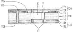
图1A至图1E为现有的一种内埋元件的基板制程的制作流程剖面示意图。首先,请参考图1A,提供一核心层110,核心层110具有一第一介电层112、一第一图案化线路层114,以及一第二图案化线路层116。第一图案化线路层114与第二图案化线路层116分别位于第一介电层112的一上表面112a与一下表面112b。FIGS. 1A to 1E are cross-sectional schematic diagrams of a manufacturing process of a conventional substrate manufacturing process for embedded components. First, please refer to FIG. 1A , a
接着,请参考图1B,在核心层110中形成一贯孔(through hole)H1并且将一内埋元件E放置于贯孔H1中,其中内埋元件E具有两电极E1。接着,请参考图1C,将一第一叠合层120与一第二叠合层130分别配置于第一图案化线路层114与第二图案化线路层116上,其中,第一叠合层120包括一第一金属层122及一第二介电层124,第二叠合层130包括一第二金属层132及一第三介电层134,且第二介电层124与第三介电层134分别朝向第一图案化线路层114与第二图案化线路层116。Next, please refer to FIG. 1B , a through hole H1 is formed in the
再者,请参考图1D,压合第一叠合层120、核心层110与第二叠合层130,并且形成至少一导电通孔H2与多个导电孔道V。其中,导电通孔H2贯穿第一叠合层120、核心层110与第二叠合层130,使得第一金属层122与第二金属层132可透过导电通孔H2彼此电性连接。此外,内埋元件E的两电极E1可透过这些导电孔道V分别与第一金属层122及第二金属层132电性连接。Furthermore, referring to FIG. 1D , the first laminated
最后,请参考图1D与图1E,图案化第一金属层122与第二金属层132,以分别形成一第一表层线路122’与一第二表层线路132’,并通过导电通孔H2电性导通第一表层线路122’与第二表层线路132’,且通过这些导电孔道V使得内埋元件E的两电极E1分别与第一表层线路122’及第二表层线路132’电性连接。通过这种方式完成内埋元件的基板制程的制作流程。Finally, referring to FIG. 1D and FIG. 1E , the
然而,现有内埋元件的基板制程中的内埋元件E必须经由这些导电孔道V而电性连接至第一表层线路122’与第二表层线路132’,这样会降低第一图案化线路层114与第二图案化线路层116的布线面积,进而降低第一图案化线路层114与第二图案化线路层116的布线密度。此外,内埋元件E需透过导电孔道V与第一表层线路122’与第二表层线路132’电性连接,然而,这种方式将会增加整个线路基板的厚度,而无法符合轻薄短小的产品设计要求。因此现有的内埋元件的基板制程实有改进的必要。However, the embedded element E in the substrate manufacturing process of the existing embedded element must be electrically connected to the
发明内容Contents of the invention
本发明的主要目的在于提供一种内埋元件的基板制程,以提升第一图案化线路层、第二图案化线路层、第一表层线路与第二表层线路的布线密度,并可有效地减少整个基板的厚度。The main purpose of the present invention is to provide a substrate manufacturing process for embedded components to increase the wiring density of the first patterned circuit layer, the second patterned circuit layer, the first surface circuit and the second surface circuit, and effectively reduce the The thickness of the entire substrate.
为达成上述目的或是其它目的,本发明采用如下技术方案:一种内埋元件的基板制程,其包括下列步骤:步骤(a)是提供一核心层,所述核心层具有一第一介电层、一第一图案化线路层及一第二图案化线路层,所述第一图案化线路层与所述第二图案化线路层分别位于所述第一介电层的一上表面与一下表面;步骤(b)是在所述核心层中形成一贯孔;其特征在于:所述基板制程还包括有下列步骤:步骤(c)是将所述核心层配置在一支撑板上,且将一内埋元件置放在所述贯孔中,其中所述内埋元件具有至少一电极;步骤(d)是进行一灌胶制程,使所述内埋元件固定在所述贯孔中;步骤(e)是移除所述支撑板;以及步骤(f)是电性连接所述内埋元件的所述电极与所述第二图案化线路层。In order to achieve the above object or other objects, the present invention adopts the following technical solution: a substrate manufacturing process for embedded components, which includes the following steps: step (a) is to provide a core layer, the core layer has a first dielectric Layer, a first patterned circuit layer and a second patterned circuit layer, the first patterned circuit layer and the second patterned circuit layer are respectively located on an upper surface and a lower surface of the first dielectric layer surface; step (b) is to form a through hole in the core layer; it is characterized in that: the substrate manufacturing process also includes the following steps: step (c) is to arrange the core layer on a support plate, and An embedded component is placed in the through hole, wherein the embedded component has at least one electrode; step (d) is to perform a glue filling process, so that the embedded component is fixed in the through hole; step (e) is removing the support plate; and step (f) is electrically connecting the electrode of the embedded element with the second patterned circuit layer.
在本发明的一实施例中,上述提供核心层的步骤(a)包括:利用微影及蚀刻制程分别图案化位于第一介电层的上表面及下表面的一第一金属层与一第二金属层,以在第一介电层的上表面及下表面上形成第一图案化线路层与第二图案化线路层。In one embodiment of the present invention, the step (a) of providing the core layer includes: patterning a first metal layer and a first metal layer located on the upper surface and the lower surface of the first dielectric layer respectively by using lithography and etching processes. Two metal layers are used to form a first patterned circuit layer and a second patterned circuit layer on the upper surface and the lower surface of the first dielectric layer.
在本发明的一实施例中,上述提供核心层的步骤(a)包括:利用微影及蚀刻制程分别图案化位于第一介电层的上表面及下表面的一第一金属层与一第二金属层,以在第一介电层的上表面及下表面上形成第一图案化线路层与第二图案化线路层。此外,第一金属层与第二金属层的材质包括铜。In one embodiment of the present invention, the step (a) of providing the core layer includes: patterning a first metal layer and a first metal layer located on the upper surface and the lower surface of the first dielectric layer respectively by using lithography and etching processes. Two metal layers are used to form a first patterned circuit layer and a second patterned circuit layer on the upper surface and the lower surface of the first dielectric layer. In addition, the material of the first metal layer and the second metal layer includes copper.
在本发明的一实施例中,上述形成贯孔的方式包括机械钻孔或雷射成孔。In an embodiment of the present invention, the above-mentioned method of forming through holes includes mechanical drilling or laser forming.
在本发明的一实施例中,上述支撑板可为一玻璃板或是一聚对苯二酸乙烯酯膜(PET film)。In an embodiment of the present invention, the above-mentioned support plate can be a glass plate or a polyethylene terephthalate film (PET film).
在本发明的一实施例中,上述内埋元件包括主动元件及被动元件。In an embodiment of the present invention, the embedded components include active components and passive components.
在本发明的一实施例中,上述灌胶制程例如是将一黏着剂填充于内埋元件与贯孔之间的间隙中。In an embodiment of the present invention, the above glue filling process is, for example, filling an adhesive in the gap between the embedded component and the through hole.
在本发明的一实施例中,上述电性连接内埋元件的电极与第二图案化线路层的步骤(f)包括有以下步骤:首先,在第二图案化线路层上配置一屏蔽,屏蔽暴露出电极与部分第二图案化线路层;接着,在第一介电层的下表面形成一金属层,其中部分金属层是电性连接电极与第二图案化线路层;再接着,移除屏蔽。In an embodiment of the present invention, the step (f) of electrically connecting the electrode of the embedded component with the second patterned circuit layer includes the following steps: first, a shield is arranged on the second patterned circuit layer, and the shield exposing the electrode and part of the second patterned circuit layer; then, forming a metal layer on the lower surface of the first dielectric layer, wherein part of the metal layer is electrically connected to the electrode and the second patterned circuit layer; and then, removing shield.
在本发明的一实施例中,上述电性连接内埋元件的电极与第二图案化线路层的步骤(f)包括有以下步骤:首先,在第二图案化线路层上配置一屏蔽,屏蔽暴露出电极与部分第二图案化线路层;接着,在第一介电层的下表面形成一金属层,其中部分金属层是电性连接电极与第二图案化线路层;再接着,移除屏蔽。此外,形成金属层的方法包括电镀、无电镀、物理气相沉积法或化学气相沉积法。In an embodiment of the present invention, the step (f) of electrically connecting the electrode of the embedded component with the second patterned circuit layer includes the following steps: first, a shield is arranged on the second patterned circuit layer, and the shield exposing the electrode and part of the second patterned circuit layer; then, forming a metal layer on the lower surface of the first dielectric layer, wherein part of the metal layer is electrically connected to the electrode and the second patterned circuit layer; and then, removing shield. In addition, methods of forming the metal layer include electroplating, electroless plating, physical vapor deposition, or chemical vapor deposition.
在本发明的一实施例中,上述电性连接内埋元件的电极与第二图案化线路层的步骤(f)包括以下步骤:首先,在第二图案化线路层上配置一屏蔽,屏蔽暴露出电极与部分第二图案化线路层。接着,在第一介电层的下表面形成一金属层,其中部分金属层是电性连接电极与第二图案化线路层。再者,移除屏蔽。此外,形成金属层的方法可以是在第一介电层的下表面涂布一层导电胶。In one embodiment of the present invention, the above-mentioned step (f) of electrically connecting the electrode of the embedded component with the second patterned circuit layer includes the following steps: first, disposing a shield on the second patterned circuit layer, and the shield is exposed The output electrode and part of the second patterned circuit layer. Next, a metal layer is formed on the lower surface of the first dielectric layer, wherein a part of the metal layer is electrically connected to the electrode and the second patterned circuit layer. Second, remove the shield. In addition, the method of forming the metal layer may be to coat a layer of conductive glue on the lower surface of the first dielectric layer.
在本发明的一实施例中,上述电性连接内埋元件的电极与第二图案化线路层时,可同时电性连接内埋元件的电极与第一图案化线路层。In an embodiment of the present invention, when the above-mentioned electrically connecting the electrode of the embedded element and the second patterned circuit layer, the electrode of the embedded element and the first patterned circuit layer can be electrically connected at the same time.
在本发明的一实施例中,在上述电性连接内埋元件的电极与第二图案化线路层之后,更包括以下步骤:首先,将一第一叠合层与一第二叠合层分别配置于第一图案化线路层与第二图案化线路层上,其中第一叠合层包括一第三金属层及一第二介电层,第二叠合层包括一第四金属层及一第三介电层,且第二介电层与第三介电层是分别朝向第一图案化线路层与第二图案化线路层;接着,压合第一叠合层、核心层与第二叠合层;再接着,在第一叠合层、核心层与第二叠合层之间形成至少一导电通孔;再接着,图案化第三金属层与第四金属层,以分别形成一第一表层线路与一第二表层线路,并通过导电通孔导通第一表层线路与第二表层线路。In an embodiment of the present invention, after the above-mentioned electrically connecting the electrode of the embedded element and the second patterned circuit layer, the following steps are further included: first, a first stacking layer and a second stacking layer are respectively Disposed on the first patterned circuit layer and the second patterned circuit layer, wherein the first stacked layer includes a third metal layer and a second dielectric layer, and the second stacked layer includes a fourth metal layer and a The third dielectric layer, and the second dielectric layer and the third dielectric layer are respectively facing the first patterned circuit layer and the second patterned circuit layer; then, pressing the first lamination layer, the core layer and the second The stacking layer; then, at least one conductive via is formed between the first stacking layer, the core layer and the second stacking layer; and then, the third metal layer and the fourth metal layer are patterned to respectively form a The first surface circuit and a second surface circuit are connected to the first surface circuit and the second surface circuit through a conductive via hole.
在本发明的一实施例中,在上述电性连接内埋元件的电极与第二图案化线路层之后,更包括以下步骤:首先,将一第一叠合层与一第二叠合层分别配置于第一图案化线路层与第二图案化线路层上,其中第一叠合层包括一第三金属层及一第二介电层,第二叠合层包括一第四金属层及一第三介电层,且第二介电层与第三介电层是分别朝向第一图案化线路层与第二图案化线路层;接着,压合第一叠合层、核心层与第二叠合层;再接着,在第一叠合层、核心层与第二叠合层之间形成至少一导电通孔。再接着,图案化第三金属层与第四金属层,以分别形成一第一表层线路与一第二表层线路,并通过导电通孔导通第一表层线路与第二表层线路。此外,形成第一表层线路与第二表层线路之后,更包括以下步骤:首先,在第二介电层与第三介电层上分别形成一第一焊罩层与一第二焊罩层,其中第一焊罩层暴露出至少部分第一表层线路,而第二焊罩层暴露出至少部分第二表层线路;接着,在第一焊罩层所暴露的至少部分第一表层线路上形成一第一抗氧化层,并且在第二焊罩层所暴露的至少部分第二表层线路上形成一第二抗氧化层。In an embodiment of the present invention, after the above-mentioned electrically connecting the electrode of the embedded element and the second patterned circuit layer, the following steps are further included: first, a first stacking layer and a second stacking layer are respectively Disposed on the first patterned circuit layer and the second patterned circuit layer, wherein the first stacked layer includes a third metal layer and a second dielectric layer, and the second stacked layer includes a fourth metal layer and a The third dielectric layer, and the second dielectric layer and the third dielectric layer are respectively facing the first patterned circuit layer and the second patterned circuit layer; then, pressing the first lamination layer, the core layer and the second The stacking layer; then, at least one conductive via is formed between the first stacking layer, the core layer and the second stacking layer. Then, the third metal layer and the fourth metal layer are patterned to respectively form a first surface circuit and a second surface circuit, and conduct the first surface circuit and the second surface circuit through the conductive via hole. In addition, after forming the first surface circuit and the second surface circuit, the following steps are further included: firstly, forming a first solder mask layer and a second solder mask layer on the second dielectric layer and the third dielectric layer respectively, Wherein the first solder mask layer exposes at least part of the first surface circuit, and the second solder mask layer exposes at least part of the second surface circuit; then, forming a circuit on at least part of the first surface circuit exposed by the first solder mask layer A first anti-oxidation layer, and a second anti-oxidation layer is formed on at least part of the second surface circuit exposed by the second solder mask layer.
在本发明的一实施例中,在上述电性连接内埋元件的电极与第二图案化线路层之后,更包括以下步骤:首先,将一第一叠合层与一第二叠合层分别配置在第一图案化线路层与第二图案化线路层上,其中第一叠合层包括一第三金属层及一第二介电层,第二叠合层包括一第四金属层及一第三介电层,且第二介电层与第三介电层是分别朝向第一图案化线路层与第二图案化线路层;接着,压合第一叠合层、核心层与第二叠合层;再接着,在第一叠合层、核心层与第二叠合层之间形成至少一导电通孔;再接着,图案化第三金属层与第四金属层,以分别形成一第一表层线路与一第二表层线路,并通过导电通孔导通第一表层线路与第二表层线路。此外,形成第一表层线路与第二表层线路之后,更包括以下步骤:首先,在第二介电层与第三介电层上分别形成一第一焊罩层与一第二焊罩层,其中第一焊罩层暴露出至少部分第一表层线路,而第二焊罩层暴露出至少部分第二表层线路;接着,在第一焊罩层所暴露的至少部分第一表层线路上形成一第一抗氧化层,并且在第二焊罩层所暴露的至少部分第二表层线路上形成一第二抗氧化层。另外,形成第一抗氧化层与第二抗氧化层的方法包括分别在第一焊罩层所暴露的至少部分第一表层线路上及在第二焊罩层所暴露的至少部分第二表层线路上电镀一镍或金层。In an embodiment of the present invention, after the above-mentioned electrically connecting the electrode of the embedded element and the second patterned circuit layer, the following steps are further included: first, a first stacking layer and a second stacking layer are respectively Disposed on the first patterned circuit layer and the second patterned circuit layer, wherein the first stacked layer includes a third metal layer and a second dielectric layer, and the second stacked layer includes a fourth metal layer and a The third dielectric layer, and the second dielectric layer and the third dielectric layer are respectively facing the first patterned circuit layer and the second patterned circuit layer; then, pressing the first lamination layer, the core layer and the second The stacking layer; then, at least one conductive via is formed between the first stacking layer, the core layer and the second stacking layer; and then, the third metal layer and the fourth metal layer are patterned to respectively form a The first surface circuit and a second surface circuit are connected to the first surface circuit and the second surface circuit through a conductive via hole. In addition, after forming the first surface circuit and the second surface circuit, the following steps are further included: firstly, forming a first solder mask layer and a second solder mask layer on the second dielectric layer and the third dielectric layer respectively, Wherein the first solder mask layer exposes at least part of the first surface circuit, and the second solder mask layer exposes at least part of the second surface circuit; then, forming a circuit on at least part of the first surface circuit exposed by the first solder mask layer A first anti-oxidation layer, and a second anti-oxidation layer is formed on at least part of the second surface circuit exposed by the second solder mask layer. In addition, the method for forming the first anti-oxidation layer and the second anti-oxidation layer includes respectively forming at least part of the first surface circuit exposed by the first solder mask layer and at least part of the second surface circuit exposed by the second solder mask layer. A nickel or gold layer is electroplated on top.
在本发明的一实施例中,在上述形成第一表层线路与第二表层线路之后,更包括以下步骤:首先,在第一表层线路与第二表层线路上分别形成图案化的一第一抗氧化层与图案化的一第二抗氧化层;接着,在第二介电层与第三介电层上分别形成一第一焊罩层与一第二焊罩层,其中第一焊罩层覆盖第一表层线路,并暴露出第一抗氧化层,而第二焊罩层覆盖第二表层线路,并暴露出第二抗氧化层。In one embodiment of the present invention, after the above-mentioned formation of the first surface circuit and the second surface circuit, the following steps are further included: first, a patterned first resist is formed on the first surface circuit and the second surface circuit respectively. an oxide layer and a patterned second anti-oxidation layer; then, a first solder mask layer and a second solder mask layer are respectively formed on the second dielectric layer and the third dielectric layer, wherein the first solder mask layer The first surface circuit is covered and the first anti-oxidation layer is exposed, while the second solder mask layer covers the second surface circuit and the second anti-oxidation layer is exposed.
相较于现有技术,在本发明的内埋元件的基板制程中,内埋元件的电极直接电性连接至内层的第一图案化线路层或第二图案化线路层,因此,可以提升第一图案化线路层、第二图案化线路层、第一表层线路与第二表层线路的布线密度,并可改善内埋元件与第一图案化线路层或第二图案化线路层的电性连接的可靠度。此外,由于内埋元件不需透过现有的导电通孔而直接与内层的图案化线路层电性连接,因此,可以有效减小整个基板的厚度,使得应用此基板的电子产品可符合轻薄短小的产品设计要求。Compared with the prior art, in the substrate manufacturing process of embedded components of the present invention, the electrodes of the embedded components are directly electrically connected to the first patterned circuit layer or the second patterned circuit layer of the inner layer, therefore, it is possible to improve The wiring density of the first patterned circuit layer, the second patterned circuit layer, the first surface layer circuit and the second surface circuit layer can improve the electrical properties of the embedded element and the first patterned circuit layer or the second patterned circuit layer The reliability of the connection. In addition, since the embedded components do not need to pass through the existing conductive vias to be directly electrically connected to the patterned circuit layer of the inner layer, the thickness of the entire substrate can be effectively reduced, so that electronic products using this substrate can meet the requirements of Thin and short product design requirements.
附图说明Description of drawings
图1A至图1E为现有的一种内埋元件的基板制程的制作流程剖面示意图。FIGS. 1A to 1E are cross-sectional schematic diagrams of a manufacturing process of a conventional substrate manufacturing process for embedded components.
图2A至图2J为本发明的一实施例的一种内埋元件的基板制程的制作流程剖面示意图。2A to FIG. 2J are cross-sectional schematic diagrams of a manufacturing process of a substrate manufacturing process for embedded components according to an embodiment of the present invention.
图3A至图3C为电性连接内埋元件的电极与第二图案化线路层的制作流程剖面示意图。3A to 3C are schematic cross-sectional views of the manufacturing process for electrically connecting the electrodes of the embedded components with the second patterned circuit layer.
图4为本发明另一实施例的形成焊罩层与抗氧化层的制作流程剖面示意图。FIG. 4 is a schematic cross-sectional view of a manufacturing process for forming a solder mask layer and an anti-oxidation layer according to another embodiment of the present invention.
具体实施方式Detailed ways
为了能够使得本发明的上述目的及其它目的、特征和优点更明显易懂,下文特举较佳实施例,并配合所附图式,作详细说明如下。In order to make the above objects and other objects, features and advantages of the present invention more comprehensible, preferred embodiments will be described in detail below together with the accompanying drawings.
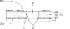
图2A至图2J为本发明的一实施例的一种内埋元件的基板制程的制作流程剖面示意图。首先,请参考图2A,提供一核心层210,核心层210具有一第一介电层212、一第一图案化线路层214及一第二图案化线路层216。第一图案化线路层214与第二图案化线路层216分别位于第一介电层212的一上表面212a与一下表面212b。在本实施例中,提供核心层210的步骤包括利用微影及蚀刻制程分别图案化位于第一介电层212的上表面212a及下表面212b的一第一金属层(未图示,其材质可为铜)与一第二金属层(未图示,其材质可为铜),以在第一介电层212的上表面212a及下表面212b上分别形成第一图案化线路层214与第二图案化线路层216。2A to FIG. 2J are cross-sectional schematic diagrams of a manufacturing process of a substrate manufacturing process for embedded components according to an embodiment of the present invention. First, please refer to FIG. 2A , a
接着,请参考图2B,在核心层210中形成一贯孔H3,而贯孔H3可利用机械钻孔、雷射成孔或其它方式形成。接着,请参考图2C,将核心层210配置于一支撑板S上,且将一内埋元件E’置放于贯孔H3中,其中内埋元件E’具有至少一电极E1’(在图2C中设置有两个电极E1’)。在本实施例中,支撑板S可为一玻璃板、一聚对苯二酸乙烯酯膜或是其它材料所构成的板件;此外,内埋元件E’包括主动元件(例如是薄膜晶体管)及被动元件(例如是电阻、电容或电感)。值得注意的是,因为内埋元件E’与第二图案化线路层216是由支撑板S所支撑,所以内埋元件E’与第二图案化导电层216大约位于支撑板S的同一平面上。Next, please refer to FIG. 2B , a through hole H3 is formed in the
再来,请参考图2D,进行一灌胶制程,使内埋元件E’固定于贯孔H3中。在本实施例中,此灌胶制程是将一黏着剂A填充于内埋元件E’与贯孔H3之间的间隙中,并将其固化,使内埋元件E’固定在核心层210的贯孔H3中。此外,黏着剂A可为热固型树脂(thermal setting resin)或是紫外光固化型树脂,以分别通过加热或以紫外线照射的方式将其固化(curing)。之后,请参考图2E,移除支撑板S。Next, referring to FIG. 2D , a glue filling process is performed to fix the embedded component E' in the through hole H3. In this embodiment, the potting process is to fill an adhesive A into the gap between the embedded element E' and the through hole H3, and then cure it, so that the embedded element E' is fixed on the
接下来,请继续参考图2E,电性连接内埋元件E’的电极E1’与第二图案化线路层216。通过这种方式完成基本的内埋元件的基板制程。Next, please continue to refer to FIG. 2E , to electrically connect the electrode E1' of the embedded element E' and the second
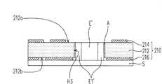
以下将搭配图示说明其中一种电性连接内埋元件E’的电极E1’与第二图案化线路层216的制作方法,然而,使用者也可通过其它方式使内埋元件E’的电极E1’与第二图案化线路层216构成电性连接,本发明对此不作任何限制。图3A至图3C为电性连接内埋元件的电极与第二图案化线路层的制作流程剖面示意图。具体而言,首先,请参考图3A,在第二图案化线路层216上配置一屏蔽M,屏蔽M暴露出电极E1’与部分第二图案化线路层216。接着,请参考图3B,在第一介电层212的下表面212b形成一金属层L,其中部分金属层L是电性连接电极E1’与第二图案化线路层216。形成金属层L的方法包括电镀、无电镀、物理气相沉积法、化学气相沉积法,或者是在第一介电层212的下表面212b涂布一层导电胶也可。再者,请参考图3B与图3C,移除屏蔽M,通过这种方式,内埋元件E’的电极E1’即可透过金属层L与第二图案化线路层216构成电性连接。在此必须说明的是,在上述电性连接内埋元件E’的电极E1’与第二图案化线路层216时,可同时电性连接内埋元件E’的电极E1’与第一图案化线路层214,但是在此并未以图面绘示。One of the fabrication methods for electrically connecting the electrode E1' of the embedded element E' to the second
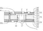
而在完成图2E所绘示的电性连接内埋元件E’的电极E1’与第二图案化线路层216的步骤后,更可利用下列两种方式在基板两侧的表面形成表层线路、焊罩层及抗氧化层,以使基板成为具有双层线路层的基板。After completing the step of electrically connecting the electrode E1' of the embedded element E' and the second
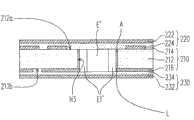
图2F至2J为在基板上预先保留下电镀线,以在基板的表面上依序形成表层线路、焊罩层及抗氧化层的制作流程剖面图。首先,请参考图2F,将一第一叠合层220与一第二叠合层230分别配置于第一图案化线路层214与第二图案化线路层216上。其中第一叠合层220包括一第三金属层222及一第二介电层224,第二叠合层230包括一第四金属层232及一第三介电层234,且第二介电层224与第三介电层234是分别朝向第一图案化线路层214与第二图案化线路层216,换句话来讲,第二介电层224是介于第三金属层222与第一图案化线路层214之间,而第三介电层234是介于第四金属层232与第二图案化线路层216之间。2F to 2J are cross-sectional views of the manufacturing process of pre-reserving plating lines on the substrate to sequentially form surface circuits, solder mask layers and anti-oxidation layers on the surface of the substrate. First, please refer to FIG. 2F , a first build-
接着,请参考图2G,压合第一叠合层220、核心层210与第二叠合层230,以使得第一图案化线路层214与第二图案化线路层216分别嵌入第二介电层224与第三介电层234,并使第三金属层222与第四金属层232分别配置于第二介电层224与第三介电层234上。Next, referring to FIG. 2G , the first build-
再来,请参考图2H,在第一叠合层220、核心层210与第二叠合层230之间形成至少一导电通孔H4,换句话来讲,导电通孔H4贯穿第一叠合层220、核心层210与第二叠合层230。导电通孔H4的形成方式是例如先以机械钻孔或雷射成孔的的方式形成一贯通孔,再在此贯通孔侧壁周围或内部镀上铜金属以形成导电通孔H4。Next, please refer to FIG. 2H, at least one conductive via H4 is formed between the first build-
再者,请参考图2H与图2I,通过例如微影与蚀刻制程来图案化第三金属层222与第四金属层232,以分别形成一第一表层线路222’与一第二表层线路232’,而第一表层线路222’与第二表层线路232’是通过导电通孔H4而电性导通。Furthermore, referring to FIG. 2H and FIG. 2I, the
之后,请参考图2J,在第二介电层224与第三介电层234上分别形成一第一焊罩层240与一第二焊罩层250,其中第一焊罩层240暴露出至少部分第一表层线路222’,而第二焊罩层250暴露出至少部分第二表层线路232’。在此必须说明的是,第一焊罩层240与第二焊罩层250分别用以保护第一表层线路222’与第二表层线路232’,而第一焊罩层240所暴露出的部分第一表层线路222’与第二焊罩层250所暴露出的部分第二表层线路232’例如可以作为电性接垫(electrical pad),其用以作为电性连接外部电子装置或元件的接点。Afterwards, referring to FIG. 2J , a first
接着,在第一焊罩层240所暴露的至少部分第一表层线路222’上形成一第一抗氧化层260,并且在第二焊罩层250所暴露的至少部分第二表层线路232’上形成一第二抗氧化层270。第一抗氧化层260与第二抗氧化层270的材质可为不易氧化的导电材料,例如是镍或金,其可以采用电镀的方式形成,以避免所暴露出的部分第一表层线路222’与第二表层线路232’因接触空气与水气而氧化。Next, a
在本发明另一实施例中,上述以图2J所绘示的形成焊罩层与抗氧化层的步骤可作步骤顺序的改变。请参考图2I与图4,其中图4为本发明另一实施例的形成焊罩层与抗氧化层的制作流程剖面示意图。在形成图2I所示的第一表层线路222’与第二表层线路232’之后,可包括以下步骤。首先,例如以微影与蚀刻的制程在第一表层线路222’与第二表层线路232’上分别形成图案化的一第一抗氧化层260’与图案化的一第二抗氧化层270’。In another embodiment of the present invention, the above-mentioned steps of forming the solder mask layer and the anti-oxidation layer shown in FIG. 2J can be changed in sequence. Please refer to FIG. 2I and FIG. 4 , wherein FIG. 4 is a cross-sectional schematic diagram of a manufacturing process for forming a solder mask layer and an anti-oxidation layer according to another embodiment of the present invention. After forming the first surface circuit 222' and the second surface circuit 232' shown in FIG. 2I, the following steps may be included. Firstly, a patterned
接着,在第二介电层224与第三介电层234上分别形成一第一焊罩层240’与一第二焊罩层250’,其中第一焊罩层240’覆盖第一表层线路222’,并暴露出第一抗氧化层260’,而第二焊罩层250’覆盖第二表层线路232’,并暴露出第二抗氧化层270’。在本实施例中,第一焊罩层240’与第二焊罩层250’的功能如同上述第一焊罩层240与第二焊罩层250(请参考图2J),而第一抗氧化层260’与第二抗氧化层270’的材质、形成方式与功能则如同上述第一抗氧化层260与第二抗氧化层270(请参考图2J),所以在此就不再详细叙述。Next, a first solder mask layer 240' and a second solder mask layer 250' are respectively formed on the
综上所述,本发明的内埋元件的基板制程,至少具有下列优点:In summary, the substrate manufacturing process for embedded components of the present invention has at least the following advantages:
(一)由于在本发明的内埋元件的基板制程中,内埋元件的电极电性连接至内层的第一图案化线路层或第二图案化线路层,因此可以提升第一图案化线路层、第二图案化线路层、第一表层线路与第二表层线路的布线密度,以及改善内埋元件与第一图案化线路层或第二图案化线路层的电性连接的可靠度;(1) Since the electrodes of the embedded components are electrically connected to the first patterned circuit layer or the second patterned circuit layer of the inner layer in the substrate manufacturing process of the embedded components of the present invention, the first patterned circuit layer can be improved. layer, the second patterned circuit layer, the wiring density of the first surface layer circuit and the second surface layer circuit, and improve the reliability of the electrical connection between the embedded element and the first patterned circuit layer or the second patterned circuit layer;
(二)由于内埋元件不需透过现有的导电通孔而直接与内层的第一图案化线路层或第二图案化线路层电性连接,因此可有效地减少整个基板的厚度,使得应用此基板的电子产品可符合轻薄短小的产品设计要求;(2) Since the embedded components are directly electrically connected to the first patterned circuit layer or the second patterned circuit layer of the inner layer without passing through the existing conductive vias, the thickness of the entire substrate can be effectively reduced, The electronic products using this substrate can meet the design requirements of thin, light and small products;
(三)由于在本发明的内埋元件的基板制程中,内埋元件的电极电性连接至内层的第一图案化线路层或第二图案化线路层,因此可以降低内埋元件的电极与第一图案化线路层或第二图案化线路层之间传输电性信号的串音效应(cross-talk effect),进而提升其电性表现(electrical performance);(3) Since the electrodes of the embedded components are electrically connected to the first patterned circuit layer or the second patterned circuit layer of the inner layer in the substrate manufacturing process of the embedded components of the present invention, the electrodes of the embedded components can be reduced. The cross-talk effect (cross-talk effect) of transmitting electrical signals between the first patterned circuit layer or the second patterned circuit layer, thereby improving its electrical performance (electrical performance);
(四)由于在本发明的内埋元件的基板制程中,内埋元件的电极不以形成导电孔道的方式而电性连接至内层的第一图案化线路层或第二图案化线路层,因此本发明的内埋元件的基板制程的制造成本较低。(4) Since in the substrate manufacturing process of the embedded component of the present invention, the electrode of the embedded component is not electrically connected to the first patterned circuit layer or the second patterned circuit layer of the inner layer by forming a conductive hole, Therefore, the manufacturing cost of the embedded element substrate manufacturing process of the present invention is relatively low.
Claims (11)
Translated fromChinesePriority Applications (1)
| Application Number | Priority Date | Filing Date | Title |
|---|---|---|---|
| CN200710100549ACN100584155C (en) | 2007-04-10 | 2007-04-10 | Substrate process for embedded components |
Applications Claiming Priority (1)
| Application Number | Priority Date | Filing Date | Title |
|---|---|---|---|
| CN200710100549ACN100584155C (en) | 2007-04-10 | 2007-04-10 | Substrate process for embedded components |
Publications (2)
| Publication Number | Publication Date |
|---|---|
| CN101287340A CN101287340A (en) | 2008-10-15 |
| CN100584155Ctrue CN100584155C (en) | 2010-01-20 |
Family
ID=40059225
Family Applications (1)
| Application Number | Title | Priority Date | Filing Date |
|---|---|---|---|
| CN200710100549AActiveCN100584155C (en) | 2007-04-10 | 2007-04-10 | Substrate process for embedded components |
Country Status (1)
| Country | Link |
|---|---|
| CN (1) | CN100584155C (en) |
Families Citing this family (2)
| Publication number | Priority date | Publication date | Assignee | Title |
|---|---|---|---|---|
| US9406658B2 (en)* | 2010-12-17 | 2016-08-02 | Advanced Semiconductor Engineering, Inc. | Embedded component device and manufacturing methods thereof |
| CN106376170A (en)* | 2015-07-24 | 2017-02-01 | 宏启胜精密电子(秦皇岛)有限公司 | Flexible circuit board, manufacturing method thereof, and electronic device |
Citations (2)
| Publication number | Priority date | Publication date | Assignee | Title |
|---|---|---|---|---|
| US20040226743A1 (en)* | 2003-03-25 | 2004-11-18 | Advanced Semiconductor Engineering, Inc. | Bumpless assembly package |
| CN1823555A (en)* | 2003-07-24 | 2006-08-23 | 摩托罗拉公司 | Circuit board with embedded components and method of manufacture |
- 2007
- 2007-04-10CNCN200710100549Apatent/CN100584155C/enactiveActive
Patent Citations (2)
| Publication number | Priority date | Publication date | Assignee | Title |
|---|---|---|---|---|
| US20040226743A1 (en)* | 2003-03-25 | 2004-11-18 | Advanced Semiconductor Engineering, Inc. | Bumpless assembly package |
| CN1823555A (en)* | 2003-07-24 | 2006-08-23 | 摩托罗拉公司 | Circuit board with embedded components and method of manufacture |
Also Published As
| Publication number | Publication date |
|---|---|
| CN101287340A (en) | 2008-10-15 |
Similar Documents
| Publication | Publication Date | Title |
|---|---|---|
| US7550320B2 (en) | Method of fabricating substrate with embedded component therein | |
| TWI466607B (en) | Printed circuit board having buried component and method for manufacturing same | |
| CN103260356B (en) | Flying tail type rigid-flexible printed circuit board and manufacturing method thereof | |
| JP2017143254A (en) | Wiring board having lamination and embedded capacitor and manufacturing method | |
| CN108987371A (en) | Element embedded type packaging carrier plate and manufacturing method thereof | |
| US7338892B2 (en) | Circuit carrier and manufacturing process thereof | |
| JP6614246B2 (en) | Capacitor built-in multilayer wiring board and manufacturing method thereof | |
| KR101155624B1 (en) | Embedded pcb and manufacturing method for the same | |
| CN101436549A (en) | Method for manufacturing copper core layer multilayer packaging substrate | |
| CN104756615B (en) | Printed circuit board | |
| TW201427509A (en) | Printed circuit board having buried component and method for manufacturing same | |
| TW201424501A (en) | Package structure and method for manufacturing same | |
| CN101038885A (en) | Substrate Manufacturing Method for Embedded Components | |
| CN101038886A (en) | Substrate Manufacturing Method for Embedded Components | |
| US7728234B2 (en) | Coreless thin substrate with embedded circuits in dielectric layers and method for manufacturing the same | |
| CN101677067B (en) | Manufacturing method of copper core layer multilayer packaging substrate | |
| CN103974521A (en) | Multilayer wiring board and method for manufacturing same | |
| CN100584155C (en) | Substrate process for embedded components | |
| CN106341945A (en) | Flexible circuit board and manufacturing method thereof | |
| CN100459078C (en) | Method for manufacturing substrate | |
| CN101594752A (en) | How to make a multilayer circuit board | |
| KR101580472B1 (en) | Method for manufacturing a circuit board | |
| JP6637608B2 (en) | Component-embedded substrate and manufacturing method thereof | |
| CN101677068A (en) | Method for manufacturing copper core layer multilayer packaging substrate | |
| TW201427505A (en) | Printed circuit board having buried component and method for manufacturing same |
Legal Events
| Date | Code | Title | Description |
|---|---|---|---|
| C06 | Publication | ||
| PB01 | Publication | ||
| C10 | Entry into substantive examination | ||
| SE01 | Entry into force of request for substantive examination | ||
| C14 | Grant of patent or utility model | ||
| GR01 | Patent grant |