CN100576893C - A graphic OSD controller integrated in video processing chip - Google Patents
A graphic OSD controller integrated in video processing chipDownload PDFInfo
- Publication number
- CN100576893C CN100576893CCN200710018552ACN200710018552ACN100576893CCN 100576893 CCN100576893 CCN 100576893CCN 200710018552 ACN200710018552 ACN 200710018552ACN 200710018552 ACN200710018552 ACN 200710018552ACN 100576893 CCN100576893 CCN 100576893C
- Authority
- CN
- China
- Prior art keywords
- osd
- module
- image
- data
- display
- Prior art date
- Legal status (The legal status is an assumption and is not a legal conclusion. Google has not performed a legal analysis and makes no representation as to the accuracy of the status listed.)
- Expired - Fee Related
Links
- 238000012545processingMethods0.000titleclaimsabstractdescription24
- 238000003860storageMethods0.000claimsabstractdescription50
- 238000013507mappingMethods0.000claimsabstractdescription30
- 230000006837decompressionEffects0.000claimsabstractdescription5
- 230000001133accelerationEffects0.000claimsdescription27
- 230000015654memoryEffects0.000claimsdescription24
- 238000004364calculation methodMethods0.000claimsdescription23
- 238000013500data storageMethods0.000claimsdescription17
- 238000007726management methodMethods0.000claimsdescription17
- 238000000034methodMethods0.000claimsdescription11
- 230000006870functionEffects0.000claimsdescription8
- 230000007274generation of a signal involved in cell-cell signalingEffects0.000claimsdescription7
- 239000000463materialSubstances0.000claimsdescription5
- 238000007906compressionMethods0.000claimsdescription4
- 230000006835compressionEffects0.000claimsdescription4
- 238000006243chemical reactionMethods0.000claimsdescription3
- 238000013144data compressionMethods0.000claimsdescription3
- 230000010354integrationEffects0.000abstractdescription3
- 238000013461designMethods0.000description17
- 238000010586diagramMethods0.000description11
- 238000005516engineering processMethods0.000description6
- 230000015572biosynthetic processEffects0.000description5
- 238000003786synthesis reactionMethods0.000description5
- 238000001514detection methodMethods0.000description3
- 230000000694effectsEffects0.000description2
- 230000004044responseEffects0.000description2
- 238000012546transferMethods0.000description2
- 230000000903blocking effectEffects0.000description1
- 239000003086colorantSubstances0.000description1
- 238000004891communicationMethods0.000description1
- 239000002131composite materialSubstances0.000description1
- 230000001934delayEffects0.000description1
- 238000011161developmentMethods0.000description1
- 238000009826distributionMethods0.000description1
- 230000006872improvementEffects0.000description1
- 238000004519manufacturing processMethods0.000description1
- 230000008569processEffects0.000description1
- 238000011160researchMethods0.000description1
- 230000003068static effectEffects0.000description1
- 230000001360synchronised effectEffects0.000description1
- 230000007704transitionEffects0.000description1
Images


Landscapes
- Controls And Circuits For Display Device (AREA)
Abstract
Translated fromChineseDescription
Translated fromChinese技术领域technical field
本发明属于数字视频图像处理与显示技术领域,具体涉及一种集成于视频处理芯片的图形OSD控制器。The invention belongs to the technical field of digital video image processing and display, and in particular relates to a graphics OSD controller integrated in a video processing chip.
背景技术Background technique
OSD控制器是视频显示处理系统中不可或缺的部分,它能够提供多种语言界面使用户可以通过各项功能菜单来调节所有视频显示图像的特性。早期的OSD系统主要是字符单元显示为主,其特点是颜色单一,大小固定,菜单设计的图案也比较简单。随着数字视频处理技术的飞速发展,各类先进复杂的算法应用于视频处理芯片向消费者提供了更加清晰流畅的视频图像,同时人们对OSD菜单的要求也越来越高。以位图方式显示的OSD控制器已成为视频处理系统的主流,特别是随着IC设计和生产的水平不断提高,OSD控制器更向集成化方向发展。The OSD controller is an indispensable part of the video display processing system. It can provide multiple language interfaces so that users can adjust the characteristics of all video display images through various function menus. The early OSD system was mainly based on the display of character units, which was characterized by a single color, fixed size, and relatively simple menu design patterns. With the rapid development of digital video processing technology, various advanced and complex algorithms are applied to video processing chips to provide consumers with clearer and smoother video images. At the same time, people have higher and higher requirements for OSD menus. OSD controllers displayed in bitmaps have become the mainstream of video processing systems, especially with the continuous improvement of IC design and production, OSD controllers are developing towards integration.
图形OSD控制器是指在视频显示画面中可以显示单色或彩色位图,因此菜单的形式更加多样,画面更加精美,内容也更加丰富。同时,由于图形OSD控制器设计的复杂度不断提高,OSD控制器也将占用更大的存储空间和系统资源。因此如何将图形OSD控制器和视频处理器有效的集成,并合理的共享存储资源以及总线带宽成为各大厂商的研究热点。Graphic OSD controller means that monochrome or color bitmap can be displayed in the video display screen, so the menu forms are more diverse, the picture is more exquisite, and the content is more abundant. At the same time, since the design complexity of the graphic OSD controller continues to increase, the OSD controller will also occupy a larger storage space and system resources. Therefore, how to effectively integrate the graphics OSD controller and video processor, and reasonably share storage resources and bus bandwidth has become a research hotspot for major manufacturers.
发明内容Contents of the invention
本发明的目的在于,提供一种集成于视频处理芯片的高性能图形OSD控制器的设计方法。该图形OSD控制器采用现代先进的集成电路设计技术,通过共享视频处理系统的外部动态存储器和内部静态存储器资源,实现了具有256种伪彩色的图形OSD显示功能,且该图形OSD控制器具有方便的用户软件编程接口。The object of the present invention is to provide a design method of a high-performance graphics OSD controller integrated in a video processing chip. The graphic OSD controller adopts modern advanced integrated circuit design technology, and realizes the graphic OSD display function with 256 kinds of false colors by sharing the external dynamic memory and internal static memory resources of the video processing system, and the graphic OSD controller has a convenient user software programming interface.
为了实现上述任务,本发明采取如下的解决技术方案:In order to achieve the above tasks, the present invention takes the following technical solutions:
一种集成于视频处理芯片的图形OSD控制器,其特征在于,该图形OSD控制器的内部结构包括:A kind of graphics OSD controller integrated in video processing chip, it is characterized in that, the internal structure of this graphics OSD controller comprises:
一位图数据解压缩模块,用于将压缩编码后OSD数据解压缩为位图索引数据,数据压缩采用改进的游程编码算法,压缩部分由软件实现;A bitmap data decompression module is used to decompress compressed and coded OSD data into bitmap index data. The data compression adopts an improved run-length coding algorithm, and the compression part is realized by software;
一存储操作控制模块,利用片外SDRAM存储器和片内双端口RAM资源,实现OSD图像数据的写入、存储、生成和显示加速功能;A storage operation control module, which uses off-chip SDRAM memory and on-chip dual-port RAM resources to realize the writing, storage, generation and display acceleration functions of OSD image data;
一可编程色彩映射模块,利用片内存储的色彩映射表(OSD_LUT)将输入的原始图像索引数据流映射为RGB空间24位伪彩色数据流,实现图像索引值到彩色空间的映射转换;A programmable color mapping module, using the color mapping table (OSD_LUT) stored in the chip to map the input original image index data stream into a 24-bit pseudo-color data stream in RGB space, and realize the mapping conversion from the image index value to the color space;
一OSD图像缩放模块,利用双线性图像插值的方法,在水平和垂直两个方向上灵活调整已生成的OSD图像的大小,以适应不同格式的视频信号或不同分辨率的显示终端;An OSD image scaling module, which uses a bilinear image interpolation method to flexibly adjust the size of the generated OSD image in the horizontal and vertical directions, so as to adapt to video signals in different formats or display terminals with different resolutions;
一OSD图像显示管理模块,根据OSD控制器的参数设置,控制多层OSD数据的叠加方式、OSD图像与原始视频信号的混合模式、OSD图像显示窗口大小等显示特性;An OSD image display management module, according to the parameter settings of the OSD controller, controls the display characteristics such as the superposition mode of multi-layer OSD data, the mixing mode of OSD image and original video signal, and the size of the OSD image display window;
一寄存器操作管理模块,由用户操作设置其它模块的各项参数,并控制OSD原始图像素材的写入、存储控制以及显示特性;A register operation management module, which is operated by the user to set various parameters of other modules, and controls the writing, storage control and display characteristics of OSD original image materials;
一MCU接口模块,提供串行和并行两种工作模式,设置寄存器操作管理模块的各种显示参数、操作参数,从而控制OSD数据的存储、显示并读取OSD控制器的状态;An MCU interface module, providing serial and parallel working modes, setting various display parameters and operating parameters of the register operation management module, thereby controlling the storage and display of OSD data and reading the status of the OSD controller;
在寄存器操作管理模块的控制下,解压缩后的OSD索引数据流经存储操作控制模块写入外部SDRAM的OSD数据存储区,并在该模块的控制下完成从OSD数据存储区到OSD显示缓存区的搬运。OSD图像显示时,由存储操作控制模块控制读出OSD显示缓存区的索引数据,经可编程色彩映射模块转换成RGB空间24位图像数据流,OSD图像数据通过图像缩放模块灵活调整图像的分辨率,最终在OSD图像显示管理模块产生的有效信号(OSD_ACTIVE)控制下与原始视频信号叠加。Under the control of the register operation management module, the decompressed OSD index data flows through the storage operation control module and is written into the OSD data storage area of the external SDRAM, and is completed from the OSD data storage area to the OSD display buffer area under the control of the module handling. When the OSD image is displayed, the index data of the OSD display buffer area is controlled by the storage operation control module to read out, and converted into a 24-bit image data stream in RGB space through the programmable color mapping module, and the OSD image data is flexibly adjusted to the resolution of the image through the image scaling module , and finally superimposed with the original video signal under the control of the effective signal (OSD_ACTIVE) generated by the OSD image display management module.
本发明的其它特点是所述的存储操作控制模块包括有仲裁器、地址产生模块、命令产生模块、输入缓存模块、输出缓存模块和加速缓存模块,地址产生模块、命令产生模块与仲裁器连接,输入缓存模块通过写请求与仲裁器连接,输出缓存模块通过读请求与仲裁器连接,加速缓存模块通过加速请求与仲裁器相连。Other features of the present invention are that the storage operation control module includes an arbiter, an address generation module, a command generation module, an input cache module, an output cache module, and an acceleration cache module, and the address generation module and the command generation module are connected to the arbiter, The input cache module is connected to the arbitrator through a write request, the output cache module is connected to the arbitrator through a read request, and the acceleration cache module is connected to the arbitrator through an acceleration request.
所述的OSD图像缩放模块包括数据存储器、插值计算模块、写入控制模块,读出控制模块,控制信号产生模块,映射参数计算模块;控制信号产生模块分别与写入控制模块、读出控制模块、映射参数计算模块连通,写入控制模块、读出控制模块与数据存储器相连,数据存储器与插值计算模块相连,映射参数计算模块分别与读出控制模块、插值计算模块连接。Described OSD image scaling module comprises data memory, interpolation calculation module, writing control module, readout control module, control signal generation module, mapping parameter calculation module; Control signal generation module and write control module, readout control module respectively The mapping parameter calculation module is connected, the writing control module and the reading control module are connected to the data storage, the data storage is connected to the interpolation calculation module, and the mapping parameter calculation module is respectively connected to the reading control module and the interpolation calculation module.
所述的外SDRAM存储器划分为OSD数据存储区和OSD显示缓存区,通过存储操作控制模块控制片外SDRAM存储器和片内双端口RAM资源,实现OSD图像数据的写入、存储、生成和显示加速功能。The external SDRAM memory is divided into an OSD data storage area and an OSD display buffer area, and the external SDRAM memory and the on-chip dual-port RAM resource are controlled by the storage operation control module to realize the writing, storage, generation and display acceleration of OSD image data Function.
所述的仲裁模块对读写请求和显示加速请求信号进行仲裁,产生相应的控制信号以完成多任务调度。The arbitration module arbitrates the read-write request and the display acceleration request signal, and generates corresponding control signals to complete multi-task scheduling.
OSD图像缩放模块利用双线性插值的方法对图像进行缩放,在水平和垂直两个方向上灵活调整已生成的OSD图像的大小,以适应不同格式的视频信号或不同分辨率的显示终端。The OSD image scaling module uses the method of bilinear interpolation to scale the image, and flexibly adjusts the size of the generated OSD image in the horizontal and vertical directions to adapt to video signals of different formats or display terminals of different resolutions.
本发明的集成于视频处理芯片的图形OSD控制器,将图形OSD控制器采用当前先进的集成电路设计方法实现,可以方便的与视频处理器芯片集成。The graphics OSD controller integrated in the video processing chip of the present invention is realized by adopting the current advanced integrated circuit design method, and can be conveniently integrated with the video processor chip.
与已有技术相比,本发明的技术效果体现在:Compared with prior art, technical effect of the present invention is reflected in:
1.本发明支持位图数据的压缩编码,有效地降低了OSD图像数据对外部存储空间的需求,有利于复杂的OSD图形菜单设计;1. The present invention supports the compression coding of bitmap data, which effectively reduces the requirement of external storage space for OSD image data, and is conducive to the design of complex OSD graphic menus;
2.本发明对字符、文字和图形全部采用按点象素的位图合成方式,结构设计简单,编程接口统一方便;2. The present invention all adopts the bitmap synthesis mode by dot pixel to character, literal and figure, and structural design is simple, and programming interface is unified and convenient;
3.本发明存储器资源的分配,使用片外SDRAM作为图像数据的显示存储,使用片内双端口RAM作为图像操作的控制存储,便于与视频处理系统集成和共享资源;3. The distribution of memory resources of the present invention uses off-chip SDRAM as the display storage of image data, and uses on-chip dual-port RAM as the control storage of image operation, which is convenient for integrating and sharing resources with the video processing system;
4.本发明对OSD图像显示支持硬件加速操作,可将OSD数据存储区的图形高速块拷贝到OSD显示缓存区,并支持图像块的快速搬移、图像块的快速色彩填充等硬件加速操作,可有效提高OSD菜单的响应速度,提高编程效率并节省存储资源;4. The present invention supports hardware acceleration operation for OSD image display, can copy the graphic high-speed blocks of the OSD data storage area to the OSD display buffer area, and supports hardware acceleration operations such as fast moving of image blocks, fast color filling of image blocks, etc. Effectively improve the response speed of the OSD menu, improve programming efficiency and save storage resources;
5.本发明生成的OSD图像可根据视频显示格式和显示终端的分辨率灵活地调整图像大小,显示方式更加灵活;5. The OSD image generated by the present invention can flexibly adjust the image size according to the video display format and the resolution of the display terminal, and the display mode is more flexible;
6.本发明设计的OSD控制器具有串行I2C和并行两种MCU操作接口,对控制器内部的寄存器操作方式更加灵活,优于接口单一的控制器;6. The OSD controller designed by the present invention has two kinds of MCU operation interfaces, serial I2C and parallel, and is more flexible to the register operation mode inside the controller, and is better than a single controller with an interface;
7.在实际性能方面,本发明在一款采用TSMC 0.18um混合信号集成电路工艺的视频处理芯片的应用实例中,完成了图形OSD菜单设计的各项要求。本发明设计的OSD控制器与视频处理芯片共享系统总线带宽,支持包括HDTV 1080I(数据时钟高达74.25MHz)在内的多种视频格式的图形菜单显示。本发明设计的OSD控制器逻辑综合后,逻辑资源仅3万余门,优于一般设计的OSD控制器。7. In terms of actual performance, the present invention has completed the requirements of graphic OSD menu design in an application example of a video processing chip using TSMC 0.18um mixed-signal integrated circuit technology. The OSD controller designed by the present invention shares the system bus bandwidth with the video processing chip, and supports graphic menu display in multiple video formats including HDTV 1080I (data clock up to 74.25MHz). After the logic synthesis of the OSD controller designed by the present invention, the logic resource is only more than 30,000 gates, which is better than the OSD controller of general design.
附图说明Description of drawings
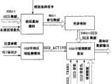
图1为本发明的OSD控制器的内部结构框图;Fig. 1 is the internal structural block diagram of OSD controller of the present invention;
图2为OSD存储资源的分配图;FIG. 2 is an allocation diagram of OSD storage resources;
图3为存储操作控制模块功能框图;Fig. 3 is a functional block diagram of the storage operation control module;
图4为存储任务调度状态机;Fig. 4 is storage task scheduling state machine;
图5为双线性插值在一维方向上各象素点位置关系的示意图;Fig. 5 is the schematic diagram of the positional relationship of each pixel point in the one-dimensional direction for bilinear interpolation;
图6为OSD图像缩放模块功能框图;Fig. 6 is a functional block diagram of the OSD image scaling module;
图7为OSD图像合成原理图;Fig. 7 is a schematic diagram of OSD image synthesis;
图8为I2C总线控制器状态机。Figure 8 is the I2C bus controller state machine.
以下结合附图和实施例对本发明作进一步的详细说明。The present invention will be further described in detail below in conjunction with the accompanying drawings and embodiments.
具体实施方式Detailed ways
参见图1,本发明的集成于视频处理芯片的图形OSD控制器,其内部基本结构包括位图数据解压缩模块、存储操作控制模块、可编程色彩映射模块、OSD图像缩放模块、OSD图像显示管理模块、寄存器操作管理模块和MCU接口模块;用户通过MCU接口设置寄存器操作控制模块的各寄存器和控制参数输出,从而完成存储操作、色彩映射和显示合成等多种功能。Referring to Fig. 1, the graphic OSD controller integrated in video processing chip of the present invention, its internal basic structure comprises bitmap data decompression module, storage operation control module, programmable color mapping module, OSD image scaling module, OSD image display management Module, register operation management module and MCU interface module; the user sets the registers and control parameter output of the register operation control module through the MCU interface, so as to complete various functions such as storage operation, color mapping and display synthesis.
位图数据经压缩后,可以有效地降低对片外位图数据的存储空间需求。位图数据解压缩模块用于将OSD数据解压缩为位图索引数据,数据压缩采用改进的游程编码(BLE)算法,压缩部分由软件实现。After the bitmap data is compressed, the storage space requirement for off-chip bitmap data can be effectively reduced. The bitmap data decompression module is used to decompress OSD data into bitmap index data. The data compression adopts the improved run-length encoding (BLE) algorithm, and the compression part is realized by software.
存储操作控制模块,利用片外SDRAM存储器和片内双端口RAM资源,实现OSD图像数据的写入、存储、生成和显示加速等功能。The storage operation control module uses off-chip SDRAM memory and on-chip dual-port RAM resources to realize functions such as writing, storing, generating and displaying acceleration of OSD image data.
可编程色彩映射模块,利用片内存储的色彩映射表(OSD_LUT)将输入的原始图像索引数据流映射为RGB空间24位伪彩色数据流,实现图像索引值到彩色空间的映射转换。The programmable color mapping module uses the color mapping table (OSD_LUT) stored on-chip to map the input original image index data stream into a 24-bit pseudo-color data stream in RGB space, realizing the mapping conversion from image index value to color space.
OSD图像缩放模块,利用双线性图像插值的方法,可在水平和垂直两个方向上灵活调整已生成的OSD图像的大小,以适应不同格式的视频信号或不同分辨率的显示终端。The OSD image scaling module uses the method of bilinear image interpolation to flexibly adjust the size of the generated OSD image in the horizontal and vertical directions to adapt to video signals of different formats or display terminals of different resolutions.
OSD图像显示管理模块,可根据OSD控制器的参数设置,控制多层图形OSD数据的叠加方式、OSD图像与原始视频信号的混合模式、OSD图像显示窗口大小以及显示特性等。The OSD image display management module can control the overlay mode of multi-layer graphics OSD data, the mixing mode of OSD image and original video signal, the size of the OSD image display window and display characteristics according to the parameter settings of the OSD controller.
寄存器操作管理模块,可由用户操作设置其它模块的各项参数,并控制OSD原始图像素材的写入、存储控制以及显示特性等各种模式。The register operation management module can be operated by the user to set various parameters of other modules, and control various modes such as writing of OSD original image materials, storage control, and display characteristics.
MCU接口模块,提供的串行和并行两种工作模式,用于设置寄存器操作管理模块的各种显示参数和操作参数,从而控制OSD数据的存储、显示并读取OSD控制器的状态。The MCU interface module provides serial and parallel working modes, which are used to set various display parameters and operating parameters of the register operation management module, so as to control the storage and display of OSD data and read the status of the OSD controller.
在寄存器操作管理模块的控制下,解压缩后的OSD索引数据流经存储操作控制模块控制写入OSD数据存储区,并在该模块的控制下完成从数据存储区到显示缓存区的搬运。图像显示时,由存储操作控制模块读出OSD显示缓存区的索引数据,经可编程色彩映射模块转换成RGB空间24位图像数据流。图像数据可通过OSD图像缩放模块灵活调整图像的分辨率,并最终在OSD图像显示管理模块产生的有效信号(OSD_ACTIVE)控制下与原始视频信号叠加。Under the control of the register operation management module, the decompressed OSD index data is written into the OSD data storage area under the control of the storage operation control module, and the transfer from the data storage area to the display buffer area is completed under the control of the module. When the image is displayed, the index data of the OSD display buffer area is read out by the storage operation control module, and converted into a 24-bit image data stream in RGB space by the programmable color mapping module. The image data can flexibly adjust the resolution of the image through the OSD image scaling module, and finally superimpose with the original video signal under the control of the effective signal (OSD_ACTIVE) generated by the OSD image display management module.
如图2所示,本发明设计中使用的存储资源包括片外SDRAM存储器和片内双端口RAM存储器。片外SDRAM存储器划分为OSD数据存储区和OSD显示缓存区;通过存储操作控制模块控制片外SDRAM存储器和片内双端口RAM资源,实现OSD图像数据的写入、存储、生成和显示加速功能。As shown in Figure 2, the storage resources used in the design of the present invention include off-chip SDRAM memory and on-chip dual-port RAM memory. The off-chip SDRAM memory is divided into OSD data storage area and OSD display buffer area; the off-chip SDRAM memory and on-chip dual-port RAM resources are controlled by the storage operation control module to realize the writing, storage, generation and display acceleration functions of OSD image data.
片外SDRAM存储器一般被视频处理芯片作为帧存,而本发明共享SDRAM的空间来存储OSD图形菜单数据。共享的SDRAM空间划分为OSD数据存储区和OSD显示缓存区两部分。其中,OSD数据存储区存储OSD图形设计的位图素材,OSD显示缓存区存储将要显示的OSD图形界面。输入缓存(INPUT_BUFFER)、输出缓存(OUTPUT_BUFFER)、加速缓存(VAC_BUFFER)均为双端口存储器,在存储控制模块的配合下实现对SDRAM的读写操作。OSD_LUT是由一个256x24bits双端口RAM构成的一个地址映射表,将8位的图像索引数据映射到RGB空间的24位数据。SCALE_BUFFER是一个2048x24bits双端口RAM构成的存储阵列,为OSD图像缩放模块提供行存储。The off-chip SDRAM memory is generally used as a frame memory by the video processing chip, and the present invention shares the space of the SDRAM to store the OSD graphic menu data. The shared SDRAM space is divided into two parts: OSD data storage area and OSD display buffer area. Wherein, the OSD data storage area stores the bitmap material of the OSD graphic design, and the OSD display buffer area stores the OSD graphic interface to be displayed. The input buffer (INPUT_BUFFER), the output buffer (OUTPUT_BUFFER), and the acceleration buffer (VAC_BUFFER) are dual-port memories, and the read and write operations to SDRAM are realized with the cooperation of the storage control module. OSD_LUT is an address mapping table composed of a 256x24bits dual-port RAM, which maps 8-bit image index data to 24-bit data in RGB space. SCALE_BUFFER is a storage array composed of 2048x24bits dual-port RAM, which provides row storage for the OSD image scaling module.
可见,本发明的关键在于存储操作控制模块的设计,该模块需要能灵活的对SDRAM进行读写操作,并尽可能提高总线带宽的利用率以便于集成。本发明设计的存储操作控制模块结构框图如图3所示。It can be seen that the key of the present invention lies in the design of the storage operation control module, which needs to be able to flexibly perform read and write operations on the SDRAM, and improve the utilization rate of the bus bandwidth as much as possible to facilitate integration. The structural block diagram of the storage operation control module designed by the present invention is shown in FIG. 3 .
仲裁模块对读写请求和显示加速请求信号进行仲裁,产生相应的控制信号以完成多任务调度。The arbitration module arbitrates the read and write requests and display acceleration request signals, and generates corresponding control signals to complete multi-task scheduling.
写请求模块通过检测输入缓存(INPUT_BUFFER)的堆栈深度产生写请求信号,同理,读请求模块、显示加速请求模块分别通过检测输出缓存(OUTPUT_BUFFER)、加速缓存(VAC_BUFFER)的堆栈深度产生读请求和加速读写请求信号。仲裁器(Arbitrator)对读写请求和显示加速请求信号等进行仲裁,产生相应的允许信号,并激励地址产生和命令产生模块生成SDRAM的地址信号和读写控制命令。存储控制单元的设计充分考虑了如何提高带宽利用率,结合SDRAM的特性,主要采取了以下三种技术:The write request module generates a write request signal by detecting the stack depth of the input buffer (INPUT_BUFFER). Similarly, the read request module and the display acceleration request module generate read requests and Speed up read and write request signals. The arbitrator (Arbitrator) arbitrates read and write requests and display acceleration request signals, etc., generates corresponding permission signals, and stimulates the address generation and command generation modules to generate SDRAM address signals and read and write control commands. The design of the storage control unit fully considers how to improve bandwidth utilization, and combines the characteristics of SDRAM, mainly adopts the following three technologies:
(1)利用SDRAM的Burst存取模式,使数据可多字节连续读写;(1) Using the Burst access mode of SDRAM, the data can be read and written continuously in multiple bytes;
(2)利用地址映射的方法尽量读写SDRAM的同一行单元,减少读写操作中的行地址产生;(2) Use the method of address mapping to read and write the same row unit of SDRAM as far as possible, so as to reduce the generation of row addresses in the read and write operations;
(3)利用SDRAM的多Bank结构,隐藏行操作和预充电所需的操作周期。(3) Utilize the multi-Bank structure of SDRAM to hide the operation cycle required for row operation and pre-charging.
存储操作控制模块包括有仲裁器、地址产生模块、命令产生模块、输入缓存模块、输出缓存模块和加速缓存模块,地址产生模块、命令产生模块与仲裁器连接,输入缓存模块通过写请求与仲裁器连接,输出缓存模块通过读请求与仲裁器连接,加速缓存模块通过加速请求与仲裁器相连。The storage operation control module includes an arbiter, an address generation module, a command generation module, an input cache module, an output cache module, and an acceleration cache module. The address generation module and the command generation module are connected to the arbiter, and the input cache module communicates with the arbiter through a write request. connection, the output cache module is connected to the arbitrator through a read request, and the acceleration cache module is connected to the arbitrator through an acceleration request.
存储操作控制模块设计中集成了OSD显示加速技术。当前OSD菜单的设计越来越复杂,界面切换中需要读写大量的位图数据,易造成画面显示的延迟。显示加速技术,可将存储于OSD数据存储区的位图数据无中间干预的块拷贝到OSD显示缓存区,并可完成OSD数据块在显示缓存区(DisplayBuffer)的拷贝(copy)、搬移以及块填充等操作,可提高OSD菜单的响应时间,并有效节省OSD存储资源,提高OSD的编程效率。The OSD display acceleration technology is integrated in the design of the storage operation control module. The design of the current OSD menu is becoming more and more complicated, and a large amount of bitmap data needs to be read and written in the interface switching, which may easily cause delays in the display of the screen. Display acceleration technology, which can copy the bitmap data stored in the OSD data storage area to the OSD display buffer without intermediate intervention, and can complete the copy (copy), move and block of the OSD data block in the display buffer (DisplayBuffer). Filling and other operations can improve the response time of the OSD menu, effectively save OSD storage resources, and improve the programming efficiency of the OSD.
OSD存储任务调度的状态图如图4所示。若“写请求”WR_REQ有效,总线控制权交给“写”;若“读请求”RD_REQ有效,总线控制权交给“读”;若“加速请求”VAC_REQ有效,总线控制权交给“加速”。若两种请求信号同时有效,仲裁器Arbitrator根据各自堆栈深度信息进行仲裁,并保证每种操作都不产生数据遗漏。The state diagram of OSD storage task scheduling is shown in Figure 4. If the "write request" WR_REQ is valid, the bus control right is given to "write"; if the "read request" RD_REQ is valid, the bus control right is given to "reader"; if the "acceleration request" VAC_REQ is valid, the bus control right is given to "acceleration" . If the two request signals are valid at the same time, the arbitrator Arbitrator will perform arbitration according to the respective stack depth information, and ensure that each operation does not generate data omission.
OSD控制器与视频处理芯片集成时,则可利用芯片中的SDRAM控制模块,并加入OSD读写与显示加速的任务调度。When the OSD controller is integrated with the video processing chip, the SDRAM control module in the chip can be used, and the task scheduling of OSD reading and writing and display acceleration can be added.
OSD图像缩放模块可采用双线性插值(Bilinear)的方法对相同的OSD图形素材在水平和垂直两个方向上进行缩放,以支持不同的视频格式和多种分辨率的显示终端。双线性插值是根据周围4个图像点计算待插值点象素值的线性计算方法。以一维空间的计算为例,图5为双线性插值各象素点之间的关系示意图。其中原始图像点用A[i,j]表示,待插值点用B[i,j]表示。待插值点象素值用下式计算:The OSD image scaling module can use bilinear interpolation (Bilinear) method to scale the same OSD graphic material in both horizontal and vertical directions, so as to support different video formats and display terminals with multiple resolutions. Bilinear interpolation is a linear calculation method that calculates the pixel value of the point to be interpolated based on the surrounding 4 image points. Taking the calculation of one-dimensional space as an example, FIG. 5 is a schematic diagram of the relationship between the pixels of the bilinear interpolation. The original image point is represented by A[i, j], and the point to be interpolated is represented by B[i, j]. The pixel value of the point to be interpolated is calculated by the following formula:
B[i,j]=(1-d)*A[i,j]+d*A[i+1,j]B[i,j]=(1-d)*A[i,j]+d*A[i+1,j]
OSD图像缩放模块的功能框图如图6所示,该模块由数据存储器、控制信号产生、写入控制、读出控制、映射参数计算和插值计算等六个单元组成。利用双线性插值的方法对图像进行缩放,在水平和垂直两个方向上灵活调整已生成的OSD图像的大小,以适应不同格式的视频信号或不同分辨率的显示终端。OSD图像缩放模块包括数据存储器、插值计算模块、写入控制模块,读出控制模块,控制信号产生模块,映射参数计算模块;控制信号产生模块分别与写入控制模块、读出控制模块、映射参数计算模块连通,写入控制模块、读出控制模块与数据存储器相连,数据存储器与插值计算模块相连,映射参数计算模块分别与读出控制模块、插值计算模块连接。The functional block diagram of the OSD image scaling module is shown in Figure 6. This module is composed of six units including data memory, control signal generation, write control, read control, mapping parameter calculation and interpolation calculation. The bilinear interpolation method is used to scale the image, and the size of the generated OSD image is flexibly adjusted in the horizontal and vertical directions to adapt to video signals of different formats or display terminals of different resolutions. The OSD image scaling module includes a data memory, an interpolation calculation module, a write control module, a read control module, a control signal generation module, and a mapping parameter calculation module; the control signal generation module is respectively connected with the write control module, the read control module, and the mapping parameter The computing module is connected, the writing control module and the reading control module are connected with the data storage, the data storage is connected with the interpolation calculation module, and the mapping parameter calculation module is respectively connected with the readout control module and the interpolation calculation module.
该模块由控制信号产生单元生成写控制信号控制写入模块产生写数据存储器的地址。OSD图像数据在写信号和地址的控制下写入数据存储器缓存。映射参数计算模块根据控制信号和缩放比例因子,计算产生读出索引i和距离参数d。读出控制单元根据控制信号和索引参数i产生读地址,从数据存储器中读出插值参考点的象素值A[i,j]和A[i+1,j]。插值计算单元根据插值参考点象素值和距离参数d计算得出插值点象素值。OSD图像缩放模块可支持以1/64为步进对原OSD图像进行1/2~2倍缩放,以支持不同的显示终端。In this module, the control signal generating unit generates a writing control signal to control the writing module to generate an address for writing the data memory. The OSD image data is written into the data memory cache under the control of the write signal and address. The mapping parameter calculation module calculates and generates the readout index i and the distance parameter d according to the control signal and the scaling factor. The read control unit generates a read address according to the control signal and the index parameter i, and reads the pixel values A[i, j] and A[i+1, j] of the interpolation reference point from the data memory. The interpolation calculation unit calculates and obtains the pixel value of the interpolation point according to the pixel value of the interpolation reference point and the distance parameter d. The OSD image scaling module can support 1/2-2 times scaling of the original OSD image in steps of 1/64 to support different display terminals.
OSD控制器最多可支持4个OSD图层的合成显示。在色彩映射之前,解压缩后的各图层数据以8位位图索引表征。OSD图像合成原理如图7所示。在图层选择信号及背景色寄存器的控制下,OSD的各图层间以遮挡的方式叠加,叠加后的8位OSD位图索引经色彩映射后转换为24位RGB象素数据。另外,OSD窗口检测模块根据OSD的位置参数(包括窗口的起始点坐标OSD_SX、OSD_SY及窗口水平、垂直方向的大小OSD_WX、OSD_WY等)生成OSD有效区域标志信号OSD_ACTIVE,并用于控制OSD与视频数据的叠加。OSD透明度设置信号OSD_TRANS用于控制OSD与视频信号的叠加比例,以实现1/2、1/4等多种透明度效果。The OSD controller supports composite display of up to 4 OSD layers. Before color mapping, the decompressed data of each layer is represented by an 8-bit bitmap index. The principle of OSD image synthesis is shown in Figure 7. Under the control of the layer selection signal and the background color register, the layers of the OSD are superimposed in a blocking manner, and the superimposed 8-bit OSD bitmap index is converted into 24-bit RGB pixel data after color mapping. In addition, the OSD window detection module generates the OSD active area flag signal OSD_ACTIVE according to the position parameters of the OSD (including the starting point coordinates OSD_SX, OSD_SY of the window and the horizontal and vertical size of the window OSD_WX, OSD_WY, etc.), and is used to control the connection between the OSD and video data. overlay. The OSD transparency setting signal OSD_TRANS is used to control the superposition ratio of OSD and video signal to achieve 1/2, 1/4 and other transparency effects.
OSD控制器具有串行I2C和并行两种MCU操作接口,对控制器内部的寄存器操作方式更加灵活:The OSD controller has two MCU operation interfaces, serial I2C and parallel, and it is more flexible to operate the registers inside the controller:
(1)使用并行接口时,将OSD内部寄存器堆作为MCU的外部数据存储空间加以访问,因此,只需要简单的MOVX指令即可实现控制目的。(1) When using the parallel interface, the OSD internal register file is accessed as the external data storage space of the MCU. Therefore, only a simple MOVX instruction is needed to achieve the control purpose.
(2)I2C接口逻辑只需要两根信号线:SDA(数据线),SCL(串口时钟线)。接口处理模块内的I2C串行通讯协议由一个同步状态机来实现,其状态转移图如图8所示,包括启动信号检测、接收主地址、应答、接收从地址、接收数据、输出数据、操作停止等12个状态。复位后模块处于启动信号检测状态,在SCL为高电平时,数据线SDA从高电平变为低电平的下降沿被认为是启动信号,检测到启动信号后,I2C便开始一次数据的接收(传送)过程。根据I2C读写操作的特点,设计中将读、写的部分状态共用以合理利用资源。此外,控制器中加入了防干扰电路以保证I2C稳定工作。(2) I2C interface logic only needs two signal lines: SDA (data line), SCL (serial port clock line). The I2C serial communication protocol in the interface processing module is implemented by a synchronous state machine, and its state transition diagram is shown in Figure 8, including start signal detection, receiving master address, answering, receiving slave address, receiving data, outputting data, operating Stop and wait for 12 states. After reset, the module is in the start signal detection state. When SCL is at high level, the falling edge of the data line SDA from high level to low level is regarded as the start signal. After the start signal is detected, I2C starts to receive data once. (transfer) process. According to the characteristics of I2C read and write operations, some states of reading and writing are shared in the design to make reasonable use of resources. In addition, an anti-interference circuit is added to the controller to ensure the stable operation of I2C.
Claims (4)
Translated fromChinesePriority Applications (1)
| Application Number | Priority Date | Filing Date | Title |
|---|---|---|---|
| CN200710018552ACN100576893C (en) | 2007-08-28 | 2007-08-28 | A graphic OSD controller integrated in video processing chip |
Applications Claiming Priority (1)
| Application Number | Priority Date | Filing Date | Title |
|---|---|---|---|
| CN200710018552ACN100576893C (en) | 2007-08-28 | 2007-08-28 | A graphic OSD controller integrated in video processing chip |
Publications (2)
| Publication Number | Publication Date |
|---|---|
| CN101150682A CN101150682A (en) | 2008-03-26 |
| CN100576893Ctrue CN100576893C (en) | 2009-12-30 |
Family
ID=39250988
Family Applications (1)
| Application Number | Title | Priority Date | Filing Date |
|---|---|---|---|
| CN200710018552AExpired - Fee RelatedCN100576893C (en) | 2007-08-28 | 2007-08-28 | A graphic OSD controller integrated in video processing chip |
Country Status (1)
| Country | Link |
|---|---|
| CN (1) | CN100576893C (en) |
Cited By (1)
| Publication number | Priority date | Publication date | Assignee | Title |
|---|---|---|---|---|
| CN102404523A (en)* | 2010-09-08 | 2012-04-04 | 深圳Tcl新技术有限公司 | Television screen menu display system and display method thereof |
Families Citing this family (36)
| Publication number | Priority date | Publication date | Assignee | Title |
|---|---|---|---|---|
| CN101304533B (en)* | 2008-06-24 | 2011-11-23 | 北京中星微电子有限公司 | Video processing apparatus |
| CN101640768B (en)* | 2008-07-30 | 2011-09-07 | 天津天地伟业数码科技有限公司 | Multi-cannel OSD video superposition controller |
| CN101707677B (en)* | 2009-12-11 | 2011-12-21 | 华亚微电子(上海)有限公司 | Osd controller |
| CN101707678B (en)* | 2009-12-11 | 2011-08-03 | 华亚微电子(上海)有限公司 | Osd controller |
| CN101867750B (en)* | 2010-06-07 | 2013-03-13 | 浙江宇视科技有限公司 | OSD information processing method and device for video monitoring system |
| CN102281420A (en)* | 2010-06-10 | 2011-12-14 | 鸿富锦精密工业(深圳)有限公司 | System and method for GUI display in image file |
| CN102281262A (en)* | 2010-06-12 | 2011-12-14 | 联想(北京)有限公司 | Electronic terminal and image generating method of electronic terminal |
| CN101938642B (en)* | 2010-09-09 | 2015-09-02 | 北京中星微电子有限公司 | A kind of method of menu information display and mobile terminal |
| CN101950277B (en)* | 2010-09-13 | 2012-04-25 | 青岛海信信芯科技有限公司 | Data transmission method and device for micro control unit and data transmission system |
| CN102164246A (en)* | 2011-03-08 | 2011-08-24 | 青岛海信移动通信技术股份有限公司 | Realization method and device for generating photo meeting set solution by mobile terminal |
| CN102298491B (en)* | 2011-06-16 | 2012-11-28 | 珠海全志科技股份有限公司 | Embedded graphical interface system and image generation method thereof |
| CN102404520A (en)* | 2011-11-22 | 2012-04-04 | 四川长虹电器股份有限公司 | Method for setting screen parameters of liquid crystal screen |
| CN103139144B (en)* | 2011-11-24 | 2016-03-23 | 中国电信股份有限公司 | Multi-media information distribution method and device |
| CN102547439A (en)* | 2011-12-26 | 2012-07-04 | 深圳创维数字技术股份有限公司 | Scaling method and device |
| CN103974007B (en)* | 2013-01-28 | 2017-10-03 | 杭州海康威视数字技术股份有限公司 | The stacking method and device of screen menu type regulative mode information |
| CN103974006A (en)* | 2013-01-29 | 2014-08-06 | 北京哲朗科技有限公司 | High-performance OSD design |
| CN103139509B (en)* | 2013-02-26 | 2016-06-15 | 西安创芯科技有限责任公司 | A kind of OSD based on AXI bus protocol controls display packing and device |
| CN103475839B (en)* | 2013-09-06 | 2017-11-17 | 深圳Tcl新技术有限公司 | The display processing method and device of operation interface |
| KR102165449B1 (en)* | 2014-04-14 | 2020-10-14 | 엘지전자 주식회사 | multimedia apparatus and method for controlling cursor thereof |
| CN104469212B (en)* | 2014-12-26 | 2018-03-06 | 广东威创视讯科技股份有限公司 | Spliced display wall OSD display methods and system |
| CN104900214A (en)* | 2015-06-01 | 2015-09-09 | 浪潮集团有限公司 | OSD control system with adjustable color |
| CN105898613A (en)* | 2015-08-21 | 2016-08-24 | 乐视致新电子科技(天津)有限公司 | Screen menu transparency setting method and device |
| CN106357998B (en)* | 2015-11-18 | 2019-05-28 | 深圳开阳电子股份有限公司 | A kind of OSD graph display processing unit |
| CN105577985B (en)* | 2015-12-29 | 2019-06-28 | 上海华力创通半导体有限公司 | A kind of digital image processing system |
| CN105611202B (en)* | 2015-12-30 | 2019-01-11 | 山东大学 | A kind of band adaptively amplifies the screen display method of effect |
| CN111656773A (en)* | 2018-01-23 | 2020-09-11 | 罗姆股份有限公司 | Semiconductor device, electronic device using the same, and display device |
| CN110297612B (en)* | 2019-05-09 | 2023-01-06 | 深圳前海骁客影像科技设计有限公司 | MIPI data processing chip and method |
| CN112073655B (en) | 2019-06-10 | 2022-05-20 | 京东方科技集团股份有限公司 | A system and method for data separation and transmission |
| CN110753194B (en)* | 2019-10-23 | 2022-11-18 | 京东方科技集团股份有限公司 | Dual-screen different display method, storage medium and electronic device |
| CN112866609A (en)* | 2019-11-28 | 2021-05-28 | 西安诺瓦星云科技股份有限公司 | Video processing apparatus |
| CN112672199B (en)* | 2020-12-22 | 2022-07-29 | 海信视像科技股份有限公司 | Display device and multi-layer overlapping method |
| WO2022089043A1 (en) | 2020-10-30 | 2022-05-05 | 海信视像科技股份有限公司 | Display device, geometry recognition method, and multi-pattern layer superimposed display method |
| CN114650441A (en)* | 2020-12-02 | 2022-06-21 | 深圳市奥拓电子股份有限公司 | Video controller for improving banner display effect and LED display system |
| CN114816299B (en)* | 2022-04-26 | 2025-04-11 | 集睿致远(厦门)科技有限公司 | OSD display method, device, system, electronic device and storage medium |
| CN115278264B (en)* | 2022-09-26 | 2023-02-28 | 杭州雄迈集成电路技术股份有限公司 | Image amplification and OSD superposition coding method and system |
| CN116614660A (en)* | 2023-04-17 | 2023-08-18 | 海信视像科技股份有限公司 | Display device and image processing method of display device |
- 2007
- 2007-08-28CNCN200710018552Apatent/CN100576893C/ennot_activeExpired - Fee Related
Cited By (1)
| Publication number | Priority date | Publication date | Assignee | Title |
|---|---|---|---|---|
| CN102404523A (en)* | 2010-09-08 | 2012-04-04 | 深圳Tcl新技术有限公司 | Television screen menu display system and display method thereof |
Also Published As
| Publication number | Publication date |
|---|---|
| CN101150682A (en) | 2008-03-26 |
Similar Documents
| Publication | Publication Date | Title |
|---|---|---|
| CN100576893C (en) | A graphic OSD controller integrated in video processing chip | |
| EP3134804B1 (en) | Multiple display pipelines driving a divided display | |
| CN103139509B (en) | A kind of OSD based on AXI bus protocol controls display packing and device | |
| JP2018534607A (en) | Efficient display processing using prefetch | |
| US10055809B2 (en) | Systems and methods for time shifting tasks | |
| US20080297525A1 (en) | Method And Apparatus For Reducing Accesses To A Frame Buffer | |
| US8717391B2 (en) | User interface pipe scalers with active regions | |
| CN116166255A (en) | Interface generation method and electronic device | |
| CN201788657U (en) | Liquid crystal display (LCD) controller based on Nios II soft-core central processing unit (CPU) | |
| CN115002304A (en) | Video image resolution self-adaptive conversion device | |
| CN104503739B (en) | A kind of airborne indicator graphic hotsopt device and its generation method | |
| CN114168505B (en) | Image DMA controller and implementation method thereof | |
| EP1141892B1 (en) | Method and apparatus for stretch blitting using a 3d pipeline processor | |
| US10013046B2 (en) | Power management techniques | |
| CN101789228A (en) | video scaler | |
| CN101127847A (en) | A screen display synthesis method and synthesis device | |
| JP2012028997A (en) | Image processing device and camera | |
| CN101499245B (en) | Asynchronous first-in first-out memory, liquid crystal display controller and its control method | |
| CN101093644A (en) | LCD control circuit and method for picture in picture function supported under multiple output formats | |
| US10110927B2 (en) | Video processing mode switching | |
| CN106326186A (en) | System on chip, graph drawing method, intermediate layer and embedded equipment | |
| CN114339045A (en) | Image processing system and display device | |
| CN103745681B (en) | A kind of graphicalphanumeric generator based on complex programmable device | |
| CN102184070A (en) | Method and device for displaying cursor of hardware support | |
| US9472168B2 (en) | Display pipe statistics calculation for video encoder |
Legal Events
| Date | Code | Title | Description |
|---|---|---|---|
| C06 | Publication | ||
| PB01 | Publication | ||
| C10 | Entry into substantive examination | ||
| SE01 | Entry into force of request for substantive examination | ||
| C14 | Grant of patent or utility model | ||
| GR01 | Patent grant | ||
| CF01 | Termination of patent right due to non-payment of annual fee | Granted publication date:20091230 Termination date:20150828 | |
| EXPY | Termination of patent right or utility model |