CN100576494C - Method for forming dual damascene wiring of semiconductor device using protective via capping layer - Google Patents
Method for forming dual damascene wiring of semiconductor device using protective via capping layerDownload PDFInfo
- Publication number
- CN100576494C CN100576494CCN200610007141ACN200610007141ACN100576494CCN 100576494 CCN100576494 CCN 100576494CCN 200610007141 ACN200610007141 ACN 200610007141ACN 200610007141 ACN200610007141 ACN 200610007141ACN 100576494 CCN100576494 CCN 100576494C
- Authority
- CN
- China
- Prior art keywords
- layer
- forming
- capping layer
- capping
- sacrificial material
- Prior art date
- Legal status (The legal status is an assumption and is not a legal conclusion. Google has not performed a legal analysis and makes no representation as to the accuracy of the status listed.)
- Active
Links
Images


Classifications
- H—ELECTRICITY
- H01—ELECTRIC ELEMENTS
- H01L—SEMICONDUCTOR DEVICES NOT COVERED BY CLASS H10
- H01L21/00—Processes or apparatus adapted for the manufacture or treatment of semiconductor or solid state devices or of parts thereof
- H01L21/70—Manufacture or treatment of devices consisting of a plurality of solid state components formed in or on a common substrate or of parts thereof; Manufacture of integrated circuit devices or of parts thereof
- H01L21/71—Manufacture of specific parts of devices defined in group H01L21/70
- H01L21/768—Applying interconnections to be used for carrying current between separate components within a device comprising conductors and dielectrics
- H01L21/76838—Applying interconnections to be used for carrying current between separate components within a device comprising conductors and dielectrics characterised by the formation and the after-treatment of the conductors
- H01L21/76841—Barrier, adhesion or liner layers
- H01L21/76843—Barrier, adhesion or liner layers formed in openings in a dielectric
- E—FIXED CONSTRUCTIONS
- E05—LOCKS; KEYS; WINDOW OR DOOR FITTINGS; SAFES
- E05B—LOCKS; ACCESSORIES THEREFOR; HANDCUFFS
- E05B49/00—Electric permutation locks; Circuits therefor ; Mechanical aspects of electronic locks; Mechanical keys therefor
- H—ELECTRICITY
- H01—ELECTRIC ELEMENTS
- H01L—SEMICONDUCTOR DEVICES NOT COVERED BY CLASS H10
- H01L21/00—Processes or apparatus adapted for the manufacture or treatment of semiconductor or solid state devices or of parts thereof
- H01L21/02—Manufacture or treatment of semiconductor devices or of parts thereof
- H01L21/04—Manufacture or treatment of semiconductor devices or of parts thereof the devices having potential barriers, e.g. a PN junction, depletion layer or carrier concentration layer
- H01L21/18—Manufacture or treatment of semiconductor devices or of parts thereof the devices having potential barriers, e.g. a PN junction, depletion layer or carrier concentration layer the devices having semiconductor bodies comprising elements of Group IV of the Periodic Table or AIIIBV compounds with or without impurities, e.g. doping materials
- H01L21/30—Treatment of semiconductor bodies using processes or apparatus not provided for in groups H01L21/20 - H01L21/26
- H01L21/31—Treatment of semiconductor bodies using processes or apparatus not provided for in groups H01L21/20 - H01L21/26 to form insulating layers thereon, e.g. for masking or by using photolithographic techniques; After treatment of these layers; Selection of materials for these layers
- H01L21/3105—After-treatment
- H01L21/311—Etching the insulating layers by chemical or physical means
- H01L21/31144—Etching the insulating layers by chemical or physical means using masks
- H—ELECTRICITY
- H01—ELECTRIC ELEMENTS
- H01L—SEMICONDUCTOR DEVICES NOT COVERED BY CLASS H10
- H01L21/00—Processes or apparatus adapted for the manufacture or treatment of semiconductor or solid state devices or of parts thereof
- H01L21/70—Manufacture or treatment of devices consisting of a plurality of solid state components formed in or on a common substrate or of parts thereof; Manufacture of integrated circuit devices or of parts thereof
- H01L21/71—Manufacture of specific parts of devices defined in group H01L21/70
- H01L21/768—Applying interconnections to be used for carrying current between separate components within a device comprising conductors and dielectrics
- H01L21/76801—Applying interconnections to be used for carrying current between separate components within a device comprising conductors and dielectrics characterised by the formation and the after-treatment of the dielectrics, e.g. smoothing
- H01L21/76802—Applying interconnections to be used for carrying current between separate components within a device comprising conductors and dielectrics characterised by the formation and the after-treatment of the dielectrics, e.g. smoothing by forming openings in dielectrics
- H01L21/76807—Applying interconnections to be used for carrying current between separate components within a device comprising conductors and dielectrics characterised by the formation and the after-treatment of the dielectrics, e.g. smoothing by forming openings in dielectrics for dual damascene structures
- H01L21/76808—Applying interconnections to be used for carrying current between separate components within a device comprising conductors and dielectrics characterised by the formation and the after-treatment of the dielectrics, e.g. smoothing by forming openings in dielectrics for dual damascene structures involving intermediate temporary filling with material
- H—ELECTRICITY
- H01—ELECTRIC ELEMENTS
- H01L—SEMICONDUCTOR DEVICES NOT COVERED BY CLASS H10
- H01L21/00—Processes or apparatus adapted for the manufacture or treatment of semiconductor or solid state devices or of parts thereof
- H01L21/70—Manufacture or treatment of devices consisting of a plurality of solid state components formed in or on a common substrate or of parts thereof; Manufacture of integrated circuit devices or of parts thereof
- H01L21/71—Manufacture of specific parts of devices defined in group H01L21/70
- H01L21/768—Applying interconnections to be used for carrying current between separate components within a device comprising conductors and dielectrics
- H01L21/76838—Applying interconnections to be used for carrying current between separate components within a device comprising conductors and dielectrics characterised by the formation and the after-treatment of the conductors
- H01L21/76841—Barrier, adhesion or liner layers
- H01L21/76843—Barrier, adhesion or liner layers formed in openings in a dielectric
- H01L21/76844—Bottomless liners
- H—ELECTRICITY
- H01—ELECTRIC ELEMENTS
- H01L—SEMICONDUCTOR DEVICES NOT COVERED BY CLASS H10
- H01L21/00—Processes or apparatus adapted for the manufacture or treatment of semiconductor or solid state devices or of parts thereof
- H01L21/70—Manufacture or treatment of devices consisting of a plurality of solid state components formed in or on a common substrate or of parts thereof; Manufacture of integrated circuit devices or of parts thereof
- H01L21/71—Manufacture of specific parts of devices defined in group H01L21/70
- H01L21/768—Applying interconnections to be used for carrying current between separate components within a device comprising conductors and dielectrics
- H01L21/76838—Applying interconnections to be used for carrying current between separate components within a device comprising conductors and dielectrics characterised by the formation and the after-treatment of the conductors
- H01L21/76841—Barrier, adhesion or liner layers
- H01L21/76843—Barrier, adhesion or liner layers formed in openings in a dielectric
- H01L21/76849—Barrier, adhesion or liner layers formed in openings in a dielectric the layer being positioned on top of the main fill metal
- H—ELECTRICITY
- H01—ELECTRIC ELEMENTS
- H01L—SEMICONDUCTOR DEVICES NOT COVERED BY CLASS H10
- H01L21/00—Processes or apparatus adapted for the manufacture or treatment of semiconductor or solid state devices or of parts thereof
- H01L21/70—Manufacture or treatment of devices consisting of a plurality of solid state components formed in or on a common substrate or of parts thereof; Manufacture of integrated circuit devices or of parts thereof
- H01L21/71—Manufacture of specific parts of devices defined in group H01L21/70
- H01L21/768—Applying interconnections to be used for carrying current between separate components within a device comprising conductors and dielectrics
- H01L21/76838—Applying interconnections to be used for carrying current between separate components within a device comprising conductors and dielectrics characterised by the formation and the after-treatment of the conductors
- H01L21/76841—Barrier, adhesion or liner layers
- H01L21/7685—Barrier, adhesion or liner layers the layer covering a conductive structure
- E—FIXED CONSTRUCTIONS
- E05—LOCKS; KEYS; WINDOW OR DOOR FITTINGS; SAFES
- E05B—LOCKS; ACCESSORIES THEREFOR; HANDCUFFS
- E05B17/00—Accessories in connection with locks
- E05B17/22—Means for operating or controlling lock or fastening device accessories, i.e. other than the fastening members, e.g. switches, indicators
- E05B17/226—Displays on locks, e.g. LED or LCD screens
- G—PHYSICS
- G07—CHECKING-DEVICES
- G07C—TIME OR ATTENDANCE REGISTERS; REGISTERING OR INDICATING THE WORKING OF MACHINES; GENERATING RANDOM NUMBERS; VOTING OR LOTTERY APPARATUS; ARRANGEMENTS, SYSTEMS OR APPARATUS FOR CHECKING NOT PROVIDED FOR ELSEWHERE
- G07C9/00—Individual registration on entry or exit
- G07C9/00174—Electronically operated locks; Circuits therefor; Nonmechanical keys therefor, e.g. passive or active electrical keys or other data carriers without mechanical keys
Landscapes
- Engineering & Computer Science (AREA)
- Physics & Mathematics (AREA)
- Condensed Matter Physics & Semiconductors (AREA)
- General Physics & Mathematics (AREA)
- Manufacturing & Machinery (AREA)
- Computer Hardware Design (AREA)
- Microelectronics & Electronic Packaging (AREA)
- Power Engineering (AREA)
- Internal Circuitry In Semiconductor Integrated Circuit Devices (AREA)
Abstract
Translated fromChinese
Description
Translated fromChinese技术领域technical field
本发明总体上涉及半导体器件的金属布线层的制造方法,更具体而言,涉及利用双镶嵌方法形成互连结构的方法,该双镶嵌方法包含了通路覆盖工艺(via capping process)从而保护下部互连线免受后续蚀刻工艺所造成的会导致下部与上部互连线之间接触不良的损坏或氧化的影响。The present invention relates generally to methods of fabricating metal wiring layers of semiconductor devices, and more particularly to methods of forming interconnect structures utilizing a dual damascene method that includes a via capping process to protect underlying interconnect structures. The wires are protected from damage or oxidation caused by subsequent etching processes that would cause poor contact between the lower and upper interconnect lines.
背景技术Background technique
由于允许根据更小的设计规则(DR)来设计集成电路的半导体制造领域的不断的技术创新,半导体器件变得更为高度集成。通常,利用多层金属互连结构来设计高度集成的电路,在所述多层金属互连结构中,布线/互连由集成电路的不同金属层形成。通常,多层金属互连线由具有低电阻率和高可靠性以产生改善的性能的金属材料形成,比如铜(Cu)。然而,难以利用常规的光刻/蚀刻技术来构图铜,尤其在根据相对小的设计规则来形成铜布线时。因此,已经开发了双镶嵌方法从而使高度集成的铜金属互连结构的形成成为可能。Semiconductor devices are becoming more highly integrated due to continuous technological innovations in the field of semiconductor manufacturing that allow integrated circuits to be designed according to smaller design rules (DR). Typically, highly integrated circuits are designed using multilayer metal interconnect structures in which wiring/interconnects are formed from different metal layers of the integrated circuit. Generally, multilayer metal interconnection lines are formed of metal materials, such as copper (Cu), which have low resistivity and high reliability to yield improved performance. However, it is difficult to pattern copper using conventional photolithography/etching techniques, especially when forming copper wiring according to relatively small design rules. Accordingly, a dual damascene approach has been developed to enable the formation of highly integrated copper metal interconnect structures.
通常,双镶嵌方法用于形成与下部金属线电连接的上部金属线。更具体而言,双镶嵌方法通常包括以下工艺步骤,该工艺步骤包括在形成于下部金属线之上的层间电介质(ILD)层中形成通孔和沟槽区域。所述通孔形成在ILD层中而与所述下部金属线的预定区域对准,并且所述沟槽区域形成为具有跨过所述通孔的线形槽。通常,在衬底的下部金属线层与ILD层之间形成薄的蚀刻停止层,以作为保护下部金属线的装置。通过用导电材料(比如铜)填充ILD层中的通孔和沟槽区域来形成上部金属线和接触。通孔中的导电材料在下部金属线和通过填充沟槽区域的导电材料所形成的上部金属线之间形成了通路接触(via contact)。Generally, a dual damascene method is used to form an upper metal line electrically connected to a lower metal line. More specifically, the dual damascene approach typically includes process steps that include forming via and trench regions in an interlayer dielectric (ILD) layer formed over lower metal lines. The via hole is formed in the ILD layer to be aligned with a predetermined area of the lower metal line, and the trench area is formed to have a linear groove across the via hole. Typically, a thin etch stop layer is formed between the lower metal line layer of the substrate and the ILD layer as a means of protecting the lower metal line. The upper metal lines and contacts are formed by filling the via and trench regions in the ILD layer with a conductive material such as copper. The conductive material in the via forms a via contact between the lower metal line and the upper metal line formed by the conductive material filling the trench region.
尽管双镶嵌方法允许性能改善的金属互连结构的形成,但随着设计规则的减小,这样的方法变得更有问题。例如,随着设计规则的减小,在横向方向或竖直方向上相邻金属布线层之间存在的寄生电阻和电容会影响半导体器件的性能。金属布线层中的这种寄生电阻和电容分量通常造成操作速度的下降,由此劣化器件的电特性。此外,寄生电阻和电容分量增大了半导体器件中芯片的总功耗,以及信号泄漏量。While dual damascene approaches allow the formation of metal interconnect structures with improved performance, such approaches become more problematic as design rules decrease. For example, as design rules decrease, parasitic resistance and capacitance existing between adjacent metal wiring layers in a lateral direction or a vertical direction may affect the performance of a semiconductor device. Such parasitic resistance and capacitance components in the metal wiring layer generally cause a drop in operation speed, thereby deteriorating the electrical characteristics of the device. In addition, parasitic resistance and capacitance components increase the total power consumption of chips in semiconductor devices, as well as the amount of signal leakage.
致力于这些问题,已经使用具有低介电常数的层间电介质材料来减小寄生电容。此外,为了减小电容,将下部金属线与ILD层之间的ESL(蚀刻停止层)形成得尽可能的薄。然而,即使当选取ILD层使其对蚀刻停止层具有蚀刻选择性时,在于ILD层中形成通孔时,会蚀刻通过通孔暴露的蚀刻停止层部分,使得下部金属线暴露于蚀刻气氛。下部金属线暴露于蚀刻气氛会导致某些缺陷,比如黑通路(形成在下部金属线的暴露表面中的凹口)或铜抬升(copper lifting)的形成。此外,在后续移除光致抗蚀剂图案的灰化工艺期间,下部金属线的暴露表面会与氧发生反应并形成金属氧化物层。这种氧化增大了金属互连结构的电阻并且会由于抬升现象而导致通路与下部金属线之间的缺陷性接触。To address these issues, interlayer dielectric materials with low dielectric constants have been used to reduce parasitic capacitance. In addition, in order to reduce the capacitance, the ESL (Etch Stop Layer) between the lower metal line and the ILD layer is formed as thin as possible. However, even when the ILD layer is selected to have etch selectivity to the etch stop layer, when a via is formed in the ILD layer, the portion of the etch stop exposed through the via is etched, exposing the lower metal line to the etching atmosphere. Exposure of the lower metal line to the etching atmosphere can lead to certain defects such as the formation of black vias (notches formed in the exposed surface of the lower metal line) or copper lifting. In addition, during a subsequent ashing process to remove the photoresist pattern, the exposed surface of the lower metal line reacts with oxygen and forms a metal oxide layer. This oxidation increases the resistance of the metal interconnect structure and can lead to defective contact between the via and the underlying metal line due to the lift-off phenomenon.
发明内容Contents of the invention
本发明的示例性实施例总体上包括利用双镶嵌方法形成多层金属互连结构的方法,该双镶嵌方法包含了通路覆盖工艺从而保护下部互连线免受由于下部互连线无意中暴露于蚀刻气氛所造成的例如蚀刻损坏或氧化的影响。Exemplary embodiments of the present invention generally include methods of forming multilevel metal interconnect structures using a dual damascene approach that includes a via capping process to protect lower interconnects from inadvertent exposure of lower interconnects to Effects of etch atmosphere such as etch damage or oxidation.
在一个示例性实施例中,提供了一种形成互连线结构的方法。在其上形成有下部导电层的半导体衬底上形成蚀刻停止层,在所述蚀刻停止层上形成ILD(层间电介质)层。通过所述ILD层形成通孔,以暴露所述蚀刻停止层的一部分,其中所述通孔与所述下部导电层的一部分对准。去除所述蚀刻停止层的暴露部分从而暴露所述下部导电层的一部分。在所述下部导电层的暴露部分上形成通路盖层。沉积牺牲材料层从而用牺牲材料填充所述通孔。然后通过蚀刻所述牺牲材料层和所述ILD层形成与所述通孔对准的沟槽。然后去除在所述通孔中剩余的牺牲材料从而暴露所述通路盖层。通过用导电材料填充所述沟槽和通孔而形成上部互连。In one exemplary embodiment, a method of forming an interconnect structure is provided. An etch stop layer is formed on the semiconductor substrate on which the lower conductive layer is formed, and an ILD (interlayer dielectric) layer is formed on the etch stop layer. A via is formed through the ILD layer to expose a portion of the etch stop layer, wherein the via is aligned with a portion of the lower conductive layer. The exposed portion of the etch stop layer is removed to expose a portion of the lower conductive layer. A via capping layer is formed on the exposed portion of the lower conductive layer. A layer of sacrificial material is deposited to fill the vias with sacrificial material. A trench aligned with the via is then formed by etching the sacrificial material layer and the ILD layer. The sacrificial material remaining in the via is then removed exposing the via capping layer. Upper interconnects are formed by filling the trenches and vias with conductive material.
在一个示例性实施例中,通过在所述导电层的暴露部分上选择性地形成所述通路盖层来形成所述通路盖层。所述通路盖层可以形成为具有在约50埃至约500埃范围内的厚度。所述通路盖层可以由具有铜扩散阻挡特性的材料和/或对于腐蚀或氧化具有抵抗性的材料形成。In one exemplary embodiment, the via capping layer is formed by selectively forming the via capping layer on exposed portions of the conductive layer. The via capping layer may be formed to have a thickness in a range of about 50 angstroms to about 500 angstroms. The via capping layer may be formed of a material having copper diffusion barrier properties and/or a material resistant to corrosion or oxidation.
在本发明的一个示例性实施例中,可以利用无电沉积工艺来选择性地形成所述通路盖层,其中所述通路盖层由包括CoWP、CoSnP、CoP、CoB、CoSNB、Pd、IN或NiB的材料形成。在另一示例性实施例中,利用化学气相沉积工艺选择性地形成所述通路盖层,其中所述通路盖层由包括W、WNx、Ta、TaNx、Ti或TiNx的材料形成。在又一示例性实施例中,利用原子层沉积工艺选择性地形成所述通路盖层,其中所述通路盖层由包括W、WNx、Ta、TaNx、Ti或TiNx的材料形成。In an exemplary embodiment of the present invention, the via capping layer can be selectively formed using an electroless deposition process, wherein the via capping layer is made of CoWP, CoSnP, CoP, CoB, CoSNB, Pd, IN or NiB material is formed. In another exemplary embodiment, the via capping layer is selectively formed using a chemical vapor deposition process, wherein the via capping layer is formed of a material including W,WNx , Ta,TaNx , Ti, orTiNx . In yet another exemplary embodiment, the via capping layer is selectively formed using an atomic layer deposition process, wherein the via capping layer is formed of a material including W,WNx , Ta,TaNx , Ti, orTiNx .
在本发明的一个示例性实施例中,所述通路盖层可以是所得互连结构的一部分。更具体而言,在一个示例性实施例中,通过以下步骤来形成所述互连,即,在所述沟槽和通孔侧壁上以及所述通路盖层上形成共形阻挡层,在所述共形阻挡层上方沉积一层导电材料从而用该导电材料填充所述通孔和沟槽,以及,平坦化所述导电材料层。In an exemplary embodiment of the invention, the via capping layer may be part of the resulting interconnect structure. More specifically, in one exemplary embodiment, the interconnection is formed by forming a conformal barrier layer on the trench and via sidewalls and on the via cap layer, Depositing a layer of conductive material over the conformal barrier layer fills the vias and trenches with the conductive material, and planarizes the layer of conductive material.
在另一示例性实施例中,在形成所述互连结构之前去除所述通路盖层。更具体而言,在一个示例性实施例中,通过以下步骤来形成所述互连,即,在所述沟槽和通孔侧壁上以及所述通路盖层上形成第一共形阻挡层,去除所述通路盖层和部分所述第一共形阻挡层以暴露部分所述下部导电层,在所述第一共形阻挡层和所述下部导电层的暴露部分上形成第二共形阻挡层,在所述第二共形阻挡层上方沉积一层导电材料从而用该导电材料填充所述通孔和沟槽,以及,平坦化所述导电材料层。在一个示例性实施例中,利用比如Ar溅射的溅射工艺来去除所述通路盖层和部分所述第一共形阻挡层。In another exemplary embodiment, the via capping layer is removed before forming the interconnect structure. More specifically, in an exemplary embodiment, the interconnection is formed by forming a first conformal barrier layer on the trench and via sidewalls and on the via capping layer. , removing the via cover layer and part of the first conformal barrier layer to expose a portion of the lower conductive layer, forming a second conformal barrier layer on the exposed portion of the first conformal barrier layer and the lower conductive layer a barrier layer, depositing a layer of conductive material over the second conformal barrier layer to fill the vias and trenches with the conductive material, and planarizing the layer of conductive material. In an exemplary embodiment, the via capping layer and part of the first conformal barrier layer are removed using a sputtering process such as Ar sputtering.
通过结合附图对示例性实施例的以下详细描述,本发明的这些和其他示例性实施例、方面、目的、特征及优点将变得明了。These and other exemplary embodiments, aspects, objects, features and advantages of the present invention will become apparent through the following detailed description of exemplary embodiments in conjunction with the accompanying drawings.
附图说明Description of drawings
图1至10A-10B是剖面图,示出了根据本发明示例性实施例的用于形成半导体器件的金属布线层的方法;1 to 10A-10B are cross-sectional views illustrating a method for forming a metal wiring layer of a semiconductor device according to an exemplary embodiment of the present invention;
图11至18A-18B是剖面图,示出了根据本发明其他示例性实施例的用于形成半导体器件的金属布线层的方法。11 to 18A-18B are cross-sectional views illustrating methods for forming metal wiring layers of semiconductor devices according to other exemplary embodiments of the present invention.
具体实施方式Detailed ways
现将参照附图更充分的描述本发明的示例性实施例,应理解的是,附图中为清楚起见夸大了层和区域的厚度和尺寸。应进一步理解的是,当一层被描述为在另一层或衬底“上”或“上方”时,该层可以直接在另一层或衬底上,或者,也可以存在插入层。此外,附图通篇所使用的相似的附图标记表示具有相同或相似功能的元件。Exemplary embodiments of the present invention will now be described more fully with reference to the accompanying drawings, with the understanding that the thicknesses and dimensions of layers and regions are exaggerated for clarity. It will be further understood that when a layer is referred to as being "on" or "over" another layer or substrate, it can be directly on the other layer or substrate, or intervening layers may also be present. Furthermore, like reference numerals are used throughout the figures to denote elements having the same or similar functions.
图1至10A-10B是示意性剖面图,示出了根据本发明示例性实施例的用于形成半导体器件的金属布线层的方法。更具体而言,图1至10A-10B示出了利用双镶嵌方法形成多层金属互连结构的方法,该双镶嵌方法包含了通路覆盖工艺,以保护下部互连线免受由下部互连线无意地暴露于蚀刻气氛而引起的例如蚀刻损坏或氧化的影响。图1至9以及图10A示出了其中通路盖层形成为双镶嵌互连结构的一部分的方法,而图1-9以及图10B示出了其中在形成上部金属线和到下部金属线的接触之前去除通路盖层的方法。1 to 10A-10B are schematic cross-sectional views illustrating a method for forming a metal wiring layer of a semiconductor device according to an exemplary embodiment of the present invention. More specifically, FIGS. 1 to 10A-10B illustrate a method of forming a multilayer metal interconnection structure using a dual damascene method that includes a via capping process to protect lower interconnect lines from Effects such as etch damage or oxidation caused by inadvertent exposure of the wire to the etch atmosphere. Figures 1 to 9 and Figure 10A illustrate the method in which the via capping layer is formed as part of a dual The previous method for removing via capping.
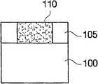
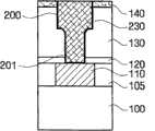
参照图1,所示出的半导体衬底(100)具有第一ILD(层间电介质)层(105)(或绝缘层)以及形成在其上的下部互连线(110)。所述衬底(100)可以是任何半导体器件,比如其中形成有集成电路器件的硅衬底。在一个示例性实施例中,第一ILD层(105)形成在半导体衬底(100)上并且利用镶嵌技术将下部互连线(110)形成在ILD层(105)中。所述下部互连线(110)可以由通常用于形成集成电路导电层的任何适合的材料形成。例如,下部互连线可以包括金属材料,比如铜、铜合金、铝、铝合金、钨或其他适合的金属或导电材料。Referring to FIG. 1, a semiconductor substrate (100) is shown having a first ILD (interlayer dielectric) layer (105) (or insulating layer) and a lower interconnect line (110) formed thereon. The substrate (100) may be any semiconductor device, such as a silicon substrate in which integrated circuit devices are formed. In an exemplary embodiment, a first ILD layer (105) is formed on a semiconductor substrate (100) and a lower interconnect line (110) is formed in the ILD layer (105) using a damascene technique. The lower interconnect lines (110) may be formed from any suitable material commonly used to form conductive layers of integrated circuits. For example, the lower interconnect lines may comprise metallic materials such as copper, copper alloys, aluminum, aluminum alloys, tungsten, or other suitable metallic or conductive materials.
参照图2,在图1的结构上顺序形成蚀刻停止层(120)(或阻挡层)、第二ILD层(130)和盖层(140)(或硬掩模层)。蚀刻停止层(120)用作后续通路蚀刻工艺(以下描述)的蚀刻停止层,以防止下部互连线(110)的暴露。蚀刻停止层(120)还用作扩散阻挡层,以防止/减少金属材料向ILD层(130)中的扩散。蚀刻停止层(120)被制造得尽可能的薄,从而保持绝缘叠层(120和130)的总体低介电特性,同时提供足够的扩散阻挡。在一个示例性实施例中,蚀刻停止层(120)由绝缘材料形成,该绝缘材料具有约300埃至约500埃的厚度并具有相对于ILD层(130)的高蚀刻选择性。例如,蚀刻停止层(120)可以由SiC、SiN、SiCN、SiCO或SiCON形成,并利用已知技术来形成。Referring to FIG. 2 , an etch stop layer ( 120 ) (or barrier layer), a second ILD layer ( 130 ) and a capping layer ( 140 ) (or hard mask layer) are sequentially formed on the structure of FIG. 1 . The etch stop layer (120) serves as an etch stop layer for a subsequent via etch process (described below) to prevent exposure of the lower interconnection line (110). The etch stop layer (120) also acts as a diffusion barrier to prevent/reduce the diffusion of metallic material into the ILD layer (130). The etch stop layer (120) is made as thin as possible to maintain the overall low dielectric properties of the insulating stack (120 and 130) while providing an adequate diffusion barrier. In one exemplary embodiment, the etch stop layer (120) is formed of an insulating material having a thickness of about 300 angstroms to about 500 angstroms and having a high etch selectivity with respect to the ILD layer (130). For example, the etch stop layer (120) may be formed of SiC, SiN, SiCN, SiCO, or SiCON, and formed using known techniques.
在一个示例性实施例中,ILD层(130)优选由k值小于约4.2的低k介电材料形成。ILD层(130)可以由有机聚合物材料或无机材料形成。更具体而言,ILD层(130)可以由掺杂例如碳、氟或氢原子的氧化硅层形成,例如碳氧化硅(SiOC)层、SiOCH层、氟化硅倍半氧化物(fluoro-silses-quioxane,FSQ)层、氢化硅倍半氧化物(hydro-silses-quioxane,HSQ)层、甲基硅倍半氧化物(methyl-silses-quioxane,MSQ)层。无论蚀刻停止层(120)和ILD层(130)使用什么样的材料,ILD层(130)优选由相对于停止层(120)具有高蚀刻选择性并具有低介电常数的材料形成。In an exemplary embodiment, the ILD layer (130) is preferably formed of a low-k dielectric material with a k value of less than about 4.2. The ILD layer (130) may be formed of organic polymer material or inorganic material. More specifically, the ILD layer (130) may be formed of a silicon oxide layer doped with, for example, carbon, fluorine, or hydrogen atoms, such as a silicon oxycarbide (SiOC) layer, a SiOCH layer, a fluoro-silsesquioxide (fluoro-silses -quioxane, FSQ) layer, hydrogenated silicon silsesquioxane (hydro-silses-quioxane, HSQ) layer, methyl-silsesquioxane (methyl-silses-quioxane, MSQ) layer. Regardless of the materials used for the etch stop layer (120) and the ILD layer (130), the ILD layer (130) is preferably formed of a material having high etch selectivity with respect to the stop layer (120) and having a low dielectric constant.
可以形成盖层(140)(或硬掩模层)来保护ILD层(130)在等离子体工艺期间不被损坏并作用对于后续CMP工艺的缓冲层。利用相对于ILD层(130)具有高蚀刻选择性的材料来形成盖层(140)。例如,硬掩模层(140)可以由以下材料形成:(i)绝缘氮化物层,比如氮化硅(SiN)层、碳氮化硅(SiCN)层或氮化硼(BN)层;(ii)绝缘碳化物层,比如碳化硅(SiC)层;(iii)金属氮化物层,比如氮化钽(TaN)层、氮化钛(TiN)层、氮化钨(WN)层或氮化铝(AlN)层;(iv)金属氧化物层,比如氧化铝(Al2O3)层、氧化钽(TaO)层或氧化钛(TiO)层;或者(v)比如SiO2的硅层,或者比如SiOF和SiON的其他材料。A capping layer (140) (or hard mask layer) may be formed to protect the ILD layer (130) from damage during the plasma process and to act as a buffer layer for a subsequent CMP process. The capping layer (140) is formed using a material having high etch selectivity with respect to the ILD layer (130). For example, the hard mask layer (140) may be formed of: (i) an insulating nitride layer, such as a silicon nitride (SiN) layer, a silicon carbonitride (SiCN) layer, or a boron nitride (BN) layer; ( ii) insulating carbide layer, such as silicon carbide (SiC) layer; (iii) metal nitride layer, such as tantalum nitride (TaN) layer, titanium nitride (TiN) layer, tungsten nitride (WN) layer or nitride an aluminum (AlN)layer ; (iv) a metal oxide layer such as an aluminum oxide (Al2O3 ) layer, a tantalum oxide (TaO) layer or a titanium oxide (TiO) layer; or (v) a silicon layer such asSiO2 , Or other materials like SiOF and SiON.
在所述示例性工艺中的下一步骤包括在ILD层(130)中形成通孔。例如,如在图2中所进一步描述的,在盖层(140)上形成ARL(抗反射层)(144),并且形成具有开口(145a)的光致抗蚀剂图案145,通过该开口暴露ARL(144)的一部分表面。开口(145a)与下部互连线(110)对准并且限定了用于形成如图3中所示的通孔(150)的图案。The next step in the exemplary process includes forming vias in the ILD layer (130). For example, as further described in FIG. 2, an ARL (antireflection layer) (144) is formed on the cap layer (140), and a
更具体而言,参照图3,利用光致抗蚀剂图案(145)作为蚀刻掩模,对图2的结构进行一个或多个独立的蚀刻工艺(147),由此依次蚀刻ARL(144)、盖层(140)和ILD层(130),从而形成下至蚀刻停止层(120)的通孔(150)。可以利用任何常规的蚀刻工艺来蚀刻ILD层(130),比如适于蚀刻ILD层(130)的材料的各向异性干法氧化物蚀刻工艺。More specifically, referring to FIG. 3, the structure of FIG. 2 is subjected to one or more separate etching processes (147) using the photoresist pattern (145) as an etch mask, thereby sequentially etching the ARL (144) , a capping layer (140) and an ILD layer (130), thereby forming a via (150) down to the etch stop layer (120). The ILD layer (130) may be etched using any conventional etching process, such as an anisotropic dry oxide etch process suitable for etching the material of the ILD layer (130).
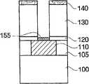
在形成通孔(150)之后,利用例如灰化工艺(O2或H2等离子体)和有机剥离剂来去除光致抗蚀剂图案(145)和ARL(144)。之后,蚀刻通过通孔(150)暴露的蚀刻停止层(120)部分从而暴露一部分下部互连线(110)的表面。图4示出了在去除光致抗蚀剂图案(145)和ARL(144)并且蚀刻部分蚀刻停止层(120)以通过通孔(150)暴露出一部分下部互连线(110)之后的示例性结构。After the via hole (150) is formed, the photoresist pattern (145) and ARL (144) are removed using, for example, an ashing process (O2 orH2 plasma) and an organic stripper. Thereafter, the portion of the etch stop layer (120) exposed through the via hole (150) is etched to expose a portion of the surface of the lower interconnection line (110). Figure 4 shows an example after removing the photoresist pattern (145) and ARL (144) and etching a portion of the etch stop layer (120) to expose a portion of the lower interconnect line (110) through the via hole (150) sexual structure.
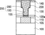
现参照图5,在下部互连线(110)的暴露部分上形成通路盖层(155)。形成该通路盖层(155)以保护下部互连线(110)在后续工艺期间不受等离子体/蚀刻损坏和/或铜氧化的影响。在一个示例性实施例中,该通路盖层(155)形成为具有约50埃至约500埃的厚度。通路盖层(155)优选由具有铜扩散阻挡特性(例如,铜扩散抑制)的材料和/或对于腐蚀或氧化具有抵抗性的材料形成。Referring now to FIG. 5, a via capping layer (155) is formed on the exposed portion of the lower interconnection line (110). The via cap layer (155) is formed to protect the lower interconnect line (110) from plasma/etch damage and/or copper oxidation during subsequent processes. In an exemplary embodiment, the via capping layer (155) is formed to have a thickness of about 50 angstroms to about 500 angstroms. The via cap layer (155) is preferably formed of a material having copper diffusion barrier properties (eg, copper diffusion inhibition) and/or a material that is resistant to corrosion or oxidation.
根据本发明,可以利用各种方法之一在下部互连线(110)的暴露部分上选择性地形成通路盖层(155)。例如,在一个示例性实施例中,可以利用已知的无电沉积方法(例如在美国专利公开No.2002-123220中所公开的方法)来选择性地形成通路盖层(155)。利用无电沉积,通路盖层(155)可以由例如包括CoWP、CoSnP、CoP、CoB、CoSNB、Pd、IN或NiB的材料形成。在另一示例性实施中,可以利用化学气相沉积(CVD)工艺来选择性地形成通路盖层(155)。利用CVD,通路盖层可以由例如包括W、WNx、Ta、TaNx、Ti或TiNx的材料形成。在本发明的又一示例性实施例中,利用原子层沉积(ALD)工艺选择性地形成通路盖层(155)。利用ALD,通路盖层(155)可以由例如包括W、WNx、Ta、TaNx、Ti或TiNx的材料形成。According to the present invention, the via capping layer (155) may be selectively formed on the exposed portion of the lower interconnection line (110) using one of various methods. For example, in one exemplary embodiment, the via capping layer ( 155 ) may be selectively formed using known electroless deposition methods such as those disclosed in US Patent Publication No. 2002-123220. Using electroless deposition, the via capping layer (155) may be formed of materials including, for example, CoWP, CoSnP, CoP, CoB, CoSNB, Pd, IN, or NiB. In another exemplary implementation, the via capping layer ( 155 ) may be selectively formed using a chemical vapor deposition (CVD) process. Using CVD, via capping layers may be formed of materials including, for example, W,WNx , Ta,TaNx , Ti, orTiNx . In yet another exemplary embodiment of the present invention, the via capping layer (155) is selectively formed using an atomic layer deposition (ALD) process. Using ALD, the via capping layer (155) may be formed of materials including, for example, W,WNx , Ta,TaNx , Ti, orTiNx .
参照图6,在形成通路盖层(155)之后,通过沉积一层牺牲材料(162)而用牺牲材料填充通孔(150)。优选地,牺牲材料(162)由具有均匀间隙填充特性的材料形成从而使牺牲材料(162)中空洞的形成最小化。在一个示例性实施例中,牺牲材料(162)由有机旋涂聚合物(SOP)材料形成,比如聚亚芳基醚(polyaryleneether)基材料、聚甲基丙烯酸甲酯(polymetamethylacrylat)基材料或乙烯基醚甲基丙稀酸酯(vinylethermetacrylate)基材料。在本发明的另一示例性实施例中,牺牲材料(162)由无机旋涂玻璃(SOG)材料形成,比如HSQ(氢化硅倍半氧化物HydrogenSilsesQuioxane)基材料、MSQ(甲基硅倍半氧化物MethylSilsesQuioxane)基材料。Referring to FIG. 6, after the via capping layer (155) is formed, the via hole (150) is filled with a sacrificial material by depositing a layer of sacrificial material (162). Preferably, the sacrificial material (162) is formed of a material having uniform gap-fill properties to minimize the formation of voids in the sacrificial material (162). In one exemplary embodiment, the sacrificial material (162) is formed of an organic spin-on polymer (SOP) material, such as polyarylene ether (polyaryleneether) based material, polymetamethylacrylat (polymetamethylacrylat) based material or vinyl Base ether methacrylate (vinylethermetacrylate) based materials. In another exemplary embodiment of the present invention, the sacrificial material (162) is formed of an inorganic spin-on-glass (SOG) material, such as HSQ (HydrogenSilsesquioxideHydrogenSilsesQuioxane) based material, MSQ (Methylsilsesquioxide MethylSilsesQuioxane)-based materials.
优选选取牺牲材料(162)使其具有与形成ILD层(130)的介电材料的干法蚀刻特性相似的干法蚀刻特性。例如,对于给定的干法蚀刻化学品,牺牲材料(162)优选具有比ILD层(130)的干法蚀刻速率略快的干法蚀刻速率。正如以下所说明的,这确保了在形成沟槽区域之后在通孔(150)中留下足够量的牺牲材料。此外,选择牺牲材料(162)使其具有比ILD层(130)的湿法蚀刻速率明显快的湿法蚀刻速率。正如以下所说明的,这能够在形成沟槽区域之后去除通孔(150)中的剩余牺牲材料。使用SOP还是SOG材料取决于形成ILD层(130)的材料,以及对于给定的蚀刻化学品,ILD层(130)与牺牲材料(162)之间的所需的蚀刻选择性。The sacrificial material (162) is preferably selected to have dry etch properties similar to the dry etch properties of the dielectric material forming the ILD layer (130). For example, for a given dry etch chemistry, the sacrificial material (162) preferably has a dry etch rate slightly faster than the dry etch rate of the ILD layer (130). As explained below, this ensures that a sufficient amount of sacrificial material remains in the via (150) after the trench region is formed. Additionally, the sacrificial material (162) is selected to have a wet etch rate that is significantly faster than the wet etch rate of the ILD layer (130). As explained below, this enables the removal of remaining sacrificial material in the via (150) after formation of the trench region. Whether a SOP or SOG material is used depends on the material forming the ILD layer (130), and the desired etch selectivity between the ILD layer (130) and the sacrificial material (162) for a given etch chemistry.
在所述示例性工艺中的下一步骤是在ILD层(130)中形成沟槽区域。参照图7,所述示例性工艺从在牺牲材料层(162)上形成第二ARL(抗反射层)(184)开始,并形成具有开口(185a)的第二光致抗蚀剂图案(185),通过该开口(185a)暴露第二ARL(184)的一部分表面。开口(185a)形成为与通孔(150)对准,并且开口(185a)限定了用于在ILD层(130)中形成沟槽的蚀刻图案,如以下所说明的。The next step in the exemplary process is to form trench regions in the ILD layer (130). Referring to FIG. 7, the exemplary process starts with forming a second ARL (Anti-Reflection Layer) (184) on the sacrificial material layer (162), and forms a second photoresist pattern (185) with openings (185a). ) through which a portion of the surface of the second ARL (184) is exposed. The opening (185a) is formed in alignment with the via (150), and the opening (185a) defines an etch pattern for forming trenches in the ILD layer (130), as explained below.
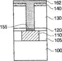
参照图8,执行蚀刻工艺(227),从而通过利用光致抗蚀剂图案(185)作为蚀刻掩模依次蚀刻ARL(184)、牺牲材料(162)和ILD层(130)而形成沟槽(190)。在一种示例性方法中,利用干法蚀刻工艺来进行蚀刻(227),该干法蚀刻工艺具有适于蚀刻形成不同层的材料类型的蚀刻化学品。如以上所提到的,选择用于蚀刻沟槽(190)的干法蚀刻化学品使得牺牲材料(162)以比ILD层(130)更快的速率被蚀刻,从而避免缺陷的形成。更具体而言,执行蚀刻使得牺牲材料(162)与ILD(130)之间的蚀刻速率基本相同或者小于10∶1。进行足够时间的蚀刻工艺从而形成在ILD层(130)的顶表面之下具有所需沟槽深度的沟槽(190)。在干法蚀刻工艺期间,通孔(150)中剩余的牺牲材料(162a)凹进到沟槽(190)的底部之下,从而形成包括沟槽(190)和部分通孔(150)的非填充区域(195)。8, an etching process (227) is performed to form trenches by sequentially etching the ARL (184), the sacrificial material (162) and the ILD layer (130) using the photoresist pattern (185) as an etching mask ( 190). In one exemplary method, the etching (227) is performed using a dry etching process with an etching chemistry suitable for etching the type of material forming the different layers. As mentioned above, the dry etch chemistry used to etch the trenches (190) is chosen such that the sacrificial material (162) is etched at a faster rate than the ILD layer (130), thereby avoiding the formation of defects. More specifically, etching is performed such that the etch rate between the sacrificial material (162) and the ILD (130) is substantially the same or less than 10:1. The etch process is performed for a sufficient time to form a trench (190) with the desired trench depth below the top surface of the ILD layer (130). During the dry etching process, the remaining sacrificial material (162a) in the via (150) is recessed below the bottom of the trench (190), thereby forming a non- Fill area (195).
图9是在剩余牺牲材料(162、162a)以及光致抗蚀剂(185)和ARL(184)被去除之后图8的结构的示意性侧视图。在一个示例性实施例中,利用例如灰化工艺来去除第二光致抗蚀剂图案(185)和ARL(184),之后去除牺牲材料(162)。如果牺牲材料(162)包括有机材料,则将牺牲材料(162)与第二光致抗蚀剂图案(185)一起去除。当牺牲材料(162)是无机SOG材料时,在去除光致抗蚀剂图案(185)和ARL(184)之后,利用湿法蚀刻工艺来去除形成在硬掩模层(140)上的牺牲材料以及剩余在通孔(150)中的牺牲材料(162a)。如上所述,选择湿法蚀刻化学品(例如HF溶液),使得牺牲材料以比ILD层(130)明显快的速率被选择性地蚀刻。例如,如果牺牲材料(162)由SOG层(比如HSQ层)形成并且ILD层(130)由SiOC形成,则在HF溶液中,牺牲材料(162)被蚀刻得明显快于ILD层(130)。简言之,选择湿法化学品从而在牺牲材料(162)与ILD层(130)的材料之间提供高的选择性。Figure 9 is a schematic side view of the structure of Figure 8 after the remaining sacrificial material (162, 162a) and photoresist (185) and ARL (184) have been removed. In one exemplary embodiment, the second photoresist pattern ( 185 ) and the ARL ( 184 ) are removed using, for example, an ashing process, followed by removal of the sacrificial material ( 162 ). If the sacrificial material (162) includes an organic material, the sacrificial material (162) is removed together with the second photoresist pattern (185). When the sacrificial material (162) is an inorganic SOG material, after removing the photoresist pattern (185) and the ARL (184), a wet etching process is utilized to remove the sacrificial material formed on the hard mask layer (140) and the sacrificial material (162a) remaining in the via (150). As mentioned above, the wet etch chemistry (eg HF solution) is selected such that the sacrificial material is selectively etched at a significantly faster rate than the ILD layer (130). For example, if the sacrificial material (162) is formed from a SOG layer (such as a HSQ layer) and the ILD layer (130) is formed from SiOC, then the sacrificial material (162) is etched significantly faster than the ILD layer (130) in HF solution. In short, the wet process chemistry is chosen to provide high selectivity between the sacrificial material (162) and the material of the ILD layer (130).
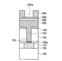
所述示例性方法的下一步骤包括通过用比如铜的导电材料填充沟槽(190)和通孔(150)而形成上部金属互连(双镶嵌互连)。图10A和10B描绘了用于该工艺的各种示例性实施例,其中在通路盖层(155)上方形成互连结构(230)(图10A),并且其中在去除通路盖层(155)之后形成互连结构(230)。The next step of the exemplary method includes forming an upper metal interconnect (dual damascene interconnect) by filling the trenches (190) and vias (150) with a conductive material such as copper. Figures 10A and 10B depict various exemplary embodiments for this process, wherein the interconnect structure (230) is formed over the via capping layer (155) (Fig. 10A), and wherein after the via capping layer (155) is removed An interconnect structure is formed (230).
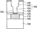
更具体而言,在一个实施例中,参照图10A,形成上部互连结构(230)的方法包括在沟槽(190)和通孔(150)的侧壁上以及通路盖层(155)的表面上形成共形的阻挡层(200)。在一个示例性实施例中,可以利用溅射沉积工艺形成阻挡层(200),从而利用比如TiN或TaN的材料形成厚度为约50埃至约500埃的阻挡层。之后,在共形阻挡层(200)的上方沉积一层导电材料,从而利用该导电材料填充通孔(150)和沟槽(190)。例如,所述导电材料可以是利用常规的电镀工艺沉积的铜。然后执行平坦化工艺(例如CMP)从而使所述结构的顶表面下至硬掩模层(140)平坦化,由此完成具有双镶嵌结构的金属布线层(230)的形成。More specifically, in one embodiment, referring to FIG. 10A , the method of forming the upper interconnect structure (230) includes on the sidewalls of the trench (190) and the via (150) and the A conformal barrier layer (200) is formed on the surface. In one exemplary embodiment, the barrier layer ( 200 ) may be formed using a sputter deposition process such that a material such as TiN or TaN is used to form the barrier layer to a thickness of about 50 angstroms to about 500 angstroms. Thereafter, a layer of conductive material is deposited over the conformal barrier layer (200), thereby filling the vias (150) and trenches (190) with the conductive material. For example, the conductive material may be copper deposited using a conventional electroplating process. A planarization process (such as CMP) is then performed to planarize the top surface of the structure down to the hard mask layer (140), thereby completing the formation of the metal wiring layer (230) having a dual damascene structure.
在本发明的另一示例性实施例中,参照图10B,形成上部互连结构(230)的工艺包括在沟槽(190)和通孔(150)的侧壁上以及通路盖层(155)的表面上形成第一共形的阻挡层(200),然后蚀刻通孔(150)的底层从而去除通路盖层(155)和通路盖层(155)表面上的部分第一共形阻挡层,由此暴露一部分下部互连线(110)。在一个示例性实施例中,可以利用比如Ar溅射的溅射工艺来去除通路盖层(155)及其表面上的第一共形阻挡层(200)。此外,可以执行Ar溅射从而去除下部互连线(110)上表面的薄层,以去除可能存在的损坏区域。In another exemplary embodiment of the present invention, referring to FIG. 10B , the process of forming the upper interconnection structure (230) includes on the trenches (190) and the sidewalls of the vias (150) and via capping layers (155) Forming a first conformal barrier layer (200) on the surface of the via hole (150) and then etching the bottom layer of the via hole (150) to remove the via cover layer (155) and part of the first conformal barrier layer on the surface of the via cover layer (155), A portion of the lower interconnection line (110) is thereby exposed. In an exemplary embodiment, the via capping layer (155) and the first conformal barrier layer (200) on its surface may be removed using a sputtering process such as Ar sputtering. In addition, Ar sputtering may be performed to remove a thin layer on the upper surface of the lower interconnect (110) to remove possible damaged areas.
然后,在第一共形阻挡层(200)和下部互连线(110)的暴露部分上形成第二共形阻挡层(201),之后在第二共形阻挡层(201)上方沉积一层导电材料,从而利用该导电材料填充通孔(150)和沟槽(190)。之后,平坦化所得结构(例如通过CMP),从而去除下至硬掩模层(140)表面的导电材料和阻挡材料,由此完成双镶嵌结构(230)的形成。Then, a second conformal barrier layer (201) is formed on the exposed portion of the first conformal barrier layer (200) and the lower interconnect line (110), and then a layer is deposited over the second conformal barrier layer (201) The conductive material is used to fill the vias (150) and trenches (190) with the conductive material. Thereafter, the resulting structure is planarized (eg, by CMP), thereby removing conductive and barrier materials down to the surface of the hard mask layer (140), thereby completing the formation of the dual damascene structure (230).
以上参照图1至图10A/10B描述的示例性方法是通路第一双镶嵌方法(via first dual damascene,VFDD),该方法利用单层抗蚀剂(SLR)工艺来执行。利用示例性的VFDD SLR方法,牺牲材料可以是无机或有机材料。在本发明的其他示例性实施例中,提供了VFDD多层抗蚀剂(MLR)方法,这将参照图11至18A/18B的示例图来描述。利用这些示例性方法,牺牲材料由有机材料形成从而在蚀刻工艺期间用作光致抗蚀剂。首先参照图11描述图11至18A/18B的示例性方法,但应理解的是,以上参照图1至5描述的示例性方法是可以在图11的处理步骤之前的处理步骤。The exemplary method described above with reference to FIGS. 1 to 10A/10B is a via first dual damascene (VFDD) method, which is performed using a single layer resist (SLR) process. With the exemplary VFDD SLR approach, the sacrificial material can be inorganic or organic. In other exemplary embodiments of the present invention, a VFDD multilayer resist (MLR) method is provided, which will be described with reference to the exemplary diagrams of FIGS. 11 to 18A/18B. With these exemplary methods, the sacrificial material is formed from an organic material to serve as a photoresist during the etching process. The example method of FIGS. 11-18A/18B is first described with reference to FIG. 11 , but it should be understood that the example method described above with reference to FIGS. 1-5 is a processing step that may precede that of FIG. 11 .
参照图11,在形成通路盖层(155)之后(例如图5),通过沉积牺牲材料(262)层用牺牲材料填充通孔(150),从而填充通孔(150)。优选地,牺牲材料(262)由具有均匀间隙填充特性的材料形成从而使牺牲材料(262)中空洞的形成最小化。在一个示例性实施例中,牺牲材料(262)由有机旋涂聚合物(SOP)材料形成,比如聚亚芳基醚基材料、聚甲基丙烯酸甲酯基材料或乙烯基醚甲基丙稀酸酯基材料。正如以上描述的示例性实施例,优选选取牺牲材料(262)使其相对于形成ILD层(130)的介电材料具有给定的干法和湿法蚀刻特性,从而在以下描述的后续处理步骤中,对于蚀刻沟槽区域和去除剩余的牺牲材料实现所需的蚀刻选择性。Referring to FIG. 11 , after via capping layer ( 155 ) is formed (eg, FIG. 5 ), via ( 150 ) is filled with sacrificial material by depositing a layer of sacrificial material ( 262 ). Preferably, the sacrificial material (262) is formed of a material having uniform gap-fill properties to minimize the formation of voids in the sacrificial material (262). In one exemplary embodiment, the sacrificial material (262) is formed from an organic spin-on polymer (SOP) material, such as polyarylene ether based material, polymethyl methacrylate based material, or vinyl ether methacrylic Ester based materials. As in the exemplary embodiment described above, the sacrificial material (262) is preferably selected to have given dry and wet etch characteristics relative to the dielectric material forming the ILD layer (130), so that it can be used in subsequent processing steps described below. , the desired etch selectivity is achieved for etching the trench region and removing remaining sacrificial material.
比较图11和图6的示例图,可注意到图11中的牺牲材料(262)层形成得比图6所示的牺牲材料(162)层更厚。在本示例性实施例中将牺牲材料(262)形成得足够厚,因为正如以下将说明的(图16),在后续蚀刻工艺期间,将牺牲材料(262)层用作蚀刻掩模。Comparing the example diagrams of FIG. 11 and FIG. 6, it can be noted that the layer of sacrificial material (262) in FIG. 11 is formed thicker than the layer of sacrificial material (162) shown in FIG. The sacrificial material (262) is formed thick enough in this exemplary embodiment because, as will be explained below (FIG. 16), the sacrificial material (262) layer is used as an etch mask during the subsequent etching process.
参照图12,在牺牲材料(262)层上形成硬掩模层(282)。硬掩模层(282)可以是氧化硅层、氮化硅层、碳化硅层、SiON、SiCN、SiOCN、Ta、TaN、Ti、TiN、Al2O3、BQ、HSQ。选择形成硬掩模层(282)的材料使其相对于牺牲材料(262)具有高的蚀刻选择性。Referring to FIG. 12, a hard mask layer (282) is formed on the layer of sacrificial material (262). The hard mask layer (282) can be a silicon oxide layer, a silicon nitride layer, a siliconcarbide layer, SiON, SiCN, SiOCN, Ta, TaN, Ti, TiN,Al2O3 , BQ, HSQ. The material forming the hard mask layer (282) is selected to have high etch selectivity relative to the sacrificial material (262).
参照图13,在硬掩模层(282)上形成ARL(抗反射层)(284),并形成具有开口(285a)的光致抗蚀剂图案(285),通过该开口(285a)暴露ARL(284)的一部分表面。开口(285a)形成为与通孔(150)对准,并且开口(285a)限定了用于在ILD层(130)中形成沟槽区域的蚀刻图案。Referring to FIG. 13, an ARL (anti-reflection layer) (284) is formed on a hard mask layer (282), and a photoresist pattern (285) is formed having an opening (285a) through which the ARL is exposed. Part of the surface of (284). The opening (285a) is formed in alignment with the via (150), and the opening (285a) defines an etch pattern for forming a trench region in the ILD layer (130).
参照图14,利用光致抗蚀剂图案(285)作为蚀刻掩模执行一个或多个蚀刻工艺(307),从而依次蚀刻通过开口(285a)暴露的部分ARL(284)和硬掩模层(282)。在一个示例性实施例中,利用光致抗蚀剂图案(285)作为蚀刻掩模来执行蚀刻工艺(307),由此依次蚀刻ARL(284)和硬掩模层(282)。优选地,利用单一干法蚀刻工艺来执行蚀刻工艺(307),该干法蚀刻工艺利用了适于蚀刻形成不同层(284)和(282)的材料类型的蚀刻化学品。Referring to FIG. 14, one or more etching processes (307) are performed using the photoresist pattern (285) as an etch mask, thereby sequentially etching the portion of the ARL (284) exposed through the opening (285a) and the hard mask layer ( 282). In one exemplary embodiment, an etching process ( 307 ) is performed using the photoresist pattern ( 285 ) as an etching mask, thereby sequentially etching the ARL ( 284 ) and the hard mask layer ( 282 ). Preferably, the etch process (307) is performed using a single dry etch process utilizing etch chemistries suitable for etching the types of materials forming the different layers (284) and (282).
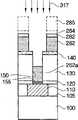
参照图15,执行给定时间的第二蚀刻工艺(317),从而蚀刻通过开口(285a)暴露的牺牲材料(262)。利用造成光致抗蚀剂图案(285)和ARL(284)被去除同时蚀刻牺牲材料(262)的蚀刻化学品来执行第二蚀刻工艺(317)。在一个示例性实施例中,利用干法蚀刻工艺来执行第二蚀刻工艺(317),该干法蚀刻工艺利用了适于蚀刻形成不同层的材料类型的蚀刻化学品。优选选择所述干法蚀刻化学品使得牺牲材料(262)以比ILD层(130)更快的速率被蚀刻,以避免缺陷的形成。更具体而言,执行蚀刻使得牺牲材料(262)与ILD(130)之间的蚀刻速率基本相同或者小于10∶1。如图15所描绘的,执行第二蚀刻工艺(317)从而蚀刻牺牲材料(262a)下至通孔(150)中的水平面,该水平面与预期沟槽的水平面相同或者低于预期沟槽的水平面。利用示例性蚀刻工艺(317),暴露了图案化的硬掩模层(282)。Referring to FIG. 15, a second etching process (317) is performed for a given time, thereby etching the sacrificial material (262) exposed through the opening (285a). A second etch process (317) is performed using an etch chemistry that causes the photoresist pattern (285) and ARL (284) to be removed while etching the sacrificial material (262). In one exemplary embodiment, the second etch process (317) is performed using a dry etch process utilizing etch chemistries suitable for etching the types of materials forming the different layers. The dry etch chemistry is preferably selected such that the sacrificial material (262) is etched at a faster rate than the ILD layer (130) to avoid defect formation. More specifically, the etch is performed such that the etch rate between the sacrificial material (262) and the ILD (130) is substantially the same or less than 10:1. As depicted in Figure 15, a second etch process (317) is performed to etch the sacrificial material (262a) down to a level in the via (150) that is the same as or lower than the level of the intended trench . Using an exemplary etch process (317), the patterned hard mask layer (282) is exposed.
参照图16,利用图案化的硬掩模层(282)和牺牲材料层(262)作为蚀刻掩模,执行第三蚀刻工艺(327),以蚀刻盖层(140)和ILD层(130)的暴露部分从而形成沟槽(290)。在该示例性实施例中,蚀刻盖层(140)和ILD层(130)的暴露部分,从而将沟槽(290)形成至ILD层(130)顶表面之下的预期水平面。Referring to FIG. 16, using the patterned hard mask layer (282) and the sacrificial material layer (262) as an etching mask, a third etching process (327) is performed to etch the capping layer (140) and the ILD layer (130). Portions are exposed thereby forming trenches (290). In this exemplary embodiment, exposed portions of the cap layer (140) and ILD layer (130) are etched, thereby forming trenches (290) to a desired level below the top surface of the ILD layer (130).
在一种示例性方法中,利用相对于牺牲材料(262)对硬掩模层(282)、盖层(140)和ILD层(130)具有高度选择性的蚀刻化学品来执行蚀刻(327)。以这样的方式,以比牺牲材料(262)明显大的速率来蚀刻盖层(140)和ILD层(130),使得在蚀刻掉硬掩模层(282)之后,使盖层(140)之上的牺牲材料(262)用作蚀刻掩模,并使得通孔(150)底部中的牺牲材料(262a)不被过蚀刻,由此保护通路盖层(155)和下部互连线(110),使其不暴露于蚀刻气氛。例如,如图16中所描绘的,在该蚀刻工艺(327)期间,蚀刻掉相对少量的牺牲材料(262b)。In one exemplary method, etching (327) is performed using an etch chemistry that is highly selective for the hard mask layer (282), capping layer (140), and ILD layer (130) relative to the sacrificial material (262) . In such a manner, the capping layer (140) and ILD layer (130) are etched at a rate significantly greater than the sacrificial material (262), such that after the hard mask layer (282) is etched away, the capping layer (140) The sacrificial material (262) on the via hole (150) is used as an etch mask, and the sacrificial material (262a) in the bottom of the via hole (150) is not over-etched, thereby protecting the via cover layer (155) and the lower interconnect line (110) , so that it is not exposed to the etching atmosphere. For example, as depicted in Figure 16, during this etch process (327), a relatively small amount of sacrificial material (262b) is etched away.
在一个示例性实施例中,利用干法蚀刻工艺来执行蚀刻工艺(327),该干法蚀刻工艺具有被选取的蚀刻化学品使得牺牲材料(262a、262)以比ILD层(130)更低的速率被蚀刻,从而避免缺陷的形成。更具体而言,执行蚀刻使得牺牲材料(262a、262)与ILD层(130)之间的蚀刻速率基本快于1∶10。In one exemplary embodiment, the etch process (327) is performed using a dry etch process with etch chemistries selected such that the sacrificial material (262a, 262) is lower than the ILD layer (130). The rate is etched, thus avoiding the formation of defects. More specifically, the etch is performed such that the etch rate between the sacrificial material (262a, 262) and the ILD layer (130) is substantially faster than 1:10.
接下来,去除剩余的牺牲材料(262a、262)(图16中所描绘的)以暴露盖层(140)和通路盖层(155)。图17是在去除剩余的牺牲材料(262、262a)之后图16的结构的示意性侧视图。可以利用例如灰化工艺或者其他蚀刻方法来去除牺牲材料(262、262a),所述其他蚀刻方法具有这样的蚀刻化学品,该蚀刻化学品能够使形成牺牲材料(262)的有机材料以相对大于形成ILD层(130)的材料的蚀刻速率的速率被蚀刻。Next, the remaining sacrificial material (262a, 262) (depicted in Figure 16) is removed to expose the capping layer (140) and via capping layer (155). Figure 17 is a schematic side view of the structure of Figure 16 after removal of the remaining sacrificial material (262, 262a). The sacrificial material (262, 262a) may be removed using, for example, an ashing process or other etching methods having etch chemistries that enable the organic material forming the sacrificial material (262) to be removed in a relatively larger The rate of the etch rate of the material forming the ILD layer (130) is etched.
所述示例性方法的下一步骤包括通过用比如铜的导电材料填充沟槽(290)和通孔(150)来形成上部金属互连(双镶嵌互连)。从图17中描绘的示例性结构开始,以上参照图10A和10B描述的相同的制造方法可以用于形成图18A和18B中所描绘的结构。The next step of the exemplary method includes forming an upper metal interconnect (dual damascene interconnect) by filling the trenches (290) and vias (150) with a conductive material such as copper. Starting with the exemplary structure depicted in Figure 17, the same fabrication methods described above with reference to Figures 10A and 10B can be used to form the structure depicted in Figures 18A and 18B.
尽管此处已经参照附图描述了示例性实施例,但应理解的是,本发明不限于此处描述的示例性实施例,在不偏离本发明的范围或主旨的前提下,本领域普通技术人员可以容易地构想各种其他变化和修改。所有这些变化和修改意于包括在所附权利要求所界定的本发明的范围内。Although the exemplary embodiments have been described herein with reference to the accompanying drawings, it should be understood that the present invention is not limited to the exemplary embodiments described herein, and that those of ordinary skill in the art can be used without departing from the scope or spirit of the invention. Various other changes and modifications can be readily devised by the person. All such changes and modifications are intended to be included within the scope of the present invention as defined in the appended claims.
Claims (42)
Translated fromChineseApplications Claiming Priority (3)
| Application Number | Priority Date | Filing Date | Title |
|---|---|---|---|
| KR10981/05 | 2005-02-05 | ||
| KR1020050010981AKR100690881B1 (en) | 2005-02-05 | 2005-02-05 | A microelectronic device having a method for manufacturing dual damascene wiring of a microelectronic device and the dual damascene wiring manufactured thereby |
| US11/223,311 | 2005-09-09 |
Publications (2)
| Publication Number | Publication Date |
|---|---|
| CN1835206A CN1835206A (en) | 2006-09-20 |
| CN100576494Ctrue CN100576494C (en) | 2009-12-30 |
Family
ID=36780501
Family Applications (1)
| Application Number | Title | Priority Date | Filing Date |
|---|---|---|---|
| CN200610007141AActiveCN100576494C (en) | 2005-02-05 | 2006-02-05 | Method for forming dual damascene wiring of semiconductor device using protective via capping layer |
Country Status (4)
| Country | Link |
|---|---|
| US (1) | US7541276B2 (en) |
| KR (1) | KR100690881B1 (en) |
| CN (1) | CN100576494C (en) |
| TW (1) | TWI362087B (en) |
Families Citing this family (41)
| Publication number | Priority date | Publication date | Assignee | Title |
|---|---|---|---|---|
| KR100652317B1 (en)* | 2005-08-11 | 2006-11-29 | 동부일렉트로닉스 주식회사 | Method for manufacturing metal pad of semiconductor device |
| KR100703561B1 (en)* | 2005-12-28 | 2007-04-03 | 동부일렉트로닉스 주식회사 | Dual damascene pattern formation method of semiconductor device |
| US7800228B2 (en)* | 2006-05-17 | 2010-09-21 | International Business Machines Corporation | Reliable via contact interconnect structure |
| DE102006056626B4 (en) | 2006-11-30 | 2024-12-19 | Advanced Micro Devices, Inc. | Method for forming an opening in a metallization structure of a semiconductor device using a self-limiting deposition process |
| CN101202244B (en)* | 2006-12-15 | 2010-06-09 | 中芯国际集成电路制造(上海)有限公司 | Method for removing photoresist graph in forming process of dual embedded structure |
| US7521358B2 (en)* | 2006-12-26 | 2009-04-21 | Lam Research Corporation | Process integration scheme to lower overall dielectric constant in BEoL interconnect structures |
| US7888798B2 (en)* | 2007-05-16 | 2011-02-15 | Samsung Electronics Co., Ltd. | Semiconductor devices including interlayer conductive contacts and methods of forming the same |
| CN101355047B (en)* | 2007-07-27 | 2010-05-19 | 中芯国际集成电路制造(上海)有限公司 | Method for forming through hole in low dielectric coefficient medium layer |
| KR100880233B1 (en)* | 2007-08-29 | 2009-01-28 | 주식회사 동부하이텍 | Metal wiring formation method |
| KR100898222B1 (en)* | 2007-08-30 | 2009-05-18 | 주식회사 동부하이텍 | Semiconductor device and manufacturing method thereof |
| US8148269B2 (en)* | 2008-04-04 | 2012-04-03 | Applied Materials, Inc. | Boron nitride and boron-nitride derived materials deposition method |
| JP2010021296A (en)* | 2008-07-10 | 2010-01-28 | Panasonic Corp | Manufacturing method of semiconductor device |
| US8288276B2 (en)* | 2008-12-30 | 2012-10-16 | International Business Machines Corporation | Method of forming an interconnect structure including a metallic interfacial layer located at a bottom via portion |
| US8722537B2 (en)* | 2009-03-19 | 2014-05-13 | Taiwan Semiconductor Manufacturing Company, Ltd. | Multi-sacrificial layer and method |
| CN102044523B (en)* | 2009-10-14 | 2012-08-22 | 无锡华润上华半导体有限公司 | Semiconductor device structure and manufacturing method thereof |
| CN102403263B (en)* | 2010-09-17 | 2014-06-04 | 中芯国际集成电路制造(北京)有限公司 | Trench etching method in double Damascus structure |
| CN102468265A (en)* | 2010-11-01 | 2012-05-23 | 中芯国际集成电路制造(上海)有限公司 | Connection plug and manufacturing method thereof |
| KR101732975B1 (en)* | 2010-12-03 | 2017-05-08 | 삼성전자주식회사 | Method of manufacturing a semiconductor device |
| US8461683B2 (en)* | 2011-04-01 | 2013-06-11 | Intel Corporation | Self-forming, self-aligned barriers for back-end interconnects and methods of making same |
| CN102760684A (en)* | 2011-04-26 | 2012-10-31 | 中芯国际集成电路制造(上海)有限公司 | Metal interconnection method |
| CN102443830A (en)* | 2011-10-12 | 2012-05-09 | 上海华力微电子有限公司 | Method for improving copper electroplating process |
| US9396990B2 (en) | 2013-01-31 | 2016-07-19 | Taiwan Semiconductor Manufacturing Co., Ltd. | Capping layer for improved deposition selectivity |
| JP6049527B2 (en)* | 2013-04-05 | 2016-12-21 | 東京エレクトロン株式会社 | Plasma processing method and plasma processing apparatus |
| CN104377160B (en)* | 2013-08-14 | 2017-05-03 | 华邦电子股份有限公司 | Metal interconnection structure and its technology |
| EP3238236B1 (en)* | 2014-12-23 | 2021-12-15 | Intel Corporation | Via blocking layer |
| EP3238235A4 (en)* | 2014-12-23 | 2018-07-25 | Intel Corporation | Decoupled via fill |
| US9793212B2 (en) | 2015-04-16 | 2017-10-17 | Taiwan Semiconductor Manufacturing Company, Ltd. | Interconnect structures and methods of forming same |
| US9859156B2 (en)* | 2015-12-30 | 2018-01-02 | Taiwan Semiconductor Manufacturing Co., Ltd. | Interconnection structure with sidewall dielectric protection layer |
| US9768063B1 (en)* | 2016-06-30 | 2017-09-19 | Lam Research Corporation | Dual damascene fill |
| US10043740B2 (en) | 2016-07-12 | 2018-08-07 | Intel Coporation | Package with passivated interconnects |
| US9805972B1 (en)* | 2017-02-20 | 2017-10-31 | Globalfoundries Inc. | Skip via structures |
| US10312188B1 (en)* | 2018-01-11 | 2019-06-04 | Globalfoundries Inc. | Interconnect structure with method of forming the same |
| KR102592854B1 (en) | 2018-04-06 | 2023-10-20 | 삼성전자주식회사 | Semiconductor device and Method for fabricating thereof |
| US10784151B2 (en)* | 2018-09-11 | 2020-09-22 | Taiwan Semiconductor Manufacturing Company Ltd. | Interconnect structure and manufacturing method for the same |
| US10943791B2 (en)* | 2018-10-31 | 2021-03-09 | Taiwan Semiconductor Manufacturing Co., Ltd. | Pattern formation method and method for manufacturing a semiconductor device |
| US11164815B2 (en)* | 2019-09-28 | 2021-11-02 | International Business Machines Corporation | Bottom barrier free interconnects without voids |
| KR102845461B1 (en)* | 2019-11-27 | 2025-08-11 | 삼성전자주식회사 | interconnection structure of integrated circuit semiconductor device |
| US11488859B2 (en)* | 2019-12-27 | 2022-11-01 | Taiwan Semiconductor Manufacturing Company, Ltd. | Semiconductor device and method |
| CN114496904B (en)* | 2020-10-27 | 2024-12-06 | 长鑫存储技术有限公司 | Method for forming semiconductor structure |
| US20230178474A1 (en)* | 2021-12-07 | 2023-06-08 | International Business Machines Corporation | Beol interconnect subtractive etch super via |
| TWI840818B (en)* | 2022-03-31 | 2024-05-01 | 南亞科技股份有限公司 | Method for reworking semiconductor device |
Family Cites Families (27)
| Publication number | Priority date | Publication date | Assignee | Title |
|---|---|---|---|---|
| KR100385946B1 (en) | 1999-12-08 | 2003-06-02 | 삼성전자주식회사 | Method for forming a metal layer by an atomic layer deposition and a semiconductor device with the metal layer as a barrier metal layer, an upper electrode, or a lower electrode of capacitor |
| US6140226A (en) | 1998-01-16 | 2000-10-31 | International Business Machines Corporation | Dual damascene processing for semiconductor chip interconnects |
| JP2000156406A (en) | 1998-11-19 | 2000-06-06 | Sony Corp | Semiconductor device and its manufacture |
| TW495910B (en) | 1999-07-16 | 2002-07-21 | Taiwan Semiconductor Mfg | Manufacturing method of dual damascene structure |
| US6297149B1 (en)* | 1999-10-05 | 2001-10-02 | International Business Machines Corporation | Methods for forming metal interconnects |
| TW461028B (en) | 2000-08-14 | 2001-10-21 | Taiwan Semiconductor Mfg | Method for manufacturing dual damascene structure |
| US6383920B1 (en)* | 2001-01-10 | 2002-05-07 | International Business Machines Corporation | Process of enclosing via for improved reliability in dual damascene interconnects |
| US6603204B2 (en) | 2001-02-28 | 2003-08-05 | International Business Machines Corporation | Low-k interconnect structure comprised of a multilayer of spin-on porous dielectrics |
| US6579793B2 (en) | 2001-03-27 | 2003-06-17 | Sharp Laboratories Of America, Inc. | Method of achieving high adhesion of CVD copper thin films on TaN Substrates |
| US6664182B2 (en) | 2001-04-25 | 2003-12-16 | Macronix International Co. Ltd. | Method of improving the interlayer adhesion property of low-k layers in a dual damascene process |
| TW516180B (en) | 2001-05-17 | 2003-01-01 | Silicon Integrated Sys Corp | Manufacturing method for dual damascene structure of integrated circuit |
| TW494534B (en) | 2001-05-25 | 2002-07-11 | United Microelectronics Corp | Method of fabricating a dual damascene structure |
| TW521385B (en) | 2001-05-28 | 2003-02-21 | United Microelectronics Corp | Method for forming via-first dual damascene interconnect structure |
| US6506692B2 (en)* | 2001-05-30 | 2003-01-14 | Intel Corporation | Method of making a semiconductor device using a silicon carbide hard mask |
| US6458705B1 (en) | 2001-06-06 | 2002-10-01 | United Microelectronics Corp. | Method for forming via-first dual damascene interconnect structure |
| TW508741B (en) | 2001-06-07 | 2002-11-01 | United Microelectronics Corp | Method for manufacturing dual damascene structure |
| TW516182B (en) | 2002-01-23 | 2003-01-01 | Taiwan Semiconductor Mfg | Manufacturing method of dual damascene structure |
| US6689695B1 (en)* | 2002-06-28 | 2004-02-10 | Taiwan Semiconductor Manufacturing Company | Multi-purpose composite mask for dual damascene patterning |
| KR100475931B1 (en)* | 2002-07-02 | 2005-03-10 | 매그나칩 반도체 유한회사 | Method for manufacturing a multi metal line in semiconductor device |
| TW574745B (en) | 2002-09-05 | 2004-02-01 | Taiwan Semiconductor Mfg | A dual damascene process applying porous low-k dielectric |
| US7109119B2 (en)* | 2002-10-31 | 2006-09-19 | Taiwan Semiconductor Manufacturing Company, Ltd. | Scum solution for chemically amplified resist patterning in cu/low k dual damascene |
| US6995085B2 (en) | 2003-01-17 | 2006-02-07 | Taiwan Semiconductor Manufacturing Company, Ltd. | Underlayer protection for the dual damascene etching |
| JP3992654B2 (en)* | 2003-06-26 | 2007-10-17 | 沖電気工業株式会社 | Manufacturing method of semiconductor device |
| US7309448B2 (en)* | 2003-08-08 | 2007-12-18 | Applied Materials, Inc. | Selective etch process of a sacrificial light absorbing material (SLAM) over a dielectric material |
| US7538025B2 (en)* | 2003-11-14 | 2009-05-26 | Taiwan Semiconductor Manufacturing Company | Dual damascene process flow for porous low-k materials |
| US20060216929A1 (en)* | 2005-03-28 | 2006-09-28 | Hyun-Mog Park | Etch stopless dual damascene structure and method of fabrication |
| US7713865B2 (en)* | 2005-06-24 | 2010-05-11 | International Business Machines Corporation | Preventing damage to metal using clustered processing and at least partially sacrificial encapsulation |
- 2005
- 2005-02-05KRKR1020050010981Apatent/KR100690881B1/ennot_activeExpired - Lifetime
- 2005-09-09USUS11/223,311patent/US7541276B2/enactiveActive
- 2006
- 2006-02-03TWTW095103706Apatent/TWI362087B/enactive
- 2006-02-05CNCN200610007141Apatent/CN100576494C/enactiveActive
Also Published As
| Publication number | Publication date |
|---|---|
| CN1835206A (en) | 2006-09-20 |
| KR20060090449A (en) | 2006-08-11 |
| US20060178002A1 (en) | 2006-08-10 |
| TW200629472A (en) | 2006-08-16 |
| KR100690881B1 (en) | 2007-03-09 |
| TWI362087B (en) | 2012-04-11 |
| US7541276B2 (en) | 2009-06-02 |
Similar Documents
| Publication | Publication Date | Title |
|---|---|---|
| CN100576494C (en) | Method for forming dual damascene wiring of semiconductor device using protective via capping layer | |
| US8138082B2 (en) | Method for forming metal interconnects in a dielectric material | |
| JP6029802B2 (en) | Method for manufacturing interconnect structure for integrated circuit | |
| US8298935B2 (en) | Dual damascene process | |
| US6924228B2 (en) | Method of forming a via contact structure using a dual damascene technique | |
| US7514354B2 (en) | Methods for forming damascene wiring structures having line and plug conductors formed from different materials | |
| US7470616B1 (en) | Damascene wiring fabrication methods incorporating dielectric cap etch process with hard mask retention | |
| CN100399542C (en) | Inner wiring structure and method of forming the same | |
| US8822342B2 (en) | Method to reduce depth delta between dense and wide features in dual damascene structures | |
| JP2006019480A (en) | Method for manufacturing semiconductor apparatus | |
| US7056826B2 (en) | Method of forming copper interconnects | |
| US9870944B2 (en) | Back-end-of-line (BEOL) interconnect structure | |
| US8415799B2 (en) | Dual damascene interconnect in hybrid dielectric | |
| JP5047504B2 (en) | Method for manufacturing dual damascene wiring of semiconductor device using via capping protective film | |
| US20060118955A1 (en) | Robust copper interconnection structure and fabrication method thereof | |
| CN104022070A (en) | Forming method of interconnection structure | |
| CN108573912B (en) | Semiconductor structure and forming method thereof | |
| US6403471B1 (en) | Method of forming a dual damascene structure including smoothing the top part of a via | |
| JP4383262B2 (en) | Semiconductor device and manufacturing method thereof | |
| US7704820B2 (en) | Fabricating method of metal line | |
| US7662711B2 (en) | Method of forming dual damascene pattern | |
| US8048799B2 (en) | Method for forming copper wiring in semiconductor device | |
| KR100691105B1 (en) | Copper wiring formation method using dual damascene process | |
| TWI509740B (en) | Dual damascene process | |
| KR100784105B1 (en) | Manufacturing Method of Semiconductor Device |
Legal Events
| Date | Code | Title | Description |
|---|---|---|---|
| C06 | Publication | ||
| PB01 | Publication | ||
| CI02 | Correction of invention patent application | Correction item:Priority Correct:2005.09.09 US 11/223,311 False:Lack of priority second Number:38 Page:The title page Volume:22 | |
| COR | Change of bibliographic data | Free format text:CORRECT: PRIORITY; FROM: MISSING THE SECOND ARTICLE OF PRIORITY TO: 2005.9.9 US 11/223,311 | |
| C10 | Entry into substantive examination | ||
| SE01 | Entry into force of request for substantive examination | ||
| C14 | Grant of patent or utility model | ||
| GR01 | Patent grant |