CN100576359C - Increasing the efficiency of error-correcting codes and operating multi-level storage systems by using information about the quality of stored data - Google Patents
Increasing the efficiency of error-correcting codes and operating multi-level storage systems by using information about the quality of stored dataDownload PDFInfo
- Publication number
- CN100576359C CN100576359CCN03811328ACN03811328ACN100576359CCN 100576359 CCN100576359 CCN 100576359CCN 03811328 ACN03811328 ACN 03811328ACN 03811328 ACN03811328 ACN 03811328ACN 100576359 CCN100576359 CCN 100576359C
- Authority
- CN
- China
- Prior art keywords
- value
- data
- quality
- data storage
- storage value
- Prior art date
- Legal status (The legal status is an assumption and is not a legal conclusion. Google has not performed a legal analysis and makes no representation as to the accuracy of the status listed.)
- Expired - Lifetime
Links
Images


Classifications
- G—PHYSICS
- G06—COMPUTING OR CALCULATING; COUNTING
- G06F—ELECTRIC DIGITAL DATA PROCESSING
- G06F11/00—Error detection; Error correction; Monitoring
- G—PHYSICS
- G11—INFORMATION STORAGE
- G11C—STATIC STORES
- G11C16/00—Erasable programmable read-only memories
- G11C16/02—Erasable programmable read-only memories electrically programmable
- G11C16/06—Auxiliary circuits, e.g. for writing into memory
- G11C16/34—Determination of programming status, e.g. threshold voltage, overprogramming or underprogramming, retention
- G11C16/3418—Disturbance prevention or evaluation; Refreshing of disturbed memory data
- G—PHYSICS
- G06—COMPUTING OR CALCULATING; COUNTING
- G06F—ELECTRIC DIGITAL DATA PROCESSING
- G06F11/00—Error detection; Error correction; Monitoring
- G06F11/07—Responding to the occurrence of a fault, e.g. fault tolerance
- G06F11/08—Error detection or correction by redundancy in data representation, e.g. by using checking codes
- G06F11/10—Adding special bits or symbols to the coded information, e.g. parity check, casting out 9's or 11's
- G06F11/1008—Adding special bits or symbols to the coded information, e.g. parity check, casting out 9's or 11's in individual solid state devices
- G06F11/1012—Adding special bits or symbols to the coded information, e.g. parity check, casting out 9's or 11's in individual solid state devices using codes or arrangements adapted for a specific type of error
- G—PHYSICS
- G06—COMPUTING OR CALCULATING; COUNTING
- G06F—ELECTRIC DIGITAL DATA PROCESSING
- G06F11/00—Error detection; Error correction; Monitoring
- G06F11/07—Responding to the occurrence of a fault, e.g. fault tolerance
- G06F11/08—Error detection or correction by redundancy in data representation, e.g. by using checking codes
- G06F11/10—Adding special bits or symbols to the coded information, e.g. parity check, casting out 9's or 11's
- G06F11/1008—Adding special bits or symbols to the coded information, e.g. parity check, casting out 9's or 11's in individual solid state devices
- G06F11/1072—Adding special bits or symbols to the coded information, e.g. parity check, casting out 9's or 11's in individual solid state devices in multilevel memories
- G—PHYSICS
- G11—INFORMATION STORAGE
- G11C—STATIC STORES
- G11C11/00—Digital stores characterised by the use of particular electric or magnetic storage elements; Storage elements therefor
- G11C11/56—Digital stores characterised by the use of particular electric or magnetic storage elements; Storage elements therefor using storage elements with more than two stable states represented by steps, e.g. of voltage, current, phase, frequency
- G11C11/5621—Digital stores characterised by the use of particular electric or magnetic storage elements; Storage elements therefor using storage elements with more than two stable states represented by steps, e.g. of voltage, current, phase, frequency using charge storage in a floating gate
- G—PHYSICS
- G11—INFORMATION STORAGE
- G11C—STATIC STORES
- G11C16/00—Erasable programmable read-only memories
- G11C16/02—Erasable programmable read-only memories electrically programmable
- G11C16/06—Auxiliary circuits, e.g. for writing into memory
- G11C16/34—Determination of programming status, e.g. threshold voltage, overprogramming or underprogramming, retention
- G11C16/3418—Disturbance prevention or evaluation; Refreshing of disturbed memory data
- G11C16/3431—Circuits or methods to detect disturbed nonvolatile memory cells, e.g. which still read as programmed but with threshold less than the program verify threshold or read as erased but with threshold greater than the erase verify threshold, and to reverse the disturbance via a refreshing programming or erasing step
- G—PHYSICS
- G11—INFORMATION STORAGE
- G11C—STATIC STORES
- G11C29/00—Checking stores for correct operation ; Subsequent repair; Testing stores during standby or offline operation
- G11C29/04—Detection or location of defective memory elements, e.g. cell constructio details, timing of test signals
- G11C29/08—Functional testing, e.g. testing during refresh, power-on self testing [POST] or distributed testing
- G11C29/12—Built-in arrangements for testing, e.g. built-in self testing [BIST] or interconnection details
- G11C29/38—Response verification devices
- G11C29/42—Response verification devices using error correcting codes [ECC] or parity check
- G—PHYSICS
- G11—INFORMATION STORAGE
- G11C—STATIC STORES
- G11C29/00—Checking stores for correct operation ; Subsequent repair; Testing stores during standby or offline operation
- G11C29/04—Detection or location of defective memory elements, e.g. cell constructio details, timing of test signals
- G11C2029/0411—Online error correction
- G—PHYSICS
- G11—INFORMATION STORAGE
- G11C—STATIC STORES
- G11C29/00—Checking stores for correct operation ; Subsequent repair; Testing stores during standby or offline operation
- G—PHYSICS
- G11—INFORMATION STORAGE
- G11C—STATIC STORES
- G11C29/00—Checking stores for correct operation ; Subsequent repair; Testing stores during standby or offline operation
- G11C29/70—Masking faults in memories by using spares or by reconfiguring
- G11C29/76—Masking faults in memories by using spares or by reconfiguring using address translation or modifications
Landscapes
- Engineering & Computer Science (AREA)
- Theoretical Computer Science (AREA)
- Quality & Reliability (AREA)
- Physics & Mathematics (AREA)
- General Engineering & Computer Science (AREA)
- General Physics & Mathematics (AREA)
- Computer Hardware Design (AREA)
- Techniques For Improving Reliability Of Storages (AREA)
- Read Only Memory (AREA)
Abstract
Translated fromChinese
Description
Translated fromChinese技术领域technical field
本发明涉及一种管理数据的方法,更具体的说,涉及一种通过利用关于数据质量的指示来增加错误校正码的效能和操作存储系统。The present invention relates to a method of managing data, and more particularly to a method of increasing the efficiency of error correction codes and operating storage systems by utilizing indications about data quality.
背景技术Background technique
通过减小个别存储单元的尺寸,减小单元间的间隔并在每个单元中使用若干信号电平来存储更多数据,使得数据存储密度不断增加。减小尺寸使这些单元更易受到外部扰动的影响;减小单元间的间隔会在单元间引入有害的干扰;而多电平数据存储使得从优选范围的偏差更有可能造成对数据的错读。增加存储密度的所有这些不利的副作用使得数据更有可能遭到破坏。Data storage densities continue to increase by reducing the size of individual memory cells, reducing the spacing between cells and using several signal levels in each cell to store more data. Reducing the size makes these cells more susceptible to external perturbations; reducing the spacing between cells introduces unwanted disturbances between cells; and multilevel data storage makes it more likely that deviations from the preferred range will cause misreads of the data. All of these adverse side effects of increasing storage density make data corruption more likely.
重构被破坏数据的传统方式包括应用错误校正码(ECC)。简单的错误校正码存储额外的奇偶校验位,其收集了当数据被写入存储系统时字的各个位之和的奇偶性。如果在存储期间这些数据遭到破坏,各个位之和的奇偶性可能改变。当从存储系统读取这些数据时,通过ECC再一次计算出字的各个位之和的奇偶性。由于数据破坏,计算出的奇偶性可能与奇偶校验位的内容不匹配,因而ECC可检测出破坏。Traditional ways of reconstructing corrupted data include applying error correction codes (ECC). Simple error correction codes store extra parity bits that capture the parity of the sum of the individual bits of the word when the data is written to the storage system. If these data are corrupted during storage, the parity of the sum of individual bits may change. When these data are read from the storage system, the parity of the sum of the individual bits of the word is calculated again by ECC. Due to data corruption, the calculated parity may not match the content of the parity bits, so ECC can detect the corruption.
现今使用了更高级的错误校正码。但基本概念保持不变:当将数据写入存储系统时,ECC计算某些关于数据的概要信息。接着将此概要信息存储于额外的位中。在读出期间,再一次通过ECC计算概要信息,且将结果与存储在额外的位中的结果相比较。如果这两者不一致,则数据在存储期间或存储系统的操作期间遭到了破坏。More advanced error correcting codes are used today. But the basic concept remains the same: when data is written to a storage system, ECC computes certain summary information about the data. This summary information is then stored in extra bits. During readout, the summary information is calculated again by ECC, and the result is compared with the result stored in the extra bits. If the two are inconsistent, the data has been corrupted during storage or during operation of the storage system.
ECC可具有至少两个功能:错误检测和错误校正。后一功能通常更困难。一个早期的例子是(7,4)汉明码(Hamming code),其有能力于每个字中检测两个错误,但仅在这些字含有单个错误时可以对其加以校正。ECC can have at least two functions: error detection and error correction. The latter function is usually more difficult. An early example was the (7,4) Hamming code, which was capable of detecting two errors in each word, but corrected them only if the words contained a single error.
当今更高级的ECC可在每个字中校正一个以上的错误。但是即使对于高级的ECC,如果每个字中有超过2或3个随机错误,那么重构数据在计算上将变得愈加复杂。一般做法是在不正确恢复的概率为某可接受的小数值时恢复数据。但是,随着错误数增加,可靠的数据恢复的概率也迅速减小,或者用于额外硬件与/或性能方面的相关成本变得惊人的高。Today's more advanced ECCs can correct more than one error per word. But even with advanced ECC, if there are more than 2 or 3 random errors in each word, it becomes computationally more complex to reconstruct the data. The general practice is to recover data when the probability of incorrect recovery is some acceptably small value. However, as the number of errors increases, the probability of reliable data recovery decreases rapidly, or the associated cost for additional hardware and/or performance becomes prohibitively high.
因此,需要可在当今的存储系统中增加错误校正码效能的辅助方法。Therefore, there is a need for ancillary methods that can increase the performance of error correction codes in today's storage systems.
在美国专利第5,657,332号和第6,049,899号(两者皆颁予D.Auclair等人)中已详细描述了一些辅助方法,两案之全文以引用的方式并入本文中。这些专利发展了软件错误处理的概念。Some ancillary methods are described in detail in US Patent Nos. 5,657,332 and 6,049,899 (both to D. Auclair et al.), both of which are incorporated herein by reference in their entirety. These patents develop the concept of software error handling.
在半导体存储装置(包括EEPROM系统)中,数据可由特定门电路的电压来表示。通常,不同的数字数据存储值由截然分开的电压电平来表示。如果在读取操作期间,因为某种原因,电压电平从其优选范围偏移了与电平间隔相当的量,那么错误可由ECC检测到。In semiconductor memory devices, including EEPROM systems, data can be represented by voltages of specific gate circuits. Typically, different digital data storage values are represented by distinct voltage levels. If during a read operation, for some reason, the voltage level deviates from its preferred range by an amount equivalent to the level interval, the error can be detected by the ECC.
许多错误逐渐显现出来。存储单元电压可因许多原因而漂移离开优选范围。这些原因包括外部扰动(例如作业环境的变化)以及内部影响(诸如在写入临近存储单元期间产生的干扰)。上文提及的发明描述了多种方法,其用于甚至在电压偏移导致实际的ECC检测到的错误之前定期监视存储单元阵列的数据。在监视操作发现电压已开始从优选电压范围发生偏移后,可执行不同校正行为。一种可能的校正行为是“擦洗”此阵列。擦洗可包括将错误存储单元的整个区段写入此阵列的不同区段中。Many mistakes gradually revealed themselves. Memory cell voltages can drift out of the preferred range for many reasons. These reasons include external disturbances, such as changes in the operating environment, as well as internal influences, such as disturbances generated during writing to adjacent memory cells. The above-mentioned inventions describe methods for periodically monitoring data of a memory cell array even before a voltage excursion causes an actual ECC detected error. After the monitoring operation finds that the voltage has begun to drift from the preferred voltage range, various corrective actions may be performed. One possible corrective action is to "scrub" the array. Scrubbing may include writing an entire sector of erroneous memory cells into a different sector of the array.
近来,数据存储密度已通过实施多电平存储机制而得以进一步增大,在此机制中单个存储单元不仅存储二进制的“0”和“1”,还存储若干更多电平。通常将电平数选择为4、8或16。在颁予D.Guterman等人的美国专利第6,222,762B1号和颁予D.Guterman等人的美国专利第6,275,419B1号中已描述了此等多电平存储系统,此等案之全文以引用的方式并入本文中。在此等多电平系统中,可在相同的总电压范围内区分4、8或16个电压电平。相应地,电压电平的间隔减小,且越来越小的电压偏移可引起错误。Recently, data storage density has been further increased by implementing multi-level memory schemes, in which a single memory cell stores not only binary "0"s and "1"s, but also several more levels. Typically the number of levels is chosen to be 4, 8 or 16. Such multilevel memory systems have been described in U.S. Patent No. 6,222,762B1 to D. Guterman et al. and U.S. Patent No. 6,275,419 B1 to D. Guterman et al., the entire contents of which are hereby incorporated by reference. way incorporated into this article. In such multilevel systems, 4, 8 or 16 voltage levels can be distinguished within the same overall voltage range. Accordingly, the spacing of the voltage levels decreases, and smaller and smaller voltage excursions can cause errors.
因此,需要可增强错误校正码在高密度的多电平存储单元阵列中检测并重构遭破坏数据的能力的辅助方法。Therefore, there is a need for ancillary methods that can enhance the ability of error correction codes to detect and reconstruct corrupted data in high density multi-level memory cell arrays.
发明内容Contents of the invention
简要地说,通过不同过程来评估存储于存储系统中的数据的质量,且根据评估得的质量来操作此存储系统。可在读取操作期间评估数据质量。随后应用错误校正码(ECC)时可利用这些质量指示来更有效率地检测和校正数据。或者,可构造关于数据质量的统计资料并修改数据的数字表示以减少数据破坏。在两种情况下皆可特定地对质量不良的数据实施校正行为,且(在质量指示的辅助下)其具有提高的效率。这些方法可特别适用于由多电平单元构造而成的高密度存储系统。Briefly, the quality of data stored in a storage system is evaluated through different processes, and the storage system is operated according to the evaluated quality. Data quality can be assessed during read operations. These quality indicators can then be exploited in the subsequent application of error correction codes (ECC) to more efficiently detect and correct the data. Alternatively, statistics on data quality can be constructed and numerical representations of data modified to reduce data corruption. In both cases corrective action can be implemented specifically on data of poor quality and (aided by quality indicators) with increased efficiency. These methods may be particularly applicable to high density memory systems constructed from multi-level cells.
根据本发明的一个方面,可在从一阵列(诸如EEPROM单元的阵列)中的存储单元读取数据存储值期间进行数据质量评估。可以高于数据的最终用户所需的精度进行读取。例如,原定将数据存储于4个位中的数据存储值可以7位精度来读取。接着可将数据存储值的较高精度的读出转换成用户所需的较低精度的数字数据值加上对数据质量的相关指示。如果错误校正码检测到遭破坏的数字数据值,则其将能够利用这些相关质量指示更有效地重构遭破坏的数字数据值数据。According to one aspect of the invention, data quality assessment may be performed during reading of data storage values from memory cells in an array, such as an array of EEPROM cells. Reads can be made with a higher precision than the end user of the data requires. For example, a data storage value that is intended to store data in 4 bits can be read with 7-bit precision. The higher precision readout of the data storage value can then be converted to the lower precision digital data value desired by the user plus an associated indication of data quality. If the error correcting code detects corrupted digital data values, it will be able to use these relative quality indications to more efficiently reconstruct the corrupted digital data value data.
例如,如果ECC发现了一遭破坏的数字数据值且相关质量指示显示相应的数据存储值在一优选范围以上,则很有可能此数据存储值从相邻优选范围向下漂移,此相邻优选范围属于高1的数字数据值。本发明的实施例将此质量指示中继到ECC,ECC接着可校正遭破坏的数字数据值,在此实例中为将其指向那高1的数字数据值。For example, if ECC finds a corrupted digital data value and the associated quality indication shows that the corresponding data store value is above a preferred range, it is likely that the data store value has drifted down from an adjacent preferred range, which The range belongs to numeric data values that are 1 higher. Embodiments of the present invention relay this quality indication to the ECC, which can then correct the corrupted digital data value, in this example by pointing it at the higher 1 digital data value.
根据本发明的另一方面,即使ECC未指示错误,亦可形成关于数据质量评估的统计资料。可构造关于各区段中多少数据存储电平以多少量进行漂移的分布。在其中此分布显示出系统偏移的区段中,可将数字数据值到数据存储值的指定偏移一相应的量以补偿此系统偏移。在其中分布增加得更宽的区段中,根据此增宽的严重程度,可调度校正行为或可响应执行(perform inresponse)校正行为。这些校正行为可包括具有高或低优先级的重写错误数据或整个相应区段。According to another aspect of the invention, even if the ECC does not indicate an error, statistics regarding the data quality assessment can be formed. A distribution can be constructed that is shifted by how much with respect to how much data storage levels are in each sector. In regions where this distribution exhibits a systematic shift, the specified shift of the digital data values from the data storage values may be offset by a corresponding amount to compensate for this systematic shift. In segments where the distribution increases wider, depending on the severity of this broadening, corrective actions may be scheduled or performed in response. These corrective actions may include rewriting erroneous data or the entire corresponding sector with high or low priority.
根据本发明的另一方面,可在各区段内计数由ECC检测到的错误。取决于每区段的错误数,可实施具有高或低优先级的不同类型的校正行为。According to another aspect of the invention, errors detected by ECC may be counted within each segment. Depending on the number of errors per sector, different types of corrective actions can be implemented with high or low priority.
附图说明Description of drawings
图1说明一存储系统,其包括一存储单元阵列。Figure 1 illustrates a memory system that includes an array of memory cells.
图2A和2B说明用于表示数据存储值的不同实施例。2A and 2B illustrate different embodiments for representing data storage values.
图2C说明用于将质量指示与数字数据值相关联的实施例。Figure 2C illustrates an embodiment for associating quality indicators with digital data values.
图3说明一使用质量指示来恢复数据的实例。Figure 3 illustrates an example of recovering data using quality indicators.
图4A-C说明在一数据区段内的数据存储值的不同分布。4A-C illustrate different distributions of data storage values within a data segment.
图5说明基于数据区段质量指示的统计资料来操作存储系统的流程图。5 illustrates a flow diagram for operating a storage system based on statistics indicative of data segment quality.
图6说明基于数据区段中的错误数来操作存储系统的流程图。6 illustrates a flow diagram for operating a storage system based on the number of errors in data sectors.
具体实施方式Detailed ways
当从存储系统(诸如存储单元阵列)读取数据时,其可因多种原因而包含错误。通过应用(例如)错误校正码(ECC)可校正这些错误。通过产生关于数据质量的指示且结合关于数据质量的指示来应用错误校正码,可增强错误校正码的效率。而且,即使ECC不指示有错误,亦可基于质量指示来操作存储系统。本发明可实行于任何种类的存储器或存储系统中,诸如(例如),随机存取存储器、非易失性存储器或快速存储器、磁碟或光碟。存储系统可用两电平或多电平机制来表示数据。作为实例,首先将描述一存储单元阵列,接着将论述用于提高错误校正码的效率的不同方法。When data is read from a memory system, such as an array of memory cells, it can contain errors for a number of reasons. These errors can be corrected by applying, for example, error correction codes (ECC). By generating an indication of data quality and applying the error correction code in conjunction with the indication of data quality, the efficiency of the error correction code can be enhanced. Also, even if the ECC does not indicate an error, the storage system may be operated based on the quality indication. The present invention can be implemented in any kind of memory or storage system, such as, for example, random access memory, non-volatile memory or flash memory, magnetic or optical disks. Memory systems may represent data using a two-level or multi-level scheme. As an example, an array of memory cells will first be described, and then different methods for improving the efficiency of error correction codes will be discussed.
图1展示一包括存储元件阵列的存储系统的方块图。大量可个别编址的存储单元排列于由多行和多列组成的常规阵列11中。个别存储单元可由位线、配置于字线中的选择门和导引门来控制。本文中将位线指定为沿阵列11的列延伸,且将字线指定为沿阵列11的行延伸。位线单元13可包括一位线解码器、多个存储元件、多个驱动电路和多个读出放大器。位线单元13可通过线15偶联到单元阵列11,并通过位控制线29和读取线41偶联到控制器27。字线单元19可包括一选择门解码器和多个驱动电路。字线单元19可通过线17偶联到单元阵列11,并通过字控制线31偶联到控制器27。导引线单元21可包括一导引门解码器和多个驱动电路。导引单元21可通过线23偶联到单元阵列11,通过导引控制线33偶联到控制器27并通过线22偶联到位线单元13。位线单元13、字线单元19和导引单元21可偶联到总线25,总线25又偶联到控制器27。控制器27可通过线35偶联到主机。FIG. 1 shows a block diagram of a memory system including an array of memory elements. A large number of individually addressable memory cells are arranged in a
当要将一预选的存储单元编程时,将电压施加到对应于预选存储单元的位线、字线和导引门,这些电压处在足以将预选单元编程的预定电平。控制器27通过总线25发送预选存储单元的地址,并分别通过线26a、26b和26c将地址发送到位线单元13、字线单元19和导引门单元21中的个别解码器。在位线单元13、字线单元19、导引门单元21和控制器27之间的状态和控制命令传递通过位控制线29、字控制线31和导引控制线33进行。When a preselected memory cell is to be programmed, voltages are applied to the bit lines, word lines and steering gates corresponding to the preselected memory cell, these voltages being at predetermined levels sufficient to program the preselected cell.
当要读取一预选的存储单元时,将电压施加到对应于预选存储单元的相应位线、字线和导引门,这些电压处在足以允许读取预选存储单元的预定电平。控制器能够通过位控制线29施加位线电压,通过字控制线31施加字线电压,且通过导引控制线33施加导引门电压。可由这些电压产生一通过预选存储单元的电流。此电流指示了预选存储单元是否已被编程。位线单元13中的读出放大器可放大此电流的值并将其与参考值相比较,其结果可暂时存储于锁存器或寄存器中。可将从预选存储单元读出的所得数据通过读取线41发送到控制器27。When a preselected memory cell is to be read, voltages are applied to respective bit lines, word lines and guide gates corresponding to the preselected memory cell, these voltages being at predetermined levels sufficient to allow the preselected memory cell to be read. The controller can apply the bit line voltage through
图2A-C说明了本发明的一个实施例。在存储系统操作期间,可从存储单元阵列读取数据存储值102。可将数据存储值102作为一信号的值读取。可能的信号包括(例如)电压或电流电平。在某些实施例中,将数据存储值102传送到控制器27,在控制器27处可将错误校正码应用于数据存储值。为了增加数据存储密度,某些存储系统应用多电平存储机制,其中个别存储单元不但可用与二进制“0”和“1”相关联的方式存储数据,还可以若干状态存储数据。可将这些状态的数目选择为2的幂,包括4、8或16。对应于数据存储值102的信号值可处于一总信号存储值区间100内。在某些实施例中,可将总信号存储值区间100划分为个别存储值区间104-i以根据数字数据值记录数据存储值102的多电平状况。此处i表示正整数。读取的数据存储值102就属于这些存储值区间104-i之一中。存储值区间104-i可对应于多电平数据存储值的电平。因此,i可取1与4、8或16之间的相应值。存储值区间104-i可为邻接的并大体上量值相等。为了从模拟数据存储值转换到数字数据值,可将数字数据值106-i与存储值区间104-i相关联。例如,如果多电平存储系统以24=16个电平存储4位数据,则总信号存储值区间100可相应划分为16个存储值区间104-i,且可相应地将16个数字数据值106-i与16个存储值区间104-i相关联,以便记录16个可能的数据存储值。因此,i可取1与16之间的值。一种对数字数据值106-1到106-16可能的指定是将其指定为0到15或1到16的整数。Figures 2A-C illustrate one embodiment of the present invention. During operation of the memory system, data storage values 102 may be read from the array of memory cells. The data stored
在存储值区间104-i内,可定义中心优选范围108-i和周边邻接范围112-i。中心优选范围108-i可为包含在存储值区间104-i内的信号值范围,例如,跨越存储值区间104-i中部。周边邻接范围112-i可为存储值区间104-i内的在中心优选范围108-i的一或两侧的信号值范围。如上所述,电压电平可偏移于其设计值。为适应这些偏移,在总存储值区间100的末端处分配了低容限114-1和高容限114-2。Within the interval of stored values 104-i, a central preferred range 108-i and a peripheral contiguous range 112-i may be defined. The central preferred range 108-i may be a range of signal values contained within the interval of stored values 104-i, eg, spanning the middle of the interval of stored values 104-i. The peripheral contiguous range 112-i may be a range of signal values within the interval of stored values 104-i that is on one or both sides of the central preferred range 108-i. As mentioned above, voltage levels can be offset from their designed values. To accommodate these offsets, a low margin 114 - 1 and a high margin 114 - 2 are allocated at the end of the total stored value interval 100 .
如图2A所示,在某些实施例中,可根据模拟信号值来定义中心优选范围108-i和周边邻接范围112-i。在此特定实例中,读取的数据存储值102处于存储值区间104-1的周边邻接范围112-1-1中,因此其具有相关的数字数据值106-1,其为“1”。As shown in FIG. 2A, in some embodiments, a central preferred range 108-i and a peripheral adjacent range 112-i may be defined based on analog signal values. In this particular example, the read
如图2B所示,在其它实施例中存储值区间104-i可进一步划分为子区间116-i-j,其中j为正整数。例如,个别存储值区间104-i可划分为7个子区间116-i-j,其中j可相应地取1与7之间的值。在此情况下,在具有(例如)24=16个电平的多电平存储系统中,总信号存储值区间100可划分为128个子区间。在这128个子区间中,16×7=112个子区间用于容纳每一存储值区间104-i中有7个子区间的16个存储值区间104-i,且分别有8个子区间用于容纳低容限114-1和高容限114-2。这些子区间可大体上量值相等。在此特定实例中,读取的数据存储值102处于子区间116-1-2中,因此其处于周边邻接范围112-1-1中,且因而具有相关的数字数据值106-1,其为“1”。As shown in FIG. 2B , in other embodiments the stored value interval 104-i may be further divided into sub-intervals 116-ij, where j is a positive integer. For example, the individual stored value interval 104-i may be divided into seven sub-intervals 116-ij, where j may take a value between 1 and 7 accordingly. In this case, in a multi-level storage system with, for example, 24 =16 levels, the total signal storage value interval 100 may be divided into 128 sub-intervals. In these 128 sub-intervals, 16×7=112 sub-intervals are used to accommodate 16 storage value intervals 104-i with 7 sub-intervals in each storage value interval 104-i, and 8 sub-intervals are used to accommodate low Tolerance 114-1 and High Tolerance 114-2. These subintervals may be substantially equal in magnitude. In this particular example, the read
在某些实施例中,可首先根据子区间将数据存储值102转换成高精度的数字数据,并可接着根据这些高精度数字数据来定义中心优选范围108-i和周边邻接范围112-i。在上述特定实例中,根据数据存储值102所处在的子区间116-i-j而将其转换为7位数字数据,其中j可取从1到7的值。7位数字数据值范围116-i-1到116-i-7可作为“i”由4位数字数据值106-i表示。例如,7位数字数据值范围116-1-1到116-1-7可作为“1”与4位数字数据值106-1相关联;7位数字数据值范围116-2-1到116-2-7可作为“2”与4位数字数据值106-2相关联;等等。中心优选范围108-1可为7位数字数据值范围116-1-3到116-1-5,且周边邻接范围112-1-1和112-1-2可分别为7位数字数据值范围116-1-1到116-1-2和116-1-6到116-1-7。存储值区间104-1和104-2可由分离点127-1分隔。In some embodiments, the data storage values 102 may first be converted into high-precision digital data based on subintervals, and the central preferred range 108-i and peripheral adjacent ranges 112-i may then be defined from these high-precision digital data. In the particular example above, the
如果用1到128的总数来将子区间116-i-j编号,那么可按照以下方式重新陈述上文指定。低容限114-1与子区间1-8相关联,数字数据值“1”与子区间9-15相关联,数字数据值“2”与子区间16-22相关联,等等。在子区间9-15内,中心优选范围为子区间11-13,且周边邻接范围为9-10和14-15,等等。If the subintervals 116-i-j are numbered with a total number from 1 to 128, then the above designation can be restated as follows. Low tolerance 114-1 is associated with subintervals 1-8, digital data value "1" is associated with subintervals 9-15, digital data value "2" is associated with subintervals 16-22, and so on. Within subranges 9-15, the central preferred range is subranges 11-13, and the peripheral adjoining ranges are 9-10 and 14-15, and so on.
当从存储系统读取一数据存储值102时,就识别了读取的数据存储值102所处在的个别存储值区间104-i。而且识别了数据存储值102是处于存储值区间104-i内的中心优选范围108-i中,还是处于存储值区间104-i内的周边邻接范围112-i-1或112-i-2中。When a
可将与数据存储值的存储值区间104-i相关联的数字数据值106-i选作数据存储值102的数字表示。数据存储值102的此数字表示将被补充以有关数据存储值102质量的指示。此质量指示可反映数据存储值102在存储值区间104-i内所处的位置。如果数据存储值102属于中心优选范围108-i,则可产生“质量良好”指示。如果数据存储值102不属于中心优选范围108-i而属于周边邻接范围112-i-1或112-i-2,则可产生“质量不良”指示。在某些实施例中,可将此指示与数字数据值106-i相关联,来表示数据存储值102。例如,可将二进制数附加到数字数据值106-i,其中二进制“1”可表示“质量良好”,而二进制“0”可表示“质量不良”。在某些实施例中,可使用相反的约定。A digital data value 106 - i associated with a stored value interval 104 - i of a data stored value may be selected as the digital representation of the data stored
如果数据存储值102具有“质量不良”指示,则可通过识别数据存储值102所处在的周边邻接范围112-i-j来产生关于其质量的进一步指示。如果数据存储值102处于周边邻接范围112-i-1中,值低于对应优选中心范围108-i的最低值,则可产生一“低位异常”指示。如果数据存储值102处于周边邻接范围112-i-2中,值高于对应优选中心范围108-i的最高值,则可产生一“高位异常”指示。在某些实施例中,可将此指示与数字数据值106-i相关联,来表示数据存储值102。例如,可将额外的二进制数附加到数字数据值106-i,其中二进制“1”可表示“高位异常”,而二进制“0”可表示“低位异常”。在某些实施例中,可使用相反的约定。If the
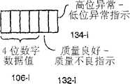
图2C说明了本发明一相应实施例,其中一数据存储值102具有特定的16个电平,因而相关联的数字数据值106-i具有4个位。通过附加第5个位将质量指示132-i与此数字数据值相关联,表示“质量良好”或“质量不良”,且将异常指示134-i作为第6个位与之相关联,表示“高位异常”或“低位异常”。FIG. 2C illustrates a corresponding embodiment of the present invention in which a
可将数字数据值106-i读入控制器27,以使用错误校正码来处理,而相关联的质量指示可暂时存储于(例如)缓冲器中。以后如果错误校正码需要进一步的指示可读取此质量指示。Digital data values 106-i may be read into
可将质量指示与已在存储器中的数字数据值相关联。在上述实施例中,以7位精度读取数据存储值。接着将4位数字数据值106-i和质量指示132-i和134-i与存储器内的数据存储值102相关联且随后移出到控制器。A quality indication can be associated with a digital data value already in memory. In the above embodiments, data store values are read with 7-bit precision. The 4-bit digital data value 106-i and quality indications 132-i and 134-i are then associated with the
在其它实施例中,可将数据存储值的7位表示移出到控制器,且控制器抽取代表性的4位数字数据值和相关的质量指示。在进一步的实施例中,在上述实例中产生具有27=128个条目的“查找”表。这些条目在查找表中的地址对应于数据存储值可处于的128个子区间。在这些地址处的条目可含有6个位,4个表示数字数据值而剩下的2个表示质量指示。质量指示可显示(例如)“质量良好”或“质量不良”以及“高位异常”或“低位异常”。这些查找表可寄存于(例如)随机存取存储器中。当读取数据存储值时,确定数据存储值所处在的子区间。接着,将查找表的对应于所确定子区间的6位条目移出到控制器以供进一步处理。In other embodiments, the 7-bit representation of the data storage value may be shifted out to the controller, and the controller extracts the representative 4-bit digital data value and associated quality indication. In a further embodiment, a "lookup" table with 27 =128 entries is generated in the above example. The addresses of these entries in the lookup table correspond to the 128 subintervals in which data storage values can lie. Entries at these addresses may contain 6 bits, 4 representing the digital data value and the remaining 2 representing the quality indication. Quality indicators may show, for example, "good quality" or "bad quality" and "abnormal high" or "abnormal low". These look-up tables can be stored, for example, in random access memory. When reading a data store value, determine the subinterval in which the data store value is located. Then, the 6-bit entry of the lookup table corresponding to the determined subinterval is shifted out to the controller for further processing.
数字数据值106-i可因各种原因而遭到破坏。某些原因可能是从存储单元泄漏电荷,此问题由于高密度存储系统中的存储单元的尺寸不断减小而加剧。这些高密度也是通过减小单元间间隔而实现的。现代存储器阵列设计中的此方面使得在临近的存储单元间发生干扰的机会增大。例如,一个存储单元的电荷可产生电场,其一部分会影响并改变另一存储单元的读出电流。最后,数据还可取决于单元所经历的历史而遭到破坏。经过过多写入和读出的存储单元中的数据存储值更有可能由于偏移离开优选中心范围而产生错误。Digital data values 106-i can be corrupted for various reasons. Some of the causes may be charge leakage from memory cells, a problem exacerbated by the ever-decreasing size of memory cells in high-density memory systems. These high densities are also achieved by reducing the inter-cell spacing. This aspect of modern memory array design increases the chance of interference between adjacent memory cells. For example, the charge of one memory cell can generate an electric field, a portion of which affects and changes the read current of another memory cell. Finally, data can also be corrupted depending on the history experienced by the unit. Data storage values in memory cells that have undergone excessive writing and reading are more likely to be erroneous due to offsets away from the preferred center range.
因为可能有破坏,所以不应在没有某种形式的测试和校正的情况下将数字数据值传送给用户。在许多存储系统中,通过将错误校正码(ECC)应用于数字数据值106-i来执行这些功能。通常当将数据写入存储器时将ECC应用于数据,且结果存储于(例如)数据旁的额外的位中。一个例子是(7,4)汉明码,其将三个额外的位与每个四位字相关联,以在16个可能的四位数据中的任意2个之间实现3的最小汉明距离(minimum Hamming distance)。当读取相同数据及其相关ECC位时重新计算ECC,且可将重新计算ECC的结果与数学上预期的结果相比较。如果重新计算的结果与预期结果相同,则数据可能未遭破坏,但是,如果重新计算的结果与预期结果不一致,则数据已遭到破坏。Because of the possibility of corruption, digital data values should not be transmitted to the user without some form of testing and correction. In many storage systems, these functions are performed by applying error correction code (ECC) to the digital data values 106-i. Typically ECC is applied to data when it is written to memory, and the result is stored, for example, in an extra bit next to the data. An example is a (7,4) Hamming code, which associates three extra bits with each quartet to achieve a minimum Hamming distance of 3 between any 2 of the 16 possible quartets (minimum Hamming distance). The ECC is recalculated when the same data and its associated ECC bits are read, and the result of the recalculated ECC can be compared to the mathematically expected result. If the recalculated results are as expected, the data may not be corrupted, but if the recalculated results are not as expected, the data is corrupted.
值得一提的是可将ECC应用于不同大小的数据组。此外,在快速存储器系统中,可为ECC的相关数据区段计算ECC,而大体上同时地读取数据。It is worth mentioning that ECC can be applied to data sets of different sizes. Furthermore, in a fast memory system, the ECC can be calculated for the associated data sectors of the ECC while the data is read substantially simultaneously.
一旦遭破坏的数据项的数目超过由所用的特定ECC定义的临界值,正确重构数据的概率就急剧下降。例如,如果在512个字节数据的区段中1或2个数据项遭破坏,则适当的ECC可以100%的确定性重构遭破坏的数据。然而,如果遭破坏数据的数目高于一临界数,例如在3和10之间(对于某些ECC约为5),则ECC正确重构数据的概率极低,而潜在地不正确重构数据的概率极高。Once the number of corrupted data items exceeds a threshold defined by the particular ECC used, the probability of correctly reconstructing the data drops dramatically. For example, if 1 or 2 data items are corrupted in a sector of 512 bytes of data, proper ECC can reconstruct the corrupted data with 100% certainty. However, if the number of corrupted data is above a critical number, say between 3 and 10 (about 5 for some ECCs), then the ECC has a very low probability of correctly reconstructing the data, and potentially incorrectly reconstructing the data very high probability.
许多ECC将额外的位用于数据恢复。汉明(Hamming)首先给出了有关ECC重构数据能力的通用关系式。如果一存储系统使用长度为m的二进制字,能够编码n=2m个不同数据,则如果此存储系统使用至少P个额外的位,就能可靠地校正t个遭破坏的数据,其中“汉明下限(lower Hamming limit)”给出P值的下界:Many ECCs use extra bits for data recovery. Hamming (Hamming) first gave a general relational expression about the ability of ECC to reconstruct data. If a storage system is capable of encoding n = 2m different data using binary words of length m, then it can reliably correct t corrupted data if the storage system uses at least P extra bits, where "Han "lower Hamming limit" gives the lower bound on the P value:
等效地,可将此关系式解读为:如果存储系统使用P个额外的位,则ECC能够可靠地重构具有至多t个遭破坏位的字。在许多系统中,选取P使得可以高可靠性重构具有1或2个错误的数据区段。Equivalently, this relation can be read as: ECC is able to reliably reconstruct a word with at most t corrupted bits if the storage system uses P extra bits. In many systems, P is chosen such that data sectors with 1 or 2 errors can be reconstructed with high reliability.
为解决此问题,ECC不但产生对数据的最可能的重构,还评估重构而成的数据的可靠性。在上述实例中,如果ECC检测到有大约1或2个遭破坏数据。则ECC可指示重构而成的数据很可能是正确的。在此情况下,可将重构而成的数据从控制器27传送给用户。如果ECC发现大约3到5个遭破坏数据,则ECC可指示正确重构遭破坏数据的概率减小了。取决于数据的随后用途,控制器27可接着决定是否接受或拒绝重构而成的数据和是否将其传送给用户。最后,如果ECC发现约5个以上的遭破坏数据,则ECC可指示正确重构遭破坏数据的概率非常低或无法重构数据。在不同的ECC实施中,实际的数值可不同于所引用的数值。To solve this problem, ECC not only produces the most likely reconstruction of data, but also evaluates the reliability of the reconstructed data. In the example above, if the ECC detects that there is about 1 or 2 corrupted data. The ECC may then indicate that the reconstructed data is likely to be correct. In this case, the reconstructed data can be transmitted from the
亦可能重构出错误数据。由于ECC仅使用关于数据区段的概要指示,其也可能巧合地用表面上降低了错误计数的“3”替换遭破坏的“8”,并因而接受“3”。这种错误数据重构可迅速使数据恢复恶化,并使其不可靠。It is also possible to reconstruct wrong data. Since ECC only uses a summary indication about data sectors, it may also coincidentally replace the corrupted "8" with a "3" that apparently lowers the error count, and thus accept the "3". This incorrect data reconstruction can quickly degrade data recovery and make it unreliable.
在这些和其它可靠性减小的情况下,控制器27可采用辅助校正方法来增加ECC的可靠性。本发明的某些实施例通过提供关于数据的额外指示来增加ECC的可靠性。例如,可通过控制器27读入与数字数据值106-i相关联的所存储质量指示来实现此目的。In these and other reduced reliability situations,
ECC重构数据能力的限制的一个原因在于:ECC无法确定数据区段内的遭破坏位的位置,且因而无法校正遭破坏的数据。因为“质量不良”数据是遭破坏数据的可能候选,且因为当确定了数据项的质量时,其位置也为已知了,所以此问题可通过本发明的某些实施例加以补救。因此,也可将“质量不良”数据的位置提供到ECC。从而,通过向错误校正过程提示可能有错的位(基于其被识别为“质量不良”),可增强ECC在可用于校正错误的时间范围中可靠地重构数据的能力。One reason for the limitation of ECC's ability to reconstruct data is that ECC cannot determine the location of corrupted bits within a data sector, and thus cannot correct corrupted data. Because "bad quality" data is a likely candidate for corrupted data, and because when the quality of a data item is determined, its location is also known, this problem can be remedied by some embodiments of the present invention. Therefore, the location of "bad quality" data may also be provided to the ECC. Thus, by cueing potentially erroneous bits to the error correction process based on their identification as "bad quality", the ability of the ECC to reliably reconstruct data over the time frame available to correct errors can be enhanced.
图3说明了某些实施例的另一优点:这些实施例可为ECC提供有关如何重构遭破坏数据项的建议。例如,如果计算ECC指示出在一数据区段中有遭破坏的数据,则具有指示“质量不良”的质量指示器132-i的4位数字数据值106-i是遭破坏数据的可能候选。尤其地,如果4位数字数据值106-i具有“低位异常”指示,则有可能在遭破坏之前对应存储数据值102由低1的数字数据值106-(i-1)表示。例如,如果“质量不良”数据存储值的数字数据值是“8”并具有“低位异常”指示,则有可能在遭破坏之前存储数据值对应于数字数据值“7”并自此向上偏移了。此实施例可接着提示ECC尝试将遭破坏的“8”特定地校正到“7”。此建议可增加重构而成的数据的可靠性并因而增加ECC的效率,因为当没有此种指示时,ECC必须在校正遭破坏的“8”过程中尝试所有可能的数,从而降低了其在可用于校正数据的通常较短时间范围内正确重构遭破坏数据的概率。Figure 3 illustrates another advantage of certain embodiments: These embodiments can provide ECC with advice on how to reconstruct corrupted data items. For example, if computing the ECC indicates that there is corrupted data in a sector of data, then a 4-bit numeric data value 106-i having a quality indicator 132-i indicating "bad quality" is a likely candidate for corrupted data. In particular, if the 4-bit digital data value 106-i has a "low bit exception" indication, it is possible that the corresponding stored
有可能在读取一区段时多个数字数据值被定性为“质量不良”。如果“质量不良”数字数据值的数目为n,则有2n-1种根据质量指示校正遭破坏数据的可能方式,因为n个数字数据值之每一个都可被个别地改变。在这2n-1种可能的校正当中可以高的概率找到重构成的数据。因而,通过向ECC提示以首先尝试这2n-1种组合来开始数据重构,可能更快地重构数字数据值。值得一提的是无需额外的费时的读取操作,ECC和控制器已可利用用于数据重构的所有指示。It is possible that multiple digital data values are characterized as "bad quality" when reading a sector. If the number of "bad quality" digital data values is n, there are2n -1 possible ways of correcting the corrupted data according to the quality indication, since each of the n digital data values can be changed individually. The reconstructed data can be found with high probability among these2n -1 possible corrections. Thus, it is possible to reconstruct digital data values faster by hinting to the ECC to start data reconstruction by first trying these2n -1 combinations. It is worth mentioning that the ECC and the controller already have all the indications for data reconstruction available without additional time-consuming read operations.
可以另一种方式利用质量指示。当从存储系统读取一区段的数据时,也可收集质量指示以产生并跟踪此区段的数据存储值的统计分布和其质量。这样做的优点在于数据破坏在某些区段中可为系统性的。此之原因的根源可在于外部环境,诸如温度改变、更改了区段的操作参数。或者,原因可与区段的历史有关联。例如,因为删除操作(基于Fowler-Nordheim隧道效应)可将某些闪存单元的源极-基板结(source-substrate junction)偏压到接近击穿电压,频繁的删除操作可造成存储单元的物理结构恶化,可能导致电荷损耗。而且,因为制造或材料不规则性,有可能在制造过程期间特定区段的特性偏离于优选值。可通过使用质量指示的统计资料来校正这种系统性数据破坏。Quality indicators can be utilized in another way. When a segment of data is read from the storage system, quality indicators may also be collected to generate and track the statistical distribution of the segment's data storage values and their quality. The advantage of this is that data corruption can be systemic in certain sectors. The root cause of this may lie in the external environment, such as a temperature change, changing the operating parameters of the section. Alternatively, the reason may be associated with the segment's history. For example, because erase operations (based on Fowler-Nordheim tunneling) can bias the source-substrate junction of some flash memory cells close to the breakdown voltage, frequent erase operations can cause damage to the memory cell's physical structure. deterioration, which may result in charge loss. Furthermore, it is possible that the properties of a particular segment deviate from preferred values during the manufacturing process because of manufacturing or material irregularities. This systematic data corruption can be corrected by using quality-indicating statistics.
图4A-C说明在两个相邻存储值区间104-i和104-(i+1)中的数据存储值的可能统计分布。如图4A中所示,在典型情况下,数据存储值将表现出呈122-i和122-(i+1)类型的在对应的优选中心范围108-i和108-(i+1)周围的分布。在此情况下,分布122-i和122-(i+1)是截然分开的,其意为:多数或所有数据存储值处于接近对应优选中心范围108-i和108-(i+1)处,且很少或无数据存储值处于分离点127-i附近。可通过在分布122-I与122-(i+1)之间引入分离间隙129-i的概念来重新表达此事实。分离间隙129-i表示其中很少有或无数据存储值存在的范围,且其位于分离点127-i周围。将把处于分离点127-i与127-(i+1)之间的数据存储值与数字数据值106-i相关联等等。4A-C illustrate possible statistical distributions of data storage values in two adjacent storage value intervals 104-i and 104-(i+1). As shown in FIG. 4A , in typical cases, the data storage values will exhibit 122-i and 122-(i+1) types around corresponding preferred center ranges 108-i and 108-(i+1). Distribution. In this case, the distributions 122-i and 122-(i+1) are distinct, which means that most or all of the data storage values lie near the corresponding preferred central ranges 108-i and 108-(i+1) , and few or no data storage values are near the separation point 127-i. This fact can be re-expressed by introducing the concept of separation gap 129-i between distributions 122-1 and 122-(i+1). Separation gap 129-i represents a range in which little or no data storage values exist and is located around separation point 127-i. The data storage values between split points 127-i and 127-(i+1) will be associated with digital data values 106-i and so on.
图4A展示一实施例,其中存储值区间104-i和104-(i+1)被分别划分为子区间116-i-j和116-(i+1)-j,其中j可取1与7之间的值。在此实施例中,分布是截然分开,如果多数或所有数据存储值处于j值在2与6之间的子区间中,则这些数据存储值中的大多数处于j值在3与5之间的中心优选范围中。在此种分布截然分开的情况下,将数据存储值102与数字数据值106-i相关联可具有高可靠性。FIG. 4A shows an embodiment in which the stored value intervals 104-i and 104-(i+1) are divided into sub-intervals 116-i-j and 116-(i+1)-j, respectively, where j can be between 1 and 7 value. In this example, the distributions are sharply split such that if most or all of the datastore values are in a subinterval with values of j between 2 and 6, then a majority of those datastore values are between values of j between 3 and 5 in the preferred range of the center. Where such distributions are sharply separated, there may be high reliability in associating data storage values 102 with digital data values 106-i.
图4B展示了一种可能的情形,其中相邻分布122-i和122-(i+1)以系统的方式遭到破坏。此系统的破坏可由(例如)温度变化造成。在此情况下,分布122-i和122-(i+1)向上偏移,其意为:“高位异常”数据的数目大于“低位异常”数据的数目。在此系统偏移的情况下,分布122-i、122-(i+1)和122-(i+2)仍保持截然分开。Figure 4B illustrates a possible situation where the adjacent distributions 122-i and 122-(i+1) are corrupted in a systematic manner. Disruption of this system can be caused by, for example, temperature changes. In this case, the distributions 122-i and 122-(i+1) are upwardly shifted, which means that the number of "high anomaly" data is greater than the number of "low anomaly" data. With this systematic shift, the distributions 122-i, 122-(i+1) and 122-(i+2) remain sharply separated.
图4B再次说明了一实施例,其中存储值区间104-i被进一步划分为子区间116-i-j。通过分布122-i、122-(i+1)和122-(i+2)在j=1的子区间内有一些数据存储值,在j=2、3和4的子区间内大体上无数据存储值,且数据存储值的主体在j=5、6和7的子区间内可看出系统偏移。在此情况下,在被偏移之前,子区间116-(i+1)-1中的数据存储值很可能对应于存储值区间104-i且因而与数字数据值106-i相关联,而不是与106-(i+1)相关联(在未修正过程中其会与这些数据存储值相关联)。Figure 4B again illustrates an embodiment in which the interval of stored values 104-i is further divided into sub-intervals 116-i-j. By distributions 122-i, 122-(i+1) and 122-(i+2) there are some data storage values in the subinterval of j=1 and substantially none in the subintervals of j=2, 3 and 4 The data store values, and the body of data store values in the j=5, 6 and 7 subintervals see a systematic shift. In this case, before being shifted, the data storage values in subinterval 116-(i+1)-1 likely correspond to storage value interval 104-i and are thus associated with digital data values 106-i, whereas Not associated with 106-(i+1) (which would be associated with these data store values in the uncorrected process).
如果发现一区段的数据存储值的统计资料表现出系统偏移且分布以偏移的分离间隙129-i′保持截然分开,则在某些实施例中,在收集了充分的关于数据区段的统计资料后,控制器27可采用某些校正行为。对于每一对相邻分布122-i和122-(i+1),控制器27可识别这些分布的相应系统偏移,且接着将分离点127-i以识别出的系统偏移进行偏移,到127-i′。在图4B的实例中,分布122-i和122-(i+1)和特别是其分离间隙129-i已向上偏移了两个子区间。所以控制器27可通过将分离点127-i向上偏移两个子区间到127-i′来抵消此系统偏移。此意味着在随后的读取操作中,处于区间116-(i+1)-1中的数据存储值(显然属于分布122-i)将被指定正确的数字数据值106-i而非106-(i+1)。If the statistics of the data storage values for a segment are found to exhibit a systematic shift and are distributed with offset separation gaps 129-i' to remain sharply separated, then in some embodiments, after sufficient information about the data segment has been collected After obtaining the statistical data, the
这些偏移不需要在总存储值区间100上为一致的,因为系统偏移的上述外部或内部原因可能不同地影响总存储值区间100中的不同存储值区间104-i。These offsets need not be consistent across the total stored value interval 100, since the aforementioned external or internal causes of systematic offsets may affect different stored value intervals 104-i in the total stored value interval 100 differently.
图4C说明了另一种可能性,其中相邻分布122-i和122-(i+1)未表现出系统偏移,而是表现出增宽。如图4C所示,此增宽可导致各分布的末尾部分重叠。当数据存储值处于此重叠区域中且用指定的数字数据值计算ECC指示出错误时,可个别地修改数字数据值的指定。类似于图3的实施例,如果数据存储值处于重叠区域中(例如,在子区间116-i-7中),则将使数字数据值106-i以及“质量不良”指示和“高位异常”指示与其相关联。因此,如果ECC在数据区段中检测到有错误,则基于质量指示,某些实施例将提示ECC将此数据存储值的指定从数字数据值106-i校正到数字数据值106-(i+1)。Figure 4C illustrates another possibility, where the adjacent distributions 122-i and 122-(i+1) do not exhibit a systematic shift, but instead exhibit broadening. As shown in Figure 4C, this broadening can cause the ends of the distributions to partially overlap. The designation of digital data values may be individually modified when the data storage value is in this overlapping region and calculating the ECC with the designated digital data value indicates an error. Similar to the embodiment of FIG. 3, if the data storage value is in an overlapping region (e.g., in subinterval 116-i-7), then digital data value 106-i along with a "bad quality" indication and a "high exception" will be made The indication is associated with it. Thus, if the ECC detects an error in a data segment, based on the quality indication, some embodiments will prompt the ECC to correct the assignment of this data storage value from digital data value 106-i to digital data value 106-(i+ 1).
根据本发明的另一方面,可基于一区段的“质量不良”数据的统计资料执行额外的校正行为。这些校正行为可由存储系统外部的控制器来执行或在其它实施例中由存储系统内部的某种逻辑来执行。在下文中,将执行校正行为的单元称为“控制器”。可在存储系统的任何数据区段中计数“质量不良”数据的总数。此计数可(例如)在区段数据的某些或所有读取过程期间执行,或在目的仅为确定区段的数据质量的特定“内务处理”操作期间执行。在此实施例中,甚至不需要应用ECC指示出在数据区段中存在错误。即使ECC指示数据区段无错误,“质量不良”数据的数目增加也显示出区段中的数据质量正在降低。受此指示的推动,可适时地执行抢先(proactive)校正行为,从而防止实际错误的出现。According to another aspect of the invention, additional corrective actions may be performed based on statistics of "bad quality" data for a segment. These corrective actions may be performed by a controller external to the storage system or in other embodiments by some logic internal to the storage system. In the following, the unit that performs the corrective action is called "controller". The total number of "bad quality" data can be counted in any data segment of the storage system. This counting may be performed, for example, during some or all read processes of the segment's data, or during certain "housekeeping" operations whose sole purpose is to determine the data quality of the segment. In this embodiment, it is not even necessary to apply ECC to indicate that there is an error in the data sector. Even if the ECC indicates that a data segment is error-free, an increase in the number of "bad quality" data indicates that the data quality in the segment is degrading. Motivated by this indication, proactive corrective actions can be performed in a timely manner, thereby preventing actual errors from occurring.
图5说明了根据“质量不良”数据的计数值来操作存储系统的流程图。Figure 5 illustrates a flow chart for operating the storage system based on a count of "bad quality" data.
a)如果C,一区段的“质量不良”数据的计数值为零或小于第一预定值N1,C<N1,此指示此区段的数据质量未降低或仅降低了较低的可容许的程度。因此无需校正行为。a) If C, the count value of "bad quality" data of a section is zero or less than the first predetermined value N1 , C<N1 , this indicates that the data quality of this section has not been degraded or only lower tolerable extent. So no need to correct behavior.
b)如果C,一区段的“质量不良”数据的计数值在第一与第二预定值之间,N1≤C<N2,此指示此区段的数据质量降低了一定程度。因此应在某时刻将此区段的数据刷新、重写或转录到另一区段。但是,降低的程度较小使得产生实际错误的概率较低。因此,上述校正行为无需立刻执行,而可推迟到以后一合适的时间。例如,可在存储系统已结束执行读取命令且亦未执行任何其它较高优先级的作业时执行这些校正行为。b) If C, the count value of "bad quality" data for a section is between the first and second predetermined values, N1 ≤ C<N2 , this indicates that the data quality of this section has degraded to a certain extent. So at some point the data of this segment should be flushed, rewritten or transcribed to another segment. However, the reduction is less so that the probability of actual error is lower. Therefore, the above-mentioned corrective action does not need to be performed immediately, but can be postponed to an appropriate time in the future. For example, these corrective actions may be performed when the storage system has finished executing a read command and is not executing any other higher priority jobs.
c)如果C,一区段的“质量不良”数据的计数值在第二与第三预定值之间,N2≤C<N3,此指示此区段的数据质量降低了相当大程度,此要求立即或在短暂的预定延迟时间内刷新、重写或转录此区段的数据。c) If C, the count of "bad quality" data for a section is between the second and third predetermined values, N2 ≤ C<N3 , this indicates that the data quality of this section has degraded considerably, This request flushes, rewrites, or transcribes the data for this segment immediately or within a short predetermined delay.
d)如果C,一区段的“质量不良”数据的计数值高于第三预定值,N3≤C,此指示此区段的数据质量降低到了不可容许的程度。降低的原因可能在区段内部,诸如,由过多读出和写入操作造成的广泛磨损、或某种材料或制造不规则性。在任一情况下,在未来写入此区段的数据质量也可能会降低。可通过立即或以高优先级将数据从此低质量区段转录到存储系统的另一区段来防止这种可预见的降低。接着可报废此低质量区段,使得在未来不会将数据写入其中。d) If C, the count of "bad quality" data for a section is higher than a third predetermined value, N3 ≦C, this indicates that the data quality of this section has degraded to an unacceptable level. The reason for the degradation may be within the sector, such as extensive wear from too many read and write operations, or some material or manufacturing irregularity. In either case, data written to this segment in the future may also be of reduced quality. This predictable degradation can be prevented by transcribing data from this low-quality segment to another segment of the storage system immediately or with high priority. This low quality segment can then be retired so that no data will be written to it in the future.
某些另外的实施例利用位于存储系统的常规存储单元间的跟踪单元。例如,在美国专利第6,222,762 B1号和第6,275,419 B1号(两案都颁予D.Guterman等人)中描述了跟踪单元及其操作。Certain additional embodiments utilize tracking units located between conventional storage units of the storage system. Tracking units and their operation are described, for example, in U.S. Patent Nos. 6,222,762 B1 and 6,275,419 B1 (both to D. Guterman et al.).
跟踪单元与常规存储单元经历相同的外部和内部影响,因而跟踪单元的统计资料可代表整个存储单元阵列的统计资料。因此,可依照图5中的步骤,仅根据跟踪单元中的“质量不良”数据的计数值来操作存储系统。Trace cells experience the same external and internal influences as conventional memory cells, so the statistics of the trace cells can be representative of the statistics of the entire array of memory cells. Therefore, the storage system can be operated according to the count value of "bad quality" data in the tracking unit only according to the steps in Fig. 5 .
另一实施例在读取一区段的数据时搜集了由ECC检测到的错误数。如图6中的流程图所示,可根据错误数执行不同类型的校正行为。Another embodiment collects the number of errors detected by ECC while reading a sector of data. As shown in the flowchart in Figure 6, different types of corrective actions can be performed depending on the number of errors.
a)如果E,一区段中的错误数为零或小于第一预定值M1,E<M1,此指示此区段的数据未遭破坏或仅以较低的可容许的程度遭到破坏,因此通过ECC(可能结合质量指示)其能可靠地重构。a) If E, the number of errors in a sector is zero or less than the first predetermined value M1 , E<M1 , this indicates that the data in this sector has not been corrupted or has only been corrupted to a lower tolerable degree Corruption, so it can be reliably reconstructed by ECC (possibly combined with quality indication).
b)如果E,一区段中的错误数在第一与第二预定值之间,M1≤E<M2,此指示此区段的数据已在一定程度上遭到破坏。因此,首先必须通过ECC(可能结合质量指示)重构此区段的数据,然后应在某时刻将此区段的数据刷新、重写或转录到另一区段。但是,破坏的程度较小使得仍可通过ECC(可结合质量指示)高度可靠地重构数据。此外,这些校正行为无需立刻执行,而可推迟到以后一合适的时间。例如,可在存储系统已结束执行读取命令且亦未执行任何其它较高优先级的作业时执行这些校正行为。b) If E, the number of errors in a sector is between the first and second predetermined values, M1 ≤ E<M2 , this indicates that the data in this sector has been corrupted to some extent. Therefore, first the data of this segment must be reconstructed by ECC (possibly combined with quality indication), and then at some point the data of this segment should be flushed, rewritten or transcribed to another segment. However, the degree of corruption is so small that the data can still be reconstructed with high reliability by ECC (Combinable Quality Indication). Furthermore, these corrective actions need not be performed immediately, but can be postponed until a suitable time later. For example, these corrective actions may be performed when the storage system has finished executing a read command and is not executing any other higher priority jobs.
c)如果E,一区段中的错误数在第二与第三预定值之间,M2≤E<M3,此指示此区段的数据已在相当大程度上遭到破坏。因此,首先必须通过ECC(可能结合质量指示)重构此区段的数据,然后应立即或在短暂的预定延迟时间内将此区段的数据刷新、重写或转录到另一新区段。c) If E, the number of errors in a sector is between the second and third predetermined values, M2 ≦E<M3 , this indicates that the data in this sector has been corrupted to a considerable extent. Therefore, first the data of this segment must be reconstructed by ECC (possibly combined with quality indication), and then the data of this segment should be flushed, rewritten or transcribed to another new segment immediately or within a short predetermined delay time.
d)如果E,一区段中的错误数高于第三预定值,M3≤E,此指示此区段的数据已被破坏到了不可容许的程度。破坏的原因可能在区段内部,诸如,由过多读出和写入操作造成的广泛磨损、或某种材料或制造不规则性。在任一情况下,在未来写入此区段的数据可能会再次遭到破坏。因此,首先必须通过ECC(可能结合质量指示)重构此区段的数据。其次,可通过立即或以高优先级将数据从遭破坏区段转录到存储系统的另一新区段来防止在未来对数据的破坏。然后,可报废此遭破坏区段,使得在未来不会将数据写入其中。d) If E, the number of errors in a sector is higher than a third predetermined value, M3 ≦E, this indicates that the data in this sector has been corrupted to an unacceptable level. The cause of the damage may be inside the sector, such as extensive wear from too many read and write operations, or some material or manufacturing irregularity. In either case, data written to this extent in the future may be corrupted again. Therefore, first the data of this section must be reconstructed by ECC (possibly combined with quality indication). Second, future corruption of data can be prevented by transcribing data from a corrupted segment to another new segment of the storage system immediately or with high priority. This corrupted section can then be retired so that no data will be written to it in the future.
如先前提及,错误校正码无法以高概率恢复多于数目K的遭破坏数据。在前例中,K的值为5。如果在一区段中多于K个数据遭到破坏,有时将这种情况称为:ECC被“淹没(swamped)”。在以上流程图中,M3可等于或不同于K。具体来说,可如此操作存储系统,使得即使ECC可以高概率重构数据,即E<K,也将转录数据且报废此区段,即M3<E<K。As mentioned previously, error correcting codes cannot recover more than the number K of corrupted data with high probability. In the previous example, the value of K was 5. If more than K pieces of data are corrupted in a sector, this situation is sometimes referred to as: ECC being "swamped". In the above flowchart,M3 may be equal to or different from K. Specifically, the storage system can be operated such that even if ECC can reconstruct the data with high probability, ie, E<K, the data will be transcribed and the segment retired, ie,M3 <E<K.
在某些实施例中,可用性能有限的计数器来计数错误。一个实例可为:如果ECC可在每个区段有4个遭破坏数据的情况下可靠地重构数据,即K=4,则每个区段可有一个四值计数器(four-value counter)。如果由ECC指示的错误数超过4,即E>4,则错误计数器可提供“溢出”信号。在这种情况下,ECC可再次尝试重构遭破坏的数据,但现在还要通过利用质量指示。如果结果令人满意,则可接受其并随后传送给用户。In some embodiments, limited performance counters may be used to count errors. An example could be: If ECC can reliably reconstruct data with 4 corrupted data per sector, i.e. K=4, then each sector can have a four-value counter . If the number of errors indicated by ECC exceeds 4, ie E>4, the error counter may provide an "overflow" signal. In this case, ECC can try again to reconstruct the corrupted data, but now by utilizing the quality indication. If the result is satisfactory, it is accepted and then communicated to the user.
尽管已关于某些优选实施例描述了本发明的各个方面,但应了解本发明有资格在附加的权利要求的完整范畴内受到保护。While various aspects of the invention have been described with respect to certain preferred embodiments, it should be understood that the invention is entitled to protection within the full scope of the appended claims.
Claims (34)
- One kind the operation one storage system method, it comprises:From described storage system reading of data storing value and wrong correction data;Indicate by digital data value and relevant quality and to represent indivedual described data storage value through reading; WithThe indication of one error-correcting code and quality combined be applied to have represented the digital data value of the described data storage value that reads from described storage system.
- 2. the method for claim 1 is wherein carried out the described of described data storage value abreast from a plurality of non-volatile memory cells and is read.
- 3. the method for claim 1, represent that wherein described indivedual described data storage value through reading comprises:The non-overlapped storage value interval that is defined according to described data storage value is positioned produces digital data value, and wherein said non-overlapped storage value interval comprises a central preferred range and is adjacent to its at least one peripheral extent.
- 4. the method for claim 1, wherein indicate and represent that described indivedual described data storage value through reading comprises by relevant quality:Produce relevant quality indication, to indicate described data storage value to be in the preferable range of described storage value interval at its place or to be in the adjacent range of described storage value interval at its place, indicate the quality good data in the time of by this in described data storage value is in described preferable range, and indicate the quality bad data in described data storage value is in described adjacent range the time.
- 5. method as claimed in claim 4, wherein said storage value interval comprise central preferred range and abut against a peripheral extent of described each side of preferable range, and wherein produce described relevant quality indication in addition and comprise:Produce an indication, its indication described data storage value when the bad indication of a quality is associated with described data storage value is in which scope in the described peripheral extent.
- 6. method as claimed in claim 5 wherein produces an indication of having indicated described data storage value to be in which scope in the described peripheral extent and comprises:When described data storage value is in the described peripheral extent that is adjacent to described central preferred range from the top, indicate high-order abnormal data; WithWhen described data storage value is in the described peripheral extent that is adjacent to described central preferred range from the below, indication low level abnormal data.
- 7. method as claimed in claim 6, wherein indicate and represent that described data storage value comprises by digital data value and relevant quality:By relevant described digital data value, a numeral good by its relevant quality or the bad indication of quality is represented other described data storage value with a numeral of or high-order unusual indication unusual by its relevant low level.
- 8. method as claimed in claim 7 wherein is applied to described digital data value with an error-correcting code and comprises:When applied error-correcting code can at least one destroyed digital data value of reconstruct, come described at least one the destroyed digital data value of reconstruct by using described error-correcting code, described by this at least one destroyed digital data value is detected by described error-correcting code; WithWhen applied error-correcting code can not at least one destroyed digital data value of reconstruct, by described error-correcting code and described relevant quality indication combination being used for described at least one the destroyed digital data value of reconstruct, described by this at least one destroyed digital data value is detected by described error-correcting code.
- 9. method as claimed in claim 8, wherein at least one destroyed digital data value of reconstruct comprises: use a relevant bad indication of quality to revise at least one digital data value.
- 10. method as claimed in claim 9, wherein revise at least one digital data value and comprise:Revise at least one digital data value according to described relevant indication, should relevant indicate corresponding data storage value to be in which scope in the described peripheral extent, when indicating low level unusual, reduce described at least one digital data value when high-order described at least one digital data value of increase when unusual of indication by this.
- 11. method as claimed in claim 10 wherein combines application with described error-correcting code with described correlated quality indication and comprises:Revise at least one digital data value according to described correlated quality indication; WithRepeat to revise the behavior of at least one digital data value and can proofread and correct described digital data value up to described error-correcting code.
- 12. the method for operation one storage system, it comprises:Read the plurality of data storing value from described storage system;Indicate by digital data value and relevant quality and to represent indivedual described plurality of data storing values through reading;The statistical data of a plurality of quality indications that structure one is associated with described plurality of data storing value; WithUtilize the described statistical data of relevant quality indication to operate described storage system.
- 13. method as claimed in claim 12 is wherein carried out the described of described data storage value abreast from a plurality of non-volatile memory cells and is read.
- 14. method as claimed in claim 12 represents that wherein described indivedual described data storage value through reading comprises:The non-overlapped storage value interval that is defined that is positioned according to described data storage value produces digital data value, and wherein said non-overlapped storage value interval is separated by burble point; WithThe position that is in the described storage value interval according to described data storage value produces described relevant quality indication.
- 15. method as claimed in claim 14, the described statistical data that wherein utilizes a plurality of correlated qualities to indicate is operated described storage system and is comprised:Described statistical data according to a plurality of correlated quality indications is revised described burble point.
- 16. method as claimed in claim 15, a statistics data of wherein constructing a plurality of correlated quality indications comprises:Establishment is in the number of the data storage value in the single sub-range of storage value interval, and wherein said storage value interval comprises a plurality of non-overlapped sub-ranges; WithThe identification Separation is as described one or more sub-ranges, and wherein the number of data storage value is less than a predetermined value.
- 17. method as claimed in claim 16 is wherein revised described burble point according to the described statistical data of described a plurality of correlated quality indications and is comprised:Revise at least one burble point, it is in the corresponding Separation.
- 18. the method for operation one storage system, it comprises:From described storage system reading of data storing value;Indicate by digital data value and correlated quality and to represent indivedual described data storage value through reading;The quality that is associated with the described data storage value of the plurality of memory cells indication of classification accumulation; WithDescribed storage system is operated in the described classification that utilization is indicated the quality that is accumulated.
- 19. method as claimed in claim 18 is wherein carried out the described of described data storage value abreast from non-volatile memory cells and is read.
- 20. method as claimed in claim 18 represents that wherein described indivedual described data storage value through reading comprises:The non-overlapped storage value interval that is defined that is positioned according to described data storage value produces digital data value, and wherein said non-overlapped storage value interval comprises a central preferred range and is adjacent to its at least one peripheral extent; WithProduce relevant quality indication, indicating described data storage value to be in the described preferable range or described adjacent range of storage value interval at its place, indication quality good data in the time of by this in described data storage value is in described preferable range and indicate the quality bad data when described data storage value is in described adjacent range in the time.
- 21. method as claimed in claim 20, the described quality indication that is associated with plurality of memory cells of wherein classifying comprises:The number of the quality bad data of establishment at least one plurality of memory cells.
- 22. method as claimed in claim 21 is wherein utilized the described classification that the quality that is accumulated is indicated to operate described storage system and is comprised:Manage the described data storage value of described at least one plurality of memory cells according to the number of the quality bad data of described plurality of memory cells, it comprises:When the number of quality bad data during, do not change described data storage value less than one first predetermined value.
- 23. method as claimed in claim 22 is wherein utilized and described storage system is operated in the described classification of the quality that accumulated indication is comprised one of following:Described data storage value is re-writed identical plurality of memory cells; WithWhen the number of quality bad data but when being not less than described first predetermined value,, after selected moment described data storage value is transcribed into a different plurality of memory cells according to the priority of system one less than one second predetermined value.
- 24. method as claimed in claim 23 is wherein utilized and described storage system is operated in the described classification of the quality that accumulated indication is comprised one of following:Described data storage value is re-writed described identical plurality of memory cells; WithWhen the number of quality bad data but when being not less than described second predetermined value, immediately or behind a predetermined delay, described data storage value is transcribed into a different plurality of memory cells less than one the 3rd predetermined value.
- 25. method as claimed in claim 24 is wherein utilized the described classification that the quality that is accumulated is indicated to operate described storage system and is comprised:The described data storage value of described at least one plurality of memory cells is transcribed into a different plurality of memory cells; WithWhen the number of quality bad data during, scrap described at least one plurality of memory cells less than one the 3rd predetermined value.
- 26. the method for operation one storage system, it comprises:From described storage system reading of data storing value;Indicate by digital data value and correlated quality and to represent indivedual described data storage value through reading;Use the number of an error-correcting code with the digital data value of the data storage value of judging destroyed expression plurality of memory cells;By being combined, described error-correcting code and the indication of described quality should be used for the described destroyed digital data value of reconstruct; WithUtilize the number of destroyed digital data value to operate described storage system.
- 27. method as claimed in claim 26 represents that wherein described indivedual described data storage value through reading comprises:The non-overlapped storage value interval that is defined that is positioned according to described data storage value produces digital data value, and wherein said non-overlapped storage value interval comprises a central preferred range and is adjacent to its at least one peripheral extent; WithProduce relevant quality indication, indicating described data storage value to be in the described preferable range or described adjacent range of storage value interval at its place, indication quality good data in the time of by this in described data storage value is in described preferable range and indicate the quality bad data when described data storage value is in described adjacent range in the time.
- 28. method as claimed in claim 27, wherein said non-overlapped storage value interval comprise described central preferred range and a peripheral extent that abuts against described each side of preferable range, and wherein produce in addition described relevant quality indication and comprise:Produce an indication, its indication described data storage value when the bad indication of a quality is associated with described data storage value is in which scope in the described peripheral extent.
- 29. method as claimed in claim 28 wherein produces an indication of having indicated described data storage value to be in which scope in the described peripheral extent and comprises:When described data storage value is in the described peripheral extent that is adjacent to described central preferred range from the top, indicate high-order abnormal data; WithWhen described data storage value is in the described peripheral extent that is adjacent to described central preferred range from the below, indication low level abnormal data.
- 30. method as claimed in claim 29 is wherein indicated by digital data value and relevant quality and is represented that described indivedual described data storage value through reading comprises:By relevant described digital data value, a numeral good by its relevant quality or the bad indication of quality is represented described indivedual described data storage value through reading with a numeral of or high-order unusual indication unusual by its relevant low level.
- 31. method as claimed in claim 30 is wherein utilized the number of destroyed digital data value to operate described storage system and is comprised:Manage the described data storage value of described plurality of memory cells according to the number of the destroyed digital data value of described plurality of memory cells, it comprises:When the number of destroyed digital data value during, indicate the described data storage value of reconstruct in conjunction with described quality by described error-correcting code less than one first predetermined value.
- 32. method as claimed in claim 31 is wherein utilized the number of destroyed digital data value to operate described storage system and is comprised:Indicate the described data storage value of reconstruct by described error-correcting code in conjunction with described quality; With carry out one of following:Described data storage value is re-writed identical plurality of memory cells; WithWhen the number of destroyed digital data value but when being not less than described first predetermined value, described data storage value is transcribed into a different plurality of memory cells after selected moment according to the priority of system one less than one second predetermined value.
- 33. method as claimed in claim 32 is wherein utilized the number of destroyed digital data value to operate described storage system and is comprised:Indicate the described data storage value of reconstruct by described error-correcting code in conjunction with described quality; With carry out one of following:Described data storage value is re-writed described identical plurality of memory cells; WithWhen the number of destroyed digital data value less than one the 3rd predetermined value but when being not less than described second predetermined value, immediately or behind a predetermined delay described data storage value is transcribed into a different plurality of memory cells.
- 34. method as claimed in claim 33 is wherein utilized the number of destroyed digital data value to operate described storage system and is comprised:Indicate the described data storage value of reconstruct by described error-correcting code in conjunction with described quality;Described data storage value is transcribed into a different plurality of memory cells; WithWhen the number of destroyed digital data value is not less than one the 3rd predetermined value, scrap described plurality of memory cells.
Applications Claiming Priority (2)
| Application Number | Priority Date | Filing Date | Title |
|---|---|---|---|
| US10/152,137US6751766B2 (en) | 2002-05-20 | 2002-05-20 | Increasing the effectiveness of error correction codes and operating multi-level memory systems by using information about the quality of the stored data |
| US10/152,137 | 2002-05-20 |
Publications (2)
| Publication Number | Publication Date |
|---|---|
| CN1653554A CN1653554A (en) | 2005-08-10 |
| CN100576359Ctrue CN100576359C (en) | 2009-12-30 |
Family
ID=29419533
Family Applications (1)
| Application Number | Title | Priority Date | Filing Date |
|---|---|---|---|
| CN03811328AExpired - LifetimeCN100576359C (en) | 2002-05-20 | 2003-05-12 | Increasing the efficiency of error-correcting codes and operating multi-level storage systems by using information about the quality of stored data |
Country Status (8)
| Country | Link |
|---|---|
| US (3) | US6751766B2 (en) |
| EP (1) | EP1506552B8 (en) |
| JP (1) | JP4638224B2 (en) |
| KR (1) | KR100993493B1 (en) |
| CN (1) | CN100576359C (en) |
| AU (1) | AU2003241428A1 (en) |
| TW (1) | TWI277099B (en) |
| WO (1) | WO2003100791A1 (en) |
Families Citing this family (290)
| Publication number | Priority date | Publication date | Assignee | Title |
|---|---|---|---|---|
| US6751766B2 (en)* | 2002-05-20 | 2004-06-15 | Sandisk Corporation | Increasing the effectiveness of error correction codes and operating multi-level memory systems by using information about the quality of the stored data |
| US6963505B2 (en)* | 2002-10-29 | 2005-11-08 | Aifun Semiconductors Ltd. | Method circuit and system for determining a reference voltage |
| US7237074B2 (en)* | 2003-06-13 | 2007-06-26 | Sandisk Corporation | Tracking cells for a memory system |
| US7372731B2 (en)* | 2003-06-17 | 2008-05-13 | Sandisk Il Ltd. | Flash memories with adaptive reference voltages |
| EP1654736B1 (en)* | 2003-07-30 | 2009-09-16 | SanDisk IL Ltd. | Method and system for optimizing reliability and performance of programming data in non-volatile memory devices |
| US7957189B2 (en)* | 2004-07-26 | 2011-06-07 | Sandisk Il Ltd. | Drift compensation in a flash memory |
| US7817469B2 (en)* | 2004-07-26 | 2010-10-19 | Sandisk Il Ltd. | Drift compensation in a flash memory |
| US7509526B2 (en)* | 2004-09-24 | 2009-03-24 | Seiko Epson Corporation | Method of correcting NAND memory blocks and to a printing device employing the method |
| WO2006051455A1 (en)* | 2004-11-09 | 2006-05-18 | Koninklijke Philips Electronics N.V. | Memory integrated circuit |
| US7404133B2 (en)* | 2004-12-12 | 2008-07-22 | Hewlett-Packard Development Company, L.P. | Error detection and correction employing modulation symbols satisfying predetermined criteria |
| JP4825874B2 (en)* | 2005-10-17 | 2011-11-30 | ラマト アット テル アビブ ユニバーシティ リミテッド | Probability-based error correction in multi-bit per-cell flash memory |
| US7526715B2 (en)* | 2005-10-17 | 2009-04-28 | Ramot At Tel Aviv University Ltd. | Probabilistic error correction in multi-bit-per-cell flash memory |
| US7954037B2 (en)* | 2005-10-25 | 2011-05-31 | Sandisk Il Ltd | Method for recovering from errors in flash memory |
| US7536627B2 (en)* | 2005-12-27 | 2009-05-19 | Sandisk Corporation | Storing downloadable firmware on bulk media |
| US7546515B2 (en)* | 2005-12-27 | 2009-06-09 | Sandisk Corporation | Method of storing downloadable firmware on bulk media |
| US8055979B2 (en)* | 2006-01-20 | 2011-11-08 | Marvell World Trade Ltd. | Flash memory with coding and signal processing |
| US7844879B2 (en)* | 2006-01-20 | 2010-11-30 | Marvell World Trade Ltd. | Method and system for error correction in flash memory |
| US7502254B2 (en)* | 2006-04-11 | 2009-03-10 | Sandisk Il Ltd | Method for generating soft bits in flash memories |
| WO2007132452A2 (en) | 2006-05-12 | 2007-11-22 | Anobit Technologies | Reducing programming error in memory devices |
| CN101512661B (en)* | 2006-05-12 | 2013-04-24 | 苹果公司 | Combined distortion estimation and error correction coding for memory devices |
| WO2007132453A2 (en)* | 2006-05-12 | 2007-11-22 | Anobit Technologies Ltd. | Distortion estimation and cancellation in memory devices |
| WO2007132456A2 (en) | 2006-05-12 | 2007-11-22 | Anobit Technologies Ltd. | Memory device with adaptive capacity |
| KR101202537B1 (en) | 2006-05-12 | 2012-11-19 | 애플 인크. | Combined distortion estimation and error correction coding for memory devices |
| US7852690B2 (en)* | 2006-05-15 | 2010-12-14 | Apple Inc. | Multi-chip package for a flash memory |
| US7639531B2 (en)* | 2006-05-15 | 2009-12-29 | Apple Inc. | Dynamic cell bit resolution |
| US7613043B2 (en)* | 2006-05-15 | 2009-11-03 | Apple Inc. | Shifting reference values to account for voltage sag |
| US7551486B2 (en) | 2006-05-15 | 2009-06-23 | Apple Inc. | Iterative memory cell charging based on reference cell value |
| US7511646B2 (en) | 2006-05-15 | 2009-03-31 | Apple Inc. | Use of 8-bit or higher A/D for NAND cell value |
| US8000134B2 (en) | 2006-05-15 | 2011-08-16 | Apple Inc. | Off-die charge pump that supplies multiple flash devices |
| US20070266296A1 (en)* | 2006-05-15 | 2007-11-15 | Conley Kevin M | Nonvolatile Memory with Convolutional Coding |
| US7911834B2 (en)* | 2006-05-15 | 2011-03-22 | Apple Inc. | Analog interface for a flash memory die |
| US7568135B2 (en)* | 2006-05-15 | 2009-07-28 | Apple Inc. | Use of alternative value in cell detection |
| US7639542B2 (en)* | 2006-05-15 | 2009-12-29 | Apple Inc. | Maintenance operations for multi-level data storage cells |
| US7840875B2 (en)* | 2006-05-15 | 2010-11-23 | Sandisk Corporation | Convolutional coding methods for nonvolatile memory |
| US7701797B2 (en)* | 2006-05-15 | 2010-04-20 | Apple Inc. | Two levels of voltage regulation supplied for logic and data programming voltage of a memory device |
| EP2052389A4 (en)* | 2006-08-05 | 2009-08-19 | Benhov Gmbh Llc | Solid state storage element and method |
| WO2008026203A2 (en)* | 2006-08-27 | 2008-03-06 | Anobit Technologies | Estimation of non-linear distortion in memory devices |
| US20080082725A1 (en)* | 2006-09-28 | 2008-04-03 | Reuven Elhamias | End of Life Recovery and Resizing of Memory Cards |
| US20080092015A1 (en)* | 2006-09-28 | 2008-04-17 | Yigal Brandman | Nonvolatile memory with adaptive operation |
| TWI360126B (en)* | 2006-09-28 | 2012-03-11 | Sandisk Corp | Nonvolatile memory with adaptive operations and me |
| US7904783B2 (en) | 2006-09-28 | 2011-03-08 | Sandisk Corporation | Soft-input soft-output decoder for nonvolatile memory |
| US7818653B2 (en) | 2006-09-28 | 2010-10-19 | Sandisk Corporation | Methods of soft-input soft-output decoding for nonvolatile memory |
| EP2069939B1 (en) | 2006-09-28 | 2013-01-02 | SanDisk Technologies Inc. | End of life recovery and resizing of memory cards |
| US7596656B2 (en)* | 2006-09-28 | 2009-09-29 | Sandisk Corporation | Memory cards with end of life recovery and resizing |
| US7805663B2 (en)* | 2006-09-28 | 2010-09-28 | Sandisk Corporation | Methods of adapting operation of nonvolatile memory |
| US8171380B2 (en) | 2006-10-10 | 2012-05-01 | Marvell World Trade Ltd. | Adaptive systems and methods for storing and retrieving data to and from memory cells |
| US7975192B2 (en) | 2006-10-30 | 2011-07-05 | Anobit Technologies Ltd. | Reading memory cells using multiple thresholds |
| WO2008053473A2 (en) | 2006-10-30 | 2008-05-08 | Anobit Technologies Ltd. | Memory cell readout using successive approximation |
| US8001441B2 (en)* | 2006-11-03 | 2011-08-16 | Sandisk Technologies Inc. | Nonvolatile memory with modulated error correction coding |
| US7558109B2 (en)* | 2006-11-03 | 2009-07-07 | Sandisk Corporation | Nonvolatile memory with variable read threshold |
| US7904788B2 (en)* | 2006-11-03 | 2011-03-08 | Sandisk Corporation | Methods of varying read threshold voltage in nonvolatile memory |
| US7904780B2 (en)* | 2006-11-03 | 2011-03-08 | Sandisk Corporation | Methods of modulating error correction coding |
| US7440319B2 (en)* | 2006-11-27 | 2008-10-21 | Sandisk Corporation | Apparatus with segmented bitscan for verification of programming |
| US7545681B2 (en)* | 2006-11-27 | 2009-06-09 | Sandisk Corporation | Segmented bitscan for verification of programming |
| US7924648B2 (en) | 2006-11-28 | 2011-04-12 | Anobit Technologies Ltd. | Memory power and performance management |
| JP4575346B2 (en)* | 2006-11-30 | 2010-11-04 | 株式会社東芝 | Memory system |
| WO2008068747A2 (en) | 2006-12-03 | 2008-06-12 | Anobit Technologies Ltd. | Automatic defect management in memory devices |
| US7900102B2 (en) | 2006-12-17 | 2011-03-01 | Anobit Technologies Ltd. | High-speed programming of memory devices |
| US7593263B2 (en) | 2006-12-17 | 2009-09-22 | Anobit Technologies Ltd. | Memory device with reduced reading latency |
| US7814401B2 (en) | 2006-12-21 | 2010-10-12 | Ramot At Tel Aviv University Ltd. | Soft decoding of hard and soft bits read from a flash memory |
| US7652918B2 (en)* | 2006-12-28 | 2010-01-26 | Sandisk Corporation | Retention margin program verification |
| US7616499B2 (en)* | 2006-12-28 | 2009-11-10 | Sandisk Corporation | Retention margin program verification |
| WO2008083162A1 (en)* | 2006-12-28 | 2008-07-10 | Sandisk Corporation | Retention margin program verification |
| KR100845529B1 (en)* | 2007-01-03 | 2008-07-10 | 삼성전자주식회사 | IC controller of flash memory device and memory system including it |
| KR100842680B1 (en) | 2007-01-08 | 2008-07-01 | 삼성전자주식회사 | Error Correction Controller of Flash Memory Device and Memory System Including It |
| US8151166B2 (en) | 2007-01-24 | 2012-04-03 | Anobit Technologies Ltd. | Reduction of back pattern dependency effects in memory devices |
| US7751240B2 (en) | 2007-01-24 | 2010-07-06 | Anobit Technologies Ltd. | Memory device with negative thresholds |
| US7861139B2 (en)* | 2007-01-26 | 2010-12-28 | Micron Technology, Inc. | Programming management data for NAND memories |
| JP5661227B2 (en)* | 2007-02-07 | 2015-01-28 | 株式会社メガチップス | Memory controller |
| US8369141B2 (en) | 2007-03-12 | 2013-02-05 | Apple Inc. | Adaptive estimation of memory cell read thresholds |
| US7966546B2 (en)* | 2007-03-31 | 2011-06-21 | Sandisk Technologies Inc. | Non-volatile memory with soft bit data transmission for error correction control |
| US7975209B2 (en)* | 2007-03-31 | 2011-07-05 | Sandisk Technologies Inc. | Non-volatile memory with guided simulated annealing error correction control |
| US7966550B2 (en) | 2007-03-31 | 2011-06-21 | Sandisk Technologies Inc. | Soft bit data transmission for error correction control in non-volatile memory |
| US7971127B2 (en)* | 2007-03-31 | 2011-06-28 | Sandisk Technologies Inc. | Guided simulated annealing in non-volatile memory error correction control |
| WO2008121577A1 (en)* | 2007-03-31 | 2008-10-09 | Sandisk Corporation | Soft bit data transmission for error correction control in non-volatile memory |
| US8001320B2 (en) | 2007-04-22 | 2011-08-16 | Anobit Technologies Ltd. | Command interface for memory devices |
| US7903468B2 (en)* | 2007-04-23 | 2011-03-08 | Ramot At Telaviv University Ltd. | Adaptive dynamic reading of flash memories |
| US8234545B2 (en) | 2007-05-12 | 2012-07-31 | Apple Inc. | Data storage with incremental redundancy |
| WO2008139441A2 (en) | 2007-05-12 | 2008-11-20 | Anobit Technologies Ltd. | Memory device with internal signal processing unit |
| KR20080100750A (en)* | 2007-05-14 | 2008-11-19 | 삼성전자주식회사 | Data reading device and method |
| JP2008300020A (en)* | 2007-06-04 | 2008-12-11 | Toshiba Corp | Playback device |
| US8006166B2 (en)* | 2007-06-12 | 2011-08-23 | Micron Technology, Inc. | Programming error correction code into a solid state memory device with varying bits per cell |
| KR101411976B1 (en)* | 2007-07-09 | 2014-06-27 | 삼성전자주식회사 | Flash memory system and its error correction method |
| US7925936B1 (en) | 2007-07-13 | 2011-04-12 | Anobit Technologies Ltd. | Memory device with non-uniform programming levels |
| US8259497B2 (en) | 2007-08-06 | 2012-09-04 | Apple Inc. | Programming schemes for multi-level analog memory cells |
| US8174905B2 (en) | 2007-09-19 | 2012-05-08 | Anobit Technologies Ltd. | Programming orders for reducing distortion in arrays of multi-level analog memory cells |
| US8650352B2 (en) | 2007-09-20 | 2014-02-11 | Densbits Technologies Ltd. | Systems and methods for determining logical values of coupled flash memory cells |
| US8365040B2 (en) | 2007-09-20 | 2013-01-29 | Densbits Technologies Ltd. | Systems and methods for handling immediate data errors in flash memory |
| US7751237B2 (en)* | 2007-09-25 | 2010-07-06 | Sandisk Il, Ltd. | Post-facto correction for cross coupling in a flash memory |
| US7773413B2 (en) | 2007-10-08 | 2010-08-10 | Anobit Technologies Ltd. | Reliable data storage in analog memory cells in the presence of temperature variations |
| US8068360B2 (en) | 2007-10-19 | 2011-11-29 | Anobit Technologies Ltd. | Reading analog memory cells using built-in multi-threshold commands |
| US8000141B1 (en) | 2007-10-19 | 2011-08-16 | Anobit Technologies Ltd. | Compensation for voltage drifts in analog memory cells |
| US8527819B2 (en) | 2007-10-19 | 2013-09-03 | Apple Inc. | Data storage in analog memory cell arrays having erase failures |
| US8694715B2 (en) | 2007-10-22 | 2014-04-08 | Densbits Technologies Ltd. | Methods for adaptively programming flash memory devices and flash memory systems incorporating same |
| US8443242B2 (en) | 2007-10-25 | 2013-05-14 | Densbits Technologies Ltd. | Systems and methods for multiple coding rates in flash devices |
| US8270246B2 (en) | 2007-11-13 | 2012-09-18 | Apple Inc. | Optimized selection of memory chips in multi-chips memory devices |
| US8499229B2 (en) | 2007-11-21 | 2013-07-30 | Micro Technology, Inc. | Method and apparatus for reading data from flash memory |
| US8225181B2 (en) | 2007-11-30 | 2012-07-17 | Apple Inc. | Efficient re-read operations from memory devices |
| US8429492B2 (en)* | 2007-11-30 | 2013-04-23 | Marvell World Trade Ltd. | Error correcting code predication system and method |
| WO2009072105A2 (en) | 2007-12-05 | 2009-06-11 | Densbits Technologies Ltd. | A low power chien-search based bch/rs decoding system for flash memory, mobile communications devices and other applications |
| US8335977B2 (en) | 2007-12-05 | 2012-12-18 | Densbits Technologies Ltd. | Flash memory apparatus and methods using a plurality of decoding stages including optional use of concatenated BCH codes and/or designation of “first below” cells |
| US8321625B2 (en) | 2007-12-05 | 2012-11-27 | Densbits Technologies Ltd. | Flash memory device with physical cell value deterioration accommodation and methods useful in conjunction therewith |
| US8209588B2 (en) | 2007-12-12 | 2012-06-26 | Anobit Technologies Ltd. | Efficient interference cancellation in analog memory cell arrays |
| US8359516B2 (en) | 2007-12-12 | 2013-01-22 | Densbits Technologies Ltd. | Systems and methods for error correction and decoding on multi-level physical media |
| US8276051B2 (en) | 2007-12-12 | 2012-09-25 | Densbits Technologies Ltd. | Chien-search system employing a clock-gating scheme to save power for error correction decoder and other applications |
| US7561484B2 (en)* | 2007-12-13 | 2009-07-14 | Spansion Llc | Reference-free sampled sensing |
| US8456905B2 (en) | 2007-12-16 | 2013-06-04 | Apple Inc. | Efficient data storage in multi-plane memory devices |
| US8327246B2 (en) | 2007-12-18 | 2012-12-04 | Densbits Technologies Ltd. | Apparatus for coding at a plurality of rates in multi-level flash memory systems, and methods useful in conjunction therewith |
| US8085586B2 (en) | 2007-12-27 | 2011-12-27 | Anobit Technologies Ltd. | Wear level estimation in analog memory cells |
| EP2077559B1 (en)* | 2007-12-27 | 2012-11-07 | Hagiwara Solutions Co., Ltd. | Refresh method of a flash memory |
| JP2009158043A (en)* | 2007-12-27 | 2009-07-16 | Elpida Memory Inc | Semiconductor integrated circuit and unstable bit detection method of the same |
| KR101368694B1 (en) | 2008-01-22 | 2014-03-03 | 삼성전자주식회사 | Apparatus and method of memory programming |
| US8156398B2 (en) | 2008-02-05 | 2012-04-10 | Anobit Technologies Ltd. | Parameter estimation based on error correction code parity check equations |
| US7924587B2 (en) | 2008-02-21 | 2011-04-12 | Anobit Technologies Ltd. | Programming of analog memory cells using a single programming pulse per state transition |
| US7864573B2 (en) | 2008-02-24 | 2011-01-04 | Anobit Technologies Ltd. | Programming analog memory cells for reduced variance after retention |
| US8230300B2 (en) | 2008-03-07 | 2012-07-24 | Apple Inc. | Efficient readout from analog memory cells using data compression |
| US8400858B2 (en) | 2008-03-18 | 2013-03-19 | Apple Inc. | Memory device with reduced sense time readout |
| US8059457B2 (en) | 2008-03-18 | 2011-11-15 | Anobit Technologies Ltd. | Memory device with multiple-accuracy read commands |
| WO2009118720A2 (en) | 2008-03-25 | 2009-10-01 | Densbits Technologies Ltd. | Apparatus and methods for hardware-efficient unbiased rounding |
| US8386868B2 (en)* | 2008-04-16 | 2013-02-26 | Sandisk Il, Ltd. | Using programming-time information to support error correction |
| KR101506655B1 (en) | 2008-05-15 | 2015-03-30 | 삼성전자주식회사 | How to Manage Memory Devices and Memory Data Errors |
| US8085591B2 (en) | 2008-05-20 | 2011-12-27 | Micron Technology, Inc. | Charge loss compensation during programming of a memory device |
| JP5292925B2 (en)* | 2008-05-30 | 2013-09-18 | 富士通株式会社 | Semiconductor integrated circuit, control method therefor, and information processing apparatus |
| US8321757B2 (en)* | 2008-06-22 | 2012-11-27 | Sandisk Il Ltd. | Method and apparatus for error correction |
| US7821839B2 (en)* | 2008-06-27 | 2010-10-26 | Sandisk Il Ltd. | Gain control for read operations in flash memory |
| US7808831B2 (en)* | 2008-06-30 | 2010-10-05 | Sandisk Corporation | Read disturb mitigation in non-volatile memory |
| US7924613B1 (en) | 2008-08-05 | 2011-04-12 | Anobit Technologies Ltd. | Data storage in analog memory cells with protection against programming interruption |
| US8498151B1 (en) | 2008-08-05 | 2013-07-30 | Apple Inc. | Data storage in analog memory cells using modified pass voltages |
| US8406048B2 (en) | 2008-08-08 | 2013-03-26 | Marvell World Trade Ltd. | Accessing memory using fractional reference voltages |
| US8332725B2 (en) | 2008-08-20 | 2012-12-11 | Densbits Technologies Ltd. | Reprogramming non volatile memory portions |
| US8213229B2 (en)* | 2008-08-22 | 2012-07-03 | HGST Netherlands, B.V. | Error control in a flash memory device |
| US8949684B1 (en) | 2008-09-02 | 2015-02-03 | Apple Inc. | Segmented data storage |
| US8169825B1 (en) | 2008-09-02 | 2012-05-01 | Anobit Technologies Ltd. | Reliable data storage in analog memory cells subjected to long retention periods |
| KR101483190B1 (en)* | 2008-09-05 | 2015-01-19 | 삼성전자주식회사 | Memory system and data processing method thereof |
| US8482978B1 (en) | 2008-09-14 | 2013-07-09 | Apple Inc. | Estimation of memory cell read thresholds by sampling inside programming level distribution intervals |
| US8000135B1 (en) | 2008-09-14 | 2011-08-16 | Anobit Technologies Ltd. | Estimation of memory cell read thresholds by sampling inside programming level distribution intervals |
| US8830748B2 (en) | 2008-09-30 | 2014-09-09 | Lsi Corporation | Methods and apparatus for soft data generation for memory devices |
| US8239734B1 (en) | 2008-10-15 | 2012-08-07 | Apple Inc. | Efficient data storage in storage device arrays |
| US8713330B1 (en) | 2008-10-30 | 2014-04-29 | Apple Inc. | Data scrambling in memory devices |
| KR101529880B1 (en)* | 2008-10-31 | 2015-06-19 | 삼성전자주식회사 | Error Estimation Method and Correction Method |
| US8407400B2 (en)* | 2008-11-12 | 2013-03-26 | Micron Technology, Inc. | Dynamic SLC/MLC blocks allocations for non-volatile memory |
| US8208304B2 (en) | 2008-11-16 | 2012-06-26 | Anobit Technologies Ltd. | Storage at M bits/cell density in N bits/cell analog memory cell devices, M>N |
| US8291297B2 (en)* | 2008-12-18 | 2012-10-16 | Intel Corporation | Data error recovery in non-volatile memory |
| US8174857B1 (en) | 2008-12-31 | 2012-05-08 | Anobit Technologies Ltd. | Efficient readout schemes for analog memory cell devices using multiple read threshold sets |
| US8248831B2 (en) | 2008-12-31 | 2012-08-21 | Apple Inc. | Rejuvenation of analog memory cells |
| US8924661B1 (en) | 2009-01-18 | 2014-12-30 | Apple Inc. | Memory system including a controller and processors associated with memory devices |
| US7894270B2 (en)* | 2009-02-11 | 2011-02-22 | Mosys, Inc. | Data restoration method for a non-volatile memory |
| US8161355B2 (en) | 2009-02-11 | 2012-04-17 | Mosys, Inc. | Automatic refresh for improving data retention and endurance characteristics of an embedded non-volatile memory in a standard CMOS logic process |
| US8228701B2 (en) | 2009-03-01 | 2012-07-24 | Apple Inc. | Selective activation of programming schemes in analog memory cell arrays |
| KR20100098969A (en) | 2009-03-02 | 2010-09-10 | 삼성전자주식회사 | Semiconductor device for improving reliability of error correction codes, semiconductor system having the same, and method for processing error correction code |
| US8458114B2 (en)* | 2009-03-02 | 2013-06-04 | Analog Devices, Inc. | Analog computation using numerical representations with uncertainty |
| US20100220514A1 (en)* | 2009-03-02 | 2010-09-02 | Lyric Semiconductor, Inc. | Storage devices with soft processing |
| US8832354B2 (en) | 2009-03-25 | 2014-09-09 | Apple Inc. | Use of host system resources by memory controller |
| US8259506B1 (en) | 2009-03-25 | 2012-09-04 | Apple Inc. | Database of memory read thresholds |
| US8107306B2 (en) | 2009-03-27 | 2012-01-31 | Analog Devices, Inc. | Storage devices with soft processing |
| US8819385B2 (en) | 2009-04-06 | 2014-08-26 | Densbits Technologies Ltd. | Device and method for managing a flash memory |
| US8458574B2 (en) | 2009-04-06 | 2013-06-04 | Densbits Technologies Ltd. | Compact chien-search based decoding apparatus and method |
| US8238157B1 (en) | 2009-04-12 | 2012-08-07 | Apple Inc. | Selective re-programming of analog memory cells |
| US8566510B2 (en) | 2009-05-12 | 2013-10-22 | Densbits Technologies Ltd. | Systems and method for flash memory management |
| FR2946787A1 (en)* | 2009-06-16 | 2010-12-17 | St Microelectronics Rousset | METHOD FOR DETECTING ATTACK BY FAULT INJECTION OF A MEMORY DEVICE, AND CORRESPONDING MEMORY DEVICE |
| US8255773B2 (en)* | 2009-06-29 | 2012-08-28 | Sandisk Technologies Inc. | System and method of tracking error data within a storage device |
| US8479080B1 (en) | 2009-07-12 | 2013-07-02 | Apple Inc. | Adaptive over-provisioning in memory systems |
| EP2299362A3 (en) | 2009-08-18 | 2011-05-04 | ViaSat, Inc. | Forward error correction for memories |
| US9330767B1 (en) | 2009-08-26 | 2016-05-03 | Avago Technologies General Ip (Singapore) Pte. Ltd. | Flash memory module and method for programming a page of flash memory cells |
| US8995197B1 (en) | 2009-08-26 | 2015-03-31 | Densbits Technologies Ltd. | System and methods for dynamic erase and program control for flash memory device memories |
| US8868821B2 (en) | 2009-08-26 | 2014-10-21 | Densbits Technologies Ltd. | Systems and methods for pre-equalization and code design for a flash memory |
| US8305812B2 (en) | 2009-08-26 | 2012-11-06 | Densbits Technologies Ltd. | Flash memory module and method for programming a page of flash memory cells |
| US8495465B1 (en) | 2009-10-15 | 2013-07-23 | Apple Inc. | Error correction coding over multiple memory pages |
| US8730729B2 (en) | 2009-10-15 | 2014-05-20 | Densbits Technologies Ltd. | Systems and methods for averaging error rates in non-volatile devices and storage systems |
| US8724387B2 (en) | 2009-10-22 | 2014-05-13 | Densbits Technologies Ltd. | Method, system, and computer readable medium for reading and programming flash memory cells using multiple bias voltages |
| US8510628B2 (en)* | 2009-11-12 | 2013-08-13 | Micron Technology, Inc. | Method and apparatuses for customizable error correction of memory |
| US8626988B2 (en) | 2009-11-19 | 2014-01-07 | Densbits Technologies Ltd. | System and method for uncoded bit error rate equalization via interleaving |
| US8677054B1 (en) | 2009-12-16 | 2014-03-18 | Apple Inc. | Memory management schemes for non-volatile memory devices |
| US9037777B2 (en) | 2009-12-22 | 2015-05-19 | Densbits Technologies Ltd. | Device, system, and method for reducing program/read disturb in flash arrays |
| US8607124B2 (en) | 2009-12-24 | 2013-12-10 | Densbits Technologies Ltd. | System and method for setting a flash memory cell read threshold |
| US8694814B1 (en) | 2010-01-10 | 2014-04-08 | Apple Inc. | Reuse of host hibernation storage space by memory controller |
| US8572311B1 (en) | 2010-01-11 | 2013-10-29 | Apple Inc. | Redundant data storage in multi-die memory systems |
| KR20120137354A (en) | 2010-01-28 | 2012-12-20 | 샌디스크 아이엘 엘티디 | Sliding-window error correction |
| US8341502B2 (en) | 2010-02-28 | 2012-12-25 | Densbits Technologies Ltd. | System and method for multi-dimensional decoding |
| US8516274B2 (en) | 2010-04-06 | 2013-08-20 | Densbits Technologies Ltd. | Method, system and medium for analog encryption in a flash memory |
| US8527840B2 (en) | 2010-04-06 | 2013-09-03 | Densbits Technologies Ltd. | System and method for restoring damaged data programmed on a flash device |
| US8745317B2 (en) | 2010-04-07 | 2014-06-03 | Densbits Technologies Ltd. | System and method for storing information in a multi-level cell memory |
| US20110252289A1 (en)* | 2010-04-08 | 2011-10-13 | Seagate Technology Llc | Adjusting storage device parameters based on reliability sensing |
| US9021177B2 (en) | 2010-04-29 | 2015-04-28 | Densbits Technologies Ltd. | System and method for allocating and using spare blocks in a flash memory |
| US8694853B1 (en) | 2010-05-04 | 2014-04-08 | Apple Inc. | Read commands for reading interfering memory cells |
| US8386895B2 (en) | 2010-05-19 | 2013-02-26 | Micron Technology, Inc. | Enhanced multilevel memory |
| US8572423B1 (en) | 2010-06-22 | 2013-10-29 | Apple Inc. | Reducing peak current in memory systems |
| US8468431B2 (en) | 2010-07-01 | 2013-06-18 | Densbits Technologies Ltd. | System and method for multi-dimensional encoding and decoding |
| US8539311B2 (en) | 2010-07-01 | 2013-09-17 | Densbits Technologies Ltd. | System and method for data recovery in multi-level cell memories |
| US20120008414A1 (en) | 2010-07-06 | 2012-01-12 | Michael Katz | Systems and methods for storing, retrieving, and adjusting read thresholds in flash memory storage system |
| US8595591B1 (en) | 2010-07-11 | 2013-11-26 | Apple Inc. | Interference-aware assignment of programming levels in analog memory cells |
| US9104580B1 (en) | 2010-07-27 | 2015-08-11 | Apple Inc. | Cache memory for hybrid disk drives |
| US8645794B1 (en) | 2010-07-31 | 2014-02-04 | Apple Inc. | Data storage in analog memory cells using a non-integer number of bits per cell |
| US8856475B1 (en) | 2010-08-01 | 2014-10-07 | Apple Inc. | Efficient selection of memory blocks for compaction |
| US8694854B1 (en) | 2010-08-17 | 2014-04-08 | Apple Inc. | Read threshold setting based on soft readout statistics |
| US8964464B2 (en) | 2010-08-24 | 2015-02-24 | Densbits Technologies Ltd. | System and method for accelerated sampling |
| US8508995B2 (en) | 2010-09-15 | 2013-08-13 | Densbits Technologies Ltd. | System and method for adjusting read voltage thresholds in memories |
| US9021181B1 (en) | 2010-09-27 | 2015-04-28 | Apple Inc. | Memory management for unifying memory cell conditions by using maximum time intervals |
| US9063878B2 (en) | 2010-11-03 | 2015-06-23 | Densbits Technologies Ltd. | Method, system and computer readable medium for copy back |
| US8850100B2 (en) | 2010-12-07 | 2014-09-30 | Densbits Technologies Ltd. | Interleaving codeword portions between multiple planes and/or dies of a flash memory device |
| US8498152B2 (en) | 2010-12-23 | 2013-07-30 | Sandisk Il Ltd. | Non-volatile memory and methods with soft-bit reads while reading hard bits with compensation for coupling |
| US8782495B2 (en)* | 2010-12-23 | 2014-07-15 | Sandisk Il Ltd | Non-volatile memory and methods with asymmetric soft read points around hard read points |
| US8099652B1 (en) | 2010-12-23 | 2012-01-17 | Sandisk Corporation | Non-volatile memory and methods with reading soft bits in non uniform schemes |
| US9292377B2 (en) | 2011-01-04 | 2016-03-22 | Seagate Technology Llc | Detection and decoding in flash memories using correlation of neighboring bits and probability based reliability values |
| US9898361B2 (en) | 2011-01-04 | 2018-02-20 | Seagate Technology Llc | Multi-tier detection and decoding in flash memories |
| US10079068B2 (en) | 2011-02-23 | 2018-09-18 | Avago Technologies General Ip (Singapore) Pte. Ltd. | Devices and method for wear estimation based memory management |
| US9502117B2 (en)* | 2011-03-14 | 2016-11-22 | Seagate Technology Llc | Cell-level statistics collection for detection and decoding in flash memories |
| US8693258B2 (en) | 2011-03-17 | 2014-04-08 | Densbits Technologies Ltd. | Obtaining soft information using a hard interface |
| US8990665B1 (en) | 2011-04-06 | 2015-03-24 | Densbits Technologies Ltd. | System, method and computer program product for joint search of a read threshold and soft decoding |
| US9110785B1 (en) | 2011-05-12 | 2015-08-18 | Densbits Technologies Ltd. | Ordered merge of data sectors that belong to memory space portions |
| US9195592B1 (en) | 2011-05-12 | 2015-11-24 | Densbits Technologies Ltd. | Advanced management of a non-volatile memory |
| US9501392B1 (en) | 2011-05-12 | 2016-11-22 | Avago Technologies General Ip (Singapore) Pte. Ltd. | Management of a non-volatile memory module |
| US9396106B2 (en) | 2011-05-12 | 2016-07-19 | Avago Technologies General Ip (Singapore) Pte. Ltd. | Advanced management of a non-volatile memory |
| US9372792B1 (en) | 2011-05-12 | 2016-06-21 | Avago Technologies General Ip (Singapore) Pte. Ltd. | Advanced management of a non-volatile memory |
| US8996790B1 (en) | 2011-05-12 | 2015-03-31 | Densbits Technologies Ltd. | System and method for flash memory management |
| US8667211B2 (en) | 2011-06-01 | 2014-03-04 | Densbits Technologies Ltd. | System and method for managing a non-volatile memory |
| US8775901B2 (en) | 2011-07-28 | 2014-07-08 | SanDisk Technologies, Inc. | Data recovery for defective word lines during programming of non-volatile memory arrays |
| US8750042B2 (en) | 2011-07-28 | 2014-06-10 | Sandisk Technologies Inc. | Combined simultaneous sensing of multiple wordlines in a post-write read (PWR) and detection of NAND failures |
| US8588003B1 (en) | 2011-08-01 | 2013-11-19 | Densbits Technologies Ltd. | System, method and computer program product for programming and for recovering from a power failure |
| US8553468B2 (en) | 2011-09-21 | 2013-10-08 | Densbits Technologies Ltd. | System and method for managing erase operations in a non-volatile memory |
| US8990644B2 (en) | 2011-12-22 | 2015-03-24 | Micron Technology, Inc. | Apparatus and methods of programming memory cells using adjustable charge state level(s) |
| US8947941B2 (en) | 2012-02-09 | 2015-02-03 | Densbits Technologies Ltd. | State responsive operations relating to flash memory cells |
| US8996788B2 (en) | 2012-02-09 | 2015-03-31 | Densbits Technologies Ltd. | Configurable flash interface |
| US8730722B2 (en) | 2012-03-02 | 2014-05-20 | Sandisk Technologies Inc. | Saving of data in cases of word-line to word-line short in memory arrays |
| US8996793B1 (en) | 2012-04-24 | 2015-03-31 | Densbits Technologies Ltd. | System, method and computer readable medium for generating soft information |
| US8793556B1 (en) | 2012-05-22 | 2014-07-29 | Pmc-Sierra, Inc. | Systems and methods for reclaiming flash blocks of a flash drive |
| US9176812B1 (en) | 2012-05-22 | 2015-11-03 | Pmc-Sierra, Inc. | Systems and methods for storing data in page stripes of a flash drive |
| US8788910B1 (en) | 2012-05-22 | 2014-07-22 | Pmc-Sierra, Inc. | Systems and methods for low latency, high reliability error correction in a flash drive |
| US8972824B1 (en)* | 2012-05-22 | 2015-03-03 | Pmc-Sierra, Inc. | Systems and methods for transparently varying error correction code strength in a flash drive |
| US8996957B1 (en) | 2012-05-22 | 2015-03-31 | Pmc-Sierra, Inc. | Systems and methods for initializing regions of a flash drive having diverse error correction coding (ECC) schemes |
| US9021337B1 (en) | 2012-05-22 | 2015-04-28 | Pmc-Sierra, Inc. | Systems and methods for adaptively selecting among different error correction coding schemes in a flash drive |
| US9183085B1 (en) | 2012-05-22 | 2015-11-10 | Pmc-Sierra, Inc. | Systems and methods for adaptively selecting from among a plurality of error correction coding schemes in a flash drive for robustness and low latency |
| US9021336B1 (en) | 2012-05-22 | 2015-04-28 | Pmc-Sierra, Inc. | Systems and methods for redundantly storing error correction codes in a flash drive with secondary parity information spread out across each page of a group of pages |
| US9021333B1 (en) | 2012-05-22 | 2015-04-28 | Pmc-Sierra, Inc. | Systems and methods for recovering data from failed portions of a flash drive |
| US8838937B1 (en) | 2012-05-23 | 2014-09-16 | Densbits Technologies Ltd. | Methods, systems and computer readable medium for writing and reading data |
| US8879325B1 (en) | 2012-05-30 | 2014-11-04 | Densbits Technologies Ltd. | System, method and computer program product for processing read threshold information and for reading a flash memory module |
| US9921954B1 (en) | 2012-08-27 | 2018-03-20 | Avago Technologies General Ip (Singapore) Pte. Ltd. | Method and system for split flash memory management between host and storage controller |
| US9299459B2 (en)* | 2012-09-07 | 2016-03-29 | Macronix International Co., Ltd. | Method and apparatus of measuring error correction data for memory |
| US20140071761A1 (en) | 2012-09-10 | 2014-03-13 | Sandisk Technologies Inc. | Non-volatile storage with joint hard bit and soft bit reading |
| US9368225B1 (en) | 2012-11-21 | 2016-06-14 | Avago Technologies General Ip (Singapore) Pte. Ltd. | Determining read thresholds based upon read error direction statistics |
| US20140181621A1 (en)* | 2012-12-26 | 2014-06-26 | Skymedi Corporation | Method of arranging data in a non-volatile memory and a memory control system thereof |
| US9069659B1 (en) | 2013-01-03 | 2015-06-30 | Densbits Technologies Ltd. | Read threshold determination using reference read threshold |
| US9070479B2 (en) | 2013-01-21 | 2015-06-30 | Sandisk Technologies Inc. | Systems and methods of updating read voltages |
| US8913428B2 (en)* | 2013-01-25 | 2014-12-16 | Sandisk Technologies Inc. | Programming non-volatile storage system with multiple memory die |
| US8861270B2 (en) | 2013-03-11 | 2014-10-14 | Microsoft Corporation | Approximate multi-level cell memory operations |
| US9009565B1 (en) | 2013-03-15 | 2015-04-14 | Pmc-Sierra, Inc. | Systems and methods for mapping for solid-state memory |
| US9053012B1 (en) | 2013-03-15 | 2015-06-09 | Pmc-Sierra, Inc. | Systems and methods for storing data for solid-state memory |
| US9081701B1 (en) | 2013-03-15 | 2015-07-14 | Pmc-Sierra, Inc. | Systems and methods for decoding data for solid-state memory |
| US9026867B1 (en) | 2013-03-15 | 2015-05-05 | Pmc-Sierra, Inc. | Systems and methods for adapting to changing characteristics of multi-level cells in solid-state memory |
| US9208018B1 (en) | 2013-03-15 | 2015-12-08 | Pmc-Sierra, Inc. | Systems and methods for reclaiming memory for solid-state memory |
| US9136876B1 (en) | 2013-06-13 | 2015-09-15 | Densbits Technologies Ltd. | Size limited multi-dimensional decoding |
| US9165683B2 (en) | 2013-09-23 | 2015-10-20 | Sandisk Technologies Inc. | Multi-word line erratic programming detection |
| US9413491B1 (en) | 2013-10-08 | 2016-08-09 | Avago Technologies General Ip (Singapore) Pte. Ltd. | System and method for multiple dimension decoding and encoding a message |
| US9786388B1 (en) | 2013-10-09 | 2017-10-10 | Avago Technologies General Ip (Singapore) Pte. Ltd. | Detecting and managing bad columns |
| US9348694B1 (en) | 2013-10-09 | 2016-05-24 | Avago Technologies General Ip (Singapore) Pte. Ltd. | Detecting and managing bad columns |
| US9397706B1 (en) | 2013-10-09 | 2016-07-19 | Avago Technologies General Ip (Singapore) Pte. Ltd. | System and method for irregular multiple dimension decoding and encoding |
| US9536612B1 (en) | 2014-01-23 | 2017-01-03 | Avago Technologies General Ip (Singapore) Pte. Ltd | Digital signaling processing for three dimensional flash memory arrays |
| US10120792B1 (en) | 2014-01-29 | 2018-11-06 | Avago Technologies General Ip (Singapore) Pte. Ltd. | Programming an embedded flash storage device |
| TWI492234B (en) | 2014-04-21 | 2015-07-11 | Silicon Motion Inc | Method, memory controller and memory system for reading data stored in flash memory |
| US9542262B1 (en) | 2014-05-29 | 2017-01-10 | Avago Technologies General Ip (Singapore) Pte. Ltd. | Error correction |
| US9892033B1 (en) | 2014-06-24 | 2018-02-13 | Avago Technologies General Ip (Singapore) Pte. Ltd. | Management of memory units |
| US9584159B1 (en) | 2014-07-03 | 2017-02-28 | Avago Technologies General Ip (Singapore) Pte. Ltd. | Interleaved encoding |
| US9972393B1 (en) | 2014-07-03 | 2018-05-15 | Avago Technologies General Ip (Singapore) Pte. Ltd. | Accelerating programming of a flash memory module |
| US9449702B1 (en) | 2014-07-08 | 2016-09-20 | Avago Technologies General Ip (Singapore) Pte. Ltd. | Power management |
| US9460809B2 (en) | 2014-07-10 | 2016-10-04 | Sandisk Technologies Llc | AC stress mode to screen out word line to word line shorts |
| US9514835B2 (en) | 2014-07-10 | 2016-12-06 | Sandisk Technologies Llc | Determination of word line to word line shorts between adjacent blocks |
| US9484086B2 (en) | 2014-07-10 | 2016-11-01 | Sandisk Technologies Llc | Determination of word line to local source line shorts |
| US9443612B2 (en) | 2014-07-10 | 2016-09-13 | Sandisk Technologies Llc | Determination of bit line to low voltage signal shorts |
| CN104269190B (en)* | 2014-08-26 | 2017-10-17 | 上海华虹宏力半导体制造有限公司 | The data verification method of memory |
| US9202593B1 (en) | 2014-09-02 | 2015-12-01 | Sandisk Technologies Inc. | Techniques for detecting broken word lines in non-volatile memories |
| US9240249B1 (en) | 2014-09-02 | 2016-01-19 | Sandisk Technologies Inc. | AC stress methods to screen out bit line defects |
| US9449694B2 (en) | 2014-09-04 | 2016-09-20 | Sandisk Technologies Llc | Non-volatile memory with multi-word line select for defect detection operations |
| US9594615B2 (en)* | 2014-09-30 | 2017-03-14 | Apple Inc. | Estimating flash quality using selective error emphasis |
| US9524211B1 (en) | 2014-11-18 | 2016-12-20 | Avago Technologies General Ip (Singapore) Pte. Ltd. | Codeword management |
| US10305515B1 (en) | 2015-02-02 | 2019-05-28 | Avago Technologies International Sales Pte. Limited | System and method for encoding using multiple linear feedback shift registers |
| US9836349B2 (en)* | 2015-05-29 | 2017-12-05 | Winbond Electronics Corp. | Methods and systems for detecting and correcting errors in nonvolatile memory |
| US10628255B1 (en) | 2015-06-11 | 2020-04-21 | Avago Technologies International Sales Pte. Limited | Multi-dimensional decoding |
| US9851921B1 (en) | 2015-07-05 | 2017-12-26 | Avago Technologies General Ip (Singapore) Pte. Ltd. | Flash memory chip processing |
| US9659666B2 (en) | 2015-08-31 | 2017-05-23 | Sandisk Technologies Llc | Dynamic memory recovery at the sub-block level |
| US9954558B1 (en) | 2016-03-03 | 2018-04-24 | Avago Technologies General Ip (Singapore) Pte. Ltd. | Fast decoding of data stored in a flash memory |
| US9679661B1 (en) | 2016-06-28 | 2017-06-13 | Sandisk Technologies Llc | Non-volatile storage system with self-test for read performance enhancement feature setup |
| US9672940B1 (en) | 2016-08-18 | 2017-06-06 | Sandisk Technologies Llc | Non-volatile memory with fast read process |
| US10025661B1 (en) | 2016-12-27 | 2018-07-17 | Sandisk Technologies Llc | Adaptive hard and soft bit decoding |
| CN107633257B (en)* | 2017-08-15 | 2020-04-17 | 上海数据交易中心有限公司 | Data quality evaluation method and device, computer readable storage medium and terminal |
| CN113626235B (en) | 2018-06-28 | 2025-08-19 | 华为技术有限公司 | Fault-tolerant processing method, device and server |
| US11074126B2 (en) | 2018-07-12 | 2021-07-27 | Micron Technology, Inc. | Methods for error count reporting with scaled error count information, and memory devices employing the same |
| US12380517B2 (en) | 2020-08-18 | 2025-08-05 | Tyco Fire & Security Gmbh | Building system with a recommendation interface |
| US11556416B2 (en) | 2021-05-05 | 2023-01-17 | Apple Inc. | Controlling memory readout reliability and throughput by adjusting distance between read thresholds |
| US11847342B2 (en) | 2021-07-28 | 2023-12-19 | Apple Inc. | Efficient transfer of hard data and confidence levels in reading a nonvolatile memory |
| US12345429B2 (en) | 2021-10-13 | 2025-07-01 | Tyco Fire & Security Gmbh | Building system and method for controlling environmental conditions based on multiple health indicators |
Family Cites Families (19)
| Publication number | Priority date | Publication date | Assignee | Title |
|---|---|---|---|---|
| US4164451A (en) | 1978-06-05 | 1979-08-14 | Phillips Petroleum Company | Pressure responsive fractionation control |
| US4872171A (en)* | 1986-12-27 | 1989-10-03 | Pioneer Electronic Corporation | Method for recording digital data so as to avoid operational error on reproduction |
| US6222762B1 (en) | 1992-01-14 | 2001-04-24 | Sandisk Corporation | Multi-state memory |
| US5657332A (en) | 1992-05-20 | 1997-08-12 | Sandisk Corporation | Soft errors handling in EEPROM devices |
| US5841816A (en)* | 1992-10-22 | 1998-11-24 | Ericsson Inc. | Diversity Pi/4-DQPSK demodulation |
| US5517510A (en)* | 1995-01-31 | 1996-05-14 | Motorola, Inc. | Method and apparatus for indicating uncorrectable errors to a target |
| US5859858A (en)* | 1996-10-25 | 1999-01-12 | Intel Corporation | Method and apparatus for correcting a multilevel cell memory by using error locating codes |
| JP3605266B2 (en)* | 1997-08-12 | 2004-12-22 | 新日本製鐵株式会社 | Semiconductor storage device, reading method, and recording medium on which reading method is recorded |
| DE69831155D1 (en)* | 1998-10-29 | 2005-09-15 | St Microelectronics Srl | Method and apparatus for testing non-programmed memory cells in a multi-level memory |
| ATE377826T1 (en)* | 1999-07-16 | 2007-11-15 | Koninkl Philips Electronics Nv | RECORDING MEDIUM WITH READ-PROTECTED DEFECT LIST |
| JP3937214B2 (en)* | 1999-09-17 | 2007-06-27 | 株式会社ルネサステクノロジ | Storage device for recording error correction count |
| JP2001332096A (en)* | 2000-05-16 | 2001-11-30 | Hitachi Ltd | Nonvolatile semiconductor memory and recording / reproducing apparatus using nonvolatile semiconductor memory |
| JP2003018129A (en)* | 2001-07-04 | 2003-01-17 | Toshiba Corp | Voice communication device and its encoding module |
| WO2003075528A1 (en)* | 2002-03-07 | 2003-09-12 | Telefonaktiebolaget L M Ericsson (Publ) | Soft value calculation for multilevel signals |
| JP2003283413A (en)* | 2002-03-22 | 2003-10-03 | Toshiba Corp | CDM receiving apparatus and power saving method thereof |
| US6751766B2 (en) | 2002-05-20 | 2004-06-15 | Sandisk Corporation | Increasing the effectiveness of error correction codes and operating multi-level memory systems by using information about the quality of the stored data |
| JP2004103089A (en)* | 2002-09-06 | 2004-04-02 | Sharp Corp | Nonvolatile semiconductor memory device and rewriting method thereof |
| US7372731B2 (en)* | 2003-06-17 | 2008-05-13 | Sandisk Il Ltd. | Flash memories with adaptive reference voltages |
| JP2008300020A (en)* | 2007-06-04 | 2008-12-11 | Toshiba Corp | Playback device |
- 2002
- 2002-05-20USUS10/152,137patent/US6751766B2/ennot_activeExpired - Lifetime
- 2003
- 2003-05-12KRKR1020047018766Apatent/KR100993493B1/ennot_activeExpired - Lifetime
- 2003-05-12EPEP03731164.4Apatent/EP1506552B8/ennot_activeExpired - Lifetime
- 2003-05-12WOPCT/US2003/014975patent/WO2003100791A1/enactiveApplication Filing
- 2003-05-12JPJP2004508354Apatent/JP4638224B2/ennot_activeExpired - Fee Related
- 2003-05-12CNCN03811328Apatent/CN100576359C/ennot_activeExpired - Lifetime
- 2003-05-12AUAU2003241428Apatent/AU2003241428A1/ennot_activeAbandoned
- 2003-05-16TWTW092113380Apatent/TWI277099B/ennot_activeIP Right Cessation
- 2004
- 2004-06-10USUS10/866,554patent/US7360136B2/ennot_activeExpired - Lifetime
- 2008
- 2008-03-04USUS12/041,806patent/US8103938B2/ennot_activeExpired - Fee Related
Also Published As
| Publication number | Publication date |
|---|---|
| JP2005527062A (en) | 2005-09-08 |
| KR100993493B1 (en) | 2010-11-10 |
| US8103938B2 (en) | 2012-01-24 |
| CN1653554A (en) | 2005-08-10 |
| US20030217323A1 (en) | 2003-11-20 |
| JP4638224B2 (en) | 2011-02-23 |
| US20080155380A1 (en) | 2008-06-26 |
| TW200401303A (en) | 2004-01-16 |
| US20040225947A1 (en) | 2004-11-11 |
| EP1506552B8 (en) | 2016-11-02 |
| EP1506552B1 (en) | 2016-09-07 |
| US6751766B2 (en) | 2004-06-15 |
| KR20050027216A (en) | 2005-03-18 |
| TWI277099B (en) | 2007-03-21 |
| WO2003100791A1 (en) | 2003-12-04 |
| EP1506552A1 (en) | 2005-02-16 |
| US7360136B2 (en) | 2008-04-15 |
| AU2003241428A1 (en) | 2003-12-12 |
| EP1506552A4 (en) | 2009-09-23 |
Similar Documents
| Publication | Publication Date | Title |
|---|---|---|
| CN100576359C (en) | Increasing the efficiency of error-correcting codes and operating multi-level storage systems by using information about the quality of stored data | |
| CN106776109B (en) | Solid state disk reading error detection device and method for detecting reasons of uncorrectable errors | |
| US10146460B1 (en) | Programming schemes for avoidance or recovery from cross-temperature read failures | |
| US10020072B2 (en) | Detect developed bad blocks in non-volatile memory devices | |
| US8286055B2 (en) | Nonvolatile memory device and method of operating the same | |
| US8327230B2 (en) | Data structure for flash memory and data reading/writing method thereof | |
| US7558109B2 (en) | Nonvolatile memory with variable read threshold | |
| EP2084709B1 (en) | Nonvolatile memory with variable read threshold | |
| US9081708B2 (en) | Dynamic read scheme for high reliability high performance flash memory | |
| CN101529525B (en) | The probabilistic error correction of the flash memory of every unit multidigit | |
| US20220035697A1 (en) | Method and System for Decoding Data based on Association of First Memory Location and Second Memory Location | |
| CN111538621B (en) | Soft chip hunting recovery for bit line faults | |
| US9021340B2 (en) | Error recovery using erasures for NAND Flash | |
| CN104916330A (en) | Memory, memory controller and memory control method | |
| JP6115740B1 (en) | Semiconductor memory device | |
| US8347201B2 (en) | Reading method of a memory device with embedded error-correcting code and memory device with embedded error-correcting code | |
| US12300335B2 (en) | Storage controller using history data, method of operating the same, and method of operating storage device including the same | |
| CN107391290A (en) | A kind of different detection method of flash memory system path difference | |
| US12314598B2 (en) | Solid state storage device with look-up tables providing improved reference voltages | |
| JP6293846B2 (en) | Semiconductor memory device | |
| US20130006896A1 (en) | Training Datasets for Memory Devices |
Legal Events
| Date | Code | Title | Description |
|---|---|---|---|
| C06 | Publication | ||
| PB01 | Publication | ||
| C10 | Entry into substantive examination | ||
| SE01 | Entry into force of request for substantive examination | ||
| C14 | Grant of patent or utility model | ||
| GR01 | Patent grant | ||
| ASS | Succession or assignment of patent right | Owner name:SANDISK TECHNOLOGY CO., LTD. Free format text:FORMER OWNER: SANDISK CORP. Effective date:20120322 | |
| C41 | Transfer of patent application or patent right or utility model | ||
| TR01 | Transfer of patent right | Effective date of registration:20120322 Address after:Texas, USA Patentee after:Sanindisco Technology Co.,Ltd. Address before:California, USA Patentee before:Sandisk Corp. | |
| C56 | Change in the name or address of the patentee | ||
| CP01 | Change in the name or title of a patent holder | Address after:Texas, USA Patentee after:Sandy Technology Corp. Address before:Texas, USA Patentee before:Sanindisco Technology Co.,Ltd. | |
| C56 | Change in the name or address of the patentee | ||
| CP01 | Change in the name or title of a patent holder | Address after:Texas, USA Patentee after:SANDISK TECHNOLOGIES LLC Address before:Texas, USA Patentee before:Sandy Technology Corp. | |
| CX01 | Expiry of patent term | ||
| CX01 | Expiry of patent term | Granted publication date:20091230 |