CN100573833C - Be used to make the method for thin-film transistor - Google Patents
Be used to make the method for thin-film transistorDownload PDFInfo
- Publication number
- CN100573833C CN100573833CCNB2005800096037ACN200580009603ACN100573833CCN 100573833 CCN100573833 CCN 100573833CCN B2005800096037 ACNB2005800096037 ACN B2005800096037ACN 200580009603 ACN200580009603 ACN 200580009603ACN 100573833 CCN100573833 CCN 100573833C
- Authority
- CN
- China
- Prior art keywords
- layer
- semiconductor layer
- mask
- substrate
- gate electrode
- Prior art date
- Legal status (The legal status is an assumption and is not a legal conclusion. Google has not performed a legal analysis and makes no representation as to the accuracy of the status listed.)
- Expired - Fee Related
Links
- 238000000034methodMethods0.000titleclaimsabstractdescription108
- 239000010409thin filmSubstances0.000titleclaimsabstractdescription42
- 239000004065semiconductorSubstances0.000claimsabstractdescription189
- 239000012535impuritySubstances0.000claimsabstractdescription79
- 239000010408filmSubstances0.000claimsabstractdescription74
- 239000010410layerSubstances0.000claimsdescription514
- 239000000758substrateSubstances0.000claimsdescription156
- 238000005530etchingMethods0.000claimsdescription32
- 229920002120photoresistant polymerPolymers0.000claimsdescription20
- 239000011241protective layerSubstances0.000claimsdescription11
- 238000009413insulationMethods0.000claimsdescription9
- 239000011248coating agentSubstances0.000claimsdescription8
- 238000000576coating methodMethods0.000claimsdescription7
- 230000015572biosynthetic processEffects0.000claimsdescription5
- 239000003795chemical substances by applicationSubstances0.000claimsdescription3
- 230000003647oxidationEffects0.000claimsdescription3
- 238000007254oxidation reactionMethods0.000claimsdescription3
- 239000004744fabricSubstances0.000claims2
- 230000003628erosive effectEffects0.000claims1
- 238000010422paintingMethods0.000claims1
- 229920005989resinPolymers0.000abstractdescription47
- 239000011347resinSubstances0.000abstractdescription47
- 238000011161developmentMethods0.000abstractdescription12
- 238000007599dischargingMethods0.000abstractdescription4
- 238000009736wettingMethods0.000abstractdescription2
- 238000005260corrosionMethods0.000abstract1
- 230000007797corrosionEffects0.000abstract1
- 239000000463materialSubstances0.000description131
- -1silver halideChemical class0.000description41
- 239000007789gasSubstances0.000description40
- 239000002585baseSubstances0.000description35
- 238000004519manufacturing processMethods0.000description33
- 239000000126substanceSubstances0.000description33
- 238000005401electroluminescenceMethods0.000description31
- 239000000203mixtureSubstances0.000description28
- VYPSYNLAJGMNEJ-UHFFFAOYSA-NSilicium dioxideChemical compoundO=[Si]=OVYPSYNLAJGMNEJ-UHFFFAOYSA-N0.000description27
- 229910052814silicon oxideInorganic materials0.000description27
- 239000002904solventSubstances0.000description27
- 229910052751metalInorganic materials0.000description26
- 229910052581Si3N4Inorganic materials0.000description24
- 238000002347injectionMethods0.000description24
- 239000007924injectionSubstances0.000description24
- HQVNEWCFYHHQES-UHFFFAOYSA-Nsilicon nitrideChemical compoundN12[Si]34N5[Si]62N3[Si]51N64HQVNEWCFYHHQES-UHFFFAOYSA-N0.000description24
- 239000011159matrix materialSubstances0.000description23
- 239000002184metalSubstances0.000description23
- 239000002245particleSubstances0.000description23
- 239000003504photosensitizing agentSubstances0.000description23
- UHOVQNZJYSORNB-UHFFFAOYSA-NBenzeneChemical compoundC1=CC=CC=C1UHOVQNZJYSORNB-UHFFFAOYSA-N0.000description21
- 239000004020conductorSubstances0.000description21
- 229910052782aluminiumInorganic materials0.000description18
- 239000010949copperSubstances0.000description17
- 238000010586diagramMethods0.000description17
- 239000004973liquid crystal related substanceSubstances0.000description17
- 229910052709silverInorganic materials0.000description17
- XYFCBTPGUUZFHI-UHFFFAOYSA-NPhosphineChemical compoundPXYFCBTPGUUZFHI-UHFFFAOYSA-N0.000description16
- 239000010931goldSubstances0.000description16
- 238000010030laminatingMethods0.000description16
- 229910052710siliconInorganic materials0.000description16
- XAGFODPZIPBFFR-UHFFFAOYSA-NaluminiumChemical compound[Al]XAGFODPZIPBFFR-UHFFFAOYSA-N0.000description15
- 238000005268plasma chemical vapour depositionMethods0.000description15
- 239000004332silverSubstances0.000description15
- 239000000243solutionSubstances0.000description15
- XUIMIQQOPSSXEZ-UHFFFAOYSA-NSiliconChemical compound[Si]XUIMIQQOPSSXEZ-UHFFFAOYSA-N0.000description14
- 229910052802copperInorganic materials0.000description14
- PXHVJJICTQNCMI-UHFFFAOYSA-NnickelSubstances[Ni]PXHVJJICTQNCMI-UHFFFAOYSA-N0.000description14
- 238000002161passivationMethods0.000description14
- 239000010703siliconSubstances0.000description14
- IJGRMHOSHXDMSA-UHFFFAOYSA-NAtomic nitrogenChemical compoundN#NIJGRMHOSHXDMSA-UHFFFAOYSA-N0.000description13
- BQCADISMDOOEFD-UHFFFAOYSA-NSilverChemical compound[Ag]BQCADISMDOOEFD-UHFFFAOYSA-N0.000description13
- 229910052737goldInorganic materials0.000description13
- 238000012545processingMethods0.000description13
- 238000004544sputter depositionMethods0.000description13
- 239000010936titaniumSubstances0.000description13
- RYGMFSIKBFXOCR-UHFFFAOYSA-NCopperChemical compound[Cu]RYGMFSIKBFXOCR-UHFFFAOYSA-N0.000description12
- 150000001875compoundsChemical class0.000description12
- 238000002294plasma sputter depositionMethods0.000description12
- 239000004094surface-active agentSubstances0.000description12
- XLOMVQKBTHCTTD-UHFFFAOYSA-NZinc monoxideChemical compound[Zn]=OXLOMVQKBTHCTTD-UHFFFAOYSA-N0.000description11
- QVGXLLKOCUKJST-UHFFFAOYSA-Natomic oxygenChemical compound[O]QVGXLLKOCUKJST-UHFFFAOYSA-N0.000description11
- 230000006870functionEffects0.000description11
- PCHJSUWPFVWCPO-UHFFFAOYSA-NgoldChemical compound[Au]PCHJSUWPFVWCPO-UHFFFAOYSA-N0.000description11
- 238000010438heat treatmentMethods0.000description11
- AMGQUBHHOARCQH-UHFFFAOYSA-Nindium;oxotinChemical compound[In].[Sn]=OAMGQUBHHOARCQH-UHFFFAOYSA-N0.000description11
- PQXKHYXIUOZZFA-UHFFFAOYSA-Mlithium fluorideChemical compound[Li+].[F-]PQXKHYXIUOZZFA-UHFFFAOYSA-M0.000description11
- 239000007769metal materialSubstances0.000description11
- 239000001301oxygenSubstances0.000description11
- 229910052760oxygenInorganic materials0.000description11
- 239000005011phenolic resinSubstances0.000description11
- BLRPTPMANUNPDV-UHFFFAOYSA-NSilaneChemical compound[SiH4]BLRPTPMANUNPDV-UHFFFAOYSA-N0.000description10
- OLLFKUHHDPMQFR-UHFFFAOYSA-Ndihydroxy(diphenyl)silaneChemical compoundC=1C=CC=CC=1[Si](O)(O)C1=CC=CC=C1OLLFKUHHDPMQFR-UHFFFAOYSA-N0.000description10
- 239000011368organic materialSubstances0.000description10
- 229920001568phenolic resinPolymers0.000description10
- 229910000077silaneInorganic materials0.000description10
- 239000004642PolyimideSubstances0.000description9
- 239000000853adhesiveSubstances0.000description9
- 230000001070adhesive effectEffects0.000description9
- 229920001721polyimidePolymers0.000description9
- 230000001681protective effectEffects0.000description9
- 229910021332silicideInorganic materials0.000description9
- FVBUAEGBCNSCDD-UHFFFAOYSA-Nsilicide(4-)Chemical compound[Si-4]FVBUAEGBCNSCDD-UHFFFAOYSA-N0.000description9
- 229910052719titaniumInorganic materials0.000description9
- 229910052721tungstenInorganic materials0.000description9
- XKRFYHLGVUSROY-UHFFFAOYSA-NArgonChemical compound[Ar]XKRFYHLGVUSROY-UHFFFAOYSA-N0.000description8
- 239000011651chromiumSubstances0.000description8
- 229910000073phosphorus hydrideInorganic materials0.000description8
- BASFCYQUMIYNBI-UHFFFAOYSA-NplatinumSubstances[Pt]BASFCYQUMIYNBI-UHFFFAOYSA-N0.000description8
- 239000002356single layerSubstances0.000description8
- XLYOFNOQVPJJNP-UHFFFAOYSA-NwaterSubstancesOXLYOFNOQVPJJNP-UHFFFAOYSA-N0.000description8
- NRTOMJZYCJJWKI-UHFFFAOYSA-NTitanium nitrideChemical compound[Ti]#NNRTOMJZYCJJWKI-UHFFFAOYSA-N0.000description7
- 229920001577copolymerPolymers0.000description7
- 239000003822epoxy resinSubstances0.000description7
- 230000005525hole transportEffects0.000description7
- 239000007788liquidSubstances0.000description7
- 229910052757nitrogenInorganic materials0.000description7
- 229920000647polyepoxidePolymers0.000description7
- 239000003566sealing materialSubstances0.000description7
- 229910052715tantalumInorganic materials0.000description7
- WFKWXMTUELFFGS-UHFFFAOYSA-NtungstenChemical compound[W]WFKWXMTUELFFGS-UHFFFAOYSA-N0.000description7
- 239000010937tungstenSubstances0.000description7
- 238000007740vapor depositionMethods0.000description7
- RTAQQCXQSZGOHL-UHFFFAOYSA-NTitaniumChemical compound[Ti]RTAQQCXQSZGOHL-UHFFFAOYSA-N0.000description6
- 229910052783alkali metalInorganic materials0.000description6
- 150000001340alkali metalsChemical class0.000description6
- 229910052784alkaline earth metalInorganic materials0.000description6
- 150000001342alkaline earth metalsChemical class0.000description6
- 229910052786argonInorganic materials0.000description6
- 239000003990capacitorSubstances0.000description6
- 238000001514detection methodMethods0.000description6
- 238000001035dryingMethods0.000description6
- 238000005516engineering processMethods0.000description6
- 239000010419fine particleSubstances0.000description6
- 239000011810insulating materialSubstances0.000description6
- 229910052759nickelInorganic materials0.000description6
- 239000003960organic solventSubstances0.000description6
- KDLHZDBZIXYQEI-UHFFFAOYSA-NpalladiumSubstances[Pd]KDLHZDBZIXYQEI-UHFFFAOYSA-N0.000description6
- 229920000642polymerPolymers0.000description6
- 229920000877Melamine resinPolymers0.000description5
- 239000002253acidSubstances0.000description5
- 239000003513alkaliSubstances0.000description5
- 239000012298atmosphereSubstances0.000description5
- 230000004888barrier functionEffects0.000description5
- 239000000872bufferSubstances0.000description5
- 239000013078crystalSubstances0.000description5
- 239000011521glassSubstances0.000description5
- 150000002739metalsChemical class0.000description5
- 150000002894organic compoundsChemical class0.000description5
- 125000001791phenazinyl groupChemical classC1(=CC=CC2=NC3=CC=CC=C3N=C12)*0.000description5
- 229910052697platinumInorganic materials0.000description5
- 229920000052poly(p-xylylene)Polymers0.000description5
- 229920000553poly(phenylenevinylene)Polymers0.000description5
- 238000006116polymerization reactionMethods0.000description5
- 230000008569processEffects0.000description5
- 230000001603reducing effectEffects0.000description5
- 229920005573silicon-containing polymerPolymers0.000description5
- 238000004528spin coatingMethods0.000description5
- CSCPPACGZOOCGX-UHFFFAOYSA-NAcetoneChemical compoundCC(C)=OCSCPPACGZOOCGX-UHFFFAOYSA-N0.000description4
- 239000004925Acrylic resinSubstances0.000description4
- 229920000178Acrylic resinPolymers0.000description4
- VYZAMTAEIAYCRO-UHFFFAOYSA-NChromiumChemical compound[Cr]VYZAMTAEIAYCRO-UHFFFAOYSA-N0.000description4
- KFZMGEQAYNKOFK-UHFFFAOYSA-NIsopropanolChemical compoundCC(C)OKFZMGEQAYNKOFK-UHFFFAOYSA-N0.000description4
- ZOKXTWBITQBERF-UHFFFAOYSA-NMolybdenumChemical compound[Mo]ZOKXTWBITQBERF-UHFFFAOYSA-N0.000description4
- 229920001609Poly(3,4-ethylenedioxythiophene)Polymers0.000description4
- 229920000265PolyparaphenylenePolymers0.000description4
- QAOWNCQODCNURD-UHFFFAOYSA-NSulfuric acidChemical compoundOS(O)(=O)=OQAOWNCQODCNURD-UHFFFAOYSA-N0.000description4
- ATJFFYVFTNAWJD-UHFFFAOYSA-NTinChemical compound[Sn]ATJFFYVFTNAWJD-UHFFFAOYSA-N0.000description4
- 239000007983Tris bufferSubstances0.000description4
- 238000004380ashingMethods0.000description4
- UVHZJVYKWAIKLG-UHFFFAOYSA-Nbenzene cyclobuteneChemical compoundC1=CCC1.C1=CC=CC=C1UVHZJVYKWAIKLG-UHFFFAOYSA-N0.000description4
- XJHCXCQVJFPJIK-UHFFFAOYSA-Mcaesium fluorideChemical compound[F-].[Cs+]XJHCXCQVJFPJIK-UHFFFAOYSA-M0.000description4
- 229910052804chromiumInorganic materials0.000description4
- 238000000354decomposition reactionMethods0.000description4
- 239000002270dispersing agentSubstances0.000description4
- 239000000975dyeSubstances0.000description4
- 230000005284excitationEffects0.000description4
- 239000001257hydrogenSubstances0.000description4
- 229910052739hydrogenInorganic materials0.000description4
- 239000004615ingredientSubstances0.000description4
- 229910010272inorganic materialInorganic materials0.000description4
- 229910052750molybdenumInorganic materials0.000description4
- 239000011733molybdenumSubstances0.000description4
- JMANVNJQNLATNU-UHFFFAOYSA-NoxalonitrileChemical compoundN#CC#NJMANVNJQNLATNU-UHFFFAOYSA-N0.000description4
- 229910052763palladiumInorganic materials0.000description4
- 229920003227poly(N-vinyl carbazole)Polymers0.000description4
- 229920000767polyanilinePolymers0.000description4
- 238000007789sealingMethods0.000description4
- RMCMCFUBWGCJLE-UHFFFAOYSA-Nsulfuric acid;4,7,7-trimethylbicyclo[2.2.1]heptan-3-oneChemical compoundOS(O)(=O)=O.C1CC2(C)C(=O)CC1C2(C)CRMCMCFUBWGCJLE-UHFFFAOYSA-N0.000description4
- GUVRBAGPIYLISA-UHFFFAOYSA-Ntantalum atomChemical compound[Ta]GUVRBAGPIYLISA-UHFFFAOYSA-N0.000description4
- 229920002803thermoplastic polyurethanePolymers0.000description4
- 229910052718tinInorganic materials0.000description4
- 235000012431wafersNutrition0.000description4
- KXGFMDJXCMQABM-UHFFFAOYSA-N2-methoxy-6-methylphenolChemical compound[CH]OC1=CC=CC([CH])=C1OKXGFMDJXCMQABM-UHFFFAOYSA-N0.000description3
- OKTJSMMVPCPJKN-UHFFFAOYSA-NCarbonChemical compound[C]OKTJSMMVPCPJKN-UHFFFAOYSA-N0.000description3
- 239000004640Melamine resinSubstances0.000description3
- IMNFDUFMRHMDMM-UHFFFAOYSA-NN-HeptaneChemical compoundCCCCCCCIMNFDUFMRHMDMM-UHFFFAOYSA-N0.000description3
- 239000006087Silane Coupling AgentSubstances0.000description3
- YXFVVABEGXRONW-UHFFFAOYSA-NTolueneChemical compoundCC1=CC=CC=C1YXFVVABEGXRONW-UHFFFAOYSA-N0.000description3
- NIXOWILDQLNWCW-UHFFFAOYSA-Nacrylic acid groupChemical groupC(C=C)(=O)ONIXOWILDQLNWCW-UHFFFAOYSA-N0.000description3
- 229910052788bariumInorganic materials0.000description3
- 230000009286beneficial effectEffects0.000description3
- 229910052799carbonInorganic materials0.000description3
- PMHQVHHXPFUNSP-UHFFFAOYSA-Mcopper(1+);methylsulfanylmethane;bromideChemical compoundBr[Cu].CSCPMHQVHHXPFUNSP-UHFFFAOYSA-M0.000description3
- NBVXSUQYWXRMNV-UHFFFAOYSA-NfluoromethaneChemical groupFCNBVXSUQYWXRMNV-UHFFFAOYSA-N0.000description3
- 150000002430hydrocarbonsChemical group0.000description3
- 229910052738indiumInorganic materials0.000description3
- APFVFJFRJDLVQX-UHFFFAOYSA-Nindium atomChemical compound[In]APFVFJFRJDLVQX-UHFFFAOYSA-N0.000description3
- 239000012528membraneSubstances0.000description3
- 239000002923metal particleSubstances0.000description3
- TWNQGVIAIRXVLR-UHFFFAOYSA-Noxo(oxoalumanyloxy)alumaneChemical compoundO=[Al]O[Al]=OTWNQGVIAIRXVLR-UHFFFAOYSA-N0.000description3
- 229920003023plasticPolymers0.000description3
- 239000004033plasticSubstances0.000description3
- 229920002098polyfluorenePolymers0.000description3
- 229920000123polythiophenePolymers0.000description3
- 239000011787zinc oxideSubstances0.000description3
- 1500000050721,3,4-oxadiazolesChemical class0.000description2
- YBYIRNPNPLQARY-UHFFFAOYSA-N1H-indeneChemical compoundC1=CC=C2CC=CC2=C1YBYIRNPNPLQARY-UHFFFAOYSA-N0.000description2
- QTBSBXVTEAMEQO-UHFFFAOYSA-NAcetic acidChemical groupCC(O)=OQTBSBXVTEAMEQO-UHFFFAOYSA-N0.000description2
- DKPFZGUDAPQIHT-UHFFFAOYSA-NButyl acetateNatural productsCCCCOC(C)=ODKPFZGUDAPQIHT-UHFFFAOYSA-N0.000description2
- 229920001780ECTFEPolymers0.000description2
- UFHFLCQGNIYNRP-UHFFFAOYSA-NHydrogenChemical compound[H][H]UFHFLCQGNIYNRP-UHFFFAOYSA-N0.000description2
- OFBQJSOFQDEBGM-UHFFFAOYSA-NPentaneChemical compoundCCCCCOFBQJSOFQDEBGM-UHFFFAOYSA-N0.000description2
- 229920000291Poly(9,9-dioctylfluorene)Polymers0.000description2
- 239000004793PolystyreneSubstances0.000description2
- WYURNTSHIVDZCO-UHFFFAOYSA-NTetrahydrofuranChemical compoundC1CCOC1WYURNTSHIVDZCO-UHFFFAOYSA-N0.000description2
- XHCLAFWTIXFWPH-UHFFFAOYSA-N[O-2].[O-2].[O-2].[O-2].[O-2].[V+5].[V+5]Chemical compound[O-2].[O-2].[O-2].[O-2].[O-2].[V+5].[V+5]XHCLAFWTIXFWPH-UHFFFAOYSA-N0.000description2
- 150000001298alcoholsChemical class0.000description2
- 230000006399behaviorEffects0.000description2
- 239000011230binding agentSubstances0.000description2
- 230000005540biological transmissionEffects0.000description2
- 239000004305biphenylSubstances0.000description2
- 230000000903blocking effectEffects0.000description2
- QDWJUBJKEHXSMT-UHFFFAOYSA-NboranylidynenickelChemical compound[Ni]#BQDWJUBJKEHXSMT-UHFFFAOYSA-N0.000description2
- 230000015556catabolic processEffects0.000description2
- 230000001413cellular effectEffects0.000description2
- 239000003086colorantSubstances0.000description2
- 238000011109contaminationMethods0.000description2
- ZYGHJZDHTFUPRJ-UHFFFAOYSA-NcoumarinChemical compoundC1=CC=C2OC(=O)C=CC2=C1ZYGHJZDHTFUPRJ-UHFFFAOYSA-N0.000description2
- VBVAVBCYMYWNOU-UHFFFAOYSA-Ncoumarin 6Chemical compoundC1=CC=C2SC(C3=CC4=CC=C(C=C4OC3=O)N(CC)CC)=NC2=C1VBVAVBCYMYWNOU-UHFFFAOYSA-N0.000description2
- NNBZCPXTIHJBJL-UHFFFAOYSA-NdecalinChemical compoundC1CCCC2CCCCC21NNBZCPXTIHJBJL-UHFFFAOYSA-N0.000description2
- DIOQZVSQGTUSAI-UHFFFAOYSA-NdecaneChemical compoundCCCCCCCCCCDIOQZVSQGTUSAI-UHFFFAOYSA-N0.000description2
- 238000006731degradation reactionMethods0.000description2
- 229910003460diamondInorganic materials0.000description2
- 239000010432diamondSubstances0.000description2
- 238000010790dilutionMethods0.000description2
- 239000012895dilutionSubstances0.000description2
- 238000007598dipping methodMethods0.000description2
- 150000002148estersChemical class0.000description2
- 125000001301ethoxy groupChemical group[H]C([H])([H])C([H])([H])O*0.000description2
- 229920000840ethylene tetrafluoroethylene copolymerPolymers0.000description2
- 238000001704evaporationMethods0.000description2
- 239000012530fluidSubstances0.000description2
- 229910000078germaneInorganic materials0.000description2
- 229910052732germaniumInorganic materials0.000description2
- 125000005843halogen groupChemical group0.000description2
- 229910052734heliumInorganic materials0.000description2
- FUZZWVXGSFPDMH-UHFFFAOYSA-MhexanoateChemical compoundCCCCCC([O-])=OFUZZWVXGSFPDMH-UHFFFAOYSA-M0.000description2
- 150000002431hydrogenChemical class0.000description2
- 125000002887hydroxy groupChemical group[H]O*0.000description2
- AMWRITDGCCNYAT-UHFFFAOYSA-Lhydroxy(oxo)manganese;manganeseChemical compound[Mn].O[Mn]=O.O[Mn]=OAMWRITDGCCNYAT-UHFFFAOYSA-L0.000description2
- 150000002484inorganic compoundsChemical class0.000description2
- 239000011147inorganic materialSubstances0.000description2
- 229910052741iridiumInorganic materials0.000description2
- 229910052742ironInorganic materials0.000description2
- XEEYBQQBJWHFJM-UHFFFAOYSA-NironSubstances[Fe]XEEYBQQBJWHFJM-UHFFFAOYSA-N0.000description2
- 150000002576ketonesChemical class0.000description2
- 229910052743kryptonInorganic materials0.000description2
- 239000011777magnesiumSubstances0.000description2
- 230000007246mechanismEffects0.000description2
- 229910044991metal oxideInorganic materials0.000description2
- 150000004706metal oxidesChemical class0.000description2
- 125000000956methoxy groupChemical group[H]C([H])([H])O*0.000description2
- 238000002156mixingMethods0.000description2
- 229910000476molybdenum oxideInorganic materials0.000description2
- VLKZOEOYAKHREP-UHFFFAOYSA-Nn-HexaneChemical compoundCCCCCCVLKZOEOYAKHREP-UHFFFAOYSA-N0.000description2
- 239000002105nanoparticleSubstances0.000description2
- 229910052754neonInorganic materials0.000description2
- TVMXDCGIABBOFY-UHFFFAOYSA-NoctaneChemical compoundCCCCCCCCTVMXDCGIABBOFY-UHFFFAOYSA-N0.000description2
- 239000012044organic layerSubstances0.000description2
- PQQKPALAQIIWST-UHFFFAOYSA-NoxomolybdenumChemical compound[Mo]=OPQQKPALAQIIWST-UHFFFAOYSA-N0.000description2
- 230000000149penetrating effectEffects0.000description2
- 125000001997phenyl groupChemical group[H]C1=C([H])C([H])=C(*)C([H])=C1[H]0.000description2
- IEQIEDJGQAUEQZ-UHFFFAOYSA-NphthalocyanineChemical compoundN1C(N=C2C3=CC=CC=C3C(N=C3C4=CC=CC=C4C(=N4)N3)=N2)=C(C=CC=C2)C2=C1N=C1C2=CC=CC=C2C4=N1IEQIEDJGQAUEQZ-UHFFFAOYSA-N0.000description2
- 229920000301poly(3-hexylthiophene-2,5-diyl) polymerPolymers0.000description2
- 229920002493poly(chlorotrifluoroethylene)Polymers0.000description2
- 239000005023polychlorotrifluoroethylene (PCTFE) polymerSubstances0.000description2
- 229920002223polystyrenePolymers0.000description2
- 229920001343polytetrafluoroethylenePolymers0.000description2
- 239000004810polytetrafluoroethyleneSubstances0.000description2
- 229920005749polyurethane resinPolymers0.000description2
- 229920002620polyvinyl fluoridePolymers0.000description2
- 229920002981polyvinylidene fluoridePolymers0.000description2
- UOHMMEJUHBCKEE-UHFFFAOYSA-NprehniteneChemical compoundCC1=CC=C(C)C(C)=C1CUOHMMEJUHBCKEE-UHFFFAOYSA-N0.000description2
- 230000005855radiationEffects0.000description2
- 230000004044responseEffects0.000description2
- 229910052703rhodiumInorganic materials0.000description2
- 239000010944silver (metal)Substances0.000description2
- 230000005236sound signalEffects0.000description2
- 230000003068static effectEffects0.000description2
- MZLGASXMSKOWSE-UHFFFAOYSA-Ntantalum nitrideChemical compound[Ta]#NMZLGASXMSKOWSE-UHFFFAOYSA-N0.000description2
- 239000011135tinSubstances0.000description2
- TVIVIEFSHFOWTE-UHFFFAOYSA-Ktri(quinolin-8-yloxy)alumaneChemical compound[Al+3].C1=CN=C2C([O-])=CC=CC2=C1.C1=CN=C2C([O-])=CC=CC2=C1.C1=CN=C2C([O-])=CC=CC2=C1TVIVIEFSHFOWTE-UHFFFAOYSA-K0.000description2
- 229910001935vanadium oxideInorganic materials0.000description2
- 238000001947vapour-phase growthMethods0.000description2
- 125000000391vinyl groupChemical group[H]C([*])=C([H])[H]0.000description2
- 229920002554vinyl polymerPolymers0.000description2
- 238000001039wet etchingMethods0.000description2
- 229910052725zincInorganic materials0.000description2
- 239000011701zincSubstances0.000description2
- 229910052726zirconiumInorganic materials0.000description2
- DTZWGKCFKSJGPK-VOTSOKGWSA-N(e)-2-(2-methyl-6-(2-(1,1,7,7-tetramethyl-1,2,3,5,6,7-hexahydropyrido[3,2,1-ij]quinolin-9-yl)vinyl)-4h-pyran-4-ylidene)malononitrileChemical compoundO1C(C)=CC(=C(C#N)C#N)C=C1\C=C\C1=CC(C(CCN2CCC3(C)C)(C)C)=C2C3=C1DTZWGKCFKSJGPK-VOTSOKGWSA-N0.000description1
- BQCIDUSAKPWEOX-UHFFFAOYSA-N1,1-DifluoroetheneChemical compoundFC(F)=CBQCIDUSAKPWEOX-UHFFFAOYSA-N0.000description1
- KLCLIOISYBHYDZ-UHFFFAOYSA-N1,4,4-triphenylbuta-1,3-dienylbenzeneChemical compoundC=1C=CC=CC=1C(C=1C=CC=CC=1)=CC=C(C=1C=CC=CC=1)C1=CC=CC=C1KLCLIOISYBHYDZ-UHFFFAOYSA-N0.000description1
- VXNZUUAINFGPBY-UHFFFAOYSA-N1-ButeneChemical compoundCCC=CVXNZUUAINFGPBY-UHFFFAOYSA-N0.000description1
- IYZMXHQDXZKNCY-UHFFFAOYSA-N1-n,1-n-diphenyl-4-n,4-n-bis[4-(n-phenylanilino)phenyl]benzene-1,4-diamineChemical compoundC1=CC=CC=C1N(C=1C=CC(=CC=1)N(C=1C=CC(=CC=1)N(C=1C=CC=CC=1)C=1C=CC=CC=1)C=1C=CC(=CC=1)N(C=1C=CC=CC=1)C=1C=CC=CC=1)C1=CC=CC=C1IYZMXHQDXZKNCY-UHFFFAOYSA-N0.000description1
- FKEASPXDTWVHGF-UHFFFAOYSA-N10-hydroxy-1h-benzo[h]quinolin-2-oneChemical compoundC1=CC(=O)NC2=C3C(O)=CC=CC3=CC=C21FKEASPXDTWVHGF-UHFFFAOYSA-N0.000description1
- HYZJCKYKOHLVJF-UHFFFAOYSA-N1H-benzimidazoleChemical compoundC1=CC=C2NC=NC2=C1HYZJCKYKOHLVJF-UHFFFAOYSA-N0.000description1
- HFNSTEOEZJBXIF-UHFFFAOYSA-N2,2,4,5-tetrafluoro-1,3-dioxoleChemical compoundFC1=C(F)OC(F)(F)O1HFNSTEOEZJBXIF-UHFFFAOYSA-N0.000description1
- SMZOUWXMTYCWNB-UHFFFAOYSA-N2-(2-methoxy-5-methylphenyl)ethanamineChemical compoundCOC1=CC=C(C)C=C1CCNSMZOUWXMTYCWNB-UHFFFAOYSA-N0.000description1
- NBYLBWHHTUWMER-UHFFFAOYSA-N2-Methylquinolin-8-olChemical compoundC1=CC=C(O)C2=NC(C)=CC=C21NBYLBWHHTUWMER-UHFFFAOYSA-N0.000description1
- CHMILGIDWWDNMF-UHFFFAOYSA-N3-(4-octylphenyl)thiopheneChemical compoundC1=CC(CCCCCCCC)=CC=C1C1=CSC=C1CHMILGIDWWDNMF-UHFFFAOYSA-N0.000description1
- SCZWJXTUYYSKGF-UHFFFAOYSA-N5,12-dimethylquinolino[2,3-b]acridine-7,14-dioneChemical compoundCN1C2=CC=CC=C2C(=O)C2=C1C=C1C(=O)C3=CC=CC=C3N(C)C1=C2SCZWJXTUYYSKGF-UHFFFAOYSA-N0.000description1
- VIZUPBYFLORCRA-UHFFFAOYSA-N9,10-dinaphthalen-2-ylanthraceneChemical compoundC12=CC=CC=C2C(C2=CC3=CC=CC=C3C=C2)=C(C=CC=C2)C2=C1C1=CC=C(C=CC=C2)C2=C1VIZUPBYFLORCRA-UHFFFAOYSA-N0.000description1
- FCNCGHJSNVOIKE-UHFFFAOYSA-N9,10-diphenylanthraceneChemical compoundC1=CC=CC=C1C(C1=CC=CC=C11)=C(C=CC=C2)C2=C1C1=CC=CC=C1FCNCGHJSNVOIKE-UHFFFAOYSA-N0.000description1
- MSDMPJCOOXURQD-UHFFFAOYSA-NC545TChemical compoundC1=CC=C2SC(C3=CC=4C=C5C6=C(C=4OC3=O)C(C)(C)CCN6CCC5(C)C)=NC2=C1MSDMPJCOOXURQD-UHFFFAOYSA-N0.000description1
- 239000004215Carbon black (E152)Substances0.000description1
- 239000004593EpoxySubstances0.000description1
- VGGSQFUCUMXWEO-UHFFFAOYSA-NEtheneChemical compoundC=CVGGSQFUCUMXWEO-UHFFFAOYSA-N0.000description1
- 239000005977EthyleneSubstances0.000description1
- YCKRFDGAMUMZLT-UHFFFAOYSA-NFluorine atomChemical compound[F]YCKRFDGAMUMZLT-UHFFFAOYSA-N0.000description1
- FYYHWMGAXLPEAU-UHFFFAOYSA-NMagnesiumChemical compound[Mg]FYYHWMGAXLPEAU-UHFFFAOYSA-N0.000description1
- CERQOIWHTDAKMF-UHFFFAOYSA-NMethacrylic acidChemical compoundCC(=C)C(O)=OCERQOIWHTDAKMF-UHFFFAOYSA-N0.000description1
- CTQNGGLPUBDAKN-UHFFFAOYSA-NO-XyleneChemical compoundCC1=CC=CC=C1CCTQNGGLPUBDAKN-UHFFFAOYSA-N0.000description1
- 238000006124Pilkington processMethods0.000description1
- 229920000282Poly(3-cyclohexylthiophene)Polymers0.000description1
- 238000001237Raman spectrumMethods0.000description1
- 229910003902SiCl 4Inorganic materials0.000description1
- 229910002808Si–O–SiInorganic materials0.000description1
- 229910006404SnO 2Inorganic materials0.000description1
- 229910000831SteelInorganic materials0.000description1
- 238000002441X-ray diffractionMethods0.000description1
- 238000010521absorption reactionMethods0.000description1
- 239000004840adhesive resinSubstances0.000description1
- 229920006223adhesive resinPolymers0.000description1
- 230000002411adverseEffects0.000description1
- 239000003570airSubstances0.000description1
- 150000001341alkaline earth metal compoundsChemical class0.000description1
- 229920000109alkoxy-substituted poly(p-phenylene vinylene)Polymers0.000description1
- 229910045601alloyInorganic materials0.000description1
- 239000000956alloySubstances0.000description1
- 239000005407aluminoborosilicate glassSubstances0.000description1
- 239000005354aluminosilicate glassSubstances0.000description1
- 150000001412aminesChemical class0.000description1
- 239000007864aqueous solutionSubstances0.000description1
- 150000004982aromatic aminesChemical class0.000description1
- 150000004984aromatic diaminesChemical class0.000description1
- 125000003118aryl groupChemical group0.000description1
- 238000000889atomisationMethods0.000description1
- DSAJWYNOEDNPEQ-UHFFFAOYSA-Nbarium atomChemical compound[Ba]DSAJWYNOEDNPEQ-UHFFFAOYSA-N0.000description1
- WZJYKHNJTSNBHV-UHFFFAOYSA-Nbenzo[h]quinolineChemical groupC1=CN=C2C3=CC=CC=C3C=CC2=C1WZJYKHNJTSNBHV-UHFFFAOYSA-N0.000description1
- 229910052790berylliumInorganic materials0.000description1
- ATBAMAFKBVZNFJ-UHFFFAOYSA-Nberyllium atomChemical compound[Be]ATBAMAFKBVZNFJ-UHFFFAOYSA-N0.000description1
- UFVXQDWNSAGPHN-UHFFFAOYSA-Kbis[(2-methylquinolin-8-yl)oxy]-(4-phenylphenoxy)alumaneChemical compound[Al+3].C1=CC=C([O-])C2=NC(C)=CC=C21.C1=CC=C([O-])C2=NC(C)=CC=C21.C1=CC([O-])=CC=C1C1=CC=CC=C1UFVXQDWNSAGPHN-UHFFFAOYSA-K0.000description1
- 239000005388borosilicate glassSubstances0.000description1
- IAQRGUVFOMOMEM-UHFFFAOYSA-NbuteneNatural productsCC=CCIAQRGUVFOMOMEM-UHFFFAOYSA-N0.000description1
- WUKWITHWXAAZEY-UHFFFAOYSA-Lcalcium difluorideChemical compound[F-].[F-].[Ca+2]WUKWITHWXAAZEY-UHFFFAOYSA-L0.000description1
- 239000000919ceramicSubstances0.000description1
- 238000006243chemical reactionMethods0.000description1
- SLLGVCUQYRMELA-UHFFFAOYSA-NchlorosiliconChemical compoundCl[Si]SLLGVCUQYRMELA-UHFFFAOYSA-N0.000description1
- 230000000295complement effectEffects0.000description1
- 238000010281constant-current constant-voltage chargingMethods0.000description1
- 150000004696coordination complexChemical class0.000description1
- XCJYREBRNVKWGJ-UHFFFAOYSA-Ncopper(II) phthalocyanineChemical compound[Cu+2].C12=CC=CC=C2C(N=C2[N-]C(C3=CC=CC=C32)=N2)=NC1=NC([C]1C=CC=CC1=1)=NC=1N=C1[C]3C=CC=CC3=C2[N-]1XCJYREBRNVKWGJ-UHFFFAOYSA-N0.000description1
- 229960000956coumarinDrugs0.000description1
- 235000001671coumarinNutrition0.000description1
- 239000007822coupling agentSubstances0.000description1
- 238000002425crystallisationMethods0.000description1
- 230000008025crystallizationEffects0.000description1
- 230000007547defectEffects0.000description1
- 230000000593degrading effectEffects0.000description1
- 238000000151depositionMethods0.000description1
- 230000008021depositionEffects0.000description1
- 238000009792diffusion processMethods0.000description1
- BKMIWBZIQAAZBD-UHFFFAOYSA-NdiindenoperyleneChemical compoundC12=C3C4=CC=C2C2=CC=CC=C2C1=CC=C3C1=CC=C2C3=CC=CC=C3C3=CC=C4C1=C32BKMIWBZIQAAZBD-UHFFFAOYSA-N0.000description1
- 125000000118dimethyl groupChemical group[H]C([H])([H])*0.000description1
- KPUWHANPEXNPJT-UHFFFAOYSA-NdisiloxaneChemical class[SiH3]O[SiH3]KPUWHANPEXNPJT-UHFFFAOYSA-N0.000description1
- 238000006073displacement reactionMethods0.000description1
- 239000002019doping agentSubstances0.000description1
- 230000000694effectsEffects0.000description1
- 238000005868electrolysis reactionMethods0.000description1
- 230000008020evaporationEffects0.000description1
- 230000005669field effectEffects0.000description1
- 239000000945fillerSubstances0.000description1
- 238000010304firingMethods0.000description1
- 229910052731fluorineInorganic materials0.000description1
- 239000011737fluorineSubstances0.000description1
- 125000003709fluoroalkyl groupChemical group0.000description1
- XPBBUZJBQWWFFJ-UHFFFAOYSA-NfluorosilaneChemical compound[SiH3]FXPBBUZJBQWWFFJ-UHFFFAOYSA-N0.000description1
- 230000004927fusionEffects0.000description1
- 230000004313glareEffects0.000description1
- 229910052736halogenInorganic materials0.000description1
- 150000002367halogensChemical class0.000description1
- LNEPOXFFQSENCJ-UHFFFAOYSA-NhaloperidolChemical compoundC1CC(O)(C=2C=CC(Cl)=CC=2)CCN1CCCC(=O)C1=CC=C(F)C=C1LNEPOXFFQSENCJ-UHFFFAOYSA-N0.000description1
- RBTKNAXYKSUFRK-UHFFFAOYSA-Nheliogen blueChemical compound[Cu].[N-]1C2=C(C=CC=C3)C3=C1N=C([N-]1)C3=CC=CC=C3C1=NC([N-]1)=C(C=CC=C3)C3=C1N=C([N-]1)C3=CC=CC=C3C1=N2RBTKNAXYKSUFRK-UHFFFAOYSA-N0.000description1
- 229930195733hydrocarbonNatural products0.000description1
- 238000003384imaging methodMethods0.000description1
- 229910003437indium oxideInorganic materials0.000description1
- PJXISJQVUVHSOJ-UHFFFAOYSA-Nindium(iii) oxideChemical compound[O-2].[O-2].[O-2].[In+3].[In+3]PJXISJQVUVHSOJ-UHFFFAOYSA-N0.000description1
- 239000011261inert gasSubstances0.000description1
- 239000011229interlayerSubstances0.000description1
- 230000001678irradiating effectEffects0.000description1
- 229910052749magnesiumInorganic materials0.000description1
- JDSHMPZPIAZGSV-UHFFFAOYSA-NmelamineChemical compoundNC1=NC(N)=NC(N)=N1JDSHMPZPIAZGSV-UHFFFAOYSA-N0.000description1
- 125000002496methyl groupChemical group[H]C([H])([H])*0.000description1
- 230000005012migrationEffects0.000description1
- 238000013508migrationMethods0.000description1
- 238000012986modificationMethods0.000description1
- 230000004048modificationEffects0.000description1
- 229910021421monocrystalline siliconInorganic materials0.000description1
- IBHBKWKFFTZAHE-UHFFFAOYSA-Nn-[4-[4-(n-naphthalen-1-ylanilino)phenyl]phenyl]-n-phenylnaphthalen-1-amineChemical compoundC1=CC=CC=C1N(C=1C2=CC=CC=C2C=CC=1)C1=CC=C(C=2C=CC(=CC=2)N(C=2C=CC=CC=2)C=2C3=CC=CC=C3C=CC=2)C=C1IBHBKWKFFTZAHE-UHFFFAOYSA-N0.000description1
- 239000012299nitrogen atmosphereSubstances0.000description1
- 229910052756noble gasInorganic materials0.000description1
- 150000002835noble gasesChemical class0.000description1
- QGLKJKCYBOYXKC-UHFFFAOYSA-NnonaoxidotritungstenChemical compoundO=[W]1(=O)O[W](=O)(=O)O[W](=O)(=O)O1QGLKJKCYBOYXKC-UHFFFAOYSA-N0.000description1
- JFNLZVQOOSMTJK-KNVOCYPGSA-NnorborneneChemical compoundC1[C@@H]2CC[C@H]1C=C2JFNLZVQOOSMTJK-KNVOCYPGSA-N0.000description1
- 238000007645offset printingMethods0.000description1
- 230000003287optical effectEffects0.000description1
- 125000000962organic groupChemical group0.000description1
- 125000005375organosiloxane groupChemical group0.000description1
- 230000010355oscillationEffects0.000description1
- 238000007500overflow downdraw methodMethods0.000description1
- 230000001590oxidative effectEffects0.000description1
- 238000000059patterningMethods0.000description1
- 230000000737periodic effectEffects0.000description1
- ISWSIDIOOBJBQZ-UHFFFAOYSA-Nphenol groupChemical groupC1(=CC=CC=C1)OISWSIDIOOBJBQZ-UHFFFAOYSA-N0.000description1
- 238000000206photolithographyMethods0.000description1
- 239000000049pigmentSubstances0.000description1
- 238000009832plasma treatmentMethods0.000description1
- 239000002861polymer materialSubstances0.000description1
- 229920001296polysiloxanePolymers0.000description1
- 238000003825pressingMethods0.000description1
- 238000007639printingMethods0.000description1
- 238000005086pumpingMethods0.000description1
- 125000002943quinolinyl groupChemical groupN1=C(C=CC2=CC=CC=C12)*0.000description1
- 238000004151rapid thermal annealingMethods0.000description1
- 229910001952rubidium oxideInorganic materials0.000description1
- CWBWCLMMHLCMAM-UHFFFAOYSA-Mrubidium(1+);hydroxideChemical compound[OH-].[Rb+].[Rb+]CWBWCLMMHLCMAM-UHFFFAOYSA-M0.000description1
- 238000005070samplingMethods0.000description1
- 238000007650screen-printingMethods0.000description1
- 230000035939shockEffects0.000description1
- 229920002050silicone resinPolymers0.000description1
- 229910000679solderInorganic materials0.000description1
- 125000006850spacer groupChemical group0.000description1
- 239000007858starting materialSubstances0.000description1
- 239000010959steelSubstances0.000description1
- 238000003860storageMethods0.000description1
- YLQBMQCUIZJEEH-UHFFFAOYSA-NtetrahydrofuranNatural productsC=1C=COC=1YLQBMQCUIZJEEH-UHFFFAOYSA-N0.000description1
- CXWXQJXEFPUFDZ-UHFFFAOYSA-NtetralinChemical compoundC1=CC=C2CCCCC2=C1CXWXQJXEFPUFDZ-UHFFFAOYSA-N0.000description1
- RPVGLMKJGQMQSN-UHFFFAOYSA-NtiliquinolChemical compoundC1=CC=C2C(C)=CC=C(O)C2=N1RPVGLMKJGQMQSN-UHFFFAOYSA-N0.000description1
- XOLBLPGZBRYERU-UHFFFAOYSA-Ntin dioxideChemical compoundO=[Sn]=OXOLBLPGZBRYERU-UHFFFAOYSA-N0.000description1
- 229910001887tin oxideInorganic materials0.000description1
- 230000007704transitionEffects0.000description1
- 238000002834transmittanceMethods0.000description1
- ZDHXKXAHOVTTAH-UHFFFAOYSA-NtrichlorosilaneChemical compoundCl[SiH](Cl)ClZDHXKXAHOVTTAH-UHFFFAOYSA-N0.000description1
- 239000005052trichlorosilaneSubstances0.000description1
- JLGNHOJUQFHYEZ-UHFFFAOYSA-Ntrimethoxy(3,3,3-trifluoropropyl)silaneChemical compoundCO[Si](OC)(OC)CCC(F)(F)FJLGNHOJUQFHYEZ-UHFFFAOYSA-N0.000description1
- 229910001930tungsten oxideInorganic materials0.000description1
- 238000001771vacuum depositionMethods0.000description1
- 238000003466weldingMethods0.000description1
- 239000008096xyleneSubstances0.000description1
Images


Classifications
- H—ELECTRICITY
- H10—SEMICONDUCTOR DEVICES; ELECTRIC SOLID-STATE DEVICES NOT OTHERWISE PROVIDED FOR
- H10D—INORGANIC ELECTRIC SEMICONDUCTOR DEVICES
- H10D30/00—Field-effect transistors [FET]
- H10D30/01—Manufacture or treatment
- H10D30/021—Manufacture or treatment of FETs having insulated gates [IGFET]
- H10D30/031—Manufacture or treatment of FETs having insulated gates [IGFET] of thin-film transistors [TFT]
- H10D30/0312—Manufacture or treatment of FETs having insulated gates [IGFET] of thin-film transistors [TFT] characterised by the gate electrodes
- H10D30/0314—Manufacture or treatment of FETs having insulated gates [IGFET] of thin-film transistors [TFT] characterised by the gate electrodes of lateral top-gate TFTs comprising only a single gate
- H—ELECTRICITY
- H10—SEMICONDUCTOR DEVICES; ELECTRIC SOLID-STATE DEVICES NOT OTHERWISE PROVIDED FOR
- H10D—INORGANIC ELECTRIC SEMICONDUCTOR DEVICES
- H10D30/00—Field-effect transistors [FET]
- H10D30/01—Manufacture or treatment
- H10D30/021—Manufacture or treatment of FETs having insulated gates [IGFET]
- H10D30/031—Manufacture or treatment of FETs having insulated gates [IGFET] of thin-film transistors [TFT]
- H10D30/0312—Manufacture or treatment of FETs having insulated gates [IGFET] of thin-film transistors [TFT] characterised by the gate electrodes
- H10D30/0316—Manufacture or treatment of FETs having insulated gates [IGFET] of thin-film transistors [TFT] characterised by the gate electrodes of lateral bottom-gate TFTs comprising only a single gate
- H—ELECTRICITY
- H10—SEMICONDUCTOR DEVICES; ELECTRIC SOLID-STATE DEVICES NOT OTHERWISE PROVIDED FOR
- H10D—INORGANIC ELECTRIC SEMICONDUCTOR DEVICES
- H10D30/00—Field-effect transistors [FET]
- H10D30/01—Manufacture or treatment
- H10D30/021—Manufacture or treatment of FETs having insulated gates [IGFET]
- H10D30/031—Manufacture or treatment of FETs having insulated gates [IGFET] of thin-film transistors [TFT]
- H10D30/0321—Manufacture or treatment of FETs having insulated gates [IGFET] of thin-film transistors [TFT] comprising silicon, e.g. amorphous silicon or polysilicon
- H—ELECTRICITY
- H10—SEMICONDUCTOR DEVICES; ELECTRIC SOLID-STATE DEVICES NOT OTHERWISE PROVIDED FOR
- H10D—INORGANIC ELECTRIC SEMICONDUCTOR DEVICES
- H10D30/00—Field-effect transistors [FET]
- H10D30/60—Insulated-gate field-effect transistors [IGFET]
- H10D30/67—Thin-film transistors [TFT]
- H10D30/6729—Thin-film transistors [TFT] characterised by the electrodes
- H10D30/6737—Thin-film transistors [TFT] characterised by the electrodes characterised by the electrode materials
- H10D30/6739—Conductor-insulator-semiconductor electrodes
- H—ELECTRICITY
- H10—SEMICONDUCTOR DEVICES; ELECTRIC SOLID-STATE DEVICES NOT OTHERWISE PROVIDED FOR
- H10D—INORGANIC ELECTRIC SEMICONDUCTOR DEVICES
- H10D86/00—Integrated devices formed in or on insulating or conducting substrates, e.g. formed in silicon-on-insulator [SOI] substrates or on stainless steel or glass substrates
- H10D86/01—Manufacture or treatment
- H10D86/021—Manufacture or treatment of multiple TFTs
- H10D86/0241—Manufacture or treatment of multiple TFTs using liquid deposition, e.g. printing
- H—ELECTRICITY
- H10—SEMICONDUCTOR DEVICES; ELECTRIC SOLID-STATE DEVICES NOT OTHERWISE PROVIDED FOR
- H10D—INORGANIC ELECTRIC SEMICONDUCTOR DEVICES
- H10D86/00—Integrated devices formed in or on insulating or conducting substrates, e.g. formed in silicon-on-insulator [SOI] substrates or on stainless steel or glass substrates
- H10D86/40—Integrated devices formed in or on insulating or conducting substrates, e.g. formed in silicon-on-insulator [SOI] substrates or on stainless steel or glass substrates characterised by multiple TFTs
- H10D86/441—Interconnections, e.g. scanning lines
- H—ELECTRICITY
- H01—ELECTRIC ELEMENTS
- H01L—SEMICONDUCTOR DEVICES NOT COVERED BY CLASS H10
- H01L2224/00—Indexing scheme for arrangements for connecting or disconnecting semiconductor or solid-state bodies and methods related thereto as covered by H01L24/00
- H01L2224/01—Means for bonding being attached to, or being formed on, the surface to be connected, e.g. chip-to-package, die-attach, "first-level" interconnects; Manufacturing methods related thereto
- H01L2224/10—Bump connectors; Manufacturing methods related thereto
- H01L2224/15—Structure, shape, material or disposition of the bump connectors after the connecting process
- H01L2224/16—Structure, shape, material or disposition of the bump connectors after the connecting process of an individual bump connector
- H—ELECTRICITY
- H01—ELECTRIC ELEMENTS
- H01L—SEMICONDUCTOR DEVICES NOT COVERED BY CLASS H10
- H01L2224/00—Indexing scheme for arrangements for connecting or disconnecting semiconductor or solid-state bodies and methods related thereto as covered by H01L24/00
- H01L2224/01—Means for bonding being attached to, or being formed on, the surface to be connected, e.g. chip-to-package, die-attach, "first-level" interconnects; Manufacturing methods related thereto
- H01L2224/42—Wire connectors; Manufacturing methods related thereto
- H01L2224/47—Structure, shape, material or disposition of the wire connectors after the connecting process
- H01L2224/48—Structure, shape, material or disposition of the wire connectors after the connecting process of an individual wire connector
- H01L2224/4805—Shape
- H01L2224/4809—Loop shape
- H01L2224/48091—Arched
- H—ELECTRICITY
- H01—ELECTRIC ELEMENTS
- H01L—SEMICONDUCTOR DEVICES NOT COVERED BY CLASS H10
- H01L2224/00—Indexing scheme for arrangements for connecting or disconnecting semiconductor or solid-state bodies and methods related thereto as covered by H01L24/00
- H01L2224/01—Means for bonding being attached to, or being formed on, the surface to be connected, e.g. chip-to-package, die-attach, "first-level" interconnects; Manufacturing methods related thereto
- H01L2224/42—Wire connectors; Manufacturing methods related thereto
- H01L2224/47—Structure, shape, material or disposition of the wire connectors after the connecting process
- H01L2224/48—Structure, shape, material or disposition of the wire connectors after the connecting process of an individual wire connector
- H01L2224/481—Disposition
- H01L2224/48151—Connecting between a semiconductor or solid-state body and an item not being a semiconductor or solid-state body, e.g. chip-to-substrate, chip-to-passive
- H01L2224/48221—Connecting between a semiconductor or solid-state body and an item not being a semiconductor or solid-state body, e.g. chip-to-substrate, chip-to-passive the body and the item being stacked
- H01L2224/48225—Connecting between a semiconductor or solid-state body and an item not being a semiconductor or solid-state body, e.g. chip-to-substrate, chip-to-passive the body and the item being stacked the item being non-metallic, e.g. insulating substrate with or without metallisation
- H01L2224/48227—Connecting between a semiconductor or solid-state body and an item not being a semiconductor or solid-state body, e.g. chip-to-substrate, chip-to-passive the body and the item being stacked the item being non-metallic, e.g. insulating substrate with or without metallisation connecting the wire to a bond pad of the item
- H—ELECTRICITY
- H01—ELECTRIC ELEMENTS
- H01L—SEMICONDUCTOR DEVICES NOT COVERED BY CLASS H10
- H01L2224/00—Indexing scheme for arrangements for connecting or disconnecting semiconductor or solid-state bodies and methods related thereto as covered by H01L24/00
- H01L2224/01—Means for bonding being attached to, or being formed on, the surface to be connected, e.g. chip-to-package, die-attach, "first-level" interconnects; Manufacturing methods related thereto
- H01L2224/42—Wire connectors; Manufacturing methods related thereto
- H01L2224/47—Structure, shape, material or disposition of the wire connectors after the connecting process
- H01L2224/48—Structure, shape, material or disposition of the wire connectors after the connecting process of an individual wire connector
- H01L2224/484—Connecting portions
- H01L2224/48463—Connecting portions the connecting portion on the bonding area of the semiconductor or solid-state body being a ball bond
- H01L2224/48465—Connecting portions the connecting portion on the bonding area of the semiconductor or solid-state body being a ball bond the other connecting portion not on the bonding area being a wedge bond, i.e. ball-to-wedge, regular stitch
- H—ELECTRICITY
- H01—ELECTRIC ELEMENTS
- H01L—SEMICONDUCTOR DEVICES NOT COVERED BY CLASS H10
- H01L2224/00—Indexing scheme for arrangements for connecting or disconnecting semiconductor or solid-state bodies and methods related thereto as covered by H01L24/00
- H01L2224/73—Means for bonding being of different types provided for in two or more of groups H01L2224/10, H01L2224/18, H01L2224/26, H01L2224/34, H01L2224/42, H01L2224/50, H01L2224/63, H01L2224/71
- H01L2224/732—Location after the connecting process
- H01L2224/73201—Location after the connecting process on the same surface
- H01L2224/73203—Bump and layer connectors
- H01L2224/73204—Bump and layer connectors the bump connector being embedded into the layer connector
- H—ELECTRICITY
- H01—ELECTRIC ELEMENTS
- H01L—SEMICONDUCTOR DEVICES NOT COVERED BY CLASS H10
- H01L2224/00—Indexing scheme for arrangements for connecting or disconnecting semiconductor or solid-state bodies and methods related thereto as covered by H01L24/00
- H01L2224/73—Means for bonding being of different types provided for in two or more of groups H01L2224/10, H01L2224/18, H01L2224/26, H01L2224/34, H01L2224/42, H01L2224/50, H01L2224/63, H01L2224/71
- H01L2224/732—Location after the connecting process
- H01L2224/73251—Location after the connecting process on different surfaces
- H01L2224/73265—Layer and wire connectors
- H—ELECTRICITY
- H01—ELECTRIC ELEMENTS
- H01L—SEMICONDUCTOR DEVICES NOT COVERED BY CLASS H10
- H01L2924/00—Indexing scheme for arrangements or methods for connecting or disconnecting semiconductor or solid-state bodies as covered by H01L24/00
- H01L2924/01—Chemical elements
- H01L2924/01004—Beryllium [Be]
- H—ELECTRICITY
- H01—ELECTRIC ELEMENTS
- H01L—SEMICONDUCTOR DEVICES NOT COVERED BY CLASS H10
- H01L2924/00—Indexing scheme for arrangements or methods for connecting or disconnecting semiconductor or solid-state bodies as covered by H01L24/00
- H01L2924/01—Chemical elements
- H01L2924/01012—Magnesium [Mg]
- H—ELECTRICITY
- H01—ELECTRIC ELEMENTS
- H01L—SEMICONDUCTOR DEVICES NOT COVERED BY CLASS H10
- H01L2924/00—Indexing scheme for arrangements or methods for connecting or disconnecting semiconductor or solid-state bodies as covered by H01L24/00
- H01L2924/01—Chemical elements
- H01L2924/01013—Aluminum [Al]
- H—ELECTRICITY
- H01—ELECTRIC ELEMENTS
- H01L—SEMICONDUCTOR DEVICES NOT COVERED BY CLASS H10
- H01L2924/00—Indexing scheme for arrangements or methods for connecting or disconnecting semiconductor or solid-state bodies as covered by H01L24/00
- H01L2924/01—Chemical elements
- H01L2924/01019—Potassium [K]
- H—ELECTRICITY
- H01—ELECTRIC ELEMENTS
- H01L—SEMICONDUCTOR DEVICES NOT COVERED BY CLASS H10
- H01L2924/00—Indexing scheme for arrangements or methods for connecting or disconnecting semiconductor or solid-state bodies as covered by H01L24/00
- H01L2924/01—Chemical elements
- H01L2924/0102—Calcium [Ca]
- H—ELECTRICITY
- H01—ELECTRIC ELEMENTS
- H01L—SEMICONDUCTOR DEVICES NOT COVERED BY CLASS H10
- H01L2924/00—Indexing scheme for arrangements or methods for connecting or disconnecting semiconductor or solid-state bodies as covered by H01L24/00
- H01L2924/01—Chemical elements
- H01L2924/01025—Manganese [Mn]
- H—ELECTRICITY
- H01—ELECTRIC ELEMENTS
- H01L—SEMICONDUCTOR DEVICES NOT COVERED BY CLASS H10
- H01L2924/00—Indexing scheme for arrangements or methods for connecting or disconnecting semiconductor or solid-state bodies as covered by H01L24/00
- H01L2924/01—Chemical elements
- H01L2924/01029—Copper [Cu]
- H—ELECTRICITY
- H01—ELECTRIC ELEMENTS
- H01L—SEMICONDUCTOR DEVICES NOT COVERED BY CLASS H10
- H01L2924/00—Indexing scheme for arrangements or methods for connecting or disconnecting semiconductor or solid-state bodies as covered by H01L24/00
- H01L2924/01—Chemical elements
- H01L2924/01037—Rubidium [Rb]
- H—ELECTRICITY
- H01—ELECTRIC ELEMENTS
- H01L—SEMICONDUCTOR DEVICES NOT COVERED BY CLASS H10
- H01L2924/00—Indexing scheme for arrangements or methods for connecting or disconnecting semiconductor or solid-state bodies as covered by H01L24/00
- H01L2924/01—Chemical elements
- H01L2924/01046—Palladium [Pd]
- H—ELECTRICITY
- H01—ELECTRIC ELEMENTS
- H01L—SEMICONDUCTOR DEVICES NOT COVERED BY CLASS H10
- H01L2924/00—Indexing scheme for arrangements or methods for connecting or disconnecting semiconductor or solid-state bodies as covered by H01L24/00
- H01L2924/01—Chemical elements
- H01L2924/01055—Cesium [Cs]
- H—ELECTRICITY
- H01—ELECTRIC ELEMENTS
- H01L—SEMICONDUCTOR DEVICES NOT COVERED BY CLASS H10
- H01L2924/00—Indexing scheme for arrangements or methods for connecting or disconnecting semiconductor or solid-state bodies as covered by H01L24/00
- H01L2924/01—Chemical elements
- H01L2924/01077—Iridium [Ir]
- H—ELECTRICITY
- H01—ELECTRIC ELEMENTS
- H01L—SEMICONDUCTOR DEVICES NOT COVERED BY CLASS H10
- H01L2924/00—Indexing scheme for arrangements or methods for connecting or disconnecting semiconductor or solid-state bodies as covered by H01L24/00
- H01L2924/01—Chemical elements
- H01L2924/01078—Platinum [Pt]
- H—ELECTRICITY
- H01—ELECTRIC ELEMENTS
- H01L—SEMICONDUCTOR DEVICES NOT COVERED BY CLASS H10
- H01L2924/00—Indexing scheme for arrangements or methods for connecting or disconnecting semiconductor or solid-state bodies as covered by H01L24/00
- H01L2924/01—Chemical elements
- H01L2924/01079—Gold [Au]
- H—ELECTRICITY
- H01—ELECTRIC ELEMENTS
- H01L—SEMICONDUCTOR DEVICES NOT COVERED BY CLASS H10
- H01L2924/00—Indexing scheme for arrangements or methods for connecting or disconnecting semiconductor or solid-state bodies as covered by H01L24/00
- H01L2924/049—Nitrides composed of metals from groups of the periodic table
- H01L2924/0494—4th Group
- H01L2924/04941—TiN
- H—ELECTRICITY
- H01—ELECTRIC ELEMENTS
- H01L—SEMICONDUCTOR DEVICES NOT COVERED BY CLASS H10
- H01L2924/00—Indexing scheme for arrangements or methods for connecting or disconnecting semiconductor or solid-state bodies as covered by H01L24/00
- H01L2924/06—Polymers
- H01L2924/078—Adhesive characteristics other than chemical
- H01L2924/0781—Adhesive characteristics other than chemical being an ohmic electrical conductor
- H01L2924/07811—Extrinsic, i.e. with electrical conductive fillers
- H—ELECTRICITY
- H01—ELECTRIC ELEMENTS
- H01L—SEMICONDUCTOR DEVICES NOT COVERED BY CLASS H10
- H01L2924/00—Indexing scheme for arrangements or methods for connecting or disconnecting semiconductor or solid-state bodies as covered by H01L24/00
- H01L2924/095—Indexing scheme for arrangements or methods for connecting or disconnecting semiconductor or solid-state bodies as covered by H01L24/00 with a principal constituent of the material being a combination of two or more materials provided in the groups H01L2924/013 - H01L2924/0715
- H01L2924/097—Glass-ceramics, e.g. devitrified glass
- H01L2924/09701—Low temperature co-fired ceramic [LTCC]
- H—ELECTRICITY
- H01—ELECTRIC ELEMENTS
- H01L—SEMICONDUCTOR DEVICES NOT COVERED BY CLASS H10
- H01L2924/00—Indexing scheme for arrangements or methods for connecting or disconnecting semiconductor or solid-state bodies as covered by H01L24/00
- H01L2924/10—Details of semiconductor or other solid state devices to be connected
- H01L2924/102—Material of the semiconductor or solid state bodies
- H01L2924/1025—Semiconducting materials
- H01L2924/10251—Elemental semiconductors, i.e. Group IV
- H01L2924/10253—Silicon [Si]
- H—ELECTRICITY
- H01—ELECTRIC ELEMENTS
- H01L—SEMICONDUCTOR DEVICES NOT COVERED BY CLASS H10
- H01L2924/00—Indexing scheme for arrangements or methods for connecting or disconnecting semiconductor or solid-state bodies as covered by H01L24/00
- H01L2924/10—Details of semiconductor or other solid state devices to be connected
- H01L2924/11—Device type
- H01L2924/12—Passive devices, e.g. 2 terminal devices
- H01L2924/1204—Optical Diode
- H01L2924/12044—OLED
- H—ELECTRICITY
- H01—ELECTRIC ELEMENTS
- H01L—SEMICONDUCTOR DEVICES NOT COVERED BY CLASS H10
- H01L2924/00—Indexing scheme for arrangements or methods for connecting or disconnecting semiconductor or solid-state bodies as covered by H01L24/00
- H01L2924/15—Details of package parts other than the semiconductor or other solid state devices to be connected
- H01L2924/181—Encapsulation
- H—ELECTRICITY
- H01—ELECTRIC ELEMENTS
- H01L—SEMICONDUCTOR DEVICES NOT COVERED BY CLASS H10
- H01L2924/00—Indexing scheme for arrangements or methods for connecting or disconnecting semiconductor or solid-state bodies as covered by H01L24/00
- H01L2924/19—Details of hybrid assemblies other than the semiconductor or other solid state devices to be connected
- H01L2924/1901—Structure
- H01L2924/1904—Component type
- H01L2924/19041—Component type being a capacitor
- H—ELECTRICITY
- H01—ELECTRIC ELEMENTS
- H01L—SEMICONDUCTOR DEVICES NOT COVERED BY CLASS H10
- H01L2924/00—Indexing scheme for arrangements or methods for connecting or disconnecting semiconductor or solid-state bodies as covered by H01L24/00
- H01L2924/30—Technical effects
- H01L2924/301—Electrical effects
- H01L2924/3025—Electromagnetic shielding
- H—ELECTRICITY
- H10—SEMICONDUCTOR DEVICES; ELECTRIC SOLID-STATE DEVICES NOT OTHERWISE PROVIDED FOR
- H10D—INORGANIC ELECTRIC SEMICONDUCTOR DEVICES
- H10D30/00—Field-effect transistors [FET]
- H10D30/60—Insulated-gate field-effect transistors [IGFET]
- H10D30/67—Thin-film transistors [TFT]
- H10D30/674—Thin-film transistors [TFT] characterised by the active materials
- H10D30/6741—Group IV materials, e.g. germanium or silicon carbide
- H10D30/6743—Silicon
Landscapes
- Thin Film Transistor (AREA)
- Electrodes Of Semiconductors (AREA)
- Liquid Deposition Of Substances Of Which Semiconductor Devices Are Composed (AREA)
Abstract
Description
Translated fromChinese技术领域technical field
本发明涉及通过使用微滴排放方法,典型地为喷墨方法,制造薄膜晶体管的方法。The present invention relates to a method of manufacturing a thin film transistor by using a droplet discharge method, typically an inkjet method.
背景技术Background technique
传统上,包括形成于玻璃基片上的薄膜晶体管(下文称作TFT)的所谓有源矩阵显示面板的制造,是以用于制造半导体集成电路的技术相似的方式利用光掩模在曝光步骤中对各种类型的薄膜进行构图。Conventionally, a so-called active matrix display panel including thin film transistors (hereinafter referred to as TFTs) formed on a glass substrate is manufactured by using a photomask in an exposure step in a manner similar to the technique used to manufacture a semiconductor integrated circuit. Various types of films are patterned.
更具体地讲,TFT的薄膜图形如下地形成。在基片的整个表面上施加抗蚀剂并临时对基片进行烘焙之后,对基片进行光刻步骤,其中利用紫外线或类似物通过掩模图形对基片进行照射和显影,从而形成抗蚀剂图形。随后,利用抗蚀剂图形作为掩模,通过刻蚀除去存在于待成为薄膜图形的部分内的薄膜(例如,用半导体材料、绝缘材料或导电材料制成的薄膜)、半导体薄膜、金属薄膜等,从而获得薄膜图形。More specifically, the thin film pattern of the TFT is formed as follows. After applying a resist over the entire surface of the substrate and temporarily baking the substrate, the substrate is subjected to a photolithography step in which the substrate is irradiated and developed through a mask pattern using ultraviolet rays or the like to form a resist agent graphics. Subsequently, using the resist pattern as a mask, a thin film (for example, a thin film made of a semiconductor material, an insulating material, or a conductive material), a semiconductor thin film, a metal thin film, etc. existing in a portion to be a thin film pattern is removed by etching. , so as to obtain thin film graphics.
基片尺寸增加使得不可能通过一次曝光处理一次处理显示面板的整个表面。结果,开发了如下的方法。将施加了抗蚀剂的区域分成多个部分,并对每个预定块区连续地进行曝光处理。或者,在小显示面板实例中,能够通过使用曝光设备相对容易地对基片的整个表面进行构图(例如,见专利文献1)。The increase in the size of the substrate makes it impossible to process the entire surface of the display panel at one time by one exposure process. As a result, the following method was developed. The area to which the resist is applied is divided into a plurality of parts, and the exposure process is successively performed for each predetermined block area. Alternatively, in the case of a small display panel, the entire surface of the substrate can be patterned relatively easily by using exposure equipment (for example, see Patent Document 1).
[专利文献1]日本特开专利申请No.Hei11-326951[Patent Document 1] Japanese Laid-Open Patent Application No. Hei11-326951
因此,为了降低设备成本和简化处理,考察了在制造包括TFT的半导体设备中,使用微滴排放设备形成TFT布线的薄膜或图形。Therefore, in order to reduce equipment cost and simplify processing, in manufacturing a semiconductor device including TFTs, it has been considered to use a droplet discharge device to form a thin film or pattern of TFT wiring.
进一步,为了提高用于形成膜的液体的产量,专利文献2公开了一种技术,其使用能够通过喷嘴将抗蚀剂连续地排放成线性形状的装置,在半导体晶片上形成膜。Further, in order to increase the yield of liquid used for film formation,
[专利文献2]日本特开专利申请No.2000-188251[Patent Document 2] Japanese Laid-Open Patent Application No. 2000-188251
发明内容Contents of the invention
然而,为了形成微小的TFT,需要高对准精度,例如位于源极布线和漏极布线之间的间隙或者用于刻蚀含有一种导电类型杂质的半导体层的掩模的定位关系,栅电极层,源极布线和漏极布线。在通过使用微滴排放设备形成TFT时,由于设备的液体排放位置或排放之后液体的扩散精度不充分导致的问题,使得不能获得足够的对准精度。此外,随着TFT的微型化,需要进一步提高对准精度。However, in order to form a tiny TFT, high alignment accuracy is required, such as the gap between the source wiring and the drain wiring or the positioning relationship of the mask used to etch the semiconductor layer containing impurities of one conductivity type, the gate electrode layer, source wiring and drain wiring. In forming a TFT by using a droplet discharge device, sufficient alignment accuracy cannot be obtained due to problems caused by insufficient liquid discharge position of the device or diffusion accuracy of liquid after discharge. In addition, with the miniaturization of TFTs, alignment accuracy needs to be further improved.
考虑到上述问题,本发明的一个目的是提供一种用于制造微小TFT的方法,而无需考虑微滴排放设备的排放位置精度。In view of the above-mentioned problems, an object of the present invention is to provide a method for manufacturing minute TFTs regardless of the discharge position accuracy of a droplet discharge device.
在本发明的一个方面中,在基片上施加有机树脂膜或类似物,并通过内腐蚀(etch-back)、曝光、显影等将有机树脂膜处理成预定的形状。利用具有预定形状的有机树脂膜作为掩模,通过刻蚀对含有一种导电类型杂质的半导体层进行处理。利用具有预定形状的有机树脂膜,可形成具有不同可润湿性的区域。In one aspect of the present invention, an organic resin film or the like is applied on a substrate, and the organic resin film is processed into a predetermined shape by etch-back, exposure, development and the like. The semiconductor layer containing impurities of one conductivity type is processed by etching using an organic resin film having a predetermined shape as a mask. With an organic resin film having a predetermined shape, regions having different wettability can be formed.
含有一种导电类型杂质的半导体层的导电类型可以是n型也可以是p型。The conductivity type of the semiconductor layer containing impurities of one conductivity type may be n-type or p-type.
在本发明的另一个方面中,形成栅电极层,在栅电极层上形成栅绝缘层,并在栅绝缘层上形成半导体层。在半导体层上形成含有一种导电类型杂质的半导体层。在该含有一种导电类型杂质的半导体层上形成第一掩模。利用第一掩模,刻蚀该半导体层和含有一种导电类型杂质的半导体层,然后除去第一掩模。随后,施加有机树脂膜。通过内腐蚀、曝光、显影等除去在栅电极层上的有机树脂膜,从而形成开口。同时利用具有开口的有机树脂膜作为第二掩模,刻蚀含有一种导电类型杂质的半导体层。随后,形成具有不同润湿性的区域,并通过微滴排放方法形成源极布线和漏极布线。In another aspect of the present invention, a gate electrode layer is formed, a gate insulating layer is formed on the gate electrode layer, and a semiconductor layer is formed on the gate insulating layer. A semiconductor layer containing impurities of one conductivity type is formed on the semiconductor layer. A first mask is formed on the semiconductor layer containing impurities of one conductivity type. Using the first mask, the semiconductor layer and the semiconductor layer containing impurities of one conductivity type are etched, and then the first mask is removed. Subsequently, an organic resin film is applied. The organic resin film on the gate electrode layer is removed by etching back, exposure, development, etc., thereby forming openings. Simultaneously, using the organic resin film with openings as a second mask, the semiconductor layer containing impurities of one conductivity type is etched. Subsequently, regions having different wettability are formed, and source wiring and drain wiring are formed by a droplet discharge method.
在本发明的另一个方面中,形成栅电极层,在栅电极层上形成栅绝缘层,并在栅绝缘层上形成半导体层。在半导体层上形成保护层,在保护层上形成含有一种导电类型杂质的半导体层。在含有一种导电类型杂质的半导体层上形成第一掩模。利用第一掩模,刻蚀该半导体层和含有一种导电类型杂质的半导体层,然后除去第一掩模。随后,施加有机树脂膜。通过内腐蚀、曝光、显影等除去在栅电极层上形成的有机树脂膜,从而形成开口。同时利用具有开口的有机树脂膜作为第二掩模,刻蚀含有一种导电类型杂质的半导体层。随后,形成具有不同润湿性的区域,并通过微滴排放方法形成源极布线和漏极布线。In another aspect of the present invention, a gate electrode layer is formed, a gate insulating layer is formed on the gate electrode layer, and a semiconductor layer is formed on the gate insulating layer. A protection layer is formed on the semiconductor layer, and a semiconductor layer containing impurities of one conductivity type is formed on the protection layer. A first mask is formed on the semiconductor layer containing impurities of one conductivity type. Using the first mask, the semiconductor layer and the semiconductor layer containing impurities of one conductivity type are etched, and then the first mask is removed. Subsequently, an organic resin film is applied. The organic resin film formed on the gate electrode layer is removed by etching back, exposure, development, or the like, thereby forming openings. Simultaneously, using the organic resin film with openings as a second mask, the semiconductor layer containing impurities of one conductivity type is etched. Subsequently, regions having different wettability are formed, and source wiring and drain wiring are formed by a droplet discharge method.
在本发明的另一个方面中,在基片上形成源极布线和漏极布线。在源极和漏极布线上形成含有一种导电类型杂质的半导体层。在含有一种导电类型杂质的半导体层上形成第一掩模。利用第一掩模,刻蚀该含有一种导电类型杂质的半导体层,然后除去第一掩模。在含有一种导电类型杂质的半导体层上形成半导体层,并在该半导体层上形成第二掩模。利用第二掩模,刻蚀该含有一种导电类型杂质的半导体层和该半导体层,然后除去第二掩模。随后,在该半导体层上形成栅绝缘层。向栅绝缘层的表面施加有机树脂膜或类似物。从该基片的后表面对有机树脂膜进行曝光和显影。之后,形成具有不同润湿性的区域,并通过微滴排放方法形成栅电极层。In another aspect of the present invention, source wiring and drain wiring are formed on a substrate. A semiconductor layer containing impurities of one conductivity type is formed on the source and drain wirings. A first mask is formed on the semiconductor layer containing impurities of one conductivity type. Using the first mask, the semiconductor layer containing impurities of one conductivity type is etched, and then the first mask is removed. A semiconductor layer is formed on the semiconductor layer containing impurities of one conductivity type, and a second mask is formed on the semiconductor layer. Using the second mask, the semiconductor layer containing impurities of one conductivity type and the semiconductor layer are etched, and then the second mask is removed. Subsequently, a gate insulating layer is formed on the semiconductor layer. An organic resin film or the like is applied to the surface of the gate insulating layer. The organic resin film is exposed and developed from the rear surface of the substrate. After that, regions with different wettability are formed, and a gate electrode layer is formed by a droplet discharge method.
根据本发明,能够以自对准的方式确定位于源极布线和漏极布线之间的间隙,一种用于刻蚀含有一种导电类型杂质的半导体层的掩模的定位关系,栅电极层,源极布线和漏极布线。因此,可以制造微小的TFT,而无需考虑微滴排放设备的排放位置精度。According to the present invention, it is possible to determine in a self-aligned manner the gap between the source wiring and the drain wiring, a positioning relationship of a mask for etching a semiconductor layer containing impurities of one conductivity type, the gate electrode layer , source wiring and drain wiring. Therefore, minute TFTs can be manufactured without considering the discharge position accuracy of the droplet discharge device.
进一步,可以通过微滴排放方法制造一种微小TFT,借此降低设备成本和简化处理。结果,能够制造一种价格低廉的设备。Further, a minute TFT can be manufactured by a droplet discharge method, thereby reducing equipment cost and simplifying handling. As a result, an inexpensive device can be manufactured.
附图说明Description of drawings
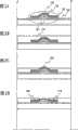
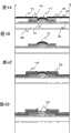
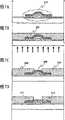
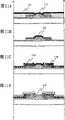
图1A-1D是解释根据本发明制造薄膜晶体管的步骤的剖面图;1A-1D are cross-sectional views explaining the steps of manufacturing a thin film transistor according to the present invention;
图2A-2D是解释根据本发明制造薄膜晶体管的步骤的剖面图;2A-2D are cross-sectional views explaining the steps of manufacturing a thin film transistor according to the present invention;
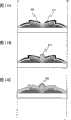
图3是根据本发明的薄膜晶体管的结构的顶视图;3 is a top view of the structure of a thin film transistor according to the present invention;
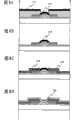
图4A-4D是解释根据本发明制造薄膜晶体管的步骤的剖面图;4A-4D are cross-sectional views explaining the steps of manufacturing a thin film transistor according to the present invention;
图5A-5D是解释根据本发明制造薄膜晶体管的步骤的剖面图;5A-5D are cross-sectional views explaining the steps of manufacturing a thin film transistor according to the present invention;
图6A-6D是解释根据本发明制造薄膜晶体管的步骤的剖面图;6A-6D are cross-sectional views explaining the steps of manufacturing a thin film transistor according to the present invention;
图7A-7D是解释根据本发明制造薄膜晶体管的步骤的剖面图;7A-7D are cross-sectional views explaining the steps of manufacturing a thin film transistor according to the present invention;
图8A-8D是解释根据本发明制造薄膜晶体管的步骤的剖面图;8A-8D are cross-sectional views explaining the steps of manufacturing a thin film transistor according to the present invention;
图9A-9D是解释根据本发明制造薄膜晶体管的步骤的剖面图;9A-9D are cross-sectional views explaining the steps of manufacturing a thin film transistor according to the present invention;
图10A-10D是解释根据本发明制造薄膜晶体管的步骤的剖面图;10A-10D are cross-sectional views explaining the steps of manufacturing a thin film transistor according to the present invention;
图11A-11D是解释根据本发明制造薄膜晶体管的步骤的剖面图;11A-11D are cross-sectional views explaining the steps of manufacturing a thin film transistor according to the present invention;
图12A-12D是解释根据本发明制造薄膜晶体管的步骤的剖面图;12A-12D are cross-sectional views explaining the steps of manufacturing a thin film transistor according to the present invention;
图13A-13D是解释根据本发明制造薄膜晶体管的步骤的剖面图;13A-13D are sectional views explaining the steps of manufacturing a thin film transistor according to the present invention;
图14A-14C是解释根据本发明制造薄膜晶体管的步骤的剖面图;14A-14C are sectional views explaining the steps of manufacturing a thin film transistor according to the present invention;
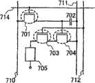
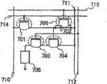
图15是可用于本发明的微滴排放设备结构的简图;Fig. 15 is a schematic diagram of the structure of a droplet discharge device usable in the present invention;
图16A-16D是显示可用于本发明的发光元件模型的简图;16A-16D are diagrams showing models of light-emitting elements that can be used in the present invention;
图17A-17F是显示可用于本发明的象素配置的等效电路图;17A-17F are equivalent circuit diagrams showing pixel configurations usable in the present invention;
图18A-18C是显示根据本发明安装显示设备驱动电路的方法的顶视图;18A-18C are top views showing a method of mounting a display device driving circuit according to the present invention;
图19A-19D是显示根据本发明安装显示设备驱动电路的方法的剖面图;19A-19D are cross-sectional views showing a method of mounting a display device driving circuit according to the present invention;
图20是显示在利用TFT形成根据本发明的显示面板扫描线驱动电路的实例中电路结构的简图;20 is a schematic diagram showing a circuit structure in an example in which a TFT is used to form a display panel scanning line driving circuit according to the present invention;
图21是显示在利用TFT形成根据本发明的显示面板扫描线驱动电路的实例中电路结构的简图(位移登记电路);21 is a diagram showing a circuit structure in an example of forming a scanning line driving circuit for a display panel according to the present invention using TFTs (displacement registration circuit);
图22是显示在利用TFT形成根据本发明的显示面板扫描线驱动电路的实例中电路结构的简图(缓冲电路);22 is a schematic diagram (buffer circuit) showing a circuit structure in an example of forming a display panel scanning line driving circuit according to the present invention using TFTs;
图23A-23C是显示根据本发明的发光显示模块结构的简图;23A-23C are diagrams showing the structure of a light-emitting display module according to the present invention;
图24是显示根据本发明的液晶显示模块的简图;24 is a schematic diagram showing a liquid crystal display module according to the present invention;
图25是解释电子装置结构的框图;25 is a block diagram explaining the structure of an electronic device;
图26是显示电子装置实例的简图;26 is a diagram showing an example of an electronic device;
图27A和27B是显示电子装置实例的简图。27A and 27B are diagrams showing examples of electronic devices.
具体实施方式Detailed ways
下文参考附图对本发明的实施模式进行说明。本发明能够以多种模式加以执行,本领域技术人员容易理解,在不背离本发明目的和范围的前提下能够对本文公开的实施模式和细节进行各种修改。本发明不应当认为限制于下文给出的实施例说明。而且,在所有附图中,相同的附图标记表示相同的部分,并不再进行进一步的解释。Embodiment modes of the present invention are described below with reference to the drawings. The present invention can be implemented in various modes, and it is easily understood by those skilled in the art that various modifications can be made to the implementation modes and details disclosed herein without departing from the purpose and scope of the present invention. The invention should not be considered limited to the examples given below. Also, the same reference numerals denote the same parts throughout the drawings, and no further explanation will be given.
根据本发明制造TFT的步骤说明如下。The steps of manufacturing a TFT according to the present invention are explained below.
[实施模式1][Implementation Mode 1]
在实施模式1中将说明使用内腐蚀制造沟道刻蚀TFT的方法。In Embodiment Mode 1, a method of manufacturing a channel-etched TFT using etch-back will be described.
图1A显示了用于在基片100上形成栅电极层的步骤。图1A示意地显示了纵向剖面图,而图3显示了相应于图1中线A-B的平面结构。FIG. 1A shows steps for forming a gate electrode layer on a
基片100可以是通过熔融法或漂浮法制造的无碱金属玻璃基片,例如硼硅酸钡玻璃、硼硅酸铝玻璃和硅酸铝玻璃、陶瓷基片、和能够耐受本制造工艺的处理温度的耐热塑料基片等。另外,可以采用半导体基片如单晶硅,如在表面上具有绝缘层的不锈金属的金属基片。作为基片100,可以使用面积为例如320mmx400mm,370mmx470mm,550mmx650mm,600mmx720mm,680mmx880mm,1000mmx1200mm,1100mmx1250mm或1150mmx1300mm的大尺寸基片。The
通过微滴排放方法排放一种含有导电材料的成分,在基片100上形成栅电极层101。作为用于形成该层的导电材料,可以使用金属,例如Ag,Au,Cu,Ni,Pt,Pd,Ir,Rh,W,Al,Ta,Mo,Cd,Zn,Fe,Ti,Si,Ge,Zr和Ba,卤化银细颗粒或分散剂纳米尺寸颗粒。此外,能够采用ITO(铟锡氧化物),含有硅氧化物作为一种成为的ITO,有机锡,氧化锌(ZnO),氮化钛(TiN)等,它们是通常用作透明导电层。为了降低电阻,根据比电阻值,优选地使用一种溶解有金、银和铜其中一种的溶剂。更优选地,使用低电阻的银或铜。此外,阻挡膜(barrier film)优选地与银或金联用,以防止污染。当使用铜作为布线时,阻挡膜可以用含氮的绝缘或导电物质形成,例如氮化硅、氧氮化硅、氮化铝、氮化钛和氮化钽(TaN)。阻挡层可以通过微滴排放方法形成。溶剂是有机溶剂或类似物。作为有机溶剂,有酯如丁基乙酸酯,醇如异丙醇,和酮如丙酮。通过控制溶剂的浓度或者通过添加表面活性剂等可以任意地调节表面张力和粘度。通过三维地并且无规则地堆积导电细颗粒形成导电层。也就是说,导电层包括三维聚集颗粒。因此,其表面略微不平坦。另外,通过对颗粒进行烘焙,细颗粒的直径会增加,因此导电层具有粗糙的表面。进一步,由有机物质形成的粘合剂保留在导电层内,这取决于加热温度、气氛和时间。A composition containing a conductive material is discharged to form a
可以在基片100上形成基膜,从而将栅电极层良好地粘着在基片上。基层可以通过溅射、汽相沉积等用金属材料,例如Ti(钛)、W(钨)、Cr(铬)、Ta(钽)、Ni(镍)和Mo(钼),或其氧化物形成。基层厚度可以为100nm或者更小。因为基层优选地尽可能地薄,所以基层不必具有层结构。如果栅电极层能够良好地粘着在基片上则可以消除基层。此外,可以执行大气压等离子体处理。除了这个步骤之外,当通过微滴排放方法在有机层、无机层、金属层等上形成导电层或者当通过微滴排放方法在导电层上形成有机层、无机层、金属层等时,可以提供基层,以便使每个导电层与其良好粘着。A base film can be formed on the
用于微滴排放方法的成分的粘度优选地设定为5-20mPa·s或者更小。这可以防止成分干燥,从而能够通过排放口平滑地排放成分。表面张力优选地设定为20-50mN/m。优选地根据所用溶剂和预期目的对成分的粘度等进行调节。例如,其中ITO或含有氧化硅、有机铟或有机锡的ITO溶解或分散在溶剂内的成分的粘度被设定为5-20mPa·s;其中银溶解或分散在溶剂中的成分的粘度被设定为5-20mPa·s;并且其中金分散在溶剂中的成分的粘度被设定为10-20mPa·s。The viscosity of the ingredients used in the droplet discharge method is preferably set at 5 to 20 mPa·s or less. This prevents ingredients from drying out, enabling smooth discharge of ingredients through the discharge port. The surface tension is preferably set at 20-50 mN/m. The viscosity and the like of the ingredients are preferably adjusted according to the solvent used and the intended purpose. For example, the viscosity of a composition in which ITO or ITO containing silicon oxide, organoindium, or organotin is dissolved or dispersed in a solvent is set to 5-20 mPa·s; the viscosity of a composition in which silver is dissolved or dispersed in a solvent is set to is set at 5-20 mPa·s; and the viscosity of the composition in which gold is dispersed in the solvent is set at 10-20 mPa·s.
导电粒子的直径优选地尽可能小,以防止阻塞喷嘴或用于制造微小图形,当然这取决于每个喷嘴的直径或图形形状。优选地,导电粒子的直径为0.1μm或者更小。成分用一种已知方法形成,例如电解、雾化和湿法还原(wet reducing)。粒子尺寸典型地为大约0.5-1.0μm。在使用气体蒸发方法的实例中,用分散剂保护的每个纳米尺寸分子极其细小,大小大约为7nm。进一步,当纳米尺寸粒子的每个表面覆盖有涂层剂时,室温下,纳米尺寸粒子在溶液中不会聚集,而是均匀地分散在溶剂中,显示与液体相似的性质。因此,优选地使用涂层剂。The diameter of the conductive particles is preferably as small as possible to prevent clogging of the nozzles or for making minute patterns, depending of course on the diameter or pattern shape of each nozzle. Preferably, the conductive particles have a diameter of 0.1 μm or less. The composition is formed using a known method such as electrolysis, atomization and wet reducing. The particle size is typically about 0.5-1.0 μm. In the example using the gas evaporation method, each nano-sized molecule protected with the dispersant is extremely fine, about 7 nm in size. Further, when each surface of the nanosized particles is covered with a coating agent, the nanosized particles do not aggregate in a solution at room temperature, but are uniformly dispersed in a solvent, showing properties similar to liquids. Therefore, a coating agent is preferably used.
成分排放步骤可以在减压下执行。当成分排放步骤在减压下执行时,在从排放该成分开始到它附着在被处理物体上为止的时间内,成分中的溶剂蒸发。因此,能够消除或缩短将在后面执行的用于干燥和烘焙步骤。在排放溶液之后,使用激光辐射、快速热退火、加热炉或类似物(这取决于溶液的种类)在常压或减压下执行干燥步骤和烘焙步骤其中之一或者两者。用于干燥和烘焙的步骤都是热处理步骤。例如,在100℃下干燥3分钟,而在200-350℃下烘焙15-120分钟;因此,其目的、温度和时间可以改变。可以预先对基片加热,从而顺利地执行用于干燥和烘焙的步骤。此时,尽管加热温度取决于基片材料等,但是一般设定为100-800℃(优选地为200-350℃)。在该步骤中,溶液中的溶剂被蒸发或者分散剂被化学除去,并且周围的树脂被固化和收缩,从而加速熔合和焊接。该步骤在氧气氛、氮气氛或空气下执行。优选地,该步骤在氧气氛下执行,从而容易除去其中的溶剂或分散有金属元素的溶剂。The component discharging step can be performed under reduced pressure. When the component discharge step is performed under reduced pressure, the solvent in the component evaporates during the time from when the component is discharged to when it adheres to the object to be processed. Therefore, steps for drying and baking to be performed later can be eliminated or shortened. After the solution is discharged, one or both of the drying step and the baking step are performed under normal pressure or reduced pressure using laser radiation, rapid thermal annealing, heating furnace or the like depending on the kind of the solution. The steps for drying and baking are all heat treatment steps. For example, drying is performed at 100°C for 3 minutes, while baking is performed at 200-350°C for 15-120 minutes; therefore, its purpose, temperature and time can be changed. The substrate can be heated in advance, so that the steps for drying and baking can be performed smoothly. At this time, although the heating temperature depends on the substrate material and the like, it is generally set at 100-800°C (preferably 200-350°C). In this step, the solvent in the solution is evaporated or the dispersant is chemically removed, and the surrounding resin is cured and shrunk, thereby accelerating fusion and welding. This step is performed under an oxygen atmosphere, nitrogen atmosphere or air. Preferably, this step is performed under an oxygen atmosphere so that the solvent or the solvent in which the metal element is dispersed is easily removed.
图15显示了用于形成图形的微滴排放设备的模型。微滴排放设备603的各个压头605和612与控制装置607相连。通过用计算机610控制各个压头,能够预先写入在计算机中编程的预定图形。例如,布线图形的位置可以参考在基片600上提供的标记611加以确定。选择地,基片600的边缘可以确定作为参考点。通过成像装置604,例如利用电荷耦合器件(CCD)或互补金属氧化物半导体(CMOS)的图像传感器,检测有关标记611的信息,并通过图像处理装置609将其转变成数字信号。当通过计算机610识别数字信号时,产生控制信号并发送给控制装置607。当然,将在基片600上形成的图形信息存储在记录介质608上。根据有关图形的信息将控制信号发送给控制装置607,从而微滴排放装置603的压头605和612能够单独加以控制。排放材料从材料供应源613和614通过管道提供给压头605和612。可以使用能够通过压头单独地排放金属材料、有机材料和无机材料的设备,从而能够通过喷墨压头排放R、G和B各个颜色,类似场致发光(EL)。因此,当通过微滴排放装置形成层间绝缘层时,可以通过相同的材料多层布置(multiply-layered)薄内衬(thin line),以提高吞吐量。尽管微滴排放装置603中平行布置的压头605和612的纵向相应于图15中基片的宽度,但是该微滴排放装置能够通过分别扫描压头,在宽度大于压头605和612纵向长度的大尺寸基片上形成图形。在这种实例中,压头605和612能够沿着图15箭头所示方向自由地加以扫描,从而能够自由设定被写入区域。因此,能够在基片上写入多个相同的图形。Fig. 15 shows a model of a droplet discharge device for forming patterns. The
在本实施模型中,栅电极层是通过微滴排放装置形成的,然而它也可以通过CVD或溅射形成。In this embodiment model, the gate electrode layer is formed by a droplet discharge device, however it may also be formed by CVD or sputtering.
在形成导电基层时,优选地执行如下两个步骤中的任何一个用于处理暴露的基层。In forming the conductive base layer, it is preferable to perform any one of the following two steps for treating the exposed base layer.
第一个方法是用于绝缘没有被栅电极层重叠的基层的步骤。具体地讲,氧化没有被栅电极层重叠的基层以便被绝缘。当基层被氧化而被绝缘时,基层优选的厚度为10nm或更小。这能够容易地氧化基层。关于氧化基层的方法,能够采样将其暴露在氧气气氛下的方法或者执行热处理的方法。The first method is a step for insulating the base layer which is not overlapped by the gate electrode layer. Specifically, the base layer not overlapped by the gate electrode layer is oxidized so as to be insulated. When the base layer is oxidized to be insulated, the base layer preferably has a thickness of 10 nm or less. This can easily oxidize the base layer. Regarding the method of oxidizing the base layer, a method of exposing it to an oxygen atmosphere or a method of performing heat treatment can be sampled.
第二个方法是利用栅电极层作为掩模,通过刻蚀除去基层的步骤。在采用该步骤时,基层的厚度不受限制。The second method is a step of removing the base layer by etching using the gate electrode layer as a mask. The thickness of the base layer is not limited when this step is employed.
接着,通过等离子体CVD或溅射形成栅绝缘层102,其具有单层或叠层结构(见图1B)。作为一个优选模式,栅绝缘层的形成是通过层压一个由氮化硅形成的绝缘层,一个由氧化硅形成的绝缘层和另一个由氮化硅形成的绝缘层。为了在低温下形成具有低栅极泄漏电流的致密绝缘层,可以在待形成的绝缘层中混合添加有稀有气体元素,例如氩的反应气体。通过用氮化硅或氧氮化硅形成与栅电极层101接触的第一层,可以防止由于氧化造成的退化。而且,通过使用NiB(硼化镍)作为与栅电极层101接触的第一层,可以使其表面变得光滑。Next, a
随后,形成半导体层103。关于用于形成半导体层103的材料,可以采用通过气相生长方法或溅射用半导体材料气体(典型的是硅烷或锗烷)制造的非晶半导体(下文称作AS);通过利用光能或热能对非晶半导体进行结晶形成的多晶半导体;半非晶(也称作微晶)半导体(下文称作SAS)或类似物。此外,能够使用有机半导体。Subsequently, the
SAS在非晶结构和晶体结构(包括单晶结构和多晶结构)之间具有中间结构,并具有就自由能来说稳定的第三条件。SAS进一步包括具有短程有序的晶体区,同时具有点阵畸变。至少在半非晶半导体膜的一部分内能够观察到大小为0.5-20nm的晶体区。在以硅作为主要组分的实例中,拉曼光谱向小于520cm-1的低波数迁移。通过X-射线衍射,在SAS中可以观察到被认为得自于硅晶体点阵的(111)和(220)的衍射峰。SAS中含有原子百分数至少为1%或者更多的氢或卤素,以终止悬挂键。SAS是通过硅化物气体的辉光放电分解(等离子体CVD)形成的。关于硅化物气体,可以使用SiH4,Si2H6,SiH2Cl2,SiHCl3,SiCl4,SiF4或类似物。硅化物气体可以和GeF4混合。硅化物气体还可以用H2或H2与He,Ar,Kr和Ne中的一种或多种稀有气体的混合物加以稀释。此外,硅化物气体可以和GeF4混合。硅化物气体还可以用F2或F2与He,Ar,Kr和Ne中的一种或多种稀有气体元素的混合物加以稀释。稀释比例的范围设定为1∶2-1∶1000。压力范围设定为大约0.1-133Pa。功率频率设定为1-120MHz,优选地为13-60MHz。基片加热温度可以设定为300℃或者更低。关于膜中含有的杂质元素,对于大气成分如氧、氮和碳,每种杂质的浓度优选地设定为1x1020/cm3或者更低。特别地,氧浓度设定为5x1019/cm3或者更低,优选地1x1019/cm3或者更低。SAS has an intermediate structure between an amorphous structure and a crystalline structure (including a single crystal structure and a polycrystalline structure), and has a third condition of being stable in terms of free energy. The SAS further includes crystalline regions with short-range order, while having lattice distortions. A crystalline region having a size of 0.5 to 20 nm can be observed in at least a part of the semi-amorphous semiconductor film. In the case of silicon as the main component, the Raman spectrum shifts to low wavenumbers less than 520 cm−1 . By X-ray diffraction, diffraction peaks of (111) and (220) believed to be derived from silicon crystal lattices can be observed in SAS. The SAS contains at least 1 atomic percent or more of hydrogen or halogen to terminate dangling bonds. SAS is formed by glow discharge decomposition (plasma CVD) of silicide gas. As for the silicide gas, SiH4 , Si2 H6 , SiH2 Cl2 , SiHCl3 , SiCl4 , SiF4 or the like can be used. Silicide gas can be mixed with GeF4 . The silicide gas can also be diluted withH2 or a mixture ofH2 and one or more noble gases among He, Ar, Kr and Ne. In addition, silicide gas can be mixed with GeF4 . The silicide gas can also be diluted withF2 or a mixture ofF2 and one or more rare gas elements in He, Ar, Kr and Ne. The range of the dilution ratio is set at 1:2-1:1000. The pressure range is set at about 0.1-133Pa. The power frequency is set to 1-120MHz, preferably 13-60MHz. The substrate heating temperature can be set to 300°C or lower. Regarding impurity elements contained in the film, the concentration of each impurity is preferably set to 1×10²⁰ /cm3 or lower for atmospheric components such as oxygen, nitrogen, and carbon. In particular, the oxygen concentration is set to 5×10¹⁹ /cm3 or lower, preferably 1×10¹⁹ /cm3 or lower.
通过加热或激光辐射使非晶半导体层或SAS结晶,能够形成晶体半导体层。选择地,可以直接形成晶体半导体层。在这种情况下,晶体半导体层是通过使用含氟气体,例如GeF4和F2,和硅烷气体,例如SiH4和Si2H6,并通过加热或等离子体直接形成的。A crystalline semiconductor layer can be formed by crystallizing an amorphous semiconductor layer or SAS by heating or laser irradiation. Alternatively, a crystalline semiconductor layer may be directly formed. In this case, the crystalline semiconductor layer is directly formed by heating or plasma by using fluorine-containing gas, such as GeF4 and F2 , and silane gas, such as SiH4 and Si2 H6 .
当采用等离子体CVD时,利用一种半导体材料气体,例如SiH4和SiH4与H2的混合物形成AS。在使用其中SiH4用H2稀释3-1000倍的混合气体时或者在使用其中Si2H6和GeF4的稀释比例为20-40∶0.9的混合气体时,能够获得Si成分比例为80%或者更高的SAS。特别地,后一情况是优选的,因为可以从基膜的界面向半导体层103进行结晶。选择地,可以采用SiH4和F2混合气体。When plasma CVD is employed, AS is formed using a semiconductor material gas such as SiH4 and a mixture of SiH4 and H2 . When using a mixed gas in which SiH4 is diluted 3-1000 times with H2 or when using a mixed gas in which the dilution ratio of Si2 H6 and GeF4 is 20-40:0.9, a Si composition ratio of 80% can be obtained Or higher SAS. In particular, the latter case is preferable because crystallization can proceed from the interface of the base film toward the
接着,在半导体层103上形成含有一种导电类型杂质的半导体层104。含有一种导电类型杂质的半导体层104可以用硅烷气体和磷化氢气体形成,并由AS或SAS形成。Next, a
接着通过微滴排放方法在含有一种导电类型杂质的半导体层104上形成掩模105。利用掩模105,对含有一种导电类型杂质的半导体层104和半导体层103进行刻蚀(见图1C和1D)。Next, a
使用树脂材料作为掩模,例如环氧树脂、丙烯树脂、苯树脂、酚醛树脂、三聚氰胺树脂和聚氨酯树脂。选择地,掩模可以用如下的材料制造:有机材料,例如具有高光透射性质的苯环丁烯、聚对二甲苯、法兰绒(flare)和聚酰亚胺;包括通过聚合作用形成的化合物的材料,例如硅氧烷聚合物;含有可溶于水的均匀聚合物和可溶于水的共聚合物的材料;和类似物。此外,也可以使用商业上可以获得的含有光敏剂的抗蚀剂材料。例如,可以使用典型的正抗蚀剂,包括酚醛树脂和光敏剂吩嗪化合物;负抗蚀剂包括,包括碱树脂(base resin)、二苯基硅烷二醇(diphenylsilanediol)和产酸材料等。通过控制溶剂浓度或者通过添加表面活性剂可以适当地调节任何材料的表面张力和粘度。Use resin materials such as epoxy, acrylic, benzene, phenolic, melamine, and polyurethane resins as masks. Alternatively, the mask can be fabricated from organic materials such as benzenecyclobutene, parylene, flare, and polyimide with high light transmission properties; including compounds formed by polymerization materials such as silicone polymers; materials comprising water-soluble homogeneous polymers and water-soluble copolymers; and the like. In addition, commercially available resist materials containing photosensitizers can also be used. For example, typical positive resists including phenolic resins and photosensitizer phenazine compounds; negative resists including base resins, diphenylsilanediol, and acid-generating materials can be used. The surface tension and viscosity of any material can be properly adjusted by controlling the solvent concentration or by adding surfactants.
随后,除去掩模105,用于形成半导体区106(见图2A)。Subsequently, the
接着,施加平面化(planarizing)膜107(见图2B)。作为平面化膜107的材料,可以引用如下的材料:树脂材料,例如环氧树脂、丙烯酸树脂、苯酚树脂、酚醛树脂、三聚氰胺树脂和聚氨脂树脂;有机材料,例如具有高光透射性质的苯环丁烯、聚对二甲苯、法兰绒和聚酰亚胺;包括通过聚合作用形成的化合物的材料,例如硅氧烷聚合物;含有可溶于水的均匀聚合物和可溶于水的共聚合物的材料;和类似物。此外,也可以使用商业上可以获得的含有光敏剂的抗蚀剂材料。例如,可以使用典型的正抗蚀剂,包括酚醛树脂和光敏剂吩嗪化合物;负抗蚀剂包括,包括碱树脂(base resin)、二苯基硅烷二醇(diphenylsilanediol)和产酸材料等。通过控制溶剂浓度或者通过添加表面活性剂可以适当地调节任何材料的表面张力和粘度。Next, a
对平面化膜107进行内腐蚀。因为在基片上形成了栅电极层101,所以位于栅电极层101上面的平面化膜厚度变薄(见图2B)。因此,位于沟道部分108上面的平面化膜只能通过内腐蚀加以选择性除去(见图2C)。The
利用剩余的平面化膜作为掩模,对含有一种导电类型杂质的半导体层104进行刻蚀,从而形成含有一种导电类型杂质的半导体层109和110(见图2D)。因此,以自对准的方式形成和使用用于刻蚀含有一种导电类型杂质的半导体层的掩模。Using the remaining planarization film as a mask, the
在用SAS形成半导体层时,可以采用其中栅电极被源极区和漏极区覆盖的能够以高速驱动TFT的结构;其中源极区和漏极区的边缘相应于栅电极的边缘的所谓自对准结构;或者其中源极区和漏极区以某种特定间隔独立地形成,而不覆盖栅电极的具有降低截止电流(off-current)效果的结构。In forming the semiconductor layer with SAS, a structure capable of driving a TFT at high speed in which the gate electrode is covered with a source region and a drain region can be employed; a so-called free-standing structure in which the edges of the source region and the drain region correspond to the edges of the gate electrode. an alignment structure; or a structure having an off-current reducing effect in which a source region and a drain region are independently formed at a certain interval without covering a gate electrode.
接着,形成具有不同润湿性的区域。润湿性差异指示了目标区和非目标区之间的相对关系。两个区域的润湿性以及在目标区内形成的材料均可以不同。不同润湿性的区域是指其中与待形成材料的接触角彼此不同的区域。与该材料之间具有较大接触角的区域是低润湿性的区域(下文称作具有低润湿性的区域),而该材料之间具有较小接触角的区域是高润湿性的区域(下文称作具有高润湿性的区域)。当区域具有大接触角时,具有流动性的液体成分不会在该区域的表面上扩散;因此,其表面不被润湿。选择地,当区域具有小接触角时,具有流动性的液体成分将在该区域的表面上扩散,从而其表面被润湿。在本发明中,不同润湿性区域之间接触角的差为30℃或者更大,优选地为40℃或者更大。Next, regions with different wettability are formed. Differences in wettability indicate the relative relationship between target and non-target areas. The wettability of the two regions as well as the material formed in the target region can be different. The regions of different wettability refer to regions in which the contact angles with the material to be formed are different from each other. A region with a larger contact angle with the material is a region of low wettability (hereinafter referred to as a region with low wettability), while a region with a smaller contact angle with the material is a region with high wettability region (hereinafter referred to as the region with high wettability). When a region has a large contact angle, a fluid liquid component does not spread on the surface of the region; therefore, its surface is not wetted. Alternatively, when a region has a small contact angle, the fluid component will spread over the surface of the region, thereby wetting the surface. In the present invention, the difference in contact angle between regions of different wettability is 30°C or more, preferably 40°C or more.
首先,排放或施加用于形成低润湿性区域的溶液(见图4A)。作为用于形成低润湿性区域的溶液成分的实例,使用一种硅烷耦合剂,用化学式Rn-Si-X(4-n)(n=1,2,3)表示。在该化学式中,R表示含有相对不活跃基团,例如烃基的物质。进一步,X表示能够通过浓缩水解并与存在于基片表面上的羟基或吸附水结合的物质,例如卤基、甲氧基、乙氧基和乙酸基。First, the solution for forming the low-wettability region is drained or applied (see FIG. 4A ). As an example of a solution component for forming the low-wettability region, a silane coupling agent represented by the chemical formulaRn -Si-X(4-n) (n=1, 2, 3) is used. In this formula, R represents a substance containing a relatively inactive group, such as a hydrocarbon group. Further, X represents a substance capable of being hydrolyzed by concentration and bonded to a hydroxyl group or adsorbed water present on the surface of the substrate, such as a halogen group, a methoxy group, an ethoxy group and an acetate group.
作为硅烷耦合剂的代表性实例,在使用以氟烷基为R的氟硅烷耦合剂(例如氟烷基硅烷(FAS))的实例中,润湿性能够被进一步降低。FAS中的R具有如下表示的结构(CF3)(CF2)x(CH2)y(x是0-10的整数,y是0-4的整数)。当多个R或X与Si结合时,R或X可以相互相同或不同。典型地,能够使用的氟烷基硅烷(下文称作FAS)例如:氟十七烷四氢乙酸基三乙氧基硅烷(heptadecafluoro tetrahydrodecyltriethoxysilane);氟十七烷四氢乙酸基三氯硅烷(heptadecafluorotetrahydrodecyl trichlorosiane);氟十三烷四氢辛烷基三氯硅烷(tridecafluoro tetrahydrooctyl trichlorosiane);和三氟丙基三甲氧基硅烷(trifluoropropyl trimethoxysilane)。As a representative example of the silane coupling agent, in the case of using a fluorosilane coupling agent having a fluoroalkyl group as R (such as fluoroalkylsilane (FAS)), wettability can be further reduced. R in FAS has a structure represented as follows (CF3 )(CF2 )x (CH2 )y (x is an integer of 0-10, and y is an integer of 0-4). When a plurality of R or X is combined with Si, R or X may be the same as or different from each other. Typically, the fluoroalkylsilane (hereinafter referred to as FAS) that can be used is for example: fluoroheptadecafluoro tetrahydrodecyltriethoxysilane (heptadecafluoro tetrahydrodecyltriethoxysilane); ); tridecafluoro tetrahydrooctyl trichlorosilane; and trifluoropropyl trimethoxysilane.
作为用于形成低润湿性区域的溶液的溶剂,能够使用碳氢化合物溶剂,例如n戊烷、n己烷、n庚烷、n辛烷、n癸烷、二环戊烷、苯、甲苯、二甲苯、四甲基苯、茚、四氢萘、十氢萘和异三十烷、四氢弗兰或类似物。As a solvent for the solution forming the low wettability region, hydrocarbon solvents such as n-pentane, n-hexane, n-heptane, n-octane, n-decane, dicyclopentane, benzene, toluene can be used , xylene, tetramethylbenzene, indene, tetrahydronaphthalene, decahydronaphthalene and isotriaconane, tetrahydrofuran or similar.
作为用于形成低润湿性区域的溶液的成分实例,可以使用一种具有碳氟链的材料(例如碳氟树脂)。关于碳氟树脂,可以使用如下物质:聚四氟乙烯(PTFE);全氟烷氧烷(PFA);全氟(乙烯丙稀)共聚物(PFEP);乙烯-四氟乙烯共聚物(ETFE);聚(亚乙烯基氟化物)(PVDF);聚氯三氟乙烯(PCTFE);乙烯-氯三氟乙烯共聚物(ECTFE);聚四氟乙烯-全氟间二氧环杂戊烯(perfluorodioxole)共聚物(TFE/PDD);聚(氟乙烯)(PVF)等。As an example of the composition of the solution for forming the low-wettability region, a material having a fluorocarbon chain (such as a fluorocarbon resin) can be used. As for fluorocarbon resins, the following can be used: Polytetrafluoroethylene (PTFE); Perfluoroalkane (PFA); Perfluoro(ethylene propylene) copolymer (PFEP); Ethylene-tetrafluoroethylene copolymer (ETFE) ; poly(vinylidene fluoride) (PVDF); polychlorotrifluoroethylene (PCTFE); ethylene-chlorotrifluoroethylene copolymer (ECTFE); polytetrafluoroethylene-perfluorodioxole (perfluorodioxole ) copolymer (TFE/PDD); poly(vinyl fluoride) (PVF), etc.
接着,冲洗该附着有溶液的用于形成低润湿性区域的表面,从而形成极薄的具有低润湿性的表面111。Next, the surface for forming the low-wettability region to which the solution is attached is rinsed, thereby forming an extremely
具有低润湿性的表面111还可以使用不同的方法加以形成,例如汽相沉积,而不是排放或施加用于形成低润湿性区域的溶液。The
接着,通过湿法刻蚀等除去剩余的平面化膜。此时,平面化膜上具有低润湿性的区域也通过剥离(lift off)加以除去,从而具有低润湿性的区域仅存在于沟道部分112上(见图4B)。Next, the remaining planarizing film is removed by wet etching or the like. At this time, the region with low wettability on the planarizing film is also removed by lift off, so that the region with low wettability exists only on the channel portion 112 (see FIG. 4B ).
随后,通过微滴排放方法选择性排放含有导电材料的成分用于形成源极和漏极布线113和114(见图4C)。此时,当排放成分使之包夹沟道部分112时,排放在低润湿性区域内的液滴不稳定,并从低润湿性区域和高润湿性区域之间的边界向高润湿性区域移动。因此,在高润湿性区域内能够选择性形成图形,从而能够以自对准的方法确定源极和漏极布线的位置。另外,能够使用一种主要含有金属颗粒,例如Ag(银)、Au(金)、Cu(铜)、W(钨)和Al(铝)的成分作为导电材料,用于形成这些布线。此外,可以组合使用光透射铟锡氧化物(ITO),包括铟锡氧化物和氧化硅的ITSO,有机铟,有机锡,氧化锌,氮化钛等。Subsequently, a composition containing a conductive material is selectively discharged by a droplet discharge method for forming source and drain
接着通过刻蚀等除去用于形成具有低润湿性区域112的极薄膜。Next, the extremely thin film for forming the
优选地在源极和漏极布线113和114上形成钝化层115。钝化层可以通过用于形成薄膜的方法,例如等离子体CVD和溅射加以形成,并使用氮化硅、氧化硅、氮氧化硅、氧氮化硅、氧氮化铝、氧化铝、金刚石如碳(DLC)、氮化碳(CN)、其它绝缘材料等。A
根据上述的步骤,能够制造一种沟道刻蚀TFT(见图4D)。According to the above steps, a channel-etched TFT can be manufactured (see FIG. 4D).
[实施模式2][Implementation Mode 2]
在实施模式2中将说明使用内腐蚀制造沟道停止TFT的方法。In
通过微滴排放方法在基片100上排放一种含有导电材料的成分,从而形成栅电极层201(见图5A)。通过等离子体CVD或溅射形成包括单层或叠层结构的栅绝缘层202。作为一个具体的优选模型,通过层压三个层形成栅绝缘层,即一个用氮化硅制成的绝缘层,一个用氧化硅制成的绝缘层,和另一个用氮化硅制成的绝缘层。接着形成半导体层203。上述的步骤与实施模式1相同。A composition containing a conductive material is discharged on the
通过等离子体CVD或溅射在半导体层203上形成绝缘层204。如在随后的步骤中显示的,绝缘层204保留在与栅电极层相关的半导体层203上,从而用作沟道保护层。沟道保护层具有保护含有一种导电类型杂质的半导体层免受损伤并保持界面清洁的有利效果,从而防止半导体层203被杂质污染,例如有机材料、金属和水蒸气。因此,绝缘层204优选地用致密膜形成。氮化硅膜是优选的,其是通过辉光放电分解使用用稀有气体元素例如氩稀释100倍-500倍的硅化物气体制成的,因为它在100℃或更低的温度下将成为致密膜。如果需要,可以用层压结构形成绝缘层204。The insulating
在绝缘层204上选择性排放一种成分,从而在相应于栅电极层201的位置形成掩模205(见图5B)。使用树脂材料,例如环氧树脂、丙烯酸树脂、苯树脂、酚醛树脂、三聚氰胺树脂和聚氨酯树脂作为掩模205。选择地,可以使用微滴排放方法用有机材料制造掩模,例如具有光透射性质的苯环丁烯、聚对二甲苯、法兰绒和聚酰亚胺;包括通过聚合作用形成的化合物的材料,例如硅氧烷聚合物;含有可溶于水的均匀聚合物和可溶于水的共聚合物的材料;和类似物。此外,也可以使用商业上可以获得的含有光敏剂的抗蚀剂材料。例如,可以使用典型的正抗蚀剂,包括酚醛树脂和光敏剂吩嗪化合物;负抗蚀剂包括,包括碱树脂(base resin)、二苯基硅烷二醇(diphenylsilanediol)和产酸材料等。通过控制溶剂浓度或者通过添加表面活性剂等可以适当地调节任何材料的表面张力和粘度。A component is selectively discharged on the insulating
利用掩模205对绝缘层204进行刻蚀,从而形成绝缘层206,其起到沟道保护层的作用(见图5C)。除去掩模205。在半导体层203和绝缘层206上形成含有一种导电类型杂质的半导体层207。含有一种导电类型杂质的半导体层207可以用硅烷气体和磷化氢气体制成,并能够用AS或SAS形成。The insulating
随后的步骤与实施模式1的步骤相同。Subsequent steps are the same as those for implementing Mode 1.
根据上述步骤,能够制造一种沟道停止TFT。According to the above steps, a channel stop TFT can be manufactured.
[实施模式3][Implementation Mode 3]
在实施模式3中将说明使用后表面曝光步骤制造沟道刻蚀TFT的方法。In Embodiment Mode 3, a method of manufacturing a channel-etched TFT using a post-surface exposure step will be described.
图6A显示了在基片100上形成栅电极层的步骤。图6A图解了示意性纵剖面图,而图3图解了相应于线A-B的顶平面结构。FIG. 6A shows a step of forming a gate electrode layer on a
通过微滴排放方法在基片100上排放含有导电材料的成分从而形成栅电极层301。另外,可以通过溅射或汽相沉积在基片100上形成用金属材料,如Ti(钛)、W(钨)、Cr(铬)、Ta(钽)、Ni(镍)和Mo(钼)或其氧化物形成的基层,使得栅电极层与基片良好粘着。在形成导电基层时,需要对没有与栅电极层重叠的基层进行氧化绝缘,或通过刻蚀加以除去,同时利用栅电极层作为掩模。A composition containing a conductive material is discharged on the
接着通过等离子体CVD或溅射形成栅绝缘层302,使具有单层或叠层结构(见图6B)。特别地,栅绝缘层302优选地通过层压3个层加以形成:一个用氮化硅制成的绝缘层,一个用氧化硅制成的绝缘层,和另一个用氮化硅制成的绝缘层。Next, a
接着形成半导体层303。作为用于形成半导体层303的材料,可以采用通过气相生长方法或溅射用半导体材料气体(典型的是硅烷或锗烷)制造的非晶半导体(下文称作AS);通过利用光能或热能对非晶半导体进行结晶形成的多晶半导体;半非晶(也称作微晶)半导体(下文称作SAS)或类似物。此外,能够使用有机半导体。Next, the
接着,在半导体层303上形成含有一种导电类型杂质的半导体层304。该含有一种导电类型杂质的半导体层304可以用硅烷气体和磷化氢气体形成,并能够由AS或SAS形成。Next, a
通过微滴排放方法在含有一种导电类型杂质的半导体层304上形成掩模305。利用掩模305,对含有一种导电类型杂质的半导体层304和半导体层303进行刻蚀(见图6C和6D)。A
随后,除去掩模305,从而形成半导体区306(见图7A)。Subsequently, the
接着,施加抗蚀剂307(见图7B)。关于用于抗蚀剂的材料,也可以采用含有光敏剂的商业上可获得的负抗蚀剂材料。例如,可以使用一种典型的负抗蚀剂,包括碱树脂、二苯基硅烷二醇(diphenylsilanediol)和产酸材料等。通过控制溶剂浓度或者通过添加表面活性剂可以适当地调节任何材料的表面张力和粘度。Next, a resist 307 is applied (see FIG. 7B). As for the material used for the resist, a commercially available negative resist material containing a photosensitizer can also be used. For example, a typical negative resist including alkali resin, diphenylsilanediol, acid generating material and the like can be used. The surface tension and viscosity of any material can be properly adjusted by controlling the solvent concentration or by adding surfactants.
然后,从基片的后表面对抗蚀剂307进行曝光(见图7B)。因为基片上面存在栅电极层301,所以栅电极层301上面的抗蚀剂不被曝光。因此,只能够通过显影选择地除去位于沟道部分308上面的抗蚀剂(见图7C)。Then, the resist 307 is exposed from the back surface of the substrate (see FIG. 7B). Since the
利用剩余的抗蚀剂309和310作为掩模,对含有一种导电类型杂质的半导体层304进行刻蚀,从而形成含有一种导电类型杂质的半导体层311和312(见图7D)。因此,以自对准的方式形成和使用用于刻蚀含有一种导电类型杂质的半导体层的掩模。Using the remaining resists 309 and 310 as masks, the
选择地,可以采用含有光敏剂的商业上可获得的负抗蚀剂材料作为掩模305。利用掩模305,刻蚀含有一种导电类型杂质的半导体层304和半导体层303。随后,从基片的后表面对掩模305进行曝光。因为基片上面存在栅电极层301,所以位于栅电极层301上面的含有光敏剂的抗蚀剂不被曝光。因此,只能够通过显影选择地除去位于沟道部分308上面的抗蚀剂(见图7C)。利用剩余的含有光敏剂的掩模,对含有一种导电类型杂质的半导体层304进行刻蚀,从而形成含有一种导电类型杂质的半导体层311和312。在这种情况下,可以省略形成抗蚀剂307的步骤。Alternatively, a commercially available negative resist material containing a photosensitizer can be used as the
随后的步骤与实施模式1中相同(见图8A,8B和8C)。Subsequent steps are the same as in Embodiment Mode 1 (see FIGS. 8A, 8B and 8C).
根据上述步骤,能够制造沟道刻蚀TFT(见图8D)。According to the above steps, a channel-etched TFT can be manufactured (see FIG. 8D ).
[实施模式4][Implementation Mode 4]
在实施模式4中将说明使用后表面曝光制造沟道停止TFT的方法。In
通过微滴排放方法在基片100上排放一种含有导电材料的成分,从而形成栅电极层201(见图5A)。接着,通过等离子体CVD或溅射形成栅绝缘层202,使其具有单层或叠层结构。优选地,通过层压三个层形成该栅绝缘层,即一个用氮化硅制成的绝缘层,一个用氧化硅制成的绝缘层,和另一个用氮化硅制成的绝缘层。然后形成半导体层203。上述的步骤与实施模式3相同。A composition containing a conductive material is discharged on the
通过等离子体CVD或溅射在半导体层203上形成绝缘层204。如在随后的步骤中显示的,绝缘层204保留在与栅电极层相关的半导体层上,从而用作沟道保护层。沟道保护层具有保护含有一种导电类型杂质的半导体层免受损伤并保持界面清洁的有利效果,从而防止半导体层203被杂质污染,例如有机材料、金属和水蒸气。因此,绝缘层204优选地用致密膜形成。氮化硅膜是优选的,其是通过辉光放电分解使用用稀有气体元素例如氩稀释100倍-500倍的硅化物气体制成的,因为它在100℃或更低的温度下将成为致密的膜。如果需要,可以用叠层结构形成绝缘层。The insulating
在绝缘层204与栅电极层201上选择性排放一种成分,从而在相应于栅电极层201的部分形成掩模205(见图5B)。使用树脂材料,例如环氧树脂、丙烯酸树脂、苯树脂、酚醛树脂、三聚氰胺树脂和聚氨酯树脂作为掩模205。选择地,可以使用微滴排放方法用有机材料制造掩模,例如具有光透射性质的苯环丁烯、聚对二甲苯、法兰绒和聚酰亚胺;包括通过聚合作用形成的化合物的材料,例如硅氧烷聚合物;含有可溶于水的均匀聚合物和可溶于水的共聚合物的材料;和类似物。此外,也可以使用商业上可以获得的含有光敏剂的抗蚀剂材料。例如,可以使用典型的正抗蚀剂,包括酚醛树脂和光敏剂吩嗪化合物;负抗蚀剂包括,包括碱树脂(base resin)、二苯基硅烷二醇(diphenylsilanediol)和产酸材料等。通过控制溶剂浓度或者通过添加表面活性剂等可以适当地调节任何材料的表面张力和粘度。A component is selectively discharged on the insulating
利用掩模205对绝缘层204进行刻蚀,从而形成绝缘层206,其起到沟道保护层的作用(见图5C)。除去掩模205。在半导体层203和绝缘层206上形成含有一种导电类型杂质的半导体层207。该含有一种导电类型杂质的半导体层207可以用硅烷气体和磷化氢气体制成,并能够用AS或SAS形成。The insulating
随后的步骤与实施模式3的步骤相同。具体地讲,施加抗蚀剂307(见图7B)。作为用于抗蚀剂的材料,可以采用商业上可获得的含光敏剂的负抗蚀剂材料。例如可以使用典型的负抗蚀剂,包括碱树脂、二苯基硅烷二醇(diphenylsilanediol)和产酸材料等。通过控制溶剂浓度或者通过添加表面活性剂可以适当地调节任何材料的表面张力和粘度。The subsequent steps are the same as those for implementing Mode 3. Specifically, resist 307 is applied (see FIG. 7B). As a material for the resist, a commercially available photosensitizer-containing negative resist material can be used. For example, typical negative resists including alkali resins, diphenylsilanediol, acid generating materials, and the like can be used. The surface tension and viscosity of any material can be properly adjusted by controlling the solvent concentration or by adding surfactants.
接着,从基片的后表面对抗蚀剂307进行曝光(见图7B)。因为基片上面存在栅电极层301,所以栅电极层301上面的抗蚀剂不被曝光。因此,只能够通过显影选择地除去位于沟道部分308上面的抗蚀剂(见图7C)。Next, the resist 307 is exposed to light from the back surface of the substrate (see FIG. 7B). Since the
利用剩余的抗蚀剂309和310作为掩模,对含有一种导电类型杂质的半导体层304进行刻蚀,从而形成含有一种导电类型杂质的半导体层311和312(见图7D)。因此,以自对准的方式形成和使用用于刻蚀含有一种导电类型杂质的半导体层的掩模。Using the remaining resists 309 and 310 as masks, the
选择地,可以采用商业上可获得的含有光敏剂的负抗蚀剂材料作为掩模305。利用掩模305,刻蚀含有一种导电类型杂质的半导体层304和半导体层303。随后,从基片的后表面对掩模305进行曝光。因为基片上面存在栅电极层301,所以位于栅电极层301上面的含有光敏剂的抗蚀剂不被曝光。因此,只能够通过显影选择地除去位于沟道部分308上面的抗蚀剂(见图7C)。利用剩余的含有光敏剂的掩模,对含有一种导电类型杂质的半导体层304进行刻蚀,从而形成含有一种导电类型杂质的半导体层311和312。在这种情况下,可以省略形成抗蚀剂307的步骤。Alternatively, a commercially available negative resist material containing a photosensitizer can be used as the
随后的步骤与实施模式1中相同。形成源极布线113和漏极布线114,并在源极和漏极布线上形成钝化层115。Subsequent steps are the same as in Embodiment Mode 1. A
根据上述步骤,能够制造沟道停止TFT(见图5D)。According to the above steps, a channel stop TFT can be manufactured (see FIG. 5D ).
[实施模式5][Implementation Mode 5]
在实施模式5中将说明使用顶表面曝光步骤制造沟道刻蚀TFT的方法。In Embodiment Mode 5, a method of manufacturing a channel-etched TFT using a top surface exposure step will be described.
图9A显示了在基片100上形成栅电极层的步骤。图9A图解了示意性纵剖面图,而图3图解了相应于线A-B的顶平面结构。FIG. 9A shows a step of forming a gate electrode layer on a
通过微滴排放方法在基片100上排放含有导电材料的成分从而形成栅电极层301。通过溅射或汽相沉积在基片100上形成用金属材料,如Ti(钛)、W(钨)、Cr(铬)、Ta(钽)、Ni(镍)和Mo(钼)或其氧化物形成的基层,使得栅电极层与基片良好粘着。在形成导电基层时,需要对没有与栅电极层重叠的基层进行氧化绝缘,或通过刻蚀加以除去,同时利用栅电极层作为掩模。A composition containing a conductive material is discharged on the
接着通过等离子体CVD或溅射形成栅绝缘层402,使具有单层或叠层结构(见图9B)。特别地,栅绝缘层402优选地通过层压3个层加以形成:一个用氮化硅制成的绝缘层,一个用氧化硅制成的绝缘层,和另一个用氮化硅制成的绝缘层。Next, a
接着形成半导体层403。Next, a
在半导体层403上形成含有一种导电类型杂质的半导体层404。该含有一种导电类型杂质的半导体层404可以用硅烷气体和磷化氢气体形成,并能够由AS或SAS形成。A
通过微滴排放方法在含有一种导电类型杂质的半导体层404上形成掩模405。利用掩模405,对含有一种导电类型杂质的半导体层404和半导体层403进行刻蚀(见图9C和9D)。A
随后,除去掩模405,从而形成半导体区406(见图10A)。Subsequently, the
接着,施加抗蚀剂407(见图10B)。关于用于抗蚀剂的材料,也可以采用商业上可获得的含有光敏剂的负抗蚀剂材料。例如,可以使用一种典型的负抗蚀剂,包括碱树脂、二苯基硅烷二醇(diphenylsilanediol)和产酸材料等。通过控制溶剂浓度或者通过添加表面活性剂可以适当地调节任何材料的表面张力和粘度。Next, a resist 407 is applied (see FIG. 10B ). As for the material used for the resist, a commercially available negative resist material containing a photosensitizer can also be used. For example, a typical negative resist including alkali resin, diphenylsilanediol, acid generating material and the like can be used. The surface tension and viscosity of any material can be properly adjusted by controlling the solvent concentration or by adding surfactants.
然后,从基片的顶表面对抗蚀剂407进行曝光(见图10B)。因为基片上面存在栅电极层401,所以栅电极层401上面的抗蚀剂厚度很薄(见图10B)。因此,通过在显影中调节曝光量能够只选择性除去位于沟道部分408上面的薄抗蚀剂(见图10C)。Then, the resist 407 is exposed from the top surface of the substrate (see FIG. 10B). Since the
利用剩余的抗蚀剂409和410作为掩模,对含有一种导电类型杂质的半导体层404进行刻蚀,从而形成含有一种导电类型杂质的半导体层411和412(见图10D)。因此,以自对准的方式形成和使用用于刻蚀含有一种导电类型杂质的半导体层的掩模。Using the remaining resists 409 and 410 as masks, the
选择地,可以采用商业上可获得的含有光敏剂的负抗蚀剂材料作为掩模405。利用掩模405,刻蚀含有一种导电类型杂质的半导体层404和半导体层403。随后,从基片的顶表面对掩模405进行曝光。因为基片上面存在栅电极层401,所以栅电极层401上面的抗蚀剂厚度很薄(见图10B)。因此,通过在显影中调节曝光量能够只选择性除去位于沟道部分408上面的薄抗蚀剂(见图10C)。利用剩余的含有光敏剂的掩模,对含有一种导电类型杂质的半导体层404进行刻蚀,从而形成含有一种导电类型杂质的半导体层411和412。在这种情况下,可以省略形成抗蚀剂407的步骤。Alternatively, a commercially available negative resist material containing a photosensitizer can be used as the
随后的步骤与实施模式1中相同(见图11A,11B和11C)。The subsequent steps are the same as in Embodiment Mode 1 (see Figs. 11A, 11B and 11C).
根据上述步骤,能够制造沟道刻蚀TFT(见图11D)。According to the above steps, a channel-etched TFT can be manufactured (see FIG. 11D ).
[实施模式6][Implementation Mode 6]
在实施模式6中将说明使用顶表面曝光制造沟道停止TFT的方法。In Embodiment Mode 6, a method of manufacturing a channel stop TFT using top surface exposure will be described.
通过微滴排放方法在基片100上排放一种含有导电材料的成分,从而形成栅电极层201。接着通过等离子体CVD或溅射形成栅绝缘层202,使具有单层或叠层结构。优选地,通过层压三个层形成栅绝缘层,即一个用氮化硅制成的绝缘层,一个用氧化硅制成的绝缘层,和另一个用氮化硅制成的绝缘层。接着形成半导体层203。上述的步骤与实施模式5相同。A composition containing a conductive material is discharged on the
通过等离子体CVD或溅射在半导体层203上形成绝缘层204。如在随后的步骤中显示的,绝缘层204保留在半导体层203上与栅电极层相应的位置,从而用作沟道保护层。沟道保护层具有保护含有一种导电类型杂质的半导体层免受损伤并保持界面清洁的有利效果,从而防止半导体层203被杂质污染,例如有机材料、金属和水蒸气。因此,绝缘层204优选地用致密层形成。氮化硅膜是优选的,其是通过辉光放电分解使用用稀有气体元素例如氩稀释100倍-500倍的硅化物气体制成的,因为它在100℃或更低的温度下将成为致密的膜。如果需要,可以用层压结构形成绝缘层。The insulating
在绝缘层204上选择性排放一种成分,从而在相应于栅电极层201的部分形成掩模205(见图5B)。使用树脂材料,例如环氧树脂、丙烯酸树脂、苯树脂、酚醛树脂、三聚氰胺树脂和聚氨酯树脂作为掩模205。选择地,可以使用微滴排放方法用有机材料制造掩模,例如具有光透射性质的苯环丁烯、聚对二甲苯、法兰绒和聚酰亚胺;包括通过聚合作用形成的化合物的材料,例如硅氧烷聚合物;含有可溶于水的均匀聚合物和可溶于水的共聚合物的材料;和类似物。此外,也可以使用商业上可以获得的含有光敏剂的抗蚀剂材料。例如,可以使用典型的正抗蚀剂,包括酚醛树脂和光敏剂吩嗪化合物;负抗蚀剂包括,包括碱树脂(base resin)、二苯基硅烷二醇(diphenylsilanediol)和产酸材料等。通过控制溶剂浓度或者通过添加表面活性剂等可以适当地调节任何材料的表面张力和粘度。A component is selectively discharged on the insulating
利用掩模205,对绝缘层204进行刻蚀,从而形成绝缘层206,其起到沟道保护层的作用(见图5C)。除去掩模205。在半导体层203和绝缘层206上形成含有一种导电类型杂质的半导体层207。含有一种导电类型杂质的半导体层207可以用硅烷气体和磷化氢气体制成,并能够用AS或SAS形成。Using the
随后的步骤与实施模式5的步骤相同。接着,施加抗蚀剂407(见图10B)。作为用于抗蚀剂的材料,可以采用商业上可获得的含光敏剂的负抗蚀剂材料。例如可以使用典型的负抗蚀剂,包括碱树脂、二苯基硅烷二醇(diphenylsilanediol)和产酸材料等。通过控制溶剂浓度或者通过添加表面活性剂可以适当地调节任何材料的表面张力和粘度。Subsequent steps are the same as those for implementing Mode 5. Next, a resist 407 is applied (see FIG. 10B ). As a material for the resist, a commercially available photosensitizer-containing negative resist material can be used. For example, typical negative resists including alkali resins, diphenylsilanediol, acid generating materials, and the like can be used. The surface tension and viscosity of any material can be properly adjusted by controlling the solvent concentration or by adding surfactants.
接着,从基片的顶表面对抗蚀剂407进行曝光(见图10B)。因为基片上面存在栅电极层401,所以栅电极层401上面的抗蚀剂厚度很薄(见图10B)。因此,在显影中通过调节曝光量能够只选择性除去位于沟道部分408上面的抗蚀剂(见图10C)。Next, the resist 407 is exposed from the top surface of the substrate (see FIG. 10B). Since the
利用剩余的抗蚀剂409和410作为掩模,对含有一种导电类型杂质的半导体层404进行刻蚀,从而形成含有一种导电类型杂质的半导体层411和412(见图10D)。因此,以自对准的方式形成和使用用于刻蚀含有一种导电类型杂质的半导体层的掩模。Using the remaining resists 409 and 410 as masks, the
随后的步骤与实施模式1中相同。形成源极布线113和漏极布线114,并在源极和漏极布线上形成钝化层115。Subsequent steps are the same as in Embodiment Mode 1. A
根据上述步骤,能够制造沟道停止TFT(见图5D)。According to the above steps, a channel stop TFT can be manufactured (see FIG. 5D ).
[实施模式7][implementation mode 7]
在实施模式7中将说明用于制造交错TFT的方法。In Embodiment Mode 7, a method for manufacturing staggered TFTs will be described.
通过微滴排放方法在基片100上选择性排放含有导电材料的成分用于形成源极和漏极布线501和502(见图12A)。作为用于形成布线的导电材料,可以使用以金属颗粒作为主要组分的成分,例如Ag(银)、Au(金)、Cu(铜)、W(钨)和Al(铝)。此外,可以和上述导电材料组合使用光透射铟锡氧化物(ITO),包括铟锡氧化物和氧化硅的ITSO,有机铟,有机锡,氧化锌,氮化钛等。在基片100上可以形成基膜,从而使源极和漏极布线与基片良好粘着。基层可以通过溅射或汽相沉积等用金属材料加以形成,例如Ti(钛)、W(钨)、Cr(铬)、Ta(钽)、Ni(镍)和Mo(钼)或其氧化物。在形成导电基层时,需要对没有与源极和漏极布线重叠的基层进行氧化绝缘,或通过刻蚀加以除去,同时利用栅电极层作为掩模。A composition containing a conductive material is selectively discharged on the
接着形成含有一种导电类型杂质的半导体层。该含有一种导电类型杂质的半导体层可以用硅烷气体和磷化氢气体形成,并能够由AS或SAS形成。在含有一种导电类型杂质的半导体层上形成掩模。利用该掩模,进行刻蚀从而形成含有一种导电类型杂质的半导体层503和504。随后,除去掩模。选择地,通过等离子体掺杂可以只在源极和漏极布线501和502的表面上选择性形成该含有一种导电类型杂质的半导体层。在等离子体掺杂中,通过使用等离子体CVD等,只有源极和漏极布线表面上被通过PF辉光放电流过磷化氢气体而选择性掺杂。Next, a semiconductor layer containing impurities of one conductivity type is formed. The semiconductor layer containing impurities of one conductivity type can be formed using silane gas and phosphine gas, and can be formed of AS or SAS. A mask is formed on the semiconductor layer containing impurities of one conductivity type. Using this mask, etching is performed to form semiconductor layers 503 and 504 containing impurities of one conductivity type. Subsequently, the mask is removed. Alternatively, the semiconductor layer containing impurities of one conductivity type may be selectively formed only on the surfaces of the source and drain wirings 501 and 502 by plasma doping. In plasma doping, by using plasma CVD or the like, only the source and drain wiring surfaces are selectively doped by passing phosphine gas by PF glow discharge.
接着形成半导体层505(见图12B)。Next, a semiconductor layer 505 is formed (see FIG. 12B).
通过微滴排放方法在半导体层505上形成掩模506。利用掩模506,对含有一种导电类型杂质的半导体层503和504和半导体层505进行刻蚀(见图12C和12D)。A mask 506 is formed on the semiconductor layer 505 by a droplet discharge method. Using the mask 506, the semiconductor layers 503 and 504 and the semiconductor layer 505 containing impurities of one conductivity type are etched (see FIGS. 12C and 12D ).
通过等离子体CVD或溅射形成绝缘层507,使具有单层或叠层结构(见图13A)。优选地,栅绝缘层通过层压3个层加以形成:一个用氮化硅制成的绝缘层,一个用氧化硅制成的绝缘层,和另一个用氮化硅制成的绝缘层。The insulating
接着,施加抗蚀剂508(见图13B)。作为用于抗蚀剂的材料,可以采用含有光敏剂的商业上可获得的负抗蚀剂材料。例如,可以使用一种典型的负抗蚀剂,包括碱树脂、二苯基硅烷二醇(diphenylsilanediol)和产酸材料等。通过控制溶剂浓度或者通过添加表面活性剂可以适当地调节任何材料的表面张力和粘度。Next, a resist 508 is applied (see FIG. 13B). As a material for the resist, a commercially available negative resist material containing a photosensitizer can be used. For example, a typical negative resist including alkali resin, diphenylsilanediol, acid generating material and the like can be used. The surface tension and viscosity of any material can be properly adjusted by controlling the solvent concentration or by adding surfactants.
从基片的后表面对抗蚀剂508进行曝光(见图13B)。因为基片上面存在源极和漏极布线501和502,所以源极和漏极布线501和502上面的抗蚀剂不被曝光。因此,只能够通过显影选择地除去位于附图中所示区域510内的抗蚀剂(见图13C)。Exposure to the resist 508 is performed from the rear surface of the substrate (see FIG. 13B). Since the source and drain wirings 501 and 502 exist on the substrate, the resist on the source and drain wirings 501 and 502 is not exposed to light. Therefore, only the resist located in the
随后,排放或施加用于形成低润湿性区域的溶液(见图13D)。作为用于形成低润湿性区域的溶液成分的实例,使用一种硅烷耦合剂,用化学式Rn-Si-X(4-n)(n=1,2,3)表示。在该化学式中,R表示含有相对不活跃基团,例如烃基的物质。进一步,X表示能够通过浓缩水解并与存在于基片表面上的羟基或吸附水结合的物质,例如卤基、甲氧基、乙氧基和乙酸基。Subsequently, the solution used to form the low wettability region is drained or applied (see FIG. 13D ). As an example of a solution component for forming the low-wettability region, a silane coupling agent represented by the chemical formulaRn -Si-X(4-n) (n=1, 2, 3) is used. In this formula, R represents a substance containing a relatively inactive group, such as a hydrocarbon group. Further, X represents a substance capable of being hydrolyzed by concentration and bonded to a hydroxyl group or adsorbed water present on the surface of the substrate, such as a halogen group, a methoxy group, an ethoxy group and an acetate group.
随后,冲洗该附着有溶液的用于形成低润湿性区域的表面,从而形成极薄的具有低润湿性的表面511。Subsequently, the solution-attached surface for forming the low-wettability region is rinsed, thereby forming an extremely
接着,通过湿法刻蚀等除去剩余的抗蚀剂509。此时,抗蚀剂上具有低润湿性的区域也通过剥离(lift off)加以除去,从而具有低润湿性的区域仅存在于源极和漏极布线上(见图14A)。Next, the remaining resist 509 is removed by wet etching or the like. At this time, the region with low wettability on the resist is also removed by lift off, so that the region with low wettability exists only on the source and drain wirings (see FIG. 14A ).
通过微滴排放方法在低润湿性区域512之间排放含有导电材料的成分用于形成栅电极层513(见图14B)。这种情况下,能够以自对准的方式形成栅电极层513,因为它被包夹在具有低润湿性的区域512之间。作为用于形成栅电极层的导电材料,可以使用金属,例如Ag,Au,Cu,Ni,Pt,Pd,Ir,Rh,W,Al,Ta,Mo,Cd,Zn,Fe,Ti,Si,Ge,Zr和Ba,卤化银细颗粒或分散剂纳米尺寸颗粒。此外,能够采用ITO(铟锡氧化物),含有硅氧化物作为一种成为的ITO,有机锡,氧化锌(ZnO),氮化钛(TiN)等,它们的每一个都通常用作透明导电层。为了降低电阻,根据比电阻值,优选地使用一种溶解有金、银和铜的其中一种的溶剂。更优选地,使用低电阻的银或铜。在使用银或铜的实例中,阻挡膜(barrier film)优选地与银或金联用,以防止污染。作为与铜布线联用的阻挡膜,优选地采用含氮的绝缘或导电物质,例如氮化硅、氧氮化硅、氮化铝、氮化钛和氮化钽(TiN)。这些材料可以用微滴排放方法形成。溶剂是有机溶剂或类似物。作为有机溶剂,有酯如丁基乙酸酯,醇如异丙醇,和酮如丙酮。通过控制溶剂的浓度或者通过添加表面活性剂等可以任意地调节表面张力和粘度。通过三维地并且无规则地堆积导电细颗粒形成导电层。也就是说,导电层包括三维聚集颗粒。因此,其表面略微不平坦。另外,通过对颗粒进行烘焙,细颗粒的直径会增加,因此导电层具有粗糙的表面。进一步,由有机物质形成的粘合剂保留在导电层内,这取决于加热温度、气氛和时间。A composition containing a conductive material is discharged between the low-
接着,通过刻蚀等除去构成低润湿性区域512的极薄膜。Next, the extremely thin film constituting the low-
优选地,在栅电极层513上形成钝化层514。该钝化层可以通过用于形成薄膜的方法,例如等离子体CVD和溅射,用如下的材料形成:氮化硅、氧化硅、氮氧化硅、氧氮化硅、氧氮化铝、氧化铝、金刚石如碳(DLC)、氮化碳(CN)、其它绝缘材料等。Preferably, a
根据上述的步骤,能够制造一种交错TFT(见图14C)。According to the above-mentioned steps, a staggered TFT can be manufactured (see FIG. 14C).
[实施模式8][implementation mode 8]
在实施模式8中将说明一种用于制造液晶显示面板的方法,该显示面板具有根据实施模式1-7制造的TFT。In Embodiment Mode 8, a method for manufacturing a liquid crystal display panel having TFTs manufactured according to Embodiment Modes 1-7 will be described.
刻蚀钝化层或钝化层和栅绝缘层形成开口,从而提供接触部分。在开口中选择性排放一种含有导电材料的成分用于形成象素电极层,从而使象素电极层与源极和漏极布线电连接。选择地,当象素电极层先于钝化层或者钝化层和栅绝缘层形成时,则不需要形成接触部分。Etching the passivation layer or the passivation layer and the gate insulating layer forms openings to provide contact portions. A composition containing a conductive material is selectively discharged in the opening for forming the pixel electrode layer so that the pixel electrode layer is electrically connected to the source and drain wirings. Alternatively, when the pixel electrode layer is formed prior to the passivation layer or the passivation layer and the gate insulating layer, no contact portion needs to be formed.
选择地,可以通过溅射然后进行构图来形成象素电极层。Alternatively, the pixel electrode layer may be formed by sputtering followed by patterning.
接着,通过印刷或旋转涂布形成绝缘层,其也称作取向膜(orientation film)。当通过丝网印刷或胶印形成该绝缘层时,其可以选择地加以形成。之后进行研磨(rubbing)。注意,取向膜也能够通过倾斜蒸发加以形成。随后,通过微滴排放方法在象素周围排放密封材料。Next, an insulating layer, which is also called an orientation film, is formed by printing or spin coating. When the insulating layer is formed by screen printing or offset printing, it may be selectively formed. This is followed by rubbing. Note that an alignment film can also be formed by oblique evaporation. Subsequently, a sealing material is discharged around the pixels by a droplet discharge method.
之后,通过隔离体(spacer)将其上面具有用作取向膜的绝缘层和用作相对电极层的导电层的相对基片附着到TFT基片上。在相对基片和TFT基片之间的空间内提供液晶层,从而能够制造液晶显示面板。密封材料可以和填充料相混合。另外,相对基片可以具有滤色器、光屏蔽膜(黑矩阵)等。关于用于形成液晶层的方法,可以采用分配法(滴液法)或浸渍法(泵吸法),其中在将相对基片固定在TFT基片上之后,通过毛细现象注入液晶。After that, an opposite substrate having thereon an insulating layer serving as an alignment film and a conductive layer serving as an opposing electrode layer was attached to the TFT substrate through a spacer. A liquid crystal layer is provided in the space between the opposing substrate and the TFT substrate, so that a liquid crystal display panel can be manufactured. The sealing material can be mixed with the filler. In addition, the opposite substrate may have a color filter, a light-shielding film (black matrix), and the like. As for the method for forming the liquid crystal layer, a dispensing method (dropping method) or a dipping method (pumping method) in which liquid crystal is injected by capillary phenomenon after fixing the opposite substrate on the TFT substrate may be used.
在采用分配法注射液晶的方法中,利用密封材料形成封闭环,并在其中滴一滴或几滴液晶。随后,在真空中使基片彼此粘着,然后用紫外线进行辐射,从而使密封材料固化。这样,将液晶填充在基片之间。In the method of injecting liquid crystals by the dispensing method, a sealing material is used to form a closed ring, and one or several drops of liquid crystals are dropped therein. Subsequently, the substrates are adhered to each other in a vacuum, and then irradiated with ultraviolet rays, thereby curing the sealing material. In this way, liquid crystals are filled between the substrates.
通过在大气压或接近大气压下利用氧气进行灰化处理,选择性除去绝缘层上将形成布线基片的区域。灰化处理的执行是通过使用氧气并结合如下气体中的一种或多种:氢气、CF4、NF3、H2O和CHF3。尽管在密封相对基片之后进行灰化处理,以便防止由于该步骤内的静电荷导致的退化或损伤,但是如果静电荷基本上没有任何负面作用的话,则灰化处理也可以在任何时间执行。A region on the insulating layer where the wiring substrate will be formed is selectively removed by performing ashing treatment with oxygen at atmospheric pressure or near atmospheric pressure. Ashing is performed by using oxygen in combination with one or more of the following gases: hydrogen, CF4 , NF3 , H2 O and CHF3 . Although the ashing process is performed after sealing the opposing substrates in order to prevent degradation or damage due to static charges in this step, the ashing process may be performed at any time if the static charges do not substantially have any negative effects.
随后,提供布线基片,使其通过各向异性导电层与栅极布线层电连接。从外部向该布线基片提供发送信号或电势。Subsequently, a wiring substrate is provided to be electrically connected to the gate wiring layer through the anisotropic conductive layer. A transmission signal or potential is supplied to the wiring substrate from the outside.
根据上述步骤,能够制造一种液晶显示面板。此外,可以在连接接线端和源极布线(或栅极布线)之间或者在象素部分内,提供用于防止静电损伤的保护电路,典型地为二极管或类似物。在这种情况下,二极管可以在形成上述TFT和象素部分的栅极布线层的同一步骤内形成,并且二极管的漏极或源极布线彼此相连。According to the above steps, a liquid crystal display panel can be manufactured. In addition, a protection circuit for preventing electrostatic damage, typically a diode or the like, may be provided between the connection terminal and the source wiring (or gate wiring) or within the pixel portion. In this case, the diode can be formed in the same step of forming the above-mentioned TFT and the gate wiring layer of the pixel portion, and the drain or source wiring of the diode is connected to each other.
[实施模式9][implementation mode 9]
在实施模式9中将说明一种用于制造发光显示面板的方法,该显示面板具有根据实施模式1-7的任何一个制造的TFT。In Embodiment Mode 9, a method for manufacturing a light-emitting display panel having TFTs manufactured according to any one of Embodiment Modes 1-7 will be described.
刻蚀钝化层或钝化层和栅绝缘层形成开口,从而提供接触部分。在接触部分中选择性排放一种含有导电材料的成分,用于形成相应于象素电极层的第一电极,从而使源极和漏极布线与之电连接。选择地,当相应于象素电极层的第一电极先于钝化层或者钝化层和栅绝缘层形成时,则不需要形成接触部分。Etching the passivation layer or the passivation layer and the gate insulating layer forms openings to provide contact portions. A composition containing a conductive material is selectively discharged in the contact portion for forming the first electrode corresponding to the pixel electrode layer so that the source and drain wirings are electrically connected thereto. Alternatively, when the first electrode corresponding to the pixel electrode layer is formed prior to the passivation layer or the passivation layer and the gate insulating layer, there is no need to form the contact portion.
在形成透射EL显示面板的实例中,用一种含有如下物质的成分形成图形:铟锡氧化物(ITO)、含有氧化硅的铟锡氧化物(ITSO)、氧化锌(ZnO)、氧化锡(SnO2)或类似物,然后可以对它们进行烘焙以形成象素电极。In an example of forming a transmissive EL display panel, patterns are formed using a composition containing: indium tin oxide (ITO), indium tin oxide containing silicon oxide (ITSO), zinc oxide (ZnO), tin oxide ( SnO2 ) or the like, which can then be baked to form pixel electrodes.
优选地,通过溅射用铟锡氧化物(ITO)、含有氧化硅的铟锡氧化物(ITSO)、氧化锌(ZnO)或类似物形成象素电极。更优选地,利用含重量百分比为2-10%的氧化硅的靶通过溅射形成含氧化硅的ITO。此外,可以使用如下的含有氧化硅的导电材料,其中有2-20%的氧化锌(ZnO)混合在氧化铟内。另外,可以使用用Ga掺杂的ZnO。在通过溅射形成第一电极之后,可以通过微滴排放方法形成掩模层。利用该掩模层,可以进行刻蚀,从而形成连接源极和漏极布线的第一电极。当所形成的用含氧化硅的铟锡氧化物制成的第一电极接近栅绝缘层内包含的用氮化硅制成的绝缘层时,能够有效地提高在EL层内产生的光线的向外发射比。Preferably, the pixel electrodes are formed using indium tin oxide (ITO), indium tin oxide containing silicon oxide (ITSO), zinc oxide (ZnO), or the like by sputtering. More preferably, the silicon oxide-containing ITO is formed by sputtering using a target containing 2-10% by weight of silicon oxide. In addition, a conductive material containing silicon oxide in which 2-20% of zinc oxide (ZnO) is mixed in indium oxide may be used. In addition, ZnO doped with Ga may be used. After the first electrode is formed by sputtering, a mask layer may be formed by a droplet discharge method. Using this mask layer, etching can be performed, thereby forming a first electrode connecting source and drain wirings. When the formed first electrode made of indium tin oxide containing silicon oxide is close to the insulating layer made of silicon nitride contained in the gate insulating layer, the outgoing light of the light generated in the EL layer can be effectively improved. firing ratio.
当EL层内产生的光线沿着基片的相反方向发射时,在制造反射EL显示面板的实例中,能够使用以金属颗粒,例如Ag(银)、Au(金)、Cu(铜)、W(钨)和Al(铝),作为主要组分的成分。作为用于形成第一电极层的另一种方法,可以通过溅射形成透明导电膜或光反射导电膜,通过微滴排放方法形成掩模图形,并可以进行刻蚀,从而形成第一电极层。在这种实例中,通过在即将在随后的步骤中形成的绝缘层内混合一种彩色染料,该绝缘层能够用作光屏蔽膜,借此提高后面所得显示器的对比度。因此,利用绝缘层、与颜料混合的抗蚀剂或类似物,其能够起到光屏蔽膜的作用。When the light generated in the EL layer is emitted in the opposite direction of the substrate, in the example of manufacturing a reflective EL display panel, metal particles such as Ag (silver), Au (gold), Cu (copper), W (tungsten) and Al (aluminum), as components of the main component. As another method for forming the first electrode layer, a transparent conductive film or a light reflective conductive film may be formed by sputtering, a mask pattern may be formed by a droplet discharge method, and etching may be performed to form the first electrode layer . In this example, by mixing a color dye in an insulating layer to be formed in a subsequent step, the insulating layer can be used as a light-shielding film, thereby improving the contrast of the display obtained later. Therefore, with an insulating layer, a resist mixed with a pigment, or the like, it can function as a light-shielding film.
接着形成绝缘层。通过溅射涂布或浸渍在基片的整个表面上形成绝缘膜,并对该绝缘膜进行刻蚀从而形成绝缘层。当通过微滴排放方法形成该绝缘膜时,不需要特别的刻蚀处理。另外,当在目标部分提供低润湿性区域以形成开口时,该开口可以按照自对准的方式加以形成。该绝缘层具有开口(通孔),其根据相应于第一电极的象素位置加以提供。该绝缘层能够用如下的材料制成:无机绝缘材料,例如氧化硅、氮化硅、氧氮化硅、氧化铝、氮化铝和氧氮化铝;丙烯酸、异丁烯酸或其衍生物;耐热聚合物,例如聚酰亚胺、芳香族聚聚酰亚胺和苯并咪唑;在化合物中含有Si-O-Si键的无机硅氧烷绝缘材料,包括硅、氧、氢,它们是用硅氧烷材料作为起始材料形成的;或者有机硅氧烷基绝缘材料,其中硅中的氢被有机基团取代,例如甲基或苯基。当使用光敏或非光敏材料,例如丙烯酸或聚酰亚胺时,绝缘层的侧面具有连续变换的曲率半径。这是优选的,因为上层薄膜可以无断开地加以形成。另外,可以采用低介电常数(低k)材料。Next, an insulating layer is formed. An insulating film is formed on the entire surface of the substrate by sputter coating or dipping, and the insulating film is etched to form an insulating layer. When the insulating film is formed by a droplet discharge method, no special etching treatment is required. In addition, when a low-wettability region is provided in a target portion to form an opening, the opening can be formed in a self-aligned manner. The insulating layer has openings (via holes) provided according to pixel positions corresponding to the first electrodes. The insulating layer can be made of the following materials: inorganic insulating materials such as silicon oxide, silicon nitride, silicon oxynitride, aluminum oxide, aluminum nitride and aluminum oxynitride; acrylic acid, methacrylic acid or its derivatives; Thermal polymers, such as polyimide, aromatic polyimide, and benzimidazole; inorganic siloxane insulating materials containing Si-O-Si bonds in the compound, including silicon, oxygen, hydrogen, which are used Silicone materials are formed as starting materials; or organosiloxane-based insulating materials in which hydrogen in silicon is replaced by organic groups such as methyl or phenyl. When using photosensitive or non-photosensitive materials, such as acrylic or polyimide, the sides of the insulating layer have continuously changing radii of curvature. This is preferable because the upper film can be formed without disconnection. Additionally, low dielectric constant (low-k) materials may be used.
通过使用例如汽相沉积、旋转涂布和喷墨方法形成EL层。The EL layer is formed by using, for example, vapor deposition, spin coating, and inkjet methods.
在形成EL层之前,在大气压下在200℃对基片进行热处理,以便除去绝缘层内含有的或者附着在其表面上的湿气。另外,热处理在减压200-400℃下执行,优选地为250-350℃,并且优选地在减压下通过真空沉积或通过微滴排放方法连续地形成EL层,而不必暴露于空气。此外,可以通过暴露于氧等离子体或者通过用紫外线进行辐射,对第一电极的表面进行处理。Before forming the EL layer, the substrate was heat-treated at 200°C under atmospheric pressure in order to remove moisture contained in the insulating layer or adhered to its surface. In addition, heat treatment is performed at a reduced pressure of 200-400°C, preferably 250-350°C, and it is preferable to continuously form the EL layer under reduced pressure by vacuum deposition or by a droplet discharge method without exposure to air. In addition, the surface of the first electrode may be treated by exposure to oxygen plasma or by irradiation with ultraviolet rays.
在EL层上形成第二电极,从而形成发光元件。该发光元件与驱动TFT相连。之后,形成保护叠层,用于密封该发光元件。该保护叠层是通过顺次层压第一无机绝缘层、应力弛豫层和第二无机绝缘层形成的。A second electrode is formed on the EL layer, thereby forming a light emitting element. The light emitting element is connected with the driving TFT. Afterwards, a protective laminate is formed for sealing the light emitting element. The protective laminate is formed by sequentially laminating a first inorganic insulating layer, a stress relaxation layer and a second inorganic insulating layer.
EL层是用一种含有有机化合物或无机化合物的电荷注射/传输物质和一种发光材料形成的。该EL层包括一种或多种物质层,选自:低分子量有机化合物、中间分子量有机化合物(是指不能再升华的并且具有20个或者更少分子或成链分子的长度为10μm或者更小的有机化合物),和高分子量有机化合物,这取决于其分子数目。进一步,EL层可以联用具有电子注入/传输性质或者空穴注入/传输性质的无机化合物加以形成。The EL layer is formed using a charge injection/transport substance containing an organic compound or an inorganic compound and a light emitting material. The EL layer includes one or more material layers selected from: low-molecular-weight organic compounds, intermediate-molecular-weight organic compounds (referring to non-sublimable and having 20 or less molecules or chain molecules with a length of 10 μm or less organic compounds), and high molecular weight organic compounds, depending on their number of molecules. Further, the EL layer may be formed in combination with an inorganic compound having electron injection/transport properties or hole injection/transport properties.
关于电荷注入/传输物质中具有优良电子传输性质的物质,例如具有喹啉骨架或苯喹啉骨架的金属复合物,如三(8-喹啉酚)铝(缩写为Alq3);三(5-甲基-8喹啉酚)铝(缩写为Almq3);二(10-羟基苯[h]喹啉酚)铍(缩写为BeBq2);和二(2-甲基-8喹啉酚)-4-苯酚-铝(缩写为BAlq)。With regard to substances with excellent electron transport properties among charge injection/transport substances, for example metal complexes with quinoline skeleton or benzoquinoline skeleton, such as tris(8-quinolinephenol)aluminum (abbreviated as Alq3 ); tris(5 -methyl-8-quinolinol)aluminum (abbreviated as Almq3 ); bis(10-hydroxybenzo[h]quinolinol)beryllium (abbreviated as BeBq2 ); and bis(2-methyl-8-quinolinol) )-4-phenol-aluminum (abbreviated as BAlq).
作为具有优异空穴传输性质的物质,例如包括如下物质:芳香胺(也就是具有苯环-氮键的胺)基化合物,例如4,4’-二[N-(1-萘基)-N-苯胺]-二苯(缩写为α-NPD);4,4’-二[N-(3-甲苯基)-N-苯胺]-二苯(缩写为TPD);4,4’,4”-三[N,N-苯胺]-三苯胺(缩写为TDATA);和4,4’,4”-三[N-(3-甲苯基)-N-苯胺]-三苯胺(缩写为MTDATA)。As substances having excellent hole-transporting properties, for example, the following substances are included: aromatic amine (that is, an amine having a benzene ring-nitrogen bond)-based compound, such as 4,4'-bis[N-(1-naphthyl)-N -aniline]-diphenyl (abbreviated as α-NPD); 4,4'-bis[N-(3-methylphenyl)-N-aniline]-diphenyl (abbreviated as TPD); 4,4',4" - Tris[N,N-aniline]-triphenylamine (abbreviated as TDATA); and 4,4',4"-tris[N-(3-methylphenyl)-N-aniline]-triphenylamine (abbreviated as MTDATA) .
关于电荷注入/传输物质中具有优良电子注入性质的物质,可以包括如下的化合物:碱金属或碱土金属化合物,例如氟化锂(LiF)、氟化铯(CsF)和氟化钙(CaF2)。此外,可以使用具有高电子传输性质的物质如Alq3和碱土金属例如镁(Mg)的混合物。Regarding substances having excellent electron injection properties among charge injection/transport substances, compounds such as alkali metal or alkaline earth metal compounds such as lithium fluoride (LiF), cesium fluoride (CsF) and calcium fluoride (CaF2 ) may be included . In addition, a mixture of a substance having high electron transport properties such as Alq3 and an alkaline earth metal such as magnesium (Mg) may be used.
关于电荷注入/传输物质中具有优良空穴注入性质的物质,可以包括如下的化合物:金属氧化物,例如氧化钼(MoOx)、氧化钒(VOx)、氧化铷(RuOx)、氧化钨(WOx)和氧化锰(MnOx)。此外,还有酞菁基化合物,例如酞花青(缩写为H2Pc)和铜酞菁(CuPc)。With regard to substances having excellent hole injection properties among charge injection/transport substances, the following compounds may be included: metal oxides such as molybdenum oxide (MoOx ), vanadium oxide (VOx ), rubidium oxide (RuOx ), tungsten oxide (WOx ) and manganese oxide (MnOx ). In addition, there are phthalocyanine-based compounds such as phthalocyanine (abbreviated as H2 Pc) and copper phthalocyanine (CuPc).
在每个象素中可以形成具有不同发光波长待的EL层,从而执行彩色显示。典型地,形成相应于R(红)、G(绿)和B(蓝)各个颜色的EL层。这种情况下,当在象素发光侧提供传输光波带的过滤器(有色层)时,能够提高颜色纯度,并能够防止象素部分的镜像反射(眩光)。通过提供该过滤器(有色层),能够消除传统上需要的圆形偏振板或类似物。因此,能够消除EL层发射光的损失。另外,能够降低当倾斜观看象素部分(显示屏)时会发生的色调变化。EL layers having different emission wavelengths can be formed in each pixel, thereby performing color display. Typically, EL layers corresponding to the respective colors of R (red), G (green), and B (blue) are formed. In this case, when a filter (colored layer) that transmits a light band is provided on the pixel light emission side, color purity can be improved and mirror reflection (glare) of the pixel portion can be prevented. By providing this filter (colored layer), conventionally required circular polarizing plates or the like can be eliminated. Therefore, loss of light emitted from the EL layer can be eliminated. In addition, it is possible to reduce color tone variation that occurs when a pixel portion (display screen) is viewed obliquely.
有多种发光材料。关于低分子量有机发光材料,可以使用如下物质:4-二氰甲基-2-甲基-6-[2-(1,1,7,7-四甲基-9-久洛尼定基)乙烯基]-4H-吡喃(缩写为DCJT);4-二氰甲基-2-t-丁基-6-[2-(1,1,7,7-四甲基-9-久洛尼定基)乙烯基]-4H-吡喃(缩写为DPA);periflanthene;2,5-二氰-1,4-二[2-(10-甲氧基-1,1,7,7-四甲基-9-久洛尼定基])乙烯基]苯,N,N-二甲基喹吖酮(缩写为DMQd);香豆素6;香豆素545T;三(8-羟基喹啉)铝(缩写为:Alq3);9,9’-biantryl,9,10-二苯蒽(缩写为:DPA);9,10-二(2-萘基)蒽(缩写为:DNA);或类似物。另外可以使用其它物质。There are a variety of luminescent materials. As for low-molecular-weight organic light-emitting materials, the following substances can be used: 4-dicyanomethyl-2-methyl-6-[2-(1,1,7,7-tetramethyl-9-julolidinyl)ethylene base]-4H-pyran (abbreviated as DCJT); 4-dicyanomethyl-2-t-butyl-6-[2-(1,1,7,7-tetramethyl-9-juloni Dimethyl)vinyl]-4H-pyran (abbreviated as DPA); periflanthene; 2,5-dicyano-1,4-bis[2-(10-methoxy-1,1,7,7-tetramethyl yl-9-julolidinyl])vinyl]benzene, N,N-dimethylquinacridone (abbreviated as DMQd); coumarin 6; coumarin 545T; tris(8-hydroxyquinoline)aluminum (abbreviated: Alq3 ); 9,9'-biantryl,9,10-diphenylanthracene (abbreviated: DPA); 9,10-di(2-naphthyl)anthracene (abbreviated: DNA); or similar things. Alternatively other substances may be used.
另一方面,与低分子量有机发光材料相比,高分子量有机发光材料具有更高的物理强度,其产生更耐用的元件。此外,因为高分子量有机发光材料能够用液体通过涂布方法形成,所以元件的形成相对容易。用高分子量有机发光材料制造的发光元件的结构与低分子量有机发光材料的元件结构基本上相似,并通过顺次层压一个阴极、一个含有发光物质的层和一个阳极而形成。然而,当用高分子量有机发光材料制造含有发光物质的层时,难以像使用低分子量有机发光材料那样形成叠层结构。在许多情况下,这种用高分子量有机发光材料制成的发光元件具有两层结构。具体地讲,通过顺次层压一个阴极、一个EL层、一个空穴传输层和一个阳极形成该结构。On the other hand, high molecular weight organic light emitting materials have higher physical strength compared to low molecular weight organic light emitting materials, which results in more durable elements. In addition, since a high-molecular-weight organic light-emitting material can be formed by a coating method using a liquid, formation of an element is relatively easy. A light-emitting element made of a high-molecular-weight organic light-emitting material has a structure substantially similar to that of a low-molecular-weight organic light-emitting material, and is formed by sequentially laminating a cathode, a layer containing a light-emitting substance, and an anode. However, when a layer containing a light-emitting substance is manufactured using a high-molecular-weight organic light-emitting material, it is difficult to form a laminated structure like when a low-molecular-weight organic light-emitting material is used. In many cases, such a light-emitting element made of a high-molecular-weight organic light-emitting material has a two-layer structure. Specifically, the structure is formed by sequentially laminating a cathode, an EL layer, a hole transport layer, and an anode.
发光颜色由用于形成EL层的材料决定,因此能够通过选择材料形成发射预定颜色光的发光元件。作为能够用于形成EL层的高分子量有机发光材料,有聚(对亚苯基乙烯撑)、聚对亚苯、聚噻吩、聚芴等。The color of light emission is determined by the material used to form the EL layer, so it is possible to form a light emitting element that emits light of a predetermined color by selecting a material. As high-molecular-weight organic light-emitting materials that can be used to form the EL layer, there are poly(p-phenylene vinylene), polyparaphenylene, polythiophene, polyfluorene, and the like.
特别地,如下物质可以用作聚对亚苯基乙烯撑:聚(对亚苯基乙烯撑)衍生物(PPV);聚(2,5-二烷氧基-1,4-亚苯乙烯撑)(RO-PPV);聚[2-(2’-乙基-六氧)-5-甲氧基-1,4-亚苯乙烯撑](MEH-PPV);聚[2-二烷氧苯基-1,4-亚苯乙烯撑](ROPh-PPV)等。关于聚对亚苯,能够包括如下物质:聚(对亚苯)衍生物(PPP);聚(2,5-二烷氧基-1,4-亚苯)(RO-PPP);聚[2,5-二六氧(dihexoxy)-1,4-亚苯]等。关于聚噻吩,能够包括如下的物质:聚噻吩衍生物(PT);聚(3-烷基噻吩)(PAT);聚(3-己基噻吩)(PHT);聚(3-环己基噻吩)(PCHT);聚(3-环己基-4-甲基噻吩)(PCHMT);聚(3,4-二环己基噻吩)(PDCHT);聚[3-(4-辛苯基)-噻吩](POPT);聚[3-(4-辛苯基)-2,2-二噻吩](PTOPT)等。关于聚芴,能够包括如下物质:聚芴衍生物(PF);聚(9,9-二烷基芴)(PDAF);聚(9,9-二辛芴)(PDOF)等。In particular, the following can be used as polyparaphenylenevinylene: poly(p-phenylenevinylene) derivatives (PPV); poly(2,5-dialkoxy-1,4-phenylenevinylene) )(RO-PPV); poly[2-(2'-ethyl-hexaoxy)-5-methoxy-1,4-phenylene vinylene](MEH-PPV); poly[2-dialkoxy Phenyl-1,4-phenylene vinylene] (ROPh-PPV), etc. Regarding polyparaphenylene, the following can be included: poly(paraphenylene) derivatives (PPP); poly(2,5-dialkoxy-1,4-phenylene) (RO-PPP); poly[2 , 5-dihexoxy-1,4-phenylene] and the like. Regarding polythiophene, the following substances can be included: polythiophene derivatives (PT); poly(3-alkylthiophene) (PAT); poly(3-hexylthiophene) (PHT); poly(3-cyclohexylthiophene) ( PCHT); poly(3-cyclohexyl-4-methylthiophene) (PCHMT); poly(3,4-dicyclohexylthiophene) (PDCHT); poly[3-(4-octylphenyl)-thiophene] ( POPT); poly[3-(4-octylphenyl)-2,2-dithiophene] (PTOPT), etc. Regarding polyfluorene, the following can be included: polyfluorene derivative (PF); poly(9,9-dialkylfluorene) (PDAF); poly(9,9-dioctylfluorene) (PDOF) and the like.
当具有空穴传输性质的高分子量有机发光材料包夹在阳极和具有发光性质的高分子量有机发光材料之间时,能够提高阳极的空穴注入性质。一般地,通过旋转涂布等施加一种溶液,其中具有空穴传输性质的高分子量有机发光材料以及一种受体材料溶解在水中。因为有机溶剂不可溶,所以它能够与上述具有发光性质的发光材料层压在一起。作为具有空穴传输性质的高分子量有机发光材料,能够包括PEDOT和作为受体材料的樟脑硫酸(CSA)的混合物;聚苯胺(PANI)和作为受体材料的聚苯乙烯硫酸(PSS)的混合物。When the high molecular weight organic light emitting material having hole transport properties is sandwiched between the anode and the high molecular weight organic light emitting material having light emitting properties, the hole injection properties of the anode can be improved. Generally, a solution in which a high-molecular-weight organic light-emitting material having hole transport properties and an acceptor material are dissolved in water is applied by spin coating or the like. Since the organic solvent is insoluble, it can be laminated with the above-mentioned light-emitting material having light-emitting properties. As a high-molecular-weight organic light-emitting material with hole transport properties, it can include a mixture of PEDOT and camphor sulfuric acid (CSA) as an acceptor material; a mixture of polyaniline (PANI) and polystyrene sulfuric acid (PSS) as an acceptor material .
EL层能够发射单色光或白光。在使用发白光材料的实例中,能够提供可以向象素的发光方向透过特定波长光线的滤色器(有色层)实现彩色显示。The EL layer can emit monochromatic light or white light. In the example of using a white light-emitting material, it is possible to provide a color filter (colored layer) that can transmit light of a specific wavelength to the light-emitting direction of the pixel to realize color display.
为了形成发白光的EL层,例如,能够通过汽相沉积顺次层压Alq3、用发红光染料奈耳红部分掺杂的Alq3、p-EtTAZ和TPD(芳香二胺)加以实现。另外,当通过应用旋转涂布形成EL层时,在应用之后优选地通过真空加热对EL进行烘焙。例如,可以在基片的整个表面上施加聚(乙烯基二氧噻吩)/聚(苯乙烯硫酸)(PEDOT/PSS)的水溶液用作空穴注入层,并加以烘焙。之后,可以在整个表面上施加用一种染料掺杂的聚乙烯基咔唑(PVK)溶液,用作发光层,并加以烘焙,其中该染料用于发光中心,包括例如1,1,4,4-四苯基-1,3-丁二烯(TPB)、4-二氰噻吩-2-甲基-6-(p-二甲胺-苯乙烯基)-4H-吡喃(DCM1)、奈耳红和香豆素(6)。To form a white light-emitting EL layer, for example, Alq3 , Alq3 partially doped with a red light-emitting dye Neil Red, p-EtTAZ, and TPD (aromatic diamine) can be sequentially laminated by vapor deposition, for example. In addition, when the EL layer is formed by applying spin coating, the EL is preferably baked by vacuum heating after application. For example, an aqueous solution of poly(ethylenedioxythiophene)/poly(styrenesulfuric acid) (PEDOT/PSS) may be applied as a hole injection layer on the entire surface of the substrate and baked. Afterwards, a solution of polyvinylcarbazole (PVK) doped with a dye for the luminescent center, including for example 1, 1, 4, 4-tetraphenyl-1,3-butadiene (TPB), 4-dicyanothiophene-2-methyl-6-(p-dimethylamine-styryl)-4H-pyran (DCM1), Neil red and coumarin (6).
EL层可以形成为具有单层。在这种情况下,可以在具有空穴传输性质的聚乙烯基咔唑(PVK)中分散具有电子生成性质的1,3,4-二唑啉(oxadiazole)衍生物(PBD)。此外,通过分散30wt%的PBD作为电子传输剂并分散可溶解剂量的四种染料(TPB、香豆素6、DCM1和奈耳红),能够获得白光发射。除了上述发白光的发光元件之外,通过适当地选择用于EL层的材料能够制造可以发红光、绿光或蓝光的发光元件。The EL layer may be formed to have a single layer. In this case, 1,3,4-oxadiazole derivatives (PBD) having electron generating properties may be dispersed in polyvinylcarbazole (PVK) having hole transporting properties. Furthermore, white light emission can be obtained by dispersing 30wt% of PBD as an electron transport agent and dispersing soluble doses of four dyes (TPB, coumarin 6, DCM1 and Neil red). In addition to the above-mentioned light-emitting element emitting white light, a light-emitting element that can emit red, green, or blue light can be manufactured by appropriately selecting a material for the EL layer.
当具有空穴传输性质的高分子量有机发光材料包夹在阳极和具有发光性质的高分子量有机发光材料之间时,能够提高从阳极的空穴注入性质。典型地,通过旋转涂布等施加一种溶液,其中具有空穴传输性质的高分子量有机发光材料以及一种受体材料溶解在水中。因为有机溶剂不可溶,所以它能够与上述具有发光性质的发光材料层压在一起。作为具有空穴传输性质的高分子量有机发光材料,能够包括PEDOT和作为受体材料的樟脑硫酸(CSA)的混合物;聚苯胺(PANI)和作为受体材料的聚苯乙烯硫酸(PSS)的混合物。When the high-molecular-weight organic light-emitting material having hole-transporting properties is sandwiched between the anode and the high-molecular-weight organic light-emitting material having light-emitting properties, hole injection properties from the anode can be improved. Typically, a solution in which a high-molecular-weight organic light-emitting material having hole transport properties and an acceptor material are dissolved in water is applied by spin coating or the like. Since the organic solvent is insoluble, it can be laminated with the above-mentioned light-emitting material having light-emitting properties. As a high-molecular-weight organic light-emitting material with hole transport properties, it can include a mixture of PEDOT and camphor sulfuric acid (CSA) as an acceptor material; a mixture of polyaniline (PANI) and polystyrene sulfuric acid (PSS) as an acceptor material .
进一步,除了单态激发发光材料之外,还可以使用包括金属络合物等的三态激发发光材料作为EL层。例如,通过三激发发光材料形成具有发光半寿期的发红光象素,该半寿期相对短于发绿光和蓝光的象素,同时用单态激发发光材料形成发绿光和蓝象素。因为三态激发发光材料具有优异的发光效率,所以与单态激发发光材料相比,在获得相同水平的发光时,它具有低功率消耗的特性。也就是说,当通过三态激发发光材料形成用于发红光的象素时,需要流过发光元件的电流量较小,从而提高可靠性。为了降低功率消耗,发红光和绿光的象素可以用三态激发发光材料形成,而发蓝的象素可以用单态激发发光材料形成。在用于发射对人眼的可见性更高的绿光的发光元件也是由三态激发发光材料形成的实例中,功率消耗将进一步降低。Further, in addition to singlet excitation light emitting materials, triplet excitation light emitting materials including metal complexes and the like can also be used as the EL layer. For example, a red-emitting pixel with a light-emitting half-life that is relatively shorter than green- and blue-emitting pixels is formed by triplet-excited luminescent materials, while green- and blue-emitting pixels are formed by singlet-excited luminescent materials. white. Since the triplet-excited light-emitting material has excellent luminous efficiency, it has a characteristic of low power consumption when obtaining the same level of light emission as compared with the singlet-excited light-emitting material. That is, when a pixel for emitting red light is formed by triple-exciting a light-emitting material, the amount of current required to flow through the light-emitting element is small, thereby improving reliability. To reduce power consumption, pixels that emit red and green light can be formed with triplet-excited light-emitting materials, while blue-emitting pixels can be formed with singlet-excited light-emitting materials. In the instance where the light-emitting element for emitting green light, which is more visible to human eyes, is also formed of a triplet-excited light-emitting material, power consumption will be further reduced.
作为三态激发发光材料的实例,存在一种以金属络合物为掺杂剂的材料。特别地,已知有以第三过渡元素铂为金属中心的金属络合物,以铟为金属中心的金属络合物等。三态激发发光材料并不仅限于这些化合物,而是可以使用具有上述结构并包括一种属于周期表8-10族的元素作为其金属中心的化合物。As an example of a triplet excitation light-emitting material, there is a material using a metal complex as a dopant. In particular, metal complexes having a third transition element platinum as a metal center, metal complexes having indium as a metal center, and the like are known. The triplet excitation light-emitting material is not limited to these compounds, but a compound having the above-mentioned structure and including an element belonging to Groups 8 to 10 of the periodic table as its metal center can be used.
上述用于形成含发光物质层的物质只是示例,发光元件能够通过适当地层压具有各种性质的层而形成,例如空穴注入/传输层、空穴传输层、电子注入/传输层、电子传输层、EL层、电子阻挡层和空穴阻挡层。此外,可以使用混合的层或者这些层的混合结。进一步,EL层的结构可以不同,并且EL层能够以各种形式形成。在不背离本发明目的的前提下可以进行EL层的结构改变;例如,提供电极或分散一种发光材料,从而用作发光层,而不是某种电子注入层或发光区。The above-mentioned substances for forming the light-emitting substance-containing layer are only examples, and a light-emitting element can be formed by appropriately laminating layers having various properties, such as a hole injection/transport layer, a hole transport layer, an electron injection/transport layer, an electron transport layer, etc. layer, EL layer, electron blocking layer and hole blocking layer. Furthermore, mixed layers or mixed junctions of these layers can be used. Further, the structure of the EL layer may vary, and the EL layer can be formed in various forms. Structural changes of the EL layer can be made without departing from the purpose of the present invention; for example, providing electrodes or dispersing a light-emitting material so as to serve as a light-emitting layer instead of some kind of electron injection layer or light-emitting region.
接着,形成密封材料,并用密封基片密封该基片。之后,通过各向异性导电层将连接接线端固定在栅极布线和源极布线的各个边上。进一步,优选地用密封树脂密封各个布线的连接部分和连接接线端。该结构能够防止湿气通过剖面部分渗透进入发光元件,从而防止发光元件退化。Next, a sealing material is formed, and the substrate is sealed with a sealing substrate. After that, connection terminals are fixed on respective sides of the gate wiring and the source wiring through the anisotropic conductive layer. Further, it is preferable to seal the connection portions and the connection terminals of the respective wirings with a sealing resin. This structure can prevent moisture from penetrating into the light-emitting element through the section portion, thereby preventing the light-emitting element from degrading.
根据上述的步骤,能够制造一种发光显示面板。进一步,可以在连接接线端和源极布线(或栅极布线)之间或者在象素部分内提供用于防止静电损伤的保护电路,典型地为二极管或类似物。在这种情况下,二极管能够在形成上述TFT和象素部分栅极布线的同一步骤内加以形成,并且二极管的漏极和源极布线相互连接。According to the above steps, a light-emitting display panel can be manufactured. Further, a protection circuit for preventing electrostatic damage, typically a diode or the like, may be provided between the connection terminal and the source wiring (or gate wiring) or within the pixel portion. In this case, the diode can be formed in the same step of forming the gate wiring of the above-mentioned TFT and the pixel portion, and the drain and source wiring of the diode are connected to each other.
[实施模式10][implementation mode 10]
下面参考图16A-16D说明实施模式10中能够用于上述实施模式的发光元件的配置。The arrangement of light emitting elements that can be used in the above-mentioned embodiment modes in Embodiment Mode 10 will be described below with reference to FIGS. 16A to 16D.
图16A显示了其中第一象素电极11用透明导电氧化物材料制成的实例。具体地讲,第一象素电极11是用含原子百分数为1-15%的氧化硅的导电氧化物材料制成的。在第一象素电极11上提供含发光物质层16,其是通过顺次层压空穴注入/传输层41、发光层42和电子传输/注入层43形成的。第二象素电极17包括含碱金属例如LiF和MgAg或碱土金属的第一电极层33,和用金属材料例如铝制成的第二电极层34。具有这种结构的象素能够沿着图中箭头所示方向从第一象素电极发射光线。Fig. 16A shows an example in which the
图16B显示了通过第二电极17发出的光线的实例。第一象素电极11包括用金属,例如铝和钛,或用含金属和化学计量学浓度低于金属的氮的金属材料制成的第一电极层35;和用含有原子百分比为1-15%的氧化硅的导电氧化物材料制成的第二电极层32。在第一象素电极11上形成含发光物质的层16,其是通过顺次层压空穴注入/传输层41、发光层42和电子传输/注入层43形成的。第二象素电极17包括含碱金属例如LiF和CaF或碱土金属的第三电极层33,和用金属材料例如铝制成的第四电极层34。第三和第四电极层的厚度均为100nm或者更小,用于透射光线,从而能够通过第二象素电极17发射光线。FIG. 16B shows an example of light emitted through the
关于具有图16A或16B所示结构的发光元件,当沿着两个方向发射光线,也就是,通过第一和第二象素电极,第一象素电极11用具有高功函数的透明导电膜制成,第二象素电极17用具有低功函数的透明导电膜制成。典型地,第一象素电极11可以用含有原子百分比为1-15%的氧化硅的导电氧化物材料制成,第二象素电极17可以用第三电极层33和第四电极层34形成,其中第三电极层33含有碱金属例如LiF和CaF或碱土金属,第四电极层34用金属材料例如铝制成,其每一个的厚度为100nm或者更小。Regarding the light-emitting element having the structure shown in FIG. 16A or 16B, when light is emitted in two directions, that is, through the first and second pixel electrodes, the
图16C显示了一个实例,其中光线发射通过第一象素电极11,并且通过顺次层压电子传输/注入层43、发光层42和空穴注入/传输41形成含有发光物质的层16。第二象素电极17是通过层压如下的层形成的,即含有发光物质的层16,用含有原子百分比为1-15%的氧化硅的导电氧化物材料制成的第二电极层32,和用金属例如铝或钛或金属和一种含化学计量学浓度低于金属的氮的金属材料制成的第一电极层31。第一象素电极11包括含碱金属例如LiF和CaF或碱土金属的第三电极层33,和用金属材料例如铝制成的第四电极层34。当所形成的第三和第四电极层的厚度均为100nm或者更小从而可以透射光线时,能够通过第一象素电极11发射光线。FIG. 16C shows an example in which light is emitted through the
图16D显示了一个实例,其中光线通过第二象素电极17发射,并且通过顺次层压电子传输/注入层43、发光层42和空穴注入/传输41形成含有发光物质的层16。第一象素电极11具有和图16A所示相似的结构,并且比较厚,从而第一象素电极能够反射在含有发光物质的层内产生的光线。第二象素电极17包括含有原子百分比为1-15%的氧化硅的导电氧化物材料。在这种配置中,当空穴注入/传输层41用金属氧化物,(其是一种无机材料(典型地,氧化钼或氧化钒))形成时,在形成第二电极层32时引入了氧,从而提高空穴注入性质,借此降低导出电压。16D shows an example in which light is emitted through the
关于具有图16C或16D所示结构的发光元件,当沿着两个方向发射光线时,也就是,通过第一和第二象素电极,第一象素电极11用具有低功函数的透明导电膜制成,第二象素电极17用具有高功函数的透明导电膜制成。典型地,第一象素电极11可以用第三电极层33和第四电极层34形成,其中第三电极层33含有碱金属例如LiF和CaF或碱土金属,第四电极层34用一种金属例如铝制成,其每一个的厚度均为100nm或者更小,而第二象素电极17可以利用含有原子百分比为1-15%的氧化硅的导电氧化物材料制成。Regarding the light-emitting element having the structure shown in FIG. 16C or 16D, when light is emitted in two directions, that is, through the first and second pixel electrodes, the
[实施模式11][implementation mode 11]
下面参考图17A-17F说明如上述实施模式所示的发光显示面板极其操作配置。The light emitting display panel and its operational configuration as shown in the above embodiment mode will be described below with reference to FIGS. 17A to 17F.
在如图17A所示的象素中,电源线711和712成列布置,扫描线714成行布置。该象素进一步包括开关TFT 701、驱动TFT、电流控制TFT704、电容元件702和发光元件705。In the pixel shown in FIG. 17A,
如图17C所示的象素具有与图17A所示相似的配置,只是驱动TFT 703的栅极与成行布置的电源线712相连。也就是,图17A和17C中的象素具有相同的等效电路图。然而,各个电源线用位于不同层的导电膜形成,其中电源线712成列布置(图17A),电源线712成行布置(图17C)。为了注意与各个驱动TFT 703的栅极相连的布线和显示层的不同配置,图17A和17C单独显示了等效电路图。The pixels shown in FIG. 17C have a configuration similar to that shown in FIG. 17A, except that the gates of the driving
在图17A和17C中所示的每个象素中,驱动TFT 703和电流控制TFT 704串联。驱动TFT 703的沟道长度L(703)和沟道宽度W(703)以及电流控制TFT 704的沟道长度L(704)和沟道宽度W(704)可以设定成满足如下关系:L(703)/W(703)∶L(704)/W(704)=5-6000∶1。In each pixel shown in FIGS. 17A and 17C, a driving
驱动TFT 703在饱和区内工作,用于控制流过发光元件705的电流量,而电流控制TFT 704在线性区工作,用于控制提供给发光元件705的电流。考虑到制造工艺,两个TFT优选地具有相同的导电类型。在本实施模式中,使用n沟道TFT作为TFT 703和704。作为驱动TFT 703,除了增强型TFT之外,还可以使用耗尽型TFT。根据具有上述配置的本发明,电流控制TFT Vgs的微小变异不会不利地影响通过发光元件705的电流量,因为电流控制TFT 704在线性区内工作。The driving
也就是说,通过发光元件705的电流量能够通过在饱和区内工作的驱动TFT 703加以确定。因此,可以提供一种显示器,其中通过提高由于TFT特性不同导致的发光元件亮度差异,提高图像质量。That is, the amount of current passing through the
如图17A-17D所示的各个象素的开关TFT 701控制向每个象素的视频信号输入。当开启TFT 701并将视频信号输入到象素内时,象素信号的电压存储在电容器元件702内。尽管在图17A和17C显示的配置中,各个象素包括电容器元件702,但是本发明并不仅限于此。当栅极电容器或类似物也能够用作用于保持视频信号的电容器时,不需要提供电容器元件702。The switching
如图17B所示的象素具有和图17A所示相似的配置,只是向其添加了TFT 706和扫描线715。类似地,如图17D所示的象素具有与图17C相似的配置,只是向其添加了TFT 706和扫描线715。The pixel shown in FIG. 17B has a configuration similar to that shown in FIG. 17A, except that a
通过新提供的扫描线715控制TFT 706的开启/关闭。当TFT 706开启时,排放保存在电容器元件702内的电荷,借此将电流控制TFT704关闭。也就是说,通过提供TFT 706,能够强制停止向发光元件705提供电流。因此,TFT 706能够被称作擦除TFT。因此,根据图17B和17D所示的配置,发光期能够与写入期的开始同时开始,或者在写入期开始之后并且在信号写入所有象素之前立即开始,这样,能够提高占空比。On/off of the
在图17E所示的象素中,信号线710和电源线711成列布置,而扫描线成行布置。象素进一步包括开关TFT 701、驱动TFT 703、电容元件702和发光元件705。如图17F所示的象素具有与图17E所示相似的配置,只是向其添加了TFT 706和扫描线715。进一步,图17F所示的配置也能通过提供TFT 706提高占空比。In the pixel shown in Fig. 17E,
特别地,在形成具有非晶半导体或类似物以及上述实施模式的薄膜晶体管时,优选地增加用于驱动TFT的半导体膜的尺寸。因此,考虑到孔径比,优选地采用如图17E或图17F所示的具有小数量TFT的象素。In particular, when forming a thin film transistor having an amorphous semiconductor or the like as well as the above-described embodiment modes, it is preferable to increase the size of the semiconductor film for driving the TFT. Therefore, in consideration of the aperture ratio, it is preferable to use a pixel having a small number of TFTs as shown in FIG. 17E or FIG. 17F.
在象素密度增加的实例中,这种有源矩阵发光器件被认为是优选的,因为在每个象素中提供了TFT,从而能够在低压下加以驱动。同时,能够形成在每一列提供有TFT的无源矩阵发光器。因为TFT没有提供给每个象素,所以无源矩阵发光器具有高孔径比。In an instance where the pixel density is increased, such an active matrix light emitting device is considered to be preferable because a TFT is provided in each pixel so that it can be driven at a low voltage. At the same time, it is possible to form a passive matrix light emitter provided with TFTs in each column. Passive matrix light emitters have a high aperture ratio because TFTs are not provided for each pixel.
在本发明的发光器件中,用于形成驱动屏幕显示的方法没有具体限制。例如,可以采用点顺序驱动方法、线顺序驱动方法、表面连续驱动方法等。典型地使用线顺序驱动方法,并可以任意地使用时间分割灰度驱动方法或表面积灰度驱动方法。而且,发光显示器的源极线可以输入模拟信号或者数字信号。可以根据图像信号任意地设计驱动电路等。In the light emitting device of the present invention, a method for forming a drive screen display is not particularly limited. For example, a point-sequential driving method, a line-sequential driving method, a surface continuous driving method, or the like can be employed. A line-sequential driving method is typically used, and a time-division gray-scale driving method or a surface-area gray-scale driving method may be used arbitrarily. Also, the source line of the light emitting display can input an analog signal or a digital signal. The drive circuit and the like can be arbitrarily designed according to the image signal.
使用数字视频信号的显示器分成两类:一类是视频信号以恒定电压(CV)输入到发光元件内,另一类是视频信号以恒定电流(CC)输入到发光元件内。视频信号以恒定电压(CV)输入到发光元件内的显示器进一步分成两类:一类是恒定电压施加到发光元件上(CVCV),另一类是恒定电流施加在发光元件上(CVCC)。视频信号以恒定电流(CC)输入到发光元件内的显示器进一步分成两类:一类是恒定电压施加到发光元件上(CCCV),另一类是恒定电流施加在发光元件上(CCCC)。Displays using digital video signals are divided into two categories: one is that the video signal is input into the light emitting element with a constant voltage (CV), and the other is that the video signal is input into the light emitting element with a constant current (CC). Displays in which a video signal is input to a light-emitting element with a constant voltage (CV) are further classified into two types: one in which a constant voltage is applied to the light-emitting element (CVCV) and the other in which a constant current is applied to the light-emitting element (CVCC). Displays in which a video signal is input to a light-emitting element with a constant current (CC) are further divided into two types: one in which a constant voltage is applied to the light-emitting element (CCCV) and the other in which a constant current is applied to the light-emitting element (CCCC).
如上所述,能够采用各种类型的象素电路。As described above, various types of pixel circuits can be used.
[实施模式12][implementation mode 12]
下面参考图18A-18F说明用于在如上述实施模式所示的显示面板上安装驱动电路(例如,扫描线驱动电路1402和扫描线驱动电路1403a和1403b)的方法。A method for mounting driving circuits (for example, scanning
在如图18A所示,在象素部分1401的周围安装信号线驱动电路1402和扫描线驱动电路1403a和1403b。在图18A中,通过COG技术在基片1400上安装IC芯片1405作为信号线驱动电路1402、扫描线驱动电路1403a和1403b等。进一步,通过FPC(柔性印刷电路)1406使IC芯片和外部电路相互连接。As shown in FIG. 18A, around the
当TFT用SAS或晶体半导体形成时,如图18B所示,能够在基片上集成地形成象素部分1401、扫描线驱动电路1403a和1403b等,能够分离地将信号线驱动电路1402等安装在IC芯片上。在图18B中,通过COG技术在基片1400上形成IC芯片1405,作为信号线驱动电路1402。进一步,通过FPC1406使IC芯片和外部电路相互连接。When the TFT is formed with SAS or crystal semiconductor, as shown in FIG. 18B, the
另外如图18C所示,有时通过用于替代COG技术的TAB技术安装信号线驱动电路1402。通过FPC1406使IC芯片和外部电路相互连接。尽管在图18C中,通过TAB技术安装的是信号线驱动电路1402,但是通过TAB技术也可以安装扫描线驱动电路。Also as shown in FIG. 18C, the signal
当通过TAB技术安装IC芯片时,能够在基片的大面积上提供该象素部分,借此缩窄发光区域。When an IC chip is mounted by the TAB technique, the pixel portion can be provided over a large area of the substrate, thereby narrowing the light emitting area.
IC芯片是通过硅晶片形成的。选择地,可以提供在玻璃基片上形成的IC(下文称作驱动器IC),用于代替IC芯片。因为IC芯片是从圆形硅晶片上取出的,所以母片的形状受到限制。另一方面,因为驱动器IC是以玻璃为母片形成的,所以母片的形状不受限制,从而能够提高产率。因此,能够任意地确定驱动器IC的形状和尺寸。例如,当所形成的驱动器IC的纵向长度为15-80mm时,与安装IC芯片的实例相比,能够减少驱动器IC的需要数目。结果,能够降低连接接线端的数目,从而提高制造产量。IC chips are formed from silicon wafers. Alternatively, an IC formed on a glass substrate (hereinafter referred to as a driver IC) may be provided instead of an IC chip. Because IC chips are taken from circular silicon wafers, the shape of the mother chip is limited. On the other hand, since the driver IC is formed using glass as a mother sheet, the shape of the mother sheet is not limited, thereby enabling an increase in yield. Therefore, the shape and size of the driver IC can be arbitrarily determined. For example, when the longitudinal length of the formed driver IC is 15 to 80 mm, the required number of driver ICs can be reduced compared to the case of mounting an IC chip. As a result, the number of connection terminals can be reduced, thereby improving manufacturing yield.
驱动器IC能够用在基片上形成的非晶半导体形成。非晶半导体可以通过用连续波激光束辐射加以形成。通过用连续波激光束辐射获得的半导体模具有晶体缺陷很少的大尺寸晶粒。结果,具有这种半导体膜的晶体管能够以高速驱动,并具有优异的迁移率和响应速度,从而这种晶体管优选地用作驱动IC。The driver IC can be formed using an amorphous semiconductor formed on a substrate. An amorphous semiconductor can be formed by irradiating with a continuous wave laser beam. A semiconductor mold obtained by irradiation with a continuous wave laser beam has large-sized crystal grains with few crystal defects. As a result, a transistor having such a semiconductor film can be driven at high speed and has excellent mobility and response speed, so that such a transistor is preferably used as a driver IC.
[实施模式13][implementation mode 13]
下面将参考图19A-19D说明实施模式13中用于在如上述实施模式所示的显示面板上安装驱动电路(扫描线驱动电路1402和扫描线驱动电路1403a和1403b)的方法。作为安装方法,可以采用使用各向异性导电材料的连接方法、丝线键合技术等。图19A-19D显示了安装方法实例。在本实施模式中,将显示使用驱动器IC作为信号线驱动电路1402、扫描线驱动电路1403a和1403b的实例。作为驱动器IC的替代物,可以任意地使用IC芯片。A method for mounting driver circuits (scanning
图19A显示了一个实例,其中通过使用各向异性导电材料在有源矩阵基片1701上安装IC驱动器1703。在有源矩阵基片1701上形成各种布线,例如源极或漏极布线(未显示)和电极衬垫1702a和1702b。FIG. 19A shows an example in which an
在驱动器IC 1703的表面上提供连接接线端1704a和1704b,并且在其周围形成保护绝缘膜1705。
驱动器IC 1703用一种各向异性导电粘合剂1706固定在有源矩阵基片1701的表面上。连接接线端1704a和1704b和电极衬垫1702a和1702b利用各向异性导电粘合剂内含有的导电颗粒1707彼此电连接。各向异性导电粘合剂是其中分散了含导电颗粒(颗粒直径为大约3-7μm)的粘着树脂。例如,环氧树脂、苯酚树脂等能够用作各向异性导电粘合剂。进一步,导电颗粒(颗粒直径为大约几微米到几百微米)是利用金、银、铜、钯和铂中一种或多种元素的合金颗粒形成的。选择地,可以使用具有由这些元素构成的多层结构的颗粒。而且,可以采用如下的颗粒,其中树脂颗粒涂布有金、银、铜、钯和铂中一种或多种元素。The
作为各向异性导电粘合剂的替代物,可以通过将各向异性导电膜转移到基膜上而加以使用。导电颗粒也分散在各向异性导电膜以及各向异性导电粘合剂内。通过调节混合在各向异性导电粘合剂1706内的导电颗粒1707的尺寸和密度,能够将驱动器IC安装在有源矩阵基片上。这种安装方法适合于安装如图18A和图18B所示的驱动器IC。As a substitute for the anisotropic conductive adhesive, it can be used by transferring an anisotropic conductive film onto a base film. Conductive particles are also dispersed in the anisotropic conductive film and the anisotropic conductive adhesive. By adjusting the size and density of the
图19B显示了利用有机树脂的收缩行为的另一种安装方法实例。利用Ta,Ti等在连接接线端的表面上为驱动器IC形成缓冲层1711a和1711b。通过无电沉积等在上面形成厚度为大约20μm的金,从而形成凸块(bump)1712a和1712b。在驱动器IC和有源矩阵基片之间插入光固化绝缘树脂1713。利用可以通过光辐射而固化的树脂的收缩行为,能够在有源矩阵基片上安装驱动器IC。这种安装方法适合于安装如图18A和图18B所示的驱动器IC。Fig. 19B shows an example of another mounting method utilizing the shrinkage behavior of organic resin.
另外,如图19C所示,驱动器IC 1703可以用粘合剂1721固定在有源矩阵基片1701上,并通过布线1722a和1722b使布线基片上的CPU连接接线端和电极衬垫1702a,1702b相互连接。然后,用有机树脂1723密封驱动器IC。这种安装方法适合于安装如图18A和图18B所示的驱动器IC。In addition, as shown in Figure 19C, the
此外,如图19D所示,可以通过在FPC(柔性印刷电路)1731上形成的布线1732和含有导电颗粒1708的各向异性导电粘合剂1706提供驱动器IC 1703。在应用于具有有限尺寸的外罩的电子装置时,例如蜂窝电话,这种结构极其有效。这种安装方法适合于安装如图18C所示的驱动器IC。Further, as shown in FIG. 19D , the
而且,用于安装驱动器IC的方法没有具体限制,可以采用已知的COG技术、丝线键合技术、TAB技术、使用焊接块的回流处理等。在执行回流处理时,用于驱动器IC或有源矩阵基片的基片优选地用高耐热塑料制成,典型的是聚酰亚胺基片、HT基片(由日本钢铁化学有限公司制造)、由具有极性基的降冰片烯树脂形成的ARTON(由JSR公司制造)。Also, the method for mounting the driver IC is not particularly limited, and known COG technology, wire bonding technology, TAB technology, reflow processing using solder bumps, etc. may be employed. When performing reflow processing, substrates for driver ICs or active matrix substrates are preferably made of high heat-resistant plastics, typically polyimide substrates, HT substrates (manufactured by Nippon Steel Chemical Co., Ltd. ), ARTON (manufactured by JSR Corporation) formed of a norbornene resin having a polar group.
[实施模式14][implementation mode 14]
在如实施模式11所述的发光显示面板中,本实施模式将说明一种实例,其中在基片1400上形成具有用SAS形成的半导体层的信号线驱动电路,如图18B和18C所示。In the light emitting display panel as described in
图20是显示用n沟道TFT形成的扫描线驱动电路的框图,该n沟道TFT使用一种电子场效应迁移率为1-15cm2/V·sec的SAS。Fig. 20 is a block diagram showing a scanning line driving circuit formed with an n-channel TFT using a SAS having an electron field-effect mobility of 1-15 cm2 /V·sec.
在图20中,1500指示的框是为一个级输出采样脉冲的脉冲输出电流。移位寄存器包括n个脉冲输出电路。象素与缓冲电路1501和1502的末端相连。In FIG. 20, the box indicated by 1500 is the pulse output current for outputting the sampling pulse for one stage. The shift register includes n pulse output circuits. Pixels are connected to ends of
图21显示了脉冲输出电路1500的一个具体配置,其中该电路包括n-沟道TFT 3601-3603。在该实例中,TFT的尺寸可以根据使用SAS的n沟道TFT的工作特性加以确定。例如,当沟道长度设定为8μm时,沟道宽度设定的范围是10-80μm。FIG. 21 shows a specific configuration of the
进一步,图22显示了缓冲电路1501的一个具体配置。类似地,该缓冲电路包括n-沟道TFT 3620-3635。该实例中,TFT的尺寸可以根据使用SAS的n沟道TFT的工作特性加以确定。例如,当沟道长度设定为10μm时,沟道宽度设定的范围是10-1800μm。Further, FIG. 22 shows a specific configuration of the
[实施模式15][implementation mode 15]
下面在本实施模式中说明显示模块。作为显示模块的一个实例,图24显示了液晶显示模块的一个实例。The display module is described below in this embodiment mode. As an example of a display module, FIG. 24 shows an example of a liquid crystal display module.
有源矩阵基片1601和相对基片1602通过密封材料1600彼此相互粘着。在其间提供象素部分1603和液晶层1604,从而形成显示区。The
为了执行彩色显示,需要有色层1605。在RGB系统中,根据待形成的象素提供相应于红、绿和蓝各个色彩的有色层。在有源矩阵基片1601和相对基片1602的每个外表面上提供偏光板1606和1607。进一步,在偏光板1606的表面上形成保护膜1616,从而减轻外来的损伤。In order to perform color display, the
在有源矩阵基片1601上形成的连接接线端1608通过FPC 1609与布线基片1610相连。在FPC或连接布线上提供象素驱动电路(例如,IC芯片、驱动器IC等)1611。在布线基片1610内整合外电路,例如控制电路和电源电路。
冷阴极管1613、反射板1614和光膜1615都是背光单元,它们用作光源,从而光线通过液晶显示面板加以投射。液晶面板、光源、布线基片、PFC等用框圈1617固定并保护。The
而且,实施模式1-7中的任何一个都能够应用于本实施模式。Also, any of Embodiment Modes 1-7 can be applied to this Embodiment Mode.
[实施模式16][implementation mode 16]
下面参考图23A-23C说明发光显示模块的一个剖面图实例,作为本实施模式的一个显示模块实例。An example of a sectional view of a light-emitting display module will be described below with reference to FIGS. 23A-23C , as an example of a display module in this embodiment mode.
图23A图解了发光显示模块的剖面图,其中有源矩阵晶片1201和相对基片1202用密封材料1200相互粘着。在有源矩阵基片和相对基片之间提供象素部分1203,从而形成显示区。FIG. 23A illustrates a cross-sectional view of a light-emitting display module in which an
在相对基片1202和象素部分1203之间提供空间1204。在该空间内填充惰性气体,例如氮气,或者在其中形成具有高吸水性质的透明树脂,从而能够进一步防止湿气或氧气渗入其中。另外,可以形成具有高光透射性质和高吸水性质的树脂。使用具有光透射性质的树脂,在向相对基片发射从发光元件产生的光线时,可以形成发光显示模块,而不会降低光透射率。A
进一步,为了提高对比度,可以至少在模块的象素部分提供偏光板或圆形偏光板(也就是,偏光板、1/4λ板和1/2λ板)。当从相对基片1202对显示进行识别时,可以在相对基片1202的表面上按照如下顺序提供1/4λ板、1/2λ板205和偏光板1206。此外,可以在偏光板上提供抗反射膜。Further, in order to improve contrast, a polarizing plate or a circular polarizing plate (ie, a polarizing plate, a 1/4λ plate, and a 1/2λ plate) may be provided at least in the pixel portion of the module. When the display is recognized from the
另外,当同时从相对基片1202和有源矩阵基片1201对显示进行识别时,优选地以相同的方式在有源矩阵基片的表面上提供另一个1/4λ板、另一个1/2λ板和另一个偏光板。In addition, when the display is recognized from the
印刷基片1210通过FPC 1209与有源矩阵基片1201上提供的连接接线端1208相连。在FPC或连接布线上提供象素驱动器电路(例如IC芯片、驱动器IC等)1211。在该印刷基片1210内整合有外部电路1212,例如控制电路和电压电路。The printed
如图23B所示,可以在象素部分1203和偏光板之间或者在象素部分与圆形偏光板之间,提供有色层1207。在这种情况下,在象素部分内提供能发射白光的发光元件,并分离地提供显示R、G和B的有色层,从而能够执行全彩色显示。选择地,在象素部分内提供能发射蓝光的发光元件,并分离地提供颜色转换层,从而能够实现全彩色显示。而且,各个象素部分,发射红、绿和蓝光的发光元件能够与有色层一起形成。这样的显示模块具有各个R、G和B的高纯度,从而执行精美显示。As shown in FIG. 23B, a
与图23A不同,图23C显示了一个实例,其中有源矩阵基片和发光元件用一种保护膜1221,例如膜、树脂和塑料,加以密封,而不采用相对基片。提供保护膜1221覆盖象素部分1203的第二象素电极。作为保护膜,可以使用有机材料,例如环氧树脂、聚氨酯树脂和硅树脂。选择地,可以通过微滴排放方法浸渍聚合物材料,从而形成保护膜。在本实施模式中,通过使用分配器排放环氧树脂,然后进行干燥。此外,可以在保护膜上提供相对基片。其它结构与图23A相同。Unlike FIG. 23A, FIG. 23C shows an example in which the active matrix substrate and light emitting elements are sealed with a
当以这种方式密封有源矩阵基片和发光元件而不使用相对基片时,显示器可以制造得更轻、更小和更薄。When the active matrix substrate and light emitting elements are sealed in this manner without using an opposing substrate, displays can be made lighter, smaller and thinner.
尽管通过使用FPC 1209在本实施模式的模块上安装了印刷基片1210,但是本实施模式并不仅限于这种结构。选择地,可以通过使用COG(玻璃上芯片)技术将象素驱动电路1211和外电路1212可以直接安装在基片上。Although the printed
而且,本实施模式能够应用实施模式1-7中的任何一个。尽管液晶显示模块和发光显示模块的实例被显示成显示模块,但是本实施模式并不仅限于此。因此,本实施模式能够任意地应用于DMD(数字微镜设备)、PDP(等离子体显示面板)、FED(场发射显示)、电泳迁移显示器(电子纸)等。Also, this embodiment mode can apply any one of the embodiment modes 1-7. Although examples of a liquid crystal display module and a light emitting display module are shown as display modules, this embodiment mode is not limited thereto. Therefore, this embodiment mode can be arbitrarily applied to DMD (Digital Micromirror Device), PDP (Plasma Display Panel), FED (Field Emission Display), Electrophoretic Migration Display (electronic paper), and the like.
[实施模式17][implementation mode 17]
根据本发明,能够形成一种与具有显微镜结构的半导体元件高度集成的电路,典型地,一种半导体器件,例如信号线驱动电路、控制器、CPU、音频处理电路的变换器、电源电路、发射/接收电路、存储器、音频处理单元的放大器。而且,能够形成一种具有高速度、高可靠性和低功耗的芯片上系统,其中在单片电路上安装有成形为一个系统(功能电路)的电路,例如MPU(微计算机)、存储器和I/O接口。According to the present invention, it is possible to form a circuit highly integrated with a semiconductor element having a microscopic structure, typically, a semiconductor device such as a signal line drive circuit, a controller, a CPU, a converter for an audio processing circuit, a power supply circuit, a transmitter / Receiver circuit, memory, amplifier for audio processing unit. Also, it is possible to form a system-on-chip with high speed, high reliability, and low power consumption in which circuits formed as one system (functional circuit), such as an MPU (microcomputer), memory, and I/O interface.
[实施模式18][implementation mode 18]
通过将根据上述实施模式的半导体器件整合在一个外罩内,能够制造各种电子装置。该电子装置包括电势、照相机例如摄像机和数码相机、眼镜型显示器(goggle type display)(安装在头上的显示器)、导航系统、音频复制器件(例如卡式音频系统和音频部件系统)、个人计算机、游戏机、便携式信息终端(例如便携式计算机、蜂窝电话、便携式游戏机和电子书)、具有记录介质的图像复制设备(典型地,能够复制记录介质,例如数字化视频光盘(DVD)并显示其图像的设备)等。作为这些电子装置的代表性实例,图25和图26分别显示了电视机的框图和透视图,而图27A和27B显示了数码相机的透视图。Various electronic devices can be manufactured by integrating the semiconductor devices according to the above-described embodiment modes into one housing. Such electronic devices include electric potentials, cameras such as video cameras and digital cameras, goggle type displays (head mounted displays), navigation systems, audio reproduction devices such as cassette audio systems and audio component systems, personal computers , game machines, portable information terminals (such as portable computers, cellular phones, portable game consoles, and electronic books), image reproduction devices with recording media (typically capable of duplicating recording media such as digital video discs (DVD) and displaying images thereof equipment), etc. As representative examples of these electronic devices, FIGS. 25 and 26 show a block diagram and a perspective view of a television, respectively, and FIGS. 27A and 27B show a perspective view of a digital camera.
图25是显示接收模拟电视广播的电视的一般结构的框图。在图25中,由天线1101接收的用于电视广播的波段输入到调谐器1102中。调谐器1102通过混合从天线1101输入的高频电视信号和根据预定接收频率控制的局部振荡频率信号产生并输出中间频率(IF)信号。Fig. 25 is a block diagram showing a general structure of a television receiving analog television broadcasting. In FIG. 25 , a band for television broadcasting received by an
通过中频放大器(IF放大器)1103将从调谐器1102输出的IF信号放大到所需的电压量。之后,通过图像检测电路1104和音频检测电路1105检测经过放大的IF信号。通过图像处理电路1106将从图像检测电路1104输出的信号分成发光信号和色彩信号。进一步,发光信号和色彩信号经过预定的图像信号处理成分图像信号。结果,图像信号被输出到图像输出单元1108,例如DMD(数字微镜器)、PDP(等离子体显示面板)、FED(场发射显示器)和电泳显示器(例如电子纸)。进一步,采用液晶显示器作为其显示器件的电视机成为液晶电视机,而采用发光显示器作为其显示器件的电视机成为EL电视机。这在使用其它显示器的实例中,也是相同的。The IF signal output from the
从音频检测电路1105输出的信号经过处理,例如在音频处理单元1107中进行FM解调,从而成为音频信号。然后,任意地放大音频信号,从而输出到音频书橱单元1109,例如扬声器。The signal output from the
根据本发明的电视机除了模拟广播,例如VHF带或UHF带中的经常广播、电缆广播和BS广播之外,还可以用于数字广播,例如数字陆地广播、电缆数字广播和BS数字广播。The television set according to the present invention can be used for digital broadcasting such as digital terrestrial broadcasting, cable digital broadcasting and BS digital broadcasting in addition to analog broadcasting such as regular broadcasting in VHF band or UHF band, cable broadcasting and BS broadcasting.
图26是显示从前面观看电极的透视图,包括外罩1151;显示部分1152;扬声器单元1153;操作部分1154;音频输入终端1155等。图26所示的电视机包括图25所示的结构。26 is a perspective view showing electrodes viewed from the front, including a
显示部分1152是图25中图像输出部分的一个实例,用于显示图像。
扬声器单元1153是图25中音频输出部分的一个实例,用于从其输出声音。The
操作部分1154具有电压开关、音量开关、频道选择开关、调谐开关、选择开关等,从而分别能够开关电视机、选择图像、控制声音、选择调谐器等。此外,上述选择和操作还可以通过遥控单元加以执行,尽管在附图中没有显示。The
视频输入终端1155将图像信号从外部部分,例如VTR、DVD和游戏机输入到电视机中。A
在壁挂式电视机实例中,在机体的后面提供悬挂部分。In the case of a wall-mounted television, a hanging portion is provided at the rear of the cabinet.
通过将该作为根据本发明半导体器件实例的显示器应用于电视机的显示部分,能够以低成本、高输出和产量制造具有优异耐冲击性质的薄而轻的电视机。当根据本发明的半导体器件应用于CPU,用于控制电视机的图像检测电路、图像处理电路、音频检测电路和音频处理电路时,能够以低成本、高输出和产量制造具有优异耐冲击性质的薄而轻的电视机。结果,这种电视机能够广泛地应用于壁挂式电视机,特别地,用作大尺寸显示媒介,例如铁路站、飞机场等使用的信息显示板和大街上的广告显示板。By applying the display, which is an example of the semiconductor device according to the present invention, to the display portion of a television, it is possible to manufacture a thin and light television having excellent impact resistance properties at low cost, high output, and yield. When the semiconductor device according to the present invention is applied to a CPU, an image detection circuit for controlling a television, an image processing circuit, an audio detection circuit, and an audio processing circuit, it is possible to manufacture a semiconductor device having excellent shock resistance properties at low cost, high output, and yield Thin and light TV. As a result, such televisions can be widely applied to wall-mounted televisions, particularly, as large-sized display media such as information display boards used in railway stations, airports, etc., and advertisement display boards on streets.
图27A和27B是显示数码照相机实例的简图。图27A是从数码相机前面看的透视图,而图27B是从数码相机后面看的透视图。在图27A中,数码相机包括释放按钮1301、主开关1302、取景窗1303、闪光灯1304、镜头1305、透镜镜筒1306和外罩1307。27A and 27B are diagrams showing an example of a digital camera. FIG. 27A is a perspective view from the front of the digital camera, and FIG. 27B is a perspective view from the rear of the digital camera. In FIG. 27A , the digital camera includes a
在图27B中,数码相机进一步包括取景目镜1311、监视器1312、操作按钮1313和开关1314。In FIG. 27B , the digital camera further includes a
在按下一半释放按钮1301时,聚焦调节机构和曝光调节机构工作。随后,全按下释放按钮释放快门。When the
通过按压或旋转主开关开启或关闭数码相机。Turn the digital camera on or off by pressing or turning the main switch.
取景窗1303位于数码相机前面的镜头1305上方,通过如图27B所示的取景目镜1311和取景窗检查拍摄范围和聚焦点。The
闪光灯1304位于数码相机前面的上部。在对低亮度水平的对象拍照时,在按下释放按钮时,快门释放进行拍照,同时闪烁一道光线。A
镜头1305位于数码相机的前面。镜头由聚焦透镜、变焦透镜等构成。光学摄影系统包括透镜以及快门和孔径光阑,它们在附图中没有显示。在透镜的后面提供图像拾取器件,例如CCD(电荷耦合器件)。The
透镜镜筒1306用于移动镜头位置,从而微对象调节聚焦透镜、变焦透镜等。为了获取照片,透镜镜筒从机体突出,从而镜头1305朝对象移动。在携带数码相机时,镜头保藏在主体内,以便缩小尺寸。进一步,尽管在本实施例中,通过朝对象伸出透镜镜筒使镜头变焦以放大对象,但是本发明并不仅限于此结构。本实施例还能够用于如下的数码相机,其中由于光学摄影系统位于外罩1307的内部,从而能够不经镜头变焦地获取特写照片。The
取景器目镜1311位于数码相机后面的上部,通过它能够目测地检查拍摄范围和聚焦点。The
操作按钮1313代表具有各种功能的按钮,并且位于数码相机的后面。操作按钮包括设置按钮、菜单按钮、显示按钮、功能按钮、选择按钮等。
通过利用作为根据本发明的半导体的一个实施模式的显示器作为数码相机的监视器,能够以低成本、高输出和产量制造更薄的便携式数码相机。当根据本发明的半导体器件应用于响应各种功能按钮、主开关、释放按钮等的输入操作进行处理的CPU;用于控制各种电路的CPU,例如用于执行自动聚焦和自动聚焦调节的电路,用于控制电子闪烁驱动的电路,用于控制CCD驱动的时限控制电路,用于从被图像拾取器件例如CCD光电转换的信号产生图像信号的图像拾取电路,用于将图像拾取电路中产生的图像信号转变成数字信号的A/D变换器,和用于写入/读出存储器的图像数据的存储界面。本发明的应用允许以低成本、高输出和产量制造更薄的便携式数码相机。By utilizing the display, which is one embodiment mode of the semiconductor according to the present invention, as a monitor of a digital camera, a thinner portable digital camera can be manufactured at low cost, high output, and yield. When the semiconductor device according to the present invention is applied to a CPU for performing processing in response to input operations of various function buttons, a main switch, a release button, etc.; a CPU for controlling various circuits such as circuits for performing autofocus and autofocus adjustment , a circuit for controlling electronic flashing drive, a timing control circuit for controlling CCD drive, an image pickup circuit for generating an image signal from a signal photoelectrically converted by an image pickup device such as a CCD, and an image pickup circuit for generating an image signal generated in an image pickup circuit An A/D converter for converting image signals into digital signals, and a storage interface for writing/reading image data from the memory. Application of the present invention allows thinner portable digital cameras to be manufactured at low cost, high output and yield.
本专利申请是基于日本优先权专利申请No.2004-088848,其于2004年3月25日向日本专利局提出申请,本文以引用方式结合其全部内容。This patent application is based on Japanese Priority Patent Application No. 2004-088848 filed with the Japan Patent Office on March 25, 2004, the entire contents of which are hereby incorporated by reference.
Claims (11)
Applications Claiming Priority (2)
| Application Number | Priority Date | Filing Date | Title |
|---|---|---|---|
| JP2004088848 | 2004-03-25 | ||
| JP088848/2004 | 2004-03-25 |
Publications (2)
| Publication Number | Publication Date |
|---|---|
| CN1934687A CN1934687A (en) | 2007-03-21 |
| CN100573833Ctrue CN100573833C (en) | 2009-12-23 |
Family
ID=35056472
Family Applications (1)
| Application Number | Title | Priority Date | Filing Date |
|---|---|---|---|
| CNB2005800096037AExpired - Fee RelatedCN100573833C (en) | 2004-03-25 | 2005-03-15 | Be used to make the method for thin-film transistor |
Country Status (4)
| Country | Link |
|---|---|
| US (1) | US7476572B2 (en) |
| KR (1) | KR101058176B1 (en) |
| CN (1) | CN100573833C (en) |
| WO (1) | WO2005093813A1 (en) |
Families Citing this family (30)
| Publication number | Priority date | Publication date | Assignee | Title |
|---|---|---|---|---|
| JP4731913B2 (en)* | 2003-04-25 | 2011-07-27 | 株式会社半導体エネルギー研究所 | Pattern forming method and semiconductor device manufacturing method |
| CN100533808C (en)* | 2004-01-26 | 2009-08-26 | 株式会社半导体能源研究所 | Display device, manufacturing method thereof, and television equipment |
| US7462514B2 (en) | 2004-03-03 | 2008-12-09 | Semiconductor Energy Laboratory Co., Ltd. | Semiconductor device and method for manufacturing the same, liquid crystal television, and EL television |
| KR101192973B1 (en)* | 2004-03-19 | 2012-10-24 | 가부시키가이샤 한도오따이 에네루기 켄큐쇼 | Method for forming pattern, thin film transistor, display device and method for manufacturing the same, and television device |
| US7642038B2 (en) | 2004-03-24 | 2010-01-05 | Semiconductor Energy Laboratory Co., Ltd. | Method for forming pattern, thin film transistor, display device, method for manufacturing thereof, and television apparatus |
| US8158517B2 (en)* | 2004-06-28 | 2012-04-17 | Semiconductor Energy Laboratory Co., Ltd. | Method for manufacturing wiring substrate, thin film transistor, display device and television device |
| US7470604B2 (en) | 2004-10-08 | 2008-12-30 | Semiconductor Energy Laboratory Co., Ltd. | Method for manufacturing display device |
| KR101268424B1 (en)* | 2005-10-31 | 2013-05-28 | 에이지이엠코리아 주식회사 | Photoresist composition and method of manufacturing thin film transistor substrate using the same |
| CN101030536B (en)* | 2006-03-02 | 2010-06-23 | 株式会社半导体能源研究所 | Manufacturing method for a circuit pattern, a thin film transistor and an electronic appliance |
| US8900970B2 (en)* | 2006-04-28 | 2014-12-02 | Semiconductor Energy Laboratory Co., Ltd. | Method for manufacturing a semiconductor device using a flexible substrate |
| KR101485926B1 (en)* | 2007-02-02 | 2015-02-04 | 가부시키가이샤 한도오따이 에네루기 켄큐쇼 | Memory device |
| JP5320746B2 (en)* | 2007-03-28 | 2013-10-23 | 凸版印刷株式会社 | Thin film transistor |
| CN101765917B (en)* | 2007-08-07 | 2012-07-18 | 株式会社半导体能源研究所 | Display device, electronic device having same and manufacturing method thereof |
| US8083956B2 (en)* | 2007-10-11 | 2011-12-27 | Semiconductor Energy Laboratory Co., Ltd. | Display device and method for manufacturing display device |
| US8110450B2 (en)* | 2007-12-19 | 2012-02-07 | Palo Alto Research Center Incorporated | Printed TFT and TFT array with self-aligned gate |
| JP2010114066A (en)* | 2008-10-06 | 2010-05-20 | Fujifilm Corp | Organic conductive polymer coating liquid, organic conductive polymer film, conductor, and resistive film type touch panel |
| TWI501319B (en)* | 2008-12-26 | 2015-09-21 | Semiconductor Energy Lab | Semiconductor device and manufacturing method thereof |
| KR101767035B1 (en)* | 2009-10-01 | 2017-08-10 | 가부시키가이샤 한도오따이 에네루기 켄큐쇼 | Semiconductor device and method for manufacturing the same |
| KR102719739B1 (en) | 2009-12-04 | 2024-10-21 | 가부시키가이샤 한도오따이 에네루기 켄큐쇼 | Semiconductor device |
| WO2011108382A1 (en)* | 2010-03-05 | 2011-09-09 | Semiconductor Energy Laboratory Co., Ltd. | Method for manufacturing semiconductor device |
| JP5771417B2 (en)* | 2010-03-26 | 2015-08-26 | 株式会社半導体エネルギー研究所 | Method for producing electrode of lithium secondary battery and method for producing electrode of lithium ion capacitor |
| US8207025B2 (en)* | 2010-04-09 | 2012-06-26 | Semiconductor Energy Laboratory Co., Ltd. | Manufacturing method of semiconductor device |
| JP5739257B2 (en) | 2010-08-05 | 2015-06-24 | 株式会社半導体エネルギー研究所 | Method for manufacturing semiconductor device |
| US9994685B2 (en)* | 2011-07-07 | 2018-06-12 | Nissan Chemical Industries, Ltd. | Resin composition |
| CN102629609A (en)* | 2011-07-22 | 2012-08-08 | 京东方科技集团股份有限公司 | Array substrate and manufacturing method thereof, liquid crystal panel, and display device |
| US9023683B2 (en)* | 2013-05-13 | 2015-05-05 | Sharp Laboratories Of America, Inc. | Organic semiconductor transistor with epoxy-based organic resin planarization layer |
| CN104512075B (en) | 2013-10-04 | 2017-06-23 | 财团法人工业技术研究院 | Release layer, substrate structure and flexible electronic element process |
| CN104795400B (en)* | 2015-02-12 | 2018-10-30 | 合肥鑫晟光电科技有限公司 | Manufacturing method of array base plate, array substrate and display device |
| CN107731924A (en)* | 2017-09-26 | 2018-02-23 | 复旦大学 | A kind of black phosphorus field-effect transistor and preparation method thereof |
| CN110357450B (en)* | 2019-06-28 | 2021-07-20 | 上海理工大学 | A kind of metal oxide substrate and preparation method thereof |
Citations (3)
| Publication number | Priority date | Publication date | Assignee | Title |
|---|---|---|---|---|
| US5340758A (en)* | 1990-10-05 | 1994-08-23 | General Electric Company | Device self-alignment by propagation of a reference structure's topography |
| US6528357B2 (en)* | 1998-03-13 | 2003-03-04 | Kabushiki Kaisha Toshiba | Method of manufacturing array substrate |
| CN1435715A (en)* | 2002-02-01 | 2003-08-13 | Lg.菲利浦Lcd株式会社 | Method for mfg. liquid crystal display device |
Family Cites Families (9)
| Publication number | Priority date | Publication date | Assignee | Title |
|---|---|---|---|---|
| JPH0341732A (en) | 1989-07-07 | 1991-02-22 | Seiko Epson Corp | Manufacture of semiconductor device |
| JP2869893B2 (en) | 1989-11-07 | 1999-03-10 | カシオ計算機株式会社 | Semiconductor panel |
| JP4087949B2 (en) | 1998-05-20 | 2008-05-21 | セイコーエプソン株式会社 | Electro-optical device manufacturing method and electro-optical device |
| JP2000188251A (en) | 1998-12-22 | 2000-07-04 | Tokyo Electron Ltd | Apparatus and method for film-forming |
| US6416583B1 (en) | 1998-06-19 | 2002-07-09 | Tokyo Electron Limited | Film forming apparatus and film forming method |
| JP2002185005A (en) | 2000-12-15 | 2002-06-28 | Matsushita Electric Ind Co Ltd | Hybrid TFT array substrate and method of manufacturing the same |
| JP2003124215A (en)* | 2001-10-15 | 2003-04-25 | Seiko Epson Corp | Pattern forming method, semiconductor device, electric circuit, display module, color filter, and light emitting element |
| JP3864413B2 (en)* | 2002-04-22 | 2006-12-27 | セイコーエプソン株式会社 | Method for manufacturing transistor |
| US7226819B2 (en)* | 2003-10-28 | 2007-06-05 | Semiconductor Energy Laboratory Co., Ltd. | Methods for forming wiring and manufacturing thin film transistor and droplet discharging method |
- 2005
- 2005-03-15CNCNB2005800096037Apatent/CN100573833C/ennot_activeExpired - Fee Related
- 2005-03-15WOPCT/JP2005/005063patent/WO2005093813A1/enactiveApplication Filing
- 2005-03-15USUS10/592,527patent/US7476572B2/ennot_activeExpired - Fee Related
- 2005-03-15KRKR1020067021678Apatent/KR101058176B1/ennot_activeExpired - Fee Related
Patent Citations (3)
| Publication number | Priority date | Publication date | Assignee | Title |
|---|---|---|---|---|
| US5340758A (en)* | 1990-10-05 | 1994-08-23 | General Electric Company | Device self-alignment by propagation of a reference structure's topography |
| US6528357B2 (en)* | 1998-03-13 | 2003-03-04 | Kabushiki Kaisha Toshiba | Method of manufacturing array substrate |
| CN1435715A (en)* | 2002-02-01 | 2003-08-13 | Lg.菲利浦Lcd株式会社 | Method for mfg. liquid crystal display device |
Also Published As
| Publication number | Publication date |
|---|---|
| US7476572B2 (en) | 2009-01-13 |
| WO2005093813A8 (en) | 2005-11-24 |
| CN1934687A (en) | 2007-03-21 |
| KR101058176B1 (en) | 2011-08-22 |
| KR20070009631A (en) | 2007-01-18 |
| US20070196962A1 (en) | 2007-08-23 |
| WO2005093813A1 (en) | 2005-10-06 |
Similar Documents
| Publication | Publication Date | Title |
|---|---|---|
| CN100573833C (en) | Be used to make the method for thin-film transistor | |
| US7462514B2 (en) | Semiconductor device and method for manufacturing the same, liquid crystal television, and EL television | |
| US7223641B2 (en) | Semiconductor device, method for manufacturing the same, liquid crystal television and EL television | |
| CN100565307C (en) | Semiconductor devices and preparation method thereof, liquid crystal television system and EL television system | |
| TWI409849B (en) | Substrate with film pattern and method of manufacturing the same, method of manufacturing semiconductor device, liquid crystal television, and EL television | |
| US7732334B2 (en) | Method for manufacturing semiconductor device | |
| KR101114897B1 (en) | Semiconductor Device, Television Set and Manufacturing Method | |
| US7531294B2 (en) | Method for forming film pattern, method for manufacturing semiconductor device, liquid crystal television, and EL television | |
| JP4754848B2 (en) | Method for manufacturing semiconductor device | |
| JP4939756B2 (en) | Method for manufacturing semiconductor device | |
| JP4932173B2 (en) | Method for forming a film pattern | |
| JP4754841B2 (en) | Method for manufacturing semiconductor device | |
| JP4877871B2 (en) | Display device manufacturing method, liquid crystal television, and EL television | |
| JP4713192B2 (en) | Method for manufacturing thin film transistor | |
| JP4785396B2 (en) | Method for manufacturing semiconductor device |
Legal Events
| Date | Code | Title | Description |
|---|---|---|---|
| C06 | Publication | ||
| PB01 | Publication | ||
| C10 | Entry into substantive examination | ||
| SE01 | Entry into force of request for substantive examination | ||
| C14 | Grant of patent or utility model | ||
| GR01 | Patent grant | ||
| CF01 | Termination of patent right due to non-payment of annual fee | Granted publication date:20091223 Termination date:20180315 | |
| CF01 | Termination of patent right due to non-payment of annual fee |