CN100573713C - Magnetoresistive RAM with multi-bit unit array structure - Google Patents
Magnetoresistive RAM with multi-bit unit array structureDownload PDFInfo
- Publication number
- CN100573713C CN100573713CCNB2005100034564ACN200510003456ACN100573713CCN 100573713 CCN100573713 CCN 100573713CCN B2005100034564 ACNB2005100034564 ACN B2005100034564ACN 200510003456 ACN200510003456 ACN 200510003456ACN 100573713 CCN100573713 CCN 100573713C
- Authority
- CN
- China
- Prior art keywords
- variable resistance
- resistance elements
- current supply
- random access
- access memory
- Prior art date
- Legal status (The legal status is an assumption and is not a legal conclusion. Google has not performed a legal analysis and makes no representation as to the accuracy of the status listed.)
- Active
Links
Images


Classifications
- H—ELECTRICITY
- H10—SEMICONDUCTOR DEVICES; ELECTRIC SOLID-STATE DEVICES NOT OTHERWISE PROVIDED FOR
- H10D—INORGANIC ELECTRIC SEMICONDUCTOR DEVICES
- H10D84/00—Integrated devices formed in or on semiconductor substrates that comprise only semiconducting layers, e.g. on Si wafers or on GaAs-on-Si wafers
- H10D84/80—Integrated devices formed in or on semiconductor substrates that comprise only semiconducting layers, e.g. on Si wafers or on GaAs-on-Si wafers characterised by the integration of at least one component covered by groups H10D12/00 or H10D30/00, e.g. integration of IGFETs
- B—PERFORMING OPERATIONS; TRANSPORTING
- B82—NANOTECHNOLOGY
- B82Y—SPECIFIC USES OR APPLICATIONS OF NANOSTRUCTURES; MEASUREMENT OR ANALYSIS OF NANOSTRUCTURES; MANUFACTURE OR TREATMENT OF NANOSTRUCTURES
- B82Y10/00—Nanotechnology for information processing, storage or transmission, e.g. quantum computing or single electron logic
- G—PHYSICS
- G11—INFORMATION STORAGE
- G11C—STATIC STORES
- G11C11/00—Digital stores characterised by the use of particular electric or magnetic storage elements; Storage elements therefor
- G11C11/02—Digital stores characterised by the use of particular electric or magnetic storage elements; Storage elements therefor using magnetic elements
- G11C11/14—Digital stores characterised by the use of particular electric or magnetic storage elements; Storage elements therefor using magnetic elements using thin-film elements
- G11C11/15—Digital stores characterised by the use of particular electric or magnetic storage elements; Storage elements therefor using magnetic elements using thin-film elements using multiple magnetic layers
- G—PHYSICS
- G11—INFORMATION STORAGE
- G11C—STATIC STORES
- G11C11/00—Digital stores characterised by the use of particular electric or magnetic storage elements; Storage elements therefor
- G11C11/02—Digital stores characterised by the use of particular electric or magnetic storage elements; Storage elements therefor using magnetic elements
- G11C11/16—Digital stores characterised by the use of particular electric or magnetic storage elements; Storage elements therefor using magnetic elements using elements in which the storage effect is based on magnetic spin effect
- G11C11/165—Auxiliary circuits
- G11C11/1653—Address circuits or decoders
- G—PHYSICS
- G11—INFORMATION STORAGE
- G11C—STATIC STORES
- G11C11/00—Digital stores characterised by the use of particular electric or magnetic storage elements; Storage elements therefor
- G11C11/02—Digital stores characterised by the use of particular electric or magnetic storage elements; Storage elements therefor using magnetic elements
- G11C11/16—Digital stores characterised by the use of particular electric or magnetic storage elements; Storage elements therefor using magnetic elements using elements in which the storage effect is based on magnetic spin effect
- G11C11/165—Auxiliary circuits
- G11C11/1659—Cell access
- G—PHYSICS
- G11—INFORMATION STORAGE
- G11C—STATIC STORES
- G11C11/00—Digital stores characterised by the use of particular electric or magnetic storage elements; Storage elements therefor
- G11C11/02—Digital stores characterised by the use of particular electric or magnetic storage elements; Storage elements therefor using magnetic elements
- G11C11/16—Digital stores characterised by the use of particular electric or magnetic storage elements; Storage elements therefor using magnetic elements using elements in which the storage effect is based on magnetic spin effect
- G11C11/165—Auxiliary circuits
- G11C11/1673—Reading or sensing circuits or methods
- G—PHYSICS
- G11—INFORMATION STORAGE
- G11C—STATIC STORES
- G11C11/00—Digital stores characterised by the use of particular electric or magnetic storage elements; Storage elements therefor
- G11C11/02—Digital stores characterised by the use of particular electric or magnetic storage elements; Storage elements therefor using magnetic elements
- G11C11/16—Digital stores characterised by the use of particular electric or magnetic storage elements; Storage elements therefor using magnetic elements using elements in which the storage effect is based on magnetic spin effect
- G11C11/165—Auxiliary circuits
- G11C11/1675—Writing or programming circuits or methods
- G—PHYSICS
- G11—INFORMATION STORAGE
- G11C—STATIC STORES
- G11C11/00—Digital stores characterised by the use of particular electric or magnetic storage elements; Storage elements therefor
- G11C11/02—Digital stores characterised by the use of particular electric or magnetic storage elements; Storage elements therefor using magnetic elements
- G11C11/16—Digital stores characterised by the use of particular electric or magnetic storage elements; Storage elements therefor using magnetic elements using elements in which the storage effect is based on magnetic spin effect
- G11C11/165—Auxiliary circuits
- G11C11/1693—Timing circuits or methods
- G—PHYSICS
- G11—INFORMATION STORAGE
- G11C—STATIC STORES
- G11C11/00—Digital stores characterised by the use of particular electric or magnetic storage elements; Storage elements therefor
- G11C11/56—Digital stores characterised by the use of particular electric or magnetic storage elements; Storage elements therefor using storage elements with more than two stable states represented by steps, e.g. of voltage, current, phase, frequency
- G11C11/5607—Digital stores characterised by the use of particular electric or magnetic storage elements; Storage elements therefor using storage elements with more than two stable states represented by steps, e.g. of voltage, current, phase, frequency using magnetic storage elements
- H—ELECTRICITY
- H10—SEMICONDUCTOR DEVICES; ELECTRIC SOLID-STATE DEVICES NOT OTHERWISE PROVIDED FOR
- H10B—ELECTRONIC MEMORY DEVICES
- H10B61/00—Magnetic memory devices, e.g. magnetoresistive RAM [MRAM] devices
- H10B61/20—Magnetic memory devices, e.g. magnetoresistive RAM [MRAM] devices comprising components having three or more electrodes, e.g. transistors
- H10B61/22—Magnetic memory devices, e.g. magnetoresistive RAM [MRAM] devices comprising components having three or more electrodes, e.g. transistors of the field-effect transistor [FET] type
- G—PHYSICS
- G11—INFORMATION STORAGE
- G11C—STATIC STORES
- G11C2211/00—Indexing scheme relating to digital stores characterized by the use of particular electric or magnetic storage elements; Storage elements therefor
- G11C2211/56—Indexing scheme relating to G11C11/56 and sub-groups for features not covered by these groups
- G11C2211/561—Multilevel memory cell aspects
- G11C2211/5615—Multilevel magnetic memory cell using non-magnetic non-conducting interlayer, e.g. MTJ
- H—ELECTRICITY
- H03—ELECTRONIC CIRCUITRY
- H03L—AUTOMATIC CONTROL, STARTING, SYNCHRONISATION OR STABILISATION OF GENERATORS OF ELECTRONIC OSCILLATIONS OR PULSES
- H03L7/00—Automatic control of frequency or phase; Synchronisation
- H03L7/06—Automatic control of frequency or phase; Synchronisation using a reference signal applied to a frequency- or phase-locked loop
- H03L7/08—Details of the phase-locked loop
- H03L7/085—Details of the phase-locked loop concerning mainly the frequency- or phase-detection arrangement including the filtering or amplification of its output signal
- H03L7/089—Details of the phase-locked loop concerning mainly the frequency- or phase-detection arrangement including the filtering or amplification of its output signal the phase or frequency detector generating up-down pulses
- H03L7/0891—Details of the phase-locked loop concerning mainly the frequency- or phase-detection arrangement including the filtering or amplification of its output signal the phase or frequency detector generating up-down pulses the up-down pulses controlling source and sink current generators, e.g. a charge pump
Landscapes
- Engineering & Computer Science (AREA)
- Computer Hardware Design (AREA)
- Chemical & Material Sciences (AREA)
- Nanotechnology (AREA)
- Physics & Mathematics (AREA)
- Mathematical Physics (AREA)
- Theoretical Computer Science (AREA)
- Crystallography & Structural Chemistry (AREA)
- Mram Or Spin Memory Techniques (AREA)
- Semiconductor Memories (AREA)
- Hall/Mr Elements (AREA)
Abstract
Translated fromChineseDescription
Translated fromChinese技术领域technical field
本发明涉及磁阻随机存取存储器(RAM),更特别地,涉及具有多位单元阵列结构的磁阻RAM。The present invention relates to magnetoresistive random access memory (RAM), and more particularly, to magnetoresistive RAM having a multi-bit cell array structure.
背景技术Background technique
磁随机存取存储器(RAM)设备由连接到晶体管的多个可变电阻部件实现。这样的磁RAM是一种存储器设备,其通过改变各个铁磁薄膜的磁化方向来写入信息,并通过感测由各个铁磁薄膜的方向改变而引起的电流变化来读出信息。由于铁磁薄膜的固有特性,磁RAM是非易失性的,并能实现高速操作、低功耗和高集成度。Magnetic Random Access Memory (RAM) devices are implemented by multiple variable resistance elements connected to transistors. Such a magnetic RAM is a memory device that writes information by changing the magnetization direction of each ferromagnetic thin film, and reads information by sensing a change in current caused by a change in direction of each ferromagnetic thin film. Due to the inherent characteristics of ferromagnetic thin films, magnetic RAM is nonvolatile and enables high-speed operation, low power consumption, and high integration.
在磁RAM中,存储器设备使用巨磁阻(GMR)效应或隧道磁阻(TMR)效应来实现。In magnetic RAM, memory devices are implemented using either the giant magnetoresistance (GMR) effect or the tunnel magnetoresistance (TMR) effect.
使用GMR效应的磁RAM,利用了电阻根据在其中具有非磁性层的两个磁性层是否在同一方向或相反方向被磁化而改变这一事实。使用自旋极化磁导效应的磁RAM,利用了穿过插入在两个磁性层之间的绝缘层的电子的磁导率在磁性层被磁化为同一方向时大于磁性层被磁化为相反方向时这一事实。图1显示了通常的磁RAM结构。A magnetic RAM using the GMR effect utilizes the fact that resistance changes depending on whether two magnetic layers having a nonmagnetic layer therein are magnetized in the same direction or in opposite directions. Magnetic RAM using the spin-polarized permeance effect, which utilizes the permeability of electrons passing through an insulating layer interposed between two magnetic layers when the magnetic layers are magnetized in the same direction is greater than when the magnetic layers are magnetized in opposite directions this fact. Figure 1 shows a typical magnetic RAM structure.
图1显示了使用自旋极化磁导效应的磁RAM 100。参见图1,磁RAM 100包括由来自字线WL的控制信号控制的访问晶体管TR和电连接到访问晶体管TR的用于存储数据的磁隧道结(MTJ)。磁RAM 100还包括数字线DL和连接到MTJ的位线BL。MTJ包括固定铁磁层30、隧道壁垒层20和自由铁磁层10。Figure 1 shows a
自由铁磁层10的磁化方向可以由垂直于MTJ的纵向轴流动的电流改变。因此,由于数字线DL被排列为垂直于MTJ的纵向轴,那么流过数字线DL的电流可以控制自由铁磁层10的磁化方向。此外,如果位线BL被排列为垂直于MTJ的纵向轴,那么流过位线BL的电流可以控制自由铁磁层10的磁化方向。位线BL用于读出数据和写入数据,而数字线DL用于写入数据。数字线DL被排列成平行于字线WL。The magnetization direction of the free
当磁RAM 100工作时,感测电流以垂直于MTJ纵向轴的方向流过隧道壁垒层20。根据自由铁磁层10的磁化方向,固定铁磁层30和自由铁磁层10的磁化方向可以是同一方向或相反方向。自由铁磁层10和固定铁磁层30的磁化方向影响感测电流。When the
如果自由铁磁层10的磁化方向与固定铁磁层30的磁化方向相反,那么MTJ的电阻就增加,这会减少感测电流。如果自由铁磁层10的磁化方向与固定铁磁层30的磁化方向相同,那么MTJ的电阻就降低,这会增加感测电流。存储在磁RAM 100中的数据由该电阻决定。为了在磁RAM 100中写入数据,响应于通过字线WL传送的信号将访问晶体管TR关闭,因此导致通过数字线DL的电流。如果电流流过位线BL,则MTJ的自由铁磁层10的磁化方向由通过数字线DL和位线BL的电流形成的磁场的矢量和决定。If the magnetization direction of the free
为了从磁RAM 100中读出数据,响应于通过字线WL传送的信号将访问晶体管TR导通,因此形成接地的电流路径。如果自由铁磁层10的磁化方向等于固定铁磁层30的磁化方向,相应地MTJ具有相对较小的电阻,那么由位线BL供给的恒电流会在MTJ两端产生相应的低电压。To read data from the
如果自由铁磁层10的磁化方向与固定铁磁层30的磁化方向相反,相应地MTJ具有相对较大的电阻,那么由位线BL供给的恒电流会在MTJ两端产生相应的高电压。因此,通过测量在MTJ两端的电压,就可以读出存储在磁RAM 100中的数据。If the magnetization direction of the free
图2显示了由美国专利5,930,164公开的传统多位磁RAM的结构。该磁RAM 200具有包括通过传导层13彼此电连接的两个MTJ 11和12的堆叠结构。这两个MTJ 11和12具有不同的电阻和磁滞特性。FIG. 2 shows the structure of a conventional multi-bit magnetic RAM disclosed by US Pat. No. 5,930,164. The
通过使MTJ 11的隧道壁垒层113的厚度与MTJ 12的隧道壁垒层123的厚度不同,这两个MTJ 11和12可以具有不同的电阻。而且,通过使MTJ11的自由铁磁层112的厚度与MTJ 12的自由铁磁层122的厚度不同,这两个MTJ 11和12可以由不同的磁场开关。当数据被读取时,将利用这两个MTJ 11和12的电阻彼此不同的事实。By making the thickness of the tunnel barrier layer 113 of the
假定MTJ 11的最小电阻和最大电阻分别是min(R1)和max(R1+ΔR1),MTJ 12的最小电阻和最大电阻分别是min(R2)和max(R2+ΔR2)。当写入MTJ11和12的数据是00(写成(MTJ 11,MTJ 12)=00)时,MTJ 11和12的总电阻是R1+R2。当(MTJ11,MTJ12)=10时,MTJ 11和12的总电阻是R1+R2+ΔR1。当(MTJ11,MTJ12)=01时,MTJ 11和12的总电阻值是R1+R2+ΔR2。当(MTJ11,MTJ12)=11时,MTJ 11和12的总电阻是R1+R2+ΔR1+ΔR2。Assume that the minimum resistance and maximum resistance of
相应地,当数据被读取时,因为当预定电流被施加到磁RAM 200时,由于MTJ 11和MTJ 12对应于所写入的数据具有不同的电阻而在位线BL上检测到不同的电压,所以写入这两个MTJ 11和12的2位数据可以按照该检测电压被感应出。Accordingly, when data is read, since when a predetermined current is applied to the
当数据被写入时,利用了这两个MTJ 11和12的磁滞特性彼此不同的事实。由于MTJ 11和12由不同的磁场开关,根据它们不同的磁滞特性,通过调整流过数字线(未显示)的电流,可以在一个单元中写入所希望的多位数据。When data is written, the fact that the hysteresis characteristics of these two
为了写入数据‘00’或‘11’,即,设置(MTJ 11,MTJ 12)=00或(MTJ11,MTJ 12)=11,需要较大地增加或减小磁场。为了写入数据‘01’或‘10’,即,设置(MTJ 11,MTJ 12)=01或(MTJ 11,MTJ 12)=10,需要两个写操作。例如,为了写入数据‘01’((MTJ 11,MTJ 12)=01),用于写入数据‘00’((MTJ 11,MTJ 12)=00)的磁场被施加到单元,接着是写入数据‘01’((MTJ 11,MTJ 12)=01)的磁场。In order to write data '00' or '11', that is, to set (MTJ 11, MTJ 12)=00 or (MTJ11, MTJ 12)=11, it is necessary to increase or decrease the magnetic field greatly. To write data '01' or '10', ie, to set (MTJ 11, MTJ 12)=01 or (MTJ 11, MTJ 12)=10, two write operations are required. For example, to write data '01' ((MTJ 11, MTJ 12) = 01), a magnetic field for writing data '00' ((MTJ 11, MTJ 12) = 00) is applied to the cell, followed by write Enter the magnetic field of data '01' ((MTJ 11, MTJ 12)=01).
为了写入数据‘10’,即,设置(MTJ 11,MTJ 12)=10,用于写入数据‘11’((MTJ 11,MTJ 12)=11)的磁场被施加到单元,接着是写入数据‘10’((MTJ 11,MTJ 12)=10)的磁场。To write data '10', i.e., set (MTJ 11, MTJ 12) = 10, a magnetic field for writing data '11' ((MTJ 11, MTJ 12) = 11) is applied to the cell, followed by write Enter the magnetic field of data '10' ((MTJ 11, MTJ 12)=10).
相应地,为了在具有图2所示的单元阵列结构的磁RAM 200中写入数据,磁场的方向和大小都需要被调整。而且,为了写入数据“01”或“10”,需要多步骤写处理。Accordingly, in order to write data in the
此外,在写操作期间,很难通过调整电流的大小和方向来准确地施加所希望数量的磁场。Furthermore, it is difficult to apply exactly the desired amount of magnetic field by adjusting the magnitude and direction of the current during a write operation.
发明内容Contents of the invention
根据本发明的一个实施例,磁RAM包括形成在衬底上的访问晶体管、第一至第三可变电阻元件和第一至第三电流供给线。According to one embodiment of the present invention, a magnetic RAM includes an access transistor, first to third variable resistance elements, and first to third current supply lines formed on a substrate.
第一至第三可变电阻元件堆叠于该访问晶体管与位线之间,并且该第一至第三可变电阻元件在电气上彼此相连。First to third variable resistance elements are stacked between the access transistor and the bit line, and the first to third variable resistance elements are electrically connected to each other.
第一至第三可变电阻元件具有相同的电阻特性。第一至第三可变电阻元件中的每一个都包括固定铁磁层。共享有双向电流流过的第一至第三电流供给线之一的第一至第三可变电阻元件中的两个的固定铁磁层的磁化方向是彼此相反的。The first to third variable resistance elements have the same resistance characteristic. Each of the first to third variable resistance elements includes a fixed ferromagnetic layer. Magnetization directions of fixed ferromagnetic layers of two of the first to third variable resistance elements sharing one of the first to third current supply lines through which bidirectional current flows are opposite to each other.
相同的数据被写入这两个共享有双向电流流过的第一至第三电流供给线之一的可变电阻元件。The same data is written into the two variable resistance elements sharing one of the first to third current supply lines through which bidirectional current flows.
在磁RAM中,预定传导层通过该第一至第三电流供给线。位线和第二电流供给线正交于第一和第三电流供给线。In the magnetic RAM, a predetermined conductive layer passes through the first to third current supply lines. The bit line and the second current supply line are orthogonal to the first and third current supply lines.
第一至第三可变电阻元件的纵向轴与位线和第二电流供给线平行排列,并且,响应于流过第一至第三电流供给线中的双向电流,数据被写入该第一至第三可变电阻元件。The longitudinal axes of the first to third variable resistance elements are arranged in parallel with the bit line and the second current supply line, and data is written in the first to third current supply lines in response to bidirectional currents flowing in the first to third current supply lines. to the third variable resistive element.
第一至第三可变电阻元件的纵向轴与位线和第二电流供给线垂直,并且,响应于流过位线和第二电流供给线中的双向电流,数据被写入该第一至第三可变电阻元件。该第一至第三可变电阻元件由磁阻材料构成。The longitudinal axes of the first to third variable resistive elements are perpendicular to the bit line and the second current supply line, and data is written in the first to third variable resistance elements in response to bidirectional current flowing in the bit line and the second current supply line. a third variable resistance element. The first to third variable resistance elements are made of magnetoresistive material.
按照本发明的实施例,磁RAM包括形成在衬底上的访问晶体管、第一和第二可变电阻元件和电流供给线。According to an embodiment of the present invention, a magnetic RAM includes an access transistor, first and second variable resistance elements, and a current supply line formed on a substrate.
第一和第二可变电阻元件形成在访问晶体管上,并且,该第一和第二可变电阻元件在电气上彼此相连。位线形成在第二可变电阻元件上。电流供给线被分别布置在相邻的两个访问晶体管和第一和第二可变电阻元件之间。该第一可变电阻元件与该第二可变电阻元件具有不同的电阻特性。First and second variable resistance elements are formed on the access transistor, and the first and second variable resistance elements are electrically connected to each other. Bit lines are formed on the second variable resistance element. Current supply lines are arranged between adjacent two access transistors and the first and second variable resistance elements, respectively. The first variable resistance element and the second variable resistance element have different resistance characteristics.
按照本发明的一个实施例,能同时写或读n位数据的磁RAM包括形成在衬底上的访问晶体管、第一至第(2n-1)可变电阻元件和第一至第(2n-1)电流供给线。According to one embodiment of the present invention, a magnetic RAM capable of simultaneously writing or reading n-bit data includes an access transistor formed on a substrate, first to (2n -1)th variable resistance elements, and first to (2thn -1) Current supply line.
第一至第(2n-1)可变电阻元件被堆叠于该访问晶体管与位线之间,并且该第一至第(2n-1)可变电阻元件在电气上彼此相连。First to (2n -1)th variable resistance elements are stacked between the access transistor and the bit line, and the first to (2n -1)th variable resistance elements are electrically connected to each other.
第一至第(2n-1)电流供给线与第一至第(2n-1)可变电阻元件交替堆叠。The first to (2n -1)th current supply lines are alternately stacked with the first to (2n -1)th variable resistance elements.
按照本发明的一个实施例,能同时写或读多位数据的磁RAM包括形成在衬底上的访问晶体管、位线、交替应用在该访问晶体管上的数字线、布置在位线和数字线之间的在电气上彼此相连的多个可变电阻元件。According to one embodiment of the present invention, a magnetic RAM capable of simultaneously writing or reading multi-bit data includes access transistors formed on a substrate, bit lines, digit lines alternately applied to the access transistors, and the bit lines and digit lines arranged on the substrate. A plurality of variable resistance elements that are electrically connected to each other.
附图说明Description of drawings
通过参考附图详细地描述示例性实施例,本发明将变得更加易懂。其中:The present invention will become more comprehensible by describing the exemplary embodiments in detail with reference to the accompanying drawings. in:
图1是通常的磁RAM的示例图;Fig. 1 is an example diagram of a common magnetic RAM;
图2是传统的多位磁RAM的示例图;Fig. 2 is an example diagram of a traditional multi-bit magnetic RAM;
图3A是按照本发明实施例的磁RAM的示例图;3A is an exemplary diagram of a magnetic RAM according to an embodiment of the present invention;
图3B是图3A的磁RAM的第二电流供给线的透视图;3B is a perspective view of a second current supply line of the magnetic RAM of FIG. 3A;
图4A是图3A中所示的磁RAM的等效电路图;FIG. 4A is an equivalent circuit diagram of the magnetic RAM shown in FIG. 3A;
图4B是用于解释图3A的磁RAM中的写入数据状态的表;FIG. 4B is a table for explaining the write data state in the magnetic RAM of FIG. 3A;
图5是用于解释图3A的磁RAM中的写入数据的表;FIG. 5 is a table for explaining write data in the magnetic RAM of FIG. 3A;
图6A是其中第一至第三可变电阻元件的纵向与图3A所示的磁RAM中的不同的磁RAM的示例图;6A is an exemplary diagram of a magnetic RAM in which the longitudinal direction of the first to third variable resistance elements is different from that of the magnetic RAM shown in FIG. 3A;
图6B是用于解释图6A所示的磁RAM中的写入数据的表;FIG. 6B is a table for explaining write data in the magnetic RAM shown in FIG. 6A;
图7是按照本发明实施例的磁RAM的示例图;FIG. 7 is an exemplary diagram of a magnetic RAM according to an embodiment of the present invention;
图8A是图7中所示的磁RAM的等效电路图;FIG. 8A is an equivalent circuit diagram of the magnetic RAM shown in FIG. 7;
图8B是用于解释图7的磁RAM中的写入数据状态的表;FIG. 8B is a table for explaining the write data state in the magnetic RAM of FIG. 7;
图9是用于解释图7的磁RAM中的写入数据的表;FIG. 9 is a table for explaining write data in the magnetic RAM of FIG. 7;
图10A是其中第一和第二可变电阻元件的固定铁磁层的磁化方向与图7所示的不同的磁RAM的示例图;以及10A is an exemplary diagram of a magnetic RAM in which the magnetization directions of the fixed ferromagnetic layers of the first and second variable resistance elements are different from those shown in FIG. 7; and
图10B是用于解释图10A的磁RAM中的写入数据的表。FIG. 10B is a table for explaining write data in the magnetic RAM of FIG. 10A.
具体实施方式Detailed ways
此后,本发明的实施例将参考附图标号进行详细描述。在附图中,相同的附图标记表示相同的部件。Hereinafter, embodiments of the present invention will be described in detail with reference to the reference numerals. In the drawings, the same reference numerals denote the same components.
图3A是按照本发明实施例的磁RAM 300的示例图。FIG. 3A is an illustration of a magnetic RAM 300 in accordance with an embodiment of the present invention.
图3B是图3A的磁RAM 300的第二电流供给线CSL2的透视图。FIG. 3B is a perspective view of the second current supply line CSL2 of the magnetic RAM 300 of FIG. 3A.
参考图3A,为了在数据写入操作期间生成磁场,第一至第三电流供给线CSL1、CSL2和CSL3被分别布置在第一可变电阻元件MTJ1和第二可变电阻元件MTJ2之间、第二可变电阻元件MTJ2和第三可变电阻元件MTJ3之间以及第三可变电阻元件MTJ3和访问晶体管TR之间。第一至第三可变电阻元件MTJ1、MTJ2和MTJ3被布置在访问晶体管TR和位线BL之间。第一至第三可变电阻元件MTJ1、MTJ2和MTJ3通过传导层EC2在电气彼此相连。位线BL通过传导层EC1与第一可变电阻元件MTJ1连接。Referring to FIG. 3A , in order to generate a magnetic field during a data writing operation, first to third current supply lines CSL1 , CSL2 , and CSL3 are arranged between the first variable resistance element MTJ1 and the second variable resistance element MTJ2 , respectively. Between the second variable resistance element MTJ2 and the third variable resistance element MTJ3 and between the third variable resistance element MTJ3 and the access transistor TR. The first to third variable resistance elements MTJ1, MTJ2 and MTJ3 are arranged between the access transistor TR and the bit line BL. The first to third variable resistance elements MTJ1, MTJ2 and MTJ3 are electrically connected to each other through the conductive layer EC2. The bit line BL is connected to the first variable resistance element MTJ1 through the conductive layer EC1.
传导层EC2通过传导层EC3连接到访问晶体管TR。该第一至第三可变电阻元件MTJ1、MTJ2和MTJ3由磁阻材料构成。磁阻材料可以是MTJ(磁隧道结)材料、GMR(巨磁阻)材料、自旋阀、铁磁/金属/半导体混合结构、III-V磁性半导体复合结构、金属/半导体复合结构或CMR之一。The conductive layer EC2 is connected to the access transistor TR through the conductive layer EC3. The first to third variable resistance elements MTJ1, MTJ2, and MTJ3 are made of a magnetoresistive material. The magnetoresistive material can be MTJ (magnetic tunnel junction) material, GMR (giant magnetoresistance) material, spin valve, ferromagnetic/metal/semiconductor hybrid structure, III-V magnetic semiconductor composite structure, metal/semiconductor composite structure or CMR one.
第二电流供给线CSL2与位线BL平行排列。相互平行的第一电流供给线CSL1和第三电流供给线CSL3与位线BL正交。The second current supply line CSL2 is arranged in parallel with the bit line BL. The first current supply line CSL1 and the third current supply line CSL3 parallel to each other are orthogonal to the bit line BL.
在图3A所示的磁RAM 300中,为了读出数据,供给到位线BL的电压被测量,或流过第一至第三可变电阻元件MTJ1、MTJ2和MTJ3的电流被测量。由于数据是使用第一至第三电流供给线CSL1、CSL2和CSL3分别写入第一至第三可变电阻元件MTJ1、MTJ2和MTJ3的,因此可以很容易地写入多位数据。即,在数据写操作期间,不需要控制磁场的电流调整,并且不需要用于写入数据“01”和“10”的多个写操作。In the magnetic RAM 300 shown in FIG. 3A, in order to read data, the voltage supplied to the bit line BL is measured, or the current flowing through the first to third variable resistance elements MTJ1, MTJ2, and MTJ3 is measured. Since data is written into the first to third variable resistance elements MTJ1, MTJ2, and MTJ3 using the first to third current supply lines CSL1, CSL2, and CSL3, respectively, multi-bit data can be easily written. That is, during a data write operation, current adjustment to control the magnetic field is not required, and multiple write operations for writing data "01" and "10" are not required.
第二可变电阻元件MTJ2由通过第二电流供给线CSL2的第二传导层EC2连接到第三可变电阻元件MTJ3。图3B显示了第二电流供给线CSL2的结构。The second variable resistance element MTJ2 is connected to the third variable resistance element MTJ3 by the second conductive layer EC2 through the second current supply line CSL2. FIG. 3B shows the structure of the second current supply line CSL2.
当双向电流脉动通过第一至第三电流供给线CSL1、CSL2和CSL3之一时,第一至第三可变电阻元件MTJ1、MTJ2和MTJ3中的两个具有磁化方向相反的固定铁磁层。When bidirectional current pulses through one of the first to third current supply lines CSL1 , CSL2 and CSL3 , two of the first to third variable resistance elements MTJ1 , MTJ2 and MTJ3 have fixed ferromagnetic layers with opposite magnetization directions.
例如,当第一至第二可变电阻元件MTJ1和MTJ2共享第一电流供给线CSL1时,如果流过第一电流供给线CSL1的电流是双向电流,那么第一至第二可变电阻元件MTJ1和MTJ2的固定铁磁层的磁化方向彼此相反。For example, when the first to second variable resistance elements MTJ1 and MTJ2 share the first current supply line CSL1, if the current flowing through the first current supply line CSL1 is a bidirectional current, the first to second variable resistance elements MTJ1 The magnetization directions of the fixed ferromagnetic layers of MTJ2 and MTJ2 are opposite to each other.
在这种情况下,相同的数据被写入第一至第二可变电阻元件MTJ1和MTJ2,其中该数据可以具有四个状态:“00”、“01”、“10”和“11”。图4A是图3A中的磁RAM 300的等效电路图。In this case, the same data is written into the first to second variable resistance elements MTJ1 and MTJ2, where the data may have four states: "00", "01", "10" and "11". FIG. 4A is an equivalent circuit diagram of the magnetic RAM 300 in FIG. 3A.
图4B是用于解释图3A的磁RAM中的写入数据状态的表。FIG. 4B is a table for explaining a write data state in the magnetic RAM of FIG. 3A.
第一至第三可变电阻元件MTJ1、MTJ2和MTJ3具有相同的电阻特性。第一至第三可变电阻元件MTJ1、MTJ2和MTJ3中的每一个都具有最小电阻值R和最大电阻值R+ΔR。假定,如果“0”被写入第一至第三可变电阻元件MTJ1、MTJ2和MTJ3,则第一至第三可变电阻元件MTJ1、MTJ2和MTJ3中的每一个都具有电阻R,如果“1”被写入第一至第三可变电阻元件MTJ1、MTJ2和MTJ3,则第一至第三可变电阻元件MTJ1、MTJ2和MTJ3中的每一个都具有电阻R+ΔR。The first to third variable resistance elements MTJ1, MTJ2 and MTJ3 have the same resistance characteristics. Each of the first to third variable resistance elements MTJ1 , MTJ2 and MTJ3 has a minimum resistance value R and a maximum resistance value R+ΔR. Assume that, if "0" is written in the first to third variable resistance elements MTJ1, MTJ2 and MTJ3, each of the first to third variable resistance elements MTJ1, MTJ2 and MTJ3 has a resistance R, if " 1" is written into the first to third variable resistance elements MTJ1, MTJ2 and MTJ3, each of the first to third variable resistance elements MTJ1, MTJ2 and MTJ3 has a resistance of R+ΔR.
参见图4B,如果写入第一至第三可变电阻元件MTJ1、MTJ2和MTJ3中的数据全是“0”,即如果第一至第三可变电阻元件MTJ1、MTJ2和MTJ3的总电阻值为“3R”,那么可以确定磁RAM 300中存储的数据是“00”。4B, if the data written in the first to third variable resistance elements MTJ1, MTJ2 and MTJ3 are all "0", that is, if the total resistance value of the first to third variable resistance elements MTJ1, MTJ2 and MTJ3 is "3R", then it can be determined that the data stored in the magnetic RAM 300 is "00".
如果写入第一至第三可变电阻元件MTJ1、MTJ2和MTJ3的数据中的一个是“1”,并且其余数据是“0”,即如果第一至第三可变电阻元件MTJ1、MTJ2和MTJ3的总电阻为“3R+ΔR”,那么可以确定磁RAM300中存储的数据是“01”。If one of the data written in the first to third variable resistance elements MTJ1, MTJ2 and MTJ3 is "1" and the remaining data is "0", that is, if the first to third variable resistance elements MTJ1, MTJ2 and The total resistance of MTJ3 is "3R+ΔR", so it can be determined that the data stored in magnetic RAM 300 is "01".
如果写入第一至第三可变电阻元件MTJ1、MTJ2和MTJ3的数据中的两个是“1”,并且其余数据是“0”,即如果第一至第三可变电阻元件MTJ1、MTJ2和MTJ3的总电阻为“3R+Δ2R”,那么可以确定磁RAM300中存储的数据是“10”。If two of the data written in the first to third variable resistance elements MTJ1, MTJ2 and MTJ3 are "1" and the remaining data are "0", that is, if the first to third variable resistance elements MTJ1, MTJ2 and the total resistance of MTJ3 is "3R+Δ2R", then it can be determined that the data stored in the magnetic RAM 300 is "10".
如果写入第一至第三可变电阻元件MTJ1、MTJ2和MTJ3的数据全是“1”,即如果第一至第三可变电阻元件MTJ1、MTJ2和MTJ3的总电阻值为“3R+Δ3R”,那么可以确定磁RAM300中存储的数据是“11”。即,使用具有相同电阻特性的第一至第三可变电阻元件MTJ1、MTJ2和MTJ3,磁RAM300可以存储2位数据。按照双向电流流过的电流供给线的类型,磁RAM 300可以具有两种结构。If the data written in the first to third variable resistance elements MTJ1, MTJ2 and MTJ3 are all "1", that is, if the total resistance value of the first to third variable resistance elements MTJ1, MTJ2 and MTJ3 is "3R+Δ3R ", then it can be determined that the data stored in the magnetic RAM 300 is "11". That is, the magnetic RAM 300 can store 2-bit data using the first to third variable resistance elements MTJ1, MTJ2, and MTJ3 having the same resistance characteristic. The magnetic RAM 300 may have two structures according to the type of current supply lines through which bidirectional current flows.
图5是用于解释图3A的磁RAM 300中的写入数据的表。在磁RAM 300中,第一至第三可变电阻元件MTJ1、MTJ2和MTJ3的纵向轴与位线BL和第二电流供给线CSL2平行排列。在这种情况下,响应于流过第一和第三电流供给线CSL1和CSL3的双向电流,数据被写入第一至第三可变电阻元件MTJ1、MTJ2和MTJ3。FIG. 5 is a table for explaining write data in the magnetic RAM 300 of FIG. 3A. In the magnetic RAM 300, longitudinal axes of the first to third variable resistance elements MTJ1, MTJ2, and MTJ3 are aligned in parallel with the bit line BL and the second current supply line CSL2. In this case, data is written in the first to third variable resistance elements MTJ1 , MTJ2 and MTJ3 in response to bidirectional currents flowing through the first and third current supply lines CSL1 and CSL3 .
流过位线BL和第二电流供给线CSL2的电流是单向电流,而流过第一和第三电流供给线CSL1和CSL3的电流是双向电流。The current flowing through the bit line BL and the second current supply line CSL2 is a unidirectional current, while the current flowing through the first and third current supply lines CSL1 and CSL3 is a bidirectional current.
由流过第一电流供给线CSL1的电流的方向创建的磁场既影响第一可变电阻元件MTJ1又影响第二可变电阻元件MTJ2。The magnetic field created by the direction of the current flowing through the first current supply line CSL1 affects both the first variable resistance element MTJ1 and the second variable resistance element MTJ2.
在这种情况下,通过在相反方向极化第一可变电阻元件MTJ1和第二可变电阻元件MTJ2的固定铁磁层,相同的数据可以由流过第一电流供给线CSL1的电流写入第一可变电阻元件MTJ1和第二可变电阻元件MTJ2。In this case, by polarizing the fixed ferromagnetic layers of the first variable resistance element MTJ1 and the second variable resistance element MTJ2 in opposite directions, the same data can be written by the current flowing through the first current supply line CSL1 The first variable resistance element MTJ1 and the second variable resistance element MTJ2.
在图3A的磁RAM 300中,相同数据被写入到第一至第三可变电阻元件MTJ1、MTJ2和MTJ3中的两个,它们共享传送双向电流的第一或第三电流供给线CSL1和CSL3中的一个。In the magnetic RAM 300 of FIG. 3A, the same data is written to two of the first to third variable resistance elements MTJ1, MTJ2, and MTJ3, which share the first or third current supply line CSL1 and CSL1 that transmit bidirectional current. One of the CSL3.
响应于在预定方向流过位线BL的电流和在两个方向中的一个方向上流过第一电流供给线CSL1的电流,第一可变电阻元件MTJ1存储数据。The first variable resistance element MTJ1 stores data in response to a current flowing through the bit line BL in a predetermined direction and a current flowing through the first current supply line CSL1 in one of two directions.
响应于在预定方向流过第二电流供给线CSL2的电流和在两个方向中的一个方向上流过第一电流供给线CSL1的电流,第二可变电阻元件MTJ2存储数据。The second variable resistance element MTJ2 stores data in response to current flowing through the second current supply line CSL2 in a predetermined direction and current flowing through the first current supply line CSL1 in one of two directions.
响应于在预定方向流过第二电流供给线CSL2的电流和在两个方向中的一个方向上流过第三电流供给线CSL3的电流,第三可变电阻元件MTJ3存储数据。参见图5,该第一和第二可变电阻元件MTJ1和MTJ2接收和存储来自第一电流供给线CSL1的相同数据,而第三可变电阻元件MTJ3接收和存储来自第三电流供给线CSL3的数据。The third variable resistance element MTJ3 stores data in response to current flowing through the second current supply line CSL2 in a predetermined direction and current flowing through the third current supply line CSL3 in one of two directions. Referring to FIG. 5, the first and second variable resistance elements MTJ1 and MTJ2 receive and store the same data from the first current supply line CSL1, and the third variable resistance element MTJ3 receives and store data from the third current supply line CSL3. data.
例如,参见图3A,如果电流在向后方向上流过第三电流供给线CSL3,由于由第三电流供给线CSL3创建的磁场的方向与第三可变电阻元件MTJ3的固定铁磁层的磁化方向相同,所以第三可变电阻元件MTJ3的电阻值被降低,因此在第三可变电阻元件MTJ3中写入“0”。For example, referring to FIG. 3A, if the current flows through the third current supply line CSL3 in the backward direction, since the direction of the magnetic field created by the third current supply line CSL3 is different from the magnetization direction of the fixed ferromagnetic layer of the third variable resistance element MTJ3 Same, so the resistance value of the third variable resistance element MTJ3 is lowered, so "0" is written in the third variable resistance element MTJ3.
如果电流在向前方向上流过第三电流供给线CSL3,由于由第三电流供给线CSL3创建的磁场的方向与第三可变电阻元件MTJ3的固定铁磁层的磁化方向相反,所以第三可变电阻元件MTJ3的电阻值被增大,因此在第三可变电阻元件MTJ3中写入数据“1”。以这种方式,第一至第三可变电阻元件MTJ1、MTJ2和MTJ3可以存储四种状态的数据,即2位数据。当数据被读取时,将预定电流施加到第一至第三可变电阻元件MTJ1、MTJ2和MTJ3,因此根据第一至第三可变电阻元件MTJ1、MTJ2和MTJ3的总电阻在位线BL的两端产生电压。然后,通过测量产生的电压,写入第一至第三可变电阻元件MTJ1、MTJ2和MTJ3中的2位数据可以被读出。If current flows through the third current supply line CSL3 in the forward direction, since the direction of the magnetic field created by the third current supply line CSL3 is opposite to the magnetization direction of the fixed ferromagnetic layer of the third variable resistance element MTJ3, the third variable resistance element MTJ3 can The resistance value of the variable resistance element MTJ3 is increased, so data "1" is written in the third variable resistance element MTJ3. In this way, the first to third variable resistance elements MTJ1, MTJ2, and MTJ3 can store data in four states, that is, 2-bit data. When data is read, a predetermined current is applied to the first to third variable resistance elements MTJ1, MTJ2, and MTJ3, so that the bit line BL A voltage is generated across both ends of the . Then, by measuring the generated voltage, 2-bit data written in the first to third variable resistance elements MTJ1, MTJ2, and MTJ3 can be read out.
图6A是其中第一至第三可变电阻元件MTJ1、MTJ2和MTJ3的纵向与图3A所示的磁RAM 300中的不同的磁RAM 600的示例图。FIG. 6A is an illustration of a
图6B是用于解释图6A所示的磁RAM 600中的写入数据的表。FIG. 6B is a table for explaining write data in the
参见图6A,在磁RAM 600中,第一至第三可变电阻元件MTJ1、MTJ2和MTJ3的纵向与位线BL和第二电流供给线CSL2垂直排列。在磁RAM 600中,数据由流过垂直于第一至第三可变电阻元件MTJ1、MTJ2和MTJ3的纵向的电流写入。即,参见图6A,响应于流过位线BL和第二电流供给线CSL2的双向电流,数据被写入第一至第三可变电阻元件MTJ1、MTJ2和MTJ3。Referring to FIG. 6A, in the
流过第一和第三电流供给线CSL1和CSL3的电流按预定方向流动,而流过位线BL和第二电流供给线CSL2的电流可以按两个方向中的一个方向流动。第二和第三可变电阻元件MTJ2和MTJ3共享第二电流供给线CSL2。相应地,通过在相反方向极化第二和第三可变电阻元件MTJ2和MTJ3的固定铁磁层,在第二和第三可变电阻元件MTJ2和MTJ3中写入相同的数据。Current flowing through the first and third current supply lines CSL1 and CSL3 flows in a predetermined direction, while current flowing through the bit line BL and the second current supply line CSL2 may flow in one of two directions. The second and third variable resistance elements MTJ2 and MTJ3 share the second current supply line CSL2. Accordingly, the same data is written in the second and third variable resistance elements MTJ2 and MTJ3 by polarizing the fixed ferromagnetic layers of the second and third variable resistance elements MTJ2 and MTJ3 in opposite directions.
如图6B所示,根据流过位线BL和第二电流供给线CSL2的电流的方向,数据被写入第一至第三可变电阻元件MTJ1、MTJ2和MTJ3。例如,如果电流以左方向流过位线BL,由于所产生的磁场的方向与第一可变电阻元件MTJ1的固定铁磁层的磁化方向相反,所以第一可变电阻元件MTJ1的电阻增大,因此在第一可变电阻元件MTJ1中写入“1”。As shown in FIG. 6B, data is written in the first to third variable resistance elements MTJ1, MTJ2, and MTJ3 according to the direction of current flowing through the bit line BL and the second current supply line CSL2. For example, if current flows through the bit line BL in the left direction, since the direction of the generated magnetic field is opposite to the magnetization direction of the fixed ferromagnetic layer of the first variable resistance element MTJ1, the resistance of the first variable resistance element MTJ1 increases. , so "1" is written in the first variable resistance element MTJ1.
如果电流以右方向流过位线BL,由于所产生的磁场的方向与第一可变电阻元件MTJ1的固定铁磁层的磁化方向相同,所以第一可变电阻元件MTJ1的电阻降低,因此在第一可变电阻元件MTJ1中写入“0”。以这种方式,第一至第三可变电阻元件MTJ1、MTJ2和MTJ3可以存储四种状态的数据,即2位数据。If the current flows through the bit line BL in the right direction, since the direction of the generated magnetic field is the same as the magnetization direction of the fixed ferromagnetic layer of the first variable resistance element MTJ1, the resistance of the first variable resistance element MTJ1 decreases, and thus in "0" is written in the first variable resistance element MTJ1. In this way, the first to third variable resistance elements MTJ1, MTJ2, and MTJ3 can store data in four states, that is, 2-bit data.
在图3A和6A中所示的磁RAM 300和RAM 600中的每一个,都具有三个可变电阻元件MTJ1、MTJ2和MTJ3与第一至第三电流供给线CSL1、CSL2和CSL3交替堆叠的结构。然而,本领域技术人员应当理解,本发明并不局限于三个可变电阻元件MTJ1、MTJ2和MTJ3。Each of the magnetic RAM 300 and
根据本发明的一个实施例的磁RAM,包括形成在衬底上的访问晶体管、堆叠在位线和访问晶体管之间并在电气上相互连接的第一至第(2n-1)可变电阻元件和与第一至第(2n-1)可变电阻元件交替堆叠在一起的第一至第(2n-1)电流供给线。A magnetic RAM according to an embodiment of the present invention includes an access transistor formed on a substrate, first to (2n -1)th variable resistors stacked between a bit line and the access transistor and electrically connected to each other elements and first to (2n -1)th current supply lines alternately stacked together with the first to (2n -1)th variable resistance elements.
在具有与图3A所示的磁RAM 300相似结构并执行多位(例如n位)操作的磁RAM中,提供2n-1个可变电阻元件。In a magnetic RAM having a structure similar to the magnetic RAM 300 shown in FIG. 3A and performing multi-bit (for example, n-bit) operations,2n -1 variable resistance elements are provided.
与图3A和6A中的磁RAM 300和RAM 600所示的多位结构相比较,根据本发明实施例的磁RAM可以包括额外的可变电阻元件和电流供给线。对其的详细描述被省略了。图7是按照本发明实施例的磁RAM 700的示例图。Compared with the multi-bit structure shown in magnetic RAM 300 and
参见图7,磁RAM 700包括形成在衬底SUBST上的访问晶体管TR、第一和第二可变电阻元件MTJ1和MTJ2以及第一和第二电流供给线CSL1和CSL2。第一和第二可变电阻元件MTJ1和MTJ2被布置在位线BL和访问晶体管TR之间。第一和第二可变电阻元件MTJ1和MTJ2彼此电连接。第一电流供给线CSL1被布置在第一可变电阻元件MTJ1和第二可变电阻元件MTJ2之间。第二电流供给线CSL2被布置在第二可变电阻元件MTJ2和访问晶体管TR之间。Referring to FIG. 7, a
磁RAM 700具有与图3A和6A中的磁RAM 300和RAM 600在基本类似的结构,并包括两个可变电阻元件MTJ1和MTJ2以及两个电流供给线CSL1和CSL2。相应地,磁RAM 700以与磁RAM 300和RAM 600相同的方式操作。The
在磁RAM 700中,预定传导层通过第一和第二电流供给线CSL1和CSL2。该第二可变电阻元件MTJ2经过通过第二电流供给线CSL2的传导层连接到访问晶体管TR的漏极。位线BL和第二电流供给线CSL2与第一电流供给线CSL1正交。In the
而且,第一和第二可变电阻元件MTJ1和MTJ2的纵向轴与位线BL和第二电流供给线CSL2垂直排列,这样,响应于流过位线BL和第二电流供给线CSL2的双向电流,数据可以被写入第一和第二可变电阻元件MTJ1和MTJ2。Also, the longitudinal axes of the first and second variable resistance elements MTJ1 and MTJ2 are vertically aligned with the bit line BL and the second current supply line CSL2, so that in response to the bidirectional current flowing through the bit line BL and the second current supply line CSL2 , data can be written into the first and second variable resistance elements MTJ1 and MTJ2.
为了使用两个可变电阻元件MTJ1和MTJ2在图7的磁RAM 700中存储2位数据,第一和第二可变电阻元件MTJ1和MTJ2需要具有不同的电阻特性。不同的电阻特性对应于这两个可变电阻元件MTJ1和MTJ2的隧道壁垒层不同的厚度。In order to store 2-bit data in the
例如,如果可变电阻元件MTJ1和MTJ2之一的电阻被加倍,则具有加倍电阻的可变电阻元件可以充当如图3A和6A中的磁RAM 300和RAM 600中所示的同时写入相同数据的两个可变电阻元件。For example, if the resistance of one of the variable resistive elements MTJ1 and MTJ2 is doubled, the variable resistive element with the doubled resistance can serve as the simultaneous write of the same data as shown in the magnetic RAM 300 and
在图7的磁RAM 700中,电流可以流过位线BL和第二电流供给线CSL2的任一方向。另外,电流可以在预定方向流过第一电流供给线CSL1。In the
相应地,由于数据可以单独地写入第一和第二可变电阻元件MTJ1和MTJ2中的一个,所以可变电阻元件MTJ1和MTJ2不需要不同的磁滞特性,以在数据写入期间调整用于控制磁场的电流,并在写入“10”和“10”时执行多个写操作,因此简化了写操作。Accordingly, since data can be individually written in one of the first and second variable resistance elements MTJ1 and MTJ2, the variable resistance elements MTJ1 and MTJ2 do not require different hysteresis characteristics to adjust To control the current of the magnetic field, and perform multiple write operations when writing "10" and "10", thus simplifying the write operation.
图8A是图7中所示的磁RAM 700的等效电路图。FIG. 8A is an equivalent circuit diagram of the
图8B是用于解释图7的磁RAM 700中的写入数据状态的表。FIG. 8B is a table for explaining the write data state in the
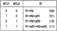
参见图8A和图8B,在磁RAM 700中,可变电阻元件MTJ1和MTJ2具有不同的电阻。如果第一可变电阻元件MTJ1的电阻具有最小值R1和最大值R1+ΔR1,而第二可变电阻元件MTJ2的电阻值具有最小值R2和最大值R2+ΔR2,那么根据写入第一和第二可变电阻元件MTJ1和MTJ2的数据磁RAM 700具有四个可能的电阻。8A and 8B, in the
磁RAM 700当两个可变电阻元件MTJ1和MTJ2都存储“0”时具有电阻R1+R2,当只有第一可变电阻元件MTJ1存储“1”时具有电阻R1+R2+ΔR1,当只有第二可变电阻元件MTJ2都存储“1”时具有电阻R1+R2+ΔR2,当两个可变电阻元件MTJ1和MTJ2都存储“1”时具有电阻R1+R2+ΔR1+ΔR2。The
当写入磁RAM 700的数据被读出时,施加恒定电流以产生相应于该电阻的电压并通过位线BL检测该产生的电压。When data written in the
图9是用于解释图7的磁RAM 700中的写入数据的表。FIG. 9 is a table for explaining write data in the
参见图7和图9,如果电流以右方向流过位线BL和第二电流供给线CSL2,由于产生的磁场的方向与第一和第二可变电阻元件MTJ1和MTJ2的固定铁磁层的磁化方向相同,所以第一和第二可变电阻元件MTJ1和MTJ2的总电阻降低,因此在第一和第二可变电阻元件MTJ1和MTJ2中写入数据“0”。Referring to FIGS. 7 and 9, if the current flows in the right direction through the bit line BL and the second current supply line CSL2, since the direction of the generated magnetic field is different from that of the fixed ferromagnetic layers of the first and second variable resistance elements MTJ1 and MTJ2 The magnetization directions are the same, so the total resistance of the first and second variable resistance elements MTJ1 and MTJ2 decreases, and thus data "0" is written in the first and second variable resistance elements MTJ1 and MTJ2.
如果电流以左方向流过位线BL和第二电流供给线CSL2,由于产生的磁场的方向与第一和第二可变电阻元件MTJ1和MTJ2的固定铁磁层的磁化方向相反,所以第一和第二可变电阻元件MTJ1和MTJ2的总电阻增大,因此在第一和第二可变电阻元件MTJ1和MTJ2中写入数据“1”。If current flows through the bit line BL and the second current supply line CSL2 in the left direction, since the direction of the generated magnetic field is opposite to the magnetization direction of the fixed ferromagnetic layers of the first and second variable resistance elements MTJ1 and MTJ2, the first The total resistance of the and second variable resistance elements MTJ1 and MTJ2 increases, and thus data "1" is written in the first and second variable resistance elements MTJ1 and MTJ2.
以这种方式,使用两个可变电阻元件MTJ1和MTJ2磁RAM 700可以存储2位数据。In this way, the
图10A是其中第一和第二可变电阻元件MTJ1和MTJ2的固定铁磁层的磁化方向与图7所示的不同的磁RAM 1000的示例图。FIG. 10A is an exemplary diagram of the
图10B是用于解释图10A的磁RAM 1000中的写入数据的表。FIG. 10B is a table for explaining write data in the
在图7的磁RAM 700中,第一和第二可变电阻元件MTJ1和MTJ2的固定铁磁层的磁化方向彼此相反。然而,在图10A的磁RAM 1000中,第一和第二可变电阻元件MTJ1和MTJ2的固定铁磁层的磁化方向是相同的。In the
相应地,通过流过位线BL和第二电流供给线CSL2的电流,图10B所示的数据被写入第一和第二可变电阻元件MTJ1和MTJ2。Accordingly, data shown in FIG. 10B is written in the first and second variable resistance elements MTJ1 and MTJ2 by the current flowing through the bit line BL and the second current supply line CSL2.
如果电流以右方向流过位线BL和第二电流供给线CSL2,由于产生的磁场方向与第一可变电阻元件MTJ1的固定铁磁层的磁化方向相同,所以第一可变电阻元件MTJ1的电阻降低。同样,由于产生的磁场的方向与第二可变电阻元件MTJ2的固定铁磁层的磁化方向相反,所以第二可变电阻元件MTJ2的电阻增大。因此,“0”被写入第一可变电阻元件MTJ1,而“1”被写入第二可变电阻元件MTJ2。If the current flows in the right direction through the bit line BL and the second current supply line CSL2, since the direction of the generated magnetic field is the same as the magnetization direction of the fixed ferromagnetic layer of the first variable resistance element MTJ1, the first variable resistance element MTJ1 The resistance decreases. Also, since the direction of the generated magnetic field is opposite to the magnetization direction of the fixed ferromagnetic layer of the second variable resistance element MTJ2, the resistance of the second variable resistance element MTJ2 increases. Therefore, "0" is written into the first variable resistance element MTJ1, and "1" is written into the second variable resistance element MTJ2.
如果电流以左方向流过位线BL和第二电流供给线CSL2,由于产生的磁场方向与第一可变电阻元件MTJ1的固定铁磁层的磁化方向相反,所以第一可变电阻元件MTJ1的电阻增大。同样,由于产生的磁场的方向与第二可变电阻元件MTJ2的固定铁磁层的磁化方向相同,所以第二可变电阻元件MTJ2的电阻降低。因此,“1”被写入第一可变电阻元件MTJ1,而“0”被写入第二可变电阻元件MTJ2。If the current flows in the left direction through the bit line BL and the second current supply line CSL2, since the direction of the generated magnetic field is opposite to the magnetization direction of the fixed ferromagnetic layer of the first variable resistance element MTJ1, the first variable resistance element MTJ1 The resistance increases. Also, since the direction of the generated magnetic field is the same as the magnetization direction of the fixed ferromagnetic layer of the second variable resistance element MTJ2, the resistance of the second variable resistance element MTJ2 decreases. Therefore, "1" is written into the first variable resistance element MTJ1, and "0" is written into the second variable resistance element MTJ2.
如果流过位线BL的电流方向和流过第二电流供给线CSL2的电流方向彼此相反,那么相同的数据可以被写入第一和第二可变电阻元件MTJ1和MTJ2。If the direction of current flowing through the bit line BL and the direction of current flowing through the second current supply line CSL2 are opposite to each other, the same data may be written in the first and second variable resistance elements MTJ1 and MTJ2.
为了图7中显示的磁RAM 700执行多位(例如n位)操作,提供2n-1个可变电阻元件。In order for the
根据本发明实施例的磁RAM包括形成在衬底上的访问晶体管、位线、交替堆叠在该访问晶体管上的数字线、布置在位线和数字线之间的多个可变电阻元件,其中该多个可变电阻元件在电气上彼此相连。A magnetic RAM according to an embodiment of the present invention includes an access transistor formed on a substrate, a bit line, a digit line alternately stacked on the access transistor, a plurality of variable resistance elements arranged between the bit line and the digit line, wherein The plurality of variable resistance elements are electrically connected to each other.
位线分别包括图3A和7的磁RAM 300和RAM 700中的位线BL和第二电流供给线CSL2,数字线分别包括图3A和7的磁RAM 300和RAM 700中的第一和第三电流供给线CSL1和CSL3。The bit lines include the bit line BL and the second current supply line CSL2 in the magnetic RAM 300 and
相应地,按照本发明的实施例的磁RAM可以具有与图3A和7的磁RAM300和RAM 700相似的结构,因此,它的详细描述被省略。Accordingly, the magnetic RAM according to the embodiment of the present invention may have a structure similar to the magnetic RAM 300 and
虽然本发明参考其示例性实施例被特别地显示和描述,但本领域技术人员可以理解,可以进行各种形式和细节上的改变和描述而不脱离本发明的精神和范围。Although the present invention has been particularly shown and described with reference to exemplary embodiments thereof, it will be understood by those skilled in the art that various changes and descriptions may be made in form and detail without departing from the spirit and scope of the invention.
本申请要求在韩国知识产权局申请的申请日为2004年10月28日、申请号为10-2004-0086556的韩国专利的优先权,将该申请的公开内容全部引用结合于此。This application claims the priority of Korean Patent Application No. 10-2004-0086556 filed at the Korean Intellectual Property Office on October 28, 2004, the disclosure of which is incorporated herein by reference in its entirety.
Claims (30)
Translated fromChineseApplications Claiming Priority (2)
| Application Number | Priority Date | Filing Date | Title |
|---|---|---|---|
| KR1020040086556AKR100604913B1 (en) | 2004-10-28 | 2004-10-28 | Magnetic RAM with Multi-Bit Cell Array Structure |
| KR86556/04 | 2004-10-28 |
Publications (2)
| Publication Number | Publication Date |
|---|---|
| CN1822226A CN1822226A (en) | 2006-08-23 |
| CN100573713Ctrue CN100573713C (en) | 2009-12-23 |
Family
ID=35258828
Family Applications (1)
| Application Number | Title | Priority Date | Filing Date |
|---|---|---|---|
| CNB2005100034564AActiveCN100573713C (en) | 2004-10-28 | 2005-10-28 | Magnetoresistive RAM with multi-bit unit array structure |
Country Status (5)
| Country | Link |
|---|---|
| US (1) | US7463509B2 (en) |
| EP (1) | EP1653516A3 (en) |
| JP (1) | JP2006140468A (en) |
| KR (1) | KR100604913B1 (en) |
| CN (1) | CN100573713C (en) |
Families Citing this family (28)
| Publication number | Priority date | Publication date | Assignee | Title |
|---|---|---|---|---|
| US7272028B2 (en) | 2005-05-27 | 2007-09-18 | Infineon Technologies Ag | MRAM cell with split conductive lines |
| KR100695171B1 (en)* | 2006-02-23 | 2007-03-14 | 삼성전자주식회사 | Magnetic memory device using magnetic domain movement |
| KR100850508B1 (en)* | 2006-08-04 | 2008-08-05 | 삼성전자주식회사 | NAND FLASH Memory Device With 3-Dimensionally Arranged Memory Cell Transistors |
| US7697316B2 (en)* | 2006-12-07 | 2010-04-13 | Macronix International Co., Ltd. | Multi-level cell resistance random access memory with metal oxides |
| KR100837412B1 (en)* | 2006-12-12 | 2008-06-12 | 삼성전자주식회사 | Multi Stack Memory Devices |
| KR100814108B1 (en)* | 2006-12-12 | 2008-03-14 | 인하대학교 산학협력단 | Logic circuit using magnetic tunnel junction |
| KR100996191B1 (en) | 2007-04-25 | 2010-11-24 | 주식회사 하이닉스반도체 | Nonvolatile Memory Device and Manufacturing Method Thereof |
| KR101258268B1 (en)* | 2007-07-26 | 2013-04-25 | 삼성전자주식회사 | NAND-type resistive memory cell strings of a non-volatile memory device and methods of fabricating the same |
| KR100858688B1 (en)* | 2007-12-06 | 2008-09-16 | 한양대학교 산학협력단 | Nonvolatile Memory and How to Read It |
| FR2925747B1 (en)* | 2007-12-21 | 2010-04-09 | Commissariat Energie Atomique | MAGNETIC MEMORY WITH THERMALLY ASSISTED WRITING |
| US7919794B2 (en)* | 2008-01-08 | 2011-04-05 | Qualcomm, Incorporated | Memory cell and method of forming a magnetic tunnel junction (MTJ) of a memory cell |
| US7804710B2 (en)* | 2008-03-31 | 2010-09-28 | International Business Machines Corporation | Multi-layer magnetic random access memory using spin-torque magnetic tunnel junctions and method for write state of the multi-layer magnetic random access memory |
| US8482966B2 (en)* | 2008-09-24 | 2013-07-09 | Qualcomm Incorporated | Magnetic element utilizing protective sidewall passivation |
| JP2010251529A (en)* | 2009-04-16 | 2010-11-04 | Sony Corp | Semiconductor memory device and manufacturing method thereof |
| US8411494B2 (en) | 2009-07-21 | 2013-04-02 | Alexander Mikhailovich Shukh | Three-dimensional magnetic random access memory with high speed writing |
| US8331141B2 (en) | 2009-08-05 | 2012-12-11 | Alexander Mikhailovich Shukh | Multibit cell of magnetic random access memory with perpendicular magnetization |
| US8988934B2 (en) | 2010-07-27 | 2015-03-24 | Alexander Mikhailovich Shukh | Multibit cell of magnetic random access memory with perpendicular magnetization |
| EP2466586B1 (en)* | 2010-12-16 | 2016-03-02 | Crocus Technology | Multibit magnetic random access memory cell with improved read margin |
| JP5501277B2 (en)* | 2011-03-24 | 2014-05-21 | 株式会社東芝 | Nonvolatile memory device |
| JP5537501B2 (en)* | 2011-06-09 | 2014-07-02 | 株式会社東芝 | Semiconductor memory device and manufacturing method thereof |
| US8675390B2 (en) | 2011-10-21 | 2014-03-18 | Qualcomm Incorporated | System and method for MRAM having controlled averagable and isolatable voltage reference |
| US9203015B2 (en) | 2013-03-22 | 2015-12-01 | Hisanori Aikawa | Magnetic storage device |
| US8987846B2 (en)* | 2013-03-22 | 2015-03-24 | Yoshinori Kumura | Magnetic memory and manufacturing method thereof |
| CN103761987A (en)* | 2014-01-08 | 2014-04-30 | 华中科技大学 | RRAM (resistive random access memory)-based multi-bit storage structure and read-write operation method for same |
| US9747967B2 (en) | 2014-09-26 | 2017-08-29 | Intel Corporation | Magnetic field-assisted memory operation |
| JP2017059740A (en)* | 2015-09-18 | 2017-03-23 | 富士通株式会社 | Magnetic tunnel junction element and semiconductor memory device |
| JP2019160368A (en) | 2018-03-13 | 2019-09-19 | 東芝メモリ株式会社 | Semiconductor storage device |
| CN110277115B (en)* | 2019-06-24 | 2021-01-01 | 中国科学院微电子研究所 | Magnetic tunnel junction-based memory, read-write method and fabrication method thereof |
Family Cites Families (20)
| Publication number | Priority date | Publication date | Assignee | Title |
|---|---|---|---|---|
| US5748519A (en)* | 1996-12-13 | 1998-05-05 | Motorola, Inc. | Method of selecting a memory cell in a magnetic random access memory device |
| JP3913971B2 (en) | 1999-12-16 | 2007-05-09 | 株式会社東芝 | Magnetic memory device |
| JP2001217398A (en)* | 2000-02-03 | 2001-08-10 | Rohm Co Ltd | Storage device using ferromagnetic tunnel junction element |
| JP2002230965A (en)* | 2001-01-24 | 2002-08-16 | Internatl Business Mach Corp <Ibm> | Non-volatile memory device |
| JP3892736B2 (en) | 2001-03-29 | 2007-03-14 | 株式会社東芝 | Semiconductor memory device |
| EP1398835A4 (en)* | 2001-06-19 | 2006-03-29 | Matsushita Electric Industrial Co Ltd | MAGNETIC MEMORY AND METHOD FOR ITS CONTROL AND MAGNETIC MEMORY DEVICE THEREWITH |
| JP3527230B2 (en) | 2001-06-19 | 2004-05-17 | 松下電器産業株式会社 | Driving method of magnetic memory |
| JP3830785B2 (en) | 2001-08-10 | 2006-10-11 | 田中貴金属工業株式会社 | Method for producing organoruthenium compound for CVD and organoruthenium compound for CVD |
| JP2003133528A (en) | 2001-10-24 | 2003-05-09 | Sony Corp | Information memory, information writing method and manufacturing method therefor |
| EP1321941B1 (en) | 2001-12-21 | 2005-08-17 | Kabushiki Kaisha Toshiba | Magnetic random access memory with stacked memory cells |
| US6795334B2 (en)* | 2001-12-21 | 2004-09-21 | Kabushiki Kaisha Toshiba | Magnetic random access memory |
| KR100457159B1 (en)* | 2001-12-26 | 2004-11-16 | 주식회사 하이닉스반도체 | Magnetic random access memory |
| JP3875568B2 (en)* | 2002-02-05 | 2007-01-31 | 株式会社東芝 | Semiconductor device and manufacturing method thereof |
| JP2003309251A (en)* | 2002-04-18 | 2003-10-31 | Toshiba Corp | Magnetic random access memory |
| US7042749B2 (en) | 2002-05-16 | 2006-05-09 | Micron Technology, Inc. | Stacked 1T-nmemory cell structure |
| JP4080795B2 (en) | 2002-06-26 | 2008-04-23 | 株式会社東芝 | Magnetic memory device |
| US20050195673A1 (en)* | 2002-07-15 | 2005-09-08 | Yoshiaki Asao | Magnetic random access memory having memory cells configured by use of tunneling magnetoresistive elements |
| US7196882B2 (en)* | 2002-07-23 | 2007-03-27 | Micron Technology, Inc. | Magnetic tunnel junction device and its method of fabrication |
| US6925003B2 (en)* | 2003-09-08 | 2005-08-02 | Hewlett-Packard Development Company, L.P. | Magnetic memory cell structure |
| US20050073878A1 (en)* | 2003-10-03 | 2005-04-07 | Taiwan Semiconductor Manufacturing Co., Ltd. | Multi-sensing level MRAM structure with different magnetoresistance ratios |
- 2004
- 2004-10-28KRKR1020040086556Apatent/KR100604913B1/ennot_activeExpired - Lifetime
- 2005
- 2005-10-27EPEP05023489Apatent/EP1653516A3/ennot_activeWithdrawn
- 2005-10-27USUS11/260,602patent/US7463509B2/enactiveActive
- 2005-10-27JPJP2005313040Apatent/JP2006140468A/enactivePending
- 2005-10-28CNCNB2005100034564Apatent/CN100573713C/enactiveActive
Also Published As
| Publication number | Publication date |
|---|---|
| CN1822226A (en) | 2006-08-23 |
| KR20060037562A (en) | 2006-05-03 |
| US20060092690A1 (en) | 2006-05-04 |
| EP1653516A3 (en) | 2007-10-10 |
| EP1653516A2 (en) | 2006-05-03 |
| JP2006140468A (en) | 2006-06-01 |
| KR100604913B1 (en) | 2006-07-28 |
| US7463509B2 (en) | 2008-12-09 |
Similar Documents
| Publication | Publication Date | Title |
|---|---|---|
| CN100573713C (en) | Magnetoresistive RAM with multi-bit unit array structure | |
| CN100466093C (en) | Magnetoresistive memory devices with double tunnel junctions | |
| US7286429B1 (en) | High speed sensing amplifier for an MRAM cell | |
| US8098513B2 (en) | Memory array with read reference voltage cells | |
| US5640343A (en) | Magnetic memory array using magnetic tunnel junction devices in the memory cells | |
| US7643332B2 (en) | MRAM cell using multiple axes magnetization and method of operation | |
| US7835210B2 (en) | Magnetic random access memory and data read method of the same | |
| US7961509B2 (en) | Spin-transfer torque memory self-reference read and write assist methods | |
| US7411815B2 (en) | Memory write circuit | |
| US7940592B2 (en) | Spin-torque bit cell with unpinned reference layer and unidirectional write current | |
| US20060152973A1 (en) | Multi-sensing level MRAM structure with different magneto-resistance ratios | |
| JP2002533863A (en) | Magnetic random access memory with reference memory array | |
| US6754097B2 (en) | Read operations on multi-bit memory cells in resistive cross point arrays | |
| US8526215B2 (en) | Spatial correlation of reference cells in resistive memory array | |
| US20060039183A1 (en) | Multi-sensing level MRAM structures | |
| US7050326B2 (en) | Magnetic memory device with current carrying reference layer | |
| US6980466B2 (en) | Soft-reference four conductor magnetic memory storage device | |
| JP2003188359A (en) | Magneto-resistive device including magnetically soft synthetic ferrimagnet reference layer | |
| JP4492052B2 (en) | Magnetic storage cell and magnetic memory device | |
| US7391641B2 (en) | Multi-layered magnetic memory structures | |
| US7457153B1 (en) | Integrated circuit memory devices having magnetic memory cells therein that utilize dual-ferromagnetic data layers |
Legal Events
| Date | Code | Title | Description |
|---|---|---|---|
| C06 | Publication | ||
| PB01 | Publication | ||
| C10 | Entry into substantive examination | ||
| SE01 | Entry into force of request for substantive examination | ||
| C14 | Grant of patent or utility model | ||
| GR01 | Patent grant |