CN100565882C - Method, semi-conductor device manufacturing method - Google Patents
Method, semi-conductor device manufacturing methodDownload PDFInfo
- Publication number
- CN100565882C CN100565882CCNB018004350ACN01800435ACN100565882CCN 100565882 CCN100565882 CCN 100565882CCN B018004350 ACNB018004350 ACN B018004350ACN 01800435 ACN01800435 ACN 01800435ACN 100565882 CCN100565882 CCN 100565882C
- Authority
- CN
- China
- Prior art keywords
- gate
- layer
- gate structure
- semiconductor body
- access
- Prior art date
- Legal status (The legal status is an assumption and is not a legal conclusion. Google has not performed a legal analysis and makes no representation as to the accuracy of the status listed.)
- Expired - Fee Related
Links
Images


Classifications
- H—ELECTRICITY
- H10—SEMICONDUCTOR DEVICES; ELECTRIC SOLID-STATE DEVICES NOT OTHERWISE PROVIDED FOR
- H10B—ELECTRONIC MEMORY DEVICES
- H10B43/00—EEPROM devices comprising charge-trapping gate insulators
- H10B43/30—EEPROM devices comprising charge-trapping gate insulators characterised by the memory core region
- H—ELECTRICITY
- H10—SEMICONDUCTOR DEVICES; ELECTRIC SOLID-STATE DEVICES NOT OTHERWISE PROVIDED FOR
- H10B—ELECTRONIC MEMORY DEVICES
- H10B41/00—Electrically erasable-and-programmable ROM [EEPROM] devices comprising floating gates
- H10B41/30—Electrically erasable-and-programmable ROM [EEPROM] devices comprising floating gates characterised by the memory core region
- H—ELECTRICITY
- H10—SEMICONDUCTOR DEVICES; ELECTRIC SOLID-STATE DEVICES NOT OTHERWISE PROVIDED FOR
- H10B—ELECTRONIC MEMORY DEVICES
- H10B69/00—Erasable-and-programmable ROM [EPROM] devices not provided for in groups H10B41/00 - H10B63/00, e.g. ultraviolet erasable-and-programmable ROM [UVEPROM] devices
- H—ELECTRICITY
- H10—SEMICONDUCTOR DEVICES; ELECTRIC SOLID-STATE DEVICES NOT OTHERWISE PROVIDED FOR
- H10D—INORGANIC ELECTRIC SEMICONDUCTOR DEVICES
- H10D30/00—Field-effect transistors [FET]
- H10D30/01—Manufacture or treatment
- H10D30/021—Manufacture or treatment of FETs having insulated gates [IGFET]
- H10D30/0411—Manufacture or treatment of FETs having insulated gates [IGFET] of FETs having floating gates
- H—ELECTRICITY
- H10—SEMICONDUCTOR DEVICES; ELECTRIC SOLID-STATE DEVICES NOT OTHERWISE PROVIDED FOR
- H10D—INORGANIC ELECTRIC SEMICONDUCTOR DEVICES
- H10D30/00—Field-effect transistors [FET]
- H10D30/01—Manufacture or treatment
- H10D30/021—Manufacture or treatment of FETs having insulated gates [IGFET]
- H10D30/0413—Manufacture or treatment of FETs having insulated gates [IGFET] of FETs having charge-trapping gate insulators, e.g. MNOS transistors
- H—ELECTRICITY
- H10—SEMICONDUCTOR DEVICES; ELECTRIC SOLID-STATE DEVICES NOT OTHERWISE PROVIDED FOR
- H10D—INORGANIC ELECTRIC SEMICONDUCTOR DEVICES
- H10D30/00—Field-effect transistors [FET]
- H10D30/60—Insulated-gate field-effect transistors [IGFET]
- H10D30/68—Floating-gate IGFETs
- H10D30/6891—Floating-gate IGFETs characterised by the shapes, relative sizes or dispositions of the floating gate electrode
- H10D30/6892—Floating-gate IGFETs characterised by the shapes, relative sizes or dispositions of the floating gate electrode having at least one additional gate other than the floating gate and the control gate, e.g. program gate, erase gate or select gate
Landscapes
- Semiconductor Memories (AREA)
- Non-Volatile Memory (AREA)
- Electrodes Of Semiconductors (AREA)
Abstract
Description
Translated fromChinese技术领域technical field
本发明涉及一种半导体器件,在其半导体本体的表面上提供有非易失性存储器元件。本发明还涉及制造一种半导体器件的方法,在所述半导体器件的半导体本体的表面含有一个非易失性存储器元件。The invention relates to a semiconductor device provided on the surface of its semiconductor body with a non-volatile memory element. The invention also relates to a method of manufacturing a semiconductor device comprising a non-volatile memory element at the surface of a semiconductor body of the semiconductor device.
背景技术Background technique
这种半导体器件见于美国专利US 5,607,871。在已知的半导体器件中,非易失性存储器元件包括源和漏,以及与包含控制栅的栅结构电绝缘的一个存取栅。上述栅结构与半导体本体通过栅极电介质层电绝缘,带有一个用作电荷存储区的浮栅,其中以电荷的形式存储数据。存取栅具有基本上平行于半导体本体的表面延伸的大致平坦的表面部分。存取栅是通过构图与该栅结构和相邻的栅结构重叠的多晶硅层形成的,并伸展超过栅结构的最外面的侧壁。在栅结构之间,构图的多晶硅层位于局域地形成在半导体本体中的漏极之上,源极形成在半导体本体中,与构图后的多晶硅层对准。Such semiconductor devices are described in US Patent No. 5,607,871. In known semiconductor devices, a non-volatile memory element includes a source and a drain, and an access gate electrically insulated from a gate structure including a control gate. The aforementioned gate structure is electrically insulated from the semiconductor body by a gate dielectric layer, with a floating gate serving as a charge storage area, in which data is stored in the form of charge. The access gate has a substantially planar surface portion extending substantially parallel to the surface of the semiconductor body. The access gate is formed by patterning a polysilicon layer that overlaps the gate structure and adjacent gate structures and extends beyond the outermost sidewalls of the gate structures. Between the gate structures, a patterned polysilicon layer overlies a drain locally formed in the semiconductor body, and a source is formed in the semiconductor body in alignment with the patterned polysilicon layer.
已知的半导体器件的缺点是,由于在栅结构区域和位于这些区域上的多晶硅层的大的拓扑结构,多晶硅层的光刻构图很困难。当在多晶硅层上形成的光刻胶层被曝光以形成光刻图案时,在多晶硅层的表面上光线被反射到倾斜的方向上。结果使光刻图案变形,导致多晶硅层构图的精确性很差。当构图多晶硅层位于漏极之上时,已知半导体器件的另一缺点是在一个单独的步骤里不能同时形成源极和漏极,在存储器元件的工作过程中构图的多晶硅层和漏极之间会发生串扰。A disadvantage of the known semiconductor components is that photolithographic patterning of the polysilicon layer is difficult due to the large topography in the gate structure regions and the polysilicon layer lying on these regions. When the photoresist layer formed on the polysilicon layer is exposed to form a photoresist pattern, light is reflected in oblique directions on the surface of the polysilicon layer. As a result, the photolithographic pattern is distorted, resulting in poor patterning accuracy of the polysilicon layer. Another disadvantage of known semiconductor devices is that the source and drain cannot be formed simultaneously in a single step when the patterned polysilicon layer is located above the drain, between the patterned polysilicon layer and the drain during operation of the memory element. crosstalk will occur.
上述非易失性存储器元件包括一个存取晶体管和一个浮栅晶体管,在浮栅晶体管中包括一个可以以电荷形式存储数据的浮栅。如本领域所公知的,可以使用一个所谓电荷陷阱(rapping)晶体管来代替上述的浮栅晶体管。这种电荷陷阱管包括一个通过栅极电介质层与半导体本体绝缘的控制栅,栅极电介质层包括可以存储电荷的相互隔开的陷阱中心。在这种电荷陷阱晶体管中,电荷不但能只在沟道的全部长度范围内存在,还可以只在沟道的源极侧或漏极侧存在。由于在读取过程中可以分辨这些不同的情况,每个存储器元件可以存储2个比特。The above-mentioned nonvolatile memory element includes an access transistor and a floating gate transistor including a floating gate capable of storing data in the form of electric charges. As known in the art, a so-called charge trapping transistor can be used instead of the floating gate transistor described above. The charge trapping transistor comprises a control gate insulated from the semiconductor body by a gate dielectric layer comprising mutually spaced trap centers capable of storing charges. In such a charge-trap transistor, charge can exist not only over the entire length of the channel, but also only on the source or drain side of the channel. Since these different cases can be resolved during read, each memory element can store 2 bits.
不论象上述已知的半导体器件那样将浮栅用于存储电荷,还是在栅极介质层中包括相互隔开的陷阱中心,都包括上述的缺点。这些缺点也存在于电荷陷阱晶体管中。Whether a floating gate is used to store charge as in the known semiconductor devices described above, or trap centers spaced apart from each other are included in the gate dielectric layer, the above-mentioned disadvantages are involved. These disadvantages also exist in charge trap transistors.
上述半导体器件的制造方法描述于美国专利US5,607,871。在已知的方法中,在施加导电层即多晶硅层之前,在半导体本体上形成位于一个栅结构和相邻的栅结构之间的漏极。然后构图多晶硅层,使其与上述栅结构和相邻的栅结构重叠,并延伸超过这些栅结构的最外面的侧壁。在构图多晶硅后,在半导体本体上形成与构图后的多晶硅对准的源极。A method of manufacturing the above semiconductor device is described in US Pat. No. 5,607,871. In known methods, the drain between one gate structure and the adjacent gate structure is formed on the semiconductor body before the conductive layer, ie the polysilicon layer, is applied. The polysilicon layer is then patterned so as to overlap the aforementioned gate structure and adjacent gate structures and extend beyond the outermost sidewalls of these gate structures. After patterning the polysilicon, a source electrode aligned with the patterned polysilicon is formed on the semiconductor body.
这种方法的缺点在于,由于在栅结构位置和施加在栅结构上的多晶硅层的大的拓扑结构,多晶硅层的光刻构图很困难。当形成在多晶硅层上的光刻胶被曝光以形成光刻图案时,在多晶硅层的表面上光被反射到倾斜的方向上。结果光刻图案变形,导致构图光刻胶层的精确性很差。由于构图的多晶硅层位于漏极上,上述方法的另一缺点是不能在一个单独的步骤里形成源极和漏极,且在存储器元件的操作过程中在构图的多晶硅层和漏极之间存在串扰。A disadvantage of this method is that photolithographic patterning of the polysilicon layer is difficult due to the large topology of the polysilicon layer at the gate structure location and applied on the gate structure. When the photoresist formed on the polysilicon layer is exposed to form a photoresist pattern, light is reflected in oblique directions on the surface of the polysilicon layer. As a result, the photolithographic pattern is distorted, resulting in poor precision in patterning the photoresist layer. Another disadvantage of the above method is that the source and drain cannot be formed in a single step due to the patterned polysilicon layer on the drain, and there is a gap between the patterned polysilicon layer and the drain during operation of the memory element. crosstalk.
上述的制造带有浮栅晶体管的半导体器件的方法的缺点也发生在制造具有电荷陷阱晶体管的半导体器件的方法中。The above-described disadvantages of the method of manufacturing a semiconductor device with floating gate transistors also occur in the method of manufacturing a semiconductor device with charge trap transistors.
发明内容Contents of the invention
因此本发明的目的是提供一种制造带有非易失性存储器元件的半导体器件,该方法能更容易和更准确地实施并能消除操作过程中,的上述串扰问题。It is therefore an object of the present invention to provide a method of manufacturing semiconductor devices with non-volatile memory elements which can be carried out more easily and accurately and which eliminates the above-mentioned crosstalk problems during operation.
因此本发明的另一个目的是提供一种带有存储器元件的半导体器件,其中能更容易地和更精确地制造所述存储器元件,且能消除上述的操作中的串扰问题。It is therefore another object of the present invention to provide a semiconductor device with a memory element which can be manufactured more easily and precisely and which eliminates the above-mentioned crosstalk problem in operation.
根据本发明,提供了一种制造半导体器件的方法,在所述半导体器件的半导体本体的表面具有一个非易失性存储器元件,通过该方法在半导体本体的表面上形成包含控制栅的栅结构,所述栅结构与半导体本体通过栅极介质层绝缘,栅极介质层带有能以电荷形式存储数据的电荷存储区,之后施加一导电层,其厚度为使得挨着栅结构的导电层的上表面位于与栅结构的上表面部分相同的高度处,或比之更高,通过平面化处理去除导电层的一部分厚度直到暴露出栅结构为止,之后构图导电层,同时使用一个掩膜以形成块状存取栅,所述掩膜从栅结构延伸到毗邻栅结构的导电层的一个区域之上。According to the invention, there is provided a method of manufacturing a semiconductor device having a non-volatile memory element on the surface of a semiconductor body, by which method a gate structure comprising a control gate is formed on the surface of the semiconductor body, The gate structure is insulated from the semiconductor body by a gate dielectric layer with a charge storage area capable of storing data in the form of charges, and then a conductive layer is applied with a thickness such that it is adjacent to the top of the conductive layer of the gate structure. The surface is at the same height as, or higher than, the upper surface portion of the gate structure, a portion of the thickness of the conductive layer is removed by planarization until the gate structure is exposed, and the conductive layer is patterned while using a mask to form the block The mask extends from the gate structure over a region of the conductive layer adjacent to the gate structure.
其中掩膜通过淀积光刻胶层来施加,所述光刻胶层通过曝光来构图。在形成块状存取栅之后,在半导体本体的表面上形成源和漏,包括以下步骤:在使用栅结构和存取栅作为掩膜的同时,通过自对准注入在半导体本体的表面内提供与半导体本体的导电类型相反导电类型的源和漏延伸区;在栅结构和存取栅的两个侧壁上均形成侧壁间隔层;使用栅结构、存取栅和侧壁间隔层作为掩膜,通过自对准注入在侧壁间隔层的相对侧壁上提供源和漏。Where the mask is applied by depositing a photoresist layer which is patterned by exposure to light. After forming the bulk access gate, the source and drain are formed on the surface of the semiconductor body, comprising the steps of: while using the gate structure and the access gate as a mask, providing in the surface of the semiconductor body by self-aligned implantation Source and drain extension regions of a conductivity type opposite to that of the semiconductor body; sidewall spacers are formed on both sidewalls of the gate structure and the access gate; using the gate structure, the access gate and the sidewall spacers as masks film, providing sources and drains on opposite sidewalls of the sidewall spacers by self-aligned implants.
其中栅结构带有一个绝缘层作为最上面的层,所述绝缘层由对平面化处理比导电层所用的材料更具抵抗力的材料组成。其中施加氧化硅或氮化硅作为绝缘层,且通过淀积一层多晶硅作为导电层。In this case, the gate structure has, as the uppermost layer, an insulating layer consisting of a material which is more resistant to planarization than the material used for the conductive layer. Among them, silicon oxide or silicon nitride is applied as an insulating layer, and a layer of polysilicon is deposited as a conductive layer.
其中利用化学机械抛光(CMP)作为平面化处理的方法。Among them, chemical mechanical polishing (CMP) is used as a planarization method.
根据本发明的方法,在导电层上形成有掩膜的时候,导电层具有基本平坦的表面。因此当通过淀积光测胶层施加掩膜时,通过曝光来构图光刻胶层,光不会在导电层的表面上反射到倾斜的方向。因此能以更高的精确性形成存取栅。此外,使用栅结构和存取栅作为掩膜可以在一个单独的步骤里形成源极和漏极。依此方式,漏极和(由导电层形成的)存取栅之间的串扰可以被消除。According to the method of the present invention, when the mask is formed on the conductive layer, the conductive layer has a substantially flat surface. Therefore, when a mask is applied by depositing a photoresist layer, the photoresist layer is patterned by exposure, and light is not reflected to oblique directions on the surface of the conductive layer. Therefore, the access gate can be formed with higher precision. In addition, the source and drain can be formed in a single step using the gate structure and the access gate as a mask. In this way, crosstalk between the drain and the access gate (formed of the conductive layer) can be eliminated.
电荷存储区可以由例如浮栅形成。在另一个实施例中,电荷存储区中含有相互隔开的陷阱中心。例如,带有相互隔开的陷阱中心的栅极电介质层可以是含有杂质的二氧化硅层,杂质可以是分布在其中的金属粒子,杂质形成陷阱中心。然而,更普遍的方式是使用包括两层不同材料的栅介质层,它形成提供相互隔开的陷阱中心的边界层。为了增大与标准CMOS工艺的兼容性,双层的栅介质层优选地由一层二氧化硅层和一层氮化硅层构成。The charge storage region may be formed of, for example, a floating gate. In another embodiment, the charge storage region contains trap centers spaced apart from each other. For example, the gate dielectric layer with spaced apart trap centers may be a silicon dioxide layer containing impurities, which may be metal particles distributed therein, that form the trap centers. However, a more common approach is to use a gate dielectric layer comprising two layers of different materials, which form a boundary layer providing trap centers separated from each other. In order to increase the compatibility with the standard CMOS process, the double-layer gate dielectric layer is preferably composed of a silicon dioxide layer and a silicon nitride layer.
在根据本发明方法的半导体器件的另一个实施例中,存取栅的基本平坦的表面部分位于与栅结构的上表面部分基本相同高度的地方。因此,存取栅和栅结构的组合结构基本是平坦的。In a further embodiment of the semiconductor device according to the method of the invention, the substantially planar surface portion of the access gate is located at substantially the same height as the upper surface portion of the gate structure. Thus, the combined structure of the access gate and gate structure is substantially planar.
在包含一个存取栅的非易失性存储器元件中,该存储器元件也称为双晶体管元件(2T),存取栅优选地位于邻近源极的栅结构的一侧。如果存取栅位于源极侧,则用于开关的编程电压小于当存取栅位于漏极侧的用于开关所需的编程电压,因此前一种存取晶体管可以具有更薄的栅极电介质层。In a non-volatile memory element comprising one access gate, also known as a two-transistor element (2T), the access gate is preferably located on the side of the gate structure adjacent to the source. If the access gate is on the source side, the programming voltage for switching is less than that required for switching when the access gate is on the drain side, so the former access transistor can have a thinner gate dielectric layer.
本发明的这些和其它方面可以从后面的优选实施方案详述和附图中得知。These and other aspects of the invention can be gleaned from the following detailed description of the preferred embodiments and accompanying drawings.
附图说明Description of drawings
图1表示根据本发明的相邻的非易失性存储器元件的第一实施例的示意剖视图。Figure 1 shows a schematic cross-sectional view of a first embodiment of adjacent non-volatile memory elements according to the invention.
图2-7表示使用本发明的方法制造图1所示的相邻的非易失性存储器元件制造过程的各个阶段的剖视图。2-7 show cross-sectional views of various stages in the fabrication of adjacent nonvolatile memory elements shown in FIG. 1 using the method of the present invention.
图8表示根据本发明的相邻的非易失性存储器元件的第二实施例的示意剖视图。Fig. 8 shows a schematic cross-sectional view of a second embodiment of adjacent non-volatile memory elements according to the invention.
图9-14表示使用本发明的方法制造图8所示的相邻的非易失性存储器元件的各个阶段的剖视图。9-14 show cross-sectional views of various stages in the fabrication of adjacent non-volatile memory elements shown in FIG. 8 using the method of the present invention.
具体实施方式Detailed ways
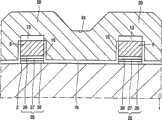
图1表示第一导类型的半导体本体1,在本例中,例如是p型的硅。在半导体本体1的表面2上提供有包括相反的第二导电类型的源3和漏4的非易失性存储器元件,第二导电类型在本例中为n型。源3和漏4在本例中带有延伸区5。在存储器元件的延伸的源3.5和延伸的漏4.5之间,在半导体本体1的表面2上形成有浮栅晶体管6和存取晶体管7。浮栅晶体管6包括栅结构8,栅结构8又包含控制栅9。在栅结构8和半导体本体1之间,提供有导电材料层10,该导电材料层10的所有侧壁由电绝缘材料环绕,形成浮栅。浮栅10用作电荷存储区,以电荷形式存储数据。浮栅10和控制栅9可以由例如掺杂磷的多晶硅组成。或者,非晶硅或SiXGe1-X可以用作浮栅10和控制栅9,其中X表示硅的含量,在0.6和1之间。浮栅10和半导体本体1之间通过浮栅电介质层11绝缘,和控制栅9之间通过栅极间介质层12绝缘。浮栅电介质层11和栅极间介质层12可以由例如二氧化硅组成。或者浮栅介质层11和栅极间介质层12可以由介电常数明显地硅高的介质材料组成,例如氧化钽,氧化铝或氮化硅。其它适用于栅极间介质材料12的介质材料是例如,氮氧化硅(SiON)和氧化硅与氮化硅的夹层结构(ONO)。栅结构8包括绝缘层13作为最上层,绝缘层13优选地由氮化硅或氧化硅组成。存取晶体管7具有存取栅14,它与半导体本体1通过栅极电介质层15绝缘。存取栅14可以由例如掺杂磷的多晶硅、非晶硅或SiXGe1-X构成,其中X表示硅的含量,在0.6和1之间。栅极电介质层15可以由例如氧化硅或者介电常数明显高于氧化硅的介质材料如氧化钽、氧化铝或氮化硅构成。存取晶体管7和存取栅14通过例如为氧化硅或氮化硅的绝缘材料16与栅结构8绝缘。存取栅14具有挨着栅结构8放置的块状结构,没有与栅结构8重叠的部分。存取栅14具有与半导体本体1的表面2基本平行地延伸的基本平坦的表面部分17。存取栅14的基本平坦的表面部分17、源3和漏4带有金属硅化物18,例如是硅化钛的低阻欧姆接触。在本例中,存取栅14的基本平坦的表面部分17与栅结构8的上表面部分23位于基本相同的高度。FIG. 1 shows a
在上述非易失性存储器元件中,存取栅14位于邻近源3的栅结构8的一侧。显然,存取栅14可以位于邻近漏4的栅结构8的一侧。或者非易失性存储器元件包含两个存取栅,而不是一个,这两个存取栅位于栅结构8的两侧。带有两个存取晶体管的非易失性存储器元件通常称为三晶体管元件(3T)。非易失性存储器元件可以是存储器元件阵列的一部分,所述阵列嵌在CMDS或BIMOS集成电路中,或者是单独的非易失性存储器的一部分。In the above-mentioned nonvolatile memory element, the
图2至7表示使用根据本发明的方法制造图1的非易失性存储器元件的各个阶段的示意性剖视图。2 to 7 show schematic cross-sectional views of various stages in the manufacture of the non-volatile memory element of FIG. 1 using the method according to the invention.
制造过程从第一导电类型的半导体本体1开始(图2),它在本例中是p型的硅本体。半导体本体1的表面2上具有一个堆栈,包括:浮栅介质层11、浮栅10、栅极间介质层12和栅结构8,栅结构8已包括控制栅9和绝缘层13,绝缘层13是栅结构8的最上面的层。该堆栈依常规方式形成,即淀积不同的层,然后构图这些层以形成堆栈。The manufacturing process starts with a
在下一个步骤中(图3),半导体本体1的表面2的暴露部分提供有介质层19,它在以后的步骤中形成存取晶体管7的栅极介质层15。然后,栅结构8的侧壁部分用绝缘材料16盖覆以与存取栅14绝缘,存了栅14在以后的工艺阶段形成。然后,施加导电层14,其厚度使得与栅结构8相邻的导电层20的上表面24位于与栅结构8的上表面部分23相同的高度,或比之更高。In a next step ( FIG. 3 ), exposed parts of the
参考图4,通过平面化处理去除导电层20的一部分厚度,直到露出栅结构8。为了准确地停止平面化处理,栅结构8优选地包括一个绝缘层3作为它的最上层,绝缘层13由对平面化处理的耐受性比导电层20所用的材料更高的材料组成。绝缘层3用作平面化处理的停止层。如果施加多晶硅用作导电层20,绝缘层13优选地由氧化硅或氮化硅组成。化学机械抛光(CMP)优选地用于去除导电层20的一部分厚度。为此可以使用比较经济的浆料。Referring to FIG. 4 , a part of the thickness of the
在下一步骤(图5),构图导电层20,使用掩膜21以形成存取晶体管7的存取栅14,掩膜21从栅结构8延伸到覆盖毗邻栅结构8的导电层20的一部分。优选通过光刻来构图导电层20。为此,光刻胶淀积在导电层20上,光刻胶层被曝光构图以形成掩膜21,之后去除导电层20的未被掩蔽的部分。由于在通过曝光构图光刻胶层时,导电层20的表面是基本平坦的,所以光不会被导电层20的表面反射到倾斜的方向上。因此能以较大的准确性表成存取栅14(图6),存取栅14与半导体本体1通过栅极介质层15绝缘,栅极介质层由介质层19形成。在形成存取栅14之后,半导体本体1的表面2上形成相反的第2导电类型(在本例中是n型)的源/漏区5,使用栅结构8与存取栅14作为掩膜,以自对准方式注入少量的例如磷或砷的工艺来完成。In the next step ( FIG. 5 ), the
随后,以已知的方式,例如淀积和各向异性刻蚀氮化硅层或氧化硅层(图7),形成侧壁间隔层22。在形成侧壁间隔层22之后,第2导电类型(在本例中是n型)的高掺杂的源3和高掺杂的漏4,通过使用栅结构8,存取栅14和侧壁间隔层22作为掩膜,以自对准方式注入大剂量的例如磷或砷,在侧壁间隔层22的两侧形成。然后,半导体本体1经过自对准硅化处理,也称为Salicide工艺,以形成存取栅14的基本平坦的表面部分17、带有金属硅化物18的源3和漏4;金属硅化物例如为硅化钛,其结果示于图1中。Subsequently, sidewall spacers 22 are formed in a known manner, eg by depositing and anisotropically etching a silicon nitride or silicon oxide layer (FIG. 7). After forming the sidewall spacer 22, the highly
最后,通过带规的CMOS工艺的用于氧化物淀积、接触限定和一个或多个金属层的金属化等工艺步骤(未示出),完成半导体器件。Finally, the semiconductor device is completed by the process steps (not shown) of a strip-gauge CMOS process for oxide deposition, contact definition and metallization of one or more metal layers.
图8表示第1导电类型的半导体本体,在本例中是P型的硅。半导体本体1的表面2上带有非易失性存储器元件;它包括具有相反的第2导电类型(在本例中是n型)的源3和漏4。源3和漏4在本例中具有延伸区5。在存储器元件的源区3.5和漏区4.5之间,在半导体本体1的表面2上带有电荷陷阱晶体管6和存取晶体管7。电荷陷阱晶体管6包括栅结构8,它与半导体本体1通过栅极介质层25绝缘并包括控制栅9。控制栅9可以由例如掺杂磷的多晶硅形成。或者可以用非晶硅或SiXGe1-X形成控制栅9,其中X代表硅的含量,在0.6和1之间。在本例中,栅极介质层25是由丙介氧化层26和夹在其中的一个氮化硅层27组成的堆栈,该堆栈也称作ONO。在氮化硅层27和邻近半导体本体1的氧化硅层26之间的界面处,有一个电荷存储区,它包括相互隔开的能存储电荷的陷阱中心。显然只由一个氧化硅层和其上的氮化硅层组成的堆栈已足以达到相同的效果。或者包括相互隔开的陷阱中心的栅极介质层可以是例如掺有杂质例如金属粒子的氧化硅层。栅结构8还包括绝缘层13作为最上面的层,该绝缘层13优选地包括氧化硅或氮化硅。存取晶体管7具有由另一个栅极介质层15与半导体本体1绝缘的存取栅14。存取栅14可以由例如掺杂磷的多晶硅、非晶硅或SiXGe1-X构组成,其中X表示硅的含量,在0.6和1之间。栅极介质层15可以由例如氧化硅或介质常数明显地氧化硅高的介质材料例如氧化钽、氧化铝或氧化硅组成。存取晶体管7和存取栅14通过例如氧化硅或氮化硅的绝缘材料16与栅结构8电绝缘。存取栅14具有挨着栅结构8放置而又不覆盖栅结构8的块状形状。存取栅14具有基本平行于半导体本体1的表面2延伸的基本平坦的表面部分17。存取栅14的基本平理的表面部分17、源3和漏4带有金属硅化物18,例如硅化钛的低阻欧姆接触。在本例中,存取栅14的表面部分17位于与栅结构8的上表面部分23基本相同的高度处。FIG. 8 shows a semiconductor body of a first conductivity type, in this case P-type silicon. A
在上述非易失性存储器元件中,存取栅14位一临邻源3的栅结构8的一侧。显然,存取栅也可以位于临近漏4的栅结构8的一侧。或者非易失性存储器元件可以包含两个存取栅,而不是一个,存取栅位于栅结构8的两侧。带有两个存取晶体管的非易失性存储器元件通常称为三晶体管元件(3T)。非易失性存储器元件可以是存储器元件阵列的一部分,嵌在CMOS或BIMOS集成电路中,或者是单独的非易失性存储器。In the above non-volatile memory element, the
图9至14是使用本发明的方法制作图8所示的非易失性存储器元件的各个阶段的示意性剖视图。9 to 14 are schematic cross-sectional views of various stages of fabricating the nonvolatile memory element shown in FIG. 8 using the method of the present invention.
制造从第一导电类型的类导体本体1(图9),在本例中是P型硅本体。半导体本体1的表面2上带有栅结构8,栅结构8与通过栅极介质层25与半导体本体1绝缘。在本例中,栅极介质层25是由两层氧化硅层26和夹在中间的氮化硅层27组成的一个堆栈,也称作ONO结构。包含栅极介质层25和栅结构8的堆栈,可以通过淀积不同的层然后构图这些层以形成堆栈来以常规的方式完成,栅结构8包括控制栅9和作为最上层的绝缘层13。Manufactured from a conductor-like body 1 ( FIG. 9 ) of a first conductivity type, in this case a P-type silicon body. A
在下一步骤中(图10),半导体本体1的表面2的暴露部分上形成有介质层19,它在工艺的以后阶面形成存取晶体管7的另一个栅极介质层15。然后,栅结构8的侧壁部分用绝缘材料16覆盖以与在工艺的以后阶段形成的存取栅14约缘。然后施加导电层20,其厚度为使得当栅结构8相邻的导电层20的上表面24位于与栅结构8的上表面部分23基本相同的高度,或比之更高。In a next step ( FIG. 10 ), a
参考图11,通过平面化处理去除导电层20的部分厚度,直到栅结构8露出为止。为了准确地停止平面化处理,栅结构8优选地包括绝缘层13作为其最上层,绝缘层13由对平面化处理比导电层20所用的材料更具抵抗力的材料组成。绝缘层13用作平面化处理的停止层。如果施加多晶硅作为停止层20,绝缘层13优选地包括氧化硅或氮化硅。优选地使用化学机构抛光(CMP)以去除导电层20的一部分厚度。为此,可以使用比较经济的浆料。Referring to FIG. 11 , a part of the thickness of the
在下一个步骤中(图12),构图导电层20,使用掩膜21以形成存取晶体管7的存取栅14,该掩膜21从栅结构8延伸覆盖毗邻栅结构8的导电层20的一部分。优选地通过光刻来构图导电层20。为此,在导电层20上淀积光刻胶,通过曝光来构图光刻胶以形成掩膜21,之后去除导电层20的未被掩蔽的部分。由于在通过曝光来构图光刻胶时,导电层20的表面部分基本是平坦的,所以在导电层20的表面上光不会被反射到倾斜的方向上。因此能以更大的准确性制造存取栅14(图13),存取栅14通过由介质层19形成的另一个栅极介质层15与半导体本体1绝缘。在形成存取栅14之后,通过自对准注入较轻剂量的例如磷或砷的杂质,使用栅结构8与存取栅14作为掩膜,在半导体本体1的表面2上形成相反的第2导电类型(在本例中为n型)的源/漏区5。In the next step ( FIG. 12 ), the
随后,以已知的方式,例如通过淀积和各向异性腐蚀氮化硅层或氧化硅层(图14),形成侧壁间隔层22。在形成侧壁间隔层22之后,使用栅结构8、存取栅14和侧壁间隔层22作为掩膜,通过自对准注入较多剂量的例如磷或砷的杂质,在侧壁间隔层的两侧形成第二导电类型(在本例中为n型)的高掺杂源了和高掺杂漏4。对半导体本体1进行自对准硅化处理,也称为Salicide工艺,以使存取栅14的基本平坦的表面部分17、源3和漏4带有金属硅化物,例如硅化钛,其结果示于图8。Subsequently, side wall spacers 22 are formed in a known manner, for example by depositing and anisotropically etching a silicon nitride or silicon oxide layer (FIG. 14). After forming the sidewall spacer 22, using the
最后,通过常规CMOS工艺的以下步骤(未示出):氧化物淀积、接触区限定和使用一个或多个金属层进行金属化,完成半导体器件。Finally, the semiconductor device is completed by the following steps (not shown) of a conventional CMOS process: oxide deposition, contact area definition, and metallization with one or more metal layers.
显然本发明不局限于上述实施例,对本领域普通技术人员而言,在本发明范围内可以有很多变化。例如,源和漏区可以任选地没有延伸区。在上述实施例中,存取栅的基本平坦的表面部分位于与栅结构的上表面的高度基本相等的高度处。可替换地,存取栅的基本平坦的表面部分的高度可以低于或高于栅结构的上表面部分的高度。前一种情形,例如,可以通过对导电层进行无掩膜腐蚀处理而得到,优选地是在平面化导电层之后,在构图导电层之前,通过各向异性腐蚀进行。后一种情形,例如,可以通过在平面化导电层之后和构图导电层之前,从控制栅去除部分绝缘层而获得。Apparently, the present invention is not limited to the above-mentioned embodiments, and those skilled in the art can make many changes within the scope of the present invention. For example, source and drain regions may optionally have no extension regions. In the above-described embodiments, the substantially planar surface portion of the access gate is located at a height substantially equal to the height of the upper surface of the gate structure. Alternatively, the height of the substantially planar surface portion of the access gate may be lower or higher than the height of the upper surface portion of the gate structure. The former case, for example, can be obtained by performing maskless etching on the conductive layer, preferably by anisotropic etching after planarizing the conductive layer and before patterning the conductive layer. The latter case, for example, can be obtained by removing part of the insulating layer from the control gate after planarizing the conductive layer and before patterning the conductive layer.
Claims (6)
Translated fromChineseApplications Claiming Priority (6)
| Application Number | Priority Date | Filing Date | Title |
|---|---|---|---|
| EP00200831 | 2000-03-08 | ||
| EP00200831.6 | 2000-03-08 | ||
| EP00201929.7 | 2000-05-31 | ||
| EP00201929 | 2000-05-31 | ||
| EP00203561.6 | 2000-10-13 | ||
| EP00203561 | 2000-10-13 |
Publications (2)
| Publication Number | Publication Date |
|---|---|
| CN1364314A CN1364314A (en) | 2002-08-14 |
| CN100565882Ctrue CN100565882C (en) | 2009-12-02 |
Family
ID=27223253
Family Applications (1)
| Application Number | Title | Priority Date | Filing Date |
|---|---|---|---|
| CNB018004350AExpired - Fee RelatedCN100565882C (en) | 2000-03-08 | 2001-03-05 | Method, semi-conductor device manufacturing method |
Country Status (7)
| Country | Link |
|---|---|
| US (2) | US6642103B2 (en) |
| EP (1) | EP1183732A1 (en) |
| JP (1) | JP2003526924A (en) |
| KR (1) | KR100841891B1 (en) |
| CN (1) | CN100565882C (en) |
| TW (1) | TW516218B (en) |
| WO (1) | WO2001067517A1 (en) |
Cited By (1)
| Publication number | Priority date | Publication date | Assignee | Title |
|---|---|---|---|---|
| CN110379708A (en)* | 2019-07-22 | 2019-10-25 | 上海华力微电子有限公司 | The manufacturing method of the splitting grid of flash memory |
Families Citing this family (61)
| Publication number | Priority date | Publication date | Assignee | Title |
|---|---|---|---|---|
| DE10228768A1 (en)* | 2001-06-28 | 2003-01-16 | Samsung Electronics Co Ltd | Non-volatile floating trap storage device comprises a semiconductor substrate, a tunnel insulation layer on the substrate, a charge storage layer, a barrier insulation layer, and a gate electrode |
| US7473959B2 (en)* | 2001-06-28 | 2009-01-06 | Samsung Electronics Co., Ltd. | Non-volatile semiconductor memory devices and methods of fabricating the same |
| US20060180851A1 (en)* | 2001-06-28 | 2006-08-17 | Samsung Electronics Co., Ltd. | Non-volatile memory devices and methods of operating the same |
| US8253183B2 (en) | 2001-06-28 | 2012-08-28 | Samsung Electronics Co., Ltd. | Charge trapping nonvolatile memory devices with a high-K blocking insulation layer |
| US7253467B2 (en)* | 2001-06-28 | 2007-08-07 | Samsung Electronics Co., Ltd. | Non-volatile semiconductor memory devices |
| WO2003015172A2 (en)* | 2001-08-06 | 2003-02-20 | Koninklijke Philips Electronics N.V. | Method of manufacturing a non-volatile memory |
| JP2003188290A (en)* | 2001-12-19 | 2003-07-04 | Mitsubishi Electric Corp | Nonvolatile semiconductor memory device and method of manufacturing the same |
| KR100444604B1 (en)* | 2001-12-22 | 2004-08-16 | 주식회사 하이닉스반도체 | Method of manufacturing a flash memory cell |
| JP2005516416A (en)* | 2002-02-01 | 2005-06-02 | コーニンクレッカ フィリップス エレクトロニクス エヌ ヴィ | Device and method for forming high quality oxide layers of different thicknesses in one process step |
| US6878591B2 (en)* | 2002-02-07 | 2005-04-12 | Silicon Storage Technology, Inc. | Self aligned method of forming non-volatile memory cells with flat word line |
| EP1339107B1 (en)* | 2002-02-25 | 2011-11-30 | Infineon Technologies AG | Field effect transistor |
| JP4647175B2 (en)* | 2002-04-18 | 2011-03-09 | ルネサスエレクトロニクス株式会社 | Semiconductor integrated circuit device |
| KR100471165B1 (en)* | 2002-05-07 | 2005-03-08 | 삼성전자주식회사 | Nonvolatile Memory Device With Non-planar Gate-Insulating Layer And Method Of Fabricating The Same |
| WO2003096413A1 (en)* | 2002-05-07 | 2003-11-20 | Koninklijke Philips Electronics N.V. | Method of manufacturing a semiconductor non-volatiel memory |
| KR100435261B1 (en)* | 2002-08-07 | 2004-06-11 | 삼성전자주식회사 | Method of manufacturing in Split gate flash memory device |
| US7214579B2 (en)* | 2002-10-24 | 2007-05-08 | Nxp Bv. | Self-aligned 2-bit “double poly CMP” flash memory cell |
| JP3927156B2 (en)* | 2003-02-26 | 2007-06-06 | 株式会社東芝 | Nonvolatile semiconductor memory device |
| EP1599908B1 (en)* | 2003-02-26 | 2011-07-27 | Nxp B.V. | Method of manufacturing a non-volatile memory cell with a lateral select gate |
| KR100628419B1 (en)* | 2003-02-26 | 2006-09-28 | 가부시끼가이샤 도시바 | Nonvolatile semiconductor memory device including improved gate electrode |
| US6962852B2 (en)* | 2003-03-19 | 2005-11-08 | Promos Technologies Inc. | Nonvolatile memories and methods of fabrication |
| US6995060B2 (en)* | 2003-03-19 | 2006-02-07 | Promos Technologies Inc. | Fabrication of integrated circuit elements in structures with protruding features |
| US6962851B2 (en)* | 2003-03-19 | 2005-11-08 | Promos Technologies, Inc. | Nonvolatile memories and methods of fabrication |
| US6974739B2 (en)* | 2003-05-16 | 2005-12-13 | Promos Technologies Inc. | Fabrication of dielectric on a gate surface to insulate the gate from another element of an integrated circuit |
| US7214585B2 (en)* | 2003-05-16 | 2007-05-08 | Promos Technologies Inc. | Methods of fabricating integrated circuits with openings that allow electrical contact to conductive features having self-aligned edges |
| US6902974B2 (en)* | 2003-05-16 | 2005-06-07 | Promos Technologies Inc. | Fabrication of conductive gates for nonvolatile memories from layers with protruding portions |
| US7060565B2 (en)* | 2003-07-30 | 2006-06-13 | Promos Technologies Inc. | Fabrication of dielectric for a nonvolatile memory cell having multiple floating gates |
| US6951782B2 (en)* | 2003-07-30 | 2005-10-04 | Promos Technologies, Inc. | Nonvolatile memory cell with multiple floating gates formed after the select gate and having upward protrusions |
| US7101757B2 (en)* | 2003-07-30 | 2006-09-05 | Promos Technologies, Inc. | Nonvolatile memory cells with buried channel transistors |
| US7052947B2 (en)* | 2003-07-30 | 2006-05-30 | Promos Technologies Inc. | Fabrication of gate dielectric in nonvolatile memories in which a memory cell has multiple floating gates |
| US7169667B2 (en) | 2003-07-30 | 2007-01-30 | Promos Technologies Inc. | Nonvolatile memory cell with multiple floating gates formed after the select gate |
| US6992370B1 (en)* | 2003-09-04 | 2006-01-31 | Advanced Micro Devices, Inc. | Memory cell structure having nitride layer with reduced charge loss and method for fabricating same |
| US7358134B2 (en)* | 2003-09-15 | 2008-04-15 | Powerchip Semiconductor Corp. | Split gate flash memory cell and manufacturing method thereof |
| KR20060076302A (en)* | 2003-09-16 | 2006-07-04 | 코닌클리즈케 필립스 일렉트로닉스 엔.브이. | Electrical device processing method and electrical device |
| US7569882B2 (en)* | 2003-12-23 | 2009-08-04 | Interuniversitair Microelektronica Centrum (Imec) | Non-volatile multibit memory cell and method of manufacturing thereof |
| US7279736B2 (en)* | 2003-12-26 | 2007-10-09 | Dongbu Electronics Co., Ltd. | Nonvolatile memory device and methods of fabricating and driving the same |
| KR20050071956A (en)* | 2004-01-05 | 2005-07-08 | 삼성전자주식회사 | Semiconductor memory device and manufacturing method thereof |
| KR100655283B1 (en)* | 2004-10-13 | 2006-12-11 | 삼성전자주식회사 | Ipyrom device and its manufacturing method |
| JP4541220B2 (en)* | 2005-04-13 | 2010-09-08 | ルネサスエレクトロニクス株式会社 | Manufacturing method of semiconductor integrated circuit device |
| KR100683389B1 (en)* | 2005-09-20 | 2007-02-15 | 동부일렉트로닉스 주식회사 | Cell transistor of flash memory and manufacturing method thereof |
| US7700439B2 (en)* | 2006-03-15 | 2010-04-20 | Freescale Semiconductor, Inc. | Silicided nonvolatile memory and method of making same |
| JP5086626B2 (en)* | 2006-12-15 | 2012-11-28 | ルネサスエレクトロニクス株式会社 | Nonvolatile semiconductor memory device and manufacturing method thereof |
| JP5337380B2 (en)* | 2007-01-26 | 2013-11-06 | 株式会社半導体エネルギー研究所 | Semiconductor device and manufacturing method thereof |
| KR101338158B1 (en)* | 2007-07-16 | 2013-12-06 | 삼성전자주식회사 | Non-volatile memory devices and methods of forming the same |
| US8320191B2 (en) | 2007-08-30 | 2012-11-27 | Infineon Technologies Ag | Memory cell arrangement, method for controlling a memory cell, memory array and electronic device |
| WO2009104688A1 (en)* | 2008-02-20 | 2009-08-27 | 日本電気株式会社 | Non-volatile memory device and method of manufacturing same |
| US7611941B1 (en)* | 2008-06-18 | 2009-11-03 | Infineon Technologies Ag | Method for manufacturing a memory cell arrangement |
| US8101492B2 (en)* | 2009-09-23 | 2012-01-24 | Infineon Technologies Ag | Method for making semiconductor device |
| US8951864B2 (en)* | 2012-02-13 | 2015-02-10 | Taiwan Semiconductor Manufacturing Company, Ltd. | Split-gate device and method of fabricating the same |
| US9368606B2 (en) | 2012-12-14 | 2016-06-14 | Cypress Semiconductor Corporation | Memory first process flow and device |
| US8895397B1 (en)* | 2013-10-15 | 2014-11-25 | Globalfoundries Singapore Pte. Ltd. | Methods for forming thin film storage memory cells |
| US9397176B2 (en)* | 2014-07-30 | 2016-07-19 | Freescale Semiconductor, Inc. | Method of forming split gate memory with improved reliability |
| US9425044B2 (en)* | 2014-08-18 | 2016-08-23 | Taiwan Semiconductor Manufacturing Co., Ltd. | Composite spacer for silicon nanocrystal memory storage |
| US9379121B1 (en)* | 2015-01-05 | 2016-06-28 | Silicon Storage Technology, Inc. | Split gate non-volatile flash memory cell having metal gates and method of making same |
| US9406812B1 (en)* | 2015-01-12 | 2016-08-02 | Synopsys, Inc. | Asymmetric dense floating gate nonvolatile memory with decoupled capacitor |
| CN107768375B (en)* | 2017-09-26 | 2020-02-21 | 上海华力微电子有限公司 | Method for forming split gate |
| US10985171B2 (en) | 2018-09-26 | 2021-04-20 | Sandisk Technologies Llc | Three-dimensional flat NAND memory device including wavy word lines and method of making the same |
| US11018151B2 (en) | 2018-09-26 | 2021-05-25 | Sandisk Technologies Llc | Three-dimensional flat NAND memory device including wavy word lines and method of making the same |
| US10700090B1 (en) | 2019-02-18 | 2020-06-30 | Sandisk Technologies Llc | Three-dimensional flat NAND memory device having curved memory elements and methods of making the same |
| US10700078B1 (en) | 2019-02-18 | 2020-06-30 | Sandisk Technologies Llc | Three-dimensional flat NAND memory device having curved memory elements and methods of making the same |
| CN110417811B (en)* | 2019-08-22 | 2021-08-10 | 上海兆芯集成电路有限公司 | Method and device for bit stream coding compression |
| KR102479666B1 (en) | 2021-05-07 | 2022-12-21 | 주식회사 키파운드리 | Semiconductor Device including Non-Volatile Memory Cell and Manufacturing Method Thereof |
Family Cites Families (12)
| Publication number | Priority date | Publication date | Assignee | Title |
|---|---|---|---|---|
| JP2597719B2 (en)* | 1989-07-31 | 1997-04-09 | 株式会社東芝 | Nonvolatile semiconductor memory device and method of operating the same |
| US5162884A (en)* | 1991-03-27 | 1992-11-10 | Sgs-Thomson Microelectronics, Inc. | Insulated gate field-effect transistor with gate-drain overlap and method of making the same |
| JPH04359476A (en) | 1991-06-05 | 1992-12-11 | Oki Electric Ind Co Ltd | Method of rewriting nonvolatile semiconductor memory |
| US5278439A (en) | 1991-08-29 | 1994-01-11 | Ma Yueh Y | Self-aligned dual-bit split gate (DSG) flash EEPROM cell |
| JP3221754B2 (en)* | 1992-12-15 | 2001-10-22 | ローム株式会社 | Semiconductor device |
| US5422504A (en)* | 1994-05-02 | 1995-06-06 | Motorola Inc. | EEPROM memory device having a sidewall spacer floating gate electrode and process |
| US5429969A (en)* | 1994-05-31 | 1995-07-04 | Motorola, Inc. | Process for forming electrically programmable read-only memory cell with a merged select/control gate |
| JP2658907B2 (en)* | 1994-09-29 | 1997-09-30 | 日本電気株式会社 | Nonvolatile semiconductor memory device and method of manufacturing the same |
| KR0142601B1 (en) | 1995-02-28 | 1998-07-01 | 김주용 | Manufacturing method of flash Y pyrom cell |
| US5703388A (en)* | 1996-07-19 | 1997-12-30 | Mosel Vitelic Inc. | Double-poly monos flash EEPROM cell |
| US5907775A (en)* | 1997-04-11 | 1999-05-25 | Vanguard International Semiconductor Corporation | Non-volatile memory device with high gate coupling ratio and manufacturing process therefor |
| JPH1187664A (en)* | 1997-04-28 | 1999-03-30 | Nippon Steel Corp | Semiconductor device and manufacturing method thereof |
- 2001
- 2001-03-05CNCNB018004350Apatent/CN100565882C/ennot_activeExpired - Fee Related
- 2001-03-05USUS09/980,510patent/US6642103B2/ennot_activeExpired - Lifetime
- 2001-03-05EPEP01921310Apatent/EP1183732A1/ennot_activeWithdrawn
- 2001-03-05JPJP2001566190Apatent/JP2003526924A/ennot_activeWithdrawn
- 2001-03-05KRKR1020017014189Apatent/KR100841891B1/ennot_activeExpired - Fee Related
- 2001-03-05WOPCT/EP2001/002432patent/WO2001067517A1/enactiveApplication Filing
- 2001-04-04TWTW090108121Apatent/TW516218B/ennot_activeIP Right Cessation
- 2003
- 2003-06-16USUS10/462,846patent/US6885058B2/ennot_activeExpired - Lifetime
Cited By (2)
| Publication number | Priority date | Publication date | Assignee | Title |
|---|---|---|---|---|
| CN110379708A (en)* | 2019-07-22 | 2019-10-25 | 上海华力微电子有限公司 | The manufacturing method of the splitting grid of flash memory |
| CN110379708B (en)* | 2019-07-22 | 2021-08-13 | 上海华力微电子有限公司 | Manufacturing method of split gate of flash memory |
Also Published As
| Publication number | Publication date |
|---|---|
| US6642103B2 (en) | 2003-11-04 |
| EP1183732A1 (en) | 2002-03-06 |
| KR20020008177A (en) | 2002-01-29 |
| WO2001067517A1 (en) | 2001-09-13 |
| US20020137290A1 (en) | 2002-09-26 |
| CN1364314A (en) | 2002-08-14 |
| TW516218B (en) | 2003-01-01 |
| KR100841891B1 (en) | 2008-06-30 |
| US6885058B2 (en) | 2005-04-26 |
| US20040014274A1 (en) | 2004-01-22 |
| JP2003526924A (en) | 2003-09-09 |
Similar Documents
| Publication | Publication Date | Title |
|---|---|---|
| CN100565882C (en) | Method, semi-conductor device manufacturing method | |
| US7345336B2 (en) | Semiconductor memory device having self-aligned charge trapping layer | |
| CN107123649B (en) | Method for manufacturing semiconductor device | |
| JP3726760B2 (en) | Manufacturing method of semiconductor device | |
| US7768061B2 (en) | Self aligned 1 bit local SONOS memory cell | |
| JP2008227535A (en) | SONOS flash memory device and method of forming the same | |
| JP3956709B2 (en) | Manufacturing method of semiconductor device | |
| WO2002058136A1 (en) | Nonvolatile semiconductor memory device and its manufacturing method | |
| US20080076243A1 (en) | Self-aligned non-volatile memory and method of forming the same | |
| CN1351382A (en) | Semiconductor storage array self-alignment method and manufactured storage array of floating gate memory cells with control gate spacers | |
| JP3531641B2 (en) | Method for manufacturing semiconductor device | |
| JP2003243618A (en) | Method for manufacturing semiconductor device | |
| CN108933144A (en) | Semiconductor devices and manufacturing method for semiconductor devices | |
| TW202139433A (en) | Method of forming a device with split gate non-volatile memory cells, hv devices having planar channel regions and finfet logic devices | |
| KR20070058906A (en) | Method of manufacturing a semiconductor memory device having a vertical transistor | |
| CN101026129A (en) | Nonvolatile memory device and method of forming the same | |
| JP5733997B2 (en) | Memory device | |
| JP2003243617A (en) | Method for manufacturing semiconductor device | |
| KR100859081B1 (en) | Semiconductor device manufacturing method | |
| US6717224B2 (en) | Flash memory cell and method for fabricating a flash | |
| JP2006519491A (en) | Method for manufacturing non-volatile memory cell having lateral select gate | |
| JP2003243616A (en) | Method for manufacturing semiconductor device | |
| KR20040023716A (en) | Method of manufacturing a semiconductor device with a non-volatile memory comprising a memory cell with an access gate and with a control gate and a charge storage region | |
| JP2005536039A (en) | Manufacturing method of NROM memory cell array | |
| JP3764177B2 (en) | Semiconductor memory device and manufacturing method thereof |
Legal Events
| Date | Code | Title | Description |
|---|---|---|---|
| C06 | Publication | ||
| PB01 | Publication | ||
| C10 | Entry into substantive examination | ||
| SE01 | Entry into force of request for substantive examination | ||
| ASS | Succession or assignment of patent right | Owner name:NXP CO., LTD. Free format text:FORMER OWNER: ROYAL PHILIPS ELECTRONICS CO., LTD. Effective date:20071102 | |
| C41 | Transfer of patent application or patent right or utility model | ||
| TA01 | Transfer of patent application right | Effective date of registration:20071102 Address after:Holland Ian Deho Finn Applicant after:Koninkl Philips Electronics NV Address before:Holland Ian Deho Finn Applicant before:Koninklike Philips Electronics N. V. | |
| C14 | Grant of patent or utility model | ||
| GR01 | Patent grant | ||
| CF01 | Termination of patent right due to non-payment of annual fee | ||
| CF01 | Termination of patent right due to non-payment of annual fee | Granted publication date:20091202 Termination date:20160305 |