CN100565253C - Sony ericsson mobile comm ab - Google Patents
Sony ericsson mobile comm abDownload PDFInfo
- Publication number
- CN100565253C CN100565253CCNB200480041274XACN200480041274ACN100565253CCN 100565253 CCN100565253 CCN 100565253CCN B200480041274X ACNB200480041274X ACN B200480041274XACN 200480041274 ACN200480041274 ACN 200480041274ACN 100565253 CCN100565253 CCN 100565253C
- Authority
- CN
- China
- Prior art keywords
- solid state
- radiation sources
- mobile comm
- sony ericsson
- ericsson mobile
- Prior art date
- Legal status (The legal status is an assumption and is not a legal conclusion. Google has not performed a legal analysis and makes no representation as to the accuracy of the status listed.)
- Expired - Fee Related
Links
- 230000005855radiationEffects0.000claimsabstractdescription72
- 239000007787solidSubstances0.000claimsabstractdescription69
- 230000003287optical effectEffects0.000claimsabstractdescription33
- 238000005286illuminationMethods0.000claimsdescription26
- 238000003384imaging methodMethods0.000claimsdescription10
- 238000007493shaping processMethods0.000claimsdescription5
- 238000007789sealingMethods0.000claims2
- HUTDUHSNJYTCAR-UHFFFAOYSA-NancymidolChemical compoundC1=CC(OC)=CC=C1C(O)(C=1C=NC=NC=1)C1CC1HUTDUHSNJYTCAR-UHFFFAOYSA-N0.000claims1
- 239000000835fiberSubstances0.000description88
- 239000013307optical fiberSubstances0.000description24
- 239000000463materialSubstances0.000description20
- 239000000758substrateSubstances0.000description17
- 238000001723curingMethods0.000description12
- OAICVXFJPJFONN-UHFFFAOYSA-NPhosphorusChemical compound[P]OAICVXFJPJFONN-UHFFFAOYSA-N0.000description7
- 239000004593EpoxySubstances0.000description6
- VYPSYNLAJGMNEJ-UHFFFAOYSA-NSilicium dioxideChemical compoundO=[Si]=OVYPSYNLAJGMNEJ-UHFFFAOYSA-N0.000description6
- 239000000853adhesiveSubstances0.000description6
- 230000001070adhesive effectEffects0.000description6
- 238000013461designMethods0.000description5
- PXHVJJICTQNCMI-UHFFFAOYSA-NNickelChemical compound[Ni]PXHVJJICTQNCMI-UHFFFAOYSA-N0.000description4
- 239000004020conductorSubstances0.000description4
- 229910052751metalInorganic materials0.000description4
- 239000002184metalSubstances0.000description4
- 229920000642polymerPolymers0.000description4
- RYGMFSIKBFXOCR-UHFFFAOYSA-NCopperChemical compound[Cu]RYGMFSIKBFXOCR-UHFFFAOYSA-N0.000description3
- 238000007796conventional methodMethods0.000description3
- 229910052802copperInorganic materials0.000description3
- 239000010949copperSubstances0.000description3
- 238000007726management methodMethods0.000description3
- 230000007246mechanismEffects0.000description3
- 239000000203mixtureSubstances0.000description3
- 238000012986modificationMethods0.000description3
- 230000004048modificationEffects0.000description3
- 239000000377silicon dioxideSubstances0.000description3
- 239000004642PolyimideSubstances0.000description2
- ATJFFYVFTNAWJD-UHFFFAOYSA-NTinChemical compound[Sn]ATJFFYVFTNAWJD-UHFFFAOYSA-N0.000description2
- 230000001594aberrant effectEffects0.000description2
- 230000002411adverseEffects0.000description2
- 229910052782aluminiumInorganic materials0.000description2
- XAGFODPZIPBFFR-UHFFFAOYSA-NaluminiumChemical compound[Al]XAGFODPZIPBFFR-UHFFFAOYSA-N0.000description2
- 238000013459approachMethods0.000description2
- 230000015556catabolic processEffects0.000description2
- 229910019990cerium-doped yttrium aluminum garnetInorganic materials0.000description2
- 238000000576coating methodMethods0.000description2
- 239000003086colorantSubstances0.000description2
- 238000006731degradation reactionMethods0.000description2
- 230000000694effectsEffects0.000description2
- PCHJSUWPFVWCPO-UHFFFAOYSA-NgoldChemical compound[Au]PCHJSUWPFVWCPO-UHFFFAOYSA-N0.000description2
- 229910052737goldInorganic materials0.000description2
- 239000010931goldSubstances0.000description2
- 230000017525heat dissipationEffects0.000description2
- 238000004519manufacturing processMethods0.000description2
- 238000000034methodMethods0.000description2
- 229910052759nickelInorganic materials0.000description2
- 230000002093peripheral effectEffects0.000description2
- 239000004033plasticSubstances0.000description2
- 229920003023plasticPolymers0.000description2
- 229920000647polyepoxidePolymers0.000description2
- -1polyethylene terephthalatePolymers0.000description2
- 229920000139polyethylene terephthalatePolymers0.000description2
- 239000005020polyethylene terephthalateSubstances0.000description2
- 229920001721polyimidePolymers0.000description2
- 230000001105regulatory effectEffects0.000description2
- 239000004065semiconductorSubstances0.000description2
- 125000006850spacer groupChemical group0.000description2
- 229910052718tinInorganic materials0.000description2
- 238000003848UV Light-CuringMethods0.000description1
- HCHKCACWOHOZIP-UHFFFAOYSA-NZincChemical compound[Zn]HCHKCACWOHOZIP-UHFFFAOYSA-N0.000description1
- 230000002159abnormal effectEffects0.000description1
- 239000000956alloySubstances0.000description1
- 229910045601alloyInorganic materials0.000description1
- 230000004075alterationEffects0.000description1
- 238000003491arrayMethods0.000description1
- 230000005540biological transmissionEffects0.000description1
- 239000007844bleaching agentSubstances0.000description1
- 239000013590bulk materialSubstances0.000description1
- 239000003795chemical substances by applicationSubstances0.000description1
- 238000005253claddingMethods0.000description1
- 239000011248coating agentSubstances0.000description1
- 238000004891communicationMethods0.000description1
- 150000001875compoundsChemical class0.000description1
- 239000012141concentrateSubstances0.000description1
- 238000010276constructionMethods0.000description1
- 238000001816coolingMethods0.000description1
- 230000008878couplingEffects0.000description1
- 238000010168coupling processMethods0.000description1
- 238000005859coupling reactionMethods0.000description1
- 230000002939deleterious effectEffects0.000description1
- 238000010586diagramMethods0.000description1
- 238000010292electrical insulationMethods0.000description1
- 230000005670electromagnetic radiationEffects0.000description1
- 238000004049embossingMethods0.000description1
- 238000005538encapsulationMethods0.000description1
- 125000003700epoxy groupChemical group0.000description1
- 239000003822epoxy resinSubstances0.000description1
- 239000004744fabricSubstances0.000description1
- 239000010408filmSubstances0.000description1
- 229920005570flexible polymerPolymers0.000description1
- 238000009472formulationMethods0.000description1
- 239000011521glassSubstances0.000description1
- 230000020169heat generationEffects0.000description1
- 238000001746injection mouldingMethods0.000description1
- 230000007257malfunctionEffects0.000description1
- 238000010297mechanical methods and processMethods0.000description1
- 150000002739metalsChemical class0.000description1
- 239000002991molded plasticSubstances0.000description1
- 239000012788optical filmSubstances0.000description1
- 230000008520organizationEffects0.000description1
- 238000000059patterningMethods0.000description1
- 239000013308plastic optical fiberSubstances0.000description1
- 238000005498polishingMethods0.000description1
- 229920002492poly(sulfone)Polymers0.000description1
- 229920000515polycarbonatePolymers0.000description1
- 239000004417polycarbonateSubstances0.000description1
- 229920000728polyesterPolymers0.000description1
- 230000008569processEffects0.000description1
- 238000012545processingMethods0.000description1
- 230000000750progressive effectEffects0.000description1
- 238000003847radiation curingMethods0.000description1
- 238000002310reflectometryMethods0.000description1
- 229910052709silverInorganic materials0.000description1
- 239000004332silverSubstances0.000description1
- 239000000243solutionSubstances0.000description1
- 238000001228spectrumMethods0.000description1
- 238000006467substitution reactionMethods0.000description1
- 238000003856thermoformingMethods0.000description1
- 229920001169thermoplasticPolymers0.000description1
- 239000004416thermosoftening plasticSubstances0.000description1
- 239000010409thin filmSubstances0.000description1
- 238000001721transfer mouldingMethods0.000description1
- 229910052725zincInorganic materials0.000description1
- 239000011701zincSubstances0.000description1
Images


Classifications
- G—PHYSICS
- G02—OPTICS
- G02B—OPTICAL ELEMENTS, SYSTEMS OR APPARATUS
- G02B6/00—Light guides; Structural details of arrangements comprising light guides and other optical elements, e.g. couplings
- G02B6/24—Coupling light guides
- G02B6/36—Mechanical coupling means
- G02B6/3628—Mechanical coupling means for mounting fibres to supporting carriers
- G02B6/368—Mechanical coupling means for mounting fibres to supporting carriers with pitch conversion between input and output plane, e.g. for increasing packing density
- G—PHYSICS
- G02—OPTICS
- G02B—OPTICAL ELEMENTS, SYSTEMS OR APPARATUS
- G02B6/00—Light guides; Structural details of arrangements comprising light guides and other optical elements, e.g. couplings
- F—MECHANICAL ENGINEERING; LIGHTING; HEATING; WEAPONS; BLASTING
- F21—LIGHTING
- F21K—NON-ELECTRIC LIGHT SOURCES USING LUMINESCENCE; LIGHT SOURCES USING ELECTROCHEMILUMINESCENCE; LIGHT SOURCES USING CHARGES OF COMBUSTIBLE MATERIAL; LIGHT SOURCES USING SEMICONDUCTOR DEVICES AS LIGHT-GENERATING ELEMENTS; LIGHT SOURCES NOT OTHERWISE PROVIDED FOR
- F21K9/00—Light sources using semiconductor devices as light-generating elements, e.g. using light-emitting diodes [LED] or lasers
- F—MECHANICAL ENGINEERING; LIGHTING; HEATING; WEAPONS; BLASTING
- F21—LIGHTING
- F21V—FUNCTIONAL FEATURES OR DETAILS OF LIGHTING DEVICES OR SYSTEMS THEREOF; STRUCTURAL COMBINATIONS OF LIGHTING DEVICES WITH OTHER ARTICLES, NOT OTHERWISE PROVIDED FOR
- F21V29/00—Protecting lighting devices from thermal damage; Cooling or heating arrangements specially adapted for lighting devices or systems
- F21V29/50—Cooling arrangements
- F21V29/70—Cooling arrangements characterised by passive heat-dissipating elements, e.g. heat-sinks
- F21V29/80—Cooling arrangements characterised by passive heat-dissipating elements, e.g. heat-sinks with pins or wires
- G—PHYSICS
- G02—OPTICS
- G02B—OPTICAL ELEMENTS, SYSTEMS OR APPARATUS
- G02B6/00—Light guides; Structural details of arrangements comprising light guides and other optical elements, e.g. couplings
- G02B6/24—Coupling light guides
- G02B6/42—Coupling light guides with opto-electronic elements
- F—MECHANICAL ENGINEERING; LIGHTING; HEATING; WEAPONS; BLASTING
- F21—LIGHTING
- F21K—NON-ELECTRIC LIGHT SOURCES USING LUMINESCENCE; LIGHT SOURCES USING ELECTROCHEMILUMINESCENCE; LIGHT SOURCES USING CHARGES OF COMBUSTIBLE MATERIAL; LIGHT SOURCES USING SEMICONDUCTOR DEVICES AS LIGHT-GENERATING ELEMENTS; LIGHT SOURCES NOT OTHERWISE PROVIDED FOR
- F21K9/00—Light sources using semiconductor devices as light-generating elements, e.g. using light-emitting diodes [LED] or lasers
- F21K9/60—Optical arrangements integrated in the light source, e.g. for improving the colour rendering index or the light extraction
- F21K9/61—Optical arrangements integrated in the light source, e.g. for improving the colour rendering index or the light extraction using light guides
- F—MECHANICAL ENGINEERING; LIGHTING; HEATING; WEAPONS; BLASTING
- F21—LIGHTING
- F21S—NON-PORTABLE LIGHTING DEVICES; SYSTEMS THEREOF; VEHICLE LIGHTING DEVICES SPECIALLY ADAPTED FOR VEHICLE EXTERIORS
- F21S41/00—Illuminating devices specially adapted for vehicle exteriors, e.g. headlamps
- F21S41/20—Illuminating devices specially adapted for vehicle exteriors, e.g. headlamps characterised by refractors, transparent cover plates, light guides or filters
- F21S41/24—Light guides
- F—MECHANICAL ENGINEERING; LIGHTING; HEATING; WEAPONS; BLASTING
- F21—LIGHTING
- F21Y—INDEXING SCHEME ASSOCIATED WITH SUBCLASSES F21K, F21L, F21S and F21V, RELATING TO THE FORM OR THE KIND OF THE LIGHT SOURCES OR OF THE COLOUR OF THE LIGHT EMITTED
- F21Y2115/00—Light-generating elements of semiconductor light sources
- F21Y2115/10—Light-emitting diodes [LED]
- G—PHYSICS
- G02—OPTICS
- G02B—OPTICAL ELEMENTS, SYSTEMS OR APPARATUS
- G02B6/00—Light guides; Structural details of arrangements comprising light guides and other optical elements, e.g. couplings
- G02B6/04—Light guides; Structural details of arrangements comprising light guides and other optical elements, e.g. couplings formed by bundles of fibres
- G02B6/06—Light guides; Structural details of arrangements comprising light guides and other optical elements, e.g. couplings formed by bundles of fibres the relative position of the fibres being the same at both ends, e.g. for transporting images
- G—PHYSICS
- G02—OPTICS
- G02B—OPTICAL ELEMENTS, SYSTEMS OR APPARATUS
- G02B6/00—Light guides; Structural details of arrangements comprising light guides and other optical elements, e.g. couplings
- G02B6/24—Coupling light guides
- G02B6/36—Mechanical coupling means
- G02B6/3628—Mechanical coupling means for mounting fibres to supporting carriers
- G02B6/3632—Mechanical coupling means for mounting fibres to supporting carriers characterised by the cross-sectional shape of the mechanical coupling means
- G02B6/3644—Mechanical coupling means for mounting fibres to supporting carriers characterised by the cross-sectional shape of the mechanical coupling means the coupling means being through-holes or wall apertures
- G—PHYSICS
- G02—OPTICS
- G02B—OPTICAL ELEMENTS, SYSTEMS OR APPARATUS
- G02B6/00—Light guides; Structural details of arrangements comprising light guides and other optical elements, e.g. couplings
- G02B6/24—Coupling light guides
- G02B6/36—Mechanical coupling means
- G02B6/3628—Mechanical coupling means for mounting fibres to supporting carriers
- G02B6/3664—2D cross sectional arrangements of the fibres
- G02B6/3668—2D cross sectional arrangements of the fibres with conversion in geometry of the cross section
- G—PHYSICS
- G02—OPTICS
- G02B—OPTICAL ELEMENTS, SYSTEMS OR APPARATUS
- G02B6/00—Light guides; Structural details of arrangements comprising light guides and other optical elements, e.g. couplings
- G02B6/24—Coupling light guides
- G02B6/36—Mechanical coupling means
- G02B6/3628—Mechanical coupling means for mounting fibres to supporting carriers
- G02B6/3664—2D cross sectional arrangements of the fibres
- G02B6/3672—2D cross sectional arrangements of the fibres with fibres arranged in a regular matrix array
- G—PHYSICS
- G02—OPTICS
- G02B—OPTICAL ELEMENTS, SYSTEMS OR APPARATUS
- G02B6/00—Light guides; Structural details of arrangements comprising light guides and other optical elements, e.g. couplings
- G02B6/24—Coupling light guides
- G02B6/42—Coupling light guides with opto-electronic elements
- G02B6/4201—Packages, e.g. shape, construction, internal or external details
- G02B6/4204—Packages, e.g. shape, construction, internal or external details the coupling comprising intermediate optical elements, e.g. lenses, holograms
- G02B6/4206—Optical features
- G—PHYSICS
- G02—OPTICS
- G02B—OPTICAL ELEMENTS, SYSTEMS OR APPARATUS
- G02B6/00—Light guides; Structural details of arrangements comprising light guides and other optical elements, e.g. couplings
- G02B6/24—Coupling light guides
- G02B6/42—Coupling light guides with opto-electronic elements
- G02B6/4201—Packages, e.g. shape, construction, internal or external details
- G02B6/4219—Mechanical fixtures for holding or positioning the elements relative to each other in the couplings; Alignment methods for the elements, e.g. measuring or observing methods especially used therefor
- G—PHYSICS
- G02—OPTICS
- G02B—OPTICAL ELEMENTS, SYSTEMS OR APPARATUS
- G02B6/00—Light guides; Structural details of arrangements comprising light guides and other optical elements, e.g. couplings
- G02B6/24—Coupling light guides
- G02B6/42—Coupling light guides with opto-electronic elements
- G02B6/4201—Packages, e.g. shape, construction, internal or external details
- G02B6/4249—Packages, e.g. shape, construction, internal or external details comprising arrays of active devices and fibres
Landscapes
- Physics & Mathematics (AREA)
- Engineering & Computer Science (AREA)
- General Engineering & Computer Science (AREA)
- Optics & Photonics (AREA)
- General Physics & Mathematics (AREA)
- Microelectronics & Electronic Packaging (AREA)
- Optical Couplings Of Light Guides (AREA)
- Non-Portable Lighting Devices Or Systems Thereof (AREA)
Abstract
Description
Translated fromChinese技术领域technical field
本发明涉及一种照明或光设备及系统。更具体,本发明涉及可以替换当前光强度定向的光源的固态发光器件及系统。The present invention relates to an illumination or light device and system. More specifically, the present invention relates to solid state light emitting devices and systems that can replace current intensity-directed light sources.
背景技术Background technique
照明系统用于各种应用。家庭、医学、牙科和工业应用常常需要可被利用的光。类似地,飞行器、船舶和汽车应用常常需要高强度照明光束。Lighting systems are used in a variety of applications. Home, medical, dental and industrial applications often require light to be available. Similarly, aircraft, marine and automotive applications often require high intensity illumination beams.
传统的照明系统使用电力灯丝或弧光灯,其有时包括聚焦透镜和/或反射表面,以将产生的照明直接变为光束。基于电力灯丝或弧光灯的常规光源如白炽或放电灯泡辐射360度的光和热。因此,对于车俩前灯应用,在传统前灯中所使用的反射/聚焦/聚集光学器件必须被设计和/或特别处理,以承受由高强度(和高热量)放电灯泡引起的持续热效应。此外,这些传统应用需要反射光学器件来提供基于工业需要的照明输出图形。Traditional lighting systems use powered filament or arc lamps, which sometimes include focusing lenses and/or reflective surfaces to turn the resulting illumination directly into a beam of light. Conventional light sources such as incandescent or discharge bulbs based on electric filaments or arc lamps radiate light and heat over 360 degrees. Therefore, for automotive headlight applications, reflective/focusing/concentrating optics used in conventional headlights must be designed and/or specially treated to withstand the constant thermal effects caused by high intensity (and high heat) discharge bulbs. Additionally, these traditional applications require reflective optics to provide lighting output patterns based on industry needs.
某些当前替换方法使用高功率LED的组作为光源。通过聚焦光学设备的帮助,将由这种光源发出的光导向单个光波导,例如大的锥形塑料滤光器,其将光传送到远离一个或多个源的位置。在另外其他方法中,可以用一捆单个滤光器替换单个光纤。这些当前系统是低效率的,在某些情况下有大约70%的所生成光的损失。在多光纤系统中,这些损失是由于在捆中的光纤之间的暗的裂缝间隔以及将光导向光纤捆的效率。Some current alternatives use groups of high power LEDs as light sources. Light emitted by such a source is directed to a single light guide with the help of focusing optics, such as a large tapered plastic filter, which conveys the light away from the source or sources. In yet other approaches, a single optical fiber can be replaced by a bundle of individual optical filters. These current systems are inefficient, with a loss of about 70% of the light generated in some cases. In multi-fiber systems, these losses are due to the dark gap spacing between the fibers in the bundle and the efficiency of directing light into the fiber bundle.
发明内容Contents of the invention
根据本发明的第一实施例,一种光子发射器件包括多个固态辐射源,以产生辐射。可以以阵列图形设置固态辐射源。以相应的阵列图形排列的聚光器从相应的固态辐射源接收辐射。由同样以相应的阵列图形排列的多个光波导接收集中辐射。每个光波导包括接收辐射的第一端和输出辐射的第二端。提供支撑结构,稳定第一和第二端之间的多个光波导。According to a first embodiment of the invention, a photon emitting device includes a plurality of solid state radiation sources to generate radiation. Solid state radiation sources can be arranged in an array pattern. Concentrators arranged in a corresponding array pattern receive radiation from corresponding solid state radiation sources. The concentrated radiation is received by a plurality of optical waveguides, also arranged in a corresponding array pattern. Each optical waveguide includes a first end that receives radiation and a second end that outputs radiation. A support structure is provided to stabilize the plurality of optical waveguides between the first and second ends.
在示例性实施例中,辐射源是单个LED管芯或芯片,或激光二极管。波导可包括光纤,例如聚合物包层石英光纤。多个光波导的第一端接收从辐射源发射的辐射。当照明时,多个光波导的第二端可以被捆扎或排列,以形成单个辐射照明源。In an exemplary embodiment, the radiation source is a single LED die or chip, or a laser diode. The waveguide may comprise an optical fiber, such as a polymer clad silica fiber. The first ends of the plurality of optical waveguides receive radiation emitted from the radiation source. When illuminating, the second ends of multiple optical waveguides may be bundled or aligned to form a single radiant illumination source.
聚光器可以是非成像聚光器,例如反射耦合器,其耦合并聚集从辐射源发射的光,以提供可用的发射来通过相应的光波导所导向。在示例性实施例中,每个聚光器光连通,并插入相应LED管芯和相应光波导的第一端之间。The light concentrators may be non-imaging light concentrators, such as reflective couplers, that couple and concentrate light emitted from the radiation source to provide usable emission to be directed by corresponding optical waveguides. In an exemplary embodiment, each concentrator is in optical communication and is interposed between a corresponding LED die and a first end of a corresponding optical waveguide.
根据本发明的另一实施例,光子发射器件包括固态光源,其包括产生辐射的多个固态辐射源。可以以阵列图形设置固态辐射源。以相应的阵列图形排列的聚光器从相应固态辐射源接收辐射。由同样以相应阵列图形排列的多个光波导接收集中辐射。每个光波导包括接收辐射的第一端和输出辐射的第二端。系统还包括耦接到固态光源的控制器,选择性地激活一个或多个单个LED管芯和/或多个LED管芯的组。According to another embodiment of the invention, a photon emitting device comprises a solid state light source comprising a plurality of solid state radiation sources generating radiation. Solid state radiation sources can be arranged in an array pattern. Concentrators arranged in a corresponding array pattern receive radiation from corresponding solid state radiation sources. The concentrated radiation is received by a plurality of optical waveguides, also arranged in a corresponding array pattern. Each optical waveguide includes a first end that receives radiation and a second end that outputs radiation. The system also includes a controller coupled to the solid state light source to selectively activate one or more individual LED dies and/or groups of multiple LED dies.
本发明的上述概述不旨在描述本发明的每个所说明实施例或每种实现。下面的附图和详细说明具体示出这些实施例。The above summary of the present invention is not intended to describe each illustrated embodiment or every implementation of the present invention. The figures and detailed description that follow illustrate these embodiments in detail.
附图说明Description of drawings
图1A示出了根据本发明的第一实施例的光子发射器件的透视图,图1B示出了其分解图。FIG. 1A shows a perspective view of a photon-emitting device according to a first embodiment of the present invention, and FIG. 1B shows an exploded view thereof.
图2示出了根据本发明的实施例布置在互连电路上的示例性LED管芯阵列的顶视图。Figure 2 shows a top view of an exemplary array of LED dies arranged on an interconnect circuit according to an embodiment of the present invention.
图3示出根据本发明的实施例的光子发射器件的侧视图。Fig. 3 shows a side view of a photon emitting device according to an embodiment of the present invention.
图4示出根据本发明实施例的通过非成像聚光器耦合到光纤的各个LED管芯的近视图。4 shows a close-up view of individual LED dies coupled to optical fibers through non-imaging concentrators in accordance with an embodiment of the present invention.
图5A-5F示出了根据本发明的替换实施例的替换光纤输出图形。5A-5F illustrate alternative fiber output patterns according to alternative embodiments of the present invention.
图6A示出了根据本发明的替换实施例的用于易操纵输出的选择性光纤输出图形,以及图6B和6C分别示出了用于易操纵输出的示例性条带和支撑结构实施方案。Figure 6A shows a selective fiber output pattern for steerable output according to an alternative embodiment of the present invention, and Figures 6B and 6C show exemplary ribbon and support structure embodiments for steerable output, respectively.
图7示出了根据本发明的替换实施例的用于易操纵输出的另一替换输出图形,其中光纤的部分输出端具有成角度抛光的输出表面。Figure 7 illustrates another alternative output pattern for a steerable output in which a portion of the output end of the fiber has an angled polished output surface according to an alternative embodiment of the present invention.
图8示出了根据本发明的实施例的用于光纤阵列连接器的替换结构。Figure 8 shows an alternative structure for a fiber optic array connector according to an embodiment of the present invention.
图9A示出了根据本发明的另一实施例的适合于失常的光子发射系统。FIG. 9A illustrates an aberration-adapted photon emission system according to another embodiment of the invention.
图9B示出了根据本发明的另一实施例适合于失常的示例性控制器电路。Figure 9B illustrates an exemplary controller circuit suitable for glitches according to another embodiment of the present invention.
图10示出了光子发射器件的示例性实施方案,这里使用为“冷”前灯。Figure 10 shows an exemplary embodiment of a photon emitting device, used here as a "cool" headlight.
图11示出了固态发光器件的另一示例性实施方案,这里用作牙科固化装置的一部分。Figure 11 shows another exemplary embodiment of a solid state light emitting device, here used as part of a dental curing unit.
图12示出了固态发光器件的另一示例性实施方案,这里用作辐射固化装置的一部分。Figure 12 shows another exemplary embodiment of a solid state light emitting device, here used as part of a radiation curing apparatus.
图13示出用于易操纵输出发射的替换实施例。Figure 13 shows an alternative embodiment for steerable output emission.
尽管本发明受各种改进和选择性形式影响,但是通过例子其细节在图中被示出和被详细描述。但是,应该理解,该意图并不是限制发明为所描述的特定实施例。相反,该意图是覆盖属于附加权利要求限定的本发明范围内的所有改进、等效权利以及替换。While the invention is susceptible to various modifications and alternative forms, the details of which are shown in the drawings and described in detail by way of example. It should be understood, however, that the intention is not to limit the invention to the particular embodiments described. On the contrary, the intention is to cover all modifications, equivalents, and alternatives falling within the scope of the invention as defined by the appended claims.
具体实施方式Detailed ways
图1A示出了示例性结构中的固态发光器件100(在此也称为照明器件或光子发射器件)。在图1B中示出了发光器件100的分解图。通过“光”,它意味着电磁辐射具有处于电磁波谱的紫外光、可见光和/或红外光部分中的波长。在下述结构中,发光器件100可以具有可与常规高强度放电(HID)灯泡相比较的总体紧凑尺寸,因此对包括道路照明、点发光、背光、图像投影和辐射激活固化的各种应用中的灯装置提供替换。Figure 1A shows a solid state light emitting device 100 (also referred to herein as a lighting device or a photon emitting device) in an exemplary configuration. An exploded view of the
发光器件100包括产生辐射的固态辐射源104的阵列。该辐射被聚光器120的相应阵列聚集和集中。然后该集中的辐射进入波导130的相应阵列中,波导130被支撑结构150支撑。现在将更详细地描述这些特征的每一个。
在示例性实施例中,固态辐射源104包括布置在阵列图形中的多个分立的LED管芯或芯片。分立的LED管芯104被分别安装并具有用于操作控制的独立电连接(而不是所有LED被它们的公共半导体基底互相电连接的LED阵列)。LED管芯可以产生对称辐射图形,以及在将电能转变为光时是有效的。因为许多LED管芯不是过度地热敏的,所以与许多类型的激光二极管相比,LED管芯可以仅仅利用适中的热沉(heat sink)充分地工作。在示例性实施例中,每个LED管芯与其最近邻间隔至少大于LED管芯宽度的距离。在进一步示例性实施例中,每个LED管芯与其最近邻间隔至少大于六个LED管芯宽度的距离。这些示例性实施例提供适合的热管理,如下面进一步详细说明。In an exemplary embodiment, solid
此外,LED管芯104可以在-40°至125℃的温度下工作,以及与约10,000小时的大部份激光二极管寿命或大约2,000小时的UV弧光灯寿命相比较可以具有100,000小时范围内的工作寿命。在示例性实施例中,每个LED管芯可以具有约50流明(Lumen)或以上的输出强度。分立的大功率LED管芯可以是可从诸如Cree(如Cree的InGaN-基XBrightTM产品)和Osram买到的GaN基LED管芯。在一个示例性实施例中,LED管芯的阵列,每个具有约300μm×300μm发射面积(由Cree制造),可用来提供集中的(小面积、大功率)光源。也可以利用其他发光表面形状如矩形或其他多边形形状。此外,在选择性的实施例中,所利用的LED管芯的发射层可以位于顶表面或底表面。In addition, the LED die 104 can operate at temperatures from -40° to 125°C and can have operation in the range of 100,000 hours compared to about 10,000 hours for most laser diodes or about 2,000 hours for UV arc lamps life. In an exemplary embodiment, each LED die may have an output intensity of about 50 Lumens or more. The discrete high power LED dies may be GaN-based LED dies commercially available from companies such as Cree (eg Cree's InGaN-based XBright™ product) and Osram. In one exemplary embodiment, an array of LED dies, each having an approximately 300 μm x 300 μm emitting area (manufactured by Cree), can be used to provide a concentrated (small area, high power) light source. Other light emitting surface shapes such as rectangles or other polygonal shapes may also be utilized. Furthermore, in alternative embodiments, the emissive layer of the LED die utilized may be located on the top or bottom surface.
在某些示例性实施例中,可以利用多个仅仅蓝光或紫外光(UV)LED管芯。在其他示例性实施例中,一个或多个LED管芯优选可以在发光表面上涂敷荧光层(未示出),如YAG:Ce荧光粉。荧光层可用于将LED管芯的输出转变为“白”光。例如。可以用YAG:Ce荧光粉(或类似)涂敷蓝色LED管芯。在该实例中,来自LED管芯的部分蓝光与荧光粉转变的黄光混合,以有效地产生“白”光。在另一实例中,RGB(红、绿、蓝)荧光粉的混合可用于将UV管芯输出转变为“白”光。在共同拥有和同时申请的申请名称为″Illumination System Using aPlurality of Light Sources″(U.S.申请No.10/726,222和U.S.公开No.2004-0149998-A1)中详细描述了荧光层布置和结构。In certain exemplary embodiments, multiple blue-only or ultraviolet (UV) LED dies may be utilized. In other exemplary embodiments, one or more LED dies may preferably be coated with a phosphor layer (not shown), such as YAG:Ce phosphor, on the light emitting surface. The phosphor layer can be used to convert the output of the LED die to "white" light. For example. Blue LED dies can be coated with YAG:Ce phosphor (or similar). In this example, some of the blue light from the LED die mixes with the phosphor-converted yellow light to effectively produce "white" light. In another example, a mix of RGB (red, green, blue) phosphors can be used to convert the UV die output to "white" light. Phosphor layer arrangements and structures are described in detail in commonly owned and concurrently filed applications entitled "Illumination System Using a Plurality of Light Sources" (U.S. Application No. 10/726,222 and U.S. Publication No. 2004-0149998-A1).
在选择性实施例中,可以在阵列中有选择地放置红、蓝和绿LED管芯的集合。所得的发射被光纤130的阵列聚集,以便当混合在一起时,观察者看到由光纤的输出端部发射的光是彩色光或“白”光。In an alternative embodiment, sets of red, blue and green LED dies may be selectively placed in the array. The resulting emissions are focused by the array of
在选择性实施例中,LED管芯阵列可以用垂直腔面发射激光器(VCSEL)阵列代替,该阵列通常可以提供可见区的输出,包括“白”光。In an alternative embodiment, the array of LED dies may be replaced by an array of vertical cavity surface emitting lasers (VCSELs), which typically provide output in the visible region, including "white" light.
如图1B所示,来自LED管芯104的发射被多个聚光器120接收,聚光器120被布置为相应的阵列图形。在示例性实施例中,每个聚光器接收来自相应一个LED管芯104的辐射。在示例性实施例中,聚光器120包括布置在阵列中的非成像聚光器(也称为反射光耦合器)。聚光器120的反射表面的形状被设计成俘获由每个光源104发射的辐射的实质性部分,以保持功率密度。As shown in FIG. 1B , the emission from the LED dies 104 is received by a plurality of
此外,可以以基本上匹配光接收波导的接收角标准的方式设计该集中输出,以便辐射的实质性部分可用波导130俘获和通过其引导。在示例性实施例中,非成像聚光器120的阵列的每个非成像聚光器具有与二维(2-D)表面一致的内反射面,至少内反射面的第二部分与三维(3-D)表面一致。在共同拥有和待审、同时申请的专利申请名称″Reflective Light Coupler″(U.S.申请No.10/726,244)中详细地描述了这些及其他反射表面设计。Furthermore, this concentrated output can be designed in a manner that substantially matches the acceptance angle criteria of the light-receiving waveguide, so that a substantial portion of the radiation can be captured by the
阵列120中的每个聚光器可以通过例如注入模塑、转移模塑、微复制、压印、冲压或热成型来形成。其中可以形成聚光器120(单个地或作为聚光器阵列的一部分)的基底或薄层可以包括各种材料如金属、塑料、热塑性材料、或多层光学薄膜(MOP)(如可以从3M公司St.Paul,MN获得的增强镜面反射器(ESR)膜)。用来形成聚光器120的基底材料可以涂敷有反射涂层,如银、铝或无机薄膜的反射多层叠层,或简单地抛光,以便增加其反射率。Each concentrator in
此外,可以布置聚光器基底,使得聚光器的阵列可以被定向在LED管芯底下、周围或上面。在示例性实施例中,聚光器基底被布置在LED阵列上或紧邻LED阵列,以便可以形成在每个LED管芯104上滑动的阵列120的每个聚光器,以便聚光器的下开口123(参见图4)提供在LED管芯104的周边周围密闭配合。选择性的聚光器设计包括其上支撑LED管芯的基底上的反射涂层的附加使用。Additionally, the light concentrator substrate can be arranged such that an array of light concentrators can be oriented under, around, or over the LED die. In an exemplary embodiment, the light collector substrate is disposed on or next to the LED array so that each light collector of the
图1B所示实施例的一方面是每个辐射源、相应聚光器和相应波导之间的一一对应。每个聚光器表面被设计成将来自相应LED管芯的各向同性发射转变为光束,这将满足相应光接收波导的接收角标准,在某些应用中,相应的LED管芯包括荧光粉涂敷的LED管芯。如上所述,该聚光器表面设计有助于保持从LED管芯发射的光的功率密度。An aspect of the embodiment shown in FIG. 1B is the one-to-one correspondence between each radiation source, the corresponding concentrator and the corresponding waveguide. Each concentrator surface is designed to convert the isotropic emission from the corresponding LED die into a light beam that will meet the acceptance angle criteria of the corresponding light receiving waveguide, which in some applications includes a phosphor Coated LED Die. As mentioned above, this concentrator surface design helps to maintain the power density of the light emitted from the LED die.
返回参考图1B,集中的输出辐射由多个光波导130接收,图1B示出光纤的阵列,每个波导具有输入端132和输出端133。本示例性实施例包括大线芯(例如,400μm至1000urn)聚合物包层石英光纤的阵列130(如市场上的贸易标识TECSTM,可以从3M公司St.Paul,MN获得)。在进一步示例性实施例中,每个光纤130可以包括具有约600μm至650μm的线芯直径的聚合物包层石英光纤。在示例性实施例中,光纤的纵向长度可以约为1至5英寸(2.5cm-12.5cm)长度。因为示例性光纤是非常柔软的,该短距离对紧密放置光纤、在输出端放置构图的光纤束仍然提供紧密型。此外,该短长度提供非常紧凑的器件,具有可与常规HID灯的尺寸相比较的尺寸。当然,在不导致输出的不利影响的条件下,在其他应用中可以增加光纤长度。Referring back to FIG. 1B , the concentrated output radiation is received by a plurality of
根据本发明的实施例也可以利用其他类型的光纤,如常规或专业化的玻璃光纤,取决于这种参数,例如LED管芯源的输出波长。例如,塑料光纤可能对涉及深蓝或UV光源应用的晒和/或漂白剂敏感。Embodiments according to the invention may also utilize other types of optical fibers, such as conventional or specialized glass optical fibers, depending on such parameters as the output wavelength of the LED die source. For example, plastic optical fibers may be sensitive to sunlight and/or bleach involving the application of cyan or UV light sources.
另外,如本说明书所属领域的普通技术人员将明白,根据本教导也可以利用其他波导类型如平面型波导、聚合物波导、柔性聚合物波导等。Additionally, other waveguide types such as planar waveguides, polymer waveguides, flexible polymer waveguides, etc. may also be utilized in accordance with the present teachings, as will be apparent to those of ordinary skill in the art to which this description pertains.
一旦由LED管芯发射的光被聚光器聚集和重定向到光接收光纤中,那么光纤可用来通过全内反射将光传输到特定位置,具有低的光损耗。但是,光接收光纤不仅仅用来通过将光纤从LED管芯阵列的较宽空间传输到更紧密空间或输出孔径处的空间,如紧密封装的光纤束,来传输光,而且来自(相对)分散的LED阵列的光可以被有效地集中为非常小的区域。此外,示例性光接收光纤线芯和覆层的光学设计,规定由于在输入端以及输出端处的光纤的数值孔径(NA)构形为从光纤束端部发出的光束。如在此所述,光接收光纤执行光集中和光束成形,以及光传输。Once the light emitted by the LED die is collected and redirected by the concentrator into the light-receiving fiber, the fiber can be used to transmit the light to a specific location by total internal reflection with low optical loss. However, the light-receiving fiber is not only used to transmit light by transporting the fiber from the wider space of the LED die array to a tighter space or space at the output aperture, such as a tightly packed fiber bundle, but also from (relatively) dispersed The light of an LED array can be efficiently concentrated into a very small area. In addition, the optical design of the exemplary light receiving fiber core and cladding provides for beams emanating from the fiber bundle ends to be shaped due to the numerical aperture (NA) of the fiber at the input and output ends. As described herein, light receiving fibers perform light concentration and beam shaping, as well as light transmission.
光纤132还可以包括光纤的一个或多个输出端133上的光纤镜头。类似地,光纤130的每个光接收端132还可以包括光纤镜头。在共同拥有和待审的美国专利公开号2004/0112877-A1和美国专利申请号10/670,630中描述了光纤镜头制造和实施方案。
光纤阵列连接器134可以用来支撑阵列130的每个光纤的第一端。在示例性实施例中,光纤阵列连接器134包括刚性材料如模制塑料材料,具有多个孔径,该孔径具有对应于聚光器120的图形。每个孔径容纳阵列130的光纤输入端132,以及在其处可以提供简单的键合。
在示例性实施例中,可以利用刚性或柔性互连电路层,以提供用于LED管芯104的热管理和电连接到LED管芯104。如图1B所示,互连电路层可以包括多层结构,如可以从3M公司Saint Paul,MN获得的3MTM柔性(或挠性)电路。例如,多层互连层可以包括由例如铜或其他热导电材料、电绝缘介质层114和构图的导电层113构成的金属安装基底112,其中LED管芯被连接到导电层113的键合焊盘(未示出)。电绝缘介质层114可以由各种适合的材料组成,包括聚酰亚胺、聚酯、聚对苯二甲酸乙二酯(PET)、聚碳酸脂、聚砜或FR4环氧树脂复合物。导电层和导热层113可以包括各种适合的材料,包括铜、镍、金、铝、锡、铅及其组合物。In exemplary embodiments, rigid or flexible interconnect circuit layers may be utilized to provide thermal management for and electrical connection to the LED die 104 . As shown in FIG. 1B, the interconnect circuit layer may comprise a multi-layer structure, such as 3M™ flexible (or flex) circuits available from 3M Company, Saint Paul, MN. For example, the multilayer interconnection layer may include a
在示例性实施例中,如下面更详细地描述,LED管芯104的一个或多个组互相互连,但是与LED管芯的其他组分开,以提供失常的(pixilated)辐射输出。通孔(未示出)可用于贯穿介质层114。金属安装基底112可以被安装在热沉或热散逸组件140上。基底112可以通过电绝缘和导热材料层116与热沉140隔开。在示例性实施例中,热沉140还可以包括一系列热导体管脚,以在工作过程中进一步散逸来自LED管芯阵列的热量。In an exemplary embodiment, as described in more detail below, one or more groups of LED dies 104 are interconnected but separated from other groups of LED dies to provide a pixilated radiant output. Vias (not shown) may be used to penetrate the
在一个示例性实施例中,每个裸LED管芯104可以位于介质表面114的凹陷部分中,直接在金属/电路层113上。在当前待审和共同拥有的申请名称″Illumination Assembly″(美国申请号10/727,220)中描述了互连电路的例子实施。In an exemplary embodiment, each bare LED die 104 may be located in a recessed portion of the
在另一实施例中,对于电互连可以利用基于更刚性的FR4环氧树脂的印刷电路板结构。在另一实施例中,可以根据需要,通过在适合的基底上构图导电环氧树脂或导电油墨制备低成本电路,以连接LED管芯阵列。In another embodiment, a more rigid FR4 epoxy based printed circuit board structure may be utilized for electrical interconnection. In another embodiment, a low-cost circuit can be fabricated by patterning conductive epoxy or conductive ink on a suitable substrate to connect the array of LED dies as needed.
固态发光器件100还包括支撑结构。在图1B的示例性实施例中,支撑结构被配置为外壳150,具有输入孔径152和输出孔径154。外壳150为输入和输出端之间的波导130的阵列提供张力减轻,并可以防止外面光源损坏波导130。此外,外壳150可以提供刚性支撑,优选用于车辆应用,如下面更详细地描述的那些。选择性地,支撑结构还可以包括条带(banding)156,该条带156被布置与波导130的第二端的周边部分接触。条带156可以帮助以选定的输出图形分配波导130的输出端,如下面更详细描述。The solid state light emitting
此外,光纤阵列连接器134可以包括隆起部或缺口,以容纳外壳150的输入孔径152。尽管外壳150可以被键合或另外粘附到光纤阵列连接器134,但是在示例性实施例中,外壳150被锁扣装配在光纤阵列连接器134上。Additionally, the
在示例性结构方法中,光纤被首先载入光纤阵列连接器并键合到连接器。夹具(未示出)可以用来按行分组光纤,以具有有序的分组。该夹具可以包括多个部分,其从输入端至输出端重复地放置每个光纤。此外,该夹具可以被设计为光纤不互相跨越和具有用于输出端的可预测位置。为了固定输出端,利用刚性或柔性的条带,例如聚合物材料,以将光纤的位置固定在希望的输出图形内。In an exemplary construction method, optical fibers are first loaded into a fiber array connector and bonded to the connector. Clamps (not shown) can be used to group the fibers in rows to have orderly groupings. The fixture may include multiple sections that repeatedly place each fiber from the input end to the output end. Additionally, the fixture can be designed so that the fibers do not span each other and have a predictable position for the output. To fix the output, rigid or flexible strips, such as polymeric materials, are used to fix the position of the fiber within the desired output pattern.
此外,在示例性实施例中,支撑结构可包括外客,其可以在光纤和条带上滑动,并可以固定到光纤阵列连接器。通过使用常规粘合剂或键合元件,条带可以被固定在外壳的输出孔径内。另外,该支撑结构可以包括遍及光纤束和围绕光纤束形成的包封材料。Additionally, in an exemplary embodiment, the support structure may include an outrigger that can slide over the fibers and ribbons and that can be secured to the fiber array connectors. The strip can be secured within the output aperture of the housing by use of conventional adhesives or keying elements. Additionally, the support structure may include an encapsulation material formed throughout and around the fiber bundle.
另外,支撑结构150可以包括粘合材料,如键合环氧树脂,该粘合材料可以被应用于部分波导130,以便当粘合剂设置时,该波导被固定在希望的图形中。在其中波导是光纤的示例性实施例中,键合环氧树脂在对用于抛光的光纤的输出端提供支撑中也是有用的。键合环氧树脂或粘合剂可具有暂时或永久的设置。Additionally,
整个定位(alignment)可以通过一个或多个定位管脚160提供,该一个或多个定位管脚160可用于将光纤阵列连接器134、聚光器阵列120、互连电路层110和热沉140定位在一起。在器件100的每个上述部件中可以形成一系列定位孔,如图2所示的定位孔162,以容纳定位管脚160。聚光器阵列120与互连电路层对准可以通过使用基准(未示出)来完成。Overall alignment can be provided by one or more alignment pins 160 that can be used to align the
图2说明固态发光器件100的覆盖区。在该示例性结构中,在耦接到热沉140上的互连电路层110上,可以以基本上矩形阵列图形提供六十个(60)LED管芯104的阵列。当然,根据本发明,LED管芯的阵列可以包括基本上更大或更少数目的LED管芯104。但是,因为每个LED管芯具有约300微米的宽度,每个LED管芯104可与其最近邻间隔超过LED管芯宽度,本发明的固态光源可以提供高的总功率密度、紧凑的覆盖区(footprint)面积(约1in2至4in2或6.5cm2至26cm2)和适当的温度控制。输出端的覆盖区可以小于、等于或者大于输入端的。例如,在示例性实施例中,光纤133的输出端的覆盖区(见图1B)可以更紧凑,在大约0.1in2至1in2(0.65cm2至6.5cm2)的级别上。FIG. 2 illustrates the footprint of the solid state light emitting
图3中示出了固态发光器件100的侧视图。在该示例性实施例中,在热沉140上布置互连电路层110(具有在其上安装的LED管芯),热沉140还包括在与输出孔径154相反方向上延伸的热散逸管脚142。此外,如上所述,外壳150可以包括突起153,以允许锁扣固定在光纤阵列连接器134上。聚光器120的阵列被布置在光纤阵列连接器134和互连层110之间。在该实施例中,光纤130被光纤阵列连接器134和条带156支撑,条带156被布置在外壳150的输出孔径154内。A side view of solid state light emitting
如图4更详细所示,该固态发光器件的示例性结构包括减小光纤阵列的各个光纤131和聚光器阵列的各个聚光器121之间的未对准的光纤聚光器定位机构。具体,光纤阵列连接器134还可以包括在聚光器阵列基底的凹坑部分125中啮合的突起部分135。因此,光纤131被容纳在光纤阵列连接器134的孔径中。然后在聚光器基板上布置光纤阵列连接器,以致突起135被凹坑125容纳。以此方式,聚光器121的输出孔径126可以基本上与光纤131的输入端齐平。此外,利用该示例性设计,可以在同时抛光光纤的多个输入端,以便光纤端部相对于聚光器放置,为了足够的光耦合。此外,在图4的例子结构中,聚光器121的接收孔径123可以被紧邻相应的LED管芯104的发射面周边或围绕相应的LED管芯104的发射面周边布置。尽管未示出,位于聚光器基板和互连电路层之间的隔片可以在这两个元件之间设置适当的空间。然后聚光器基板可以被固定到隔片,或使用常规技术键合到互连电路层。As shown in more detail in FIG. 4, the exemplary structure of the solid state light emitting device includes a fiber optic concentrator positioning mechanism that reduces misalignment between each
图4还示出了示例性多层互连110的截面,其包括将LED管芯104键合到互连层110的导电环氧树脂115。第一和第二电导电层113,111(可以包括,例如,镍和金,或其他导电材料),提供到阵列中的每个LED管芯的电迹线,利用布置的介质层114(例如,聚酰亚胺)提供电绝缘。提供基板112(例如,铜),以支撑导电和绝缘层,以及对热沉140提供导热性,以远离发射方向传导热量。FIG. 4 also shows a cross-section of an
根据在此描述的原理,该固态发光器件可以在一个或多个方向上同时提供高度定向的和/或成形的输出发射。如图1A和1B所示,光纤阵列130的输出端133可以被构图,以提供矩形或正方形输出。图5A-5F说明用于光纤阵列的选择性可配置输出端图形,该输出端图形可以根据特定应用需要的照明类型来采用。According to the principles described herein, the solid state light emitting device can provide highly directional and/or shaped output emission in one or more directions simultaneously. As shown in Figures 1A and 1B, the
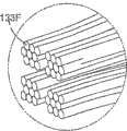
例如,图5A示出了六边形输出光纤图形133A,图5B示出了圆形输出光纤图形133B,图5C示出了环形输出光纤图形133C,图5D示出了三角形输出光纤图形133D,以及图5E示出了线形输出光纤图形133E。此外,如图5F所示,在选择性的示例性实施例中,可以提供分段的输出图形133F,其中对于特定的目标照明可以利用多个分开的光纤输出组。因为固定光纤输出端的条带可以由具有韧性的材料形成,如基于铅、锡和锌的材料和合金(或类似),在某些应用中,光纤输出图形可以被重配置。For example, Figure 5A shows a hexagonal
如图6A-6C所示,该固态发光器件的输出可以是易操纵的,以便可以同时或交替地照明一个或多个不同的方向。图6A示出了例如,在三个不同的组233A,233B和233C中布置的光纤输出端部233。例如,在正常条件下,固态发光器件可以通过端部233A可以在正向上提供输出照明。在车辆转向侧边的情况下,那么对应于输出光纤233B的LED管芯可以被激活(例如,通过触发例如转向信号指示器的信号,或通过将操纵轮转动设定量),以便可以通过输出光纤233B在该侧向提供附加照明。类似地,如果转向另一侧,对应于输出光纤233C的LED管芯可以被激活,以便在另一侧向中可以提供附加照明。As shown in Figures 6A-6C, the output of the solid state light emitting device can be steerable so that one or more different directions can be illuminated simultaneously or alternately. Figure 6A shows, for example, fiber output ends 233 arranged in three
另外,可以利用光纤的横向延伸输出布置提供易操纵的照明系统,如图5E所示,由此如下所述的失常(pixilation)控制电路(参见例如图9A和9B)可以从一侧至另一侧激活照明光纤块,例如,在转向或其他事件期间。以此方式,输出照明可以根据应用直接朝向(或远离)转向的方向。Additionally, a laterally extending output arrangement of optical fibers can be utilized to provide a maneuverable illumination system, as shown in FIG. 5E , whereby a pixilation control circuit (see, eg, FIGS. 9A and 9B ) as described below can be transferred from one side to the other. Side-activated lighting fiber optic blocks, for example, during turns or other events. In this way, the output lighting can be directed toward (or away from) the direction of the steering depending on the application.
以此方式,非机械方法可用于由该固态发光器件提供易操纵输出照明。另外,如本说明书中所给出的所属领域的普通技术人员将明白,可以利用更多或更少的光纤组。此外,该分组可以具有不同的相对取向,例如对于来自相同固态光源的高光束-低光束输出发射。In this way, non-mechanical methods can be used to provide easily steerable output lighting from the solid state light emitting device. Additionally, as will be apparent to one of ordinary skill in the art given this specification, more or fewer groups of fibers may be utilized. Furthermore, the groupings may have different relative orientations, eg for high beam-low beam output emissions from the same solid state light source.
在图6B中,示出了可以用来稳定和支撑不同光纤组的结构。例如,在光纤的输出端提供条带256。条带256可以提供第一孔径254、第二孔径254A和第三孔径254B,其中布置在孔径254A和254b中的光纤将输出方向不同于布置孔径254中的光纤的光。此外,如图6C所示,条带256可以被连接到外壳250或与外壳250集成,作为固态发光器件的支撑结构中的一部分。In Fig. 6B, a structure that can be used to stabilize and support different groups of optical fibers is shown. For example, a
另外,如图7所示,该固态发光器件可以由光纤输出端的一个光纤束产生易操纵的光。例如,光纤输出端133可以被设置在相同的位置,如图6B的输出孔径254。在该示例性实施例中,确定为光纤输出端129的这些输出端部的一部分以不同的角度被成角度抛光,以至基本上不同于光纤输出端133的剩余部分的角度(例如,相对于光纤轴10至50度)。所得的发射将处于不同于光纤端133的输出的方向。因此,与相对于图6A-6C的上述应用相类似,当用作汽车前灯时,该固态发光器件可以在正向(通过输出端133)和侧向(通过输出光纤129)中都提供输出照明。Alternatively, as shown in FIG. 7, the solid state light emitting device can generate steerable light from a fiber optic bundle at the output end of the fiber. For example, the
在提供易操纵照明的选择性实施例中,图13所示,从阵列连接器734延伸的光纤可以被包扎为多个偏离光纤束、中心光纤束730A和侧面光纤束730B和730C。由光纤束的输出端发射的光被多焦点透镜750接收,如非球面透镜,来自该偏离光纤束的输出变为希望的不同照明区751A,751B和751C。可以自动地和/或通过操作者控制来执行该易操纵照明。In an alternative embodiment to provide steerable illumination, as shown in FIG. 13, the fibers extending from the
在本发明的示例性实施例中,该固态发光器件可以用作照明源,例如在车辆前灯的应用中。例如,可以通过使用凸缘139来完成固定至现有前灯插座,图8所示。凸缘139可以被布置在光纤阵列连接器134的周边部分上。凸缘可以被设计成啮合在这种插座的锁定槽中。另外,凸缘可以形成在固态发光器件中的其他元件上,如外壳或聚光器基板上。In an exemplary embodiment of the invention, the solid state light emitting device may be used as a source of illumination, for example in vehicle headlight applications. For example, securing to an existing headlight socket can be accomplished through the use of
根据本发明的另一实施例,如图9A所示,提供一种照明系统300,允许可以用于孔径成形和/或动态光束移动的失常光控制。系统300包括固态光源301,其以类似于如上所述的固态光源100的方式构成。控制器304通过导线302和连接器310耦合到固态光源301,连接器310可以被连接到互连电路层。电源306被耦合到控制器304,以提供电源/电流到固态光源301。According to another embodiment of the present invention, as shown in Figure 9A, an illumination system 300 is provided that allows aberrant light control that can be used for aperture shaping and/or dynamic beam movement. System 300 includes a solid state light source 301 constructed in a manner similar to solid state
在示例性实施例中,控制器304被配置为有选择地激活包含于固态光源301中的各个LED管芯或LED管芯组。此外,因为光接收波导与LED管芯以一一对应设置,照明系统300可以提供失常输出。这类失常控制允许控制不同的颜色(例如,用于RGB输出的红、绿和蓝)或类似颜色的(例如,白色)LED管芯。In an exemplary embodiment, controller 304 is configured to selectively activate individual LED dies or groups of LED dies contained in solid state light source 301 . In addition, because the light-receiving waveguide is arranged in one-to-one correspondence with the LED die, the lighting system 300 can provide abnormal output. This type of aberration control allows control of LED dies of different colors (eg, red, green and blue for RGB output) or similar colors (eg, white).
图9B示出了可以对包含于固态发光器件中的LED管芯阵列提供失常的例子控制电路305。在该例子中,在LED管芯阵列中设置六十个LED管芯(LD1-LD60),这些管芯被集合成每二十个LED管芯的三个大组(314A-314C),每组进一步被分为较小的子分组或每五个LED管芯的沟道(例如,LD1-LD5)。总体,在该示例性实施例中,每个五个LED管芯的十二个沟道可以被分开地控制。在一个例子实施方案中,在RGB输出应用中,第一组LED管芯可以包括发红光的LED管芯,第二组LED管芯可以包括发蓝光的LED管芯以及第三组LED管芯可以包括发绿光的LED管芯。另外,在另一例子实施方案中,LED管芯的第一、第二和第三组可以包括发“白”光的LED管芯。FIG. 9B illustrates an
此外,该互连电路层也被设计成能为不同的LED管芯组提供分开的互连。根据在此描述的原理,也可以利用不同类型的LED管芯组,以及更大或更少数目的LED管芯。利用该结构,分开的RGB LED管芯沟道可以被驱动,以提供“白”或其他颜色输出。此外,由于LED管芯退化,特定的二极管沟道将失效或暗淡,在较高电流下,相邻沟道可能被驱动,以便输出照明看起来保持不变。因为互连层的(相对)宽LED管芯间隔和/或热管理能力,到某些LED管芯沟道的更大驱动电流将不会不利地影响总体性能。In addition, the interconnection circuit layer is also designed to provide separate interconnections for different groups of LED dies. Different types of groups of LED dies, as well as greater or lesser numbers of LED dies, may also be utilized in accordance with the principles described herein. Using this configuration, separate channels of RGB LED die can be driven to provide "white" or other color output. Also, as a particular diode channel will fail or dim due to LED die degradation, at higher currents the adjacent channel may be driven so that the output illumination appears to remain constant. Because of the (relatively) wide LED die spacing and/or thermal management capabilities of the interconnect layers, higher drive currents to certain LED die channels will not adversely affect overall performance.
此外,可以在互连电路层(或其它事宜的位置)上设置温度传感器(未示出),来感应在或者靠近不同LED管芯沟道的温度变化。这样,控制电路305可用来变化特定沟道中的电流总量,以补偿由于提高的温度而在该沟道中的光输出中的通常减小。In addition, temperature sensors (not shown) can be placed on the interconnect circuit layer (or other matter locations) to sense temperature changes in or near the channels of the different LED dies. In this way, the
更详细地,通过电源306电路305接收电压。该电压通过升压转换器芯片312A-312C和它们的相关电子设备(未示出)变为调整的输出电流/电压源。以此方式,来自电源306的电压变化可以被减轻,提供给LED管芯的电流/电压保持在调整级别。芯片312A-312C可以包括,例如,可以从National Semiconductor获得的LM2733芯片。在该示例性实施例中,在80-100mA下,驱动电压/电流参数可以约为20伏,因此为整个LED管芯阵列提供总共约1.0至1.2A。然后驱动电流/电压被提供给阵列内的不同LED管芯沟道。在该例子中,每个LED管芯正常地将需要约20mA偏置电流,偏压阈值随电流增加而增加,对于典型的GaN基LED管芯接近约4.0V。当然,不同的LED管芯效率或成分可能需要不同的偏压和驱动电平。In more detail, the
此外,在电路305中可以包括电阻器/电热调节器链316,以设置每个LED管芯沟道的总最大电流。此外,可以提供开关组318,包括相应数目的LED管芯沟道电子开关,由此每个LED管芯沟道被耦合/去耦合到地线(或电源,根据相对于LED管芯沟道的开关组排列),以便激活每个特定的LED管芯沟道。开关组318可以被微控制器(未示出)或遥控开关(例如,转向信号)自动地控制,基于特定应用需要的照明参数。当然,该电路结构允许许多实施方案和取代,如本说明书给出的技术领域的普通技术人员所理解。例如,控制电路305可以被实现为利用相同的电流驱动所有LED管芯,或者给定的LED管芯沟道可以被自动地或依命令导通/截止。通过增加固定或可变电阻到开关组的开关脚,不同电流可以被施加到每个沟道。Additionally, a resistor/
图10示出了可以用于“冷”前灯应用中所利用的示例性固态发光器件401的示意图。例如,固态发光器件401被布置在汽车或其它车辆(未示出)的前灯隔离室402中,该固态发光器件401可以根据如上所述的实施例配置。通过可滑动啮合的凸缘439的使用,发光器件401可以被固定在隔室402中,该可滑动啮合的凸缘439被配置为在插座的狭槽438内滑动和锁定。因此,从光输出方向散发热量的热沉440位于分开的隔室404,例如汽车或其它车辆的内部发动机隔离室中。通过光学元件415光束成形的输出照明可以被集中/聚焦为基于需要的照明图形。光学元件415可以被设计成提供符合当前安全组织(例如,NHTSA)标准的选择的输出图形。例子光学元件可以包括非球面/变形的光学元件,和/或间断和/或非分析的(键槽(spline))光学元件。FIG. 10 shows a schematic diagram of an exemplary solid state light emitting
利用该方法,可以避免使用在前灯隔室402中布置的复杂反射光学元件,此外,因为热量从隔室402散逸,因此不必特别热处理隔室402中的任意剩余的光学元件,因此避免由暴露于频繁的高强度热量可能引起的性能下降。此外,如果固态发光器件401设有输出光纤和输出孔径结构,如图6A-6C所示,可以完成易操纵的输出照明,不必利用当前由常规HID灯操纵输出时必须采用的移动镜子,灯泡和/或镜头机构。Using this approach, the use of complex reflective optics arranged in the
在此描述的固态发光器件也可以用于其他应用。例如,图11示出了示意性牙科固化应用,在牙科固化设备500中包含固态发光器件501(具有与图1A和1B和/或其他实施例类似的结构)。该固态发光器件501可以被布置在牙科固化设备500的处理部分510中。此外,用来容纳和引导来自LED管芯或其他固态光产生源输出的输出光纤可以贯穿光传递臂525,该光传递臂525可以被直接放置在可固化材料上。在该应用中,可以根据接收该照明的材料的固化外表利用UV和/或蓝光辐射源。The solid state light emitting devices described herein can also be used in other applications. For example, Figure 11 shows an exemplary dental curing application incorporating a solid state light emitting device 501 (with a structure similar to Figures IA and IB and/or other embodiments) in a
在还一替换实施例中,图12示出示意性大批材料固化设备,如织物(web)固化台。例如,在粘合、带或基于织物的制造中,粘合剂常常是蓝光/UV可固化材料,其必须在不同的材料或基底上固化。在常规方法中,高强度放电和弧光灯常常用来执行固化工序。但是,这些常规灯辐射360度的光和热量,因此需要复杂的热交换和/或冷却机构。另外,在某些常规方法中,基底材料和UV固化剂必须适合于承受高强度热量。In yet another alternative embodiment, Figure 12 shows a schematic bulk material curing apparatus, such as a web curing station. For example, in adhesive, tape, or fabric-based manufacturing, the adhesive is often a blue/UV curable material that must be cured on a different material or substrate. In conventional methods, high intensity discharge and arc lamps are often used to perform the curing process. However, these conventional lamps radiate 360 degrees of light and heat, thus requiring complex heat exchange and/or cooling mechanisms. Additionally, in some conventional methods, the substrate material and UV curing agent must be suitable for withstanding high levels of heat.
图12提供在常规固化系统中发现的发热问题的一种解决办法,其中固化台600包括固态发光器件604(类似于如上所述的实施例构成),固态发光器件的热散逸或热沉元件可以位于热交换单元602中。如上所述,通过适当的LED空间、导热互连电路和/或热沉,由固态发光器件的辐射源产生的热量从光输出的方向散逸。Figure 12 provides a solution to the heat generation problem found in conventional curing systems, wherein a curing
此外,固态发光器件604可以发出高度集中的辐射到可辐射固化的材料,因此减小由固化的不足深度引起的有害效应。LED管芯或其他辐射产生源的集中输出可以被波导阵列聚集和引导,该波导阵列布置在张力减轻外壳630中,并传递给设置在基底652上的辐射可固化材料或配方650。基底652可以被布置在移动平台或输送带上,以提供用于大量材料的连续固化。如上面相对于图5A-5F所述,波导的输出端,例如光纤,可以被布置在大量不同的可重配置图形中,因此制成固态发光器件,特别适合于固化具有各种各样形状的材料和/或固化深度需要。In addition, the solid state light emitting
在还一应用中,在此描述的固态光源可用在投射系统中。由于提供失常输出的能力,LED管芯阵列可包括用于RGB输出的不同输出颜色LED管芯。此外,为了渐进的扫描,可以多路复用输出,以提供适宜的投射图像。此外,上述实施例的固态光源可用作LCD显示器的背光的源。具体地,当对于“白”发射使用磷涂敷的管芯时,失常的白色LED管芯可提供LCD显示器的增加的对比度。In yet another application, the solid state light sources described herein may be used in projection systems. Due to the ability to provide aliased outputs, the array of LED dies may include different output color LED dies for RGB output. Additionally, the outputs can be multiplexed for progressive scanning to provide a suitable projected image. Furthermore, the solid-state light source of the above-described embodiments can be used as a source for a backlight of an LCD display. In particular, aberrant white LED dies can provide increased contrast for LCD displays when phosphor-coated dies are used for "white" emission.
尽管参考示例性优选实施例叙述了本发明,但是在不脱离本发明的范围的条件下,本发明可以以其他特定的形式体现。由此,应理解在此叙述和图示的实施例仅仅是示例性的,不应该被认为是限制本发明的范围。根据本发明的范围可以进行其他改变和改进。Although the invention has been described with reference to exemplary preferred embodiments, the invention may be embodied in other specific forms without departing from the scope of the invention. Accordingly, it should be understood that the embodiments described and illustrated herein are exemplary only, and should not be taken as limiting the scope of the invention. Other changes and modifications can be made within the scope of the present invention.
Claims (13)
Applications Claiming Priority (2)
| Application Number | Priority Date | Filing Date | Title |
|---|---|---|---|
| US10/726,225US7329887B2 (en) | 2003-12-02 | 2003-12-02 | Solid state light device |
| US10/726,225 | 2003-12-02 |
Publications (2)
| Publication Number | Publication Date |
|---|---|
| CN1914527A CN1914527A (en) | 2007-02-14 |
| CN100565253Ctrue CN100565253C (en) | 2009-12-02 |
Family
ID=34700342
Family Applications (1)
| Application Number | Title | Priority Date | Filing Date |
|---|---|---|---|
| CNB200480041274XAExpired - Fee RelatedCN100565253C (en) | 2003-12-02 | 2004-10-27 | Sony ericsson mobile comm ab |
Country Status (7)
| Country | Link |
|---|---|
| US (1) | US7329887B2 (en) |
| EP (1) | EP1700144A1 (en) |
| JP (1) | JP2007513378A (en) |
| KR (1) | KR20060110341A (en) |
| CN (1) | CN100565253C (en) |
| TW (1) | TW200527718A (en) |
| WO (1) | WO2005062089A1 (en) |
Cited By (3)
| Publication number | Priority date | Publication date | Assignee | Title |
|---|---|---|---|---|
| CN104105921A (en)* | 2012-12-20 | 2014-10-15 | 齐扎拉光系统有限责任公司 | Light-emitting unit for projector lamp |
| CN108139061A (en)* | 2015-10-23 | 2018-06-08 | Zkw集团有限责任公司 | For the micro projection optical module for light distribution of the generation without image error of motor-driven vehicle headlight adapter |
| CN110476008A (en)* | 2017-04-06 | 2019-11-19 | 株式会社小糸制作所 | Three-dimensional flat-panel display device and display apparatus |
Families Citing this family (116)
| Publication number | Priority date | Publication date | Assignee | Title |
|---|---|---|---|---|
| US9167959B1 (en)* | 2010-03-26 | 2015-10-27 | Optech Ventures, Llc | Illumination for enhanced contrast in debridement apparatus and method |
| US6200134B1 (en) | 1998-01-20 | 2001-03-13 | Kerr Corporation | Apparatus and method for curing materials with radiation |
| US7182597B2 (en) | 2002-08-08 | 2007-02-27 | Kerr Corporation | Curing light instrument |
| AU2003297588A1 (en)* | 2002-12-02 | 2004-06-23 | 3M Innovative Properties Company | Illumination system using a plurality of light sources |
| JP2006516828A (en)* | 2003-01-27 | 2006-07-06 | スリーエム イノベイティブ プロパティズ カンパニー | Phosphorescent light source element and manufacturing method |
| US7456805B2 (en)* | 2003-12-18 | 2008-11-25 | 3M Innovative Properties Company | Display including a solid state light device and method using same |
| US20070261792A1 (en)* | 2004-02-23 | 2007-11-15 | Anderson Gordon L | Locator Tool Assembly for Paint Replacement Films |
| WO2006007388A1 (en)* | 2004-06-16 | 2006-01-19 | 3M Innovative Properties Company | Solid state light device |
| US7213958B2 (en)* | 2004-06-30 | 2007-05-08 | 3M Innovative Properties Company | Phosphor based illumination system having light guide and an interference reflector |
| US7255469B2 (en)* | 2004-06-30 | 2007-08-14 | 3M Innovative Properties Company | Phosphor based illumination system having a light guide and an interference reflector |
| US7204631B2 (en)* | 2004-06-30 | 2007-04-17 | 3M Innovative Properties Company | Phosphor based illumination system having a plurality of light guides and an interference reflector |
| US7182498B2 (en)* | 2004-06-30 | 2007-02-27 | 3M Innovative Properties Company | Phosphor based illumination system having a plurality of light guides and an interference reflector |
| US7204630B2 (en)* | 2004-06-30 | 2007-04-17 | 3M Innovative Properties Company | Phosphor based illumination system having a plurality of light guides and an interference reflector |
| US7390097B2 (en)* | 2004-08-23 | 2008-06-24 | 3M Innovative Properties Company | Multiple channel illumination system |
| DE102004056252A1 (en) | 2004-10-29 | 2006-05-04 | Osram Opto Semiconductors Gmbh | Lighting device, vehicle headlight and method for producing a lighting device |
| US8459852B2 (en) | 2007-10-05 | 2013-06-11 | Dental Equipment, Llc | LED-based dental exam lamp |
| US8113830B2 (en) | 2005-05-27 | 2012-02-14 | Kerr Corporation | Curing light instrument |
| US7479660B2 (en) | 2005-10-21 | 2009-01-20 | Perkinelmer Elcos Gmbh | Multichip on-board LED illumination device |
| KR100735254B1 (en)* | 2005-12-09 | 2007-07-03 | 삼성전자주식회사 | Optical fiber array module, manufacturing method and portable terminal |
| DE102005061204A1 (en)* | 2005-12-21 | 2007-07-05 | Perkinelmer Elcos Gmbh | Lighting device, lighting control device and lighting system |
| US20070171638A1 (en)* | 2006-01-24 | 2007-07-26 | Sbc Knowledge Ventures, L.P. | Apparatus and methods for transmitting light over optical fibers |
| US7413327B2 (en) | 2006-04-10 | 2008-08-19 | The Boeing Company | Vehicle lighting fixture |
| US7625103B2 (en)* | 2006-04-21 | 2009-12-01 | Cree, Inc. | Multiple thermal path packaging for solid state light emitting apparatus and associated assembling methods |
| US7648257B2 (en) | 2006-04-21 | 2010-01-19 | Cree, Inc. | Light emitting diode packages |
| JP5243439B2 (en)* | 2006-10-06 | 2013-07-24 | スリーエム イノベイティブ プロパティズ カンパニー | Backlight module for autostereoscopic 3D display device and scanning backlight for LCD device |
| US8498695B2 (en) | 2006-12-22 | 2013-07-30 | Novadaq Technologies Inc. | Imaging system with a single color image sensor for simultaneous fluorescence and color video endoscopy |
| US8258682B2 (en)* | 2007-02-12 | 2012-09-04 | Cree, Inc. | High thermal conductivity packaging for solid state light emitting apparatus and associated assembling methods |
| US7677777B2 (en) | 2007-02-21 | 2010-03-16 | Magna International, Inc. | LED apparatus for world homologation |
| TWI378580B (en)* | 2007-03-07 | 2012-12-01 | Everlight Electronics Co Ltd | Socket led device |
| CN101790660B (en)* | 2007-05-07 | 2013-10-09 | 科锐公司 | Lamps and lighting fixtures |
| DE102007028075B4 (en)* | 2007-06-15 | 2009-03-12 | Zett Optics Gmbh | LED light source and method for driving and stabilizing an LED light source |
| KR101425796B1 (en)* | 2007-10-08 | 2014-08-04 | 삼성전자주식회사 | Multi-metal waveguide and Manufacturing method thereof |
| FR2922306B1 (en)* | 2007-10-12 | 2009-11-20 | Sp3H | SPECTROMETRY DEVICE FOR ANALYSIS OF A FLUID |
| FR2922304B1 (en)* | 2007-10-12 | 2009-11-20 | Sp3H | SPECTROMETRY DEVICE FOR ANALYSIS OF A FLUID |
| FR2922303B1 (en)* | 2007-10-12 | 2010-05-07 | Sp3H | SPECTROMETRY DEVICE FOR ANALYSIS OF A FLUID |
| KR100963966B1 (en)* | 2007-11-21 | 2010-06-15 | 현대모비스 주식회사 | LED unit and light source module having same |
| DE102007063262A1 (en)* | 2007-12-17 | 2009-06-18 | Storz Endoskop Produktions Gmbh | Illumination device for generating light and for coupling the light into a proximal end of a light guide cable of an observation device for endoscopy or microscopy |
| JP5117878B2 (en)* | 2008-02-13 | 2013-01-16 | 富士フイルム株式会社 | Endoscope light source device |
| KR101517264B1 (en) | 2008-03-18 | 2015-05-04 | 노바다크 테크놀러지즈 인코포레이티드 | Imaging system for combined full-color reflectance and near-infrared imaging |
| KR20100128336A (en)* | 2008-03-21 | 2010-12-07 | 나노그램 코포레이션 | Metal silicon nitride or metal silicon oxynitride submicron phosphor particles and methods of synthesizing these phosphors |
| DE102008022414B4 (en)* | 2008-05-06 | 2013-03-14 | Rüdiger Lanz | Illuminants for use in street lighting and a device for street lighting |
| US8378661B1 (en)* | 2008-05-29 | 2013-02-19 | Alpha-Omega Power Technologies, Ltd.Co. | Solar simulator |
| JP2010072494A (en)* | 2008-09-19 | 2010-04-02 | Sanyo Electric Co Ltd | Illuminating device and projection video display apparatus |
| US8189189B1 (en) | 2008-10-08 | 2012-05-29 | Herendeen Robert O | LED sensor for process control |
| US8384682B2 (en)* | 2009-01-08 | 2013-02-26 | Industrial Technology Research Institute | Optical interactive panel and display system with optical interactive panel |
| US8247886B1 (en) | 2009-03-09 | 2012-08-21 | Soraa, Inc. | Polarization direction of optical devices using selected spatial configurations |
| US9072572B2 (en) | 2009-04-02 | 2015-07-07 | Kerr Corporation | Dental light device |
| US9066777B2 (en) | 2009-04-02 | 2015-06-30 | Kerr Corporation | Curing light device |
| JP2012528469A (en)* | 2009-05-29 | 2012-11-12 | ザ リージェンツ オブ ザ ユニバーシティ オブ ミシガン | Solid state light source based on hybrid waveguide, down converter and diffuser |
| US9583678B2 (en) | 2009-09-18 | 2017-02-28 | Soraa, Inc. | High-performance LED fabrication |
| KR101107561B1 (en)* | 2009-11-12 | 2012-01-31 | (주)화이버 옵틱코리아 | Fiber optic integrated LED lighting device |
| EP2512322A4 (en)* | 2009-12-17 | 2013-09-18 | Alcon Res Ltd | Photonic lattice leds for ophthalmic illumination |
| US20110148304A1 (en)* | 2009-12-22 | 2011-06-23 | Artsyukhovich Alexander N | Thermoelectric cooling for increased brightness in a white light l.e.d. illuminator |
| WO2011078958A1 (en)* | 2009-12-23 | 2011-06-30 | Alcon Research, Ltd. | Enhanced led illuminator |
| US8258524B2 (en) | 2010-01-26 | 2012-09-04 | Sharp Kabushiki Kaisha | Light emitting diode device |
| US20110186874A1 (en)* | 2010-02-03 | 2011-08-04 | Soraa, Inc. | White Light Apparatus and Method |
| US10147850B1 (en) | 2010-02-03 | 2018-12-04 | Soraa, Inc. | System and method for providing color light sources in proximity to predetermined wavelength conversion structures |
| WO2011111170A1 (en)* | 2010-03-09 | 2011-09-15 | Necディスプレイソリューションズ株式会社 | Illumination device, and projection display device using same |
| US9314374B2 (en)* | 2010-03-19 | 2016-04-19 | Alcon Research, Ltd. | Stroboscopic ophthalmic illuminator |
| DE102010036496A1 (en)* | 2010-04-23 | 2011-10-27 | Degudent Gmbh | Method and device for coupling radiation emitted by LEDs |
| US9450143B2 (en) | 2010-06-18 | 2016-09-20 | Soraa, Inc. | Gallium and nitrogen containing triangular or diamond-shaped configuration for optical devices |
| TWI520386B (en)* | 2010-07-29 | 2016-02-01 | 神基科技股份有限公司 | Structure of light emitting diode assembly and manufacturing method thereof |
| US8297790B2 (en)* | 2010-08-18 | 2012-10-30 | Lg Innotek Co., Ltd. | Lamp device |
| US8573801B2 (en) | 2010-08-30 | 2013-11-05 | Alcon Research, Ltd. | LED illuminator |
| KR101742678B1 (en)* | 2010-09-17 | 2017-06-01 | 엘지이노텍 주식회사 | Lamp apparatus |
| TWI440794B (en) | 2010-09-27 | 2014-06-11 | Ind Tech Res Inst | Solar light simulator |
| US10267506B2 (en)* | 2010-11-22 | 2019-04-23 | Cree, Inc. | Solid state lighting apparatuses with non-uniformly spaced emitters for improved heat distribution, system having the same, and methods having the same |
| CN103765091B (en) | 2011-03-08 | 2017-09-26 | 诺瓦达克技术公司 | Full Spectrum LED Illuminators |
| WO2012173507A1 (en)* | 2011-06-14 | 2012-12-20 | Freescale Semiconductor, Inc. | Circuit arrangement, lighting apparatus and method of crosstalk-compensated current sensing |
| US8686431B2 (en) | 2011-08-22 | 2014-04-01 | Soraa, Inc. | Gallium and nitrogen containing trilateral configuration for optical devices |
| WO2013112435A1 (en) | 2012-01-24 | 2013-08-01 | Cooledge Lighting Inc. | Light - emitting devices having discrete phosphor chips and fabrication methods |
| US8896010B2 (en) | 2012-01-24 | 2014-11-25 | Cooledge Lighting Inc. | Wafer-level flip chip device packages and related methods |
| US8907362B2 (en) | 2012-01-24 | 2014-12-09 | Cooledge Lighting Inc. | Light-emitting dies incorporating wavelength-conversion materials and related methods |
| DE102012206971A1 (en)* | 2012-04-26 | 2013-10-31 | Osram Gmbh | OPTICAL DEVICE AND LIGHTING DEVICE |
| AT512865B1 (en)* | 2012-05-09 | 2014-12-15 | Zizala Lichtsysteme Gmbh | Lighting device for a motor vehicle headlight and light module and motor vehicle headlight with lighting device |
| WO2013181594A1 (en)* | 2012-06-01 | 2013-12-05 | Revolution Display | Light-emitting assembly and light-emitting floor system |
| JP2014010918A (en)* | 2012-06-27 | 2014-01-20 | Sharp Corp | Luminaire and vehicle headlight |
| US9978904B2 (en) | 2012-10-16 | 2018-05-22 | Soraa, Inc. | Indium gallium nitride light emitting devices |
| FR2999333A1 (en)* | 2012-12-07 | 2014-06-13 | Sp3H | Method for controlling spectrometer to analyze e.g. hydrocarbons used as fuel of heat engine in e.g. terrestrial vehicle, involves adjusting integration duration of photosensitive cells to determined value of integration duration |
| CN104969058B (en)* | 2012-12-07 | 2017-08-08 | Sp3H公司 | On-board apparatus and method for analysing a fluid in a heat engine |
| TWI473141B (en)* | 2012-12-13 | 2015-02-11 | Eternal Materials Co Ltd | A radiation curing apparatus |
| AT513816B1 (en)* | 2012-12-20 | 2015-11-15 | Zizala Lichtsysteme Gmbh | Light guide unit for a lighting unit of a headlamp and lighting unit and headlamp |
| US9761763B2 (en) | 2012-12-21 | 2017-09-12 | Soraa, Inc. | Dense-luminescent-materials-coated violet LEDs |
| AT513917B1 (en)* | 2013-02-05 | 2014-11-15 | Zizala Lichtsysteme Gmbh | Lighting unit for a headlight and headlights |
| US9419189B1 (en) | 2013-11-04 | 2016-08-16 | Soraa, Inc. | Small LED source with high brightness and high efficiency |
| DE102013113511A1 (en) | 2013-12-05 | 2015-06-11 | Karl Storz Gmbh & Co. Kg | Endoscope, exoscope or microscope and method for illuminating an operating area of an endoscope, exoscope or microscope |
| US9343443B2 (en) | 2014-02-05 | 2016-05-17 | Cooledge Lighting, Inc. | Light-emitting dies incorporating wavelength-conversion materials and related methods |
| KR20160007766A (en)* | 2014-06-27 | 2016-01-21 | 삼성전자주식회사 | Light emitting module |
| AU2015346153B2 (en)* | 2014-11-14 | 2019-12-12 | Boston Scientific Scimed, Inc. | Surgical laser systems and laser devices |
| EP4335494A3 (en) | 2015-02-27 | 2024-05-15 | Colgate-Palmolive Company | Oral treatment system |
| EP3275021B1 (en) | 2015-03-26 | 2020-05-06 | Lumileds Holding B.V. | Light source |
| AU2016351730B2 (en) | 2015-11-13 | 2019-07-11 | Novadaq Technologies Inc. | Systems and methods for illumination and imaging of a target |
| WO2017127929A1 (en) | 2016-01-26 | 2017-08-03 | Novadaq Technologies Inc. | Configurable platform |
| USD916294S1 (en) | 2016-04-28 | 2021-04-13 | Stryker European Operations Limited | Illumination and imaging device |
| EP3469420A4 (en) | 2016-06-14 | 2020-02-12 | Novadaq Technologies ULC | METHODS AND SYSTEMS FOR ADAPTIVE IMAGING FOR THE AMPLIFICATION OF A WEAK LIGHT SIGNAL IN A MEDICAL VISUALIZATION |
| US11172560B2 (en) | 2016-08-25 | 2021-11-09 | Alcon Inc. | Ophthalmic illumination system with controlled chromaticity |
| DE102016122861A1 (en)* | 2016-11-28 | 2018-05-30 | HELLA GmbH & Co. KGaA | Lighting device for vehicles |
| EP3580609B1 (en) | 2017-02-10 | 2023-05-24 | Stryker European Operations Limited | Open-field handheld fluorescence imaging systems and methods |
| JP6865396B2 (en)* | 2017-02-27 | 2021-04-28 | パナソニックIpマネジメント株式会社 | Lighting equipment, lighting systems, and moving objects |
| US10222022B2 (en)* | 2017-07-06 | 2019-03-05 | Valeo North America, Inc. | Covered fiber bundle for lighting modules |
| DE102017115739A1 (en) | 2017-07-13 | 2019-01-17 | Karl Storz Se & Co. Kg | Imaging medical instrument such as an endoscope, an exoscope or a microscope |
| US10596952B2 (en)* | 2017-09-13 | 2020-03-24 | Shanghai Koito Automotive Lamp Co., Ltd. | Intelligent lighting system for automobile lamp, automobile lamp assembly and automobile |
| EP3604902A1 (en) | 2018-08-03 | 2020-02-05 | ZKW Group GmbH | Optical device for a motor vehicle headlight comprising light guides |
| EP3608585A1 (en)* | 2018-08-07 | 2020-02-12 | ZKW Group GmbH | Projection device from a plurality of micro-optics systems and a light module for a motor vehicle headlamp |
| CN110887013B (en)* | 2018-09-07 | 2021-12-31 | Sl株式会社 | Vehicle lamp |
| KR102570603B1 (en)* | 2019-01-28 | 2023-08-24 | 아크소프트 코포레이션 리미티드 | Proximity ambient light sensor package |
| CN109917609B (en)* | 2019-03-21 | 2024-06-11 | 成都九天画芯科技有限公司 | Liquid crystal projector capable of effectively reducing screen temperature |
| US20200338220A1 (en)* | 2019-04-27 | 2020-10-29 | Gerald Ho Kim | UV-C Illumination System For Disinfection |
| WO2021016119A1 (en)* | 2019-07-19 | 2021-01-28 | Schott Corporation | Emitter array and light combiner assembly |
| CN110906282A (en)* | 2020-01-02 | 2020-03-24 | 北京理工大学重庆创新中心 | Lamp with variable color temperature and color based on optical light collector |
| US11163100B2 (en) | 2020-01-28 | 2021-11-02 | Lucifer Lighting Company | Light fixtures having waveguides and related methods |
| USD995885S1 (en) | 2020-01-28 | 2023-08-15 | Lucifer Lighting Company | Waveguide for multi-zone illumination light fixtures |
| DE102020123031A1 (en) | 2020-09-03 | 2022-03-03 | Karl Storz Se & Co. Kg | Lighting device with optical fiber detection |
| CN112130251A (en)* | 2020-09-21 | 2020-12-25 | 中国科学院长春光学精密机械与物理研究所 | Optical fiber positioner and positioning method thereof |
| CN115095837B (en)* | 2022-05-06 | 2024-03-15 | 中国第一汽车股份有限公司 | Variable luminous car lamp system realized based on optical fiber and control method thereof |
| US20230369528A1 (en)* | 2022-05-14 | 2023-11-16 | Xintec Inc. | Chip package and manufacturing method thereof |
Family Cites Families (145)
| Publication number | Priority date | Publication date | Assignee | Title |
|---|---|---|---|---|
| US489771A (en)* | 1893-01-10 | Sole-leveling machine | ||
| US3825335A (en) | 1973-01-04 | 1974-07-23 | Polaroid Corp | Variable color photographic lighting system |
| US3902059A (en) | 1974-02-15 | 1975-08-26 | Esquire Inc | Light reflector system |
| US4254453A (en) | 1978-08-25 | 1981-03-03 | General Instrument Corporation | Alpha-numeric display array and method of manufacture |
| EP0031211B1 (en) | 1979-12-22 | 1984-10-03 | LUCAS INDUSTRIES public limited company | Motor vehicle lamp reflector |
| JPS6019564A (en) | 1983-07-13 | 1985-01-31 | Fuji Photo Film Co Ltd | Side printer |
| US5693043A (en) | 1985-03-22 | 1997-12-02 | Massachusetts Institute Of Technology | Catheter for laser angiosurgery |
| EP0249934A3 (en) | 1986-06-18 | 1990-06-06 | Mitsubishi Rayon Co., Ltd. | Optical fiber device |
| US4755918A (en) | 1987-04-06 | 1988-07-05 | Lumitex, Inc. | Reflector system |
| US4914731A (en) | 1987-08-12 | 1990-04-03 | Chen Shen Yuan | Quickly formed light emitting diode display and a method for forming the same |
| US4897771A (en) | 1987-11-24 | 1990-01-30 | Lumitex, Inc. | Reflector and light system |
| US5146248A (en) | 1987-12-23 | 1992-09-08 | North American Philips Corporation | Light valve projection system with improved illumination |
| FR2630550A1 (en) | 1988-04-22 | 1989-10-27 | Radiotechnique Compelec | METHOD FOR MOUNTING OPTICAL ELEMENTS ON A SUPPORT AND OPTICAL CIRCUIT THUS OBTAINED |
| JPH02142695A (en) | 1988-07-13 | 1990-05-31 | Sony Corp | Laser beam machine |
| US4964025A (en) | 1988-10-05 | 1990-10-16 | Hewlett-Packard Company | Nonimaging light source |
| JPH081964B2 (en) | 1989-01-18 | 1996-01-10 | 株式会社小糸製作所 | Flexible display device |
| US5155336A (en) | 1990-01-19 | 1992-10-13 | Applied Materials, Inc. | Rapid thermal heating apparatus and method |
| JPH088463Y2 (en) | 1990-03-15 | 1996-03-06 | 日本信号株式会社 | AC detection circuit diagnostic device |
| JPH0437596A (en) | 1990-06-01 | 1992-02-07 | Toshiba Corp | Wiring board equipment |
| US5212710A (en) | 1990-07-19 | 1993-05-18 | Sony Corporation | Laser light beam synthesizing apparatus |
| DE69129182T2 (en) | 1990-12-07 | 1998-09-03 | Stanley Electric Co Ltd | Light irradiation device with light emitting diode as light source |
| US5227008A (en) | 1992-01-23 | 1993-07-13 | Minnesota Mining And Manufacturing Company | Method for making flexible circuits |
| DE4301716C2 (en) | 1992-02-04 | 1999-08-12 | Hitachi Ltd | Projection exposure device and method |
| US5299222A (en) | 1992-03-11 | 1994-03-29 | Lightwave Electronics | Multiple diode laser stack for pumping a solid-state laser |
| US5301090A (en)* | 1992-03-16 | 1994-04-05 | Aharon Z. Hed | Luminaire |
| US5293437A (en) | 1992-06-03 | 1994-03-08 | Visual Optics, Inc. | Fiber optic display with direct driven optical fibers |
| US5265792A (en) | 1992-08-20 | 1993-11-30 | Hewlett-Packard Company | Light source and technique for mounting light emitting diodes |
| US5317484A (en) | 1993-02-01 | 1994-05-31 | General Electric Company | Collection optics for high brightness discharge light source |
| US5810469A (en) | 1993-03-26 | 1998-09-22 | Weinreich; Steve | Combination light concentrating and collimating device and light fixture and display screen employing the same |
| US5534718A (en) | 1993-04-12 | 1996-07-09 | Hsi-Huang Lin | LED package structure of LED display |
| US5420768A (en) | 1993-09-13 | 1995-05-30 | Kennedy; John | Portable led photocuring device |
| DE4341234C2 (en) | 1993-12-03 | 2002-09-12 | Bosch Gmbh Robert | Lighting device for vehicles |
| US5882774A (en) | 1993-12-21 | 1999-03-16 | Minnesota Mining And Manufacturing Company | Optical film |
| EP0742940A4 (en) | 1994-01-31 | 1998-09-30 | Sdl Inc | Laser illuminated display system |
| JP2979522B2 (en) | 1994-02-28 | 1999-11-15 | 株式会社島津製作所 | Light source device for curing photo-curable resin |
| US5580471A (en) | 1994-03-30 | 1996-12-03 | Panasonic Technologies, Inc. | Apparatus and method for material treatment and inspection using fiber-coupled laser diode |
| DE4429913C1 (en) | 1994-08-23 | 1996-03-21 | Fraunhofer Ges Forschung | Device and method for plating |
| DE4430778C2 (en) | 1994-08-30 | 2000-01-27 | Sick Ag | Tube |
| US6152588A (en) | 1994-09-28 | 2000-11-28 | Sdl, Inc. | Addressable vehicular lighting system |
| US5713654A (en) | 1994-09-28 | 1998-02-03 | Sdl, Inc. | Addressable laser vehicle lights |
| US5611017A (en) | 1995-06-01 | 1997-03-11 | Minnesota Mining And Manufacturing Co. | Fiber optic ribbon cable with pre-installed locations for subsequent connectorization |
| US5574817A (en) | 1995-06-01 | 1996-11-12 | Minnesota Mining And Manufacturing Company | Fiber optic ribbon cable assembly and method of manufacturing same |
| US5629996A (en) | 1995-11-29 | 1997-05-13 | Physical Optics Corporation | Universal remote lighting system with nonimaging total internal reflection beam transformer |
| US6239868B1 (en) | 1996-01-02 | 2001-05-29 | Lj Laboratories, L.L.C. | Apparatus and method for measuring optical characteristics of an object |
| US5661839A (en) | 1996-03-22 | 1997-08-26 | The University Of British Columbia | Light guide employing multilayer optical film |
| US6045240A (en) | 1996-06-27 | 2000-04-04 | Relume Corporation | LED lamp assembly with means to conduct heat away from the LEDS |
| US5816694A (en) | 1996-06-28 | 1998-10-06 | General Electric Company | Square distribution reflector |
| DE19626176A1 (en) | 1996-06-29 | 1998-01-08 | Deutsche Forsch Luft Raumfahrt | Lithography exposure device and lithography method |
| FI103074B1 (en) | 1996-07-17 | 1999-04-15 | Valtion Teknillinen | spectrometer |
| US6608332B2 (en) | 1996-07-29 | 2003-08-19 | Nichia Kagaku Kogyo Kabushiki Kaisha | Light emitting device and display |
| US5808794A (en) | 1996-07-31 | 1998-09-15 | Weber; Michael F. | Reflective polarizers having extended red band edge for controlled off axis color |
| US5709463A (en) | 1996-08-13 | 1998-01-20 | Delco Electronics Corporation | Backlighting for bright liquid crystal display |
| US5727108A (en) | 1996-09-30 | 1998-03-10 | Troy Investments, Inc. | High efficiency compound parabolic concentrators and optical fiber powered spot luminaire |
| US6104446A (en) | 1996-12-18 | 2000-08-15 | Blankenbecler; Richard | Color separation optical plate for use with LCD panels |
| JP3894613B2 (en) | 1997-03-14 | 2007-03-22 | 株式会社フジクラ | Flexible printed wiring board |
| US6587573B1 (en)* | 2000-03-20 | 2003-07-01 | Gentex Corporation | System for controlling exterior vehicle lights |
| JPH10319871A (en) | 1997-05-19 | 1998-12-04 | Kouha:Kk | LED display device |
| CN1217130C (en) | 1997-06-30 | 2005-08-31 | 株式会社丰臣 | Face-plate for operating machine |
| US6952504B2 (en) | 2001-12-21 | 2005-10-04 | Neophotonics Corporation | Three dimensional engineering of planar optical structures |
| US5967653A (en) | 1997-08-06 | 1999-10-19 | Miller; Jack V. | Light projector with parabolic transition format coupler |
| US6340824B1 (en) | 1997-09-01 | 2002-01-22 | Kabushiki Kaisha Toshiba | Semiconductor light emitting device including a fluorescent material |
| US5909037A (en) | 1998-01-12 | 1999-06-01 | Hewlett-Packard Company | Bi-level injection molded leadframe |
| US6200134B1 (en) | 1998-01-20 | 2001-03-13 | Kerr Corporation | Apparatus and method for curing materials with radiation |
| CH689339A5 (en) | 1998-02-12 | 1999-02-26 | Staufert Gerhard | LED illumination panel |
| JPH11284233A (en) | 1998-03-27 | 1999-10-15 | Stanley Electric Co Ltd | Surface mount type LED element |
| US6290382B1 (en) | 1998-08-17 | 2001-09-18 | Ppt Vision, Inc. | Fiber bundle combiner and led illumination system and method |
| US5959316A (en) | 1998-09-01 | 1999-09-28 | Hewlett-Packard Company | Multiple encapsulation of phosphor-LED devices |
| EP1056971A1 (en) | 1998-12-17 | 2000-12-06 | Koninklijke Philips Electronics N.V. | Light engine |
| US6414801B1 (en) | 1999-01-14 | 2002-07-02 | Truck-Lite Co., Inc. | Catadioptric light emitting diode assembly |
| EP1031326A1 (en)* | 1999-02-05 | 2000-08-30 | Jean-Michel Decaudin | Device for photo-activation of photosensitive composite materials especially in dentistry |
| US6155699A (en) | 1999-03-15 | 2000-12-05 | Agilent Technologies, Inc. | Efficient phosphor-conversion led structure |
| US6556734B1 (en) | 1999-04-19 | 2003-04-29 | Gemfire Corporation | Electrical connection scheme for optical devices |
| DE19923187C2 (en) | 1999-05-20 | 2001-05-03 | Daimler Chrysler Ag | Lighting system for a motor vehicle |
| US6193392B1 (en) | 1999-05-27 | 2001-02-27 | Pervaiz Lodhie | Led array with a multi-directional, multi-functional light reflector |
| TW493054B (en) | 1999-06-25 | 2002-07-01 | Koninkl Philips Electronics Nv | Vehicle headlamp and a vehicle |
| DE19932051A1 (en) | 1999-07-09 | 2001-01-11 | Hella Kg Hueck & Co | Vehicle light |
| US6504301B1 (en) | 1999-09-03 | 2003-01-07 | Lumileds Lighting, U.S., Llc | Non-incandescent lightbulb package using light emitting diodes |
| JP4517271B2 (en) | 1999-09-10 | 2010-08-04 | 株式会社ニコン | Exposure apparatus equipped with a laser device |
| EP1092917B1 (en) | 1999-10-15 | 2003-08-13 | Automotive Lighting Italia Spa | Lighting device for motor vehicles having a highly discontinuous reflective surface |
| US6784982B1 (en) | 1999-11-04 | 2004-08-31 | Regents Of The University Of Minnesota | Direct mapping of DNA chips to detector arrays |
| US6350041B1 (en) | 1999-12-03 | 2002-02-26 | Cree Lighting Company | High output radial dispersing lamp using a solid state light source |
| TW465123B (en) | 2000-02-02 | 2001-11-21 | Ind Tech Res Inst | High power white light LED |
| DE10005795C2 (en)* | 2000-02-10 | 2003-06-12 | Inst Mikrotechnik Mainz Gmbh | Headlamp with a number of individual light emitters |
| US6318886B1 (en) | 2000-02-11 | 2001-11-20 | Whelen Engineering Company | High flux led assembly |
| DE10006738C2 (en) | 2000-02-15 | 2002-01-17 | Osram Opto Semiconductors Gmbh | Light-emitting component with improved light decoupling and method for its production |
| US6625351B2 (en) | 2000-02-17 | 2003-09-23 | Microfab Technologies, Inc. | Ink-jet printing of collimating microlenses onto optical fibers |
| US6224216B1 (en)* | 2000-02-18 | 2001-05-01 | Infocus Corporation | System and method employing LED light sources for a projection display |
| US20040009510A1 (en)* | 2000-03-06 | 2004-01-15 | Scott Seiwert | Allosteric nucleic acid sensor molecules |
| JP4406490B2 (en) | 2000-03-14 | 2010-01-27 | 株式会社朝日ラバー | Light emitting diode |
| US6603258B1 (en) | 2000-04-24 | 2003-08-05 | Lumileds Lighting, U.S. Llc | Light emitting diode device that emits white light |
| US6570186B1 (en) | 2000-05-10 | 2003-05-27 | Toyoda Gosei Co., Ltd. | Light emitting device using group III nitride compound semiconductor |
| DE10025563B4 (en) | 2000-05-24 | 2005-12-01 | Osram Opto Semiconductors Gmbh | Module for the arrangement of electric light-emitting elements, which can be integrated into a luminaire housing, and method for producing such a module |
| DE10033502A1 (en) | 2000-07-10 | 2002-01-31 | Osram Opto Semiconductors Gmbh | Optoelectronic module, process for its production and its use |
| US6527411B1 (en) | 2000-08-01 | 2003-03-04 | Visteon Corporation | Collimating lamp |
| JP4575565B2 (en) | 2000-08-30 | 2010-11-04 | Hoya株式会社 | Endoscope light source unit |
| US6614103B1 (en) | 2000-09-01 | 2003-09-02 | General Electric Company | Plastic packaging of LED arrays |
| DE10051159C2 (en) | 2000-10-16 | 2002-09-19 | Osram Opto Semiconductors Gmbh | LED module, e.g. White light source |
| AT410266B (en) | 2000-12-28 | 2003-03-25 | Tridonic Optoelectronics Gmbh | LIGHT SOURCE WITH A LIGHT-EMITTING ELEMENT |
| DE10065624C2 (en) | 2000-12-29 | 2002-11-14 | Hans Kragl | Coupling arrangement for optically coupling an optical waveguide to an electro-optical or opto-electrical semiconductor converter |
| TW490863B (en) | 2001-02-12 | 2002-06-11 | Arima Optoelectronics Corp | Manufacturing method of LED with uniform color temperature |
| US6541800B2 (en) | 2001-02-22 | 2003-04-01 | Weldon Technologies, Inc. | High power LED |
| DE10110835B4 (en) | 2001-03-06 | 2005-02-17 | Osram Opto Semiconductors Gmbh | Lighting arrangement with a plurality of LED modules on a heat sink surface |
| US20020126479A1 (en) | 2001-03-08 | 2002-09-12 | Ball Semiconductor, Inc. | High power incoherent light source with laser array |
| US20020171047A1 (en) | 2001-03-28 | 2002-11-21 | Chan Kin Foeng | Integrated laser diode array and applications |
| DE60137972D1 (en) | 2001-04-12 | 2009-04-23 | Matsushita Electric Works Ltd | LIGHT SOURCE ELEMENT WITH LED AND METHOD FOR THE PRODUCTION THEREOF |
| EP1386357A1 (en) | 2001-04-23 | 2004-02-04 | Plasma Ireland Limited | Illuminator |
| JP3962219B2 (en) | 2001-04-26 | 2007-08-22 | 貴志 山田 | Phototherapy device using polarized light |
| US7001057B2 (en) | 2001-05-23 | 2006-02-21 | Ivoclar Vivadent A.G. | Lighting apparatus for guiding light onto a light polymerizable piece to effect hardening thereof |
| DE10125341B4 (en) | 2001-05-23 | 2006-11-23 | Ivoclar Vivadent Ag | Irradiation device and light curing device |
| DE10127542C2 (en) | 2001-05-31 | 2003-06-18 | Infineon Technologies Ag | Coupling arrangement for optically coupling a light guide to a light receiver |
| US6777870B2 (en) | 2001-06-29 | 2004-08-17 | Intel Corporation | Array of thermally conductive elements in an oled display |
| DE10134381A1 (en) | 2001-07-14 | 2003-01-23 | Hella Kg Hueck & Co | Light source bearer, preferably for vehicle lights, is stamped metal grid with at least two folded regions per LED, whereby each LED contact vane is arranged between legs of folded region |
| DE20111814U1 (en) | 2001-07-17 | 2001-11-15 | Müller, Walter, Dr., 07745 Jena | Light curing device for curing tooth filling materials |
| TW567619B (en) | 2001-08-09 | 2003-12-21 | Matsushita Electric Industrial Co Ltd | LED lighting apparatus and card-type LED light source |
| US6921920B2 (en) | 2001-08-31 | 2005-07-26 | Smith & Nephew, Inc. | Solid-state light source |
| US20030068113A1 (en) | 2001-09-12 | 2003-04-10 | Siegfried Janz | Method for polarization birefringence compensation in a waveguide demultiplexer using a compensator with a high refractive index capping layer. |
| EP1451872B1 (en) | 2001-09-13 | 2007-03-07 | Lucea AG | Light emitting diode-based luminous panel and carrier plate |
| JP4067801B2 (en) | 2001-09-18 | 2008-03-26 | 松下電器産業株式会社 | Lighting device |
| US20030057421A1 (en) | 2001-09-27 | 2003-03-27 | Tzer-Perng Chen | High flux light emitting diode having flip-chip type light emitting diode chip with a transparent substrate |
| WO2003034125A1 (en) | 2001-10-10 | 2003-04-24 | Siemens Aktiengesellschaft | Display device |
| US7144248B2 (en) | 2001-10-18 | 2006-12-05 | Irwin Dean S | Device for oral UV photo-therapy |
| US20030091277A1 (en) | 2001-11-15 | 2003-05-15 | Wenhui Mei | Flattened laser scanning system |
| US6560038B1 (en) | 2001-12-10 | 2003-05-06 | Teledyne Lighting And Display Products, Inc. | Light extraction from LEDs with light pipes |
| DE10162404A1 (en) | 2001-12-19 | 2003-07-03 | Hella Kg Hueck & Co | Circuit arrangement for driving LEDs especially in motor vehicle, has power component and LED arranged on common circuit board or common conducting film |
| DE20120770U1 (en) | 2001-12-21 | 2002-03-28 | OSRAM Opto Semiconductors GmbH & Co. oHG, 93049 Regensburg | Surface-mounted LED multiple arrangement and lighting device with it |
| JP4348457B2 (en) | 2002-03-13 | 2009-10-21 | ドルビー ラボラトリーズ ライセンシング コーポレイション | High dynamic range display, display controller, and image display method |
| US6928226B2 (en) | 2002-03-14 | 2005-08-09 | Corning Incorporated | Fiber and lens grippers, optical devices and methods of manufacture |
| US7095922B2 (en) | 2002-03-26 | 2006-08-22 | Ngk Insulators, Ltd. | Lensed fiber array and production method thereof |
| US6960035B2 (en) | 2002-04-10 | 2005-11-01 | Fuji Photo Film Co., Ltd. | Laser apparatus, exposure head, exposure apparatus, and optical fiber connection method |
| US6894712B2 (en) | 2002-04-10 | 2005-05-17 | Fuji Photo Film Co., Ltd. | Exposure head, exposure apparatus, and application thereof |
| WO2003096387A2 (en) | 2002-05-08 | 2003-11-20 | Phoseon Technology, Inc. | High efficiency solid-state light source and methods of use and manufacture |
| FR2840151B1 (en)* | 2002-05-27 | 2006-09-01 | Valeo Vision | ELECTROLUMINESCENT DIODE SUPPORT DEVICE FOR AUTOMOTIVE SIGNALING SYSTEM, AND METHOD FOR MANUFACTURING SUCH A DEVICE |
| JP3707688B2 (en) | 2002-05-31 | 2005-10-19 | スタンレー電気株式会社 | Light emitting device and manufacturing method thereof |
| US20030233138A1 (en)* | 2002-06-12 | 2003-12-18 | Altus Medical, Inc. | Concentration of divergent light from light emitting diodes into therapeutic light energy |
| US20030231843A1 (en) | 2002-06-13 | 2003-12-18 | Colombo Joseph G. | Fiber optic light compressor for a curing instrument |
| US20030235800A1 (en) | 2002-06-24 | 2003-12-25 | Qadar Steven Abdel | LED curing light |
| DE10228634A1 (en) | 2002-06-26 | 2004-01-22 | Osram Opto Semiconductors Gmbh | Surface-mountable miniature luminescence and / or photo diode and process for their production |
| US7029277B2 (en)* | 2002-10-17 | 2006-04-18 | Coltene / Whaledent Inc. | Curing light with engineered spectrum and power compressor guide |
| US7211299B2 (en) | 2003-01-09 | 2007-05-01 | Con-Trol-Cure, Inc. | UV curing method and apparatus |
| US20040164325A1 (en) | 2003-01-09 | 2004-08-26 | Con-Trol-Cure, Inc. | UV curing for ink jet printer |
| US20060121208A1 (en) | 2003-01-09 | 2006-06-08 | Siegel Stephen B | Multiple wavelength UV curing |
| US7157839B2 (en) | 2003-01-27 | 2007-01-02 | 3M Innovative Properties Company | Phosphor based light sources utilizing total internal reflection |
| US6950454B2 (en) | 2003-03-24 | 2005-09-27 | Eastman Kodak Company | Electronic imaging system using organic laser array illuminating an area light valve |
| US20050116235A1 (en) | 2003-12-02 | 2005-06-02 | Schultz John C. | Illumination assembly |
| US7300164B2 (en) | 2004-08-26 | 2007-11-27 | Hewlett-Packard Development Company, L.P. | Morphing light guide |
- 2003
- 2003-12-02USUS10/726,225patent/US7329887B2/ennot_activeExpired - Fee Related
- 2004
- 2004-10-27KRKR1020067013161Apatent/KR20060110341A/ennot_activeAbandoned
- 2004-10-27WOPCT/US2004/035709patent/WO2005062089A1/enactiveApplication Filing
- 2004-10-27JPJP2006542578Apatent/JP2007513378A/enactivePending
- 2004-10-27CNCNB200480041274XApatent/CN100565253C/ennot_activeExpired - Fee Related
- 2004-10-27EPEP04796581Apatent/EP1700144A1/ennot_activeWithdrawn
- 2004-11-11TWTW093134525Apatent/TW200527718A/enunknown
Cited By (6)
| Publication number | Priority date | Publication date | Assignee | Title |
|---|---|---|---|---|
| CN104105921A (en)* | 2012-12-20 | 2014-10-15 | 齐扎拉光系统有限责任公司 | Light-emitting unit for projector lamp |
| CN104105921B (en)* | 2012-12-20 | 2017-04-05 | Zkw集团有限责任公司 | For the lighting unit of headlight |
| CN108139061A (en)* | 2015-10-23 | 2018-06-08 | Zkw集团有限责任公司 | For the micro projection optical module for light distribution of the generation without image error of motor-driven vehicle headlight adapter |
| CN108139061B (en)* | 2015-10-23 | 2020-07-10 | Zkw集团有限责任公司 | Miniature projection light module for a motor vehicle headlight for generating an image-error-free light distribution |
| CN110476008A (en)* | 2017-04-06 | 2019-11-19 | 株式会社小糸制作所 | Three-dimensional flat-panel display device and display apparatus |
| CN110476008B (en)* | 2017-04-06 | 2021-10-26 | 株式会社小糸制作所 | Three-dimensional display device and display device for vehicle |
Also Published As
| Publication number | Publication date |
|---|---|
| KR20060110341A (en) | 2006-10-24 |
| US20050140270A1 (en) | 2005-06-30 |
| US7329887B2 (en) | 2008-02-12 |
| EP1700144A1 (en) | 2006-09-13 |
| WO2005062089A1 (en) | 2005-07-07 |
| CN1914527A (en) | 2007-02-14 |
| TW200527718A (en) | 2005-08-16 |
| JP2007513378A (en) | 2007-05-24 |
Similar Documents
| Publication | Publication Date | Title |
|---|---|---|
| CN100565253C (en) | Sony ericsson mobile comm ab | |
| US7250611B2 (en) | LED curing apparatus and method | |
| US7163327B2 (en) | Illumination system using a plurality of light sources | |
| US7456805B2 (en) | Display including a solid state light device and method using same | |
| JP5615355B2 (en) | Light emitting diode light engine | |
| US20080225549A1 (en) | Linear Optic Light Coupler | |
| US20050116635A1 (en) | Multiple LED source and method for assembling same | |
| KR20060115911A (en) | Probe | |
| WO2006007388A1 (en) | Solid state light device | |
| US20160377235A1 (en) | Led lamp |
Legal Events
| Date | Code | Title | Description |
|---|---|---|---|
| C06 | Publication | ||
| PB01 | Publication | ||
| C10 | Entry into substantive examination | ||
| SE01 | Entry into force of request for substantive examination | ||
| C14 | Grant of patent or utility model | ||
| GR01 | Patent grant | ||
| C17 | Cessation of patent right | ||
| CF01 | Termination of patent right due to non-payment of annual fee | Granted publication date:20091202 Termination date:20111027 |