CN100555587C - Low-temperature polycrystalline silicon thin film transistor and manufacturing method thereof - Google Patents
Low-temperature polycrystalline silicon thin film transistor and manufacturing method thereofDownload PDFInfo
- Publication number
- CN100555587C CN100555587CCNB031223184ACN03122318ACN100555587CCN 100555587 CCN100555587 CCN 100555587CCN B031223184 ACNB031223184 ACN B031223184ACN 03122318 ACN03122318 ACN 03122318ACN 100555587 CCN100555587 CCN 100555587C
- Authority
- CN
- China
- Prior art keywords
- mentioned
- film transistor
- low
- polysilicon film
- temperature polysilicon
- Prior art date
- Legal status (The legal status is an assumption and is not a legal conclusion. Google has not performed a legal analysis and makes no representation as to the accuracy of the status listed.)
- Expired - Lifetime
Links
- 229910021420polycrystalline siliconInorganic materials0.000titleclaimsabstractdescription115
- 238000004519manufacturing processMethods0.000titleclaimsabstractdescription38
- 239000010409thin filmSubstances0.000titleabstractdescription39
- 229920005591polysiliconPolymers0.000claimsabstractdescription112
- 238000000034methodMethods0.000claimsabstractdescription82
- 230000004913activationEffects0.000claimsabstractdescription30
- 238000009832plasma treatmentMethods0.000claimsabstractdescription21
- 239000010410layerSubstances0.000claimsdescription103
- 239000000758substrateSubstances0.000claimsdescription23
- UFHFLCQGNIYNRP-UHFFFAOYSA-NHydrogenChemical compound[H][H]UFHFLCQGNIYNRP-UHFFFAOYSA-N0.000claimsdescription18
- 239000001257hydrogenSubstances0.000claimsdescription18
- 229910052739hydrogenInorganic materials0.000claimsdescription18
- QVGXLLKOCUKJST-UHFFFAOYSA-Natomic oxygenChemical compound[O]QVGXLLKOCUKJST-UHFFFAOYSA-N0.000claimsdescription15
- 239000001301oxygenSubstances0.000claimsdescription15
- 229910052760oxygenInorganic materials0.000claimsdescription15
- 229910021417amorphous siliconInorganic materials0.000claimsdescription14
- 229920002120photoresistant polymerPolymers0.000claimsdescription14
- 229910052751metalInorganic materials0.000claimsdescription13
- 239000002184metalSubstances0.000claimsdescription13
- GQPLMRYTRLFLPF-UHFFFAOYSA-NNitrous OxideChemical compound[O-][N+]#NGQPLMRYTRLFLPF-UHFFFAOYSA-N0.000claimsdescription10
- VYPSYNLAJGMNEJ-UHFFFAOYSA-NSilicium dioxideChemical compoundO=[Si]=OVYPSYNLAJGMNEJ-UHFFFAOYSA-N0.000claimsdescription9
- 239000011241protective layerSubstances0.000claimsdescription9
- QGZKDVFQNNGYKY-UHFFFAOYSA-NAmmoniaChemical compoundNQGZKDVFQNNGYKY-UHFFFAOYSA-N0.000claimsdescription8
- 239000011229interlayerSubstances0.000claimsdescription8
- 238000000137annealingMethods0.000claimsdescription7
- IJGRMHOSHXDMSA-UHFFFAOYSA-NAtomic nitrogenChemical compoundN#NIJGRMHOSHXDMSA-UHFFFAOYSA-N0.000claimsdescription6
- 229910052581Si3N4Inorganic materials0.000claimsdescription6
- HQVNEWCFYHHQES-UHFFFAOYSA-Nsilicon nitrideChemical compoundN12[Si]34N5[Si]62N3[Si]51N64HQVNEWCFYHHQES-UHFFFAOYSA-N0.000claimsdescription6
- 239000001272nitrous oxideSubstances0.000claimsdescription5
- 229910021529ammoniaInorganic materials0.000claimsdescription4
- 239000007789gasSubstances0.000claimsdescription4
- 238000005224laser annealingMethods0.000claimsdescription3
- 229910052757nitrogenInorganic materials0.000claimsdescription3
- 239000000463materialSubstances0.000claimsdescription2
- 150000002739metalsChemical class0.000claims8
- 238000000059patterningMethods0.000claims8
- 239000012212insulatorSubstances0.000claims6
- 239000003990capacitorSubstances0.000claims4
- 230000003213activating effectEffects0.000claims1
- 230000004888barrier functionEffects0.000claims1
- MRNHPUHPBOKKQT-UHFFFAOYSA-Nindium;tin;hydrateChemical compoundO.[In].[Sn]MRNHPUHPBOKKQT-UHFFFAOYSA-N0.000claims1
- 239000000377silicon dioxideSubstances0.000claims1
- 238000001994activationMethods0.000description20
- 230000015572biosynthetic processEffects0.000description4
- 238000005229chemical vapour depositionMethods0.000description4
- 229910052814silicon oxideInorganic materials0.000description4
- 239000011521glassSubstances0.000description3
- 238000005468ion implantationMethods0.000description3
- 239000004973liquid crystal related substanceSubstances0.000description3
- 239000010453quartzSubstances0.000description3
- 150000002500ionsChemical class0.000description2
- 229910021645metal ionInorganic materials0.000description2
- 230000002093peripheral effectEffects0.000description2
- DGAQECJNVWCQMB-PUAWFVPOSA-MIlexoside XXIXChemical compoundC[C@@H]1CC[C@@]2(CC[C@@]3(C(=CC[C@H]4[C@]3(CC[C@@H]5[C@@]4(CC[C@@H](C5(C)C)OS(=O)(=O)[O-])C)C)[C@@H]2[C@]1(C)O)C)C(=O)O[C@H]6[C@@H]([C@H]([C@@H]([C@H](O6)CO)O)O)O.[Na+]DGAQECJNVWCQMB-PUAWFVPOSA-M0.000description1
- 238000003491arrayMethods0.000description1
- 230000000295complement effectEffects0.000description1
- 230000007547defectEffects0.000description1
- 239000012535impuritySubstances0.000description1
- AMGQUBHHOARCQH-UHFFFAOYSA-Nindium;oxotinChemical compound[In].[Sn]=OAMGQUBHHOARCQH-UHFFFAOYSA-N0.000description1
- 238000002372labellingMethods0.000description1
- 229910044991metal oxideInorganic materials0.000description1
- 150000004706metal oxidesChemical class0.000description1
- 238000012986modificationMethods0.000description1
- 230000004048modificationEffects0.000description1
- 239000004065semiconductorSubstances0.000description1
- 229910052708sodiumInorganic materials0.000description1
- 239000011734sodiumSubstances0.000description1
Images


Landscapes
- Thin Film Transistor (AREA)
Abstract
Translated fromChinese
Description
Translated fromChinese技术领域technical field
本发明是有关于一种低温多晶硅(low temperature poly-Si,简称LTPS)薄膜晶体管(thin film transistor,简称TFT)及其制作方法,且特别是关于一种工艺弹性高的低温多晶硅薄膜晶体管的制作方法。The present invention relates to a low temperature polysilicon (low temperature poly-Si, LTPS for short) thin film transistor (thin film transistor, TFT for short) and a manufacturing method thereof, and in particular to the manufacture of a low temperature polysilicon thin film transistor with high process flexibility method.
背景技术Background technique
随着高科技的发展,数字化的视讯或影像装置已经成为在一般日常生活中所常见的产品。这些数字化的视讯或影像装置中,显示器是一个重要组件。使用者可由显示器读取信息,或进而控制装置的运作。With the development of high technology, digital video or image devices have become common products in daily life. In these digital video or image devices, the display is an important component. Users can read information from the display, or further control the operation of the device.
而薄膜晶体管(TFT)可应用在液晶显示器(liquid crystal display,简称LCD)的驱动组件,使得此项产品成为桌上直式型平面显示器的主流,在个人计算机、游戏机、监视器等市场成为未来主导性产品。目前,在薄膜晶体管液晶显示器中有一种利用多晶硅技术所制得的薄膜晶体管,其电子迁移率较一般传统的非晶硅(amorphous silicon,简称a-Si)薄膜晶体管技术所得的电子迁移率大得多,因此可使薄膜晶体管组件做得更小,开口率增加(aperture ratio)进而增加显示器亮度,减少功率消耗的功能。另外,由于电子迁移率的增加可以将部份驱动电路随同薄膜晶体管工艺同时制造在玻璃基板上,大幅提升液晶显示面板的特性及可靠度,使得面板制造成本大幅降低,因此制造成本较非晶硅薄膜晶体管液晶显示器低出许多。再加上多晶硅具有厚度薄、重量轻、分辨率佳等特点,特别适合应用在要求轻巧省电的移动终端产品上。然而,以传统方式退火非晶硅形成多晶硅时,其形成温度需摄氏600度以上,故一般使用石英(quartz)作为基板。但是,石英基板成本比玻璃基板贵很多,且在基板尺寸的限制下,面板大约仅有2至3时,因此过去只能发展小型面板。The thin film transistor (TFT) can be applied to the driving components of the liquid crystal display (LCD for short), making this product the mainstream of the straight flat panel display on the desktop, and it has become a popular choice in the markets of personal computers, game consoles, and monitors. Future leading products. At present, there is a kind of thin film transistor made by polysilicon technology in thin film transistor liquid crystal display, and its electron mobility is much larger than that obtained by conventional amorphous silicon (a-Si) thin film transistor technology. Therefore, the thin film transistor components can be made smaller, the aperture ratio is increased (aperture ratio), and the brightness of the display is increased, and the power consumption is reduced. In addition, due to the increase in electron mobility, part of the driving circuit can be manufactured on the glass substrate along with the thin film transistor process, which greatly improves the characteristics and reliability of the liquid crystal display panel, and greatly reduces the panel manufacturing cost. Therefore, the manufacturing cost is lower than that of amorphous silicon. TFT-LCDs are much lower. In addition, polysilicon has the characteristics of thin thickness, light weight, and good resolution, and is especially suitable for application in mobile terminal products that require light weight and power saving. However, when conventionally annealing amorphous silicon to form polysilicon, the formation temperature needs to be above 600 degrees Celsius, so quartz (quartz) is generally used as the substrate. However, the cost of quartz substrates is much more expensive than that of glass substrates, and under the limitation of substrate size, panels are only about 2 to 3 inches, so in the past only small panels could be developed.
目前为了降低成本必须使用玻璃基板,故须使多晶硅的形成温度降低至摄氏500度以下。因此,许多降低多晶硅的形成温度的方法纷纷被采用,其中以激光热退火工艺较受瞩目,因为前述工艺均可生长高品质、无污染及低缺陷密度(low defect density)的多晶硅,以前述低温工艺制作的多晶硅薄膜晶体管又称为「低温多晶硅薄膜晶体管」。At present, glass substrates must be used in order to reduce costs, so the formation temperature of polysilicon must be lowered to below 500 degrees Celsius. Therefore, many methods to reduce the formation temperature of polysilicon have been adopted one after another. Among them, the laser thermal annealing process has attracted more attention, because the aforementioned processes can grow polysilicon with high quality, no pollution and low defect density. The polysilicon thin film transistor produced by the technology is also called "low temperature polysilicon thin film transistor".
另外,目前使用在低温多晶硅薄膜晶体管的激活电压(thresholdvoltage)的调整方式为离子植入工艺(ion implantation)或是离子射丛工艺(ion shower)。然而,前述工艺都必须使用离子植入工艺用机台,因而限定了它的工艺弹性。In addition, currently used methods for adjusting the activation voltage (threshold voltage) of low-temperature polysilicon thin film transistors are ion implantation or ion shower. However, the aforementioned processes must use ion implantation process equipment, thus limiting its process flexibility.
发明内容Contents of the invention
因此,本发明的目的是提供一种低温多晶硅薄膜晶体管及其制造方法,以在调整低温多晶硅薄膜晶体管的激活电压时可选择采用等离子体化学气相沉积机台,进而增加工艺弹性。Therefore, the purpose of the present invention is to provide a low-temperature polysilicon thin film transistor and its manufacturing method, so that plasma chemical vapor deposition equipment can be selected when adjusting the activation voltage of the low-temperature polysilicon thin film transistor, thereby increasing process flexibility.
根据上述与其它目的,本发明提出一种低温多晶硅薄膜晶体管的制造方法,且此低温多晶硅薄膜晶体管包括一个沟道区,其特征在于对沟道区进行一个等离子体处理工艺,以调整低温多晶硅薄膜晶体管的激活电压,其中该等离子处理工艺是使用含氧等离子体或含氢等离子体的等离子气体,而上述含氧等离子体本身对于上述沟道区直接作用,以使上述激活电压往负的方向调整,且上述含氢等离子体本身对于上述沟道区直接作用,以使上述激活电压往正的方向调整。According to the above and other purposes, the present invention proposes a method for manufacturing a low-temperature polysilicon thin film transistor, and the low-temperature polysilicon thin film transistor includes a channel region, which is characterized in that a plasma treatment process is performed on the channel region to adjust the low-temperature polysilicon thin film The activation voltage of the transistor, wherein the plasma treatment process uses plasma gas containing oxygen-containing plasma or hydrogen-containing plasma, and the above-mentioned oxygen-containing plasma itself directly acts on the above-mentioned channel region, so that the above-mentioned activation voltage is adjusted in a negative direction , and the hydrogen-containing plasma itself acts directly on the channel region, so that the activation voltage is adjusted in a positive direction.
本发明又提出一种低温多晶硅薄膜晶体管的制造方法,包括先在基板上形成一个非晶硅层。随后,进行等离子体处理(plasmatreatment)工艺,其中该等离子处理工艺是使用含氧等离子体或含氢等离子体的等离子气体,而上述含氧等离子体本身对于上述沟道区直接作用,以使上述激活电压往负的方向调整,且上述含氢等离子体本身对于上述沟道区直接作用,以使上述激活电压往正的方向调整。之后,进行激光热退火工艺,以使非晶硅层成为多晶硅层。接着,图案化多晶硅层,以形成数个岛状多晶硅层,再在每一岛状多晶硅层中分别形成一个沟道区与位于沟道区两侧的一个源极/漏极掺杂区。然后,在沟道区上形成一个栅极。The invention also proposes a method for manufacturing a low-temperature polysilicon thin film transistor, which includes first forming an amorphous silicon layer on a substrate. Subsequently, a plasma treatment (plasmatreatment) process is performed, wherein the plasma treatment process uses a plasma gas containing oxygen-containing plasma or hydrogen-containing plasma, and the above-mentioned oxygen-containing plasma itself acts directly on the above-mentioned channel region, so that the above-mentioned activation The voltage is adjusted in a negative direction, and the hydrogen-containing plasma itself acts directly on the channel region, so that the activation voltage is adjusted in a positive direction. Afterwards, a laser thermal annealing process is performed to make the amorphous silicon layer into a polysilicon layer. Next, the polysilicon layer is patterned to form several island-shaped polysilicon layers, and then a channel region and a source/drain doped region located on both sides of the channel region are respectively formed in each island-shaped polysilicon layer. Then, a gate is formed on the channel region.
依照本发明的实施方法所述,上述进行等离子体处理工艺的步骤,是使用含氧的等离子体如一氧化二氮等离子体(N2O plasma),以使薄膜晶体管的激活电压往负的方向调整,或者使用含氢的等离子体如氨等离子体(NH3 plasma)或氢等离子体(H2 plasma),以使薄膜晶体管的激活电压往正的方向调整。另外,等离子体处理工艺更可以通过调整射频电源(RF Power)或工艺时间(process time),以决定激活电压的改变量(shift)大小。According to the implementation method of the present invention, the above-mentioned step of performing the plasma treatment process is to use oxygen-containing plasma such as nitrous oxide plasma (N2 O plasma), so that the activation voltage of the thin film transistor is adjusted in a negative direction , or use hydrogen-containing plasma such as ammonia plasma (NH3 plasma) or hydrogen plasma (H2 plasma) to adjust the activation voltage of the thin film transistor in a positive direction. In addition, the plasma treatment process can further determine the shift of the activation voltage by adjusting the RF power or process time.
本发明另外提出一种低温多晶硅薄膜晶体管,包括一个多晶硅层、一个栅极以及一个栅极绝缘层。栅极绝缘层位于栅极与上述多晶硅层之间,其中多晶硅层具有一个沟道区,其特征在于沟道区的氧浓度在1E19-1E23 atoms/cc之间以及氮浓度在5E16-1E19 atoms/cc之间。The present invention further provides a low-temperature polysilicon thin film transistor, which includes a polysilicon layer, a gate and a gate insulating layer. The gate insulating layer is located between the gate and the above-mentioned polysilicon layer, wherein the polysilicon layer has a channel region, which is characterized in that the oxygen concentration of the channel region is between 1E19-1E23 atoms/cc and the nitrogen concentration is between 5E16-1E19 atoms/cc between cc.
由于本发明利用既有的设备如等离子体化学气相沉积(PECVD)机台去进行等离子体处理工艺,以使薄膜晶体管的激活电压往正或负的方向调整,所以不需要像熟知那样必需采用离子植入工艺机台,故本发明可增进工艺弹性。Since the present invention utilizes existing equipment such as plasma chemical vapor deposition (PECVD) machines to carry out the plasma treatment process, so that the activation voltage of the thin film transistor is adjusted to the positive or negative direction, it is not necessary to use ion The process machine is implanted, so the present invention can improve process flexibility.
为让本发明的上述和其它目的、特征、和优点能更明显易懂,下文特举较佳实施例,并配合所附图式,作详细说明如下:In order to make the above and other objects, features, and advantages of the present invention more comprehensible, the preferred embodiments are specifically cited below, together with the accompanying drawings, and are described in detail as follows:
附图说明Description of drawings
图1A至图1J是依照本发明之一的较佳实施例的低温多晶硅薄膜晶体管的制造工艺剖面图。1A to 1J are cross-sectional views of the manufacturing process of a low temperature polysilicon thin film transistor according to a preferred embodiment of the present invention.
图式标示说明Graphical labeling description
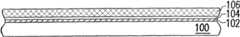
100:基板100: Substrate
102:氮化硅层102: Silicon nitride layer
104:氧化硅层104: silicon oxide layer
106:非晶硅层106: Amorphous silicon layer
108:等离子体处理工艺108: Plasma treatment process
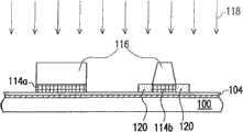
110:激光110: laser
112:扫描方向112: Scan direction
114a、114b:岛状多晶硅层114a, 114b: Island polysilicon layer
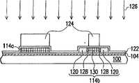
116、124、132:图案化光刻胶层116, 124, 132: patterned photoresist layer
118、126、134:掺杂工艺118, 126, 134: Doping process
120、136:源极/漏极掺杂区120, 136: source/drain doped regions
122:栅极绝缘层122: Gate insulating layer
128:浅掺杂漏极区域128: Shallowly doped drain region
130、138:沟道区130, 138: channel area
140a、140b:栅极140a, 140b: grid
142:层间介电层142: interlayer dielectric layer
144、150:开口144, 150: opening
146:源极/漏极接触金属146: Source/Drain Contact Metal
148:保护层148: protective layer
152:象素电极152: Pixel electrode
具体实施方式Detailed ways
图1A至图1J是依照本发明之一较佳实施例的低温多晶硅(lowtemperature poly-Si,简称LTPS)薄膜晶体管(thin film transistor,简称TFT)的制造工艺剖面图。1A to 1J are cross-sectional views of the manufacturing process of a low temperature polysilicon (low temperature poly-Si, LTPS for short) thin film transistor (thin film transistor, TFT for short) according to a preferred embodiment of the present invention.
请参照图1A,在基板100上先选择性地形成一个缓冲层(bufferlayer),其中缓冲层例如是一氮化硅层102以及一氧化硅层104所组成的堆栈层,其作用在于增进基板100与后续形成的多晶硅层的附着性以及当基板100中有钠等金属离子时,用以防止基板100中的金属离子污染多晶硅层。然后,在氧化硅层104上形成一个非晶硅(amorphous silicon,又称a-Si)层106。Please refer to FIG. 1A , a buffer layer (buffer layer) is selectively formed on the
随后,请参照图1B,进行一个等离子体处理(plasma treatment)工艺108,以调整低温多晶硅薄膜晶体管的激活电压(thresholdvoltage),其中等离子体处理工艺是利用既有的设备如等离子体化学气相沉积(PECVD)机台来进行的工艺,而它例如是使用含氧的等离子体如一氧化二氮等离子体(N2O plasma),以使激活电压往负的方向调整,或者使用含氢的等离子体如氨等离子体(NH3 plasma)或氢等离子体(H2 plasma),以使激活电压往正的方向调整。另外,等离子体处理工艺108更可以通过调整射频电源(RF Power)或工艺时间(process time),以决定激活电压的改变量(shift)大小。Subsequently, referring to FIG. 1B, a plasma treatment (plasma treatment)
接着,请参照图1C,进行一个激光热退火工艺,例如是准分子激光退火工艺(excimer laser annealing,简称ELA),且如图中代表激光110的空白箭头符号及其扫描方向112,以使熔融的非晶硅层106再结晶成为多晶硅层114。Next, referring to FIG. 1C , perform a laser thermal annealing process, such as an excimer laser annealing process (excimer laser annealing, referred to as ELA). The
然后,请参照图1D,图案化多晶硅层114,以形成数个岛状多晶硅层114a、114b。由于多晶硅本身的电子迁移率高,所以通常在进行薄膜晶体管数组的工艺时,可以在显示区外围的周边电路区制作周边电路,如互补式金氧半导体(CMOS),所以之后描述同时形成P型与N型薄膜晶体管的CMOS工艺,其中岛状多晶硅层114a例如是预定形成P型薄膜晶体管的一部份,而岛状多晶硅层114b例如是预定形成N型薄膜晶体管的一部份。但是,本发明并非局限在同时制作P型与N型薄膜晶体管的制造工艺,而仅是以本实施例当作说明本发明特征的一个例子。Then, referring to FIG. 1D , the
之后,请参照图1E,在基板100上形成一个图案化光刻胶层116,以覆盖岛状多晶硅层114a以及部分岛状多晶硅层114b,并暴露出岛状多晶硅层114b两侧上表面。之后,进行一个n+掺杂工艺118,以在岛状多晶硅层114b两侧形成N型薄膜晶体管的源极/漏极掺杂区120。After that, referring to FIG. 1E , a patterned
接着,请参照图1F,去除图案化光刻胶层116,再在岛状多晶硅层114a、114b及氧化硅层104上覆盖一个栅极绝缘层122。然后,在栅极绝缘层122上形成另一个图案化光刻胶层124,以覆盖岛状多晶硅层114a以及部分岛状多晶硅层114b,并暴露出岛状多晶硅层114b中邻近源极/漏极掺杂区120的部位。随后,进行一个n-掺杂工艺126,以形成N型薄膜晶体管的浅掺杂漏极区域128,同时定义出位于浅掺杂漏极区域128之间的沟道区130。Next, referring to FIG. 1F , the patterned
然后,请参照图1G,去除图案化光刻胶层124,再在栅极绝缘层122上形成另一个图案化光刻胶层132,以覆盖岛状多晶硅层114b以及部分岛状多晶硅层114a,并暴露出岛状多晶硅层114b两侧上表面的部位。随后,进行一个p+掺杂工艺134,以形成P型薄膜晶体管的源极/漏极掺杂区136,同时定义出位于源极/漏极掺杂区136之间的沟道区138。Then, referring to FIG. 1G, the patterned
之后,请参照图1H,去除图案化光刻胶层132。随后,可在形成栅极前进行一个活化工艺(activation)。接着,在沟道区138与130上形成栅极140a与140b。然后,在基板100上形成一个层间介电层(inter-layer dielectric,简称ILD)142,以覆盖岛状多晶硅层114a、114b与栅极140a、140b。After that, referring to FIG. 1H , the patterned photoresist layer 132 is removed. Subsequently, an activation process (activation) may be performed before forming the gate. Next,
接着,请参照图1I,在层间介电层142与栅极绝缘层122中形成数个开口144,以暴露出源极/漏极掺杂区136与120,再形成数个源极/漏极接触金属146,源极/漏极接触金属146是通过开口144而与源极/漏极掺杂区136与120电性连接。Next, referring to FIG. 1I,
之后,请参照图1J,在基板100上形成一个保护层148,再在保护层148中形成另一个开口150,以暴露出部分源极/漏极接触金属146,其中保护层146例如氮化硅层。最后,形成一个象素电极152,象素电极152是通过开口150而与源极/漏极接触金属146电性连接,其中象素电极152的材质例如氧化铟锡(ITO)。由于本实施方式是利用既有的设备,去进行能够调整激活电压的等离子体处理工艺,以使薄膜晶体管的激活电压往正或负的方向调整,所以可增加工艺的弹性。After that, referring to FIG. 1J, a
另外,从图1J可观察出本发明的低温多晶硅薄膜晶体管,是至少由岛状多晶硅层114a与114b、栅极140a与140b以及一个栅极绝缘层122所构成。而栅极140a与140b是位于基板100上、岛状多晶硅层114a与114b则位于栅极140a与140b与基板100之间、栅极绝缘层122则配置在栅极140a与140b和岛状多晶硅层114a与114b之间。而且,岛状多晶硅层114a与114b包括一个沟道区138、130以及源/漏极掺杂区域136、120,其中沟道区138、130是位于栅极140a与140b下、源/漏极掺杂区域136、120则位于沟道区138、130两侧。In addition, it can be observed from FIG. 1J that the low temperature polysilicon thin film transistor of the present invention is at least composed of island polysilicon layers 114 a and 114 b ,
此外,以一氧化二氮(N2O)等离子体为例,沟道区138、130中所含的氧(O)浓度(concentration)约在1E19-1E23atoms/cc之间,而氮(N)浓度则约在5E16-1E19atoms/cc之间。而且,本发明的低温多晶硅薄膜晶体管除了实施方式所描述的结构外,亦可应用于其它低温多晶硅薄膜晶体管中,例如是下栅极(bottom gate)型的低温多晶硅薄膜晶体管。In addition, taking nitrous oxide (N2 O) plasma as an example, the concentration of oxygen (O) contained in the
本发明的特点在于利用既有的设备如等离子体化学气相沉积机台,在进行激光热退火工艺之前,对非晶硅层进行等离子体处理工艺,以使薄膜晶体管的激活电压往正或负的方向调整,所以可增进工艺弹性,而不需像习知一定得使用离子植入工艺机台。The feature of the present invention is to use existing equipment such as plasma chemical vapor deposition equipment, before performing the laser thermal annealing process, perform a plasma treatment process on the amorphous silicon layer, so that the activation voltage of the thin film transistor is positive or negative. The direction can be adjusted, so the flexibility of the process can be improved, and it is not necessary to use the ion implantation process machine like the conventional one.
虽然本发明已以较佳实施例披露如上,然其并非用来限定本发明,任何熟悉此技术者,在不脱离本发明的精神和范围内,应该可以作出各种改变与润饰,因此本发明的保护范围应该视后附的权利要求所界定的为准。Although the present invention has been disclosed above with preferred embodiments, it is not intended to limit the present invention. Any skilled person should be able to make various changes and modifications without departing from the spirit and scope of the present invention. Therefore, the present invention The scope of protection should be defined by the appended claims.
Claims (34)
Priority Applications (1)
| Application Number | Priority Date | Filing Date | Title |
|---|---|---|---|
| CNB031223184ACN100555587C (en) | 2003-04-25 | 2003-04-25 | Low-temperature polycrystalline silicon thin film transistor and manufacturing method thereof |
Applications Claiming Priority (1)
| Application Number | Priority Date | Filing Date | Title |
|---|---|---|---|
| CNB031223184ACN100555587C (en) | 2003-04-25 | 2003-04-25 | Low-temperature polycrystalline silicon thin film transistor and manufacturing method thereof |
Publications (2)
| Publication Number | Publication Date |
|---|---|
| CN1540729A CN1540729A (en) | 2004-10-27 |
| CN100555587Ctrue CN100555587C (en) | 2009-10-28 |
Family
ID=34320996
Family Applications (1)
| Application Number | Title | Priority Date | Filing Date |
|---|---|---|---|
| CNB031223184AExpired - LifetimeCN100555587C (en) | 2003-04-25 | 2003-04-25 | Low-temperature polycrystalline silicon thin film transistor and manufacturing method thereof |
Country Status (1)
| Country | Link |
|---|---|
| CN (1) | CN100555587C (en) |
Families Citing this family (4)
| Publication number | Priority date | Publication date | Assignee | Title |
|---|---|---|---|---|
| CN104465319B (en)* | 2014-10-30 | 2017-07-28 | 深圳市华星光电技术有限公司 | The preparation method of low temperature polycrystalline silicon and the preparation method of TFT substrate |
| CN106847824A (en)* | 2015-12-04 | 2017-06-13 | 昆山国显光电有限公司 | Low-temperature polysilicon film transistor and preparation method thereof, AMOLED display panels |
| CN105655355A (en)* | 2016-02-01 | 2016-06-08 | 武汉华星光电技术有限公司 | Manufacturing method of array substrate |
| CN106328586A (en) | 2016-08-24 | 2017-01-11 | 武汉华星光电技术有限公司 | Fabrication method of low temperature poly-silicon array substrate, array substrate and display panel |
Citations (2)
| Publication number | Priority date | Publication date | Assignee | Title |
|---|---|---|---|---|
| JP2001345447A (en)* | 2000-05-31 | 2001-12-14 | Mitsubishi Electric Corp | Thin film transistor, liquid crystal display device, semiconductor device, and manufacturing method thereof |
| CN1396664A (en)* | 1994-09-15 | 2003-02-12 | 株式会社半导体能源研究所 | Manufacturing method of semiconductor device |
- 2003
- 2003-04-25CNCNB031223184Apatent/CN100555587C/ennot_activeExpired - Lifetime
Patent Citations (2)
| Publication number | Priority date | Publication date | Assignee | Title |
|---|---|---|---|---|
| CN1396664A (en)* | 1994-09-15 | 2003-02-12 | 株式会社半导体能源研究所 | Manufacturing method of semiconductor device |
| JP2001345447A (en)* | 2000-05-31 | 2001-12-14 | Mitsubishi Electric Corp | Thin film transistor, liquid crystal display device, semiconductor device, and manufacturing method thereof |
Also Published As
| Publication number | Publication date |
|---|---|
| CN1540729A (en) | 2004-10-27 |
Similar Documents
| Publication | Publication Date | Title |
|---|---|---|
| TWI227565B (en) | Low temperature poly-Si thin film transistor and method of manufacturing the same | |
| US8129232B2 (en) | Semiconductor device and method of manufacturing the same | |
| CN101110429B (en) | Electronic device, display device, image display system and manufacturing method thereof | |
| US11355519B2 (en) | Array substrate, manufacturing method thereof, and display device | |
| JPH05335573A (en) | Thin film semiconductor device | |
| CN100547745C (en) | Low-temperature direct deposition polycrystalline silicon thin film transistor and manufacturing method thereof | |
| US20070176180A1 (en) | Polysilicon structure, thin film transistor panel using the same, and manufacturing method of the same | |
| US10957713B2 (en) | LTPS TFT substrate and manufacturing method thereof | |
| KR100676330B1 (en) | Semiconductor device, method of manufacturing semiconductor device and method of manufacturing thin film transistor | |
| CN101789434B (en) | Image display system and manufacturing method thereof | |
| US20080121892A1 (en) | Low temperature poly silicon liquid crystal display | |
| US7256457B2 (en) | Thin-film transistor device, utilizing different types of thin film transistors | |
| US8603870B2 (en) | Semiconductor device and method of manufacturing the same | |
| JP2000164883A (en) | Manufacture of thin-film insulating gate semiconductor device | |
| JP2006332400A (en) | Thin film semiconductor device and manufacturing method thereof | |
| US6847414B2 (en) | Manufacturing method for liquid crystal display | |
| CN100555587C (en) | Low-temperature polycrystalline silicon thin film transistor and manufacturing method thereof | |
| JP2008047872A (en) | Image display system including thin film transistor device and manufacturing method thereof | |
| CN100369266C (en) | Control thin film transistor, method of manufacturing the same, and electroluminescent display device including the same | |
| CN100426115C (en) | Thin-film transistor array substrate and its making method | |
| JP2009210681A (en) | Display and manufacturing method therefor | |
| TWI229943B (en) | Crystalline silicon TFT panel for LCD or OELD having an LDD region | |
| CN100399507C (en) | Method for manufacturing polycrystalline silicon | |
| JP3084252B2 (en) | Method for manufacturing inverted staggered insulated gate semiconductor device | |
| CN101521219B (en) | Organic electroluminescence display and its manufacturing method |
Legal Events
| Date | Code | Title | Description |
|---|---|---|---|
| C06 | Publication | ||
| PB01 | Publication | ||
| C10 | Entry into substantive examination | ||
| SE01 | Entry into force of request for substantive examination | ||
| C14 | Grant of patent or utility model | ||
| GR01 | Patent grant | ||
| CX01 | Expiry of patent term | ||
| CX01 | Expiry of patent term | Granted publication date:20091028 |