CN100555004C - Optical diffusion module and method for forming optical diffusion structure - Google Patents
Optical diffusion module and method for forming optical diffusion structureDownload PDFInfo
- Publication number
- CN100555004C CN100555004CCNB2006101412108ACN200610141210ACN100555004CCN 100555004 CCN100555004 CCN 100555004CCN B2006101412108 ACNB2006101412108 ACN B2006101412108ACN 200610141210 ACN200610141210 ACN 200610141210ACN 100555004 CCN100555004 CCN 100555004C
- Authority
- CN
- China
- Prior art keywords
- optical
- distance
- module
- adjacent
- pervasion
- Prior art date
- Legal status (The legal status is an assumption and is not a legal conclusion. Google has not performed a legal analysis and makes no representation as to the accuracy of the status listed.)
- Active
Links
Images


Landscapes
- Optical Elements Other Than Lenses (AREA)
Abstract
Translated fromChinese
Description
Translated fromChinese技术领域technical field
本发明涉及一种光学扩散模块,尤其涉及一种通过形成驻波纹形式的微透镜使光线扩散的光学扩散模块。The invention relates to an optical diffusion module, in particular to an optical diffusion module which diffuses light by forming microlenses in the form of standing ripples.
背景技术Background technique
背光模块随着大尺寸化、简单化与低价化的平面显示器市场发展趋势,光源由含汞的CCFL转为固态LED光源或平面光源。提供高效且均匀的背光源,微光学结构膜片起着极为重要的作用。对于成本与效能而言,微结构光学膜片可以提供较低的材料成本与较佳的光学效能,因此,以微结构进行背光源扩散的光学设计颇多,对于点光源或线光源可以看到以单轴向或双轴向的方式来达到扩散的效果。Backlight Module With the development trend of the large-sized, simplified and low-cost flat-panel display market, the light source has changed from mercury-containing CCFL to solid-state LED light source or flat light source. To provide an efficient and uniform backlight, the micro-optical structure diaphragm plays an extremely important role. In terms of cost and performance, microstructured optical films can provide lower material costs and better optical performance. Therefore, there are many optical designs for backlight diffusion with microstructures. For point light sources or line light sources, it can be seen The effect of diffusion is achieved in a uniaxial or biaxial manner.
背光模块或一般灯管照明中冷阴极光源或日光灯管的使用需要使用重金属汞来产生光色,这在环保上将逐渐受到限制。LED的光源是亮度与日剧增、寿命长、低耗电、无污染的固态光源,因此LED应用的范围不断扩大,从一般照明到显示器背光源的使用,目前LED应用在显示器上主要是在3C电子用品,日韩各大厂将LED应用推向大尺寸的平面显示器中,LED色彩饱和度佳,可以用RGB混光或蓝光搭配荧光的方式提供白光光源,在制造过程中可以配合电路进行光源的设计调控,但与冷阴极灯管相比,其单价高,存在色温问题,这些都是极待解决的课题。目前利用单颗光学帽与阵列的方式可以达到局部混光效果,扩散设计多半是以传统的扩散厚板来进行,如何使LED光源分布更均匀、降低LED使用颗数、减少背光模块的厚度、利用有效的微光学结构膜片、均匀分散点光源是本发明的重要出发点。The use of cold cathode light sources or fluorescent tubes in backlight modules or general lamp lighting requires the use of heavy metal mercury to produce light color, which will gradually be restricted in terms of environmental protection. The light source of LED is a solid-state light source with increased brightness and daily increase, long life, low power consumption, and no pollution. Therefore, the scope of LED application continues to expand, from general lighting to the use of display backlight. At present, LED applications are mainly in the display. For 3C electronic products, major manufacturers in Japan and South Korea push LED applications to large-size flat-panel displays. LEDs have good color saturation and can provide white light sources in the form of RGB mixed light or blue light with fluorescent light. The design and control of the light source, but compared with the cold-cathode lamp, its unit price is high, and there is a problem of color temperature. These are issues that need to be solved. At present, the local mixing effect can be achieved by using a single optical cap and an array. The diffusion design is mostly carried out with the traditional thick diffusion plate. How to make the LED light source distribution more uniform, reduce the number of LEDs used, and reduce the thickness of the backlight module. Utilizing an effective micro-optical structure diaphragm to uniformly disperse point light sources is an important starting point of the present invention.
一般而言,传统的直下式光源扩散目前最常见的处理方式是采用扩散板(膜),以雾化扩散的方式将光源均匀分散,这种方式存在一些问题。由于采用混成雾化厚板将导致辉度降低和光源被材料吸收损耗,混成粒子扩散采用散射的方式,扩散的角度不大也无法控制。另一种方式是采取柱型镜阵列结构,利用微结构几何光学的原理,以膜片就可达到较高的辉度和可控制的扩散角度,配合一片扩散膜或雾化处理面就可以达到均匀化的效果。一般制作柱型镜的方式不外乎采用机械加工、热融法或其它复合方式来成型,柱型镜阵列间的间隙处理、机械强度与复制性也是很重要的。针对如何运用特殊的光学设计与简化的制造过程制作出无间隙、高机械强度及高结构复制性的高分子微结构光学膜片的问题,本发明的发明人曾在专利申请号为CN 94133325和CN 94133326的两份发明专利申请中披露了以特殊的光罩制造出连续波纹状微结构阵列的方法和所制造出的微结构阵列。Generally speaking, the most common way to deal with the traditional direct-type light source diffusion is to use a diffuser plate (film) to evenly disperse the light source by means of atomization and diffusion. There are some problems in this way. Since the use of a hybrid atomized thick plate will lead to a decrease in luminance and a loss of light source being absorbed by the material, the diffusion of the hybrid particles adopts a scattering method, and the diffusion angle is not large and cannot be controlled. Another way is to adopt a cylindrical mirror array structure, and use the principle of microstructure geometric optics to achieve high luminance and controllable diffusion angle with a diaphragm, which can be achieved with a diffusion film or an atomized surface. Homogenization effect. Generally, the method of manufacturing cylindrical mirrors is nothing more than machining, thermal melting or other composite methods. The gap between the cylindrical mirror arrays, mechanical strength and replicability are also very important. Aiming at the problem of how to use special optical design and simplified manufacturing process to make a macromolecule microstructure optical film with no gap, high mechanical strength and high structural reproducibility, the inventor of the present invention once applied for the patent application number CN 94133325 and The two invention patent applications of CN 94133326 disclosed a method for manufacturing a continuous corrugated microstructure array with a special mask and the manufactured microstructure array.
所述两份专利申请披露了利用激光拖拉法并结合光罩图形设计制造出供制造微透镜使用的模具的方案。如图1A所示,激光束B经由光罩5照射至基材10上,同时将光罩5朝L1的方向拖拉,如此,激光束可在基材10上刻写出沟槽12。所述两个技术方案主要是控制激光能量束在基材上不同位置的蚀刻量,以造成灰阶渐增效果而产生三维结构。其中,激光拖拉可控制的参数包括拖拉速度、激光能量、及重复频率等,此部分最主要影响整体结构的深度,例如拖拉速度愈快、激光能量愈小或激光重复频率愈小使得单位时间内的蚀刻量愈小,造成结构的整体深度较浅;反之,则较深。另一方面,光罩图形是影响三维结构轮廓最主要的控制因素,如图1B所示,在光罩M30上形成凹凸状的图形M3,然后通过激光束的照射在基材上形成凹凸状交错排列的第一微透镜202以及第二微透镜204,借助于光罩图形M3中央与两侧开口面积的不同,造成两个不同位置蚀刻量的差异,进而产生不同的深度。在所述两种方案中,主要利用了不同长短轴椭圆形或圆形的光罩图形矩阵组合,其中,椭圆形光罩长短轴比例愈大,造成蚀刻量差异愈大,而形成曲率较小的椭圆曲线,若选用圆形光罩则形成近似圆形的曲面。The two patent applications disclose the scheme of manufacturing the mold used for manufacturing the microlens by using the laser dragging method combined with the pattern design of the mask. As shown in FIG. 1A , the laser beam B is irradiated onto the substrate 10 through the mask 5 , and at the same time the mask 5 is pulled toward the direction L1 , so that the laser beam can write the groove 12 on the substrate 10 . The two technical solutions are mainly to control the etching amount of the laser energy beam at different positions on the substrate, so as to cause the effect of increasing the gray scale to produce a three-dimensional structure. Among them, the controllable parameters of laser dragging include dragging speed, laser energy, and repetition rate, etc. This part mainly affects the depth of the overall structure. The smaller the amount of etching, the shallower the overall depth of the structure; otherwise, the deeper. On the other hand, the mask pattern is the most important controlling factor affecting the three-dimensional structure profile. As shown in FIG. 1B, a concave-convex pattern M3 is formed on the mask M30, and then a concave-convex pattern is formed on the substrate by laser beam irradiation. The arrangement of the
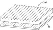
图2A示出了将图1B所示的光扩散用的微透镜结构200与扩散膜50配合使用的情况,图2B是借助于微透镜结构200所扩散的光的照度分布图,图中的长条状区域表示光线汇聚处。2A shows the situation that the
发明内容Contents of the invention
背景技术中所提到的微透镜结构可使光线一维扩散,本发明的目的在于提供一种光扩散结构,其可以达到使光二维扩散的效果。此外,本发明还将提供一种光扩散结构的形成方法。The microlens structure mentioned in the background art can diffuse light one-dimensionally. The purpose of the present invention is to provide a light diffusion structure that can achieve the effect of two-dimensional light diffusion. In addition, the present invention will also provide a method for forming the light diffusion structure.
为实现所述目的,本发明一优选实施方式的光扩散模块包括一扩散板以及一光扩散结构,扩散板具有一第一面,光扩散结构形成于第一面上。光扩散结构包括:多个突起部以及多个凹陷部,所述突起部沿第一方向以及第二方向排列成一个二维的阵列,所述凹陷部沿第一方向以及第二方向排列成一个二维的阵列。每一突起部相邻于多个凹陷部,每一凹陷部相邻于多个突起部,所述突起部、凹陷部以及突起部与凹陷部的相邻处的曲率皆不为零。To achieve the above object, a light diffusion module according to a preferred embodiment of the present invention includes a diffusion plate and a light diffusion structure, the diffusion plate has a first surface, and the light diffusion structure is formed on the first surface. The light diffusion structure includes: a plurality of protrusions and a plurality of depressions, the protrusions are arranged in a two-dimensional array along the first direction and the second direction, and the depressions are arranged in a two-dimensional array along the first direction and the second direction two-dimensional array. Each protrusion is adjacent to a plurality of depressions, each depression is adjacent to a plurality of protrusions, and the curvatures of the protrusions, the depressions, and adjacent positions between the protrusions and the depressions are not zero.
在所述优选实施方式中,沿第一方向,任意两突起部之间的距离可以相等或不相等;沿第二方向,任意两突起部之间的距离可以相等或不相等。In the preferred embodiment, along the first direction, the distance between any two protrusions may be equal or unequal; along the second direction, the distance between any two protrusions may be equal or unequal.
同样,在所述优选实施方式中,沿第一方向,任意两凹陷部之间的距离可以相等或不相等;沿第二方向,任意两凹陷部之间的距离可以相等或不相等。Likewise, in the preferred embodiment, along the first direction, the distance between any two concave parts may be equal or unequal; along the second direction, the distance between any two concave parts may be equal or unequal.
本发明还提供一种光扩散结构的形成方法,包括下列步骤:提供基材;提供光罩,该光罩具有多个通孔,这些通孔排列成阵列;提供能量束;将光罩置于能量束与基材之间;于第一方向上移动光罩或基材;以及于第二方向上移动光罩或基材,通过能量束的光线经由光罩在基材上形成多个相邻的突出部与凹陷部,使这些突出部与凹陷部形成二维阵列。The present invention also provides a method for forming a light diffusion structure, comprising the following steps: providing a substrate; providing a photomask, the photomask has a plurality of through holes arranged in an array; providing an energy beam; placing the photomask on between the energy beam and the substrate; moving the mask or the substrate in the first direction; and moving the mask or the substrate in the second direction, the light rays passing through the energy beam pass through the mask to form a plurality of adjacent Protrusions and depressions, so that these protrusions and depressions form a two-dimensional array.
附图说明Description of drawings
为使本发明的所述和其它目的、特征、和优点更明显易懂,下文特举优选实施方式并结合附图对本发明进行详细说明。In order to make the above and other objects, features, and advantages of the present invention more comprehensible, preferred embodiments are exemplified below and the present invention is described in detail with reference to the accompanying drawings.
图1A为利用激光拖拉法制造微透镜结构的示意图;Fig. 1A is the schematic diagram that utilizes laser dragging method to manufacture microlens structure;
图1B为激光拖拉法的光罩及所制造出的微透镜结构的立体图;FIG. 1B is a perspective view of a photomask and a manufactured microlens structure of the laser dragging method;
图2A为图1B所制造出的微透镜结构的实际应用的示意图;FIG. 2A is a schematic diagram of the practical application of the microlens structure manufactured in FIG. 1B;
图2B为通过图2A所示的微透镜结构所扩散的光的照度分布图;Fig. 2B is the illuminance distribution diagram of the light diffused by the microlens structure shown in Fig. 2A;
图3为借助于激光拖拉法并配合光罩来制造本发明的光扩散结构的示意图;3 is a schematic diagram of manufacturing the light diffusion structure of the present invention by means of a laser dragging method and cooperating with a photomask;
图4为使用图3所示的方法所制造出的光学扩散模块的示意图;FIG. 4 is a schematic diagram of an optical diffusion module manufactured by the method shown in FIG. 3;
图5为本发明的光扩散结构的一实施方式的照度分布图;5 is an illumination distribution diagram of an embodiment of the light diffusion structure of the present invention;
图6为本发明的光扩散结构的另一实施方式的照度分布图;6 is an illumination distribution diagram of another embodiment of the light diffusion structure of the present invention;
图7为本发明的光扩散结构的又一实施方式的照度分布图;7 is an illumination distribution diagram of another embodiment of the light diffusion structure of the present invention;
图8为本发明的光扩散结构的再一实施方式的照度分布图;Fig. 8 is an illuminance distribution diagram of another embodiment of the light diffusion structure of the present invention;
图9为本发明的光扩散结构配合扩散膜使用的示意图;9 is a schematic diagram of the use of the light diffusion structure of the present invention in conjunction with a diffusion film;
图10为本发明的光扩散结构配合颗粒状结构使用的示意图;Fig. 10 is a schematic diagram of the use of the light diffusion structure of the present invention in conjunction with the granular structure;
图11为使用具有光扩散效果的高分子材料所制造的扩散板的示意图。FIG. 11 is a schematic diagram of a diffuser plate manufactured by using a polymer material with a light-diffusing effect.
附图标记说明Explanation of reference signs
5 光罩5 Mask
10 基材10 Substrate
12 沟槽12 Groove
50 扩散膜50 Diffusion film
120 第一沟槽120 The first groove
140 第二沟槽140 Second groove
200 微透镜结构200 microlens structure
202 第一微透镜202 The first microlens
204 第二微透镜204 Second Microlens
500 光扩散结构500 Light Diffusion Structure
600、700、800、900 光学扩散模块600, 700, 800, 900 Optical Diffusion Module
620 扩散板620 diffuser plate
621 表面(第一面)621 Surface (first side)
622 底面(第二面)622 Bottom (second side)
640 光扩散结构640 Light Diffusion Structure
660 突起部660 Protrusions
680 凹陷部680 Depression
B 激光束B Laser Beam
D1、D2 两相邻突起部之间的距离D1, D2 The distance between two adjacent protrusions
D3、D4 两相邻凹陷部之间的距离D3, D4 The distance between two adjacent depressions
M3 图形M3 Graphics
M30 光罩M30 Mask
L1 第一方向L1 First Direction
L2 第二方向L2 Second direction
具体实施方式Detailed ways
本发明的光扩散结构主要是以背景技术中所述的激光拖拉法配合光罩在基材上形成驻波纹状的结构,以达到使光二维扩散的效果。以下分别说明如何以激光拖拉法制造驻波纹状的光扩散结构以及所制造出的光扩散结构。The light diffusion structure of the present invention is mainly to form a standing corrugated structure on the base material by using the laser dragging method described in the background art with a photomask, so as to achieve the effect of two-dimensional light diffusion. How to manufacture the standing corrugated light-diffusing structure and the manufactured light-diffusing structure by the laser dragging method are described below.
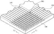
图3为借助于激光拖拉法并配合光罩来制造本发明的光扩散结构的示意图。与图1A类似,利用光罩(未示出)沿第一方向L1移动,同时以激光束照射形成多个第一沟槽120,然后将光罩沿第二方向L2移动,并照射激光而形成多个第二沟槽140,如此第一沟槽120与第二沟槽140重叠的部分就形成了驻波纹状的光扩散结构500。FIG. 3 is a schematic diagram of manufacturing the light diffusion structure of the present invention by means of a laser dragging method and matching with a photomask. Similar to FIG. 1A, a plurality of
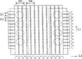
图4示出了使用图3所示的方法制造的光学扩散模块600。光学扩散模块600包括扩散板620以及光扩散结构640。光扩散结构640包括多个突起部660以及多个凹陷部680,突起部660沿第一方向L1与第二方向L2排列成二维的阵列,同样,凹陷部680也沿第一方向L1以及第二方向L2排列成二维的阵列,突起部660与凹陷部680彼此交错排列(即,一列突起部660邻接于一列凹陷部680)而形成驻波纹状。在本实施方式中,每一突起部660邻接于四个凹陷部680,而每一凹陷部680邻接于四个突起部660,通过光罩的设计(如背景技术所述)使突起部660、凹陷部680以及突起部660与凹陷部680邻接处的曲率皆不为0。在第一方向L1上,两相邻突起部660之间的距离为D1,两相邻凹陷部680之间的距离为D3。在第二方向L2上,两相邻突起部660之间的距离为D2,两相邻凹陷部680之间的距离为D4。FIG. 4 shows an
在图4中D1=D2且D3=D4,但是D1、D2、D3及D4可以有多种组合,以下分别以照度分布图进行说明。In FIG. 4 , D1 = D2 and D3 = D4 , but D1 , D2 , D3 and D4 can be combined in various ways, which will be described with illuminance distribution diagrams below.
图5为本发明的光扩散结构的一实施方式的照度分布图。其中,在第一方向L1上,任意两突起部660之间的距离D1均相等,且任意两凹陷部680之间的距离D3均相等,在第二方向L2上,任意两突起部660之间的距离D2均相等,且任意两凹陷部680之间的距离D4均相等。Fig. 5 is an illuminance distribution diagram of an embodiment of the light diffusion structure of the present invention. Wherein, in the first direction L1, the distance D1 between any two
图6为本发明的光扩散结构的另一实施方式的照度分布图。其中,在第一方向L1上,任意两突起部660之间的距离D1均相等,且任意两凹陷部680之间的距离D3均相等,在第二方向L2上,任意两突起部660之间的距离D2不相等,且任意两凹陷部680之间的距离D4不相等,D2及D4在中央部分最小,而从中央向两侧逐渐增大,然后再逐渐变小。FIG. 6 is an illumination distribution diagram of another embodiment of the light diffusion structure of the present invention. Wherein, in the first direction L1, the distance D1 between any two
图7为本发明的光扩散结构的又一实施方式的照度分布图。其中,在第一方向L1上,任意两突起部660之间的距离D1均相等,且任意两凹陷部680之间的距离D3均相等,在第二方向L2上,任意两突起部660之间的距离D2不相等,且任意两凹陷部680之间的距离D4不相等,D2及D4在中央部分最大,而从中央向两侧逐渐增小。Fig. 7 is an illumination distribution diagram of another embodiment of the light diffusion structure of the present invention. Wherein, in the first direction L1, the distance D1 between any two
图8为本发明的光扩散结构的再一实施方式的照度分布图。其中,在第一方向L1上,任意两突起部660之间的距离D1不相等,且任意两凹陷部680之间的距离D3不相等,D1及D3在中央部分最小,而从中央向两侧逐渐增大,然后再逐渐变小。在第二方向L2上,任意两突起部660之间的距离D2不相等,且任意两凹陷部680之间的距离D4不相等,D2及D4在中央部分最小,而从中央向两侧逐渐增大,然后再逐渐变小。FIG. 8 is an illumination distribution diagram of still another embodiment of the light diffusion structure of the present invention. Wherein, in the first direction L1, the distance D1 between any two
所述各实施方式仅是多种组合中的几种,以此为例进行说明,当然本发明并不限于此,例如在第一方向L1上,任意两突起部660之间的距离D1可以不相等,但任意两凹陷部680之间的距离D3相等。The above-mentioned implementations are only a few of the various combinations, which are taken as an example for illustration. Of course, the present invention is not limited thereto. For example, in the first direction L1, the distance D1 between any two
另外,在所述各实施方式中,虽然第一方向L1与第二方向L2正交,但是第一方向L1与第二方向L2也可不正交,而不以此为限制。In addition, in each of the above-described embodiments, although the first direction L1 and the second direction L2 are orthogonal, the first direction L1 and the second direction L2 may not be orthogonal, and this is not a limitation.
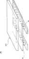
再者,本发明的扩散板620也可以和传统的扩散膜50结合使用形成光学扩散模块700,如图9所示,图中30为LED阵列模块。或者在扩散板620的底面(第二面)622{光扩散结构600形成于表面(第一面)621}形成颗粒状结构或对底面622进行雾化处理,可加强光扩散效果,如图10所示的光学扩散模块800。此外,也可用具有光扩散效果的高分子材料形成扩散板620,如图11所示的光学扩散模块900。Furthermore, the
虽然已通过优选实施方式对本发明披露于上,但这并非是对本发明的限制,本领域任何技术人员在不超出本发明的构思和范围的前提下,可作出一些变换与润饰,因此本发明的保护范围应以所附权利要求界定的范围为准。Although the present invention has been disclosed above through preferred embodiments, this is not a limitation of the present invention. Any skilled person in the art can make some changes and modifications without departing from the concept and scope of the present invention. Therefore, the present invention The scope of protection should be defined by the appended claims.
Claims (33)
Priority Applications (1)
| Application Number | Priority Date | Filing Date | Title |
|---|---|---|---|
| CNB2006101412108ACN100555004C (en) | 2006-09-28 | 2006-09-28 | Optical diffusion module and method for forming optical diffusion structure |
Applications Claiming Priority (1)
| Application Number | Priority Date | Filing Date | Title |
|---|---|---|---|
| CNB2006101412108ACN100555004C (en) | 2006-09-28 | 2006-09-28 | Optical diffusion module and method for forming optical diffusion structure |
Publications (2)
| Publication Number | Publication Date |
|---|---|
| CN101153924A CN101153924A (en) | 2008-04-02 |
| CN100555004Ctrue CN100555004C (en) | 2009-10-28 |
Family
ID=39255679
Family Applications (1)
| Application Number | Title | Priority Date | Filing Date |
|---|---|---|---|
| CNB2006101412108AActiveCN100555004C (en) | 2006-09-28 | 2006-09-28 | Optical diffusion module and method for forming optical diffusion structure |
Country Status (1)
| Country | Link |
|---|---|
| CN (1) | CN100555004C (en) |
Families Citing this family (7)
| Publication number | Priority date | Publication date | Assignee | Title |
|---|---|---|---|---|
| CN101539267B (en)* | 2008-03-20 | 2012-11-21 | 香港理工大学 | High-power LED street lamp cap of free-form surface lens light distribution |
| KR101034479B1 (en)* | 2008-07-07 | 2011-05-17 | 도레이첨단소재 주식회사 | Thin Film Transistor Liquid Crystal Display Optical Sheet for Backlight Unit and Thin Film Transistor Liquid Crystal Display |
| TWI418855B (en) | 2008-08-28 | 2013-12-11 | Ind Tech Res Inst | Illuminant module with an optical film of multiple curvatures |
| CN101684916B (en)* | 2008-09-22 | 2012-05-30 | 财团法人工业技术研究院 | Variable Curvature Optical Module |
| CN104819434B (en)* | 2015-04-16 | 2018-12-14 | 宁波江北激智新材料有限公司 | A kind of even smooth film and lighting apparatus and display device backlight using the even smooth film |
| CN104914490B (en)* | 2015-07-03 | 2017-10-27 | 宁波江北激智新材料有限公司 | A kind of even smooth film and its use equipment |
| US9983469B2 (en)* | 2016-06-21 | 2018-05-29 | Casio Computer Co., Ltd. | Light source unit and projector having the same light source unit |
Citations (2)
| Publication number | Priority date | Publication date | Assignee | Title |
|---|---|---|---|---|
| CN1539085A (en)* | 2001-08-03 | 2004-10-20 | 3M创新有限公司 | Optical film containing microreplicated structures and method of making the same |
| JP2005227407A (en)* | 2004-02-10 | 2005-08-25 | Daicel Chem Ind Ltd | Anti-glare sheet |
- 2006
- 2006-09-28CNCNB2006101412108Apatent/CN100555004C/enactiveActive
Patent Citations (2)
| Publication number | Priority date | Publication date | Assignee | Title |
|---|---|---|---|---|
| CN1539085A (en)* | 2001-08-03 | 2004-10-20 | 3M创新有限公司 | Optical film containing microreplicated structures and method of making the same |
| JP2005227407A (en)* | 2004-02-10 | 2005-08-25 | Daicel Chem Ind Ltd | Anti-glare sheet |
Also Published As
| Publication number | Publication date |
|---|---|
| CN101153924A (en) | 2008-04-02 |
Similar Documents
| Publication | Publication Date | Title |
|---|---|---|
| CN100555004C (en) | Optical diffusion module and method for forming optical diffusion structure | |
| TWI295355B (en) | Optical diffusion module and method of manufacturing optical diffusion structure | |
| JP5134202B2 (en) | LED light source | |
| TWI301533B (en) | Optical diffusion module | |
| CN101135738A (en) | Optical Diffusion Module | |
| CN109164638B (en) | Light emitting module, manufacturing method thereof and direct type backlight source | |
| CN102472844B (en) | Optical sheet | |
| CN101097349A (en) | Backlight assembly and liquid crystal display device using same | |
| KR100682483B1 (en) | Flat light source device | |
| TWI460480B (en) | Light guide plate for plane light source, method for manufacturing the same, and plane light source unit using the same | |
| US7470038B2 (en) | Diffuser having optical structures | |
| CN109031510B (en) | A light guide plate and its manufacturing method, a backlight module and a display device | |
| CN101373234A (en) | Backlight module and its optical film | |
| CN110701504A (en) | Lamp strip structure | |
| TWI735126B (en) | Electronic apparatus and manufacturing method thereof | |
| TWI507786B (en) | Display apparatus and side edge type backlight module thereof | |
| WO2007064133A1 (en) | Light guiding panel using point lights and fabricating method thereof | |
| JP5272508B2 (en) | Optical sheet, backlight unit and display device | |
| CN219039406U (en) | Light guide plate and light guide film | |
| TWI723563B (en) | Light bar structure | |
| US7878682B2 (en) | Mixed light apparatus | |
| TWI417573B (en) | Brightening the diffusion film | |
| CN103375711A (en) | Diffusion structure and device with light source using same | |
| JP4909287B2 (en) | Light diffusion module | |
| CN201096908Y (en) | Optical diffusion assembly |
Legal Events
| Date | Code | Title | Description |
|---|---|---|---|
| C06 | Publication | ||
| PB01 | Publication | ||
| C10 | Entry into substantive examination | ||
| SE01 | Entry into force of request for substantive examination | ||
| C14 | Grant of patent or utility model | ||
| GR01 | Patent grant |