CN100543864C - Stacked semiconductor memory device - Google Patents
Stacked semiconductor memory deviceDownload PDFInfo
- Publication number
- CN100543864C CN100543864CCNB2005100810298ACN200510081029ACN100543864CCN 100543864 CCN100543864 CCN 100543864CCN B2005100810298 ACNB2005100810298 ACN B2005100810298ACN 200510081029 ACN200510081029 ACN 200510081029ACN 100543864 CCN100543864 CCN 100543864C
- Authority
- CN
- China
- Prior art keywords
- memory cell
- input
- memory
- cell array
- output
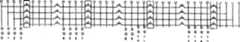
- Prior art date
- Legal status (The legal status is an assumption and is not a legal conclusion. Google has not performed a legal analysis and makes no representation as to the accuracy of the status listed.)
- Expired - Fee Related
Links
Images


Classifications
- G—PHYSICS
- G11—INFORMATION STORAGE
- G11C—STATIC STORES
- G11C5/00—Details of stores covered by group G11C11/00
- G11C5/02—Disposition of storage elements, e.g. in the form of a matrix array
- G11C5/025—Geometric lay-out considerations of storage- and peripheral-blocks in a semiconductor storage device
- G—PHYSICS
- G11—INFORMATION STORAGE
- G11C—STATIC STORES
- G11C5/00—Details of stores covered by group G11C11/00
- G11C5/02—Disposition of storage elements, e.g. in the form of a matrix array
- G—PHYSICS
- G11—INFORMATION STORAGE
- G11C—STATIC STORES
- G11C5/00—Details of stores covered by group G11C11/00
- G11C5/06—Arrangements for interconnecting storage elements electrically, e.g. by wiring
- G11C5/063—Voltage and signal distribution in integrated semi-conductor memory access lines, e.g. word-line, bit-line, cross-over resistance, propagation delay
Landscapes
- Engineering & Computer Science (AREA)
- Microelectronics & Electronic Packaging (AREA)
- Dram (AREA)
- Semiconductor Memories (AREA)
Abstract
Translated fromChinese
Description
Translated fromChinese技术领域technical field
本发明涉及半导体存储器器件,更具体地,涉及其中存储单元阵列芯片和用于改变存储器配置的接口芯片被堆叠在一起的半导体存储器器件。The present invention relates to a semiconductor memory device, and more particularly, to a semiconductor memory device in which a memory cell array chip and an interface chip for changing a memory configuration are stacked together.
背景技术Background technique
随着半导体集成电路的小型化和集成度增加,DRAM(动态随机存取存储器)和SRAM(静态随机存取存储器)的容量已经大大增加。然而,半导体的小型化存在限制,并且因此需要引入新的技术来获得容量的更大增加。As the miniaturization and integration of semiconductor integrated circuits have increased, the capacity of DRAM (Dynamic Random Access Memory) and SRAM (Static Random Access Memory) has greatly increased. However, there is a limit to the miniaturization of semiconductors, and thus it is necessary to introduce new technologies to obtain a greater increase in capacity.
已经提出了其中半导体芯片被堆叠起来的三维半导体,作为一种获得更大容量的技术。日本专利未审公开No.H04-196263公开了其中半导体芯片被堆叠起来而不改变芯片面积的大规模集成电路的实现。在这种电路中,存储器电路被集成在分离的芯片上,而该芯片则被堆叠在主半导体集成电路上。日本专利未审公开No.2002-26283和日本专利未审公开No.2003-209222公开了多层存储器结构,其中使用多层来实现存储单元阵列,以获得更大的容量增长。A three-dimensional semiconductor in which semiconductor chips are stacked has been proposed as a technique for achieving a larger capacity. Japanese Patent Laid-Open No. H04-196263 discloses the realization of a large-scale integrated circuit in which semiconductor chips are stacked without changing the chip area. In such a circuit, a memory circuit is integrated on a separate chip which is stacked on a main semiconductor integrated circuit. Japanese Patent Laid-Open Publication No. 2002-26283 and Japanese Patent Laid-Open Publication No. 2003-209222 disclose a multi-layer memory structure in which a memory cell array is implemented using multiple layers to achieve greater capacity growth.
在日本未审公开No.2002-026283中所描述的发明中,并不是为多层存储器芯片中的每一个存储器芯片提供存储器外围电路,而是每个存储器芯片共享一对外围电路,以实现占用芯片面积的外围电路面积的减小。In the invention described in Japanese Unexamined Publication No. 2002-026283, instead of providing a memory peripheral circuit for each memory chip in the multilayer memory chip, each memory chip shares a pair of peripheral circuits to achieve occupation The chip area is reduced by the peripheral circuit area.
在日本专利未审公开No.2003-209222中所描述的发明中,在制造多层存储器器件之后,可以对存储器层进行分拣,以使得能够去除有缺陷的存储器层。In the invention described in Japanese Patent Laid-Open Publication No. 2003-209222, after manufacturing a multilayer memory device, memory layers may be sorted so that defective memory layers can be removed.
然而,虽然上述多层存储器器件中每一个都实现了有限芯片面积内存储器容量的增加,但是这些公开都没有涉及作为存储器组成元件的输入/输出位数以及存储体数目,或者这些公开都没有涉及数据传输速率。However, although each of the above-mentioned multilayer memory devices achieves an increase in memory capacity within a limited chip area, none of these disclosures deals with the number of input/output bits and the number of banks as constituent elements of the memory, or none of these disclosures deals with data transfer rate.
另一方面,随着存储器性能的增长,CPU的性能增长不仅需要更大容量的存储器器件,还需要输入/输出位的增加、存储体数目的增加以及更高的存储器传输速率。系统的多样化导致了多种存储器配置,结果,必须开发许多种类的存储器器件,并且开发这些存储器器件的成本逐年增长。On the other hand, with the growth of memory performance, the performance growth of CPU requires not only a larger memory device, but also an increase in input/output bits, an increase in the number of memory banks, and a higher memory transfer rate. The diversification of systems leads to various memory configurations, and as a result, many kinds of memory devices must be developed, and the cost of developing these memory devices is increasing year by year.
发明内容Contents of the invention
做出本发明是为了解决这些因素,并且本发明的目的在于提供一种堆叠式半导体存储器器件,其中存储单元阵列和用于改变存储单元阵列的电路被堆叠在分离的芯片上,并且然后使用多条小延迟的接线将这些芯片互连起来;这样,这种堆叠式半导体存储器器件实现了存储器配置的更大范围的重配置,尤其是输入/输出位配置和与存储器传输速率相关的输入/输出预取配置,并且允许了开发多种存储器器件的成本降低。The present invention has been made to solve these factors, and an object of the present invention is to provide a stacked semiconductor memory device in which a memory cell array and a circuit for changing the memory cell array are stacked on separate chips, and then multiple A wire with a small delay interconnects these chips; in this way, this stacked semiconductor memory device realizes a wider range of reconfiguration of the memory configuration, especially the I/O bit configuration and the I/O associated with the memory transfer rate prefetch configuration and allows for cost reduction in the development of a wide variety of memory devices.
本发明的堆叠式半导体存储器器件包括:存储单元阵列芯片,其具有存储单元阵列;与存储单元阵列芯片堆叠在一起的接口芯片,其具有用于改变存储单元阵列的输入/输出位配置的存储器配置切换电路;和用于连接存储单元阵列芯片和接口芯片的多条芯片间接线。The stacked semiconductor memory device of the present invention includes: a memory cell array chip having a memory cell array; an interface chip stacked with the memory cell array chip having a memory configuration for changing an input/output bit configuration of the memory cell array a switching circuit; and a plurality of inter-chip wires for connecting the memory cell array chip and the interface chip.
在这种情形中,多个存储单元阵列芯片可以被堆叠在一起,并且存储器配置切换电路可以改变设置在所述堆叠在一起的多个存储单元阵列芯片中的每一个芯片上的存储单元阵列的输入/输出位配置。In this case, a plurality of memory cell array chips may be stacked, and the memory configuration switching circuit may change the configuration of the memory cell array provided on each of the stacked plurality of memory cell array chips. Input/Output bit configuration.
另外,存储器配置切换电路可以包括:针对每一组指定数目的组成存储单元阵列的多个存储器单元而设置的多个开关,其中每个存储器单元组的输入/输出位数根据这些开关的开关状态改变;和位切换电路,用于通过切换多个开关的开关状态,来改变相应的存储器单元组的输入/输出位数。In addition, the memory configuration switching circuit may include a plurality of switches provided for each group of a specified number of memory cells constituting the memory cell array, wherein the number of input/output bits of each memory cell group depends on the switching states of the switches changing; and a bit switching circuit for changing the input/output bit number of the corresponding memory cell group by switching the switching states of the plurality of switches.
在这种情形中,存储器配置切换电路可以包括:多个锁存电路,每一个锁存电路都连接到多条数据总线中各自的一条,以便锁存每条数据总线中的数据,多个存储器单元组的输入/输出数据的输入和输出经过这些数据总线;和控制电路,用于通过控制多个锁存电路中的锁存定时来控制输入/输出数据的位数和传输速率。In this case, the memory configuration switching circuit may include a plurality of latch circuits each connected to a respective one of the plurality of data buses to latch data in each data bus, the plurality of memory input/output of cell group input/output data via these data buses; and a control circuit for controlling the number of bits and transfer rate of input/output data by controlling latch timing in a plurality of latch circuits.
另外,控制电路可以利用位切换电路来改变存储器单元组的输入/输出位数,并且可以实现控制,从而使存储器单元组的输入/输出位数等于输入/输出数据的位数。In addition, the control circuit can change the number of input/output bits of the memory cell group by using the bit switching circuit, and can implement control so that the number of input/output bits of the memory cell group is equal to the number of bits of input/output data.
另外,控制电路可以配备有安装在接线中的熔丝,并且根据这些熔丝的切断状态,可以生成用于控制存储器单元组的输入/输出位数的信号,或者可以控制输入/输出数据的位数及传输速率。In addition, the control circuit may be equipped with fuses installed in the wiring, and according to the cut state of these fuses, a signal for controlling the number of input/output bits of the memory cell group may be generated, or the bit of input/output data may be controlled number and transfer rate.
另外,控制电路可以是根据焊接选项输入信号的组合进行操作的逻辑电路,并且可以生成用于控制存储器单元组的输入/输出位数或者输入/输出数据位数及传输速率的信号。根据上述任何描述的堆叠式半导体存储器器件可以是DRAM。In addition, the control circuit may be a logic circuit that operates according to a combination of welding option input signals, and may generate signals for controlling the number of input/output bits of the memory cell group or the number of input/output data bits and the transfer rate. A stacked semiconductor memory device according to any of the above descriptions may be a DRAM.
根据本发明,在其中存储单元阵列芯片和接口芯片被堆叠在一起的存储器器件中,通过接口芯片的存储器配置切换电路来改变存储单元阵列芯片的输入/输出位配置以及数据传输速率。这样,可以减少开发多种存储器器件的成本。According to the present invention, in a memory device in which a memory cell array chip and an interface chip are stacked, the input/output bit configuration and the data transfer rate of the memory cell array chip are changed by the memory configuration switching circuit of the interface chip. In this way, the cost of developing various memory devices can be reduced.
附图说明Description of drawings
图1示出了堆叠式存储器器件的配置;Figure 1 shows the configuration of a stacked memory device;
图2示出了多层堆叠式存储器器件的配置;Figure 2 shows the configuration of a multilayer stacked memory device;
图3示出了输入/输出位配置的切换装置,其中图3a示出了4位配置,图3b示出了8位配置,图3c示出了16位配置,以及图3d示出了4n位配置;Figure 3 shows switching means for input/output bit configurations, where Figure 3a shows a 4-bit configuration, Figure 3b shows an 8-bit configuration, Figure 3c shows a 16-bit configuration, and Figure 3d shows a 4n-bit configuration configuration;
图4示出了用于解释本发明的工作示例的512Mb堆叠式DRAM器件;Figure 4 shows a 512Mb stacked DRAM device used to explain a working example of the present invention;
图5a示出了DRAM存储单元阵列的存储体,以及图5b示出了4Mb存储器单元;Figure 5a shows a bank of a DRAM memory cell array, and Figure 5b shows a 4Mb memory cell;
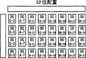
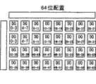
图6示出了存储单元阵列的位分配,其中图6a示出了4位配置,图6b示出了8位配置,图6c示出了16位配置,图6d示出了32位配置,图6e示出了64位配置,以及图6f示出了128位配置;Figure 6 shows the bit allocation of the memory cell array, where Figure 6a shows a 4-bit configuration, Figure 6b shows an 8-bit configuration, Figure 6c shows a 16-bit configuration, and Figure 6d shows a 32-bit configuration, Fig. 6e shows a 64-bit configuration, and Figure 6f shows a 128-bit configuration;
图7示出了存储器配置切换电路的概念图;7 shows a conceptual diagram of a memory configuration switching circuit;
图8示出了位切换电路的配置;Fig. 8 shows the configuration of the bit switching circuit;
图9示出了通过切换操作实现的接线的重排列,其中图9a示出了4位配置,图9b示出了8位配置,图9c示出了16位配置,图9d示出了32位配置;Figure 9 shows the rearrangement of wiring achieved by switching operations, where Figure 9a shows a 4-bit configuration, Figure 9b shows an 8-bit configuration, Figure 9c shows a 16-bit configuration, and Figure 9d shows a 32-bit configuration configuration;
图10是存储单元阵列芯片的存储体的分配的概念图;Fig. 10 is a conceptual diagram of allocation of memory banks of a memory cell array chip;
图11示出了与512Mb的DRAM的多个位及多个存储体相对应的字数;Fig. 11 shows the number of words corresponding to a plurality of bits and a plurality of storage banks of a DRAM of 512Mb;
图12示出了用于切换数据传输速率的电路的配置;以及Fig. 12 shows the configuration of the circuit for switching the data transmission rate; and
图13示出了在切换数据传输速率时被用作锁存器输入的时钟波形。Figure 13 shows the clock waveforms used as the latch input when switching the data transfer rate.
具体实施方式Detailed ways
接下来,将参考附图解释本发明的工作示例。Next, working examples of the present invention will be explained with reference to the drawings.
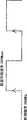
图1是根据本发明的堆叠式存储器器件的工作示例的配置的示意图。FIG. 1 is a schematic diagram of a configuration of a working example of a stacked memory device according to the present invention.
如图1所示,本工作示例由如下部分组成:存储单元阵列芯片101、存储器单元102、输入/输出缓冲器103、地址缓冲器104、接口芯片105、芯片间接线106、存储器配置切换电路107、地址缓冲器108、行译码器109、列译码器110和存储单元阵列111。As shown in Figure 1, this working example is composed of the following parts: memory
存储单元阵列由排列成矩阵形式的多个存储器单元102组成;该矩阵与行译码器109和列译码器110集成在一起,以组成存储单元阵列芯片101。接口芯片105由地址缓冲器104、输入/输出缓冲器103和存储器配置切换电路107组成;并且与存储单元阵列芯片101堆叠在一起;并通过芯片间接线106连接到存储单元阵列芯片101。The memory cell array is composed of a plurality of
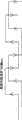
存储单元阵列芯片101的存储单元阵列111与接口芯片105的存储器配置切换电路107利用堆叠式结构的优点,通过j×k条芯片间接线106连接在一起,以实现高度并行的数据传输。由于堆叠式配置,芯片面积小于具有现有平面配置的相同容量存储器器件。另外,如图2所示,将多个存储单元阵列芯片101堆叠起来允许了面积效率的进一步增加。The
接下来,将解释用于切换存储器器件的输入/输出位配置的装置。存储单元阵列111由n个存储器单元102组成。存储单元阵列111通过四位(DQ0、DQ1、DQ2、DQ3)的数据总线连接到存储器配置切换电路107,其中四位数据总线是由来自每个存储器单元102的四条芯片间接线106组成的,因此数据总线的总位数是4n。Next, means for switching the input/output bit configuration of the memory device will be explained. The
如图3a所示,如果来自所有n个存储器单元的数据总线通过存储器配置切换电路107根据DQ被组织在一起,则输入/输出位数是4。如图3b所示,在n/2个存储器单元中排列数据总线,则得到八个输入/输出位;如图3c所示,在n/4个存储器单元中排列数据总线,则得到16个输入/输出位;并且如果来自n个存储器单元的数据总线被并行连接到输入/输出缓冲器而不进行改变,则实现了4n位的输入/输出配置,如图3d所示。As shown in FIG. 3a, if the data buses from all n memory cells are organized together according to DQ through the memory
如前述解释中所述,通过使用接口芯片105上的存储器配置切换电路107来切换芯片之间的大并行数目的数据总线接线,使得存储器器件的输入/输出位配置能够在一个存储单元阵列芯片101上从4位到4n位的大范围上切换。As described in the foregoing explanation, by using the memory
另外,通过在接口芯片105中的存储器配置切换电路107的数据总线上提供锁存器,预取数据,然后控制锁存器的时钟定时,实现了外部接口的双倍或四倍数据传输速率,而不用改变存储单元阵列111的时钟频率。In addition, by providing a latch on the data bus of the memory
接下来,将参考附图解释本发明的工作示例的细节。Next, details of working examples of the present invention will be explained with reference to the drawings.
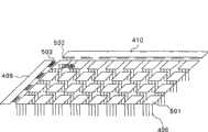
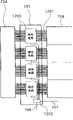
图4示出了根据本发明的512Mb堆叠式DRAM器件的工作示例的配置。在图4中,存储单元阵列芯片401、存储器单元、输入/输出缓冲器、地址缓冲器404、接口芯片405、芯片间接线406、存储器配置切换电路407、地址缓冲器408、行译码器409、列译码器410和存储单元阵列411中的每一个都分别等同于图1所示的存储单元阵列芯片101、存储器单元102、输入/输出缓冲器103、地址缓冲器104、接口芯片105、芯片间接线106、存储器配置切换电路107、地址缓冲器108、行译码器109、列译码器110和存储单元阵列111。FIG. 4 shows the configuration of a working example of a 512Mb stacked DRAM device according to the present invention. In FIG. 4, memory
存储单元阵列芯片401堆叠在接口芯片405上。存储单元阵列芯片401具有四存储体配置(BL0、BK1、BK2、BK3),每个存储体具有128Mb存储单元阵列411、行译码器409和列译码器410。接口芯片405具有存储器配置切换电路407、地址缓冲器404和输入/输出缓冲器。存储单元阵列芯片401的存储单元阵列与接口芯片405的存储器配置切换电路407通过数据总线连接在一起,并且行译码器409和列译码器410通过地址总线连接到地址缓冲器404。这些总线中每一个都应用芯片间接线406,芯片间接线406是贯穿式(through-type)接线,它们具有穿过芯片的100μm或更短的极短距离;并且这些数据总线由于它们大约为20μm量级的大直径以及低电阻,实现了GHz数量级的高速传输。The memory
图5示出了存储单元阵列411的详细视图,其中图5a示出了存储体部分的细节,以及图5b示出了内部配置。128Mb存储单元阵列411由32个4Mb存储器单元501组成。从每个4Mb存储器单元501延伸出四条芯片间接线406,这些芯片间接线406组成4位数据总线。4Mb存储器单元501具有4位1兆字配置,并且如图5b(关于4Mb存储器单元501的内部配置)所示,来自列译码器410的1024条数据选择线502和来自行译码器409的1024条字线503与存储器单元连接在一起,并且在数据选择线502和字线503的交叉点处的四个DQ部分DQ0、DQ1、DQ2和DQ3处具有存储单元505。Fig. 5 shows a detailed view of the
在读取数据时,由每个存储单元505的数据决定的数据线的小振幅差分信号被读出放大器504和数据放大器507转换为全振幅信号,并且被发送到四位(DQ0、DQ1、DQ2和DQ3)数据总线。在写入时,从四位数据总线将数据发送到已经在数据选择线502处被选中的四条数据线,并且数据被写入与所选中的字线503的交叉点处的四个DQ部分的存储单元505。四位数据总线通过四条芯片间接线与接口芯片405交换数据。When reading data, the small-amplitude differential signal of the data line determined by the data of each
图6示出了在改变存储体内的输入/输出位配置时存储单元阵列411的DQ位分配。通过利用接口芯片405的存储器配置切换电路407来改变从存储单元阵列芯片401的一个存储体连接出来的128条数据总线接线的组合方式,改变了输入/输出位数。通过使用具有四个DQ的4Mb存储器单元作为最小单元,可以如图6a~6f那样分配×4、×8、×32、×64以及×128的位配置。FIG. 6 shows the DQ bit allocation of the
图7是示出了存储器接口芯片405的存储器配置切换电路702的配置的框图。存储器配置切换电路702由位切换电路708、预取切换电路701和切换控制电路706组成。位切换电路708重新排列来自存储单元阵列芯片401的数据总线接线。FIG. 7 is a block diagram showing the configuration of the memory
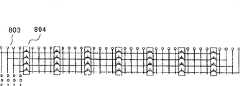
图8是示出了位切换电路708的详细配置的框图。从图4和图5a所示的存储单元阵列芯片401中的4Mb存储器单元501延伸出来的四条芯片间接线406连接到图8所示的位切换电路708的四位配线单元803,并且与存储器单元一样,这些位切换电路708被配置在八个水平行和四个竖直列中,总共32个。每个配线单元803之间的连接是通过由四个晶体管的传输门组成的四开关阵列801和804实现的。另外,来自位切换电路708的接线经由预取切换电路701连接到输入/输出缓冲器412。FIG. 8 is a block diagram showing a detailed configuration of the
图9示出了其中八个4位配线单元803被水平排列在位切换电路708内的部分,其中通过在4位配线单元803之间切换4开关阵列804来切换位数。FIG. 9 shows a portion in which eight 4-
接通图9中被方框包围的4开关阵列804能够设置图9a~9d中所示的×4、×8、×16和×32的位配置。通过将图9d所示的32位配置进一步在竖直方向连接至四行,并且然后切换放置于其间的开关阵列,使得能够设置与图6d~6f相对应的×32、×64、和×128的输入/输出位配置。Turning on the 4-
位切换电路708的切换控制信号是从切换控制电路706发送的。作为切换控制电路的一种配置,可以建议这样的配置:在切换控制电路706的接线中提供熔丝,该电路被配置为在芯片制造之后通过根据存储器配置的规格切断这些熔丝,来提供实现所希望的存储器配置的开关的控制信号。作为该配置的一种替代,也可以提出这样的配置:切换控制电路706是根据焊接选项输入信号的组合进行操作的逻辑电路,该逻辑电路被配置为在封装芯片时通过根据所希望的输入/输出位配置规格将焊接选项焊盘和封装管脚之间焊接起来,来输出实现所希望的存储器配置的开关的控制信号。The switching control signal of the
虽然在本工作示例中只示出了一个存储单元阵列芯片,但是通过采用其中多个芯片被堆叠在一起的形式,使得能够根据芯片数目增加存储器器件的存储容量,并且允许相似的存储器配置切换。另外,虽然在本工作示例中使用DRAM作为存储器器件,但是类似的配置也可以使用SRAM。Although only one memory cell array chip is shown in this working example, adopting a form in which a plurality of chips are stacked enables the storage capacity of the memory device to be increased according to the number of chips and allows similar switching of memory configurations. Also, although DRAM is used as the memory device in this working example, a similar configuration can also use SRAM.
存储单元阵列芯片允许如图10所示那样将存储体数目更改为一个存储体、两个存储体或四个存储体,并且当存储单元阵列芯片的存储容量是512Mb时,取决于图11所示的存储体数目和输入/输出位数,可以有21种存储器配置。当采用具有多个存储体的配置时,可以在存储体单元中指定地址,然后对存储单元进行存取,由此,当对特定存储体中的存储单元进行存取时,可以在其他存储体中执行交错操作(诸如预充电),或者,还可以执行用于选择字线以及激活位线的操作,以及刷新操作。结果,可以相继对存储体进行存取,而无需中断,并且传输了数据。The memory cell array chip allows the number of memory banks to be changed to one memory bank, two memory banks, or four memory banks as shown in Figure 10, and when the memory capacity of the memory cell array chip is 512Mb, it depends on the number of banks shown in Figure 11 The number of memory banks and the number of input/output bits can have 21 memory configurations. When a configuration with multiple banks is employed, it is possible to specify addresses in bank units and then access the memory units, whereby when accessing a memory unit in a specific bank, it is possible to access memory units in other banks. An interleave operation such as precharge is performed, or an operation for selecting a word line and activating a bit line, and a refresh operation may also be performed. As a result, memory banks can be accessed successively without interruption, and data is transferred.
接下来,将解释一种无需改变存储器核心的工作频率就能切换时钟定时以及预取切换电路701中的预取数目并改变存储器器件和外部之间的数据传输速率的装置。Next, a means for switching the clock timing and the number of prefetches in the
在图12中,来自位切换电路708的数据经由四组32位数据总线1201被发送到预取切换电路701。预取切换701具有与四组32位数据总线中每一个相对应的四个锁存电路1203、与时钟线705和控制信号线707连接的时钟控制电路1202;预取切换电路701根据经由控制信号线707发送来的控制信号来调节经由时钟线705发送来的时钟信号;并且将这些时钟信号提供给每个锁存电路1203,作为每个锁存电路1203锁存数据所依据的定时信号。In FIG. 12 , data from
控制在预取切换电路701中锁存数据的定时,所锁存的数据被发送到输入/输出缓冲器704,并且将向外部的传输速率切换至双倍或四倍原始速率。The timing of latching data in the
如图13a所示,当频率是与存储单元阵列芯片401的时钟频率相同的200MHz的时钟作为锁存器的输入并且四组32位数据总线1201的所有数据在时钟的上升时刻被发送到输入/输出缓冲器704时,输入/输出数据传输速率达到128输入/输出位处的200Mbps。当四组32位数据总线1201中的两组在时钟上升时刻被锁存且其他两组在时钟下降时刻被锁存时,数据传输速率被加倍到64输入/输出位的400Mbps(图13b)。如图13c所示,当应用于锁存器的时钟进一步被设置为相移了π/2的两个相位,并且时钟信的上升时刻和下降时刻都被用来实现四组32位数据总线在800MHz周期的定时处的锁存时,数据传输速率达到32输入/输出位、800Mbps。用于切换每个锁存电路1203的输入时钟的控制信号是从切换控制电路发送的,与用于切换输入/输出位配置的控制信号一样。这样,通过将预取数目改变为1、2和4,使得不仅能够切换输入/输出位配置,还能切换数据传输速率。As shown in Figure 13a, when the frequency is the same 200MHz clock as the clock frequency of the memory
Claims (6)
Translated fromChineseApplications Claiming Priority (2)
| Application Number | Priority Date | Filing Date | Title |
|---|---|---|---|
| JP2004190317 | 2004-06-28 | ||
| JP2004190317AJP4662740B2 (en) | 2004-06-28 | 2004-06-28 | Stacked semiconductor memory device |
Publications (2)
| Publication Number | Publication Date |
|---|---|
| CN1725366A CN1725366A (en) | 2006-01-25 |
| CN100543864Ctrue CN100543864C (en) | 2009-09-23 |
Family
ID=35504701
Family Applications (1)
| Application Number | Title | Priority Date | Filing Date |
|---|---|---|---|
| CNB2005100810298AExpired - Fee RelatedCN100543864C (en) | 2004-06-28 | 2005-06-28 | Stacked semiconductor memory device |
Country Status (4)
| Country | Link |
|---|---|
| US (1) | US7221614B2 (en) |
| JP (1) | JP4662740B2 (en) |
| CN (1) | CN100543864C (en) |
| TW (1) | TWI291226B (en) |
Families Citing this family (55)
| Publication number | Priority date | Publication date | Assignee | Title |
|---|---|---|---|---|
| US8244971B2 (en) | 2006-07-31 | 2012-08-14 | Google Inc. | Memory circuit system and method |
| US10013371B2 (en) | 2005-06-24 | 2018-07-03 | Google Llc | Configurable memory circuit system and method |
| US8041881B2 (en) | 2006-07-31 | 2011-10-18 | Google Inc. | Memory device with emulated characteristics |
| US8089795B2 (en) | 2006-02-09 | 2012-01-03 | Google Inc. | Memory module with memory stack and interface with enhanced capabilities |
| US20080082763A1 (en) | 2006-10-02 | 2008-04-03 | Metaram, Inc. | Apparatus and method for power management of memory circuits by a system or component thereof |
| US7590796B2 (en) | 2006-07-31 | 2009-09-15 | Metaram, Inc. | System and method for power management in memory systems |
| US8060774B2 (en) | 2005-06-24 | 2011-11-15 | Google Inc. | Memory systems and memory modules |
| US8335894B1 (en) | 2008-07-25 | 2012-12-18 | Google Inc. | Configurable memory system with interface circuit |
| US8081474B1 (en) | 2007-12-18 | 2011-12-20 | Google Inc. | Embossed heat spreader |
| US7609567B2 (en) | 2005-06-24 | 2009-10-27 | Metaram, Inc. | System and method for simulating an aspect of a memory circuit |
| US8055833B2 (en) | 2006-10-05 | 2011-11-08 | Google Inc. | System and method for increasing capacity, performance, and flexibility of flash storage |
| KR101377305B1 (en) | 2005-06-24 | 2014-03-25 | 구글 인코포레이티드 | An integrated memory core and memory interface circuit |
| US8438328B2 (en) | 2008-02-21 | 2013-05-07 | Google Inc. | Emulation of abstracted DIMMs using abstracted DRAMs |
| US8386722B1 (en) | 2008-06-23 | 2013-02-26 | Google Inc. | Stacked DIMM memory interface |
| US9171585B2 (en) | 2005-06-24 | 2015-10-27 | Google Inc. | Configurable memory circuit system and method |
| US8130560B1 (en) | 2006-11-13 | 2012-03-06 | Google Inc. | Multi-rank partial width memory modules |
| US8111566B1 (en) | 2007-11-16 | 2012-02-07 | Google, Inc. | Optimal channel design for memory devices for providing a high-speed memory interface |
| US7580312B2 (en)* | 2006-07-31 | 2009-08-25 | Metaram, Inc. | Power saving system and method for use with a plurality of memory circuits |
| US8090897B2 (en) | 2006-07-31 | 2012-01-03 | Google Inc. | System and method for simulating an aspect of a memory circuit |
| US8077535B2 (en) | 2006-07-31 | 2011-12-13 | Google Inc. | Memory refresh apparatus and method |
| US7392338B2 (en) | 2006-07-31 | 2008-06-24 | Metaram, Inc. | Interface circuit system and method for autonomously performing power management operations in conjunction with a plurality of memory circuits |
| US9507739B2 (en) | 2005-06-24 | 2016-11-29 | Google Inc. | Configurable memory circuit system and method |
| US8359187B2 (en) | 2005-06-24 | 2013-01-22 | Google Inc. | Simulating a different number of memory circuit devices |
| US20080028136A1 (en) | 2006-07-31 | 2008-01-31 | Schakel Keith R | Method and apparatus for refresh management of memory modules |
| US8796830B1 (en) | 2006-09-01 | 2014-08-05 | Google Inc. | Stackable low-profile lead frame package |
| US7386656B2 (en) | 2006-07-31 | 2008-06-10 | Metaram, Inc. | Interface circuit system and method for performing power management operations in conjunction with only a portion of a memory circuit |
| US8327104B2 (en) | 2006-07-31 | 2012-12-04 | Google Inc. | Adjusting the timing of signals associated with a memory system |
| US8397013B1 (en) | 2006-10-05 | 2013-03-12 | Google Inc. | Hybrid memory module |
| US9542352B2 (en) | 2006-02-09 | 2017-01-10 | Google Inc. | System and method for reducing command scheduling constraints of memory circuits |
| US7827345B2 (en)* | 2005-08-04 | 2010-11-02 | Joel Henry Hinrichs | Serially interfaced random access memory |
| JP5098644B2 (en)* | 2005-08-23 | 2012-12-12 | 日本電気株式会社 | Semiconductor device and semiconductor chip |
| WO2007028109A2 (en) | 2005-09-02 | 2007-03-08 | Metaram, Inc. | Methods and apparatus of stacking drams |
| JP2007200963A (en)* | 2006-01-24 | 2007-08-09 | Hitachi Ltd | Semiconductor memory device |
| US9632929B2 (en) | 2006-02-09 | 2017-04-25 | Google Inc. | Translating an address associated with a command communicated between a system and memory circuits |
| KR100809689B1 (en) | 2006-06-16 | 2008-03-06 | 삼성전자주식회사 | Semiconductor device for mounting interface chip embedded with substrate through-electrode |
| US7724589B2 (en) | 2006-07-31 | 2010-05-25 | Google Inc. | System and method for delaying a signal communicated from a system to at least one of a plurality of memory circuits |
| JP4364226B2 (en)* | 2006-09-21 | 2009-11-11 | 株式会社東芝 | Semiconductor integrated circuit |
| JP4245180B2 (en) | 2006-10-30 | 2009-03-25 | エルピーダメモリ株式会社 | Stacked memory |
| JP5616636B2 (en) | 2006-12-14 | 2014-10-29 | ラムバス・インコーポレーテッド | Multi-die memory device |
| WO2008079910A2 (en) | 2006-12-20 | 2008-07-03 | Rambus Inc. | Strobe acquisition and tracking |
| US8209479B2 (en) | 2007-07-18 | 2012-06-26 | Google Inc. | Memory circuit system and method |
| US8080874B1 (en) | 2007-09-14 | 2011-12-20 | Google Inc. | Providing additional space between an integrated circuit and a circuit board for positioning a component therebetween |
| KR101448150B1 (en) | 2007-10-04 | 2014-10-08 | 삼성전자주식회사 | A multi-chip package memory in which memory chips are stacked, a method of stacking memory chips, and a method of controlling operations of a multi-chip package memory |
| KR101519061B1 (en) | 2008-01-21 | 2015-05-11 | 삼성전자주식회사 | Flash memory device having row decoder sharing single high voltage level shift |
| KR101393311B1 (en) | 2008-03-19 | 2014-05-12 | 삼성전자주식회사 | Multi-chip package memory for compensating process variation |
| JP5632584B2 (en)* | 2009-02-05 | 2014-11-26 | ピーエスフォー ルクスコ エスエイアールエルPS4 Luxco S.a.r.l. | Semiconductor device |
| DE202010017690U1 (en) | 2009-06-09 | 2012-05-29 | Google, Inc. | Programming dimming terminating resistor values |
| WO2011093863A1 (en) | 2010-01-29 | 2011-08-04 | Hewlett-Packard Development Company, L.P. | Three dimensional multilayer circuit |
| US7982504B1 (en) | 2010-01-29 | 2011-07-19 | Hewlett Packard Development Company, L.P. | Interconnection architecture for multilayer circuits |
| TW201207852A (en)* | 2010-04-05 | 2012-02-16 | Mosaid Technologies Inc | Semiconductor memory device having a three-dimensional structure |
| US8854865B2 (en)* | 2010-11-24 | 2014-10-07 | Semiconductor Energy Laboratory Co., Ltd. | Semiconductor memory device |
| US9558791B2 (en)* | 2013-12-05 | 2017-01-31 | Taiwan Semiconductor Manufacturing Company Limited | Three-dimensional static random access memory device structures |
| JP7102119B2 (en) | 2017-09-29 | 2022-07-19 | キヤノン株式会社 | Semiconductor devices and equipment |
| US11004477B2 (en)* | 2018-07-31 | 2021-05-11 | Micron Technology, Inc. | Bank and channel structure of stacked semiconductor device |
| CN115151972A (en)* | 2020-02-28 | 2022-10-04 | 华为技术有限公司 | Memory and electronic equipment |
Family Cites Families (17)
| Publication number | Priority date | Publication date | Assignee | Title |
|---|---|---|---|---|
| US4398248A (en)* | 1980-10-20 | 1983-08-09 | Mcdonnell Douglas Corporation | Adaptive WSI/MNOS solid state memory system |
| JPH02116084A (en)* | 1988-10-25 | 1990-04-27 | Nec Corp | Semiconductor memory |
| JPH04196263A (en) | 1990-11-27 | 1992-07-16 | Mitsubishi Electric Corp | semiconductor integrated circuit |
| JP2605968B2 (en)* | 1993-04-06 | 1997-04-30 | 日本電気株式会社 | Semiconductor integrated circuit and method of forming the same |
| JPH09223389A (en)* | 1996-02-15 | 1997-08-26 | Mitsubishi Electric Corp | Synchronous semiconductor memory device |
| KR100278653B1 (en)* | 1998-01-23 | 2001-02-01 | 윤종용 | Double data rate semiconductor memory device |
| JP2001035152A (en) | 1999-07-22 | 2001-02-09 | Hitachi Ltd | Semiconductor storage device |
| JP2002026283A (en) | 2000-06-30 | 2002-01-25 | Seiko Epson Corp | Multi-layered memory device and method of manufacturing the same |
| JP2002025250A (en)* | 2000-07-03 | 2002-01-25 | Hitachi Ltd | Semiconductor storage device |
| US6487102B1 (en)* | 2000-09-18 | 2002-11-26 | Intel Corporation | Memory module having buffer for isolating stacked memory devices |
| JP2002251884A (en)* | 2001-02-21 | 2002-09-06 | Toshiba Corp | Semiconductor memory device and system device thereof |
| JP3872320B2 (en)* | 2001-08-22 | 2007-01-24 | 松下電器産業株式会社 | Semiconductor memory device and bonding method thereof |
| US6504742B1 (en) | 2001-10-31 | 2003-01-07 | Hewlett-Packard Company | 3-D memory device for large storage capacity |
| JP2003204030A (en) | 2002-01-07 | 2003-07-18 | Hitachi Ltd | Semiconductor device and method of manufacturing the same |
| JP2003338200A (en)* | 2002-05-17 | 2003-11-28 | Mitsubishi Electric Corp | Semiconductor integrated circuit device |
| JP4499982B2 (en) | 2002-09-11 | 2010-07-14 | 株式会社日立製作所 | Memory system |
| JP4045506B2 (en)* | 2004-01-21 | 2008-02-13 | セイコーエプソン株式会社 | Stacked semiconductor memory device |
- 2004
- 2004-06-28JPJP2004190317Apatent/JP4662740B2/ennot_activeExpired - Lifetime
- 2005
- 2005-06-14USUS11/151,220patent/US7221614B2/ennot_activeExpired - Lifetime
- 2005-06-24TWTW094121194Apatent/TWI291226B/ennot_activeIP Right Cessation
- 2005-06-28CNCNB2005100810298Apatent/CN100543864C/ennot_activeExpired - Fee Related
Also Published As
| Publication number | Publication date |
|---|---|
| TWI291226B (en) | 2007-12-11 |
| TW200620633A (en) | 2006-06-16 |
| CN1725366A (en) | 2006-01-25 |
| JP2006012337A (en) | 2006-01-12 |
| JP4662740B2 (en) | 2011-03-30 |
| US7221614B2 (en) | 2007-05-22 |
| US20050285174A1 (en) | 2005-12-29 |
Similar Documents
| Publication | Publication Date | Title |
|---|---|---|
| CN100543864C (en) | Stacked semiconductor memory device | |
| CN100383968C (en) | Stacked semiconductor memory device | |
| KR101318116B1 (en) | An integrated memory core and memory interface circuit | |
| US7830692B2 (en) | Multi-chip memory device with stacked memory chips, method of stacking memory chips, and method of controlling operation of multi-chip package memory | |
| JP4421957B2 (en) | 3D semiconductor device | |
| US7558096B2 (en) | Stacked memory | |
| US6877071B2 (en) | Multi-ported memory | |
| JPH1050958A (en) | Semiconductor storage device, layout method of semiconductor storage device, operation method of semiconductor storage device, and circuit arrangement pattern of semiconductor storage device | |
| JP2004500673A5 (en) | ||
| US20130227229A1 (en) | Semiconductor device that burst-outputs read data | |
| JP2012155814A (en) | Semiconductor device and information processing system including the same | |
| JP5599969B2 (en) | Multi-port memory and computer system including the multi-port memory | |
| US9361973B2 (en) | Multi-channel, multi-bank memory with wide data input/output | |
| KR20220169140A (en) | Memory device and semiconductor device including the same | |
| WO2010001833A1 (en) | Memory/logic conjugate system | |
| US8355270B2 (en) | Semiconductor device having open bit line architecture | |
| JP2013020678A (en) | Semiconductor memory device | |
| US6791896B2 (en) | Semiconductor memory device capable of changing an address space thereof | |
| JPH02246149A (en) | Semiconductor integrated circuit device and method for remedying defect thereof | |
| JPH08255479A (en) | Semiconductor memory device | |
| US6914796B1 (en) | Semiconductor memory element with direct connection of the I/Os to the array logic | |
| US20080098152A1 (en) | Method and apparatus for configuring a memory device | |
| JP2000058772A (en) | Semiconductor memory device | |
| KR20010002116A (en) | Semiconductor integrated circuit using SRAM between DRAM and logic circuit as buffer | |
| US6882590B2 (en) | Multiple configuration multiple chip memory device and method |
Legal Events
| Date | Code | Title | Description |
|---|---|---|---|
| C06 | Publication | ||
| PB01 | Publication | ||
| C10 | Entry into substantive examination | ||
| SE01 | Entry into force of request for substantive examination | ||
| C14 | Grant of patent or utility model | ||
| GR01 | Patent grant | ||
| C17 | Cessation of patent right | ||
| CF01 | Termination of patent right due to non-payment of annual fee | Granted publication date:20090923 Termination date:20120628 |