CN100541465C - Device and integrated circuit for generating a plurality of different gate pulse signals - Google Patents
Device and integrated circuit for generating a plurality of different gate pulse signalsDownload PDFInfo
- Publication number
- CN100541465C CN100541465CCN200480044264.1ACN200480044264ACN100541465CCN 100541465 CCN100541465 CCN 100541465CCN 200480044264 ACN200480044264 ACN 200480044264ACN 100541465 CCN100541465 CCN 100541465C
- Authority
- CN
- China
- Prior art keywords
- strobe
- strobe signal
- pulse
- multiplexed
- different
- Prior art date
- Legal status (The legal status is an assumption and is not a legal conclusion. Google has not performed a legal analysis and makes no representation as to the accuracy of the status listed.)
- Expired - Fee Related
Links
Images


Classifications
- G—PHYSICS
- G06—COMPUTING OR CALCULATING; COUNTING
- G06F—ELECTRIC DIGITAL DATA PROCESSING
- G06F13/00—Interconnection of, or transfer of information or other signals between, memories, input/output devices or central processing units
- G06F13/38—Information transfer, e.g. on bus
- G06F13/42—Bus transfer protocol, e.g. handshake; Synchronisation
- G06F13/4282—Bus transfer protocol, e.g. handshake; Synchronisation on a serial bus, e.g. I2C bus, SPI bus
- G06F13/4291—Bus transfer protocol, e.g. handshake; Synchronisation on a serial bus, e.g. I2C bus, SPI bus using a clocked protocol
Landscapes
- Engineering & Computer Science (AREA)
- Theoretical Computer Science (AREA)
- Physics & Mathematics (AREA)
- General Engineering & Computer Science (AREA)
- General Physics & Mathematics (AREA)
- Mobile Radio Communication Systems (AREA)
- Transceivers (AREA)
Abstract
Description
Translated fromChinese技术领域technical field
本发明涉及一种装置及其控制接口。本发明可适用于,但不限于无线通信设备的控制接口,特别是多模无线通信设备的控制接口。The invention relates to a device and its control interface. The present invention is applicable to, but not limited to, the control interface of wireless communication equipment, especially the control interface of multi-mode wireless communication equipment.
背景技术Background technique
诸如移动电话那样的无线通信设备需要非常高的硬件和固件/软件的集成度以便获得必要的功能性密度,也就是在最小设备体积内以最小成本实现必要的功能性。一种最佳的无线通信设备设计也必须最小化功率消耗以便增加电池通话时间和/或待机时间。Wireless communication devices such as mobile phones require a very high level of integration of hardware and firmware/software in order to achieve the necessary functional density, ie to achieve the necessary functionality in the smallest device volume and at the lowest cost. An optimal wireless communication device design must also minimize power consumption in order to increase battery talk time and/or standby time.
无线通信设备还包含多个截然不同并且可操作地耦合的子系统,以便提供复合无线通信设备需要执行的多种功能和操作。所述子系统包括:射频功率放大功能;射频集成电路(RFIC),包括射频生成、放大、滤波等等功能;基带集成电路(BBIC),包括音频电路、编码/解码、(解)调制功能、和处理功能等等;以及存储单元。A wireless communication device also includes a number of distinct and operably coupled subsystems in order to provide the various functions and operations that a composite wireless communication device is required to perform. The subsystem includes: radio frequency power amplification function; radio frequency integrated circuit (RFIC), including functions such as radio frequency generation, amplification, filtering, etc.; baseband integrated circuit (BBIC), including audio circuit, encoding/decoding, (de)modulation function, and processing functions, etc.; and storage units.
通常将接口标准化以在各个子系统之间进行通信,所述接口通常被标准化以使得不同的芯片组制造商和不同的手机制造商之间具有通用性和增强的功能性。Interfaces are typically standardized to communicate between the various subsystems, which are typically standardized to allow commonality and enhanced functionality between different chipset manufacturers and different handset manufacturers.
在无线通信设备中存在的一个典型的接口是基带集成电路(BBIC)和射频集成电路(RFIC)之间的接口。IC上的接触引脚(contactpin)用于在设备/元件/功能之间发送电信号。通常期望将无线通信设备中所使用的IC中的引脚的数量最小化,但是由于例如在BBIC-RFIC接口上使用了额外引脚,则增加了IC面积,也增加了IC成本和复杂度并且还增加了功率消耗。A typical interface that exists in a wireless communication device is an interface between a baseband integrated circuit (BBIC) and a radio frequency integrated circuit (RFIC). Contact pins on ICs are used to send electrical signals between devices/components/functions. It is generally desirable to minimize the number of pins in ICs used in wireless communication devices, but due to the use of extra pins, for example on the BBIC-RFIC interface, IC area is increased, IC cost and complexity are also increased and Power consumption is also increased.
在移动电话领域中,组建了移动电话制造商协会来定义各种子系统接口,所述子系统接口特别是指当转移以覆盖另外的、未来的无线通信技术(诸如另外使用第三代(3G)宽带码分多址(WCDMA)技术的多模式收发器)时、在各种不同的第二代蜂窝式式电话(2.xG)的变化之间的接口。该协会被称为‘DigRF’,并且能够在其网站www.digrf.com上找到所定义接口及其功能性的细节,特别是多模式移动电话方案下的细节。多模式操作规范目前尚未应用。In the field of mobile telephony, the Association of Mobile Telephone Manufacturers has been formed to define various subsystem interfaces, especially when migrating to cover additional, future wireless communication technologies such as the additional use of third generation (3G ) wideband code division multiple access (WCDMA) technology multimode transceiver) interface between various second generation cellular telephone (2.xG) variations. The consortium is called 'DigRF' and details of the defined interfaces and their functionality can be found on its websitewww.digrf.com , in particular under the multimode mobile phone scheme. The multi-mode operation specification is not currently applied.
由DigRF协会进行标准化的一个接口是BB-RF接口,其包括用于接收(Rx)和发送(Tx)第二代便携式电话(2.xG)芯片组的的变化的一系列数据/控制接口。当定义接口以适应3G技术所需的增加的复杂度和数据率时,很明显地,将IC引脚数量最小化将十分有利。One interface standardized by the DigRF Association is the BB-RF interface, which includes a series of data/control interfaces for receiving (Rx) and transmitting (Tx) a variation of second generation cellular phone (2.xG) chipsets. When defining interfaces to accommodate the increased complexity and data rates required by 3G technologies, it is clear that minimizing the IC pin count will be beneficial.
2.xG标准包含用于例如在RFIC和BBIC之间传送层1定时信息的选通脉冲信号(strobe signal)。注意,选通脉冲信号的宽度和幅度是固定的。所以,所有的选通脉冲彼此之间是无法区分的。此外,利用2.xG收发器(TRX)的接口标准的开发还仅是在想象阶段。在BBICRFIC接口上,提供选通脉冲信号以在RFIC内支持精确的事件定时。2. The xG standard includes a strobe signal for conveying
然而,可以预见将来的无线通信设备需要适应多路通信模式。迄今为止,还没有提出使用同一接口以将层1定时信息传送到多路接收器的解决方案。本发明的发明人认识并意识到:复制引脚(诸如用于支持选通脉冲信号的2.xG IC引脚)以适应多模式的的这种显见方案是对宝贵资源的浪费。However, it is foreseeable that future wireless communication devices will need to accommodate multiple communication modes. So far, no solution has been proposed to use the same interface to communicate
IBM的美国专利申请US 2004/30071015A1公开了在SDRAM(存储器)接口领域中使用选通脉冲信号。选择“单个”选通脉冲信号以精确地将数据锁存到同步动态随机存取存储器(SDRAM)。还描述了从不同的源发送单个选通脉冲信号的原理。IBM's US patent application US 2004/30071015A1 discloses the use of strobe signals in the field of SDRAM (memory) interfaces. Select the "single" strobe signal to accurately latch data into Synchronous Dynamic Random Access Memory (SDRAM). The principle of sending a single strobe signal from different sources is also described.
然而,因为US 2004/30071015A1提出为每一功能锁存单个选通脉冲信号,所以其提出的技术仍旧不能解决上述浪费宝贵资源的问题。However, since US 2004/30071015A1 proposes to latch a single strobe signal for each function, the proposed technique still cannot solve the above-mentioned problem of wasting precious resources.
发明人为Kuge等且申请人为Renesas Technology Corporation的美国专利US 6,715,096B2描述了另一对存储器IC的接口使用选通脉冲信号的技术。US 6,715,096B2公开了一种用于以最佳的选通脉冲定时执行数据采样的接口电路设备,其通过使用所存储的数据窗口信息以确定选通脉冲定时。US 6,715,096B2强调了一种接口,其中通过为写/读(W/R)存储器而选择有关锁存选通脉冲的最佳延迟以正确地将数据锁存到存储器。US Patent No. 6,715,096B2, the inventor of which is Kuge et al. and the applicant is Renesas Technology Corporation, describes another technique of using a strobe signal for the interface of a memory IC. US 6,715,096 B2 discloses an interface circuit device for performing data sampling with optimal strobe timing by using stored data window information to determine the strobe timing. US 6,715,096B2 emphasizes an interface in which data is correctly latched to the memory by choosing the optimum delay with respect to the latch strobe for writing/reading (W/R) the memory.
所以,例如在无线通信设备中,需要这样一种机制,其包含了集成电路/子系统和相应的控制接口,所述集成电路/子系统和相应的控制接口在不增加成本或复杂度或增加引脚数量的情况下支持多路设备(例如收发器)的选通脉冲信号。So, for example, in wireless communication devices, there is a need for a mechanism that incorporates an integrated circuit/subsystem and corresponding control interface without adding cost or complexity or adding Supports strobe signals for multiplexed devices (such as transceivers) without the number of pins.
发明内容Contents of the invention
本发明的目的在于解决上述问题。The object of the present invention is to solve the above-mentioned problems.
为了解决上述一个或多个技术问题,根据本发明的第一方面,提供一种装置,包括:操作耦合在基带子系统和射频子系统之间以在其之间传送数据的控制接口,以及操作耦合到控制接口的选通脉冲生成功能部件,其中所述装置的特征在于:构造所述选通脉冲生成功能部件以基于对多路选通脉冲的电压幅度特性的区分和/或对多路选通脉冲的脉冲宽度的区分或对多路选通脉冲所使用的代码的区分而生成在不同的预期接收设备之间有所区别的多个不同的选通脉冲信号。In order to solve one or more technical problems above, according to a first aspect of the present invention, an apparatus is provided, including: a control interface operatively coupled between a baseband subsystem and a radio frequency subsystem to transmit data therebetween, and an operation A strobe generation function coupled to the control interface, wherein the apparatus is characterized in that the strobe generation function is configured to differentiate between voltage amplitude characteristics of multiplexed strobes and/or to demultiplex Differentiation of the pulse width of the strobe or the code used to multiplex the strobe generates a plurality of different strobe signals that differ between different intended receiving devices.
为了解决上述一个或多个技术问题,根据本发明的第二方面,提供一种装置,其特征在于包括:选通脉冲生成器,其能够生成被发送到单个状态机的可变代码,进而,多个代码能够确定多个不同的状态转换。In order to solve one or more of the above-mentioned technical problems, according to a second aspect of the present invention, there is provided an apparatus characterized by comprising: a strobe pulse generator capable of generating variable codes that are sent to a single state machine, and further, Multiple codes can determine multiple different state transitions.
为了解决上述一个或多个技术问题,根据本发明的第三方面,提供一种集成电路,其用于无线通信设备,用以经由控制接口而在基带子系统和射频子系统之间传送数据;该集成电路包括操作耦合到控制接口的选通脉冲生成功能部件,其中该集成电路的特征在于:构造所述选通脉冲生成功能部件以基于对多路选通脉冲的电压幅度特性的区分和/或对多路选通脉冲的脉冲宽度的区分或对多路选通脉冲所使用的代码的区分而生成或解码在不同的预期接收设备之间有所区别的多个不同的选通脉冲信号。In order to solve one or more of the above technical problems, according to a third aspect of the present invention, an integrated circuit is provided, which is used in a wireless communication device to transmit data between a baseband subsystem and a radio frequency subsystem via a control interface; The integrated circuit includes a strobe generation function operatively coupled to the control interface, wherein the integrated circuit is characterized in that the strobe generation function is configured to differentiate and/or based on the voltage magnitude characteristics of the multiplexed strobes Either the distinction of the pulse width of the multiplex strobe or the distinction of the code used for the multiplex strobe generates or decodes a plurality of different strobe signals that differ between different intended receiving devices.
附图说明Description of drawings
现在将结合附图,仅通过实例来描述本发明的典型实施例,其中:Exemplary embodiments of the invention will now be described, by way of example only, with reference to the accompanying drawings, in which:
图1示出了本发明优选实施例所适用的无线通信设备的简化方块图,其描述了由DigRF 2.xG标准所定义的BBIC-RFIC接口;Fig. 1 shows a simplified block diagram of a wireless communication device to which a preferred embodiment of the present invention is applicable, which describes the BBIC-RFIC interface defined by the DigRF 2.xG standard;
图2示出了根据本发明第一实施例的、当一个设备使用多个内部状态机时的选通脉冲生成和解码系统;FIG. 2 shows a strobe pulse generation and decoding system when a device uses multiple internal state machines according to the first embodiment of the present invention;
图3示出了根据本发明第二实施例的、当使用多个设备时的选通脉冲生成和解码系统;FIG. 3 shows a strobe pulse generation and decoding system when multiple devices are used according to a second embodiment of the present invention;
图4示出了根据本发明第三实施例的多路选通脉冲宽度或者代码生成系统;Figure 4 shows a multiplex strobe pulse width or code generation system according to a third embodiment of the present invention;
图5示出了根据本发明第三实施例的选通脉冲生成器的输入和合成输出的时序图;5 shows a timing diagram of input and composite output of a strobe pulse generator according to a third embodiment of the present invention;
图6示出了根据本发明第一、第二或第三实施例的选通脉冲解码器的布置;Figure 6 shows the arrangement of a strobe decoder according to a first, second or third embodiment of the present invention;
图7示出了根据本发明第一、第二或第三实施例的选通脉冲解码操作的时序图;FIG. 7 shows a timing diagram of a strobe pulse decoding operation according to the first, second or third embodiment of the present invention;
图8示出了根据本发明第四实施例的选通脉冲多路复用电路;FIG. 8 shows a gate pulse multiplexing circuit according to a fourth embodiment of the present invention;
图9示出了根据图8的选通脉冲生成器电路的多路复用选通脉冲信号的时序图;FIG. 9 shows a timing diagram of a multiplexed strobe signal according to the strobe generator circuit of FIG. 8;
图10示出了被构造以对图8和图9的多路复用(不同幅度)选通脉冲信号进行解码的解码器的电路图;Figure 10 shows a circuit diagram of a decoder configured to decode the multiplexed (different amplitude) strobe signals of Figures 8 and 9;
图11示出了根据本发明优选实施例的、由图10的选通脉冲幅度解码器电路所使用的相关波形的时序图;以及FIG. 11 shows a timing diagram of correlation waveforms used by the strobe amplitude decoder circuit of FIG. 10 in accordance with a preferred embodiment of the present invention; and
图12示出了根据本发明进一步的实施例的选通脉冲生成和解码系统。Figure 12 shows a strobe pulse generation and decoding system according to a further embodiment of the present invention.
具体实施方式Detailed ways
以下将根据诸如多模式3G和/或2.xG移动电话那样的无线通信设备的控制接口,描述本发明的优选实施例。然而,可以理解的是,可以在所述设备内的各个子系统之间包含有接口的任一装置内实施本发明。此外,发明原理被视为可等同地应用于诸如数据接口那样的任一接口。所以,在本发明的上下文中,术语‘控制接口’应当被解释为包括任一接口,特别是控制和/或数据接口。Preferred embodiments of the present invention will be described below in terms of a control interface of a wireless communication device, such as a multi-mode 3G and/or 2.xG mobile phone. However, it is understood that the present invention may be implemented in any device that includes an interface between various subsystems within the device. Furthermore, the inventive principles are considered equally applicable to any interface such as a data interface. Therefore, in the context of the present invention, the term 'control interface' should be interpreted to include any interface, especially a control and/or data interface.
概括地说,本发明的优选实施例提出了一种以下机制,其用于在单个控制接口通信链路(也就是在支持多模式通信的无线通信设备中适于不同的收发器的相同的IC引脚)上对多路选通脉冲进行多路复用。此处所述的发明原理提出:对区分选通脉冲信号使用多路复用,所述的区分选通脉冲信号用以在预期的状态机之间或诸如RFIC那样的子系统内的其他功能之间进行区分。特别是,基于与选通脉冲信号相关联的可变脉冲代码或可变脉冲宽度或可变电压幅度,生成、多路复用以及解码不同的选通脉冲信号以触发不同子系统中的事件。这使得可将所述选通脉冲多路复用到位于无线子系统内部的、但仍然使用相同的接口连接的不同状态机。In summary, the preferred embodiment of the present invention proposes a mechanism for the same IC adapted to different transceivers in a single control interface communication link (i.e. in a wireless communication device supporting multi-mode communication) pin) to multiplex the multiplexed strobe pulses. The inventive concept described herein proposes the use of multiplexing for distinguishing strobe signals to be used between intended state machines or other functions within a subsystem such as an RFIC Make a distinction. In particular, different strobe signals are generated, multiplexed, and decoded to trigger events in different subsystems based on variable pulse codes or variable pulse widths or variable voltage amplitudes associated with the strobe signals. This makes it possible to multiplex the strobes to different state machines inside the radio subsystem but still connected using the same interface.
首先参考图1,示出了用于支持本发明优选实施例的发明原理的无线通信设备100的一部分简化结构图。在本发明优选实施例的上下文中,无线通信设备100是多模式3G-2.xG移动电话。由此,无线通信设备100包括天线135,其优选地耦合到用于在无线通信设备100中的接收和发送链路之间提供隔离的3G双重滤波器或2.xG天线开关140。如本领域所已知的那样,接收机链路包括多个接收机电路系统,诸如有效地提供接收、滤波以及中间或基带频率转换的接收机前端电路系统。优选的是,主要在射频集成电路(RFIC)120上形成接收机电路系统。RFIC 120优选地耦合到许多其他的元件/功能部件(未示出),诸如信号处理功能部件、存储器元件等等。Referring first to FIG. 1, there is shown a simplified block diagram of a portion of a
如本领域所已知的那样,RFIC 120可操作地经由控制接口而耦合到基带IC(BBIC)110,所述基带IC 110在基带频率上执行多个信号处理操作,诸如解码/编码、(解)调制、(去)交织功能等等。BBIC110优选地耦合到多个其他元件/功能部件(未示出),诸如信号处理功能部件、存储器元件等等。BBIC 110优选地包括定时器或时钟功能部件(未示出),或者可操作地耦合到外部定时器或时钟,以控制无线通信设备100内的定时操作(时变信号的发送或接收)。As is known in the art,
RFIC 120和BBIC 110之间的耦合优选地经由RFIC-BBIC控制接口105来实现,RFIC-BBIC控制接口105包括在其之间传送电信号的八个引脚。八个引脚优选地包括RxTxData线111、RxTxEn线112、CtrlData线113、CtrlEn线114、CtrlClk线115、单选通脉冲线116、SysClk线117以及SysClkEn线118。注意,本发明的主要目的在于更加有效地使用选通脉冲线116。The coupling between
设想,BBIC 110可操作地耦合到多个RFIC 120(未示出),其中每一RFIC具有分立的CtrelEn。BBIC也优选地耦合到一个或多个输出设备,诸如音频扬声器150和/或显示器170。It is contemplated that
关于无线通信设备100的发射链,其包括耦合到BBIC 110的输入设备,诸如麦克风150和/或键盘(未示出)。发送操作中的RFIC耦合到射频功率放大器125,其后经由天线开关或双重滤波器140而耦合到天线135。利用用于对功率管理单元130保持控制的BBIC 110,与RFIC 120相关联的电池调节器(未示出)优选地受控于功率管理单元130。With respect to the transmit chain of the
根据本发明的优选实施例,所述BBIC-RFIC接口以及由此的BBIC和RFIC设备,适合于促进对选通脉冲信号的多路复用或者对控制接口上所接收到的多路复用选通脉冲信号进行解码。应用多个多路复用选通脉冲信号的RFIC-BBIC和控制接口的优选配置将进一步结合图2到图11来进行描述。According to a preferred embodiment of the invention, the BBIC-RFIC interface, and thus the BBIC and RFIC devices, are adapted to facilitate the multiplexing of strobe signals or the multiplexing of strobe signals received on the control interface. Decode with pulse signal. A preferred configuration of the RFIC-BBIC and control interface using multiple multiplexed strobe signals will be further described with reference to FIGS. 2 to 11 .
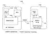
接下来参考图2,对根据本发明第一实施例的一种选通脉冲生成和解码系统200进行说明。注意,所述选通脉冲生成和解码系统示出了当一个设备使用多个内部状态机时的方案。状态机是下述的任意设备:在给定时刻存储某物的状态、并且能够对输入进行操作以改变所述状态、和/或对于任意给定变化引起动作或输出。RFIC上的状态机的主要功能是对校准、RX和TX事件进行控制和定时。Referring next to FIG. 2 , a strobe pulse generation and
基带控制器210包括选通脉冲生成和解码系统200,例如BBIC的基带控制器,其包括两个层1定时器(Layer-1timer)215和220,所述定时器可操作地耦合到用于生成选通脉冲信号227的选通脉冲生成器225。在移动通信终端中使用基带处理器中的层1定时器功能。其用于对各个移动协议的空中接口上的事件正确地定时。根据ISO 7层模型的定义,层1是物理层控制。层1定时器块是可编程定时器,其功能是用于在预编程的时间上生成中断。该中断将在移动终端中的软件或任意硬编码状态机中触发预期的事件。诸如RFIC那样的相应接收设备230或元件或IC包括选通脉冲解码器系统245,其可操作地耦合到两个对应的各个状态机235和240。
注意,选通脉冲生成器225对选通脉冲信号进行多路复用并将它们作为单个多路复用选通脉冲信号227以越过控制接口而传送到选通脉冲解码系统245。基带控制器210上的一个或两个层1定时器215、220被构造为触发选通脉冲生成器225以在单个信号上生成用于多路复用的各个选通脉冲信号。有利的是,可以设想,能够在一选通脉冲信号上对不同的选通脉冲振幅和/或不同的选通脉冲代码或选通脉冲脉宽进行多路复用。Note that the
优选的是,在可变的选通脉冲代码实施中,选通脉冲代码具有特定的脉冲宽度,其包括特定数字或1和0的序列,用以指示是哪个层1定时器210、215触发了选通脉冲生成器功能225并且指示接收设备230上的预期的状态机。Preferably, in a variable strobe code implementation, the strobe code has a specific pulse width that includes a specific number or sequence of 1s and 0s to indicate which
优选的是,可变选通脉冲振幅实施使用具有预定脉冲宽度并区分电压幅度等级的特定脉冲。然后由接收设备230接收多路复用选通脉冲信号227并在此由选通脉冲解码器245进行解码。然后根据选通脉冲振幅,被解码并被多路分离的选通脉冲信号触发设备230内部的内部状态机235、240中的一个或两个。Preferably, the variable strobe amplitude implementation uses specific pulses with predetermined pulse widths and differentiated voltage amplitude levels. Multiplexed
在该方式中,BBIC例如能够通过控制接口上的单个通信线路而发送多个不同的选通脉冲信号。例如,如果选通脉冲宽度在预定的容差范围内,那么选通脉冲接收设备或设备的子集被构造以对解码的选通脉冲输入生成响应或生成动作。预定容差是选通脉冲可变特征(也就是,脉冲宽度或振幅)的下限到上限。为了对选通脉冲进行解码,有关其额定值的磁滞是合理的,以便确保正确的解码。该磁滞将被定义在选通脉冲可变特性的预定容差范围内。In this way, the BBIC can, for example, send multiple different strobe signals over a single communication line on the control interface. For example, a strobe receiving device or subset of devices is configured to generate a response or generate an action in response to a decoded strobe input if the strobe width is within a predetermined tolerance range. The predetermined tolerance is a lower to upper limit on the variable characteristics (ie, pulse width or amplitude) of the strobe pulse. In order to decode the strobe, hysteresis is reasonable about its nominal value to ensure correct decoding. The hysteresis will be defined within a predetermined tolerance of the variable characteristics of the strobe.
接下来参考图3,根据本发明第二实施例示出了当多个设备340、350连接到基带控制器310时的选通脉冲和解码系统300。每一多路相应的接收设备(或者元件或IC,诸如RFIC)优选地包括选通脉冲解码器系统340、345,以及所述设备240、350内部的一个或多个状态机335、355。Referring next to FIG. 3, a strobe and
在该实施例中,基带控制器310上的层1定时器315、320的一个或两个能够再次触发选通脉冲生成器325。选通脉冲生成器325生成特定的多路复用的选通脉冲信号327(基于多个可变选通脉冲代码和/或选通脉冲振幅)。此外,选通脉冲生成器325通过控制接口而将多路复用选通脉冲信号327发送到设备340、350中的一个或多个。所述多路复用选通脉冲信号327被解码和多路分离成多路不同的选通脉冲信号,从而构造每一设备340、350以接收特定的选通脉冲信号327。如果对于各个设备340、350而言,选通脉冲信号327是有效的,那么该有效解码选通脉冲将触发内部设备的状态机335、355。In this embodiment, one or both of the
此外,可以设想,通过使用不同的选通脉冲代码和/或选通脉冲宽度和/或选通脉冲振幅而能够生成不同的选通脉冲信号。尽管通过使用用于在预期的接收状态机之间进行区别的这些特征中的任意一个特征来描述本发明的优选实施例,但是可以设想使用这些特征和任意其他合适的区别特征的组合。Furthermore, it is contemplated that different strobe signals can be generated by using different strobe codes and/or strobe widths and/or strobe amplitudes. Although the preferred embodiment of the invention has been described using any of these features for distinguishing between intended receive state machines, it is conceivable to use these features in combination with any other suitable distinguishing features.
在该方式中,BBIC能够通过控制接口上的单个线路而将多个不同的选通脉冲信号发送到多路接收设备、元件或IC。例如,通过确定特定选通脉冲信号的选通脉冲宽度是否处于预定的容差范围内,构造选通脉冲接收设备或设备的子集以对已解码的选通脉冲输入生成响应或生成动作。In this way, the BBIC is able to send multiple different strobe signals to multiple receiving devices, components or ICs via a single line on the control interface. For example, by determining whether the strobe width of a particular strobe signal is within a predetermined tolerance range, a strobe receiving device or subset of devices is configured to generate a response or generate an action to a decoded strobe input.
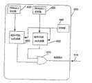
接下来参考图4,根据本发明的第三实施例来示出多路选通脉冲宽度或代码生成系统400。在本发明的第三实施例中,示出了两个层1定时器功能部件420、430(为清楚起见而仅示出了两个),由此,每一层1定时器功能部件420、430能够触发相应的脉冲代码(或脉冲宽度)生成器450、460。Referring next to FIG. 4, a multiplexed pulse width or
注意,有利的是,层1定时器420、430能够同时或独立地生成触发。这使得基带上的两个或多个L1定时器独立操作并不受选通脉冲生成机制约束成为可能。时钟源440优选地对脉冲代码生成器450、460进行时钟控制。相应的脉冲代码生成器450、460生成具有已知固定宽度(例如N个时钟周期宽)的代码脉冲。然后在功能470中将脉冲代码生成器450、460的每一输出进行逻辑组合以生成单个多路复用选通脉冲信号410以便经由耦合的控制接口而进行发送。Note that, advantageously, the
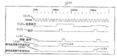
接下来参考图5,时序图500示出了根据图4中第三实施例的选通脉冲生成器波形(输入520、530和合成输出510)。如第一层1波形所示那样,第一层1定时器脉冲522触发脉冲代码生成器。脉冲代码生成器生成选通脉冲接口输出信号510,其包括用于指示层1定时器522已经触发了生成选通脉冲接口信号的特定代码540。同样,第二层1定时器输出532也触发(相应的)脉冲代码生成器。脉冲代码生成器生成选通脉冲接口输出信号510,其包括同样用于指示第二层1定时器脉冲532已经触发了生成选通脉冲接口信号的特定代码540。所以,优选的是,每一层1定时器生成单独的选通脉冲代码。如果层1定时器同时生成触发脉冲525、535,那么设想对脉冲代码生成器的两个输出进行逻辑组合以生成另外的特定的选通脉冲代码560。由层1所生成的选通脉冲优选地具有预定的宽度(例如“N”个时钟周期)。然而,可以设想根据实施,预定的脉冲宽度是可变的。Referring next to FIG. 5 , a timing diagram 500 shows strobe generator waveforms (inputs 520 , 530 and composite output 510 ) according to the third embodiment of FIG. 4 . As shown in the
接下来参考图6,示出了根据本发明第二或第三实施例的选通脉冲解码器布置600。在此,在控制接口上接收多路复用选通脉冲信号657并且将其输入到超时定时器630和选通脉冲解码器,所述选通脉冲解码器在该情况下为定时器选通脉冲(解码器)650、655。值得注意的是,为清楚起见而仅示出了两个选通脉冲解码器。超时定时器630和定时器选通脉冲(解码器)650、655由可定位在或不定位在接收设备、元件或IC内部的时钟源615进行时钟控制。Referring next to Figure 6, there is shown a strobe decoder arrangement 600 according to a second or third embodiment of the present invention. Here, a multiplexed
在操作中,只有当所接收到的选通脉冲信号657对于所述特定的定时器选通脉冲解码器块而言是有效的情况下,相应的定时器选通脉冲(解码器)650、655才生成脉冲。然后将定时器选通脉冲解码器块的输出输入到寄存器/锁存器635、640。优选的是,在预定时间之后并且一旦检测到选通脉冲信号657,超时定时器630就生成锁存信号632。使用所述锁存信号632以将选通脉冲解码器输出使能/锁存到相应的寄存器/锁存器635、640。In operation, the corresponding timer strobe (decoder) 650, 655 is activated only if the received
如果对于相应的选通脉冲解码器块而言,所接收到的选通脉冲信号657是有效的话,那么寄存器/锁存器的输出637、642触发相应的状态机620、625。The
在定时器选通脉冲输出被锁存之后,超时定时器630生成脉冲清除信号634以清除选通脉冲解码器的输出。After the timer strobe output is latched, the
在该解码器的实施例中,优选的是,根据解码器的脉冲宽度输入,存在固定的解码时间。In an embodiment of the decoder it is preferred that there is a fixed decoding time depending on the pulse width input to the decoder.
接下来参考图7,根据图6的解码器实施例示出了多路复用选通脉冲生成信号及其解码的时序图700。第一波形示出了时钟源所生成的系统时钟710。第二波形720指示解码器的输入选通脉冲信号(也就是图6的选通选通脉冲信号652)。由每一定时器选通脉冲对每一输入选通脉冲信号进行解码以确定其是否为有效的选通脉冲信号,以便触发一个或全部内部状态机。注意,该选通脉冲信号描述了基于相应选通脉冲代码字而被构造的三种不同选通脉冲信号721、722、723。Referring next to FIG. 7 , a timing diagram 700 of a multiplexed strobe pulse generation signal and its decoding is shown according to the decoder embodiment of FIG. 6 . The first waveform shows the
第三波形示出了超时定时器所生成的锁存脉冲730,所述超时定时器也就是图6的超时定时器630。第四波形示出了清除_脉冲(clear_pulse)信号740,其用于对选通脉冲解码器和寄存器/锁存器的输出进行复位。最后,最后两个波形750、760示出了寄存器的输出,其用于触发状态机。The third waveform shows the
接下来参考图8,根据本发明第四实施例示出(基于选通脉冲电压幅度)选通脉冲生成电路800。如此构造选通脉冲生成和解码系统800以使得层1定时器820、830触发脉冲。该脉冲将触发特定的开关850、870,从而选择特定的电压基准。另外,经由组合逻辑元件840来选择零电压基准860。输出被连接到输出缓冲器880以生成选通脉冲振幅信号882。Referring next to FIG. 8 , a gate pulse generation circuit 800 (based on gate pulse voltage magnitude) is shown in accordance with a fourth embodiment of the present invention. The strobe pulse generation and decoding system 800 is constructed such that the
第一电压基准(Vref1)870和第二电压基准(Vref2)850被设置到不同的电压电平。如果两个层1定时器820、830在同一时间触发,那么结果是组合Vref1 870和Vref2 850信号以用于在输出缓冲器880上生成第三电压电平,并且之后生成选通脉冲振幅信号882。A first voltage reference (Vref 1 ) 870 and a second voltage reference (Vref 2 ) 850 are set to different voltage levels. If two
选通脉冲幅度信号882的电压电平在控制接口的接收侧进行解码并且被解释为对应于耦合于此的两个(或更多)预期的状态机。The voltage levels of the
注意,设想基于落入预定窗口容差范围(也就是振幅上的+/-偏差)的选通脉冲的幅度,也能够对各个选通脉冲信号进行多路复用。Note that individual strobe signals can also be multiplexed envisaged based on the magnitude of the strobe pulses falling within a predetermined window tolerance range (ie +/- deviation in amplitude).
接下来参考图9,示出了根据图8的选通脉冲生成器电路的多路复用(不同幅度)的选通脉冲信号的时序图900。第一波形示出了由时钟源所生成的系统时钟910。示出了图8的两个层1定时器波形920、930。注意,在工作中,当第一层1定时器输出触发信号931时,(高)电压基准941被施加到输出选通脉冲。当第二层1定时器输出触发信号921时,第二(低)电压基准942被施加到输出选通脉冲940。另外,在两个层1定时器(也就是图8的层1定时器820、830)输出触发信号922、932的情况中,电压基准943的组合被施加到输出选通脉冲940。Referring next to FIG. 9 , a timing diagram 900 of multiplexed (different amplitude) strobe signals in accordance with the strobe generator circuit of FIG. 8 is shown. The first waveform shows the system clock 910 generated by the clock source. Two
以该方式,通过特定的选通脉冲生成器能够生成表示不同电压幅度的多路复用选通脉冲信号并将其通过控制接口而进行发送,以及在接收设备中将其解释为对应于预期的状态机。In this way, a multiplexed strobe signal representing different voltage amplitudes can be generated by a specific strobe generator and sent through the control interface, and interpreted in the receiving device as corresponding to the desired state machine.
接下来参考图10,示出了一种被构造以对图8和图9的多路复用(不同幅度)选通脉冲信号进行解码的解码器1010的优选电路图1000。输入选通信号1077是两个比较器1060、1065的输入1070、1075,其中不同的电压电平Vref1和Vref2对每一比较器进行基准。比较器上所施加的基准电压Vref1和Vref2表示了控制接口上多电平选通脉冲信号的阈值逻辑电平。Referring next to FIG. 10 , there is shown a preferred circuit diagram 1000 of a
两个比较器1060、1065的输出经由解码逻辑功能部件1040而分别输入到寄存器/锁存器1045、1050。两个比较器1060、1065的输出也分别输入到组合逻辑功能部件1055,该组合逻辑功能部件1055将输出提供给锁存脉冲生成器1030。锁存脉冲生成器1030可操作地耦合到时钟源1015。The outputs of the two
在操作中,当比较器输出的信号1060、1065任一等于或大于电压基准Vref1和Vref2(也就是振幅上的+/-偏差)任意一个时,响应于组合逻辑1055的输出,锁存脉冲生成器1030触发锁存信号1035。其后,使用锁存信号1035以将解码逻辑功能1040的输出锁存到相应的寄存器/锁存器1045、1050。In operation, when either of the
在解码逻辑输出被锁存之后,锁存脉冲生成器1030生成脉冲清除信号1034以对各个寄存器/锁存器1045、1050进行复位。如果解码器1010接收了有效的选通脉冲信号1077,那么寄存器/锁存器1045、1050的输出触发相应的状态机1020、1025。The
可以设想,在又一实施例中,对于在两个(或多个)电压基准的组合被输入到解码器1010以便触发在所述设备范围内或多个设备之间的两个(或多个)状态机1020、1025的情况而言,包括另一(或多个)比较器是可能的。It is contemplated that, in yet another embodiment, for a combination of two (or more) voltage references to be input to the
接下来参考图11,示出了根据本发明的优选实施例图10的选通脉冲幅度解码器电路所使用的相关波形的时序图1100。第一波形示出了时钟源所生成的系统时钟1110。第二波形1120示出了所述设备的输入选通脉冲信号(也就是图10的输入选通脉冲信号1077)。第三波形1130示出了锁存脉冲生成器所生成的锁存脉冲。注意,将每一选通脉冲与电压基准Vref1和Vref2进行比较以确定选通脉冲信号是否是一种将对内部状态机1020、1025中的一个(或两个/全部)进行触发的有效信号。第四波形1140示出了所述的清除脉冲信号,其用于对各个寄存器/锁存器进行复位。最后两个波形1150、1160示出了寄存器1155、1165的输出,该输出用于触发状态机。Referring next to FIG. 11 , there is shown a timing diagram 1100 of correlation waveforms used by the strobe amplitude decoder circuit of FIG. 10 in accordance with a preferred embodiment of the present invention. The first waveform shows the
以该方式,包括不同幅度的信号的多路复用选通脉冲信号能够通过控制接口被接收并且由特定的接收设备被进行解码,并且在该接收设备中,对应于预期的状态机,对每一相应的多路复用选通脉冲信号进行解释。In this way, a multiplexed strobe signal comprising signals of different amplitudes can be received through the control interface and decoded by a specific receiving device, and in the receiving device, corresponding to the desired state machine, for each A corresponding multiplexed strobe signal is explained.
接下来参考图12,根据本发明的优选实施例示出了又一选通脉冲生成和解码系统1200,其中在RFIC上具有状态机,并且该RFIC具有能够对不同选通脉冲类型进行解码、但仅连接到单个状态机的选通脉冲解码器。Referring next to FIG. 12, yet another strobe generation and
注意,该又一选通脉冲生成和解码系统1200包括:具有选通脉冲解码器的RFIC上的状态机,所述选通脉冲解码器能够对不同选通脉冲类型进行解码、但仅连接到单个状态机1240。Note that this yet another strobe generation and
基带控制器1210包括选通脉冲生成和解码系统1200,例如BBIC的基带控制器包括可操作地与用于生成选通脉冲信号1227的选通脉冲生成器1225相耦合的层1定时器1225。选通脉冲生成器1225能够从MCU1220或者从层1定时器事件生成器1215接收输入并从而生成不同的选通脉冲类型。
诸如RFIC那样的相应的接收设备1230或元件或IC包括选通脉冲解码器系统1245,其可操作耦合到相应的各个状态机1240。A
注意,根据选通脉冲信号1227,设备1230上的状态机1240能够使用多个输入代码以确定多种状态转换。选通脉冲生成器1225根据输入源而对不同的选通脉冲类型进行编码。有利的是,可以设想,能够在选通脉冲信号上对不同的选通脉冲振幅和/或不同的选通脉冲代码或选通脉冲宽度进行多路复用。Note that, depending on the
上述实施例并非是能够实施此处所述本发明原理的唯一布置,对多路设备(例如收发器)的选通脉冲信号进行多路复用而受益、同时并不增加成本或复杂度或增加引脚量的其他体系结构也可以被实施。所述体系结构的实例是功率管理系统,其中L1定时事件触发诸如电源电量倾斜或低电池电压检测那样的功能。The embodiments described above are not the only arrangements in which the principles of the invention described herein can be implemented to benefit from multiplexing strobe signals for multiple devices (such as transceivers) without adding cost or complexity or adding Other architectures for pin counts can also be implemented. An example of such an architecture is a power management system where L1 timed events trigger functions such as power supply ramping or low battery voltage detection.
本领域技术人员也应当理解的是,尽管结合BBIC-RFIC接口而描述了上述原理,但是本发明的原理同样可应用到包括任意控制接口或包括控制接口的装置。而且,可以设想,本发明的原理不限于双3G-2.xG无线通信设备,而可以应用到能够支持选通脉冲信号的任意设备,例如支持蓝牙TM或超宽带正交频分多路复用(UWB OFDM)技术的无线通信设备。Those skilled in the art should also appreciate that although the above principles have been described in connection with a BBIC-RFIC interface, the principles of the present invention are equally applicable to devices comprising or comprising any control interface. Furthermore, it is contemplated that the principles of the present invention are not limited to dual 3G-2.xG wireless communication devices, but may be applied to any device capable of supporting strobe signals, such as Bluetooth™ or UWB Orthogonal Frequency Division Multiplexing (UWB OFDM) technology wireless communication equipment.
而且,可以设想,上述发明原理能够被应用到很多收发器体系结构和平台方案,也就是说,半导体制造商可以在独立RFIC和/或BBIC和/或任意其他的子系统元件的设计中应用本发明原理。Furthermore, it is conceivable that the principles of the invention described above can be applied to many transceiver architectures and platform solutions, that is, semiconductor manufacturers can apply the present invention in the design of stand-alone RFICs and/or BBICs and/or any other subsystem components. Principle of invention.
可以理解的是,如上所述的控制接口及其操作目的是提供一个或多个以下的优点:It will be appreciated that the control interface and its operation as described above is intended to provide one or more of the following advantages:
(i)通过改变选通脉冲宽度、应用选通选通脉冲代码或应用各种选通脉冲幅度或各个选通脉冲信号的其他区别特性,可以生成用于在预期的接收设备/状态机之间进行区分的不同选通脉冲信号;(i) By varying the strobe width, applying a strobe code, or applying various strobe amplitudes or other distinguishing characteristics of the individual strobe signals, it is possible to generate different strobe signals for differentiation;
(ii)可以在单个选通脉冲信号上对不同的选通脉冲信号进行多路复用;以及(ii) different strobe signals can be multiplexed on a single strobe signal; and
(iii)在接收设备中,根据各种选通脉冲幅度和/或选通脉冲宽度可以解码多路复用的选通信号,以便触发不同子系统中的特定事件。(iii) In the receiving device, the multiplexed strobe signal can be decoded according to various strobe amplitudes and/or strobe widths in order to trigger specific events in different subsystems.
所以,本发明为结合有控制接口的诸如移动电话的现有装置提供了好多优点。在移动电话的环境中,提供这样的控制接口会更少浪费宝贵的资源,其中所述控制接口在例如2.xG和/或3G无线通信设备中的RFIC和BBIC之间能够以上述方式支持对选通脉冲进行多路复用和多路分离/解码。此外,当与当前解决方案相比较时,所提议的控制接口使得无线设备在体积、成本和功率消耗方面上降低,因此为IC和无线通信设备制造商提供了显著的益处。Therefore, the present invention offers many advantages to existing devices such as mobile telephones incorporating a control interface. In the context of mobile telephony, it would be less of a waste of valuable resources to provide a control interface between RFIC and BBIC in, for example, 2.xG and/or 3G wireless communication devices capable of supporting communication in the manner described above. Strobe for multiplexing and demultiplexing/decoding. Furthermore, the proposed control interface enables wireless devices to be reduced in size, cost and power consumption when compared with current solutions, thus providing significant benefits to IC and wireless communication device manufacturers.
虽然以上描述了本发明特定和优选的实施,但是很明显的是,本领域技术人员能够很容易地对所述发明概念进行变化和修改。While specific and preferred implementations of the invention have been described above, it will be evident that variations and modifications of the inventive concept will readily occur to those skilled in the art.
综上所述,已经对这样一种在诸如无线通信设备中包含了控制接口的装置进行了说明,其中,基本上克服了现有技术的构造所带来的上述各种缺点。In summary, there has been described an apparatus including a control interface, such as in a wireless communication device, in which the above-mentioned various disadvantages of prior art configurations are substantially overcome.
Claims (15)
Applications Claiming Priority (1)
| Application Number | Priority Date | Filing Date | Title |
|---|---|---|---|
| PCT/EP2004/052070WO2006027026A1 (en) | 2004-09-07 | 2004-09-07 | Apparatus and control interface therefor |
Publications (2)
| Publication Number | Publication Date |
|---|---|
| CN101044467A CN101044467A (en) | 2007-09-26 |
| CN100541465Ctrue CN100541465C (en) | 2009-09-16 |
Family
ID=34958652
Family Applications (1)
| Application Number | Title | Priority Date | Filing Date |
|---|---|---|---|
| CN200480044264.1AExpired - Fee RelatedCN100541465C (en) | 2004-09-07 | 2004-09-07 | Device and integrated circuit for generating a plurality of different gate pulse signals |
Country Status (5)
| Country | Link |
|---|---|
| US (1) | US8982899B2 (en) |
| EP (1) | EP1805634A1 (en) |
| JP (1) | JP2008512907A (en) |
| CN (1) | CN100541465C (en) |
| WO (1) | WO2006027026A1 (en) |
Families Citing this family (38)
| Publication number | Priority date | Publication date | Assignee | Title |
|---|---|---|---|---|
| EP2068250B1 (en)* | 2007-06-08 | 2016-02-17 | Motorola Mobility LLC | Method and apparatuses for communicating a message received from a main processor to a peripheral device |
| US8854019B1 (en) | 2008-09-25 | 2014-10-07 | Rf Micro Devices, Inc. | Hybrid DC/DC power converter with charge-pump and buck converter |
| US9166471B1 (en) | 2009-03-13 | 2015-10-20 | Rf Micro Devices, Inc. | 3D frequency dithering for DC-to-DC converters used in multi-mode cellular transmitters |
| US8315576B2 (en) | 2009-05-05 | 2012-11-20 | Rf Micro Devices, Inc. | Capacitive compensation of cascaded directional couplers |
| JP5347709B2 (en)* | 2009-05-18 | 2013-11-20 | 富士通株式会社 | Wireless device |
| EP2490339A4 (en)* | 2009-10-14 | 2015-01-14 | Nec Corp | Wireless communication device and method for controlling the state between rfic and bbic thereof |
| US8548398B2 (en) | 2010-02-01 | 2013-10-01 | Rf Micro Devices, Inc. | Envelope power supply calibration of a multi-mode radio frequency power amplifier |
| US8538355B2 (en) | 2010-04-19 | 2013-09-17 | Rf Micro Devices, Inc. | Quadrature power amplifier architecture |
| US9900204B2 (en)* | 2010-04-20 | 2018-02-20 | Qorvo Us, Inc. | Multiple functional equivalence digital communications interface |
| US9362825B2 (en) | 2010-04-20 | 2016-06-07 | Rf Micro Devices, Inc. | Look-up table based configuration of a DC-DC converter |
| US8892063B2 (en) | 2010-04-20 | 2014-11-18 | Rf Micro Devices, Inc. | Linear mode and non-linear mode quadrature PA circuitry |
| US8989685B2 (en) | 2010-04-20 | 2015-03-24 | Rf Micro Devices, Inc. | Look-up table based configuration of multi-mode multi-band radio frequency power amplifier circuitry |
| US9553550B2 (en) | 2010-04-20 | 2017-01-24 | Qorvo Us, Inc. | Multiband RF switch ground isolation |
| US9214865B2 (en) | 2010-04-20 | 2015-12-15 | Rf Micro Devices, Inc. | Voltage compatible charge pump buck and buck power supplies |
| US9030256B2 (en) | 2010-04-20 | 2015-05-12 | Rf Micro Devices, Inc. | Overlay class F choke |
| US8958763B2 (en) | 2010-04-20 | 2015-02-17 | Rf Micro Devices, Inc. | PA bias power supply undershoot compensation |
| US9048787B2 (en) | 2010-04-20 | 2015-06-02 | Rf Micro Devices, Inc. | Combined RF detector and RF attenuator with concurrent outputs |
| US9184701B2 (en) | 2010-04-20 | 2015-11-10 | Rf Micro Devices, Inc. | Snubber for a direct current (DC)-DC converter |
| US8811921B2 (en) | 2010-04-20 | 2014-08-19 | Rf Micro Devices, Inc. | Independent PA biasing of a driver stage and a final stage |
| US9077405B2 (en) | 2010-04-20 | 2015-07-07 | Rf Micro Devices, Inc. | High efficiency path based power amplifier circuitry |
| US9008597B2 (en) | 2010-04-20 | 2015-04-14 | Rf Micro Devices, Inc. | Direct current (DC)-DC converter having a multi-stage output filter |
| US8942650B2 (en) | 2010-04-20 | 2015-01-27 | Rf Micro Devices, Inc. | RF PA linearity requirements based converter operating mode selection |
| US8983410B2 (en) | 2010-04-20 | 2015-03-17 | Rf Micro Devices, Inc. | Configurable 2-wire/3-wire serial communications interface |
| US8831544B2 (en) | 2010-04-20 | 2014-09-09 | Rf Micro Devices, Inc. | Dynamic device switching (DDS) of an in-phase RF PA stage and a quadrature-phase RF PA stage |
| US8842399B2 (en) | 2010-04-20 | 2014-09-23 | Rf Micro Devices, Inc. | ESD protection of an RF PA semiconductor die using a PA controller semiconductor die |
| US8913971B2 (en) | 2010-04-20 | 2014-12-16 | Rf Micro Devices, Inc. | Selecting PA bias levels of RF PA circuitry during a multislot burst |
| US8983407B2 (en) | 2010-04-20 | 2015-03-17 | Rf Micro Devices, Inc. | Selectable PA bias temperature compensation circuitry |
| US8942651B2 (en) | 2010-04-20 | 2015-01-27 | Rf Micro Devices, Inc. | Cascaded converged power amplifier |
| US8811920B2 (en) | 2010-04-20 | 2014-08-19 | Rf Micro Devices, Inc. | DC-DC converter semiconductor die structure |
| US8947157B2 (en) | 2010-04-20 | 2015-02-03 | Rf Micro Devices, Inc. | Voltage multiplier charge pump buck |
| US9577590B2 (en) | 2010-04-20 | 2017-02-21 | Qorvo Us, Inc. | Dual inductive element charge pump buck and buck power supplies |
| US9214900B2 (en) | 2010-04-20 | 2015-12-15 | Rf Micro Devices, Inc. | Interference reduction between RF communications bands |
| US9065505B2 (en) | 2012-01-31 | 2015-06-23 | Rf Micro Devices, Inc. | Optimal switching frequency for envelope tracking power supply |
| JP6060003B2 (en)* | 2013-02-21 | 2017-01-11 | パナソニック株式会社 | RADIO COMMUNICATION DEVICE AND METHOD FOR STARTING THE RADIO COMMUNICATION DEVICE |
| CN105068950A (en)* | 2015-07-24 | 2015-11-18 | 深圳市微纳集成电路与系统应用研究院 | Pin multiplexing system and method |
| US20170222686A1 (en)* | 2016-02-01 | 2017-08-03 | Qualcomm Incorporated | Scalable, high-efficiency, high-speed serialized interconnect |
| CN108702358B (en) | 2016-02-01 | 2020-12-08 | 高通股份有限公司 | Scalable Efficient High Speed Serialized Interconnect |
| US10159053B2 (en) | 2016-02-02 | 2018-12-18 | Qualcomm Incorporated | Low-latency low-uncertainty timer synchronization mechanism across multiple devices |
Family Cites Families (28)
| Publication number | Priority date | Publication date | Assignee | Title |
|---|---|---|---|---|
| JPS60121848A (en)* | 1983-12-05 | 1985-06-29 | Fujitsu Ltd | Inter-device communication method |
| FI79769C (en)* | 1988-06-10 | 1991-01-14 | Heikki Malkki | SNABBTELEFONSYSTEM SAMT FOERFARANDE FOER UPPKOPPLING I ETT SNABBTELEFONSYSTEM. |
| JP2850282B2 (en)* | 1994-07-06 | 1999-01-27 | 日本コロムビア株式会社 | Communication device |
| US5696685A (en)* | 1994-07-06 | 1997-12-09 | Pitney Bowes Inc. | Control system for an electronic postage meter having a programmable print head controller |
| JPH0822394A (en)* | 1994-07-08 | 1996-01-23 | Minolta Co Ltd | Signal processor |
| US5757857A (en)* | 1994-07-21 | 1998-05-26 | The Regents Of The University Of California | High speed self-adjusting clock recovery circuit with frequency detection |
| US5721733A (en)* | 1995-10-13 | 1998-02-24 | General Wireless Communications, Inc. | Wireless network access scheme |
| CN1142709A (en) | 1996-03-06 | 1997-02-12 | 李永焜 | Carrier amplituding method controlled by keys and models therefor |
| GB2324688A (en)* | 1997-04-25 | 1998-10-28 | Motorola Ltd | A modem in which bit rate is determined using the width of a start bit |
| JPH11215018A (en)* | 1998-01-20 | 1999-08-06 | Matsushita Electric Ind Co Ltd | Antenna device |
| US6385208B1 (en)* | 1998-06-02 | 2002-05-07 | Cisco Technology, Inc. | Serial media independent interface |
| JP2000324200A (en) | 1999-05-14 | 2000-11-24 | Mitsubishi Electric Corp | Interface circuit |
| US6490638B1 (en)* | 1999-08-23 | 2002-12-03 | Advanced Micro Devices, Inc. | General purpose bus with programmable timing |
| JP4303373B2 (en)* | 1999-09-14 | 2009-07-29 | 株式会社日立コミュニケーションテクノロジー | Wireless base station equipment |
| JP2002082830A (en) | 2000-02-14 | 2002-03-22 | Mitsubishi Electric Corp | Interface circuit |
| US6980563B2 (en)* | 2000-04-13 | 2005-12-27 | International Business Machines Corporation | Method and system for fast ethernet serial port multiplexing to reduce I/O pin count |
| US6597459B2 (en)* | 2000-05-16 | 2003-07-22 | Zygo Corporation | Data age adjustments |
| JP3802352B2 (en)* | 2001-01-24 | 2006-07-26 | 三洋電機株式会社 | Driving IC and optical print head |
| JP2002280904A (en)* | 2001-03-22 | 2002-09-27 | Hitachi Ltd | Analog multiplex transmission equipment |
| US6671211B2 (en) | 2001-04-17 | 2003-12-30 | International Business Machines Corporation | Data strobe gating for source synchronous communications interface |
| DE10136853B4 (en) | 2001-07-27 | 2004-11-18 | Infineon Technologies Ag | Method for data communication of several semiconductor memory modules with a controller module and semiconductor memory module set up for this |
| CN100424506C (en) | 2001-10-17 | 2008-10-08 | 中国石油天然气管道科学研究院 | Phased array ultrasonic instrument and its detection method |
| JP3973017B2 (en)* | 2002-02-14 | 2007-09-05 | 富士通株式会社 | Radio receiver for estimating interference power |
| US7792089B2 (en)* | 2002-07-31 | 2010-09-07 | Cattron-Theimeg, Inc. | System and method for wireless remote control of locomotives |
| TW566011B (en)* | 2002-09-23 | 2003-12-11 | Ind Tech Res Inst | Dual mode receiving method and device |
| JP3990974B2 (en)* | 2002-11-26 | 2007-10-17 | 株式会社日立コミュニケーションテクノロジー | Peak factor reduction device |
| US7206878B2 (en)* | 2003-01-08 | 2007-04-17 | International Business Machines Corporation | Voltage level bus protocol for transferring data |
| US20050138535A1 (en)* | 2003-12-02 | 2005-06-23 | Sivagnanam Parthasarathy | Method and system for branch metric calculation in a viterbi decoder |
- 2004
- 2004-09-07CNCN200480044264.1Apatent/CN100541465C/ennot_activeExpired - Fee Related
- 2004-09-07JPJP2007530593Apatent/JP2008512907A/enactivePending
- 2004-09-07USUS11/574,867patent/US8982899B2/ennot_activeExpired - Fee Related
- 2004-09-07WOPCT/EP2004/052070patent/WO2006027026A1/ennot_activeApplication Discontinuation
- 2004-09-07EPEP04766728Apatent/EP1805634A1/ennot_activeWithdrawn
Also Published As
| Publication number | Publication date |
|---|---|
| CN101044467A (en) | 2007-09-26 |
| JP2008512907A (en) | 2008-04-24 |
| EP1805634A1 (en) | 2007-07-11 |
| US20090274207A1 (en) | 2009-11-05 |
| US8982899B2 (en) | 2015-03-17 |
| WO2006027026A1 (en) | 2006-03-16 |
Similar Documents
| Publication | Publication Date | Title |
|---|---|---|
| CN100541465C (en) | Device and integrated circuit for generating a plurality of different gate pulse signals | |
| AU2013270396B2 (en) | A multiformat digital audio interface | |
| US11114112B2 (en) | Low power, high bandwidth, low latency data bus | |
| EP2856690B1 (en) | Universal synchronization engine based on probabilistic methods for guarantee of lock in multiformat audio systems | |
| US8473000B2 (en) | Communication device, integrated circuit and method therefor | |
| CN101467383B (en) | A glitch-free clock signal multiplexer circuit and method of operation thereof | |
| JP7293257B2 (en) | Low power, high bandwidth, low latency data bus | |
| US9596669B2 (en) | Method and apparatus for transmitting data | |
| JPH0675680A (en) | Key pad scanner mechanism and method for scanning key pad | |
| US7747238B2 (en) | Wireless communication device and data interface | |
| US8923465B2 (en) | Method for sampling data and apparatus therefor | |
| EP0580337A2 (en) | Pull-up disable mechanisms for microcontrollers in integrated circuits | |
| JPH06195478A (en) | Integrated circuit | |
| US8306172B2 (en) | Electronic device, integrated circuit and method therefor | |
| HK1206135B (en) | A multiformat digital audio interface | |
| HK1203712B (en) | Universal synchronization engine based on probabilistic methods for guarantee of lock in multiformat audio systems |
Legal Events
| Date | Code | Title | Description |
|---|---|---|---|
| C06 | Publication | ||
| PB01 | Publication | ||
| C10 | Entry into substantive examination | ||
| SE01 | Entry into force of request for substantive examination | ||
| C14 | Grant of patent or utility model | ||
| GR01 | Patent grant | ||
| CF01 | Termination of patent right due to non-payment of annual fee | Granted publication date:20090916 Termination date:20180907 | |
| CF01 | Termination of patent right due to non-payment of annual fee |