CN100539074C - The manufacture method of dual-damascene structure - Google Patents
The manufacture method of dual-damascene structureDownload PDFInfo
- Publication number
- CN100539074C CN100539074CCNB2007100403801ACN200710040380ACN100539074CCN 100539074 CCN100539074 CCN 100539074CCN B2007100403801 ACNB2007100403801 ACN B2007100403801ACN 200710040380 ACN200710040380 ACN 200710040380ACN 100539074 CCN100539074 CCN 100539074C
- Authority
- CN
- China
- Prior art keywords
- layer
- bottom anti
- connecting hole
- barrier layer
- reflection
- Prior art date
- Legal status (The legal status is an assumption and is not a legal conclusion. Google has not performed a legal analysis and makes no representation as to the accuracy of the status listed.)
- Expired - Fee Related
Links
- 238000000034methodMethods0.000titleclaimsabstractdescription46
- 238000004519manufacturing processMethods0.000titleclaimsabstractdescription21
- 230000004888barrier functionEffects0.000claimsabstractdescription65
- 238000005530etchingMethods0.000claimsabstractdescription45
- 239000004065semiconductorSubstances0.000claimsabstractdescription31
- 239000000758substrateSubstances0.000claimsabstractdescription23
- 239000007769metal materialSubstances0.000claimsdescription5
- 239000002184metalSubstances0.000abstractdescription36
- 229910052751metalInorganic materials0.000abstractdescription36
- 239000010410layerSubstances0.000description230
- 230000009977dual effectEffects0.000description27
- 230000003667anti-reflective effectEffects0.000description19
- 229920002120photoresistant polymerPolymers0.000description13
- 239000011229interlayerSubstances0.000description10
- XUIMIQQOPSSXEZ-UHFFFAOYSA-NSiliconChemical compound[Si]XUIMIQQOPSSXEZ-UHFFFAOYSA-N0.000description6
- 239000010703siliconSubstances0.000description6
- 229910052710siliconInorganic materials0.000description6
- 239000006117anti-reflective coatingSubstances0.000description5
- 239000000463materialSubstances0.000description5
- 238000010586diagramMethods0.000description4
- 239000010949copperSubstances0.000description3
- VYPSYNLAJGMNEJ-UHFFFAOYSA-Nsilicon dioxideInorganic materialsO=[Si]=OVYPSYNLAJGMNEJ-UHFFFAOYSA-N0.000description3
- RYGMFSIKBFXOCR-UHFFFAOYSA-NCopperChemical compound[Cu]RYGMFSIKBFXOCR-UHFFFAOYSA-N0.000description2
- 229910052581Si3N4Inorganic materials0.000description2
- 229910052802copperInorganic materials0.000description2
- 230000007547defectEffects0.000description2
- 239000003989dielectric materialSubstances0.000description2
- 239000011521glassSubstances0.000description2
- HQVNEWCFYHHQES-UHFFFAOYSA-Nsilicon nitrideChemical compoundN12[Si]34N5[Si]62N3[Si]51N64HQVNEWCFYHHQES-UHFFFAOYSA-N0.000description2
- 229910004298SiO 2Inorganic materials0.000description1
- 229910052782aluminiumInorganic materials0.000description1
- XAGFODPZIPBFFR-UHFFFAOYSA-NaluminiumChemical compound[Al]XAGFODPZIPBFFR-UHFFFAOYSA-N0.000description1
- 238000005229chemical vapour depositionMethods0.000description1
- 239000004020conductorSubstances0.000description1
- 238000007796conventional methodMethods0.000description1
- 238000005336crackingMethods0.000description1
- 239000010432diamondSubstances0.000description1
- 238000001312dry etchingMethods0.000description1
- 230000003628erosive effectEffects0.000description1
- 229940104869fluorosilicateDrugs0.000description1
- 238000012986modificationMethods0.000description1
- 230000004048modificationEffects0.000description1
- 239000011295pitchSubstances0.000description1
- 150000003376siliconChemical class0.000description1
- 235000012239silicon dioxideNutrition0.000description1
- 239000000377silicon dioxideSubstances0.000description1
- 238000001039wet etchingMethods0.000description1
Images


Landscapes
- Internal Circuitry In Semiconductor Integrated Circuit Devices (AREA)
Abstract
Description
Translated fromChinese技术领域technical field
本发明涉及半导体制作技术领域,特别涉及一种双镶嵌结构(dualdamascene structure)的制作方法。The invention relates to the technical field of semiconductor manufacturing, in particular to a method for manufacturing a dual damascene structure.
背景技术Background technique
当今半导体器件制作技术飞速发展,半导体器件已经具有深亚微米结构,集成电路中包含巨大数量的半导体元件。在如此大规模集成电路中,元件之间的高性能、高密度的连接不仅在单个互连层中互连,而且要在多层之间进行互连。因此,通常提供多层互连结构,其中多个互连层互相堆叠,并且层间绝缘膜置于其间,用于连接半导体元件。特别是利用双镶嵌(dual-damascene)工艺形成的多层互连结构,其预先在层间绝缘膜中形成沟槽(trench)和连接孔(via),然后用导电材料例如铜(Cu)填充所述沟槽和连接孔。例如申请号为02106882.8的中国专利申请文件提供的双镶嵌制作工艺,这种互连结构和互连工艺已经在集成电路制作中得到广泛应用。Today's semiconductor device manufacturing technology is developing rapidly, semiconductor devices already have a deep submicron structure, and integrated circuits contain a huge number of semiconductor components. In such large-scale integrated circuits, high-performance, high-density connections between components are not only interconnected in a single interconnect layer, but also interconnected between multiple layers. Therefore, a multilayer interconnection structure is generally provided in which a plurality of interconnection layers are stacked on each other with an interlayer insulating film interposed therebetween for connecting semiconductor elements. In particular, a multilayer interconnection structure formed using a dual-damascene process, which preforms a trench (trench) and a connection hole (via) in an interlayer insulating film, and then fills it with a conductive material such as copper (Cu) The grooves and connecting holes. For example, the dual damascene manufacturing process provided by the Chinese patent application document with application number 02106882.8, this interconnection structure and interconnection process has been widely used in the manufacture of integrated circuits.
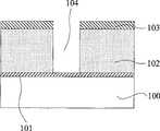
附图1至附图6为现有技术双镶嵌结构的制作方法的结构示意图,如图1所示,提供半导体衬底100,所述半导体衬底内含有金属布线,在半导体衬底100上形成覆盖层101,并在覆盖层101上形成内层介电层102(inter-layerdielectrics;ILD),所述内层介电层材料如氟硅玻璃和低介电常数材料等。所述覆盖层101可防止半导体衬底100中的金属布线扩散到内层介电层102中,亦可防止刻蚀过程中半导体衬底100中的金属布线被刻蚀。之后,在内层介电层102上形成阻挡层103,所述阻挡层103的作用在于光刻胶曝光显影过程中避免光线透过,随后,在阻挡层103上形成光刻胶层,并在光刻胶上形成开口,开口位置即为需要形成双镶嵌结构的位置,随后以光刻胶为掩膜,刻蚀阻挡层103、内层介电层102直至暴露出覆盖层101,在阻挡层103和内层介电层102中形成连接孔104。
参考附图2所示,在阻挡层103上以及连接孔104中形成覆盖内层介电层102的底部抗反射层(Bottom Anti-Reflective Coating,BARC)105。参考附图3所示,刻蚀底部抗反射层105,直至完全去除阻挡层103上的底部抗反射层105,并保留开口104内的部分底部抗反射层105,其中连接孔104内的底部抗反射层105的厚度应该保证在随后刻蚀连接孔104形成双镶嵌结构的工艺过程中避免覆盖层101被刻蚀穿。Referring to FIG. 2 , a bottom anti-reflective coating (Bottom Anti-Reflective Coating, BARC) 105 covering the
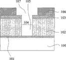
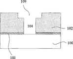
参考附图4所示,在阻挡层103上形成光刻胶层106,并通过曝光、显影在光刻胶层106上形成开口107,开口107的位置与开口104的位置对应,并且开口的宽度大于开口104的宽度。参考附图5所示,以光刻胶层106为掩膜,刻蚀阻挡层103以及内层介电层102,形成沟槽109。参考附图6所示,去除阻挡层103、光刻胶层106以及连接孔104内的底部抗反射层105,并刻蚀连接孔104内的覆盖层101,直至暴露出半导体衬底100,形成附图6所示的双镶嵌结构。Referring to shown in accompanying drawing 4, form
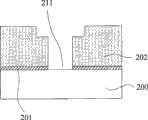
通常的金属布线结构的俯视图如图7所示,图中1为半导体衬垫(pad)上沟槽的俯视图,图中各个沟槽之间均匀间隔。随着技术发展,半导体器件的尺寸越来越小,含有的器件越来越多,因此,为了满足层与层间黏附力的要求,产生了各种各样的衬垫(pad)布线结构。例如形成网格状衬垫(mesh pad)布线结构,这种网格状衬垫布线结构内需要形成密集的沟槽,如图8所示为网格状衬垫布线结构的密集的沟槽的结构俯视图,图中2为半导体衬垫(pad)上沟槽的俯视图,图9为同时含有常规的布线结构和含有网格状衬垫布线结构的剖面结构示意图,图中10为半导体衬底,所述半导体衬底10上还有常规的布线结构区域11以及网格状衬垫布线结构区域22,半导体衬底10上含有覆盖层20,覆盖层20上含有内层介电层30,在内层介电层30上与常规的布线结构区域11对应的位置形成有第一连接孔40,与网格状衬垫布线结构区域22对应的位置形成有第二连接孔50,在采用附图1至附图6所示的形成双镶嵌结构的方法制作双镶嵌结构时,由于第二连接孔50比较密集,而且第二连接孔50宽度较小,底部抗反射层不容易填满第二连接孔50,因此,在随后刻蚀底部抗反射层的过程中,第二连接孔50内剩余的底部抗反射层的厚度就会远小于第一连接孔40内的底部抗反射层的厚度,甚至出现第二连接孔50内的底部抗反射层被完全刻蚀的现象,这就导致在随后刻蚀底部抗反射层形成沟槽的工艺中刻蚀到覆盖层20,最终导致在沟槽和连接孔内形成金属布线之后覆盖层20和内层介电层30之间黏附力变差而开裂。A top view of a common metal wiring structure is shown in FIG. 7 , and 1 in the figure is a top view of grooves on a semiconductor pad (pad), and the grooves in the figure are evenly spaced. With the development of technology, the size of semiconductor devices is getting smaller and more devices are included. Therefore, in order to meet the requirements of layer-to-layer adhesion, various pad wiring structures have been produced. For example, a mesh pad wiring structure is formed, and dense grooves need to be formed in the mesh pad wiring structure, as shown in FIG. 8 . The top view of the structure, 2 in the figure is the top view of the trench on the semiconductor pad (pad), and FIG. 9 is a schematic cross-sectional structure diagram containing both a conventional wiring structure and a grid pad wiring structure. 10 in the figure is a semiconductor substrate. The
发明内容Contents of the invention
因此,本发明的目的在于提供一种双镶嵌结构的制作方法,在半导体衬底上同时含有密集的金属布线结构和常规的金属布线结构时,能够避免在沟槽和连接孔内形成金属布线之后覆盖层和内层介电层之间开裂。Therefore, the object of the present invention is to provide a kind of fabrication method of dual damascene structure, when the semiconductor substrate contains dense metal wiring structure and conventional metal wiring structure at the same time, can avoid the metal wiring after forming in trench and connection hole. Cracking between cover and inner dielectric layers.
为达到上述目的,本发明提供了一种双镶嵌结构的制作方法,包括:In order to achieve the above object, the present invention provides a method for manufacturing a dual damascene structure, comprising:
在半导体衬底上依次形成覆盖层、内层介质层和阻挡层;sequentially forming a cover layer, an inner dielectric layer and a barrier layer on the semiconductor substrate;
刻蚀内层介质层和阻挡层形成连接孔,所述连接孔暴露出覆盖层;Etching the inner dielectric layer and the barrier layer to form a connection hole, the connection hole exposes the cover layer;
在连接孔内以及阻挡层上形成第一底部抗反射层;forming a first bottom anti-reflection layer in the connection hole and on the barrier layer;
刻蚀第一底部抗反射层,直至阻挡层上的第一底部抗反射层被完全去除,同时会刻蚀连接孔内的第一底部抗反射层,暴露出连接孔的开口;Etching the first bottom anti-reflection layer until the first bottom anti-reflection layer on the barrier layer is completely removed, and at the same time etching the first bottom anti-reflection layer in the connection hole to expose the opening of the connection hole;
在连接孔内以及阻挡层上形成第二底部抗反射层;forming a second bottom anti-reflective layer in the connection hole and on the barrier layer;
刻蚀第二底部抗反射层,形成第三底部抗反射层,所述第三底部抗反射层位于连接孔内;Etching the second bottom anti-reflection layer to form a third bottom anti-reflection layer, the third bottom anti-reflection layer is located in the connection hole;
刻蚀阻挡层和内层介质层形成沟槽,沟槽的位置与连接孔的位置对应并与连接孔连通;The etch barrier layer and the inner dielectric layer form a trench, the position of the trench corresponds to the position of the connection hole and communicates with the connection hole;
去除阻挡层和第三底部抗反射层,并去除连接孔内的覆盖层直至暴露半导体衬底,形成双镶嵌结构;removing the barrier layer and the third bottom anti-reflection layer, and removing the cover layer in the connection hole until the semiconductor substrate is exposed, forming a dual damascene structure;
在双镶嵌结构内填充金属材料。Metal material is filled in the dual damascene structure.
其中,所述连接孔的间距大小不同,尤其是,所述连接孔在部分区域呈网格状衬垫分布。Wherein, the pitches of the connection holes are different, especially, the connection holes are distributed in grid-like pads in some areas.
所述刻蚀阻挡层和内层介质层形成沟槽后,第三底部抗反射层的厚度大于等于0。进一步,所述第三底部抗反射层的厚度为500~1000
与现有技术相比,本发明具有以下优点:Compared with the prior art, the present invention has the following advantages:
1、本发明提供一种双镶嵌结构的制作方法,在连接孔内形成第一底部抗反射层,然后进行刻蚀,去除阻挡层上的第一底部抗反射层,同时会刻蚀连接孔内的第一底部抗反射层,暴露出连接孔的开口,再次在连接孔内形成第二底部抗反射层,并进行刻蚀,完全去除阻挡层上的底部抗反射层并去除连接孔内的部分第二底部抗反射层,形成第三底部抗反射层,所述双镶嵌结构的制作方法2次形成底部抗反射层,并进行2次刻蚀,降低了密集的金属布线结构区域和常规的金属布线结构区域连接孔内形成的第二底部抗反射层的厚度差,避免在随后刻蚀介电层形成沟槽的工艺过程中,密集的布线结构中连接孔内的底部抗反射层被过刻蚀,甚至刻蚀至覆盖层,最终导致连接孔和沟槽内形成金属布线之后在覆盖层和内层介电层之间产生剥离的缺陷。1. The present invention provides a method for manufacturing a dual damascene structure, forming a first bottom antireflection layer in a connection hole, and then performing etching to remove the first bottom antireflection layer on the barrier layer, and at the same time etch the bottom antireflection layer in the connection hole The first bottom anti-reflective layer, exposing the opening of the connection hole, forming the second bottom anti-reflective layer in the connection hole again, and performing etching, completely removing the bottom anti-reflection layer on the barrier layer and removing the part inside the connection hole The second bottom anti-reflection layer forms the third bottom anti-reflection layer. The manufacturing method of the dual damascene structure forms the bottom anti-reflection layer twice and performs etching twice, which reduces the dense metal wiring structure area and the conventional metal The difference in thickness of the second bottom anti-reflection layer formed in the connection hole in the wiring structure area avoids over-etching of the bottom anti-reflection layer in the connection hole in the dense wiring structure during the subsequent process of etching the dielectric layer to form a trench Etching, even etching to the capping layer, eventually leads to the defect of peeling between the capping layer and the inner dielectric layer after the metal wiring is formed in the contact hole and the trench.
2、本发明是在现有刻蚀工艺的基础上,增加一次形成底部抗反射层并进行刻蚀的工艺,对现有双镶嵌结构的制作工艺影响不大,提高了工艺的兼容性,并且避免了现有技术的缺陷。2. On the basis of the existing etching process, the present invention adds a process of forming the bottom anti-reflection layer and performing etching, which has little influence on the existing dual damascene structure manufacturing process, improves the compatibility of the process, and The defects of the prior art are avoided.
附图说明Description of drawings
图1至图6为说明现有制作双镶嵌结构方法的剖面示意图;1 to 6 are schematic cross-sectional views illustrating a conventional method for fabricating a dual damascene structure;
图7为现有技术金属布线结构的俯视图;7 is a top view of a prior art metal wiring structure;
图8为网格状衬垫布线结构的密集的沟槽的结构俯视图;FIG. 8 is a structural top view of dense trenches in a grid-like pad wiring structure;
图9为同时含有常规的布线结构和含有网格状衬垫布线结构的剖面结构示意图;FIG. 9 is a schematic diagram of a cross-sectional structure including both a conventional wiring structure and a grid-like pad wiring structure;
图10至图17为根据本发明实施例1的双镶嵌结构制作方法的剖面示意图;10 to 17 are schematic cross-sectional views of a method for fabricating a dual damascene structure according to
图18为本发明实施例1双镶嵌结构制作方法的工艺流程图。FIG. 18 is a process flow diagram of the method for fabricating a dual damascene structure according to
具体实施方式Detailed ways
为使本发明的上述目的、特征和优点能够更加明显易懂,下面结合附图对本发明的具体实施方式做详细的说明。In order to make the above objects, features and advantages of the present invention more comprehensible, specific implementations of the present invention will be described in detail below in conjunction with the accompanying drawings.
实施例1Example 1
本发明的本质在于提供一种双镶嵌结构的制作方法,首先在连接孔内形成第一底部抗反射层,然后进行刻蚀,去除阻挡层上的第一底部抗反射层,再次在连接孔内形成第二底部抗反射层,并进行刻蚀,完全去除阻挡层上的底部抗反射层并去除连接孔内的部分第二底部抗反射层,形成第三底部抗反射层,第三底部抗反射层的厚度应该保证在随后形成沟槽的的工艺过程中避免覆盖层被刻蚀穿。The essence of the present invention is to provide a method for manufacturing a dual damascene structure. First, a first bottom anti-reflection layer is formed in the connection hole, and then etching is performed to remove the first bottom anti-reflection layer on the barrier layer. Forming the second bottom anti-reflection layer, and performing etching, completely removing the bottom anti-reflection layer on the barrier layer and removing part of the second bottom anti-reflection layer in the connection hole, forming a third bottom anti-reflection layer, and the third bottom anti-reflection layer The thickness of the layer should ensure that the cover layer is not etched through during the subsequent process of forming the trench.
所述双镶嵌结构的制作方法避免现有技术中在同时含有密集的金属布线结构和常规的金属布线结构时,由于密集的布线结构中连接孔过于密集使底层抗反射层不容易填满连接孔,在连接孔内形成孔洞,刻蚀去除介电层上的底部抗反射层之后,使密集的布线结构中连接孔内底部抗反射层的厚度小于常规的布线结构中连接孔内底部抗反射层的厚度,在随后刻蚀介电层形成沟槽的工艺过程中,密集的布线结构中连接孔内的底部抗反射层被过刻蚀,甚至刻蚀至覆盖层,最终导致连接孔和沟槽内形成金属布线之后在覆盖层和内层介电层之间产生剥离的现象。The manufacturing method of the dual damascene structure avoids that in the prior art, when the dense metal wiring structure and the conventional metal wiring structure are contained at the same time, the underlying antireflection layer is not easy to fill the connection holes because the connection holes in the dense wiring structure are too dense. , forming a hole in the connection hole, after etching and removing the bottom anti-reflection layer on the dielectric layer, the thickness of the bottom anti-reflection layer in the connection hole in the dense wiring structure is smaller than that in the conventional wiring structure. During the subsequent process of etching the dielectric layer to form trenches, the bottom anti-reflective layer in the connection holes in the dense wiring structure is over-etched, even etched to the cover layer, resulting in connection holes and trenches The peeling phenomenon occurs between the cover layer and the inner dielectric layer after the inner metal wiring is formed.
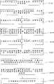
本发明提供了一种双镶嵌结构的制作方法,参考附图18,包括:步骤S101,在半导体衬底上依次形成覆盖层、内层介质层和阻挡层;步骤S102,刻蚀内层介质层和阻挡层形成连接孔,所述连接孔暴露出覆盖层;步骤S103,在连接孔内以及阻挡层上形成第一底部抗反射层;步骤S104,刻蚀第一底部抗反射层,直至阻挡层上的第一底部抗反射层被完全去除,同时会刻蚀连接孔内的第一底部抗反射层,暴露出连接孔的开口;步骤S105,在连接孔内以及阻挡层上形成第二底部抗反射层;步骤S106,刻蚀第二底部抗反射层,形成第三底部抗反射层,所述第三底部抗反射层位于连接孔内;步骤S107,刻蚀阻挡层和内层介质层形成沟槽,沟槽的位置与连接孔的位置对应并与连接孔连通;步骤S108,去除阻挡层和第三底部抗反射层,并去除连接孔内的覆盖层直至暴露半导体衬底,形成双镶嵌结构;步骤S109,在双镶嵌结构内填充金属材料。The present invention provides a method for fabricating a dual damascene structure. Referring to FIG. 18 , it includes: step S101, sequentially forming a covering layer, an inner dielectric layer, and a barrier layer on a semiconductor substrate; step S102, etching the inner dielectric layer Form a connection hole with the barrier layer, and the connection hole exposes the cover layer; step S103, form a first bottom anti-reflection layer in the connection hole and on the barrier layer; step S104, etch the first bottom anti-reflection layer until the barrier layer The first bottom anti-reflective layer on the top is completely removed, and at the same time, the first bottom anti-reflective layer in the connection hole will be etched to expose the opening of the connection hole; step S105, forming a second bottom anti-reflective layer in the connection hole and on the barrier layer Reflective layer; Step S106, etching the second bottom anti-reflective layer to form a third bottom anti-reflective layer, the third bottom anti-reflective layer is located in the connection hole; Step S107, etching the barrier layer and the inner dielectric layer to form a groove groove, the position of the groove corresponds to the position of the connection hole and communicates with the connection hole; step S108, removes the barrier layer and the third bottom anti-reflection layer, and removes the cover layer in the connection hole until the semiconductor substrate is exposed, forming a dual damascene structure ; Step S109, filling metal material in the dual damascene structure.
以下通过图10至图17对本发明双镶嵌结构制作方法做详细的说明。The method for fabricating the dual damascene structure of the present invention will be described in detail below with reference to FIGS. 10 to 17 .
如图10所示,提供半导体衬底200,所述半导体衬底内含有金属布线,在半导体衬底200上形成覆盖层201,并在覆盖层201上形成内层介电层202(inter-layer dielectrics;ILD),内层介电层202的厚度为1000-20000
所述覆盖层201的材料例如氮化硅(Si3N4)或氮氧化硅(SiON)或氮碳氧化硅(SiCNO)等,可防止半导体衬底200中的金属布线扩散到内层介电层202中,亦可作为刻蚀停止层,防止后续刻蚀过程中半导体衬底200中的金属布线被刻蚀。之后,在内层介电层202上形成阻挡层203,所述阻挡层203的材料例如氮化硅、氮氧化硅等,主要作用在于光刻胶曝光显影过程中避免光线透过,随后,在阻挡层203上形成光刻胶层(图中未示出),并在光刻胶上形成开口,开口位置即为需要形成双镶嵌结构的位置,随后以光刻胶为掩膜,刻蚀阻挡层203、内层介电层202直至暴露出覆盖层201,在阻挡层203和内层介电层202中形成连接孔204。The material of the
参考附图11所示,在连接孔204中以及阻挡层203上形成第一底部抗反射层(Bottom Anti-Reflective Coating,BARC)205。所述第一底部抗反射层205应尽可能填满连接孔204,在阻挡层203表面上的厚度为1000
由于本实施例双镶嵌结构的制作方法较多的应用于同时含有密集的金属布线结构和常规的金属布线结构,所述密集的金属布线结构例如排布比较密集的网格状布线结构(mesh pad),在这种网格状布线结构中,连接孔排布比较密集,因此,在形成第一底部抗反射层时,网格状布线结构中会出现连接孔内填充的第一底部抗反射层205不够致密的现象,也可能出现连接孔上部填充满第一底部抗反射层205,但是连接孔中间形成的第一底部抗反射层205存在孔洞的现象,而常规的金属布线结构中由于连接孔之间的排布比较稀疏,因此不会出现第一底部抗反射层205不能完全填充连接孔204的现象。Since the manufacturing method of the dual damascene structure in this embodiment is mostly applied to both a dense metal wiring structure and a conventional metal wiring structure, the dense metal wiring structure is, for example, a relatively densely arranged grid-like wiring structure (mesh pad ), in this grid-like wiring structure, the connection holes are densely arranged, therefore, when the first bottom anti-reflection layer is formed, the first bottom anti-reflection layer filled in the connection holes will appear in the grid-
参考附图12所示,刻蚀阻挡层203上的第一底部抗反射层205,至阻挡层203上的第一底部抗反射层205被完全去除。所述的刻蚀工艺可以是干法或者湿法刻蚀工艺。在刻蚀去除阻挡层203上的第一底部抗反射层205的工艺中,由于刻蚀工艺的各向同性,不仅会将阻挡层203上的第一底部抗反射层205刻蚀掉,同时,会将连接孔204中的第一底部抗反射层205刻蚀掉一部分,打开连接孔204的开口。Referring to FIG. 12 , the first
刻蚀去除阻挡层203上的第一底部抗反射层205之后,由于网格状布线结构中孔洞的存在导致刻蚀之后网格状布线结构中连接孔204内的第一底部抗反射层205的厚度小于常规金属布线结构的连接孔204内第一底部抗反射层205的厚度。After etching and removing the first
同样,如果金属布线结构中连接孔的排布密度存在差异,就会出现刻蚀去除阻挡层203上的第一底部抗反射层205之后形成的密集的金属布线结构和常规的金属布线结构中第一底部抗反射层205的厚度存在高度差的状况。Similarly, if there is a difference in the arrangement density of the connection holes in the metal wiring structure, the dense metal wiring structure formed after removing the first
参考附图13所示,继续在连接孔204中以及阻挡层203上形成第二底部抗反射层(Bottom Anti-Reflective Coating,BARC)208,所述第二底部抗反射层208完全填满连接孔204并覆盖阻挡层203,由于刻蚀去除阻挡层203上的第一底部抗反射层205的工艺过程中也刻蚀掉部分连接孔204内的第一底部抗反射层205,打开了连接孔204的开口,因此,使在连接孔204内形成第二底部抗反射层208的工艺变得更加容易控制,而且,形成的第二底部抗反射层208更加容易填满连接孔204,并且在连接孔204内形成第二底部抗反射层208的工艺中,可以有效填充在形成第一底部抗反射层205的工艺中在密集的金属布线结构的第一底部抗反射层205中存在的孔洞,并且减少刻蚀去除阻挡层203上的第一底部抗反射层205之后形成的第一底部抗反射层205的厚度存在高度差的状况,使密集的金属布线结构和常规的金属布线结构的连接孔204内的第二底部抗反射层的厚度差减小。13, continue to form a second bottom anti-reflective layer (Bottom Anti-Reflective Coating, BARC) 208 in the
参考附图14所示,刻蚀第二底部抗反射层208,完全去除阻挡层203上的第二底部抗反射层208,并刻蚀连接孔204内的第二底部抗反射层208,形成第三底部抗反射层209,在连接孔204内的第三底部抗反射层209的厚度应该保证在随后刻蚀阻挡层203以及内层介质层202形成沟槽的工艺过程中避免覆盖层201被刻蚀穿。刻蚀工艺完成后,连接孔204内剩余的的第三底部抗反射层209的厚度为500~1000
参考附图15至附图17所示,在阻挡层203以及内层介质层202内形成沟槽210,沟槽210的位置与连接孔204的位置对应并与连接孔204连接。形成沟槽207的工艺为现有技术,下面描述一种具体的实施方式:如附图15,在阻挡层203上形成光刻胶层206,并通过曝光、显影在光刻胶层206上形成开口207,开口207的位置与开口204的位置对应,并且开口的宽度大于开口204的宽度。参考附图16所示,以光刻胶层206为掩膜,刻蚀阻挡层203以及内层介电层202,形成沟槽210。参考附图17所示,去除阻挡层203、光刻胶层206以及连接孔204内的第三底部抗反射层209,并刻蚀覆盖层201,暴露出半导体衬底200,形成双镶嵌结构211。Referring to FIGS. 15 to 17 , grooves 210 are formed in the
由于密集的金属布线结构和常规的金属布线结构的连接孔204内第三底部抗反射层209的厚度差从现有技术的4000埃至5000埃减小至2000埃至3000埃,避免了现有技术密集的金属布线结构和常规的金属布线结构连接孔内底部抗反射层高度差过大,导致刻蚀阻挡层和内层介质层形成沟槽的工艺中将密集的技术布线结构区域的底部抗反射层过刻蚀,最终导致连接孔和沟槽内形成金属布线之后在覆盖层和内层介电层之间产生剥离的现象。Because the thickness difference of the third
之后,在双镶嵌结构211内沉积金属材料,形成金属布线。所述的金属材料例如金属铝、铜等。Afterwards, metal material is deposited in the
本发明虽然以较佳实施例公开如上,但其并不是用来限定本发明,任何本领域技术人员在不脱离本发明的精神和范围内,都可以做出可能的变动和修改,因此本发明的保护范围应当以本发明权利要求所界定的范围为准。Although the present invention is disclosed as above with preferred embodiments, it is not intended to limit the present invention. Any person skilled in the art can make possible changes and modifications without departing from the spirit and scope of the present invention. Therefore, the present invention The scope of protection should be based on the scope defined by the claims of the present invention.
Claims (5)

Priority Applications (1)
| Application Number | Priority Date | Filing Date | Title |
|---|---|---|---|
| CNB2007100403801ACN100539074C (en) | 2007-04-29 | 2007-04-29 | The manufacture method of dual-damascene structure |
Applications Claiming Priority (1)
| Application Number | Priority Date | Filing Date | Title |
|---|---|---|---|
| CNB2007100403801ACN100539074C (en) | 2007-04-29 | 2007-04-29 | The manufacture method of dual-damascene structure |
Publications (2)
| Publication Number | Publication Date |
|---|---|
| CN101295669A CN101295669A (en) | 2008-10-29 |
| CN100539074Ctrue CN100539074C (en) | 2009-09-09 |
Family
ID=40065834
Family Applications (1)
| Application Number | Title | Priority Date | Filing Date |
|---|---|---|---|
| CNB2007100403801AExpired - Fee RelatedCN100539074C (en) | 2007-04-29 | 2007-04-29 | The manufacture method of dual-damascene structure |
Country Status (1)
| Country | Link |
|---|---|
| CN (1) | CN100539074C (en) |
Cited By (1)
| Publication number | Priority date | Publication date | Assignee | Title |
|---|---|---|---|---|
| US11984347B2 (en) | 2020-08-18 | 2024-05-14 | Changxin Memory Technologies, Inc. | Semiconductor structure and method for forming same |
Families Citing this family (5)
| Publication number | Priority date | Publication date | Assignee | Title |
|---|---|---|---|---|
| CN102054761B (en)* | 2009-11-10 | 2013-05-29 | 中芯国际集成电路制造(上海)有限公司 | Semiconductor structure and method for forming dual-damascene structure |
| CN102054753B (en)* | 2009-11-10 | 2013-03-13 | 中芯国际集成电路制造(上海)有限公司 | Manufacturing method for dual-inlay structure |
| CN102222643B (en)* | 2011-06-24 | 2014-02-12 | 中国科学院微电子研究所 | Method for redundant metal filling in integrated circuit manufacturing process and semiconductor device |
| CN103367232B (en)* | 2012-03-29 | 2015-09-02 | 中芯国际集成电路制造(上海)有限公司 | The formation method of semiconductor structure |
| CN104990754A (en)* | 2015-08-03 | 2015-10-21 | 孙金更 | Simple-supported cast-in-place girder static load testing device |
- 2007
- 2007-04-29CNCNB2007100403801Apatent/CN100539074C/ennot_activeExpired - Fee Related
Cited By (1)
| Publication number | Priority date | Publication date | Assignee | Title |
|---|---|---|---|---|
| US11984347B2 (en) | 2020-08-18 | 2024-05-14 | Changxin Memory Technologies, Inc. | Semiconductor structure and method for forming same |
Also Published As
| Publication number | Publication date |
|---|---|
| CN101295669A (en) | 2008-10-29 |
Similar Documents
| Publication | Publication Date | Title |
|---|---|---|
| CN1242595A (en) | Silicon oxynitride cap for fluorinated silicate glass film in intermetal dielectric semiconductor fabrication | |
| JP2007019187A5 (en) | ||
| CN100539074C (en) | The manufacture method of dual-damascene structure | |
| JP4104426B2 (en) | Manufacturing method of semiconductor device | |
| CN100561729C (en) | Fabrication method of dual damascene structure | |
| US20020173152A1 (en) | Method for planarizing barc layer in dual damascene process | |
| KR100571417B1 (en) | Dual damascene wiring of semiconductor device and manufacturing method thereof | |
| US7452795B2 (en) | Semiconductor device and method for fabricating the same | |
| CN102299097B (en) | Method for etching metal connecting line | |
| JP4243099B2 (en) | Method for forming metal wiring of semiconductor element | |
| CN103545244A (en) | How to make a Damascus structure | |
| CN101625993B (en) | Dual-damascene structure and manufacturing method thereof | |
| CN101740474B (en) | Method for manufacturing semiconductor device and dual-damascene structure | |
| CN104112701A (en) | Semiconductor structure and manufacturing method thereof | |
| CN103165517B (en) | Method for reducing interlayer dielectric layer dielectric constant | |
| KR100497776B1 (en) | Multi-layer fabrication technique for semiconductor device | |
| KR101181271B1 (en) | Method for Forming Metal Line of Semiconductor Device | |
| TWI381444B (en) | Method for fabricating an opening | |
| TW565908B (en) | Manufacturing method of dual damanscene structure | |
| CN100378951C (en) | Method for manufacturing via-first dual damascene | |
| KR20040063299A (en) | Method of forming a via contact structure using a dual damascene process | |
| KR100271403B1 (en) | Method for making contactor hole of semiconductor device | |
| KR20040048042A (en) | Method of manufacturing a semiconductor device | |
| KR100450244B1 (en) | Semiconductor device and fabrication method of thereof | |
| CN1140924C (en) | Method for manufacturing dual damascene structure |
Legal Events
| Date | Code | Title | Description |
|---|---|---|---|
| C06 | Publication | ||
| PB01 | Publication | ||
| C10 | Entry into substantive examination | ||
| SE01 | Entry into force of request for substantive examination | ||
| C14 | Grant of patent or utility model | ||
| GR01 | Patent grant | ||
| ASS | Succession or assignment of patent right | Owner name:SEMICONDUCTOR MANUFACTURING INTERNATIONAL (BEIJING | |
| C41 | Transfer of patent application or patent right or utility model | ||
| TR01 | Transfer of patent right | Effective date of registration:20111122 Address after:201203 Shanghai City, Pudong New Area Zhangjiang Road No. 18 Co-patentee after:Semiconductor Manufacturing International (Beijing) Corporation Patentee after:Semiconductor Manufacturing International (Shanghai) Corporation Address before:201203 Shanghai City, Pudong New Area Zhangjiang Road No. 18 Patentee before:Semiconductor Manufacturing International (Shanghai) Corporation | |
| CF01 | Termination of patent right due to non-payment of annual fee | Granted publication date:20090909 Termination date:20190429 | |
| CF01 | Termination of patent right due to non-payment of annual fee |