CN100538794C - Light emitting device, method of driving the same, display module, and electronic apparatus - Google Patents
Light emitting device, method of driving the same, display module, and electronic apparatusDownload PDFInfo
- Publication number
- CN100538794C CN100538794CCNB2006100799999ACN200610079999ACN100538794CCN 100538794 CCN100538794 CCN 100538794CCN B2006100799999 ACNB2006100799999 ACN B2006100799999ACN 200610079999 ACN200610079999 ACN 200610079999ACN 100538794 CCN100538794 CCN 100538794C
- Authority
- CN
- China
- Prior art keywords
- wiring
- light emitting
- circuit
- emitting element
- transistor
- Prior art date
- Legal status (The legal status is an assumption and is not a legal conclusion. Google has not performed a legal analysis and makes no representation as to the accuracy of the status listed.)
- Expired - Fee Related
Links
Images


Classifications
- G—PHYSICS
- G09—EDUCATION; CRYPTOGRAPHY; DISPLAY; ADVERTISING; SEALS
- G09G—ARRANGEMENTS OR CIRCUITS FOR CONTROL OF INDICATING DEVICES USING STATIC MEANS TO PRESENT VARIABLE INFORMATION
- G09G3/00—Control arrangements or circuits, of interest only in connection with visual indicators other than cathode-ray tubes
- G09G3/20—Control arrangements or circuits, of interest only in connection with visual indicators other than cathode-ray tubes for presentation of an assembly of a number of characters, e.g. a page, by composing the assembly by combination of individual elements arranged in a matrix no fixed position being assigned to or needed to be assigned to the individual characters or partial characters
- G09G3/22—Control arrangements or circuits, of interest only in connection with visual indicators other than cathode-ray tubes for presentation of an assembly of a number of characters, e.g. a page, by composing the assembly by combination of individual elements arranged in a matrix no fixed position being assigned to or needed to be assigned to the individual characters or partial characters using controlled light sources
- G09G3/30—Control arrangements or circuits, of interest only in connection with visual indicators other than cathode-ray tubes for presentation of an assembly of a number of characters, e.g. a page, by composing the assembly by combination of individual elements arranged in a matrix no fixed position being assigned to or needed to be assigned to the individual characters or partial characters using controlled light sources using electroluminescent panels
- G09G3/32—Control arrangements or circuits, of interest only in connection with visual indicators other than cathode-ray tubes for presentation of an assembly of a number of characters, e.g. a page, by composing the assembly by combination of individual elements arranged in a matrix no fixed position being assigned to or needed to be assigned to the individual characters or partial characters using controlled light sources using electroluminescent panels semiconductive, e.g. using light-emitting diodes [LED]
- G09G3/3208—Control arrangements or circuits, of interest only in connection with visual indicators other than cathode-ray tubes for presentation of an assembly of a number of characters, e.g. a page, by composing the assembly by combination of individual elements arranged in a matrix no fixed position being assigned to or needed to be assigned to the individual characters or partial characters using controlled light sources using electroluminescent panels semiconductive, e.g. using light-emitting diodes [LED] organic, e.g. using organic light-emitting diodes [OLED]
- G09G3/3225—Control arrangements or circuits, of interest only in connection with visual indicators other than cathode-ray tubes for presentation of an assembly of a number of characters, e.g. a page, by composing the assembly by combination of individual elements arranged in a matrix no fixed position being assigned to or needed to be assigned to the individual characters or partial characters using controlled light sources using electroluminescent panels semiconductive, e.g. using light-emitting diodes [LED] organic, e.g. using organic light-emitting diodes [OLED] using an active matrix
- G09G3/3233—Control arrangements or circuits, of interest only in connection with visual indicators other than cathode-ray tubes for presentation of an assembly of a number of characters, e.g. a page, by composing the assembly by combination of individual elements arranged in a matrix no fixed position being assigned to or needed to be assigned to the individual characters or partial characters using controlled light sources using electroluminescent panels semiconductive, e.g. using light-emitting diodes [LED] organic, e.g. using organic light-emitting diodes [OLED] using an active matrix with pixel circuitry controlling the current through the light-emitting element
- G—PHYSICS
- G09—EDUCATION; CRYPTOGRAPHY; DISPLAY; ADVERTISING; SEALS
- G09G—ARRANGEMENTS OR CIRCUITS FOR CONTROL OF INDICATING DEVICES USING STATIC MEANS TO PRESENT VARIABLE INFORMATION
- G09G2300/00—Aspects of the constitution of display devices
- G09G2300/08—Active matrix structure, i.e. with use of active elements, inclusive of non-linear two terminal elements, in the pixels together with light emitting or modulating elements
- G09G2300/0809—Several active elements per pixel in active matrix panels
- G09G2300/0819—Several active elements per pixel in active matrix panels used for counteracting undesired variations, e.g. feedback or autozeroing
- G—PHYSICS
- G09—EDUCATION; CRYPTOGRAPHY; DISPLAY; ADVERTISING; SEALS
- G09G—ARRANGEMENTS OR CIRCUITS FOR CONTROL OF INDICATING DEVICES USING STATIC MEANS TO PRESENT VARIABLE INFORMATION
- G09G2320/00—Control of display operating conditions
- G09G2320/02—Improving the quality of display appearance
- G09G2320/029—Improving the quality of display appearance by monitoring one or more pixels in the display panel, e.g. by monitoring a fixed reference pixel
- G—PHYSICS
- G09—EDUCATION; CRYPTOGRAPHY; DISPLAY; ADVERTISING; SEALS
- G09G—ARRANGEMENTS OR CIRCUITS FOR CONTROL OF INDICATING DEVICES USING STATIC MEANS TO PRESENT VARIABLE INFORMATION
- G09G2320/00—Control of display operating conditions
- G09G2320/04—Maintaining the quality of display appearance
- G09G2320/043—Preventing or counteracting the effects of ageing
- G09G2320/045—Compensation of drifts in the characteristics of light emitting or modulating elements
Landscapes
- Engineering & Computer Science (AREA)
- Physics & Mathematics (AREA)
- Computer Hardware Design (AREA)
- General Physics & Mathematics (AREA)
- Theoretical Computer Science (AREA)
- Control Of Indicators Other Than Cathode Ray Tubes (AREA)
- Control Of El Displays (AREA)
- Electroluminescent Light Sources (AREA)
Abstract
Description
Translated fromChinese技术领域technical field
本发明涉及一种具有自发光元件的发光器件以及其驱动方法。另外,本发明涉及一种包括具有自发光元件的发光器件的电子器具。The invention relates to a light-emitting device with a self-luminous element and a driving method thereof. In addition, the present invention relates to an electronic appliance including a light emitting device having a self-luminous element.
背景技术Background technique
近年来,积极开发包括以EL(电致发光)元件为代表的发光元件的发光器件,并且通过利用自发光型的优点如高图像质量、宽视角、薄外形和轻重量而期待该发光器件的广泛的利用。In recent years, a light-emitting device including a light-emitting element represented by an EL (Electroluminescence) element has been actively developed, and the improvement of the light-emitting device is expected by utilizing the advantages of the self-luminous type such as high image quality, wide viewing angle, thin profile, and light weight. Widely used.
上述发光元件可能发生随时间的退化和初始缺陷。为了防止随时间的退化和初始缺陷,提出了当制造发光元件时使用PVA(聚乙烯醇)类的多孔体等擦拭阳极表面,以进行平面化和去除灰尘的方法(参照专利文件1)。The above-mentioned light-emitting element may undergo degradation over time and initial defects. In order to prevent degradation over time and initial defects, a method of wiping the anode surface with a PVA (polyvinyl alcohol)-based porous body or the like for planarization and dust removal when manufacturing a light-emitting element has been proposed (see Patent Document 1).
另外,作为上述发光器件的驱动方法,提出了将一帧分割为多个子帧,并根据在每个子帧上加权的显示长度的组合而确定的发光周期的长度来显示灰度级的数字时分灰度级方法(参照专利文件2、专利文件3、专利文件4、专利文件5、专利文件6)。In addition, as a driving method of the above-mentioned light-emitting device, a digital time-division grayscale that divides one frame into a plurality of subframes and displays grayscales based on the length of the light-emitting period determined by a combination of display lengths weighted on each subframe has been proposed. Degree level method (refer to
专利文件1 专利申请公开2002-318546号
专利文件2 专利申请公开2004-4501号
专利文件3 专利申请公开2002-108264号
专利文件4 专利申请公开2001-324958号
专利文件5 专利申请公开2002-215092号
专利文件6 专利申请公开2002-297094号Patent Document 6 Patent Application Publication No. 2002-297094
发明内容Contents of the invention
本发明的目的是通过与上述专利文件1不同的新方法来解决上述发光元件的随时间的退化和初始缺陷。The object of the present invention is to solve the degradation over time and the initial defect of the above-mentioned light-emitting element by a new method different from that of the above-mentioned
本发明之一是一种将一个帧分成多个子帧而显示图像的发光器件,包括:One of the present inventions is a light-emitting device for displaying images by dividing a frame into multiple sub-frames, including:
电流源;第一布线;第二布线;第三布线;第四布线;第一发光元件;第二发光元件;Current source; first wiring; second wiring; third wiring; fourth wiring; first light emitting element; second light emitting element;
第一晶体管,其中源极和漏极中的一个电连接到所述第二布线,另一个电连接到所述第二发光元件的一个电极;a first transistor, wherein one of a source and a drain is electrically connected to the second wiring, and the other is electrically connected to one electrode of the second light emitting element;
第二晶体管,其中源极和漏极中的一个电连接到所述第一晶体管的栅极,另一个电连接到所述第三布线,栅极电连接到所述第四布线;a second transistor, wherein one of the source and the drain is electrically connected to the gate of the first transistor, the other is electrically connected to the third wiring, and the gate is electrically connected to the fourth wiring;
将电流从所述电流源经由所述第一布线提供到所述第一发光元件的电路;a circuit that supplies current from the current source to the first light emitting element via the first wiring;
将通过使用所述第一布线的电位而产生的电位提供到所述第二布线的电路;以及supplying a potential generated by using the potential of the first wiring to the circuit of the second wiring; and
在所述多个子帧中的一个期间中,多次选择所述第四布线的电路。During one period of the plurality of subframes, the circuit of the fourth wiring is selected multiple times.
本发明之一是一种将一个帧分成多个子帧而显示图像的发光器件,包括:One of the present inventions is a light-emitting device for displaying images by dividing a frame into multiple sub-frames, including:
电流源;第一布线;第二布线;第三布线;第四布线;第一发光元件;第二发光元件;Current source; first wiring; second wiring; third wiring; fourth wiring; first light emitting element; second light emitting element;
第一晶体管,其中源极和漏极中的一个电连接到所述第二布线,另一个电连接到所述第二发光元件的一个电极;a first transistor, wherein one of a source and a drain is electrically connected to the second wiring, and the other is electrically connected to one electrode of the second light emitting element;
第二晶体管,其中源极和漏极中的一个电连接到所述第一晶体管的栅极,另一个电连接到所述第三布线,栅极电连接到所述第四布线;a second transistor, wherein one of the source and the drain is electrically connected to the gate of the first transistor, the other is electrically connected to the third wiring, and the gate is electrically connected to the fourth wiring;
将电流从所述电流源经由所述第一布线提供到所述第一发光元件的电路;a circuit that supplies current from the current source to the first light emitting element via the first wiring;
在所述第一发光元件的一个电极和另一个电极之间发生短路时,切断提供到所述第一发光元件的电流的电路;a circuit that cuts off current supplied to the first light emitting element when a short circuit occurs between one electrode and the other electrode of the first light emitting element;
将通过使用所述第一布线的电位而产生的电位提供到所述第二布线的电路;以及supplying a potential generated by using the potential of the first wiring to the circuit of the second wiring; and
在所述多个子帧中的一个期间中,多次选择所述第四布线的电路。During one period of the plurality of subframes, the circuit of the fourth wiring is selected multiple times.
本发明之一是一种将一个帧分成多个子帧而显示图像的发光器件,包括:One of the present inventions is a light-emitting device for displaying images by dividing a frame into multiple sub-frames, including:
电流源;第一布线;第二布线;第三布线;第四布线;第一发光元件;第二发光元件;Current source; first wiring; second wiring; third wiring; fourth wiring; first light emitting element; second light emitting element;
第三晶体管,其中源极和漏极中的一个电连接到所述第一布线,另一个电连接到所述第一发光元件的一个电极;a third transistor, wherein one of a source and a drain is electrically connected to the first wiring, and the other is electrically connected to one electrode of the first light emitting element;
第一晶体管,其中源极和漏极中的一个电连接到所述第二布线,另一个电连接到所述第二发光元件的一个电极;a first transistor, wherein one of a source and a drain is electrically connected to the second wiring, and the other is electrically connected to one electrode of the second light emitting element;
第二晶体管,其中源极和漏极中的一个电连接到所述第一晶体管的栅极,另一个电连接到所述第三布线,栅极电连接到所述第四布线;a second transistor, wherein one of the source and the drain is electrically connected to the gate of the first transistor, the other is electrically connected to the third wiring, and the gate is electrically connected to the fourth wiring;
将电流从所述电流源经由所述第一布线提供到所述第一发光元件的电路;a circuit that supplies current from the current source to the first light emitting element via the first wiring;
在所述第一发光元件的一个电极和另一个电极之间发生短路时,关断所述第三晶体管的电路;Turning off the circuit of the third transistor when a short circuit occurs between one electrode and the other electrode of the first light emitting element;
将通过使用所述第一布线的电位而产生的电位提供到所述第二布线的电路;以及supplying a potential generated by using the potential of the first wiring to the circuit of the second wiring; and
在所述多个子帧中的一个期间中,多次选择所述第四布线的电路。During one period of the plurality of subframes, the circuit of the fourth wiring is selected multiple times.
本发明之一是一种将一个帧分成多个子帧而显示图像的发光器件,包括:One of the present inventions is a light-emitting device for displaying images by dividing a frame into multiple sub-frames, including:
电流源;第一布线;第二布线;第三布线;第四布线;第一发光元件;第二发光元件;Current source; first wiring; second wiring; third wiring; fourth wiring; first light emitting element; second light emitting element;
第三晶体管,其中源极和漏极中的一个电连接到所述第一布线,另一个电连接到所述第一发光元件的一个电极;a third transistor, wherein one of a source and a drain is electrically connected to the first wiring, and the other is electrically connected to one electrode of the first light emitting element;
反相器,其中输入端子电连接到所述第三晶体管的源极和漏极中的另一个,输出端子电连接到所述第三晶体管的栅极;an inverter, wherein an input terminal is electrically connected to the other of the source and drain of the third transistor, and an output terminal is electrically connected to the gate of the third transistor;
第一晶体管,其中源极和漏极中的一个电连接到所述第二布线,另一个电连接到所述第二发光元件的一个电极;a first transistor, wherein one of a source and a drain is electrically connected to the second wiring, and the other is electrically connected to one electrode of the second light emitting element;
第二晶体管,其中源极和漏极中的一个电连接到所述第一晶体管的栅极,另一个电连接到所述第三布线,栅极电连接到所述第四布线;a second transistor, wherein one of the source and the drain is electrically connected to the gate of the first transistor, the other is electrically connected to the third wiring, and the gate is electrically connected to the fourth wiring;
将电流从所述电流源经由所述第一布线提供到所述第一发光元件的电路;a circuit that supplies current from the current source to the first light emitting element via the first wiring;
将通过使用所述第一布线的电位而产生的电位提供到所述第二布线的电路;以及supplying a potential generated by using the potential of the first wiring to the circuit of the second wiring; and
在所述多个子帧中的一个期间中,多次选择所述第四布线的电路。During one period of the plurality of subframes, the circuit of the fourth wiring is selected multiple times.
注意,上述布线和电极包括从由铝(Al)、钽(Ta)、钛(Ti)、钼(Mo)、钨(W)、钕(Nd)、铬(Cr)、镍(Ni)、铂(Pt)、金(Au)、银(Ag)、铜(Cu)、镁(Mg)、钪(Sc)、钴(Co)、锌(Zn)、铌(Nb)、硅(Si)、磷(P)、硼(B)、砷(As)、镓(Ga)、铟(In)、锡(Sn)、氧(O)组成的组中选出的一个或多个元素、或采用以从所述组中选出的一个或多个元素作其成分的化合物和合金材料(诸如铟锡氧化物(ITO)、铟锌氧化物(IZO)、掺杂了氧化硅的铟锡氧化物、氧化锌(ZnO)、铝钕(Al-Nd)、镁银(Mg-Ag))、或组合这些化合物来得到的材料而形成。或者,包括由这些材料和硅组成的化合物(硅化物)(诸如铝硅、钼硅、镍硅等)或由这些材料和氮组成的化合物(诸如氮化钛、氮化钽、氮化钼等)而形成。Note that the above wiring and electrodes are composed of aluminum (Al), tantalum (Ta), titanium (Ti), molybdenum (Mo), tungsten (W), neodymium (Nd), chromium (Cr), nickel (Ni), platinum (Pt), gold (Au), silver (Ag), copper (Cu), magnesium (Mg), scandium (Sc), cobalt (Co), zinc (Zn), niobium (Nb), silicon (Si), phosphorus One or more elements selected from the group consisting of (P), boron (B), arsenic (As), gallium (Ga), indium (In), tin (Sn), oxygen (O), or used to select from Compounds and alloy materials of one or more elements selected from said group (such as indium tin oxide (ITO), indium zinc oxide (IZO), indium tin oxide doped with silicon oxide, oxide Zinc (ZnO), aluminum neodymium (Al-Nd), magnesium silver (Mg-Ag)), or a material obtained by combining these compounds. Alternatively, compounds (silicides) composed of these materials and silicon (such as aluminum silicon, molybdenum silicon, nickel silicon, etc.) or compounds composed of these materials and nitrogen (such as titanium nitride, tantalum nitride, molybdenum nitride, etc. ) to form.
此外,在硅(Si)中可以含有大量的n型杂质(磷等)或p型杂质(硼等)。由于在硅中包含这些杂质,可以提高导电性且实现与通常的导体同样的工作,所以容易利用到布线和电极上。注意,作为硅可以采用单晶体、多晶体(多晶硅)或非晶体(非晶硅)。通过使用单晶硅或多晶硅,可以降低电阻值。通过使用非晶硅,可以由简单的制作步骤而制造。In addition, a large amount of n-type impurities (phosphorus, etc.) or p-type impurities (boron, etc.) may be contained in silicon (Si). Since these impurities are included in silicon, the conductivity can be improved and the same operation as a normal conductor can be realized, so it is easy to use for wiring and electrodes. Note that single crystal, polycrystalline (polysilicon) or amorphous (amorphous silicon) can be used as silicon. By using single crystal silicon or polycrystalline silicon, the resistance value can be lowered. By using amorphous silicon, it can be manufactured with simple manufacturing steps.
此外,由于钨(W)具有高耐热性,所以是优选的。另外,由于钕(Nd)具有高耐热性,所以是优选的。特别地,由于钕和钨的合金可以提高耐热性,并且在铝中不容易发生小丘突起(hillock),所以是优选的。另外,由于硅可以与晶体管所具有的半导体层同时形成且具有高耐热性,所以是优选的。另外,由于铟锡氧化物(ITO)、铟锌氧化物(IZO)、掺杂了氧化硅的铟锡氧化物、氧化锌(ZnO)、硅(Si)具有透光性而可以用于透过光的部分,所以是优选的。例如,可以用作像素电极或共同电极。Furthermore, tungsten (W) is preferable because it has high heat resistance. In addition, neodymium (Nd) is preferable because it has high heat resistance. In particular, an alloy of neodymium and tungsten is preferable because heat resistance can be improved, and hillocks do not easily occur in aluminum. In addition, silicon is preferable because it can be formed simultaneously with a semiconductor layer of a transistor and has high heat resistance. In addition, because indium tin oxide (ITO), indium zinc oxide (IZO), indium tin oxide doped with silicon oxide, zinc oxide (ZnO), and silicon (Si) have light transmittance, they can be used to transmit The light part is therefore preferred. For example, it can be used as a pixel electrode or a common electrode.
此外,布线和电极可以由上述材料的单层或叠层结构而形成。通过采用单层结构,可以使制造步骤简单化,减少制作步骤和时间,并且可以降低成本。另外,通过采用多层结构,可以发挥每个材料的优点且减小其缺点,从而可以形成性能好的布线或电极。In addition, wiring and electrodes may be formed of a single-layer or laminated structure of the above-mentioned materials. By adopting a single-layer structure, the manufacturing steps can be simplified, the manufacturing steps and time can be reduced, and the cost can be reduced. In addition, by adopting a multilayer structure, the advantages of each material can be utilized and the disadvantages can be reduced, so that wiring or electrodes with good performance can be formed.
例如,通过将低电阻材料(铝等)包含在多层结构之中,可以降低布线的电阻。另外,通过将具有高耐热性的材料包含在其中,例如采用将耐热性低但具有另外的优点的材料夹在耐热性高的材料之间的叠层结构,可以提高布线或电极整体的耐热性。例如,优选采用将含有铝的层夹在含有钼或钛的层之间而构成的叠层结构。此外,当存在有直接连接到由别的材料组成的布线或电极等的部分时,各个材料可能互相有负面影响。例如,由于一个材料进入到另一个材料之中而改变其特性,由此,可能不能实现本来的目的或者在制造时发生问题而不能正常地进行制造。在此情况下,通过将某一层夹在别的层之间或用别的层覆盖某一层之上,可以解决上述问题。例如,当要使铟锡氧化物(ITO)和铝接触时,优选在该两层之间夹着钛或钼。另外,当要使硅和铝接触时,优选在该两层之间夹着钛或钼。For example, by including a low-resistance material (aluminum, etc.) in the multilayer structure, the resistance of wiring can be reduced. In addition, by including a material with high heat resistance, for example, by adopting a laminated structure in which a material with low heat resistance but another advantage is sandwiched between materials with high heat resistance, the overall wiring or electrode can be improved. heat resistance. For example, a laminated structure in which a layer containing aluminum is sandwiched between layers containing molybdenum or titanium is preferably employed. Furthermore, when there is a portion directly connected to a wiring or an electrode or the like composed of another material, the respective materials may have a negative influence on each other. For example, since one material enters another material and changes its characteristics, the original purpose may not be achieved or a problem may occur during production, so that normal production may not be possible. In this case, the above-mentioned problems can be solved by sandwiching a certain layer between other layers or covering a certain layer with another layer. For example, when indium tin oxide (ITO) and aluminum are to be brought into contact, titanium or molybdenum is preferably sandwiched between the two layers. In addition, when silicon and aluminum are to be brought into contact, titanium or molybdenum is preferably sandwiched between the two layers.
此外,第一晶体管的极性优选与第三晶体管的极性相同。例如,当第一晶体管的极性为P沟道型时,第三晶体管的极性也优选为P沟道型,当第一晶体管的极性为N沟道型时,第三晶体管的极性也优选为N沟道型。Furthermore, the polarity of the first transistor is preferably the same as that of the third transistor. For example, when the polarity of the first transistor is P-channel type, the polarity of the third transistor is also preferably P-channel type, and when the polarity of the first transistor is N-channel type, the polarity of the third transistor is also preferably P-channel type. An N-channel type is also preferable.
此外,在第二晶体管的极性为N沟道型的情形中,第四布线当被选择时变成H电平,当不被选择时变成L电平。如此,在第四布线被选择时,第二晶体管变为导通,而在第四布线不被选择时,第二晶体管变为关断。Also, in the case where the polarity of the second transistor is an N-channel type, the fourth wiring becomes H level when selected, and becomes L level when not selected. In this way, when the fourth wiring is selected, the second transistor is turned on, and when the fourth wiring is not selected, the second transistor is turned off.
此外,在第二晶体管的极性为P沟道型的情形中,第四布线当被选择时变成L电平,当不被选择时变成H电平。如此,在第四布线被选择时,第二晶体管变为导通,而在第四布线不被选择时,第二晶体管变为关断。Also, in the case where the polarity of the second transistor is the P-channel type, the fourth wiring becomes L level when selected, and becomes H level when not selected. In this way, when the fourth wiring is selected, the second transistor is turned on, and when the fourth wiring is not selected, the second transistor is turned off.
此外,在多个子帧的任何一个周期中第四布线优选被译码器电路多次选择。另外,通过使用多个扫描线选择电路(包括移位寄存器)和用于控制是否将多个扫描线选择电路的选择信号输出到第四布线的电路,也可以实现上述功能。In addition, the fourth wiring is preferably selected multiple times by the decoder circuit in any one period of a plurality of subframes. In addition, the above-mentioned function can also be realized by using a plurality of scanning line selection circuits (including a shift register) and a circuit for controlling whether to output selection signals of the plurality of scanning line selection circuits to the fourth wiring.
此外,将和第一布线的电位相同的电位或根据由第一布线得到的电位而产生的电位供应到第二布线的电路可以是缓冲放大器电路,其第一输入端子电连接到第一布线,第二输入端子电连接到输出端子,而输出端子电连接到第二布线。Furthermore, the circuit that supplies the same potential as that of the first wiring or a potential generated based on a potential obtained from the first wiring to the second wiring may be a buffer amplifier circuit whose first input terminal is electrically connected to the first wiring, The second input terminal is electrically connected to the output terminal, and the output terminal is electrically connected to the second wiring.
此外,也可以在缓冲放大器电路的第一输入端子和第一布线之间设置开关。因为,只在第一布线的电位达到稳定状态时,才能够将第一布线的电位提供给缓冲放大器电路的第一输入端子。在此,电容元件可以与缓冲放大器电路的第一输入端子连接。通过连接电容元件,即使在开关变为截止时,缓冲放大器也可以根据储存在电容元件中的电位而稳定地工作。In addition, a switch may be provided between the first input terminal of the buffer amplifier circuit and the first wiring. This is because the potential of the first wiring can be supplied to the first input terminal of the buffer amplifier circuit only when the potential of the first wiring reaches a stable state. In this case, the capacitive element can be connected to the first input connection of the buffer amplifier circuit. By connecting the capacitive element, the buffer amplifier can operate stably according to the potential stored in the capacitive element even when the switch is turned off.
此外,作为本发明的发光器件的驱动方法,可以通过向所述第三布线多次提供数据信号,以对所述多个子帧的发光时间进行加权。In addition, as the driving method of the light-emitting device of the present invention, the light-emitting time of the plurality of sub-frames may be weighted by supplying the data signal to the third wiring multiple times.
此外,作为本发明的发光器件的驱动方法,多个子帧可以具有至少一个非发光周期。因为,通过在一个帧周期中提供非发光的加权,可以抑制图像不稳定的图像闪烁(flicker)等,从而可以提供高质量的发光器件。In addition, as the driving method of the light emitting device of the present invention, a plurality of subframes may have at least one non-light emitting period. Because, by providing weighting of non-light emission in one frame period, image flicker (flicker) or the like of image instability can be suppressed, so that a high-quality light-emitting device can be provided.
此外,数据信号可以使用模拟电压和数字电压。In addition, data signals can use analog voltages and digital voltages.
此外,在本发明中,第一发光元件优选在和第二发光元件相同的衬底上且通过和第二发光元件相同的制造步骤来形成。Furthermore, in the present invention, the first light-emitting element is preferably formed on the same substrate as the second light-emitting element and through the same manufacturing steps as the second light-emitting element.
此外,本发明所示的开关可以采用各种各样的形式,作为其一例,可举出电气开关和机械开关等。也就是说,只要能够控制电流的流动,就不局限于特别的形式,可以使用各种各样的开关。例如,可以使用晶体管、二极管(PN二极管、PIN二极管、肖特基二极管、二极管接法晶体管等)和用这些元件组合成的逻辑电路。In addition, the switch shown in this invention can take various forms, and an electric switch, a mechanical switch, etc. are mentioned as an example. That is, as long as the flow of electric current can be controlled, it is not limited to a particular form, and various switches can be used. For example, transistors, diodes (PN diodes, PIN diodes, Schottky diodes, diode-connected transistors, etc.) and logic circuits combining these elements can be used.
因此,当用晶体管作为开关时,由于该晶体管仅作为开关发挥作用,所以对晶体管的极性(导电型)没有特别的限制。然而,在关断电流小为优选时,优选使用关断电流小的极性的晶体管。作为关断电流小的晶体管,有设置LDD区域的晶体管或采用多栅结构的晶体管。另外,用作开关的晶体管的源端子的电位,优选在接近低电位侧电源(Vss、GND、OV等)的状态下工作时使用N沟道型,反之,优选在源端子的电位接近高电位侧电源(Vdd等)的状态下工作时使用P沟道型。之所以如此是因为可以增大栅源间电压的绝对值,作为开关容易工作之故。另外,也可以使用N沟道型和P沟道型两种,作为CMOS型开关使用。当采用CMOS型开关时,即使在通过开关而输出的电压(即,开关的输入电压)高于或低于输出电压等情况变化时也可以适当地工作。Therefore, when a transistor is used as a switch, since the transistor functions only as a switch, there is no particular limitation on the polarity (conduction type) of the transistor. However, when it is preferable to have a small off-state current, it is preferable to use a transistor of a polarity with a small off-state current. As transistors with a small off-current, there are transistors provided with an LDD region or transistors employing a multi-gate structure. In addition, it is preferable to use an N-channel type when the potential of the source terminal of the transistor used as a switch is close to the low potential side power supply (Vss, GND, OV, etc.) Use a P-channel type when operating with a side power supply (Vdd, etc.). The reason for this is that the absolute value of the voltage between the gate and the source can be increased, and it is easy to operate as a switch. In addition, both N-channel type and P-channel type can be used as CMOS type switches. When a CMOS type switch is employed, it is possible to operate properly even when the voltage output through the switch (ie, the input voltage of the switch) is higher or lower than the output voltage and the like varies.
此外,在本发明中,所谓连接指的是包括电连接和直接连接的情况。因此,在本发明公开的结构中,除了预定的连接关系之外,可在它们之间配置能够电连接的其它元件(例如,开关、晶体管、电容元件、电感器、电阻元件、二极管等)。或者,也可以在它们之间不夹其他元件而直接连接地配置。In addition, in the present invention, the so-called connection refers to the case of including electrical connection and direct connection. Therefore, in the structure disclosed in the present invention, in addition to the predetermined connection relationship, other electrically connectable elements (such as switches, transistors, capacitive elements, inductors, resistive elements, diodes, etc.) can be disposed therebetween. Alternatively, they may be directly connected without interposing other elements.
此外,显示元件、发光元件、显示器件和发光器件都可以使用各种各样的形式并且可以具有各种各样的元件。例如,可以适用由电效应或磁效应改变其对比度的显示媒介,诸如EL元件(有机EL元件、无机EL元件、或包含有机化合物和无机化合物的EL元件)、电子发射元件、液晶元件、电子墨水、光栅光阀成像系统(Grating Light Valve;GLV)、等离子显示屏(PDP)、数字微镜设备(DMD)、压电陶瓷显示器、碳纳米管等。In addition, display elements, light emitting elements, display devices, and light emitting devices can all take various forms and have various elements. For example, a display medium whose contrast is changed by an electric effect or a magnetic effect, such as an EL element (an organic EL element, an inorganic EL element, or an EL element containing an organic compound and an inorganic compound), an electron emission element, a liquid crystal element, an electronic ink, etc. , Grating Light Valve imaging system (Grating Light Valve; GLV), plasma display (PDP), digital micromirror device (DMD), piezoelectric ceramic display, carbon nanotubes, etc.
此外,作为使用EL元件的显示器件可举出EL显示器,作为使用电子发射元件的显示器件可举出场致发射显示器件(FED)和SED方式平面式显示器(SED:表面传导电子发射显示器,Surface-conductionElectron-emiier Display)等,作为使用液晶元件的显示器件可举出液晶显示器、透射液晶显示器、半透射液晶显示器、反射液晶显示器,作为使用电子墨水的显示器件可举出电子纸。In addition, as a display device using an EL element, an EL display can be mentioned, and as a display device using an electron emission element, a field emission display device (FED) and a SED flat display (SED: Surface Conduction Electron Emission Display, Surface- conductionElectron-emiier Display), etc., examples of display devices using liquid crystal elements include liquid crystal displays, transmissive liquid crystal displays, semi-transmissive liquid crystal displays, and reflective liquid crystal displays, and examples of display devices using electronic ink include electronic paper.
此外,本发明的晶体管可以应用各种各样形式的晶体管。所以,对可使用的晶体管的种类没有限制。因此,可以应用使用以非晶硅和多晶硅为代表的非单晶半导体膜的薄膜晶体管(TFT)、使用半导体衬底或SOI衬底而形成的MOS型晶体管、结合型晶体管、双极晶体管、使用如ZnO或a-InGaZnO等化合物半导体的晶体管、使用有机半导体或碳纳米管的晶体管、以及其他的晶体管。另外,非单晶半导体膜可以包含氢或卤。In addition, various types of transistors can be applied to the transistor of the present invention. Therefore, there is no limitation on the kinds of transistors that can be used. Therefore, thin-film transistors (TFTs) using non-single-crystal semiconductor films represented by amorphous silicon and polycrystalline silicon, MOS transistors formed using semiconductor substrates or SOI substrates, junction transistors, bipolar transistors, transistors using Transistors of compound semiconductors such as ZnO or a-InGaZnO, transistors using organic semiconductors or carbon nanotubes, and other transistors. In addition, the non-single crystal semiconductor film may contain hydrogen or halogen.
此外,配置有晶体管的衬底可以采用各种各样的衬底,不局限于特定的衬底。从而,例如可以在单晶衬底、SOI衬底、玻璃衬底、石英衬底、塑料衬底、纸衬底、玻璃纸衬底、石料衬底等之上配置晶体管。另外,也可以在一个衬底上形成晶体管,然后将该晶体管转移到另一个衬底上,以在该另一个衬底上配置晶体管。In addition, various substrates can be used for the substrate on which the transistors are arranged, and are not limited to a specific substrate. Thus, for example, transistors can be disposed on a single crystal substrate, SOI substrate, glass substrate, quartz substrate, plastic substrate, paper substrate, cellophane substrate, stone substrate, or the like. Alternatively, transistors may be formed on one substrate and then transferred to another substrate to arrange transistors on the other substrate.
此外,晶体管的结构可以采用各种各样的形式。即,不限制于特定的结构。例如,可以使用栅极数量为两个或更多的多栅极结构。通过采用多栅极结构,可以降低关断电流,也可以提高晶体管的耐压性来改善其可靠性,并且,即使在饱和区中工作时漏源间的电压产生变化的情况下,漏源间的电流也改变得不多,所以可以获取均匀的特性。此外,可以采用在沟道区域的上方和下方配置栅电极的结构。通过采用在沟道区的上下配置栅电极的结构,由于沟道区域增加,所以可以提高电流值并容易产生耗尽层而降低次阈值系数。另外,可以采用在沟道区上配置栅电极的结构或在沟道区下配置栅电极的结构,还可以采用顺交错型结构、反交错型结构、沟道区域分成为多个区域的结构,此外,每个晶体管可以并联连接或者串联连接。另外,沟道区(或其一部分)可以与源极和漏极重叠。通过采用沟道区(或其一部分)与源极和漏区重叠的结构,可以防止由于电荷积存在沟道区的一部分而导致工作不稳定。另外,可以有LDD区域。通过提供LDD区域,可以降低关断电流,也可以提高晶体管的耐压性来改善其可靠性,并且,即使在饱和区中工作时漏源间的电压产生变化的情况下,漏源间的电流也改变得不多,所以可以获取均匀的特性。Furthermore, the structure of the transistors can take a variety of forms. That is, it is not limited to a specific structure. For example, a multi-gate structure in which the number of gates is two or more may be used. By adopting a multi-gate structure, the off current can be reduced, and the withstand voltage of the transistor can be increased to improve its reliability, and even if the voltage between the drain and source changes when operating in the saturation region, the drain-source The current does not change much, so uniform characteristics can be obtained. In addition, a structure may be employed in which gate electrodes are arranged above and below the channel region. By adopting a structure in which the gate electrodes are arranged above and below the channel region, since the channel region is increased, the current value can be increased and the depletion layer can be easily generated to reduce the sub-threshold coefficient. In addition, a structure in which the gate electrode is arranged on the channel region or a structure in which the gate electrode is arranged under the channel region may be adopted, and a forward staggered structure, a reverse staggered structure, and a structure in which the channel region is divided into multiple regions may also be used. Also, each transistor may be connected in parallel or in series. Additionally, the channel region (or a portion thereof) may overlap the source and drain. By employing a structure in which the channel region (or a part thereof) overlaps the source and drain regions, it is possible to prevent operation instability due to charge accumulation in a part of the channel region. Additionally, there may be LDD regions. By providing the LDD region, the off current can be reduced, and the withstand voltage of the transistor can be increased to improve its reliability. Even if the voltage between the drain and the source changes when operating in the saturation region, the current between the drain and the source Also does not change much, so uniform properties can be obtained.
注意,如上所述,本发明的晶体管可以使用各种各样的形式,且可以形成在各种各样的衬底上。从而,所有电路可以形成在玻璃衬底、塑料衬底、单晶衬底、SOI衬底或其他任何衬底上。Note that, as described above, the transistors of the present invention can take a variety of forms and can be formed on a variety of substrates. Thus, all circuits can be formed on glass substrates, plastic substrates, single crystal substrates, SOI substrates or any other substrates.
通过在衬底上形成所有电路,可以减少零件数量来降低成本,而且,可以通过减少与电路零件之间的连接数量来提高可靠性。另外,也可以在一个衬底上形成电路的一部分且在其他衬底上形成电路的其他部分。也就是说,不需要在相同的衬底上形成所有电路。例如,可以在玻璃衬底上用晶体管形成电路的一部分,并在单晶衬底上形成电路的其他部分,然后,将该IC芯片通过COG(玻璃上载芯片,Chip OnGlass)方式连接到玻璃衬底上。另外,也可以将该IC芯片通过使用TAB(带式自动接合,Tape Auto Bonding)或印刷电路板来连接到玻璃衬底。如此,通过在相同衬底上形成电路的一部分,可以减少零件数量来降低成本,而且,可以通过减少与电路零件之间的连接数量来提高可靠性。另外,高驱动电压部分和高驱动频率部分由于功耗大,所以如果不在相同衬底上形成这些部分,可以抑制功耗的增加。By forming all circuits on a substrate, the number of parts can be reduced to reduce costs, and reliability can be improved by reducing the number of connections to circuit parts. In addition, a part of the circuit may be formed on one substrate and the other part of the circuit may be formed on another substrate. That is, all circuits need not be formed on the same substrate. For example, transistors can be used to form part of the circuit on a glass substrate, and other parts of the circuit can be formed on a single crystal substrate, and then the IC chip is connected to the glass substrate by COG (Chip On Glass) superior. Alternatively, the IC chip may be connected to the glass substrate by using TAB (Tape Auto Bonding) or a printed circuit board. In this way, by forming part of the circuit on the same substrate, the number of parts can be reduced to reduce costs, and reliability can be improved by reducing the number of connections to circuit parts. In addition, since the high driving voltage part and the high driving frequency part consume large amounts of power, if these parts are not formed on the same substrate, an increase in power consumption can be suppressed.
此外,在本发明中,一个像素是指能够控制亮度的一个要素。因此,作为一个例子,一个像素表示一个颜色要素,该一个颜色要素表现亮度。从而,在由R(红)、G(绿)、B(蓝)的颜色要素组成的彩色显示器件的情况下,像素的最小单位是由R的像素、G的像素和B的像素的三个像素来构成的。注意,颜色要素不局限于三色,可以用更多的颜色,例如,可举出用RGBW(W是白色)的方式或在RGB上增加黄色(Yellow)、蓝绿(Cyan)或紫红(Magenta)等的方式。In addition, in the present invention, one pixel refers to one element capable of controlling luminance. Therefore, as an example, one pixel represents one color element, and the one color element expresses luminance. Therefore, in the case of a color display device composed of color elements of R (red), G (green), and B (blue), the minimum unit of a pixel is three of R pixel, G pixel, and B pixel. made up of pixels. Note that the color elements are not limited to three colors, and more colors can be used, for example, the way of using RGBW (W is white) or adding yellow (Yellow), blue-green (Cyan) or purple (Magenta) to RGB ) and so on.
另外,作为其他的例子,在每一个颜色要素使用多个区域来控制亮度的情况下,将该一个区域看作是一个像素。因此,作为一个例子,在进行面积灰度级时,每一个颜色要素具有多个控制亮度的区域,并且通过用整个区域而显示灰度级。此时,将一个用于控制亮度的区域看作是一个像素。由此,在此情况下,一个颜色要素由多个像素来构成。另外,在此情况下,每个像素中的用于显示的区域可能具有不同的大小。另外,可以在每一个颜色要素所包含的多个用于控制亮度的区域中,即在构成一个颜色要素的多个像素中,将供应到每个区域的信号设定为彼此稍微不同,以便使视角更加宽广。In addition, as another example, when brightness is controlled using a plurality of regions per color element, the one region is regarded as one pixel. Therefore, as an example, when performing area grayscale, each color element has a plurality of regions for controlling brightness, and grayscale is displayed by using the entire region. At this time, an area for controlling brightness is regarded as a pixel. Therefore, in this case, one color element is constituted by a plurality of pixels. Also, in this case, an area for display may have a different size in each pixel. In addition, in a plurality of areas for controlling brightness included in each color element, that is, in a plurality of pixels constituting one color element, the signals supplied to each area may be set to be slightly different from each other so that The viewing angle is wider.
此外,本发明的像素可以包括以矩阵形式配置(排列)的像素。在此,以矩阵形式配置(排列)的像素包括根据由直纹和横纹组合成的所谓方格形状的条状方式来配置的像素。而且,当用三色颜色要素(例如RGB)进行全色显示时,包括以三角形配置三色颜色要素的各个点的像素。并且,还包括以拜尔(Bayer)形式配置的像素。注意,颜色要素不局限于三色,可以用更多的颜色,例如,可举出用RGBW(W是白色)的方式或在RGB上增加黄色(Yellow)、蓝绿(Cyan)或紫红(Magenta)等的方式。另外,颜色要素的各个点的发光区域可以具有不同的大小。In addition, the pixels of the present invention may include pixels arranged (arranged) in a matrix. Here, the pixels arranged (arranged) in a matrix form include pixels arranged in a so-called grid-shaped stripe pattern composed of vertical and horizontal stripes. Furthermore, when full-color display is performed using three-color color elements (for example, RGB), pixels at each point of the three-color color elements are arranged in a triangle. In addition, pixels arranged in a Bayer format are also included. Note that the color elements are not limited to three colors, and more colors can be used, for example, the way of using RGBW (W is white) or adding yellow (Yellow), blue-green (Cyan) or purple (Magenta) to RGB ) and so on. In addition, the light-emitting areas of the respective points of the color elements may have different sizes.
此外,晶体管是指分别具有栅极、漏极和源极的至少包括三个端子的元件,并在源区和漏区之间包括沟道区。在此,由于源区和漏区根据晶体管的结构或工作条件等相互转换,因而很难确定哪个是源区,哪个是漏区。因此,在本发明中有可能将用作源极或漏极的区域不称为源极或漏区。此时,作为一个例子,可能称之为源极和漏极中的一方以及源极和漏极中的另一方。In addition, a transistor refers to an element including at least three terminals respectively having a gate, a drain, and a source, and includes a channel region between the source region and the drain region. Here, it is difficult to determine which is the source region and which is the drain region, since the source region and the drain region are switched to each other depending on the structure or operating conditions of the transistor. Therefore, it is possible in the present invention not to refer to a region serving as a source or a drain as a source or a drain. At this time, as an example, one of the source and the drain and the other of the source and the drain may be called.
此外,栅极是指包括栅电极和栅布线(也称作栅极线或栅极信号线等)的整个结构或其一部分。栅电极是指在中间夹栅绝缘膜与形成沟道区域和LDD(Lightly Doped Drain)区域的半导体重叠的部分的导电膜。栅布线是指用于连接各个像素的栅电极之间,并且用于连接栅电极和另外布线的布线。In addition, the gate refers to the entire structure including a gate electrode and a gate wiring (also referred to as a gate line or a gate signal line, etc.) or a part thereof. The gate electrode refers to the conductive film in the part where the gate insulating film overlaps with the semiconductor forming the channel region and LDD (Lightly Doped Drain) region. The gate wiring refers to a wiring for connecting between gate electrodes of respective pixels, and for connecting the gate electrode and another wiring.
然而,还存在着用作栅电极的同时也用作栅布线的部分。这样的区域可以称作栅电极,也可以称作栅布线。也就是说,存在有不能明确地区分栅电极和栅布线的差别的区域。例如,当延伸配置的栅布线和沟道区域重叠时,该重叠区域用作栅布线,但同时也用作栅电极。因此,该区域可以称作栅电极,也可以称作栅布线。However, there is also a portion that functions as a gate electrode and also as a gate wiring. Such a region may be called a gate electrode, or may also be called a gate wiring. That is, there is a region where the difference between the gate electrode and the gate wiring cannot be clearly distinguished. For example, when the extended gate wiring overlaps with the channel region, the overlapping region functions as the gate wiring, but at the same time also functions as the gate electrode. Therefore, this region may be called a gate electrode, and may also be called a gate wiring.
另外,用和栅电极相同材料形成的与栅电极连接的区域也可以称作栅电极。同样,用和栅布线相同材料形成的与栅布线连接的区域也可以称作栅布线。这样的区域在更严密的意义上可能不与沟道区域重叠,或者可能没有作为连接到另外的栅电极的功能。然而,由于制造成本的原因,存在有使用和栅电极或栅布线相同的材料形成的连接到栅电极或栅布线的区域。因此,这样的区域也可以称作栅电极或栅布线。In addition, a region connected to the gate electrode formed of the same material as the gate electrode may also be referred to as a gate electrode. Likewise, a region connected to the gate wiring formed of the same material as the gate wiring may also be referred to as a gate wiring. Such a region may not overlap the channel region in a stricter sense, or may not function as a connection to a further gate electrode. However, for reasons of manufacturing cost, there is a region connected to the gate electrode or gate wiring formed using the same material as the gate electrode or gate wiring. Therefore, such a region may also be called a gate electrode or a gate wiring.
另外,例如,在多栅极结构的晶体管中,一个晶体管的栅电极和另外的晶体管的栅电极通过由和栅电极相同的材料形成的导电膜来连接在一起的情况较多。这样的区域是为了将栅电极之间连接的区域,所以可以称作栅布线。然而,还可以将多栅极结构的晶体管看作是一个晶体管,所以可以称作栅电极。也就是说,由和栅电极或栅布线相同的材料形成的,且与栅电极或栅布线连接而配置的部分可以称作栅电极或栅布线。另外,例如,在栅电极和栅布线连接的部分中的导电膜可以称作栅电极,也可以称作栅布线。Also, for example, in a transistor having a multi-gate structure, the gate electrode of one transistor and the gate electrode of another transistor are often connected via a conductive film formed of the same material as the gate electrode. Such a region is a region for connecting gate electrodes, so it can be called a gate wiring. However, the transistor of the multi-gate structure can also be regarded as one transistor, so it can be called a gate electrode. That is, a portion formed of the same material as the gate electrode or gate wiring and arranged to be connected to the gate electrode or gate wiring may be referred to as a gate electrode or gate wiring. In addition, for example, a conductive film in a portion where a gate electrode and a gate wiring are connected may be referred to as a gate electrode, and may also be referred to as a gate wiring.
注意,栅极端子是指栅电极的区域以及与栅电极电连接的区域的一部分。Note that the gate terminal refers to a region of the gate electrode and a part of the region electrically connected to the gate electrode.
此外,源极是指包括源区、源电极和源布线(也称作源极线或源极信号线等)的整个结构或其一部分。源区指的是含有大量P型杂质(硼和镓等)或N型杂质(磷和砷等)的半导体区域。从而,含有少量的P型杂质或N型杂质的区域,即所谓的LDD(Lightly Doped Drain)区域不包括在源区中。源电极是指由和源区不同的材料形成的与源区电连接而配置的部分的导电层。但是,源电极有可能含有源区。源布线是指用于连接各个像素的源电极之间,并且用于连接源电极和其他布线的布线。In addition, the source refers to the entire structure including a source region, a source electrode, and a source wiring (also referred to as a source line or a source signal line, etc.) or a part thereof. The source region refers to a semiconductor region containing a large amount of P-type impurities (boron and gallium, etc.) or N-type impurities (phosphorus, arsenic, etc.). Therefore, a region containing a small amount of P-type impurities or N-type impurities, that is, a so-called LDD (Lightly Doped Drain) region is not included in the source region. The source electrode refers to a portion of the conductive layer formed of a material different from that of the source region and arranged to be electrically connected to the source region. However, the source electrode may contain an active region. The source wiring refers to wiring for connecting between source electrodes of respective pixels, and for connecting the source electrodes and other wirings.
然而,还存在着用作源电极的同时也用作源布线的部分。这样的区域可以称作源电极,也可以称作源布线。也就是说,存在有不能明确地区分源电极和源布线的差别的区域。例如,当延伸配置的源布线和源区域重叠时,该重叠区域用作源布线,但同时也用作源电极。因此,该区域可以称作源电极,也可以称作源布线。However, there is also a portion that functions as a source electrode and also functions as a source wiring. Such a region may be called a source electrode, or may also be called a source wiring. That is, there is a region where the difference between the source electrode and the source wiring cannot be clearly distinguished. For example, when a source wiring and a source region in an extended configuration overlap, the overlapping region functions as a source wiring but also functions as a source electrode at the same time. Therefore, this region may be called a source electrode, and may also be called a source wiring.
另外,用和源电极相同材料形成的与源电极连接的区域以及连接源电极之间的部分可以称作源电极。另外,和源区重叠的部分也可以称作源电极。同样,用和源布线相同材料形成的与源布线连接的区域可以称作源布线。这样的区域在更严密的意义上可能没有作为连接到另外的源电极的功能。然而,由于制造成本的原因,存在有使用和源电极或源布线相同的材料形成的连接到源电极或源布线的区域。因此,这样的区域也可以称作源电极或源布线。In addition, a region connected to the source electrode and a portion connected between the source electrodes formed of the same material as the source electrode may be referred to as a source electrode. In addition, the portion overlapping the source region may also be referred to as a source electrode. Also, a region connected to the source wiring formed of the same material as the source wiring may be referred to as a source wiring. Such regions may not, in a stricter sense, function as connections to further source electrodes. However, there is a region connected to the source electrode or source wiring formed using the same material as the source electrode or source wiring due to manufacturing cost. Therefore, such a region may also be called a source electrode or a source wiring.
另外,例如,在源电极和源布线连接的部分中的导电膜可以称作源电极,也可以称作源布线。In addition, for example, a conductive film in a portion where a source electrode and a source wiring are connected may be referred to as a source electrode, and may also be referred to as a source wiring.
注意,源极端子是指源区的区域、源电极的区域以及与源电极电连接的区域的一部分。Note that the source terminal refers to the region of the source region, the region of the source electrode, and a part of the region electrically connected to the source electrode.
注意,漏极的结构和源极一样。Note that the structure of the drain is the same as that of the source.
此外,本发明的半导体器件是指包括具有半导体元件(晶体管和二极管等)的电路的器件。另外,也可以是指通过利用半导体特性而工作的所有器件。而且,显示器件是指具有显示元件(液晶元件和发光元件等)的器件。另外,可以是指在衬底上形成有包含液晶元件或EL元件等显示元件的多个像素和驱动该多个像素的周边驱动电路的显示面板本身。而且,可以包括附连有柔性印刷电路(FPC)或印刷线路板(PWB)的元件(IC、电阻元件、电容元件、电感器和晶体管等)。另外,可以包括偏振片和相位差片等的光学膜。另外,还可以包括背光(可以包含光波导板、棱镜片(Prism Sheet)、扩散片、反射板、光源(LED和冷阴极管等))。另外,发光器件是指特别是包括EL元件或在FED中使用的元件等自发光型显示元件的显示器件。液晶显示器件是指具有液晶元件的显示器件。In addition, the semiconductor device of the present invention refers to a device including a circuit having semiconductor elements (transistors, diodes, etc.). In addition, it may refer to all devices that operate by utilizing semiconductor characteristics. Also, a display device refers to a device having a display element (a liquid crystal element, a light emitting element, and the like). In addition, it may refer to a display panel itself in which a plurality of pixels including display elements such as liquid crystal elements and EL elements and peripheral drive circuits for driving the plurality of pixels are formed on a substrate. Also, elements (ICs, resistive elements, capacitive elements, inductors, and transistors, etc.) attached with a flexible printed circuit (FPC) or a printed wiring board (PWB) may be included. In addition, optical films such as a polarizing plate and a retardation plate may be included. In addition, it can also include backlight (may include optical waveguide plate, prism sheet (Prism Sheet), diffusion sheet, reflector plate, light source (LED and cold cathode tube, etc.)). In addition, a light-emitting device refers to a display device including, in particular, a self-luminous display element such as an EL element or an element used in an FED. A liquid crystal display device refers to a display device having a liquid crystal element.
注意,在本发明中,诸如“形成在某种东西之上”或“在…上形成”等,即“…之上”或“…上”等的描述不限制于直接接触在某种东西之上的意思。在上述表现中,还包含不直接接触,即,两者之间夹有另外的东西的意思。从而,例如“在层A之上(或在层A上)形成层B”的描述,含有“层A之上直接接触而形成层B”的意思和“层A之上直接接触而形成另外的层(例如层C或层D等),并在其上直接接触而形成层B”的意思。另外,“…的上方”的描述也是同样的,不局限于在某种东西上直接连接的意思,还可以包含“两者之间夹有另外的东西”的意思。从而,例如“在层A的上方形成层B”的描述,含有“层A之上直接接触而形成层B”的意思和“层A之上直接接触而形成另外的层(例如层C或层D等),并在其上直接接触而形成层B”的意思。注意,“…下”或“…的下方”的描述也是同样的,含有直接接触的意思和不接触的意思。Note that in the present invention, descriptions such as "formed on something" or "formed on" etc., that is, "on" or "on" are not limited to direct contact on something on the meaning. The above expression also includes the meaning of not being in direct contact, that is, there is something else between the two. Thus, for example, the description "layer B is formed on (or on) layer A" includes the meaning of "layer A is directly contacted to form layer B" and "layer A is directly contacted to form another layer (such as layer C or layer D, etc.), and directly contact it to form layer B". In addition, the description of "above ..." is the same, and it is not limited to the meaning of being directly connected to something, but can also include the meaning of "there is another thing interposed between the two". Thus, for example, a statement "layer B is formed on top of layer A" includes the meaning "layer A is in direct contact to form layer B" and "layer A is in direct contact to form another layer (such as layer C or layer D, etc.), and form layer B” in direct contact thereon. Note that the description of "under" or "underneath" is also the same, including the meaning of direct contact and non-contact.
根据本发明,可以提供减少由于环境温度的改变和随时间进展的退化而导致的亮度不均匀性的发光器件。According to the present invention, it is possible to provide a light emitting device that reduces unevenness in luminance due to changes in ambient temperature and degradation over time.
附图说明Description of drawings
图1是表示本发明的发光器件的图;FIG. 1 is a diagram showing a light emitting device of the present invention;
图2是表示本发明的像素的等效电路的图;2 is a diagram showing an equivalent circuit of a pixel of the present invention;
图3是表示本发明的像素的布局的图;3 is a diagram showing the layout of pixels of the present invention;
图4是表示本发明的像素的截面的图;4 is a diagram showing a cross-section of a pixel of the present invention;
图5A和5B是表示本发明的监视电路的图;5A and 5B are diagrams representing a monitoring circuit of the present invention;
图6A和6B是表示本发明的监视电路的图;6A and 6B are diagrams representing a monitoring circuit of the present invention;
图7A和7B是表示本发明的监视电路的图;7A and 7B are diagrams representing a monitoring circuit of the present invention;
图8A和8B是本发明的定时图;8A and 8B are timing diagrams of the present invention;
图9是表示本发明的像素的等效电路的图;9 is a diagram showing an equivalent circuit of a pixel of the present invention;
图10A至10C是表示本发明的像素的等效电路的图;10A to 10C are diagrams representing equivalent circuits of pixels of the present invention;
图11是表示本发明的像素的等效电路的图;11 is a diagram showing an equivalent circuit of a pixel of the present invention;
图12是表示本发明的发光器件的图;Fig. 12 is a diagram showing a light emitting device of the present invention;
图13是表示本发明的发光器件的图;Fig. 13 is a diagram showing a light emitting device of the present invention;
图14A和14B是本发明的定时图;14A and 14B are timing diagrams of the present invention;
图15A和15B是本发明的定时图;15A and 15B are timing diagrams of the present invention;
图16是本发明的定时图;Figure 16 is a timing diagram of the present invention;
图17A至17F是表示本发明的电子器具的图;17A to 17F are diagrams representing an electronic appliance of the present invention;
图18是表示本发明的发光器件的图;Fig. 18 is a diagram showing a light emitting device of the present invention;
图19A和19B是本发明的定时图;19A and 19B are timing diagrams of the present invention;
图20是表示本发明的发光器件的图;Fig. 20 is a diagram showing a light emitting device of the present invention;
图21是本发明的定时图;Figure 21 is a timing diagram of the present invention;
图22是表示本发明的信号线驱动电路的图;Fig. 22 is a diagram showing a signal line driving circuit of the present invention;
图23是表示本发明的译码器电路的图;Fig. 23 is a diagram showing a decoder circuit of the present invention;
图24是表示本发明的像素的等效电路的图;FIG. 24 is a diagram showing an equivalent circuit of a pixel of the present invention;
图25是表示本发明的像素的等效电路的图;FIG. 25 is a diagram showing an equivalent circuit of a pixel of the present invention;
图26是表示本发明的像素的等效电路的图。FIG. 26 is a diagram showing an equivalent circuit of a pixel of the present invention.
实施方式Implementation
下面将参考附图来详细描述本发明的实施方式。注意,本发明可以以多种不同形式被执行,并且只要是同一领域工作人员,就很容易了解一个事实,就是可以将本发明的形式和内容更改而不脱离本发明的宗旨和范围。所以,对本发明的解释并不局限于本实施方式中所记载的内容。而且,各个图表中的相同的部分将使用相同的附图标记,并省略相关的重复说明。Embodiments of the present invention will be described in detail below with reference to the accompanying drawings. Note that the present invention can be implemented in many different forms, and anyone who works in the same field can easily understand the fact that the form and content of the present invention can be changed without departing from the spirit and scope of the present invention. Therefore, the interpretation of the present invention is not limited to the content described in this embodiment. Also, the same reference numerals will be used for the same parts in the respective diagrams, and related repeated explanations will be omitted.
注意,在本说明书中,各个元件之间的连接是指电连接关系。因此,在具有连接关系的元件之间有可能通过半导体元件或开关元件等来进行连接。Note that in this specification, the connection between various elements refers to the electrical connection relationship. Therefore, it is possible to connect elements having a connection relationship via a semiconductor element, a switching element, or the like.
另外,在本说明书中,晶体管的源电极和漏电极是为了根据晶体管的结构方便地区别栅电极之外的电极而采用的名称。本发明中,当对晶体管的极性没有限制时,根据其极性,源电极和漏电极的名称可能转换。因此,有可能将源电极或漏电极称作一个电极或另一个电极。In addition, in this specification, the source electrode and drain electrode of a transistor are the names used for conveniently distinguishing electrodes other than a gate electrode according to the structure of a transistor. In the present invention, when there is no limitation on the polarity of the transistor, the names of the source electrode and the drain electrode may be switched depending on the polarity thereof. Therefore, it is possible to refer to the source electrode or the drain electrode as one electrode or the other electrode.
实施方式1
在本实施方式中说明的是具有监视发光元件的发光器件的结构。In this embodiment mode, the configuration of a light emitting device having a monitor light emitting element will be described.
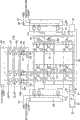
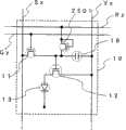
在图1中,在绝缘衬底20上设置了像素部分40、信号线驱动电路43、第一扫描线驱动电路41、第二扫描线驱动电路42以及监视电路64。In FIG. 1 , a
像素部分40设置有多个像素10,且每一个像素都设置有发光元件13以及连接到发光元件13并具有控制电流供应功能的晶体管(下文中称作驱动晶体管)12。发光元件13连接到以圆形所示的电源18。注意,在下面的实施方式中将举例说明像素10的具体结构。The
监视电路64包括监视发光元件66、连接到监视发光元件66的晶体管(下文中称作监视控制晶体管)111、以及其输出端子连接到监视控制晶体管的栅电极且其输入端子连接到监视控制晶体管的其中一个电极以及监视发光元件上的反相器112。恒流源105通过监视电流线(下文中称为监视线)113连接到监视控制晶体管111。监视控制晶体管111具有控制将电流从监视线113提供给多个监视发光元件66中的每一个的作用。由于监视线113通过晶体管连接到多个监视发光元件66所包括的电极上,该监视线可以具有监视电极电位的变化的功能。另外,恒流源105只要具有向监视线113提供恒定电流的功能即可。The
监视发光元件66和发光元件13在相同的条件下以相同的步骤来制造,从而也具有相同的结构。因此,它们对于环境温度的改变和随时间进展的退化具有相同或者几乎相同的特性。如上所述的监视发光元件66与以圆形所示的电源18相连接。在这里,连接到发光元件13的电源和连接到监视发光元件66的电源具有相等的电位,因此,用相同的附图标记电源18来表示它们。注意,在本实施方式中,假定监视控制晶体管111的极性为p沟道型来进行说明,然而,本发明并不限定于此,也可以采用n沟道型。在那种情况下,外围电路结构也需要适当地变化。The monitor light-emitting
不限制监视电路64的位置,并且可以在信号线驱动电路43和像素部分40之间,或者在第一扫描线驱动电路41或者第二扫描线驱动电路42和像素部分40之间设置监视电路64。The position of the
在监视电路64和像素部分40之间设置有缓冲放大器电路110。该缓冲放大器电路110具有两个输入端子,通过其中一个的输入端子连接到输出端子,可以具有相等的输入和输出电位。并且,该缓冲放大器电路是具有高输入阻抗以及高输出电流容量特性的电路。因此,只要是具有这些特性的电路,就可以适当地决定其电路结构。A
这种结构的缓冲放大器电路具有连同监视发光元件66的其中一个电极电位的变化,而改变施加到包含在像素部分40之内的发光元件13的电压的功能。The buffer amplifier circuit of this structure has a function of changing the voltage applied to the
在这种结构中,可以在相同的绝缘衬底20或者不同的衬底之上设置恒流源105和缓冲放大器电路110。In this structure, the constant
在前述结构中,从恒流源105向监视发光元件66提供恒定电流。当在这种状态下发生环境温度变化或者随时间的退化时,监视发光元件66的电阻值改变。例如,当发生随时间的退化时,监视发光元件66的电阻值增加。于是,由于提供给监视发光元件66的电流值是恒定的,所以在监视发光元件66的两端之间的电位差改变。具体地,在监视发光元件66的两个电极之间的电位差改变。此时,由于连接到电源18的电极电位被固定,所以连接到恒流源105的电极的电位改变。将该电极的电位变化通过监视线113提供给缓冲放大器电路110。In the foregoing structure, a constant current is supplied from the constant
换言之,将上述电极的电位变化输入给缓冲放大器电路110的输入端子。将从缓冲放大器电路110的输出端子输出的电位通过驱动晶体管12提供给发光元件13。具体地,被输出的电位作为发光元件13的一个电极的电位而提供。In other words, the potential change of the above electrodes is input to the input terminal of the
通过这样,将与环境温度的变化以及随时间的退化相关的在监视发光元件66中的变化反馈给发光元件13。其结果,发光元件13能够依照环境温度变化以及随时间的退化以某一亮度来发光。因此,能够提供一种发光器件,其能够免受环境温度变化以及随时间的退化的影响地来显示图像。By doing so, changes in the monitoring
此外,由于设置了多个监视发光元件66,其中的电位变化能够被平均化并提供给发光元件13。换言之,在本发明中,由于通过提供多个监视发光元件66而可以使电位变化平均化,所以这是优选的。Furthermore, since a plurality of monitor
通过提供多个监视发光元件66,可以做好对于其中发生短路等情况的监视发光元件的替换准备。By providing a plurality of monitor
此外,本发明可以设置连接到监视发光元件66的监视控制晶体管111和反相器112。这些元件是考虑到由于监视发光元件66中的缺陷(包括初始缺陷和随时间的缺陷)导致监视电路64的工作不良而提供的。例如,考虑如下情况:当恒流源105和监视控制晶体管111不通过其他晶体管等而连接在一起时,在多个监视发光元件中的某一个监视发光元件66由制作步骤中的不良等在该监视发光元件所包括的阳极和阴极之间导致短路。此时,来自恒流源105的电流通过监视线113更多地被提供到短路的监视发光元件66。由于多个监视发光元件互相并联连接,所以,当较多电流提供给短路的监视发光元件66时,所预定的一定量电流不提供给其他监视发光元件。结果,不能将监视发光元件66的适当的电位变化提供到发光元件13。Furthermore, the present invention may provide a
这种监视发光元件的短路是由于该监视发光元件的阳极电位和阴极电位相同或几乎相同而导致的。例如,在发光元件的制造过程中,因阳极和阴极之间的灰尘等可能引起短路。此外,除了阳极和阴极之间的短路,有可能由于扫描线和阳极之间发生短路,而在监视发光元件之内发生短路。Such a short circuit of the monitor light emitting element is caused by the fact that the potential of the anode and the cathode of the monitor light emitting element are the same or almost the same. For example, in the manufacturing process of a light-emitting element, a short circuit may be caused by dust or the like between the anode and the cathode. Furthermore, in addition to the short circuit between the anode and the cathode, there is a possibility that a short circuit occurs within the monitor light emitting element due to a short circuit between the scanning line and the anode.
鉴于上述问题,本发明提供了监视控制晶体管111和反相器112。监视控制晶体管111切断供应到短路的监视发光元件66的电流,就是说在电气上将短路的监视发光元件和监视线断开,以便防止上述那样的因监视发光元件66的短路等导致的过大电流的供应。In view of the above problems, the present invention provides the
反相器112具有当多个监视发光元件中的任何一个短路时,输出使监视控制晶体管关断的电位的功能。此外,反相器112具有当多个监视发光元件中没有任何一个短路时,输出使监视控制晶体管导通的电位的功能。The
将利用图5说明监视电路64的详细工作。如图5A所示,在监视发光元件66所包含的电极中,在假定阴极电极66c的电位低于阳极电极66a的电位时,阳极电极66a连接到反相器112的输入端子,并且阴极电极66c连接到电源18,从而具有固定电位。因此,当监视发光元件66所包含的阳极和阴极之间发生短路时,阳极电极66a的电位靠近阳极电极66c的电位。结果,由于将靠近阴极电极66c的电位的Low电位提供给反相器112,该反相器112所包含的p沟道型晶体管112p导通。于是,从反相器112输出p沟道型晶体管112p的高电位侧的电位(Va),并使其为监视控制晶体管111的栅极电位。换言之,输入到监视控制晶体管111的栅极的电位是Va,所以该监视控制晶体管111关断。The detailed operation of the
注意,用作Va的高电位侧的电位(High电位)的VDD被设定为与发光元件的阳极电极的电位(阳极电位)相同或更高。此外,n沟道型晶体管112n的低电位侧的电位、监视线113的Low电位以及Va的Low电位都可以具有相同的电位。一般来说,n沟道型晶体管112的低电位侧的电位是地电位。但是不局限于此,可以决定该n沟道型晶体管112n的低电位侧的电位,并使其对于High电位具有预定的电位差。预定的电位差可以根据发光材料的电流、电压、亮度特性或器件的规格来确定。Note that VDD serving as a potential (High potential) on the high potential side of Va is set to be the same as or higher than the potential (anode potential) of the anode electrode of the light emitting element. In addition, the potential on the low potential side of the n-channel transistor 112n, the Low potential of the
在此,应该注意的是在监视发光元件66中流过恒定电流的顺序。此时,需要在监视控制晶体管111导通的状态下,开始在监视线113中流过恒定电流。在本实施方式中,如图5B所示,将Va保持为Low,并且开始在监视线113中流过电流。而且,对于Va进行设定以便在监视线113的电位充分增加之后使该Va成为VDD。其结果,即使在监视控制晶体管111导通的情况下,也可以对监视线113进行充电。Here, attention should be paid to the order in which the constant current flows in the monitor
另一方面,当在监视发光元件66中没有短路时,由于阳极电极66a的电位被提供给反相器112,所以n沟道型晶体管112n导通。于是,从反相器112输出能够充分使晶体管111导通的电位或者地电位的低电位侧的电位,因此,监视控制晶体管111导通。On the other hand, when there is no short circuit in the monitor
根据上述结构,可以防止将来自恒流源105的电流提供到短路的监视发光元件66。从而,在存在有多个监视发光元件的情况下,当在监视发光元件中发生短路时,通过切断提供给短路的监视发光元件的电流,可以将监视线113的电位变化抑制到最小限度。其结果,可以将适当的监视发光元件66的电位变化提供到发光元件13。According to the above structure, it is possible to prevent the current from the constant
注意,在本实施方式中,恒流源105只要是能够提供恒定电流的电路就可以,例如,可以使用晶体管制作恒流源。例如,可以将工作于饱和区域的晶体管配置在每一个监视像素中,并通过调整其栅电极来调整流过像素的电流值。下文中,将说明其结构。Note that in this embodiment, the constant
在图20中,在绝缘衬底20上设置有像素部分40、信号线驱动电路43、第一扫描线驱动电路41、第二扫描线驱动电路42以及监视电路64。In FIG. 20 , a
像素部分40设置有多个像素10,且每一个像素都设置有发光元件13以及连接到发光元件13并具有控制电流供应功能的晶体管(下文中称作驱动晶体管)12。发光元件连接到以圆形所示的电源18。注意,在下面的实施方式中将举例说明像素10的具体结构。The
监视电路64包括监视发光元件66、连接到监视发光元件66的晶体管(下文中称作监视控制晶体管)111、连接到监视发光元件66的晶体管(下文中称作冗余晶体管)115、以及其输出端子连接到冗余晶体管的栅电极且其输入端子连接到监视控制晶体管的其中一个电极以及监视发光元件上的反相器112。缓冲放大器电路110通过取样线116连接到冗余晶体管115。电源117通过电源线118连接到监视控制晶体管111。此外,电压输出电路114通过控制线119连接到监视控制晶体管111的栅电极。监视控制晶体管111具有控制将电压从电源线118提供给多个监视发光元件66中的每一个的作用。由于电源线118连接到多个监视发光元件66所包括的电极上,所以电源线118具有监视该电极电位的变化的功能。另外,电源117只要具有向电源线118提供恒定电压的功能即可。The
监视发光元件66和发光元件13在相同的条件下以相同的步骤来制造,从而也具有相同的结构。因此,它们对于环境温度的改变和随时间进展的退化具有相同或者几乎相同的特性。如上所述的监视发光元件66与电源18相连接。在这里,连接到发光元件13的电源和连接到监视发光元件66的电源具有相等的电位,因此,用相同的参考标记电源18表示它们。注意,在本实施方式中,假定监视控制晶体管111的极性为p沟道型来进行说明,然而,本发明并不限定于此,也可以采用n沟道型。在那种情况下,外围电路结构也需要适当地变化。The monitor light-emitting
不限制监视电路64的位置,并且可以在信号线驱动电路43和像素部分40之间,或者在第一扫描线驱动电路41或者第二扫描线驱动电路42和像素部分40之间设置监视电路64。The position of the
在监视电路64和像素部分40之间设置有缓冲放大器电路110。该缓冲放大器电路是具有相等的输入和输出电位、高输入阻抗以及高输出电流容量特性的电路。因此,只要是具有这些特性的电路,就可以适当地决定其电路结构。A
电压输出电路114是指具有配合输入而输出任意电位的功能的电路,并且,不特别地限制其电路结构。例如,可以采用数字模拟转换电路等,其中通过输入视频信号等来确定输出电位。The voltage output circuit 114 refers to a circuit having a function of outputting an arbitrary potential in accordance with an input, and its circuit configuration is not particularly limited. For example, a digital-to-analog conversion circuit or the like may be employed in which an output potential is determined by inputting a video signal or the like.
在这样的结构中,缓冲放大器电路110具有连同监视发光元件66的其中一个电极电位的变化,而改变施加到包含在像素部分40之内的发光元件13的电压的功能。In such a structure, the
在这种结构中,可以在相同的绝缘衬底20或者不同的衬底之上设置缓冲放大器电路110和电压输出电路114。In this structure, the
在前述结构中,从电源117向监视发光元件66提供恒定电压。而且,通过工作于饱和区域的监视控制晶体管111将恒定电流提供给监视发光元件66。当在这种状态下发生环境温度变化或者随时间的退化时,监视发光元件66的电阻值改变。例如,当发生随时间的退化时,监视发光元件66的电阻值增加。于是,由于提供给监视发光元件66的电流值是恒定的,在监视发光元件66的电位差改变。具体地,在监视发光元件66的两个电极之间的电位差改变。此时,由于连接到以圆形所示的电源18的电极的电位被固定,连接到监视控制晶体管111的电极的电位改变。将该电极的电位变化通过冗余晶体管115和取样线116提供给缓冲放大器电路110。In the foregoing structure, a constant voltage is supplied from the power supply 117 to the monitor
换言之,将上述电极的电位变化输入给缓冲放大器电路110的输入端子。将从缓冲放大器电路110的输出端子输出的电位通过驱动晶体管12提供给发光元件13。具体地,被输出的电位作为发光元件13的一个电极的电位而提供。In other words, the potential change of the above electrodes is input to the input terminal of the
通过这样,将与环境温度的变化以及随时间的退化相关的在监视发光元件66中的改变反馈给发光元件13。其结果,发光元件13能够依照环境温度变化以及随时间的退化以某一亮度来发光。因此,能够提供一种发光器件,其能够免受环境温度变化以及随时间的退化的影响地来显示图像。By doing so, changes in the monitoring
此外,由于设置了多个监视发光元件66,其中的电位变化能够被平均化而提供给发光元件13。换言之,在本发明中,由于通过提供多个监视发光元件66可以使电位变化平均化,所以这是优选的。Furthermore, since a plurality of monitor light-emitting
通过提供多个监视发光元件66,可以做好对于其中发生短路等情况的监视发光元件的替换准备。By providing a plurality of monitor
鉴于上述问题,本发明提供了冗余晶体管和反相器112。冗余晶体管停止从短路的监视发光元件66取样,就是说,在电气上将短路的监视发光元件和缓冲放大器电路110断开,以便防止因如上所述的监视发光元件66的短路等导致的过大电流的供应。In view of the above problems, the present invention provides redundant transistors and
反相器112具有当多个监视发光元件66中的任何一个短路时,输出使冗余晶体管115关断的电位的功能。此外,反相器112具有当多个监视发光元件66中没有一个短路时,输出使冗余晶体管115导通的电位的功能。The
此外,尽管本实施方式中所描述的监视电路64包括多个监视发光元件66、监视控制晶体管111和反相器112,但本发明并不局限于此。例如,只要具有当监视发光元件短路时检测该情况,切断通过监视线113提供到短路的监视发光元件的电流的功能,就可以使用任何电路作为反相器112。具体地,反相器112只要具有使监视控制晶体管关断,以便切断提供到短路的监视发光元件的电流的功能即可。Furthermore, although the
此外,本实施方式中,使用多个监视发光元件66。由于即使监视发光元件中的某一个发生不良,也可以进行监视工作,所以这是优选的。而且,由于通过提供多个监视发光元件66可以使监视工作平均化,所以这是优选的。In addition, in this embodiment, a plurality of monitor
在本实施方式中,缓冲放大器电路110为了防止电位变动而设置。从而,除了该缓冲放大器电路110之外,还可以使用如缓冲放大器电路那样能够防止电位改动的其他电路。也就是说,在将监视发光元件66的一个电极电位传送到发光元件13的情况下,当监视发光元件66和发光元件13之间设置用于防止电位变动的电路时,该电路不局限于上述缓冲放大器电路110,可以使用具有任何结构的电路。In this embodiment, the
实施方式2
在本实施方式中,将说明与上述实施方式不同的,当监视发光元件短路时关断监视控制晶体管的电路结构以及其工作。In this embodiment mode, a circuit configuration for turning off a monitor control transistor when a monitor light-emitting element is short-circuited and its operation, which are different from the above-described embodiments, will be described.
图6A所示的监视电路64包括p沟道型的第一晶体管80、具有与第一晶体管共同的栅电极且与第一晶体管并联连接的n沟道型的第二晶体管81、与第二晶体管串联连接的n沟道型的第三晶体管82。监视发光元件66连接到第一和第二晶体管80、81的栅电极。监视控制晶体管111的栅电极连接到第一和第二晶体管80、81的互相连接的电极。其他结构与图5所示的监视电路64一样。The
另外,第一p沟道型晶体管80的高电位侧为电位Va,第三n沟道型晶体管82的栅电极电位为Vb。而且,使监视线113的电位、电位Va、电位Vb如图6B所示那样工作。In addition, the high potential side of the first p-
首先,在监视线113的电位充分地增加之后,使电位Va为High。在监视发光元件66短路的情况下,监视发光元件66的阳极电位,即点D的电位,降低到和监视发光元件66的阴极相同的程度。于是,Low电位被输入到第一和第二晶体管80、81的栅电极,从而n沟道型的第二晶体管81关断,p沟道型的第一晶体管80导通。而且,第一晶体管80的一个电位的高电位侧的电位被输入到监视控制晶体管111的栅电极,以使其关断。其结果,来自监视线113的电流不被供应到短路的监视发光元件66中。First, after the potential of the
此时,在因短路的范围小而使阳极电位略微降低的情形中,有可能难以控制第一和第二晶体管80、81中的任何一个为导通或关断。因此,如图6所示,将电位Vb供应到第三晶体管82的栅电极。也就是说,如图6B所示,当电位Va为High时,使电位Vb为Low电位。于是,n沟道型的第三晶体管82关断。其结果,在阳极电位为比Va降低第一晶体管的阀值电压的电位时,可以使第一晶体管80导通,而且可以使监视控制晶体管111关断。At this time, in the case where the anode potential is slightly lowered due to the small range of the short circuit, it may be difficult to control either of the first and
这样,通过控制电位Vb,即使在阳极电位略微降低时也可以正确地使监视控制晶体管111关断。In this manner, by controlling the potential Vb, the
注意,在监视发光元件正常工作时,监视控制晶体管111被控制为导通。也就是说,由于阳极电位与监视线113的High电位几乎相同,所以第二晶体管81导通。其结果,Low电位被施加到监视控制晶体管111的栅电极,从而监视控制晶体管111导通。Note that the
如图7A所示,监视电路64包括p沟道型的第一晶体管83、与第一晶体管串联连接的p沟道型的第二晶体管84、具有与第二晶体管共同的栅电极的n沟道型的第三晶体管85、具有与第一晶体管共同的栅电极且与第一晶体管并联连接的n沟道型的第四晶体管86。监视发光元件66连接到第二和第三晶体管84、85的栅电极。监视控制晶体管111的栅电极连接到第二和第三晶体管84、85的互相连接的电极。而且,监视控制晶体管111的栅电极连接到第四晶体管86的一个电极。其他结构与图5所示的监视电路64一样。As shown in FIG. 7A, the
首先,在监视线113的电位充分地增加之后,使电位Ve为Low,从而,第一晶体管83的栅电极电位变为Ve的Low电位。在监视发光元件66短路的情况下,监视发光元件66的阳极电位,即点D的电位,降低到和监视发光元件66的阴极相同的程度。于是,Low电位被输入到第二和第三晶体管84、85的栅电极,从而n沟道型的第三晶体管85关断,p沟道型的第二晶体管84导通。另外,当电位Ve为Low时,第一晶体管83导通,第四晶体管86关断。而且,第一晶体管83的高电位侧的电位Vf经由第二晶体管84被输入到监视控制晶体管111的栅电极,以使其关断。其结果,来自监视线113的电流不被供应到短路的监视发光元件66中。注意,High电位不断被提供到电位Vf。First, after the potential of the
这样,通过控制栅电极电位Ve,可以正确地使监视控制晶体管111关断。In this way, by controlling the gate electrode potential Ve, the
实施方式3
在本发明中,可以将反向电压施加到发光元件和监视发光元件。由此,本实施方式将说明施加反向电压的情况。In the present invention, a reverse voltage can be applied to the light emitting element and the monitor light emitting element. Therefore, this embodiment will describe the case where a reverse voltage is applied.
反向电压是指在以发光元件13和监视发光元件66发光时所施加的电压为正方向电压的情况下,施加反相正向电压的High电位和Low电位而得到的电压。如果用监视发光元件66具体地说明则是:为了反相阳极电极66a和阴极电极66c的电位,使施加到监视线113的电位低于电源18的电位。The reverse voltage refers to a voltage obtained by applying the High potential and the Low potential of the reverse forward voltage when the voltage applied when the
具体来说,如图16所示,阳极电极66a的电位(阳极电位:Va)和阴极电极66c的电位(阴极电位:Vc)为Low电位。与此同时,将监视线113的电位(V113)反相。这个阳极电位和阴极电位反相的期间称作反向电压施加周期。而且,在经过预定的反向电压施加周期后,返回阴极电位,并将恒定电流流过监视线113,以完成充电。也就是说,在充分地提高电压之后,返回电位。此时,监视线113的电位以曲线形返回,这是由于以恒定电流对多个监视发光元件充电,并且对寄生电容充电的缘故。Specifically, as shown in FIG. 16, the potential of the
优选的是,将阳极电位反相,接着将阴极电位反相。然后,在经过预定的反向电压施加周期后,返回阳极电位,接着返回阴极电位。然后,在将阳极电位反相的同时,将监视线113的电位充电到High。It is preferred to invert the anode potential followed by inversion of the cathode potential. Then, after a predetermined reverse voltage application period, the anode potential is returned, followed by the cathode potential. Then, while inverting the anode potential, the potential of the
在此反向电压施加周期中,驱动晶体管12和监视控制晶体管111需要变为导通。During this reverse voltage application period, the
对发光元件施加反向电压的结果是,能够改进发光元件13和监视发光元件66的缺陷状况,而提高可靠性。此外,发光元件13和监视发光元件66可能具有阳极和阴极短路的初始缺陷,这是由于异物的粘连、由阳极或阴极中的微小凸起产生的针孔、以及电致发光层的不均匀而导致的。当引起这些初始缺陷时,不能根据信号进行发光或者不发光,且大部分电流流过短路元件。其结果,引起图像不能良好地显示的问题。这种缺陷可能在任意像素中出现。As a result of applying a reverse voltage to the light-emitting element, it is possible to improve the defect status of the light-emitting
因此,如本实施方式所示,可以通过向发光元件13和监视发光元件66施加反向电压而使电流仅局部地流到短路部分,从而在短路部分中产生热,可以使其氧化或碳化。结果,可以使短路部分绝缘化,而且电流流到其他部分,就可以使发光元件13和监视发光元件66正确地工作。如此,即使存在初始缺陷,也可以通过上述那样地施加反向电压而消除该缺陷。注意,优选在发货之前进行这种短路部分的绝缘化。Therefore, as in this embodiment, by applying a reverse voltage to the light-emitting
另外,不仅是初始缺陷,而且还会产生随着时间的推移在阳极与阴极之间发生另一种短路。这种缺陷也称作累进缺陷。在此,如本发明中所示,通过定期向发光元件13和监视发光元件66施加反向电压,即使发生累进缺陷,也可以消除这种缺陷,因此,可以使发光元件13和监视发光元件66正确地工作。In addition, not only the initial defect, but also another short circuit that occurs over time between the anode and the cathode. Such defects are also called progressive defects. Here, as shown in the present invention, by periodically applying a reverse voltage to the light-emitting
另外,通过施加反向电压可以防止图像的烧印痕。该图像的烧印痕是由于发光元件13的退化状态而产生的,但通过施加反向电压可以降低退化程度。其结果,可以防止图像的烧印痕。In addition, image burn-in can be prevented by applying reverse voltage. The burnt mark of this image is generated due to the degraded state of the
一般来说,发光元件13和监视发光元件66的退化在初期进度很快,但随时间的推移其退化进度渐渐变慢。也就是说,退化过一次的发光元件13和监视发光元件66不容易产生程度更深的退化。其结果,在每个发光元件13之间发生不均匀。因此,可在发货之前,或在不显示画像时等,使所有发光元件13和监视发光元件66发光,从而使其中没有产生退化的元件产生退化,以使所有元件的退化状态平均化。也可以在发光器件中设置这样的使所有元件发光的结构。Generally, the degradation progress of the
实施方式4
在本实施方式中,将说明像素电路以及其结构的一个实例。In this embodiment mode, an example of a pixel circuit and its structure will be described.
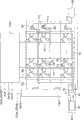
图2表示可以适用于本发明的像素部分的像素电路。在像素部分40中以矩阵形式提供有信号线Sx、扫描线Gy、电源线Vx,且每个交叉点上提供有像素10。该像素10包括开关晶体管11、驱动晶体管12、电容元件16、发光元件13。FIG. 2 shows a pixel circuit that can be applied to the pixel portion of the present invention. Signal lines Sx, scanning lines Gy, and power supply lines Vx are provided in a matrix form in the
说明在该像素中的连接关系。在信号线Sx和扫描线Gy的交叉处提供开关晶体管11。开关晶体管11的一个电极连接到信号线Sx而其栅电极连接到扫描线Gy。驱动晶体管12的一个电极连接到电源线Vx而其栅电极连接到开关晶体管11的另一电极。提供电容元件16以用于保持驱动晶体管12的栅源间的电压。在本实施方式中,电容元件16的一个电极连接到电源线Vx而其另一电极连接到驱动晶体管12的栅电极。注意,当例如驱动晶体管12的栅极电容大而漏电流小时就没有必要提供电容元件16。发光元件13连接到驱动晶体管12的另一电极。The connection relationship in this pixel is described. The switching
说明这种像素的驱动方法。A driving method of such a pixel will be described.
首先,当开关晶体管11导通时,从信号线Sx输入视频信号。按照视频信号在电容元件16中累积电荷。当在驱动晶体管12的栅源间的电压(Vgs)超出驱动晶体管12的阀值电压时,驱动晶体管12导通。于是,向发光元件13提供电流以发光。这时,驱动晶体管12在线性区或饱和区都可以工作。如果工作在饱和区,驱动晶体管12可以提供恒定电流。同时,如果工作在线性区,可以以恒定电压驱动驱动晶体管,使得功率消耗低。First, when the switching
下文中,参考定时图说明像素的驱动方法。Hereinafter, a driving method of a pixel is explained with reference to a timing chart.
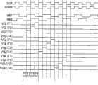
图8A是在每秒60次写图像的情况下的一个帧周期的定时图。在该定时图中,纵坐标表示扫描线G(从第一行到最后一行)而横坐标表示时间。FIG. 8A is a timing chart of one frame period in the case of writing an image 60 times per second. In this timing chart, the ordinate represents the scanning line G (from the first row to the last row) and the abscissa represents time.
一个帧周期包括m(m是2或更大的自然数)个子帧周期SF1、SF2、...、SFm,每个子帧周期SF1、SF2、...、SFm分别包括写入工作周期Ta1、Ta2、...、Tam、显示周期(发光周期)Ts1、Ts2、...、Tsm、反向电压施加周期和反向电位施加周期的预备周期SE。在本实施方式中,如图8A所示,一个帧周期提供有子帧周期SF1、SF2和SF3、反向电位施加周期的预备周期SE以及反向电压施加周期(FRB)。在每个子帧周期中,顺序进行写入工作周期Ta1到Ta3,各自后面跟着显示周期Ts1到Ts3。另外,只要能够显示分级,显示周期的长度就没有特别的限制。对在每秒写图像的次数也没有特别的限制。A frame period includes m (m is a natural number of 2 or more) subframe periods SF1, SF2, ..., SFm, and each subframe period SF1, SF2, ..., SFm includes writing duty periods Ta1, Ta2 , . . . , Tam, display period (emission period) Ts1, Ts2, . . . , Tsm, reverse voltage application period, and preliminary period SE of the reverse potential application period. In the present embodiment, as shown in FIG. 8A , one frame period is provided with subframe periods SF1 , SF2 , and SF3 , a preparation period SE of a reverse potential application period, and a reverse voltage application period (FRB). In each subframe period, writing duty periods Ta1 to Ta3 are sequentially performed, each followed by display periods Ts1 to Ts3. In addition, the length of the display period is not particularly limited as long as gradation can be displayed. There is also no particular limit to the number of times an image is written per second.
此外,不一定必须提供反向电压施加周期(FRB)。Also, it is not necessarily necessary to provide a reverse voltage application period (FRB).
也可以在一个帧周期中提供非发光周期。作为采用这个方式的效果之一可以举出当进行诸如动画显示时能够获得清晰图像。A non-light emitting period may also be provided in one frame period. As one of the effects of adopting this method, it is possible to obtain a clear image when performing, for example, animation display.
图8B的定时图示出某一行(第i行)的写入工作周期、显示周期和反向电压施加周期。在写入工作周期Ta1、Ta2、Ta3和显示周期Ts1、Ts2、Ts3交替出现之后出现反向电压施加周期RB。具有写入工作周期Ta1、Ta2、Ta3和显示周期Ts1、Ts2、Ts3的周期称作正向电压施加周期。The timing chart of FIG. 8B shows a writing duty period, a display period, and a reverse voltage application period of a certain row (i-th row). The reverse voltage application period RB occurs after the writing operation periods Ta1, Ta2, Ta3 and the display periods Ts1, Ts2, Ts3 appear alternately. A period having writing operation periods Ta1, Ta2, Ta3 and display periods Ts1, Ts2, Ts3 is called a forward voltage application period.
写入工作周期Ta可以分成多个工作周期。在本实施方式中,使其分成两个工作周期,其中一个进行删除工作,另一个进行写入工作。为了提供删除工作和写入工作,输入We(Write Erase)信号。在以下的实施方式将说明其他删除工作和写入工作以及信号的详细内容。The writing duty cycle Ta can be divided into multiple duty cycles. In this embodiment, it is divided into two work cycles, one of which performs deletion work, and the other performs write work. In order to provide delete work and write work, input We (Write Erase) signal. In the following embodiments, details of other delete operations, write operations, and signals will be described.
图21表示当将图8所示的一个帧周期的定时图的写入工作周期Ta分成四个工作周期时的一个具体例子。FIG. 21 shows a specific example when the writing duty cycle Ta in the timing chart of one frame cycle shown in FIG. 8 is divided into four duty cycles.
一个帧周期包括11个子帧周期而11个子帧周期包括10个显示周期和一个非发光周期。在本实施方式中,如图21所示,一个帧周期具有子帧周期,该子帧周期之一个成为非发光周期。另外,只要能够显示分级,就对显示周期的长度没有特别的限制。对在每秒写图像的次数也没有特别的限制。One frame period includes 11 subframe periods and the 11 subframe periods include 10 display periods and one non-emission period. In the present embodiment, as shown in FIG. 21 , one frame period has subframe periods, and one of the subframe periods is a non-emission period. In addition, as long as gradation can be displayed, there is no particular limitation on the length of the display period. There is also no particular limit to the number of times an image is written per second.
此外,可以提供多个非发光周期,也可以不提供。In addition, multiple non-light emitting periods may or may not be provided.
此外,写入工作周期Ta不仅可以分成删除工作和写入工作,还可以在一方进行写入工作,并在另一方也进行写入工作,亦即只进行多次写入工作。为了提供多个写入工作,输入WE(Write Erase)信号。当然,可以使用译码器电路。以下的实施方式将说明其详细内容。In addition, the writing operation cycle Ta can be divided into not only the deletion operation and the writing operation, but also the writing operation can be performed on one side and the writing operation can be performed on the other side, that is, only multiple writing operations can be performed. In order to provide multiple write jobs, input WE (Write Erase) signal. Of course, a decoder circuit can be used. The following embodiments will describe its details.
另外,在非发光周期中施加反向电压。直接在非发光周期之前提供使所有像素的开关晶体管同时导通的周期,亦即,使所有的扫描线导通的周期(导通周期)。In addition, a reverse voltage is applied during the non-emission period. A period in which switching transistors of all pixels are simultaneously turned on, that is, a period in which all scanning lines are turned on (conduction period) is provided immediately before the non-emission period.
在反向电压施加周期之后紧接着可以提供使所有像素的开关晶体管同时关断,即,使所有扫描线关断的周期(关断周期)。Immediately after the reverse voltage application period, a period for simultaneously turning off the switching transistors of all pixels, that is, turning off all scanning lines (off period) may be provided.
另外,紧接在反向电压施加周期之前提供删除周期(SE)。该删除周期可以进行与上述删除工作同样的工作。在删除周期中,按顺序删除紧接在删除周期之前的子帧周期,即在本实施方式中的SF3已写入的数据。这是因为,在导通周期,在完成最后一行的像素的显示周期之后开关晶体管同时导通,从而第一行等的像素具有不必要的显示周期。In addition, an erase period (SE) is provided immediately before the reverse voltage application period. This delete cycle can perform the same work as the delete work described above. In the erasure period, the subframe period immediately before the erasure period, that is, the data written in SF3 in this embodiment is deleted in order. This is because, in the turn-on period, the switching transistors are simultaneously turned on after the display period of the pixels of the last row is completed, so that the pixels of the first row and the like have an unnecessary display period.
如此,通过诸如扫描线驱动电路以及信号线驱动电路的驱动电路来进行为了提供导通周期、关断周期和删除周期的控制。In this way, control for providing an on period, an off period, and an erasing period is performed by a driving circuit such as a scanning line driving circuit and a signal line driving circuit.
注意,向发光元件13施加反向电压的时序,即反向电压施加周期并不限于图8A和8B所示的时序。那就是说,不一定对每个帧周期提供反向电压施加周期,也不一定在一个帧周期的后面部分中提供反向电压施加周期。只需要在紧接施加周期(RB)之前提供导通周期并且只需要在紧接施加周期(RB)之后提供关断周期。另外,反相发光元件的阳极电位和阴极电位的顺序并不限于图8A和8B所示的顺序。也就是说,在阴极电极的电位增加之后,阳极电极的电位可以下降。Note that the timing of applying the reverse voltage to the
图3示出图2中所示的像素电路的布局示例。首先,形成构成开关晶体管11和驱动晶体管12的半导体膜。然后,形成第一导电膜,并且用作栅绝缘膜的绝缘膜插在它们之间。该导电膜可以用作开关晶体管11和驱动晶体管12的栅电极以及扫描线Gy。这时,开关晶体管11优选有双栅结构。FIG. 3 shows an example of the layout of the pixel circuit shown in FIG. 2 . First, semiconductor films constituting the switching
然后,形成第二导电膜,并且用作层间绝缘膜的绝缘膜插在它们之间。该导电膜可以用作开关晶体管11和驱动晶体管12的漏极布线和源极布线,或可以用作信号线Sx和电源线Vx。这时,可以由堆叠第一导电膜、用作层间绝缘膜的绝缘膜以及第二导电膜的叠层结构来形成电容元件16。驱动晶体管12的栅电极通过接触孔连接到开关晶体管的另一电极。Then, a second conductive film is formed, and an insulating film serving as an interlayer insulating film is interposed therebetween. This conductive film can be used as the drain wiring and source wiring of the switching
提供在像素中的开口部分中形成像素电极19。该像素电极连接到驱动晶体管12的另一电极。如果在第二导电膜和像素电极19之间提供绝缘膜等,那么需要像素电极19通过接触孔连接到驱动晶体管12的另一电极。如果没有提供绝缘膜等,像素电极可以直接连接到驱动晶体管12的另一电极。A
图4是沿图3的线A-B和B-C切割获得的横截面视图。FIG. 4 is a cross-sectional view cut along lines A-B and B-C of FIG. 3 .
在绝缘衬底20上形成有被选择蚀刻的半导体膜,基底膜插在它们中间。作为绝缘衬底20,可以采用诸如钡硼硅酸盐玻璃和铝硼硅酸盐玻璃的玻璃衬底、石英衬底、不锈钢(SUS)衬底等。另外,由诸如以PET(聚对苯二甲酸乙二醇酯)、PEN(聚萘二甲酸乙二醇酯)以及PES(聚醚硫化物)为代表的塑料和丙烯酸的柔性合成树脂制成的衬底与其它衬底相比通常具有更低的热阻,但如其在制造步骤期间可以承受处理温度则可以使用它。作为基底膜,可以使用诸如氧化硅、氮化硅以及氮化氧化硅的绝缘膜。Selectively etched semiconductor films are formed on the insulating
在基底膜上形成具有25nm到100nm(优选为30nm到60nm)的厚度的非晶体半导体膜。除了硅之外,硅锗可以用于非晶体半导体膜。An amorphous semiconductor film having a thickness of 25 nm to 100 nm (preferably 30 nm to 60 nm) is formed on the base film. In addition to silicon, silicon germanium can be used for the amorphous semiconductor film.
接着,根据需求使非晶体半导体膜结晶,以形成晶体半导体膜。通过使用炉子、激光辐射、从灯发出的光的照射(此后称作灯退火)或者它们的组合可以进行结晶化。例如,通过向非晶体半导体膜掺杂金属元素并使用炉子进行热处理来形成晶体半导体膜。因为可以在低温下使半导体膜结晶,所以优选添加金属元素。Next, the amorphous semiconductor film is crystallized as necessary to form a crystalline semiconductor film. Crystallization may be performed by using a furnace, laser radiation, irradiation of light emitted from a lamp (hereinafter referred to as lamp annealing), or a combination thereof. For example, a crystalline semiconductor film is formed by doping an amorphous semiconductor film with a metal element and performing heat treatment using a furnace. Since a semiconductor film can be crystallized at a low temperature, it is preferable to add a metal element.
对这样形成的晶体半导体膜进行蚀刻以具有预定的形状。预定的形状是成为如在图3中所示的开关晶体管11和驱动晶体管12的形状。The crystalline semiconductor film thus formed is etched to have a predetermined shape. The predetermined shape is to be the shape of the switching
然后,形成用作栅绝缘膜的绝缘膜。形成厚度为10nm到150nm并且优选为20nm到40nm的该绝缘膜以便覆盖半导体膜。例如,绝缘膜可以使用氧化氮化硅膜、氧化硅膜等,并且可以采用单层结构或叠层结构。Then, an insulating film serving as a gate insulating film is formed. This insulating film is formed to have a thickness of 10 nm to 150 nm and preferably 20 nm to 40 nm so as to cover the semiconductor film. For example, a silicon oxide nitride film, a silicon oxide film, or the like can be used for the insulating film, and a single-layer structure or a stacked-layer structure can be adopted.
在半导体膜上形成用作栅电极的第一导电膜,栅绝缘膜插在它们中间。尽管栅电极可以具有单层结构或叠层结构,在本实施方式中使用由导电膜22a和22b构成的叠层结构。通过使用从Ta、W、Ti、Mo、Al和Cu中选择的元素或主要包含这种元素的合金材料或化合物材料可以形成每层导电膜22a和22b。在本实施方式中,导电膜22a由厚度为10nm到50nm,例如30nm的氮化钽膜制成,而导电膜22b堆叠在其上,使用的是厚度为200nm到400nm,例如370nm的钨膜。A first conductive film serving as a gate electrode is formed on the semiconductor film with a gate insulating film interposed therebetween. Although the gate electrode may have a single-layer structure or a stacked-layer structure, a stacked-layer structure composed of conductive films 22a and 22b is used in this embodiment mode. Each conductive film 22a and 22b can be formed by using an element selected from Ta, W, Ti, Mo, Al, and Cu, or an alloy material or a compound material mainly containing such an element. In this embodiment, the conductive film 22a is made of a tantalum nitride film with a thickness of 10nm to 50nm, such as 30nm, and the conductive film 22b is stacked thereon, using a tungsten film with a thickness of 200nm to 400nm, such as 370nm.
接着,以栅电极作为掩模添加杂质元素。这时,除高浓度杂质区外可以形成低浓度杂质区。这称作LDD(低掺杂漏极)结构。特别地,低浓度杂质区重叠于栅电极的结构称作GOLD(栅漏重叠的LDD)结构。N沟道型晶体管优选采用具有低浓度杂质区的结构。Next, an impurity element is added using the gate electrode as a mask. At this time, low-concentration impurity regions may be formed in addition to high-concentration impurity regions. This is called an LDD (Low Doped Drain) structure. In particular, a structure in which a low-concentration impurity region overlaps a gate electrode is called a GOLD (Gate-Drain Overlapped LDD) structure. An N-channel transistor preferably has a structure having a low-concentration impurity region.
该低浓度杂质区有可能引起不需要的电容的形成。因此,在使用具有LDD结构或GOLD结构的TFT来形成像素的情况下最好采用本发明的驱动方法。This low-concentration impurity region may cause unnecessary capacitance formation. Therefore, it is preferable to employ the driving method of the present invention when a pixel is formed using a TFT having an LDD structure or a GOLD structure.
随后,形成用作层间绝缘膜30的绝缘膜28和29。绝缘膜28可以由包含氮的绝缘膜形成,并且在本实施方式中,通过等离子体CVD形成厚度为100nm的氮化硅膜。此外,通过使用有机材料或无机材料可以形成绝缘膜29。有机材料包括聚酰亚胺、丙烯酸、聚酰胺、聚酰亚胺酰胺、苯并环丁烯、硅氧烷以及聚硅氮烷。硅氧烷由硅(Si)和氧(O)的结合物形成的骨架结构组成。硅氧烷以聚合物为起始材料来形成,该聚合物具有至少包含氢的有机组(诸如烷基群或芳烃)作为取代基、氟群作为取代基、或至少含氢的有机群和氟群之中的一种作为取代基。使用包含具有硅(Si)和氮(N)的结合物的聚合物材料的液体材料作为起始材料形成聚硅氮烷。无机材料包括含有氧或氮的绝缘膜,诸如氧化硅(SiOx)、氮化硅(SiNx)、氧化氮化硅(SiOxNy(x>y))以及氮化氧化硅(SiNxOy(x>y)(x,y=1,2...))。可选地,绝缘膜29可以具有这些绝缘膜的叠层结构。具体地,当通过使用有机材料形成绝缘膜29时,虽然改进了平整性而水分和氧被吸入有机材料中。为了阻止该情况,可以在有机材料上形成含有无机材料的绝缘膜。优选使用含氮的绝缘膜作为无机材料,因为可以防止诸如Na的碱离子进入。有机材料优选用于绝缘膜29,因为可以改进平整性。Subsequently, insulating
在层间绝缘膜30和栅绝缘膜中形成接触孔。然后,形成第二导电膜,其用作开关晶体管11和驱动晶体管12的源极布线和漏极布线24、信号线Sx以及电源线Vx。作为第二导电膜可以使用由诸如铝(Al)、钛(Ti)、钼(Mo)、钨(W)以及硅(Si)的元素构成的膜或者使用这些元素的合金膜。在本实施方式中,通过堆叠厚度分别为60nm、40nm、300nm和100nm的钛膜、氮化钛膜、铝硅合金膜以及钛膜(Ti、TiN、Al-Ti、Ti)形成第二导电膜。Contact holes are formed in the
然后,形成绝缘膜31以便覆盖第二导电膜。作为绝缘膜31可以使用上述的层间绝缘膜30的材料。通过提供这种绝缘膜31可以实现高的开口率。Then, an insulating
而且,在设在绝缘膜31的开口部分中形成像素电极(也称作第一电极)19。为了增加在开口部分中的像素电极的台阶覆盖性(stepcoverage),开口部分的末端部分优选是有多个曲率半径的稍圆的形状。作为像素电极19可以使用诸如铟锡氧化物(ITO)、通过将2%到20%的氧化锌(ZnO)混合到铟氧化物中获得的铟锌氧化物(IZO)、通过将2%到20%的氧化硅(SiO2)混合到氧化铟中获得的ITO-SiOx、有机铟以及有机锡的透光材料。像素电极19也可以使用从银(Ag)、钽、钨、钛、钼、铝以及铜中选择的元素或主要包含这种元素的合金材料或化合物材料的遮光材料。此时,当通过使用有机材料形成绝缘膜31以改进平整性时,像素电极的形成表面的平整性得以改进,从而可以施加恒定电压并防止短路。Also, a pixel electrode (also referred to as a first electrode) 19 is formed in an opening portion provided in the insulating
在第一导电膜重叠于像素电极的区域430中可能出现电容耦合。该电容耦合是不希望的电容。通过本发明的驱动方法可以去除这种不希望的电容。Capacitive coupling may occur in the
随后,通过汽相淀积或喷墨法形成电致发光层33。电致发光层33具有有机材料或无机材料,并任意组合电子注入层(EIL)、电子传输层(ETL)、发光层(EML)、空穴传输层(HTL)、空穴注入层(HIL)等来形成。注意,每层之间的界限不一定是清晰明确的,并且还有各层的材料彼此部分地混合的情况,这使得边界模糊。另外,电致发光层的结构并不限于上述叠层结构。Subsequently, the
而且,通过溅射或汽相淀积形成第二电极35。根据像素结构,发光元件的第一电极(像素电极)19和第二电极35用作阳极或阴极。Also, the
作为阳极材料优选使用具有高功函数(4.0eV或更高的功函数)的金属、合金、导电化合物以及其混合物等。更具体地,可以使用ITO、通过将2%到20%的氧化锌(ZnO)混合到氧化铟中获得的IZO、金(Au)、铂(Pt)、镍(Ni)、钨(W)、铬(Cr)、钼(Mo)、铁(Fe)、钴(Co)、铜(Cu)、钯(Pd)、金属材料的氮化物(TiN)等。Metals, alloys, conductive compounds, mixtures thereof, and the like having a high work function (work function of 4.0 eV or higher) are preferably used as the anode material. More specifically, ITO, IZO obtained by mixing 2% to 20% of zinc oxide (ZnO) into indium oxide, gold (Au), platinum (Pt), nickel (Ni), tungsten (W), Chromium (Cr), molybdenum (Mo), iron (Fe), cobalt (Co), copper (Cu), palladium (Pd), nitride (TiN) of metal materials, etc.
另一方面,作为阴极材料优选使用具有低功函数(3.8eV或更低的功函数)的金属、合金、导电化合物及其混合物。更具体地,可以使用属于周期表第一组或第二组的元素,即诸如Li和Cs的碱金属、诸如Mg、Ca和Sr的碱土金属、含它们的合金(Mg:Ag、Ai:Li)或化合物(LiF、CsF、CaF2)以及包括稀土金属的过渡金属。然而,因为需要阴极透光,所以将这些金属或包含它们的合金形成得极薄,并且堆叠诸如ITO的金属(包括合金)而形成。On the other hand, metals, alloys, conductive compounds, and mixtures thereof having a low work function (work function of 3.8 eV or less) are preferably used as the cathode material. More specifically, elements belonging to the first or second group of the periodic table, that is, alkali metals such as Li and Cs, alkaline earth metals such as Mg, Ca, and Sr, alloys containing them (Mg:Ag, Ai:Li ) or compounds (LiF, CsF, CaF2 ) and transition metals including rare earth metals. However, since cathode light transmission is required, these metals or alloys containing them are formed extremely thin, and metals (including alloys) such as ITO are stacked.
接下来,可以形成保护膜以覆盖第二电极35。作为保护膜,可以使用氮化硅膜或DLC膜。Next, a protective film may be formed to cover the
通过这种方式,可以完成发光器件的像素。In this way, a pixel of a light emitting device can be completed.
实施方式5
在本实施方式中,说明具有上述实施方式所示的像素电路的发光器件的整体结构,其中,写入周期Ta被分成两个工作周期,一个周期进行删除工作,另一个周期进行写入工作。In this embodiment, the overall structure of a light emitting device having the pixel circuit shown in the above embodiments is described, wherein the writing period Ta is divided into two working periods, one period is for erasing, and the other period is for writing.
如在图12中所示,本发明的发光器件包括以矩阵方式布置前面提到的多个像素10的像素部分40、第一扫描线驱动电路41、第二扫描线驱动电路42以及信号线驱动电路43。可以使第一扫描线驱动电路41和第二扫描线驱动电路42彼此面对地进行设置,并在二者之间插入像素部分40,或者可以在像素部分40的上下左右四个边中的一个边上设置第一扫描线驱动电路41和第二扫描线驱动电路42。As shown in FIG. 12, the light-emitting device of the present invention includes a
信号线驱动电路43包括脉冲输出电路44、锁存器45以及选择电路46。锁存器45具有第一锁存器47和第二锁存器48。选择电路46具有晶体管(此后称作TFT 49)和模拟开关50作为开关组件。在每列中提供对应于信号线的TFT 49和模拟开关50。另外,在本实施方式中,在每列中提供反相器51用于产生WE信号的反相信号。注意,当WE信号的反相信号由外部提供时,则不必提供反相器51。The signal
TFT 49的栅电极连接到选择信号线52,并且其一个电极连接到信号线而另一电极连接到电源53。在第二锁存器48和每条信号线之间提供模拟开关50。换言之,模拟开关50的输入端子连接到第二锁存器48而输出端子连接到信号线。模拟开关50的两个控制端子之一连接到选择信号线52而另一端子通过反相器51连接到选择信号线52。电源53具有关断每个像素中的驱动晶体管12的电位,并且如果n沟道型晶体管用作驱动晶体管12那么电源53的电位处于Low而如果p沟道型晶体管用作驱动晶体管12那么电源53的电位处于High。The gate electrode of the
第一扫描线驱动电路41包括脉冲输出电路54和选择电路55。第二扫描线驱动电路42包括脉冲输出电路56和选择电路57。分别向脉冲输出电路54和56输入启动脉冲(G1SP、G2SP)。还分别向脉冲输出电路54和56输入时钟脉冲(G1CK、G2CK)和其反相的时钟脉冲(G1CKB、G2CKB)。The first scanning
选择电路55和57连接到选择信号线52,但是包括在第二扫描线驱动电路42中的选择电路57通过反相器58连接到选择信号线52。换言之,通过选择信号线52输入到选择电路55和57的WE信号彼此反相。The
每个选择电路55和57分别包括三态缓冲电路。当从选择信号线52发送的信号处于High电平时三态缓冲电路进入工作状态,并且当信号处于Low电平时进入高阻抗状态。Each of the
包括在信号线驱动电路43中的脉冲输出电路44、包括在第一扫描线驱动电路41中的脉冲输出电路54以及包括在第二扫描线驱动电路42中的脉冲输出电路56包括由多个触发电路构成的移位寄存器或译码器电路。如果译码器电路用作脉冲输出电路44、54和56,那么可以随机选择信号线或扫描线。通过随机选择信号线或扫描线,可以防止当采用时间灰度方法时出现的伪轮廓。The
信号线驱动电路43的结构并不限于前面提到的结构,并且可以另外提供电平移动器或缓冲器。另外,第一扫描线驱动电路41和第二扫描线驱动电路42的结构也并不限于前面提到的结构,并且可以另外提供电平移动器或缓冲器。The structure of the signal
此外,在本发明中可以提供保护电路。保护电路可以包括多个电阻元件。例如,p沟道型晶体管可以用作多个电阻元件。可以在信号线驱动电路43、第一扫描线驱动电路41、或第二扫描线驱动电路42中提供保护电路,优选的是,在像素部分40和信号线驱动电路43、第一扫描线驱动电路41、或第二扫描线驱动电路42之间提供保护电路。这种保护电路可以防止元件由于静电而引起的退化或破坏。Furthermore, a protection circuit may be provided in the present invention. The protection circuit may include a plurality of resistive elements. For example, p-channel type transistors can be used as a plurality of resistance elements. A protection circuit may be provided in the signal
在本实施方式中,发光器件包括电源控制电路63。电源控制电路63具有用于向发光元件13供应电源的电源电路61和控制器62。电源电路61包括以圆形所示的第一电源17,该第一电源17通过驱动晶体管12和电源线Vx连接到发光元件13的像素电极。电源电路61还包括以圆形所示的第二电源18,该第二电源18通过连接到对面电极(counterelectrode)的电源线连接到发光元件13。In this embodiment, the light emitting device includes a
这种电源电路61,当向发光元件13施加正向电压使得发光元件13被提供有电流并发光时,设定第一电源17的电位高于第二电源18的电位。另一方面,当向发光元件13施加反向电压时,设定第一电源17的电位低于第二电源18的电位。可以通过从控制器62向电源电路61提供预定的信号来进行电源的这种设定。Such a
在本实施方式中,发光器件还包括监视电路64和控制电路65。控制电路65包括恒定电流源105和缓冲放大器电路110。监视电路64包括监视发光元件66、监视控制晶体管111以及反相器112。In this embodiment, the light emitting device further includes a
按照监测电路64的输出,控制电路65向电源控制电路63提供用于补正电源电位的信号。根据从控制电路65提供的信号,电源控制电路63补正提供给像素部分40的电源电位。The
具有上述结构的本发明的发光器件可以抑制由于环境温度的变化和随时间进展的退化而引起的电流值的变化,使得可靠性增加。而且,通过使用监视控制晶体管111和反相器112,可以防止来自恒流源105的电流流过短路的监视发光元件66中,从而可以将正确的电流值的变化提供到发光元件13。The light-emitting device of the present invention having the above structure can suppress changes in current value due to changes in ambient temperature and degradation over time, resulting in increased reliability. Furthermore, by using the
实施方式6Embodiment 6
本实施方式将参照附图说明具有上述结构的本发明的发光器件的工作过程。In this embodiment mode, the working process of the light emitting device of the present invention having the above structure will be described with reference to the accompanying drawings.
首先,将利用图14A描述信号线驱动电路43的工作过程。脉冲输出电路44被输入时钟信号(下文中称作SCK)、时钟反相信号(下文中称作SCKB)和启动脉冲(下文中称作SSP)。根据这些信号的时序,采样脉冲输出到第一锁存器47。输入有数据的第一列至最后列的第一锁存器47依据采样脉冲输入的时序来存储视频信号。当锁存脉冲输入时,存储在第一锁存器47中的视频信号同时传输到第二锁存器48。First, the operation of the signal
此处,描述在每个周期中选择电路46的工作过程,其中假设从选择信号线52传输的在L电平的WE信号的周期为T1,而从选择信号线52传输的在H电平的WE信号的周期为T2。周期T1和T2每个对应水平扫描周期的半个周期,将周期T1称为第一子栅极选择周期而将周期T2称为第二子栅极选择周期。Here, the operation process of the
在周期T1中(第一子栅极选择周期),从选择信号线52传送的WE信号是L电平,TFT 49导通而模拟开关50被关断。于是,多个信号线S1到Sn经设置在每列中的TFT 49电连接到电源53。即,多个信号线Sx具有与电源53相同的电位。这时,包括在被选择的像素10中的开关晶体管11被导通,电源53的电位经开关晶体管11传输到驱动晶体管12的栅电极。于是,驱动晶体管12被关闭,没有电流在发光元件13的两个电极之间流过,因此它就不发光。照此,不管输入到信号线Sx的视频信号如何,电源53的电位都被传输到驱动晶体管12的栅电极,其关闭开关晶体管11强制性地使发光元件13不发光,这种工作过程被称为删除工作。In the period T1 (the first sub-gate selection period), the WE signal transmitted from the
在周期T2中(第二子栅极选择周期),从选择信号线52传输的WE信号是H电平,TFT 49被关断而模拟开关50被导通。于是,存储在第二锁存器48的一行视频信号同时传输到每个信号线Sx。这时,像素10中的开关晶体管11被导通,视频信号经开关晶体管11传输到驱动晶体管12的栅电极。于是,根据输入的视频信号,驱动晶体管12被导通或关断,因此发光元件13的第一和第二电极具有不同的电位或相同的电位。特别是,当驱动晶体管12被导通时,发光元件13的第一和第二电极具有不同的电位,因此电流流入发光元件13。即,发光元件13发光。注意,流入发光元件13的电流与流动在驱动晶体管12的源漏间的电流相同。In the period T2 (second sub-gate selection period), the WE signal transmitted from the
另一方面,当驱动晶体管12被关闭时,发光元件13的第一和第二电极具有相同的电位,因此没有电流流入发光元件13。即,发光元件13不发光。如此,驱动晶体管12根据视频信号被导通或关闭,引起发光元件13的第一和第二电极具有不同电位或相同电位,这种工作过程被称为写入工作。On the other hand, when the driving
接下来,描述第一扫描线驱动电路41和第二扫描线驱动电路42的工作过程。脉冲输出电路54被输入G1CK、G1CKB和G1SP。根据这些信号的时序,脉冲顺序地输出到选择电路55。脉冲输出电路56被输入G2CK、G2CKB和G2SP。根据这些信号的时序,脉冲顺序地输出到选择电路57。图14B示出了给选择电路55和57的第i、j、k和p行(i、j、k和p是自然数,满足1≦i、j、k、p≦n)的每一行提供的脉冲电位。Next, the working process of the first scanning
在此,类似于信号线驱动电路43的工作过程的描述,描述每个周期内第一扫描线驱动电路41中的选择电路55和第二扫描线驱动电路42中的选择电路57的工作过程,其中假设从选择信号线52传输的在L电平的WE信号周期为T1,而从选择信号线52传送的在H电平的WE信号周期为T2。注意,图14B的定时图中,已接收来自第一扫描线驱动电路41的信号的栅极线Gy(y是自然数,满足1≦y≦n)的电位表示为VGy(41),而已接收来自第二扫描线驱动电路42的信号的栅极线的电位表示为VGy(42)。而且,VGy(41)和VGy(42)可以用相同的扫描线Gy而提供。Here, similar to the description of the working process of the signal
在周期T1中(第一子栅极选择周期),从选择信号线52传送的WE信号是L电平。于是,第一扫描线驱动电路41中的选择电路55被输入L电平的WE信号,因此选择电路55进入浮置状态。另一方面,第二扫描线驱动电路42中的选择电路57被输入通过使WE信号反相获得的H电平信号,因此选择电路57进入工作状态。即,选择电路57传输H电平信号(行选择信号)到第i行的栅极线Gi,因此栅极线Gi具有与H电平信号相同的电位。即,第i行的栅极线Gi被第二扫描线驱动电路42选择。结果,像素10中的开关晶体管11被导通。然后,信号线驱动电路43中的电源53的电位传输到驱动晶体管12的栅电极,因此驱动晶体管12被关闭,发光元件13的两个电极具有相同的电位。即,在此周期内,进行使发光元件13不发光的删除工作。In the period T1 (the first sub-gate selection period), the WE signal transmitted from the
在周期T2中(第二子栅极选择周期),从选择信号线52传送的WE信号是H电平。于是,第一扫描线驱动电路41中的选择电路55被输入H电平的WE信号,因此选择电路55处于工作状态。即,选择电路55传输H电平信号到第i行的栅极线Gi,因此栅极线Gi具有与H-电平信号相同的电位。即,第i行的栅极线Gi被第一扫描线驱动电路41选择。结果,像素10中的开关晶体管11被导通。然后,视频信号从信号线驱动电路43中的第二锁存器48传输到驱动晶体管12的栅电极,因此驱动晶体管12被导通或关闭,以及发光元件13的两个电极具有不同或相同的电位。即,在这个周期中,进行使发光元件13发光或不发光的写入工作。另一方面,第二扫描线驱动电路42中的选择电路57被输入L电平信号,因此它处于浮置状态。In the period T2 (the second sub-gate selection period), the WE signal transmitted from the
如此,栅极线Gy在周期T1(第一子栅极选择周期)中被第二扫描线驱动电路42选择,而在周期T2(第二子栅极选择周期)中被第一扫描线驱动电路41选择。即,第一扫描线驱动电路41和第二扫描线驱动电路42以互补的方式控制栅极线。另外,删除工作在第一子栅极选择周期和第二子栅极选择周期中的一个内进行,而写入工作在另一个内进行。In this way, the gate line Gy is selected by the second scanning
注意,在第i行的栅极线Gi被第一扫描线驱动电路41选择的周期内,第二扫描线驱动电路42不在工作状态(选择电路57处于浮置状态),或传输行选择信号到除第i行外的其它行的栅极线。同样,在第i行的栅极线Gi接收来自第二扫描线驱动电路42的行选择信号的周期内,第一扫描线驱动电路41处于浮置状态,或传输行选择信号到除第i行外的其它行的栅极线。Note that during the period when the gate line Gi of row i is selected by the first scanning
根据执行上述工作的本发明,能够将发光元件13强制关断,因此,可以提高占空比。另外,尽管发光元件13能被强制关断,也不需要设置用于释放电容元件16的电荷的TFT。这样,可以获得高孔径比。当获得高开口率时,发光元件的亮度随着发光区域的增加而减小。即,能够减小驱动电压以减小功耗。According to the present invention that performs the above-described operations, the
另外,在本实施方式中,需要将信号线驱动电路43的扫描周期设定为通常的两倍。为了解决该问题,可以提高信号线驱动电路43的SCK以及SCKB的频率,也可以将视频信号分成多个信号。In addition, in the present embodiment, it is necessary to set the scanning period of the signal
注意,本发明不限于上述将栅极选择周期分成两半的实施方式。栅极选择周期可以分成三个或更多的周期。Note that the present invention is not limited to the above-described embodiment in which the gate selection period is divided into two halves. The gate selection period can be divided into three or more periods.
实施方式7
在本实施方式中将说明可以应用上述驱动方法的像素结构。注意,省略与图2相同结构的说明。In this embodiment mode, a pixel structure to which the above driving method can be applied will be described. Note that the description of the same structure as that in FIG. 2 is omitted.
图9示出一种像素结构,其中,除了图2中示出的像素结构之外在电容元件16的两端提供第三晶体管25。第三晶体管25的功能是在预定周期内使累积在电容元件16中的电荷放电。该第三晶体管25也称作删除晶体管。由连接到第三晶体管25的栅电极的删除扫描线Ry控制预定周期。FIG. 9 shows a pixel structure in which a
图24示出一种像素结构,其中,除了图2中示出的像素结构之外提供删除二极管2401。删除二极管2401的功能是在预定周期内使累积在电容元件16中的电荷放电。该删除二极管2401的输出连接到驱动晶体管12的栅极。由连接到删除二极管2401的输入的删除扫描线Ry控制预定周期。FIG. 24 shows a pixel structure in which an erasing diode 2401 is provided in addition to the pixel structure shown in FIG. 2 . The function of the erasing diode 2401 is to discharge the charges accumulated in the
图25示出一种像素结构,其中,除了图2中示出的像素结构之外提供二极管接法的删除晶体管2501。删除晶体管2501的功能是在预定周期内使累积在电容元件16中的电荷放电。该删除晶体管2501的栅电极连接到删除扫描线Ry。由删除扫描线Ry控制预定周期。FIG. 25 shows a pixel structure in which a diode-connected erasure transistor 2501 is provided in addition to the pixel structure shown in FIG. 2 . The function of the erasing transistor 2501 is to discharge the charge accumulated in the
图26示出一种像素结构,其中,在图2中示出的像素结构中的Gy和Vx被两个像素共同使用,并每个Gy和Vx从Sx、Sx2输入数据信号,以图26的结构作为一个像素来实现面积灰度级。图26的发光元件2601和发光元件2602分别具有不同的发光面积,从而由发光面积可以显示灰度级。另外,可以和控制发光周期而显示灰度级的数字时分灰度级驱动方法相组合,也可以和根据数据信号的电位来控制驱动晶体管12的Vgs而显示灰度级的电压程序型模拟灰度级驱动方法相组合。FIG. 26 shows a pixel structure, wherein Gy and Vx in the pixel structure shown in FIG. The structure acts as a pixel to achieve area grayscale. The light emitting element 2601 and the light emitting element 2602 in FIG. 26 respectively have different light emitting areas, so gray scales can be displayed by the light emitting areas. In addition, it can be combined with a digital time-division gray-scale driving method that controls the light-emitting period to display gray levels, and can also be combined with a voltage-programmed analog gray-scale method that controls the Vgs of the
例如,在提供多个子帧周期的情况下,在短子帧周期期间由图9所示的第三晶体管25使电容元件16的电荷放电。其结果,可以提高占空比。For example, in the case of providing a plurality of subframe periods, the charge of the
图10A示出一种像素结构,其中,除了图2中示出的像素结构之外在驱动晶体管12和发光元件13之间提供第四晶体管36。第四晶体管36的栅电极连接到具有固定电位的第二电源线Vax。所以,可以无关于驱动晶体管12和第四晶体管36的栅源间的电压地向发光元件13提供恒定电流。该第四晶体管36也称作电流控制晶体管。FIG. 10A shows a pixel structure in which a
图10B示出不同于图10A的像素结构,不同之处在于,具有固定电位的第二电源线Vax与扫描线Gy被平行地提供。FIG. 10B shows a pixel structure different from FIG. 10A in that a second power supply line Vax having a fixed potential is provided in parallel with the scanning line Gy.
图10C示出不同于图10A和图10B的像素结构,不同之处在于,第四晶体管36的具有固定电位的栅电极连接到驱动晶体管12的栅电极。在如图10C中示出的不需要提供附加的电源线的像素结构中,可以维持开口率。FIG. 10C shows a pixel structure different from FIGS. 10A and 10B in that the gate electrode of the
图11示出一种像素结构,其中向图10A示出的像素结构添加图9示出的删除晶体管。删除晶体管可以使电容元件16的电荷放电。不用说,可以对图10B或10C示出的像素结构添加删除晶体管。FIG. 11 shows a pixel structure in which the deletion transistor shown in FIG. 9 is added to the pixel structure shown in FIG. 10A . Deleting the transistor allows the charge of the
那就是说,可以不受像素结构限制地应用本发明。That is to say, the present invention can be applied without being limited by the pixel structure.
实施方式8Embodiment 8
本实施方式中,将说明使用译码器电路的具有像素电路的发光器件的整体结构,其中,将实施方式4所示的写入周期Ta分成两个工作周期,其中一个进行写入工作,另一个也进行写入工作。In this embodiment mode, the overall structure of a light-emitting device with a pixel circuit using a decoder circuit will be described, wherein the writing period Ta shown in
如图13所描述,本发明的发光器件包括在实施方式4中所示的以矩阵方式布置多个像素10的像素部分40、译码器电路1341、信号线驱动电路1343。译码器电路优选在像素部分40的上下左右四个边中的一个边上设置。As described in FIG. 13 , the light emitting device of the present invention includes a
信号线驱动电路1343只要是能够同时将一行对应于视频信号(DATA)的电位(下文中称作线顺序驱动)输出到像素的电路就可以。例如,可举出图12所示的信号线驱动电路。The signal
译码器电路1341接收用于选择输出线的输入(SLN:Select LineNumber)。另外,译码器电路还接收时钟脉冲(GCK)和反相的时钟脉冲(GCKB)。The decoder circuit 1341 receives an input (SLN: Select LineNumber) for selecting an output line. In addition, the decoder circuit also receives a clock pulse (GCK) and an inverted clock pulse (GCKB).
译码器电路1341不一定需要是译码器电路。例如,可以使用移位寄存器。在此情况下,如实施方式5和实施方式6所示那样,当将写入周期分成N个时,需要N个扫描线驱动电路。The decoder circuit 1341 does not necessarily need to be a decoder circuit. For example, a shift register can be used. In this case, as shown in the fifth and sixth embodiments, when the write cycle is divided into N, N scanning line driving circuits are required.
另外,在本发明中可以提供保护电路。保护电路可以包括多个电阻元件。例如,p沟道型晶体管可以用作多个电阻元件。可以在信号线驱动电路1343或译码器电路1341中提供保护电路,优选的是,在像素部分40和信号线驱动电路1343或译码器电路1341之间提供保护电路。这种保护电路可以防止元件由于静电而引起的退化或破坏。In addition, a protection circuit may be provided in the present invention. The protection circuit may include a plurality of resistive elements. For example, p-channel type transistors can be used as a plurality of resistance elements. A protection circuit may be provided in the signal
在本实施方式中,发光器件包括电源控制电路63,电源控制电路63具有用于向发光元件13供应电源的电源电路61和控制器62。电源电路61包括以圆形所示的第一电源17,该第一电源17通过驱动晶体管12和电源线Vx连接到发光元件13的像素电极。电源电路61还包括以圆形所示的第二电源18,该第二电源18通过连接到对面电极的电源线连接到发光元件13。In this embodiment, the light emitting device includes a
这种电源电路61,当向发光元件13施加正向电压使得发光元件13被提供有电流并发光时,设定第一电源17的电位高于第二电源18的电位。另一方面,当向发光元件13施加反向电压时,设定第一电源17的电位低于第二电源18的电位。可以通过从控制器62向电源电路61提供预定的信号来进行电源的这种设定。Such a
在本实施方式中,发光器件还包括监测电路64和控制电路65。控制电路65包括恒定电流源105和缓冲放大器电路110。监测电路64包括监视发光元件66、监视控制晶体管111以及反相器112。In this embodiment, the light emitting device further includes a
按照监测电路64的输出,控制电路65向电源控制电路63提供用于补正电源电位的信号。根据从控制电路65提供的信号,电源控制电路63补正提供给像素部分40的电源电位。The
具有上述结构的本发明的发光器件可以抑制由于环境温度的变化和随时间进展的退化而引起的电流值的变化,使得可靠性增加。而且,通过使用监视控制晶体管111和反相器112,可以防止来自恒流源105的电流流过短路的监视发光元件66中,从而可以将正确的电流值的变化提供到发光元件13。The light-emitting device of the present invention having the above structure can suppress changes in current value due to changes in ambient temperature and degradation over time, resulting in increased reliability. Furthermore, by using the
实施方式9Embodiment 9
本实施方式将参照附图说明具有上述结构的本发明的发光器件的工作过程。In this embodiment mode, the working process of the light emitting device of the present invention having the above structure will be described with reference to the accompanying drawings.
首先,将利用图15A描述信号线驱动电路1343的工作过程。信号线驱动电路43被输入时钟信号(下文中称作SCK)、时钟反相信号(下文中称作SCKB)和启动脉冲(下文中称作SSP)。另外,信号线驱动电路1343可以使用已知的电路,只要能够实现图15A的电路构成就没有特别的限制。First, the operation of the signal
此处,在实施方式6中通过使用从选择信号线52传送的WE信号将写入期间分成为周期T1和周期T2,但本实施方式由于使用译码器电路1341,所以不需要是WE信号,而通过使用SLN信号可以与上述同样地将写入期间分成多个期间。另外,本实施方式将说明在一行选择周期中进行两次写入工作时的时序。此外,将每个写入工作分成为周期T1、周期T2,以及将周期T1称为第一子栅极选择周期而将周期T2称为第二子栅极选择周期。Here, in Embodiment 6, the writing period is divided into period T1 and period T2 by using the WE signal transmitted from the
在周期T1(第一子栅极选择周期)和周期T2(第二子栅极选择周期)中,输出对应于DATA信号的电位作为信号线驱动电路1343的输出。这时,像素10中的开关晶体管11被导通,视频信号经开关晶体管11传输到驱动晶体管12的栅电极。于是,根据输入的视频信号,驱动晶体管12被导通或关断,因此发光元件13的第一和第二电极具有不同的电位,电流流入发光元件13。即,发光元件13发光。注意,流入发光元件13的电流与流动在驱动晶体管12的源漏间的电流相同。In a period T1 (first sub-gate selection period) and a period T2 (second sub-gate selection period), a potential corresponding to the DATA signal is output as an output of the signal
另一方面,当驱动晶体管12被关闭时,发光元件13的第一和第二电极具有相同的电位,因此没有电流流入发光元件13。即,发光元件13不发光。如此,驱动晶体管12根据视频信号被导通或关闭,引起发光元件13的第一和第二电极具有不同电位或相同电位,这种工作过程被称为写入工作。On the other hand, when the driving
接下来,描述译码器电路1341的工作过程。译码器电路1341被输入GCK、GCKB和SLN。SLN选择从译码器电路1431输出的行。图15B示出了给栅极线Gy的第i、j、k和p行(i、j、k和p是自然数,满足1≦i、j、k、p≦n)的每一行提供的脉冲电位。图15B示出了给选择电路55和57的第i、j、k和p行(i、j、k和p是自然数,满足1≦i、j、k、p≦n)的每一行提供的脉冲电位。Next, the operation of the decoder circuit 1341 will be described. The decoder circuit 1341 is input with GCK, GCKB, and SLN. The SLN selects the row output from the decoder circuit 1431 . Fig. 15B shows the pulses provided to each row of the i, j, k and p rows (i, j, k and p are natural numbers satisfying 1≦i, j, k, p≦n) of the gate line Gy potential. Fig. 15B shows the i, j, k and p rows (i, j, k and p are natural numbers satisfying 1≦i, j, k, p≦n) provided to each row of the
在此,类似于信号线驱动电路1343的工作过程的描述,可以分成为周期T1和周期T2。注意,图15B的定时图中,将在周期T1中来自译码器电路1341的栅极线Gy(y是自然数,满足1≦y≦n)的电位表示为VGy(T1),而将在周期T2中来自译码器电路1341的栅极线Gy的电位表示为VGy(T2)。而且,VGy(T1)和VGy(T2)可以用相同的扫描线Gy而提供。另外,在周期T1和周期T2分别对栅极线Gy进行扫描。Here, similar to the description of the working process of the signal
在周期T1中(第一子栅极选择周期),译码器电路1341传输H电平信号(行选择信号)到第i行的栅极线Gi,因此栅极线Gi具有与H电平信号相同的电位。即,第i行的栅极线Gi被译码器电路1341选择。结果,像素10中的开关晶体管11被导通。然后,信号线驱动电路1343中的电源53的电位传输到驱动晶体管12的栅电极,因此驱动晶体管12被导通或关闭,以及发光元件13的两个电极具有不同或相同的电位。即,在这个周期中,进行使发光元件13发光或不发光的写入工作。In the period T1 (the first sub-gate selection period), the decoder circuit 1341 transmits an H-level signal (row selection signal) to the gate line Gi of the i-th row, so the gate line Gi has the same signal as the H-level signal. same potential. That is, the gate line Gi of the i-th row is selected by the decoder circuit 1341 . As a result, the switching
在周期T2中(第二子栅极选择周期),译码器电路1341传输H电平信号(行选择信号)到第i行的栅极线Gi,因此栅极线Gi具有与H电平信号相同的电位。即,第i行的栅极线Gi被译码器电路1341选择。结果,像素10中的开关晶体管11被导通。然后,信号线驱动电路1343中的电源53的电位传输到驱动晶体管12的栅电极,因此驱动晶体管12被导通或关闭,以及发光元件13的两个电极具有不同或相同的电位。即,在这个周期中,进行使发光元件13发光或不发光的写入工作。In the period T2 (the second sub-gate selection period), the decoder circuit 1341 transmits an H-level signal (row selection signal) to the gate line Gi of the i-th row, so the gate line Gi has the same signal as the H-level signal. same potential. That is, the gate line Gi of the i-th row is selected by the decoder circuit 1341 . As a result, the switching
如此,栅极线Gy在周期T1(第一子栅极选择周期)中被译码器电路1341选择,而在周期T2(第二子栅极选择周期)中被译码器电路1341选择另外一行。即,在第一子栅极选择周期和第二子栅极选择周期中的一个内进行写入工作,而在另一个内也进行写入工作。In this way, the gate line Gy is selected by the decoder circuit 1341 in the period T1 (the first sub-gate selection period), and another row is selected by the decoder circuit 1341 in the period T2 (the second sub-gate selection period). . That is, the writing operation is performed in one of the first sub-gate selection period and the second sub-gate selection period, and the writing operation is also performed in the other.
也就是说,本发明的信号线驱动电路1343可以在写入周期中进行两次工作,而分别将信号输出到在周期T1和周期T2中所分别选择的栅极线Gy。That is to say, the signal
另外,在本实施方式中,需要将信号线驱动电路1343的扫描周期设定为通常的两倍。为了解决该问题,可以提高信号线驱动电路1343的SCK以及SCKB的频率,也可以将视频信号分成多个信号。In addition, in the present embodiment, it is necessary to set the scanning period of the signal
注意,本发明不限于上述将栅极选择周期分成两半的实施方式。栅极选择周期可以分成3个或更多的周期。另外,被分割的栅极选择周期可以用写入工作、删除工作任意组合。例如,可以将栅极选择周期分成为3个,其中两次进行写入工作而一次进行删除工作。Note that the present invention is not limited to the above-described embodiment in which the gate selection period is divided into two halves. The gate selection period can be divided into 3 or more periods. In addition, the divided gate selection period can be arbitrarily combined with writing operation and erasing operation. For example, the gate selection period can be divided into three, and writing operation is performed twice and erasing operation is performed once.
实施方式10
本实施方式中,将说明一种具有像素电路的发光器件的整体结构,其中,将以下的,即,将在实施方式4中描述的写入周期Ta分成为两个工作周期,在其中一个工作周期中进行写入工作,并在另一个工作周期中也进行写入工作的具有像素电路的发光器件的整体结构,使用移位寄存器,将写入周期Ta分成为4个工作周期,并在所有工作周期中进行写入工作。In this embodiment mode, an overall structure of a light-emitting device having a pixel circuit will be described, in which the following, that is, the writing period Ta described in
如图18所描述,本发明的发光器件包括在实施方式4中所示的以矩阵方式布置多个像素10的像素部分40、第一扫描线驱动电路1839、第二扫描线驱动电路1840、第三扫描线驱动电路1841、第四扫描线驱动电路1842、以及信号线驱动电路1843。第一扫描线驱动电路1839、第二扫描线驱动电路1840、第三扫描线驱动电路1841、第四扫描线驱动电路1842优选设置为彼此面对且一侧设置两个,并具有插入其间的像素部分40,或者优选在像素部分40的上下左右四个边中的一个边上设置。或者,也可以不是一侧设置两个,而是分为一侧一个和3个等,对布置的位置没有特别限制。As described in FIG. 18 , the light emitting device of the present invention includes a
信号线驱动电路1843只要是能够同时将对应于视频信号(DATA)的电位输出到整个行(下文中称作线顺序驱动)的电路就可以。例如,可举出图12所示的信号线驱动电路。The signal line driving circuit 1843 may be any circuit as long as it can output the potential corresponding to the video signal (DATA) to the entire row at the same time (hereinafter referred to as line sequential driving). For example, the signal line driver circuit shown in FIG. 12 can be mentioned.
分别向第一扫描线驱动电路1839、第二扫描线驱动电路1840、第三扫描线驱动电路1841、第四扫描线驱动电路1842输入启动脉冲(G1SP、G2SP、G3SP、G4SP)、时钟脉冲(G1CK、G2CK、G3CK、G4CK)和其反相的时钟脉冲(G1CKB、G2CKB、G3CKB、G4CKB)、WE1信号、以及WE2信号。Start pulses (G1SP, G2SP, G3SP, G4SP) and clock pulses (G1CK) are input to the first scanning line driving circuit 1839, the second scanning line driving circuit 1840, the third scanning line driving circuit 1841, and the fourth scanning line driving circuit 1842, respectively. , G2CK, G3CK, G4CK) and its inverted clock pulses (G1CKB, G2CKB, G3CKB, G4CKB), WE1 signal, and WE2 signal.
此外,在本发明中可以提供保护电路。保护电路可以包括多个电阻元件。例如,p沟道型晶体管可以用作多个电阻元件。可以分别在信号线驱动电路1843、第一扫描线驱动电路1839、第二扫描线驱动电路1840、第三扫描线驱动电路1841、第四扫描线驱动电路1842中提供保护电路,优选的是,在像素部分40和信号线驱动电路43、第一扫描线驱动电路1839、第二扫描线驱动电路1840、第扫三描线驱动电路1841或第四扫描线驱动电路1842之间提供保护电路。这种保护电路可以防止元件由于静电而引起的退化或破坏。Furthermore, a protection circuit may be provided in the present invention. The protection circuit may include a plurality of resistive elements. For example, p-channel type transistors can be used as a plurality of resistance elements. Protection circuits can be provided in the signal line driver circuit 1843, the first scan line driver circuit 1839, the second scan line driver circuit 1840, the third scan line driver circuit 1841, and the fourth scan line driver circuit 1842, preferably in A protection circuit is provided between the
在本实施方式中,发光器件包括电源控制电路63。电源控制电路63具有用于向发光元件13供应电源的电源电路61和控制器62。电源电路61包括以圆形所示的第一电源17,该第一电源17通过驱动晶体管12和电源线Vx连接到发光元件13的像素电极。另外,电源电路61还包括以圆形所示的第二电源18,该第二电源18通过连接到对面电极(counterelectrode)的电源线连接到发光元件13。In this embodiment, the light emitting device includes a
这种电源电路61,当向发光元件13施加正向电压使得发光元件13被提供有电流并发光时,设定第一电源17的电位高于第二电源18的电位。另一方面,当向发光元件13施加反向电压时,设定第一电源17的电位低于第二电源18的电位。可以通过从控制器62向电源电路61提供预定的信号来进行电源的这种设定。Such a
在本实施方式中,发光器件还包括监测电路64和控制电路65。控制电路65包括恒定电流源105和缓冲放大器电路110。监测电路64包括监视发光元件66、监视控制晶体管111以及反相器112。In this embodiment, the light emitting device further includes a
按照监测电路64的输出,控制电路65向电源控制电路63提供用于补正电源电位的信号。根据从控制电路65提供的信号,电源控制电路63补正提供给像素部分40的电源电位。The
具有上述结构的本发明的发光器件可以抑制由于环境温度的变化和随时间进展的退化而引起的电流值的变化,使得可靠性增加。而且,通过使用监视控制晶体管111和反相器112,可以防止来自恒流源105的电流流过短路的监视发光元件66中,从而可以将正确的电流值的变化提供到发光元件13。The light-emitting device of the present invention having the above structure can suppress changes in current value due to changes in ambient temperature and degradation over time, resulting in increased reliability. Furthermore, by using the
实施方式11
本实施方式将参照附图说明具有上述结构的本发明的发光器件的工作过程。In this embodiment mode, the working process of the light emitting device of the present invention having the above structure will be described with reference to the accompanying drawings.
首先,将利用图19A描述信号线驱动电路1843的工作过程。信号线驱动电路1843被输入时钟信号(下文中称作SCK)、时钟反相信号(下文中称作SCKB)和启动脉冲(下文中称作SSP)。另外,信号线驱动电路1343可以使用已知的电路,只要是能够实现图15A的电路构成就没有特别的限制。First, the operation of the signal line driver circuit 1843 will be described using FIG. 19A. The signal line driver circuit 1843 is input with a clock signal (hereinafter referred to as SCK), a clock inversion signal (hereinafter referred to as SCKB), and a start pulse (hereinafter referred to as SSP). In addition, a known circuit can be used for the signal
此处,在实施方式6中通过使用从选择信号线52传送的WE信号将写入期间分成为周期T1和周期T2,但本实施方式由于不进行删除工作,所以WE1信号和WE2信号不输入到信号线驱动电路1843。另外,本实施方式将说明在一行选择周期中进行4次写入工作时的时序。此外,将每个写入工作分成为周期T1、周期T2、周期T3、周期T4,以及将周期T1称为第一子栅极选择周期,将周期T2称为第二子栅极选择周期,将周期T3称为第三子栅极选择周期,将周期T4称为第四子栅极选择周期。Here, in Embodiment 6, the write period is divided into cycle T1 and cycle T2 by using the WE signal transmitted from the
在周期T1(第一子栅极选择周期)、周期T2(第二子栅极选择周期)、周期T3(第三子栅极选择周期)和周期T4(第四子栅极选择周期)中,输出对应于DATA信号的电位作为信号线驱动电路1843的输出。这时,像素10中的开关晶体管11被导通,视频信号经开关晶体管11传输到驱动晶体管12的栅电极。于是,根据输入的视频信号,驱动晶体管12被导通或关断,因此发光元件13的第一和第二电极具有不同的电位,电流流入发光元件13。即,发光元件13发光。注意,流入发光元件13的电流与流动在驱动晶体管12的源漏间的电流相同。In period T1 (first sub-gate selection period), period T2 (second sub-gate selection period), period T3 (third sub-gate selection period) and period T4 (fourth sub-gate selection period), A potential corresponding to the DATA signal is output as an output of the signal line driver circuit 1843 . At this time, the switching
另一方面,当驱动晶体管12被关闭时,发光元件13的第一和第二电极具有相同的电位,因此没有电流流入发光元件13。即,发光元件13不发光。如此,驱动晶体管12根据视频信号被导通或关闭,引起发光元件13的第一和第二电极具有不同电位或相同电位,这种工作过程被称为写入工作。On the other hand, when the driving
接下来,描述第一扫描线驱动电路1839、第二扫描线驱动电路1840、第三扫描线驱动电路1841和第四扫描线驱动电路1842的工作过程。第一扫描线驱动电路1839被输入GCK、GCKB、G1SP、WE1和WE2。根据GCK、GCKB、G1SP顺序地执行扫描,并根据WE1和WE2,顺序地决定是否将信号输出到栅极线Gy。第二扫描线驱动电路1840被输入GCK、GCKB、G2SP、WE1和WE2。根据GCK、GCKB、G2SP顺序地执行扫描,并根据WE1和WE2,顺序地决定是否将信号输出到栅极线Gy。第三扫描线驱动电路1841被输入GCK、GCKB、G3SP、WE1和WE2。根据GCK、GCKB、G3SP顺序地执行扫描,并根据WE1和WE2,顺序地决定是否将信号输出到栅极线Gy。第四扫描线驱动电路1842被输入GCK、GCKB、G4SP、WE1和WE2。根据GCK、GCKB、G4SP顺序地执行扫描,并根据WE1和WE2,顺序地决定是否将信号输出到栅极线Gy。图19B示出了给栅极线Gy的第i、j、k和p行(i、j、k和p是自然数,满足1≦i、j、k、p≦n)的每一行提供的脉冲电位。而且,图19B示出了给选择电路55和57的第i、j、k和p行(i、j、k和p是自然数,满足1≦i、j、k、p≦n)的每一行提供的脉冲电位。Next, the working process of the first scanning line driving circuit 1839 , the second scanning line driving circuit 1840 , the third scanning line driving circuit 1841 and the fourth scanning line driving circuit 1842 will be described. The first scanning line driving circuit 1839 is inputted with GCK, GCKB, G1SP, WE1, and WE2. Scanning is sequentially performed based on GCK, GCKB, G1SP, and whether to output a signal to the gate line Gy is sequentially determined based on WE1 and WE2. The second scan line driving circuit 1840 is inputted with GCK, GCKB, G2SP, WE1 and WE2. Scanning is sequentially performed based on GCK, GCKB, and G2SP, and whether to output a signal to the gate line Gy is sequentially determined based on WE1 and WE2. The third scanning line driving circuit 1841 is inputted with GCK, GCKB, G3SP, WE1 and WE2. Scanning is sequentially performed based on GCK, GCKB, G3SP, and whether to output a signal to the gate line Gy is sequentially determined based on WE1 and WE2. The fourth scanning line driving circuit 1842 is inputted with GCK, GCKB, G4SP, WE1 and WE2. Scanning is sequentially performed based on GCK, GCKB, G4SP, and whether to output a signal to the gate line Gy is sequentially determined based on WE1 and WE2. Fig. 19B shows the pulses provided to each row of the i, j, k and p rows (i, j, k and p are natural numbers satisfying 1≦i, j, k, p≦n) of the gate line Gy potential. Moreover, FIG. 19B shows each row of the i, j, k and p rows (i, j, k and p are natural numbers satisfying 1≦i, j, k, p≦n) for the
在此,类似于信号线驱动电路1843的工作过程的描述,可以分成为周期T1、周期T2、周期T3和周期T4。在此,将描述每个周期内的第一扫描线驱动电路1839、第二扫描线驱动电路1840、第三扫描线驱动电路1841、第四扫描线驱动电路1842的工作过程,其中,假设在WE1信号为L电平且WE2信号为L电平的周期为T1,在WE1信号为H电平且WE2信号为L电平的周期为T2,在WE1信号为H电平且WE2信号为H电平的周期为T3,在WE1信号为L电平且WE2信号为H电平的周期为T4。在图19B的定时图中,将已接收来自第一扫描线驱动电路1839的信号的栅极线Gy(y是自然数,满足1≦y≦n)的电位表示为Vgy(T1),已接收来自第二扫描线驱动电路1840的信号的栅极线Gy(y是自然数,满足1≦y≦n)的电位表示为Vgy(T2),已接收来自第三扫描线驱动电路1841的信号的栅极线Gy(y是自然数,满足1≦y≦n)的电位表示为Vgy(T3),已接收来自第四扫描线驱动电路1842的信号的栅极线Gy(y是自然数,满足1≦y≦n)的电位表示为VGy(T4)。而且,VGy(T1)、VGy(T2)、VGy(T3)和VGy(T4)可以用相同的扫描线Gy而提供。Here, similar to the description of the working process of the signal line driving circuit 1843, it can be divided into period T1, period T2, period T3 and period T4. Here, the working process of the first scanning line driving circuit 1839, the second scanning line driving circuit 1840, the third scanning line driving circuit 1841, and the fourth scanning line driving circuit 1842 in each cycle will be described. The period when the signal is L level and the WE2 signal is L level is T1, the period when the WE1 signal is H level and the WE2 signal is L level is T2, and the period when the WE1 signal is H level and the WE2 signal is H level The cycle of WE1 is T3, and the cycle when the WE1 signal is at the L level and the WE2 signal is at the H level is T4. In the timing diagram of FIG. 19B, the potential of the gate line Gy (y is a natural number, satisfying 1≦y≦n) that has received the signal from the first scanning line driving circuit 1839 is expressed as Vgy(T1). The potential of the gate line Gy (y is a natural number, satisfying 1≦y≦n) of the signal of the second scanning line driving circuit 1840 is expressed as Vgy (T2), and the gate that has received the signal from the third scanning line driving circuit 1841 The potential of the line Gy (y is a natural number, satisfying 1≦y≦n) is expressed as Vgy (T3), and the gate line Gy (y is a natural number, satisfying 1≦y≦n) having received the signal from the fourth scanning line driving circuit 1842 The potential of n) is expressed as VGy(T4). Also, VGy(T1), VGy(T2), VGy(T3) and VGy(T4) can be provided with the same scan line Gy.
在周期T1中(第一子栅极选择周期),WE1信号是L电平,WE2信号是L电平。于是,第二扫描线驱动电路1840、第三扫描线驱动电路1841、第四扫描线驱动电路1842被输入L电平的WE1信号和L电平的WE2信号,因此第二扫描线驱动电路1840、第三扫描线驱动电路1841、第四扫描线驱动电路1842进入浮置状态。另一方面,第一扫描线驱动电路1839也被输入L电平的WE1信号和L电平的WE2信号,第一扫描线驱动电路1839传输H电平信号到第i行的栅极线Gi,因此栅极线Gi具有与H电平信号相同的电位。即,第i行的栅极线Gi被第一扫描线驱动电路1839选择。结果,像素10中的开关晶体管11被导通。然后,信号线驱动电路1843中的电源53的电位传输到驱动晶体管12的栅电极,因此驱动晶体管12被导通或关闭,以及发光元件13的两个电极具有不同或相同的电位。即,在这个周期中,进行使发光元件13发光或不发光的写入工作。In the period T1 (the first sub-gate selection period), the WE1 signal is at L level, and the WE2 signal is at L level. Then, the second scanning line driving circuit 1840, the third scanning line driving circuit 1841, and the fourth scanning line driving circuit 1842 are input with the L-level WE1 signal and the L-level WE2 signal, so the second scanning line driving circuit 1840, The third scanning line driving circuit 1841 and the fourth scanning line driving circuit 1842 enter a floating state. On the other hand, the first scanning line driving circuit 1839 is also input with an L-level WE1 signal and an L-level WE2 signal, and the first scanning line driving circuit 1839 transmits an H-level signal to the gate line Gi of the i-th row, Therefore, the gate line Gi has the same potential as the H level signal. That is, the gate line Gi in the i-th row is selected by the first scanning line driving circuit 1839 . As a result, the switching
在周期T2中(第二子栅极选择周期),WE1信号是H电平,WE2信号是L电平。于是,第一扫描线驱动电路1839、第三扫描线驱动电路1841、第四扫描线驱动电路1842被输入H电平的WE1信号和L电平的WE2信号,因此第一扫描线驱动电路1839、第三扫描线驱动电路1841、第四扫描线驱动电路1842进入浮置状态。另一方面,第二扫描线驱动电路1840也被输入H电平的WE1信号和L电平的WE2信号,第二扫描线驱动电路1840传输H电平信号到第i行的栅极线Gi,因此栅极线Gi具有与H电平信号相同的电位。即,第i行的栅极线Gi被第二扫描线驱动电路1840选择。结果,像素10中的开关晶体管11被导通。然后,信号线驱动电路1843中的电源53的电位传输到驱动晶体管12的栅电极,因此驱动晶体管12被导通或关闭,以及发光元件13的两个电极具有不同或相同的电位。即,在这个周期中,进行使发光元件13发光或不发光的写入工作。In the period T2 (the second sub-gate selection period), the WE1 signal is at the H level, and the WE2 signal is at the L level. Then, the first scanning line driving circuit 1839, the third scanning line driving circuit 1841, and the fourth scanning line driving circuit 1842 are input with the H-level WE1 signal and the L-level WE2 signal, so the first scanning line driving circuit 1839, The third scanning line driving circuit 1841 and the fourth scanning line driving circuit 1842 enter a floating state. On the other hand, the second scanning line driving circuit 1840 is also input with the H level WE1 signal and the L level WE2 signal, and the second scanning line driving circuit 1840 transmits the H level signal to the gate line Gi of the i-th row, Therefore, the gate line Gi has the same potential as the H level signal. That is, the gate line Gi of the i-th row is selected by the second scan line driving circuit 1840 . As a result, the switching
在周期T3中(第三子栅极选择周期),WE1信号是H电平,WE2信号是H电平。于是,第一扫描线驱动电路1839、第二扫描线驱动电路1840、第四扫描线驱动电路1842被输入H电平的WE1信号和H电平的WE2信号,因此第一扫描线驱动电路1839、第二扫描线驱动电路1840、第四扫描线驱动电路1842进入浮置状态。另一方面,第三扫描线驱动电路1841也被输入H电平的WE1信号和H电平的WE2信号,第三扫描线驱动电路1841传输H电平信号到第i行的栅极线Gi,因此栅极线Gi具有与H电平信号相同的电位。即,第i行的栅极线Gi被第三扫描线驱动电路1841选择。结果,像素10中的开关晶体管11被导通。然后,信号线驱动电路1843中的电源53的电位传输到驱动晶体管12的栅电极,因此驱动晶体管12被导通或关闭,以及发光元件13的两个电极具有不同或相同的电位。即,在这个周期中,进行使发光元件13发光或不发光的写入工作。In the period T3 (the third sub-gate selection period), the WE1 signal is at the H level, and the WE2 signal is at the H level. Then, the first scanning line driving circuit 1839, the second scanning line driving circuit 1840, and the fourth scanning line driving circuit 1842 are input with the H-level WE1 signal and the H-level WE2 signal, so the first scanning line driving circuit 1839, The second scanning line driving circuit 1840 and the fourth scanning line driving circuit 1842 enter a floating state. On the other hand, the third scanning line driving circuit 1841 is also input with the H level WE1 signal and the H level WE2 signal, and the third scanning line driving circuit 1841 transmits the H level signal to the gate line Gi of the i-th row, Therefore, the gate line Gi has the same potential as the H level signal. That is, the gate line Gi of the i-th row is selected by the third scanning line driving circuit 1841 . As a result, the switching
在周期T4中(第四子栅极选择周期),WE1信号是L电平,WE2信号是H电平。于是,第一扫描线驱动电路1839、第二扫描线驱动电路1840、第三扫描线驱动电路1841被输入L电平的WE1信号和H电平的WE2信号,因此第一扫描线驱动电路1839、第二扫描线驱动电路1840、第三扫描线驱动电路1841进入浮置状态。另一方面,第四扫描线驱动电路1842也被输入L电平的WE1信号和H电平的WE2信号,第四扫描线驱动电路1842传输H电平信号到第i行的栅极线Gi,因此栅极线Gi具有与H电平信号相同的电位。即,第i行的栅极线Gi被第四扫描线驱动电路1842选择。结果,像素10中的开关晶体管11被导通。然后,信号线驱动电路1843中的电源53的电位传输到驱动晶体管12的栅电极,因此驱动晶体管12被导通或关闭,以及发光元件13的两个电极具有不同或相同的电位。即,在这个周期中,进行使发光元件13发光或不发光的写入工作。In the period T4 (the fourth sub-gate selection period), the WE1 signal is at the L level, and the WE2 signal is at the H level. Then, the first scanning line driving circuit 1839, the second scanning line driving circuit 1840, and the third scanning line driving circuit 1841 are input with the L-level WE1 signal and the H-level WE2 signal, so the first scanning line driving circuit 1839, The second scanning line driving circuit 1840 and the third scanning line driving circuit 1841 enter a floating state. On the other hand, the fourth scanning line driving circuit 1842 is also input with an L-level WE1 signal and an H-level WE2 signal, and the fourth scanning line driving circuit 1842 transmits an H-level signal to the gate line Gi of the i-th row, Therefore, the gate line Gi has the same potential as the H level signal. That is, the gate line Gi in the i-th row is selected by the fourth scanning line driving circuit 1842 . As a result, the switching
如此,栅极线Gy在周期T1(第一子栅极选择周期)中被第一扫描线驱动电路1839选择,在周期T2(第二子栅极选择周期)中被第二扫描线驱动电路1840选择,在周期T3(第三子栅极选择周期)中被第三扫描线驱动电路1841选择,在周期T4(第四子栅极选择周期)中被第四扫描线驱动电路1842选择。即,第一扫描线驱动电路1839、第二扫描线驱动电路1840、第三扫描线驱动电路1841和第四扫描线驱动电路1842以互补的方式控制栅极线。于是,在第一、第二、第三、第四子栅极选择周期中都进行写入工作。In this way, the gate line Gy is selected by the first scanning line driving circuit 1839 in the period T1 (the first sub-gate selection period), and is selected by the second scanning line driving circuit 1840 in the period T2 (the second sub-gate selection period). Selected by the third scanning line driving circuit 1841 in period T3 (third sub-gate selection period), and selected by the fourth scanning line driving circuit 1842 in period T4 (fourth sub-gate selection period). That is, the first scan line driving circuit 1839, the second scan line driving circuit 1840, the third scan line driving circuit 1841, and the fourth scan line driving circuit 1842 control the gate lines in a complementary manner. Therefore, writing operations are performed in the first, second, third, and fourth sub-gate selection periods.
也就是说,本发明的信号线驱动电路1843可以在写入周期中进行4次工作,而将信号输出到在周期T1、周期T2、周期T3和周期T4中所选择的栅极线Gy。That is to say, the signal line driving circuit 1843 of the present invention can operate 4 times in the writing period, and output the signal to the gate line Gy selected in the period T1, period T2, period T3 and period T4.
另外,在本实施方式中,需要将信号线驱动电路1843的扫描周期设定为通常的4倍。为了解决该问题,可以提高信号线驱动电路1843的SCK以及SCKB的频率,也可以将视频信号分成多个信号。In addition, in the present embodiment, it is necessary to set the scanning period of the signal line driver circuit 1843 to four times the normal one. In order to solve this problem, the frequency of SCK and SCKB of the signal line driver circuit 1843 may be increased, or the video signal may be divided into a plurality of signals.
注意,本发明不限于上述将栅极选择周期分成4个的实施方式。栅极选择周期可以分成为5个或更多的周期,也可以分成为3个或更少的周期。另外,被分割的栅极选择周期可以用写入工作、删除工作任意组合。例如,可以将栅极选择周期分成为5个,其中4次进行写入工作而一次进行删除工作。Note that the present invention is not limited to the above-described embodiment in which the gate selection period is divided into four. The gate selection period may be divided into 5 or more periods, or may be divided into 3 or less periods. In addition, the divided gate selection period can be arbitrarily combined with writing operation and erasing operation. For example, the gate selection period can be divided into 5, 4 of which perform writing operation and one performs erasing operation.
在此,将说明上述信号线驱动电路43和信号线驱动电路1843的一个实例以及译码器电路1341的一个实例。Here, an example of the above-described signal
将用图22说明信号线驱动电路43和信号线驱动电路1843的一个实例。An example of the signal
上述信号线驱动电路包括第一移位寄存器6101、第二移位寄存器6102、第三移位寄存器6103、AND电路6104、AND电路6105、AND电路6106和OR电路6107。另外,第一移位寄存器6101被输入GCK、GCKB、G1SP,第二移位寄存器6102被输入GCK、GCKB、G2SP,第三移位寄存器6103被输入GCK、GCKB、G3SP。另外,第一移位寄存器6101的输出端子以及G-CP1连接到AND电路6104的输入端子。第二移位寄存器6102的输出端子以及G-CP2连接到AND电路6105的输入端子。第三移位寄存器6103的输出端子以及G-CP3连接到AND电路6106的输入端子。AND电路6104、AND电路6105和AND电路6106的输出端子连接到OR电路6107。此外,根据第一移位寄存器6101、第二移位寄存器6102、第三移位寄存器6103的输出端子和G-CP1、G-CP2、G-CP3信号的组合,决定输出到哪个段的栅极线Gy。根据图22的结构,可以提供3个子栅极周期。另外,移位寄存器的数目没有特别的限制,而且子栅极周期的数目也没有限制。The above signal line driving circuit includes a first shift register 6101 , a second shift register 6102 , a third shift register 6103 , an AND circuit 6104 , an AND circuit 6105 , an AND circuit 6106 and an OR circuit 6107 . In addition, the first shift register 6101 is input to GCK, GCKB, and G1SP, the second shift register 6102 is input to GCK, GCKB, and G2SP, and the third shift register 6103 is input to GCK, GCKB, and G3SP. In addition, the output terminal of the first shift register 6101 and the G-CP1 are connected to the input terminal of the AND circuit 6104 . The output terminal of the second shift register 6102 and the G-CP2 are connected to the input terminal of the AND circuit 6105 . The output terminal of the third shift register 6103 and the G-CP3 are connected to the input terminal of the AND circuit 6106 . The output terminals of the AND circuit 6104 , the AND circuit 6105 , and the AND circuit 6106 are connected to an OR circuit 6107 . In addition, according to the combination of the output terminals of the first shift register 6101, the second shift register 6102, and the third shift register 6103, and the G-CP1, G-CP2, and G-CP3 signals, it is determined which stage the gate is output to Line Gy. According to the structure of FIG. 22, three sub-gate periods can be provided. In addition, the number of shift registers is not particularly limited, and the number of sub-gate periods is also not limited.
将用图23说明译码器电路1341的一个实例。An example of the decoder circuit 1341 will be explained using FIG.23.
上述译码器电路包括4输入端子NAND电路、反相器电路、移位寄存器5805、缓冲器电路5806。另外,4输入端子NAND电路的输入端子连接到从第一输入端子5801、第二输入端子5802、第三输入端子5803、第四输入端子5804、第一输入端子5801的反相信号、第二输入端子5802的反相信号、第三输入端子5803的反相信号、第四输入端子5804的反相信号中选择的4个输入端子。4输入端子NAND电路的输出端子连接到反相器电路的输入端子。反相器电路的输出端子连接到移位寄存器5805的输入端子。移位寄存器5805的输出端子连接到缓冲器电路5806的输入端子。缓冲器电路5806的输出端子作为栅极线输出到像素。到4输入端子NAND电路的输入都具有不同的组合方式,在图23的情况下,可以控制16种输出方式。The decoder circuit described above includes a 4-input terminal NAND circuit, an inverter circuit, a
实施方式12
本发明也可以应用到恒定电流驱动的发光器件。在本实施方式中,将描述通过使用监视发光元件66检测随时间的变化程度,其检测结果用于视频信号或电源电位的修正,对发光元件随时间的变化进行修正的情况。The present invention can also be applied to constant current driven light emitting devices. In this embodiment, a case will be described in which the temporal variation of the light-emitting element is corrected by using the monitoring light-emitting
在本实施方式中,使用第一和第二监视发光元件。第一监视发光元件由第一恒流源提供恒定电流,而第二监视发光元件由第二恒流源提供恒定电流。通过设定来自第一恒流源和第二恒流源的电流具有不同的值,使提供给第一和第二监视发光元件每个的总电流有不同的值。此时,第一和第二监视发光元件具有不同的随时间变化的程度。In this embodiment, first and second monitor light emitting elements are used. The first monitoring light emitting element is supplied with constant current by the first constant current source, and the second monitoring light emitting element is supplied with constant current by the second constant current source. By setting the currents from the first constant current source and the second constant current source to have different values, the total current supplied to each of the first and second monitor light emitting elements has different values. In this case, the first and second monitor light-emitting elements have different degrees of temporal variation.
第一和第二监视发光元件连接到运算电路,在其中计算出第一监视发光元件和第二监视发光元件的电位差。将通过运算电路计算出的电压值提供给视频信号产生电路。视频信号产生电路基于运算电路提供的电压值修正提供给每个像素的视频信号。根据这样的构造,能够修正发光元件随时间的变化。The first and second monitor light emitting elements are connected to an arithmetic circuit in which a potential difference between the first monitor light emitting element and the second monitor light emitting element is calculated. The voltage value calculated by the arithmetic circuit is supplied to the video signal generating circuit. The video signal generating circuit modifies the video signal supplied to each pixel based on the voltage value supplied from the arithmetic circuit. According to such a configuration, it is possible to correct temporal changes of the light emitting element.
此外,优选在每个监视发光元件和运算电路1005之间设置用于防止缓冲放大器电路的电位波动等的电路。In addition, it is preferable to provide a circuit for preventing potential fluctuation of the buffer amplifier circuit and the like between each monitor light emitting element and the arithmetic circuit 1005 .
另外,具有恒定电流驱动的构造的像素包括,例如,使用电流镜电路的像素。In addition, pixels having a configuration of constant current drive include, for example, pixels using a current mirror circuit.
实施方式13
本发明可以应用到无源矩阵型发光器件。无源矩阵型发光器件包括形成在衬底上的像素部分、设置在该像素部分外围的列信号线驱动电路、行信号线驱动电路、和用于控制驱动电路的控制器。像素部分包括排列成列的每个列信号线、设置成行的行信号线、以及排列成矩阵的多个发光元件。可以在形成该像素部分的衬底上设置监视电路64。The present invention can be applied to a passive matrix type light emitting device. A passive matrix type light emitting device includes a pixel portion formed on a substrate, a column signal line driver circuit, a row signal line driver circuit, and a controller for controlling the driver circuits provided around the pixel portion. The pixel portion includes each column signal line arranged in a column, row signal lines arranged in a row, and a plurality of light emitting elements arranged in a matrix. The
本实施方式的发光器件对应于温度的变化或随时间的变化,利用监视电路64修正输入到列信号线驱动电路的图像数据,或者在恒压源中产生的电压,因此可以提供能够减少由温度的变化和随时间的变化引起的影响的发光器件。The light-emitting device of the present embodiment responds to changes in temperature or changes over time, and uses the
实施方式14
提供有包括发光元件的像素部分的电子器具包括电视机(有时只称之为电视或电视接收机)、数字照相机、数字摄像机、便携式电话机(有时只称之为移动电话或手机)、便携式信息终端如PDA、便携式游戏机、用于计算机的监视器、计算机、放音装置如汽车用立体声系统和配备有记录介质的图像再现装置如家用游戏机。它们具体的例子将参考图17说明。Electronic appliances provided with pixel portions including light-emitting elements include televisions (sometimes just called televisions or television receivers), digital cameras, digital video cameras, portable telephones (sometimes just called mobile phones or mobile phones), portable information Terminals such as PDAs, portable game machines, monitors for computers, computers, sound reproduction devices such as car stereos, and image reproducing devices equipped with recording media such as home game machines. Their specific examples will be described with reference to FIG. 17 .
图17A中所示的便携式信息终端器件包括主体9201、显示部分9202等。本发明的发光器件可应用于显示部分9202。即,根据用监视发光元件校正供应到发光元件的电源电位的本发明,可以提供便携式信息终端器件,其中由于环境温度的改变和随时间的改变导致的发光元件中电流值变化的影响可被抑制。The portable information terminal device shown in FIG. 17A includes a
图17B中所示的数字摄像机包括显示部分9701和9702等。本发明的发光器件可应用于显示部分9701。根据用监视发光元件校正供应到发光元件的电源电位的本发明,可以提供数字摄像机,其中由于环境温度的改变和随时间的改变导致的发光元件中电流值变化的影响可被抑制。The digital video camera shown in FIG. 17B includes display sections 9701 and 9702 and the like. The light emitting device of the present invention can be applied to the display portion 9701 . According to the present invention of correcting the power supply potential supplied to a light emitting element with a monitor light emitting element, it is possible to provide a digital video camera in which the influence of current value variation in the light emitting element due to changes in ambient temperature and changes over time can be suppressed.
图17C中所示的便携式电话机包括主体9101、显示部分9102等。本发明的发光器件可应用于显示部分9102。根据用监视发光元件校正供应到发光元件的电源电位的本发明,可以提供便携式电话机,其中由于环境温度的改变和随时间的改变导致的发光元件中电流值变化的影响可被抑制。A portable telephone set shown in FIG. 17C includes a
图17D中所示的便携式电视机包括主体9301、显示部分9302等。本发明的发光器件可应用于显示部分9302。根据用监视发光元件校正供应到发光元件的电源电位的本发明,可以提供便携式电视机,其中由于环境温度的改变和随时间的改变导致的发光元件中电流值变化的影响可被抑制。这种电视机可广泛地适用于搭载在便携式电话等的便携式信息终端中的小型结构、能搬运的中型结构、或者大型结构(例如40英寸或更大)。The portable television shown in FIG. 17D includes a
图17E中所示的便携式计算机包括主体9401、显示部分9402等。本发明的发光器件可应用于显示部分9402。根据用监视发光元件校正供应到发光元件的电源电位的本发明,可以提供便携式计算机,其中由于环境温度的改变和随时间的改变导致的发光元件中电流值变化的影响可被抑制。The portable computer shown in FIG. 17E includes a
图17F中所示的电视机包括主体9501、显示部分9502等。本发明的发光器件可应用于显示部分9502。根据用监视发光元件校正供应到发光元件的电源电位的本发明,可以提供电视机,其中由于环境温度的改变和随时间的改变导致的发光元件中电流值变化的影响可被抑制。The television shown in FIG. 17F includes a
本说明书根据2005年5月2日在日本专利局受理的日本专利申请编号2005-133807而制作,所述申请内容包括在本说明书中。This specification is prepared based on Japanese Patent Application No. 2005-133807 accepted at the Japan Patent Office on May 2, 2005, and the contents of the application are included in this specification.
Claims (34)
Translated fromChineseApplications Claiming Priority (2)
| Application Number | Priority Date | Filing Date | Title |
|---|---|---|---|
| JP2005133807 | 2005-05-02 | ||
| JP2005133807 | 2005-05-02 |
Related Child Applications (1)
| Application Number | Title | Priority Date | Filing Date |
|---|---|---|---|
| CN200910164929ADivisionCN101694766A (en) | 2005-05-02 | 2006-04-29 | Light emitting device and electronic apparatus |
Publications (2)
| Publication Number | Publication Date |
|---|---|
| CN1858837A CN1858837A (en) | 2006-11-08 |
| CN100538794Ctrue CN100538794C (en) | 2009-09-09 |
Family
ID=37233979
Family Applications (2)
| Application Number | Title | Priority Date | Filing Date |
|---|---|---|---|
| CNB2006100799999AExpired - Fee RelatedCN100538794C (en) | 2005-05-02 | 2006-04-29 | Light emitting device, method of driving the same, display module, and electronic apparatus |
| CN200910164929APendingCN101694766A (en) | 2005-05-02 | 2006-04-29 | Light emitting device and electronic apparatus |
Family Applications After (1)
| Application Number | Title | Priority Date | Filing Date |
|---|---|---|---|
| CN200910164929APendingCN101694766A (en) | 2005-05-02 | 2006-04-29 | Light emitting device and electronic apparatus |
Country Status (2)
| Country | Link |
|---|---|
| US (2) | US8044949B2 (en) |
| CN (2) | CN100538794C (en) |
Families Citing this family (35)
| Publication number | Priority date | Publication date | Assignee | Title |
|---|---|---|---|---|
| US7595778B2 (en)* | 2005-04-15 | 2009-09-29 | Semiconductor Energy Laboratory Co., Ltd. | Display device and electronic device using the same |
| JP2007156045A (en)* | 2005-12-05 | 2007-06-21 | Sony Corp | Spontaneous light emission display device, power consumption detecting device, and program |
| EP1804229B1 (en)* | 2005-12-28 | 2016-08-17 | Semiconductor Energy Laboratory Co., Ltd. | Display device and method for inspecting the same |
| US8138075B1 (en) | 2006-02-06 | 2012-03-20 | Eberlein Dietmar C | Systems and methods for the manufacture of flat panel devices |
| JP5151172B2 (en)* | 2007-02-14 | 2013-02-27 | ソニー株式会社 | Pixel circuit and display device |
| RU2452038C2 (en)* | 2008-02-19 | 2012-05-27 | Шарп Кабусики Кайся | Display device and display device excitation method |
| US20110001732A1 (en)* | 2008-02-19 | 2011-01-06 | Hideki Morii | Shift register circuit, display device, and method for driving shift register circuit |
| WO2009104322A1 (en)* | 2008-02-19 | 2009-08-27 | シャープ株式会社 | Display apparatus, display apparatus driving method, and scan signal line driving circuit |
| CN102160103B (en) | 2008-09-19 | 2013-09-11 | 株式会社半导体能源研究所 | Display device |
| KR101652693B1 (en)* | 2008-10-03 | 2016-09-01 | 가부시키가이샤 한도오따이 에네루기 켄큐쇼 | Display device |
| EP2172804B1 (en) | 2008-10-03 | 2016-05-11 | Semiconductor Energy Laboratory Co, Ltd. | Display device |
| CN101719493B (en) | 2008-10-08 | 2014-05-14 | 株式会社半导体能源研究所 | Display device |
| TWI443629B (en)* | 2008-12-11 | 2014-07-01 | Sony Corp | Display device, driving method thereof and electronic device |
| US20110234565A1 (en)* | 2008-12-12 | 2011-09-29 | Sharp Kabushiki Kaisha | Shift register circuit, display device, and method for driving shift register circuit |
| US20110001692A1 (en)* | 2009-07-02 | 2011-01-06 | Taiwan Semiconductor Manufacturing Company, Ltd. | Integrated circuits for converting digital signals to digital signals, lcd drivers, systems, and operating methods thereof |
| US8537098B2 (en)* | 2009-08-05 | 2013-09-17 | Dolby Laboratories Licensing Corporation | Retention and other mechanisms or processes for display calibration |
| CN102024410B (en) | 2009-09-16 | 2014-10-22 | 株式会社半导体能源研究所 | Semiconductor devices and electronic equipment |
| KR101882350B1 (en) | 2009-10-09 | 2018-07-27 | 가부시키가이샤 한도오따이 에네루기 켄큐쇼 | Display device |
| KR101843558B1 (en) | 2009-10-09 | 2018-03-30 | 가부시키가이샤 한도오따이 에네루기 켄큐쇼 | Shift register and display device and driving method thereof |
| WO2011108678A1 (en) | 2010-03-02 | 2011-09-09 | Semiconductor Energy Laboratory Co., Ltd. | Pulse signal output circuit and shift register |
| KR101838628B1 (en) | 2010-03-02 | 2018-03-14 | 가부시키가이샤 한도오따이 에네루기 켄큐쇼 | Pulse signal output circuit and shift register |
| KR102615409B1 (en) | 2010-05-21 | 2023-12-20 | 가부시키가이샤 한도오따이 에네루기 켄큐쇼 | Pulse output circuit, shift register, and display device |
| KR101107163B1 (en)* | 2010-05-25 | 2012-01-25 | 삼성모바일디스플레이주식회사 | Scan driver and display device using same |
| KR101760102B1 (en)* | 2010-07-19 | 2017-07-21 | 삼성디스플레이 주식회사 | Display, and scan driving apparatus for the display and driving method thereof |
| US20120218241A1 (en)* | 2011-02-24 | 2012-08-30 | Chan-Long Shieh | DRIVING METHOD FOR IMPROVING STABILITY IN MOTFTs |
| US8718224B2 (en) | 2011-08-05 | 2014-05-06 | Semiconductor Energy Laboratory Co., Ltd. | Pulse signal output circuit and shift register |
| KR20130140445A (en)* | 2012-06-14 | 2013-12-24 | 삼성디스플레이 주식회사 | Display device, power control device and driving method thereof |
| WO2014042116A1 (en)* | 2012-09-11 | 2014-03-20 | シャープ株式会社 | Semiconductor device and display device |
| KR102841877B1 (en)* | 2013-12-27 | 2025-08-05 | 가부시키가이샤 한도오따이 에네루기 켄큐쇼 | Light-emitting device |
| KR102412674B1 (en)* | 2015-09-21 | 2022-06-24 | 삼성디스플레이 주식회사 | Scan driver and display device including the same |
| CN108766357B (en)* | 2018-05-31 | 2020-04-03 | 京东方科技集团股份有限公司 | Signal combination circuit, gate drive unit, gate drive circuit and display device |
| CN108682385B (en)* | 2018-07-26 | 2020-07-03 | 京东方科技集团股份有限公司 | Pixel circuit, pixel driving method and display device |
| KR102669696B1 (en)* | 2019-09-16 | 2024-05-28 | 삼성전자주식회사 | Image sensor |
| DE102020120595A1 (en) | 2019-09-16 | 2021-03-18 | Samsung Electronics Co., Ltd. | IMAGE SENSOR |
| KR102747412B1 (en)* | 2020-04-14 | 2025-01-02 | 삼성디스플레이 주식회사 | Display device and mehtod for driving the same |
Citations (3)
| Publication number | Priority date | Publication date | Assignee | Title |
|---|---|---|---|---|
| CN1310837A (en)* | 1998-01-30 | 2001-08-29 | 电等离子体公司 | Method and apparatus for minimizing false image artifacts in a digitally controlled display monitor |
| CN1322342A (en)* | 1998-10-07 | 2001-11-14 | 微软公司 | Methods and apparatus for detecting and reducing color artifacts in images |
| JP2003108060A (en)* | 2001-09-28 | 2003-04-11 | Nec Corp | Method and circuit for controlling picture display device |
Family Cites Families (37)
| Publication number | Priority date | Publication date | Assignee | Title |
|---|---|---|---|---|
| JPS59123302A (en)* | 1982-12-29 | 1984-07-17 | Seiko Epson Corp | low frequency amplifier circuit |
| JPH02287492A (en) | 1989-04-28 | 1990-11-27 | Anritsu Corp | Operation detecting circuit for led element |
| JPH04128875A (en) | 1990-09-20 | 1992-04-30 | Matsushita Electric Ind Co Ltd | LED display device |
| JP2814160B2 (en) | 1992-04-03 | 1998-10-22 | セイコーインスツルメンツ株式会社 | Light emitting diode disconnection and short circuit fault detection circuit |
| US6034480A (en)* | 1993-07-08 | 2000-03-07 | Micron Technology, Inc. | Identifying and disabling shorted electrodes in field emission display |
| JP3313830B2 (en) | 1993-07-19 | 2002-08-12 | パイオニア株式会社 | Display device drive circuit |
| US5594463A (en) | 1993-07-19 | 1997-01-14 | Pioneer Electronic Corporation | Driving circuit for display apparatus, and method of driving display apparatus |
| JPH1187774A (en) | 1997-07-09 | 1999-03-30 | Nichia Chem Ind Ltd | LED display device and semiconductor device |
| US6504520B1 (en)* | 1998-03-19 | 2003-01-07 | Denso Corporation | Electroluminescent display device having equalized luminance |
| JP2001324958A (en) | 2000-03-10 | 2001-11-22 | Semiconductor Energy Lab Co Ltd | Electronic device and driving method thereof |
| US7129918B2 (en) | 2000-03-10 | 2006-10-31 | Semiconductor Energy Laboratory Co., Ltd. | Electronic device and method of driving electronic device |
| US20010030511A1 (en) | 2000-04-18 | 2001-10-18 | Shunpei Yamazaki | Display device |
| TW512304B (en)* | 2000-06-13 | 2002-12-01 | Semiconductor Energy Lab | Display device |
| JP2002108264A (en) | 2000-09-27 | 2002-04-10 | Matsushita Electric Ind Co Ltd | Active matrix display device and driving method thereof |
| JP3618687B2 (en) | 2001-01-10 | 2005-02-09 | シャープ株式会社 | Display device |
| JP3812340B2 (en) | 2001-01-15 | 2006-08-23 | 株式会社日立製作所 | Image display device |
| SG107573A1 (en)* | 2001-01-29 | 2004-12-29 | Semiconductor Energy Lab | Light emitting device |
| TW569016B (en) | 2001-01-29 | 2004-01-01 | Semiconductor Energy Lab | Light emitting device |
| TWI248319B (en) | 2001-02-08 | 2006-01-21 | Semiconductor Energy Lab | Light emitting device and electronic equipment using the same |
| JP2002318546A (en) | 2001-02-19 | 2002-10-31 | Semiconductor Energy Lab Co Ltd | Light emitting device and method of making the same |
| US6720198B2 (en) | 2001-02-19 | 2004-04-13 | Semiconductor Energy Laboratory Co., Ltd. | Light emitting device and manufacturing method thereof |
| JP3862966B2 (en) | 2001-03-30 | 2006-12-27 | 株式会社日立製作所 | Image display device |
| US7317205B2 (en)* | 2001-09-10 | 2008-01-08 | Semiconductor Energy Laboratory Co., Ltd. | Light emitting device and method of manufacturing a semiconductor device |
| JP2003204067A (en)* | 2001-12-28 | 2003-07-18 | Semiconductor Energy Lab Co Ltd | Display device and electronic device using the same |
| JP4030863B2 (en) | 2002-04-09 | 2008-01-09 | シャープ株式会社 | ELECTRO-OPTICAL DEVICE, DISPLAY DEVICE USING THE SAME, ITS DRIVING METHOD, AND WEIGHT SETTING METHOD |
| JP2003317944A (en) | 2002-04-26 | 2003-11-07 | Seiko Epson Corp | Electro-optical devices and electronic equipment |
| JP2003330419A (en)* | 2002-05-15 | 2003-11-19 | Semiconductor Energy Lab Co Ltd | Display device |
| EP2437246A1 (en)* | 2002-10-31 | 2012-04-04 | Semiconductor Energy Laboratory Co., Ltd. | Display device and controlling method thereof |
| JP4916642B2 (en) | 2002-10-31 | 2012-04-18 | 株式会社半導体エネルギー研究所 | Display device and control method thereof |
| US6989806B2 (en)* | 2002-11-20 | 2006-01-24 | Osram Opto Semiconductors Gmbh | Current limiting device |
| US20050205880A1 (en) | 2004-03-19 | 2005-09-22 | Aya Anzai | Display device and electronic appliance |
| US7245297B2 (en) | 2004-05-22 | 2007-07-17 | Semiconductor Energy Laboratory Co., Ltd. | Display device and electronic device |
| US7332742B2 (en) | 2004-06-29 | 2008-02-19 | Semiconductor Energy Laboratory Co., Ltd. | Display device and electronic apparatus |
| CN100485762C (en) | 2004-07-30 | 2009-05-06 | 株式会社半导体能源研究所 | Display device, driving method of display device, and electronic apparatus |
| US8248392B2 (en) | 2004-08-13 | 2012-08-21 | Semiconductor Energy Laboratory Co., Ltd. | Light emitting device using light emitting element and driving method of light emitting element, and lighting apparatus |
| WO2006016706A1 (en) | 2004-08-13 | 2006-02-16 | Semiconductor Energy Laboratory Co., Ltd. | Light emitting device and driving method thereof |
| US8194006B2 (en) | 2004-08-23 | 2012-06-05 | Semiconductor Energy Laboratory Co., Ltd. | Display device, driving method of the same, and electronic device comprising monitoring elements |
- 2006
- 2006-04-29CNCNB2006100799999Apatent/CN100538794C/ennot_activeExpired - Fee Related
- 2006-04-29CNCN200910164929Apatent/CN101694766A/enactivePending
- 2006-05-02USUS11/381,266patent/US8044949B2/ennot_activeExpired - Fee Related
- 2011
- 2011-10-25USUS13/281,022patent/US20120068915A1/ennot_activeAbandoned
Patent Citations (3)
| Publication number | Priority date | Publication date | Assignee | Title |
|---|---|---|---|---|
| CN1310837A (en)* | 1998-01-30 | 2001-08-29 | 电等离子体公司 | Method and apparatus for minimizing false image artifacts in a digitally controlled display monitor |
| CN1322342A (en)* | 1998-10-07 | 2001-11-14 | 微软公司 | Methods and apparatus for detecting and reducing color artifacts in images |
| JP2003108060A (en)* | 2001-09-28 | 2003-04-11 | Nec Corp | Method and circuit for controlling picture display device |
Also Published As
| Publication number | Publication date |
|---|---|
| CN1858837A (en) | 2006-11-08 |
| US20060244699A1 (en) | 2006-11-02 |
| US8044949B2 (en) | 2011-10-25 |
| CN101694766A (en) | 2010-04-14 |
| US20120068915A1 (en) | 2012-03-22 |
Similar Documents
| Publication | Publication Date | Title |
|---|---|---|
| CN100538794C (en) | Light emitting device, method of driving the same, display module, and electronic apparatus | |
| KR101785925B1 (en) | Display device | |
| CN102148008B (en) | Semiconductor device, display device and electronic device equipped with the semiconductor device | |
| CN1866341B (en) | Display device and electronic device | |
| US9613568B2 (en) | Semiconductor device and driving method thereof | |
| JP5383160B2 (en) | Liquid crystal display device, display module, and electronic device | |
| JP5520919B2 (en) | Light emitting device | |
| JP5647757B2 (en) | Semiconductor device, light emitting device, module, and electronic device | |
| JP5386546B2 (en) | Semiconductor device | |
| TW201239854A (en) | Display device, driving method of display device, and electronic appliance | |
| US8354794B2 (en) | Light emitting device and driving method thereof | |
| JP5238140B2 (en) | Light emitting device | |
| CN100487778C (en) | Light emitting device and driving method thereof | |
| JP4999446B2 (en) | Light emitting device | |
| JP2005338777A (en) | Display device and electronic appliance |
Legal Events
| Date | Code | Title | Description |
|---|---|---|---|
| C06 | Publication | ||
| PB01 | Publication | ||
| C10 | Entry into substantive examination | ||
| SE01 | Entry into force of request for substantive examination | ||
| C14 | Grant of patent or utility model | ||
| GR01 | Patent grant | ||
| CF01 | Termination of patent right due to non-payment of annual fee | Granted publication date:20090909 Termination date:20180429 | |
| CF01 | Termination of patent right due to non-payment of annual fee |