CN100536259C - Method for manufacturing micro connector - Google Patents
Method for manufacturing micro connectorDownload PDFInfo
- Publication number
- CN100536259C CN100536259CCNB2006100827310ACN200610082731ACN100536259CCN 100536259 CCN100536259 CCN 100536259CCN B2006100827310 ACNB2006100827310 ACN B2006100827310ACN 200610082731 ACN200610082731 ACN 200610082731ACN 100536259 CCN100536259 CCN 100536259C
- Authority
- CN
- China
- Prior art keywords
- wafer
- dielectric layer
- layer
- adhesive layer
- pattern
- Prior art date
- Legal status (The legal status is an assumption and is not a legal conclusion. Google has not performed a legal analysis and makes no representation as to the accuracy of the status listed.)
- Expired - Fee Related
Links
- 238000000034methodMethods0.000titleclaimsabstractdescription57
- 238000004519manufacturing processMethods0.000titleclaimsabstractdescription8
- 239000004020conductorSubstances0.000claimsabstractdescription5
- 239000010410layerSubstances0.000claimsdescription43
- 239000012790adhesive layerSubstances0.000claimsdescription22
- XUIMIQQOPSSXEZ-UHFFFAOYSA-NSiliconChemical compound[Si]XUIMIQQOPSSXEZ-UHFFFAOYSA-N0.000claimsdescription4
- 238000000227grindingMethods0.000claimsdescription4
- 229910052710siliconInorganic materials0.000claimsdescription4
- 239000010703siliconSubstances0.000claimsdescription4
- VYPSYNLAJGMNEJ-UHFFFAOYSA-Nsilicon dioxideInorganic materialsO=[Si]=OVYPSYNLAJGMNEJ-UHFFFAOYSA-N0.000claimsdescription3
- 238000003486chemical etchingMethods0.000claimsdescription2
- 239000011521glassSubstances0.000claimsdescription2
- 238000001020plasma etchingMethods0.000claimsdescription2
- 239000004033plasticSubstances0.000claimsdescription2
- 238000007517polishing processMethods0.000claimsdescription2
- 239000010453quartzSubstances0.000claimsdescription2
- 239000000463materialSubstances0.000description7
- 229920002120photoresistant polymerPolymers0.000description4
- 239000004642PolyimideSubstances0.000description3
- 238000005516engineering processMethods0.000description3
- 238000005530etchingMethods0.000description3
- 238000004806packaging method and processMethods0.000description3
- 229920001721polyimidePolymers0.000description3
- UMIVXZPTRXBADB-UHFFFAOYSA-NbenzocyclobuteneChemical compoundC1=CC=C2CCC2=C1UMIVXZPTRXBADB-UHFFFAOYSA-N0.000description2
- 238000011109contaminationMethods0.000description2
- 230000008021depositionEffects0.000description2
- 238000010586diagramMethods0.000description2
- 229910052581Si3N4Inorganic materials0.000description1
- BQCADISMDOOEFD-UHFFFAOYSA-NSilverChemical compound[Ag]BQCADISMDOOEFD-UHFFFAOYSA-N0.000description1
- XAGFODPZIPBFFR-UHFFFAOYSA-NaluminiumChemical compound[Al]XAGFODPZIPBFFR-UHFFFAOYSA-N0.000description1
- 229910052782aluminiumInorganic materials0.000description1
- 230000015572biosynthetic processEffects0.000description1
- 239000011248coating agentSubstances0.000description1
- 238000000576coating methodMethods0.000description1
- 230000000694effectsEffects0.000description1
- 238000009713electroplatingMethods0.000description1
- 238000007306functionalization reactionMethods0.000description1
- PCHJSUWPFVWCPO-UHFFFAOYSA-NgoldChemical compound[Au]PCHJSUWPFVWCPO-UHFFFAOYSA-N0.000description1
- 229910052737goldInorganic materials0.000description1
- 239000010931goldSubstances0.000description1
- 238000010438heat treatmentMethods0.000description1
- 239000011810insulating materialSubstances0.000description1
- 238000009413insulationMethods0.000description1
- 230000001678irradiating effectEffects0.000description1
- 238000012986modificationMethods0.000description1
- 230000004048modificationEffects0.000description1
- 230000003647oxidationEffects0.000description1
- 238000007254oxidation reactionMethods0.000description1
- 238000005498polishingMethods0.000description1
- HQVNEWCFYHHQES-UHFFFAOYSA-Nsilicon nitrideChemical compoundN12[Si]34N5[Si]62N3[Si]51N64HQVNEWCFYHHQES-UHFFFAOYSA-N0.000description1
- 229910052814silicon oxideInorganic materials0.000description1
- 229910052709silverInorganic materials0.000description1
- 239000004332silverSubstances0.000description1
- 239000000126substanceSubstances0.000description1
- 230000003746surface roughnessEffects0.000description1
Images


Landscapes
- Mechanical Treatment Of Semiconductor (AREA)
- Internal Circuitry In Semiconductor Integrated Circuit Devices (AREA)
Abstract
Translated fromChinese
Description
Translated fromChinese技术领域technical field
本发明涉及一种制作微型连接器的方法,特别是涉及一种预先将晶片薄化至预定厚度后,再制作导线图案的方法,故可有效避免晶片薄化所造成的污染问题。The invention relates to a method for making a micro-connector, in particular to a method for making a wire pattern after pre-thinning a chip to a predetermined thickness, so that the pollution problem caused by the thinning of the chip can be effectively avoided.
背景技术Background technique
就目前电子产品的发展趋势而言,电子产品的多功能化与微型化已成为主要的方向,且其多功能的表现往往需要结合多个芯片的运作方可达成,然而各芯片之间的连接若透过印刷电路板的电路配局加以达成,势必造成电子产品的体积的增加,因此目前的封装方式均朝向系统封装(system in package,SIP)的方向进行。系统封装主要的概念利用连接器为媒介,将多个欲整合应用并互相连接的芯片装设于其上,并将上述芯片与连接器一并封装成系统封装结构,而各芯片之间则利用连接器内部所设置的导线图案加以电连接。As far as the current development trend of electronic products is concerned, the multi-functionalization and miniaturization of electronic products has become the main direction, and its multi-functional performance often needs to be achieved by combining the operation of multiple chips. However, the connection between each chip If it is achieved through the circuit layout of the printed circuit board, it will inevitably increase the volume of the electronic product. Therefore, the current packaging methods are all oriented towards the system in package (SIP) direction. The main concept of system packaging uses connectors as a medium to install multiple chips that are to be integrated and connected to each other, and package the above-mentioned chips and connectors together into a system package structure. The wire patterns provided inside the connector are electrically connected.
由于连接器的尺寸会影响系统封装结构的体积,因此现有制作连接器的方法在制作出连接器内部的导线图案后,会对连接器进行研磨工艺以降低连接器的厚度,进而缩减系统封装结构的体积。然而,此作法会增加导线图案受污染的机率,而降低工艺成品率。Since the size of the connector will affect the volume of the system package structure, the existing method of making the connector will grind the connector after making the wire pattern inside the connector to reduce the thickness of the connector, thereby reducing the system package The volume of the structure. However, this method will increase the possibility of contamination of the wire pattern and reduce the yield of the process.
发明内容Contents of the invention
本发明的目的之一在于提供一种制作高密度微型连接器的方法,以缩减系统封装结构的体积。One of the objectives of the present invention is to provide a method for manufacturing a high-density micro-connector, so as to reduce the volume of the system packaging structure.
为达上述目的,本发明提供一种制作微型连接器的方法。根据本发明的方法,首先提供晶片,该晶片包括第一表面与第二表面。接着在该晶片的该第一表面上形成介电层,并利用第一黏着层接合该介电层与承载晶片。随后进行薄化工艺,由该晶片的该第二表面薄化该晶片,再移除该第一黏着层,并将利用第二黏着层接合该晶片的该第二表面与该承载晶片。接着在该介电层上形成导线图案,并在该介电层与该导线图案上形成绝缘层。然后在该绝缘层上形成屏蔽图案,该屏蔽图案包括对应于该导线图案的多个第一开口,以及定义出切割道图案的多个第二开口。随后去除所述第一开口暴露出的该绝缘层,以暴露出该导线图案,并去除该第二开口所暴露出的该绝缘层、该介电层与该晶片,使该晶片分割为多个微型连接器。最后再移除该屏蔽图案,以及该第二黏着层。To achieve the above purpose, the present invention provides a method for making a micro connector. According to the method of the present invention, firstly, a wafer is provided, and the wafer includes a first surface and a second surface. Then a dielectric layer is formed on the first surface of the wafer, and the dielectric layer is bonded with the carrier wafer by using the first adhesive layer. Then perform a thinning process to thin the wafer from the second surface of the wafer, remove the first adhesive layer, and use the second adhesive layer to bond the second surface of the wafer and the carrier wafer. Then a wire pattern is formed on the dielectric layer, and an insulating layer is formed on the dielectric layer and the wire pattern. A shielding pattern is then formed on the insulating layer, the shielding pattern includes a plurality of first openings corresponding to the wire pattern, and a plurality of second openings defining a scribe pattern. Then remove the insulating layer exposed by the first opening to expose the wire pattern, and remove the insulating layer, the dielectric layer and the wafer exposed by the second opening, so that the wafer is divided into a plurality of micro connector. Finally, the shielding pattern and the second adhesive layer are removed.
为了进一步了解本发明的特征及技术内容,请参阅以下有关本发明的详细说明与附图。然而附图仅供参考与辅助说明用,并非用来对本发明加以限制。In order to further understand the features and technical content of the present invention, please refer to the following detailed description and accompanying drawings of the present invention. However, the drawings are only for reference and auxiliary description, and are not intended to limit the present invention.
附图说明Description of drawings
图1至图16为本发明一优选实施例制作微型连接器的方法示意图。1 to 16 are schematic diagrams of a method for manufacturing a micro connector according to a preferred embodiment of the present invention.
简单符号说明simple notation
10 晶片 12 第一表面10
14 第二表面 16 介电层14
18 第一黏着层 20 承载晶片18 first
22 第二黏着层 24 导电层22 second adhesive layer 24 conductive layer
26 屏蔽图案 28 导线图案26
30 绝缘层 32 屏蔽图案30
34 第一开口 36 第二开口34 First opening 36 Second opening
38 微型连接器38 micro connector
具体实施方式Detailed ways
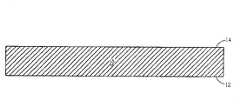
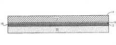
请参考图1至图16。图1至图16为本发明一优选实施例制作微型连接器的方法示意图。如图1所示,首先提供晶片10,例如硅晶片,且晶片10包括第一表面12与第二表面14。如图2所示,在晶片10的第一表面12上形成介电层16。在本实施例中,介电层16为热氧化方式形成的氧化层,其作用在提供绝缘效果,以避免漏电流问题,然介电层16的形成方式与材料并不限,例如可为沉积氧化层或由其它绝缘材料所构成。Please refer to Figure 1 to Figure 16. 1 to 16 are schematic diagrams of a method for manufacturing a micro connector according to a preferred embodiment of the present invention. As shown in FIG. 1 , firstly, a
如图3所示,对晶片10的第二表面14进行初步(preliminary)薄化工艺,例如利用粗磨(grinding)方式在不造成晶片10损坏的前提下,将晶片10的厚度迅速缩减至适当厚度。如图4所示,接着利用第一黏着层18接合介电层16与承载晶片20,使晶片10固定于承载晶片20上。在本实施例中,承载晶片20可为硅晶片、玻璃晶片、石英晶片或塑料晶片。第一黏着层18选用热释放胶带或紫外线胶带,其优点在于热释放胶带或紫外线胶带可在后续工艺中轻易利用加热或照射紫外线的方式被去除,但第一黏着层18并不限于使用上述材料,而亦可为如光致抗蚀剂、腊或聚酰亚胺(polyimide)等材料。As shown in FIG. 3 , a preliminary (preliminary) thinning process is performed on the
如图5所示,接着进行薄化工艺,由晶片10的第二表面14全面性地薄化晶片10。薄化工艺可视晶片10的最终厚度需求、表面特性需求与应力考虑等而采用不同的方法进行。举例来说,可利用等离子体蚀刻工艺全面性地薄化晶片10,由此降低先前由于粗磨工艺所产生的应力,或利用化学蚀刻工艺蚀使晶片10的第二表面14满足对于表面粗糙度的需求,亦或是利用研磨抛光(polish)工艺使晶片10的第二表面14具有所需的表面光滑度。当然,薄化工艺并不限定单独使用上述任一方式,而可视实际状况进行上述工艺的组合,或是使用其它薄化技术,例如化学机械抛光(CMP)工艺。As shown in FIG. 5 , a thinning process is performed next, and the
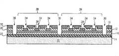
如图6所示,在薄化工艺结束后,晶片10的厚度与表面特性可符合连接器的规格要求。如图7所示,接着移除第一黏着层18,并利用第二黏着层22接合晶片10的第二表面14与承载晶片20。同样地,第二黏着层22可选用热释放胶带、紫外线胶带、光致抗蚀剂、腊或聚酰亚胺等材料。如图8所示,接着在介电层上形成导电层24,再在导电层24上形成屏蔽图案26。导电层24可为任何电性优良的材料,例如铝、金或银等,并利用电镀或沉积等方式加以形成,而屏蔽图案26则可为光致抗蚀剂图案。As shown in FIG. 6 , after the thinning process is completed, the thickness and surface characteristics of the
如图9所示,接着利用屏蔽图案26作为蚀刻掩模,蚀刻导电层24以形成导线图案28,作为连接器内部的连接线路与连接垫之用。如图10所示,去除屏蔽图案26,并接着在介电层16与导线图案28上形成绝缘层30。绝缘层30的材料可为氧化硅、氮化硅、氮氧化硅、苯环丁烯(Benzocyclobutene,BCB)或聚酰亚胺等,并依据材料不同而利用沉积或涂布等方式加以形成。As shown in FIG. 9 , using the
如图11所示,在绝缘层30上形成屏蔽图案32,例如光致抗蚀剂图案。屏蔽图案32包括对应于导线图案28的多个第一开口34,以及定义出切割道图案的多个第二开口36。如图12所示,蚀刻第一开口34暴露出的绝缘层30,以暴露出导线图案28,并一并蚀刻第二开口36暴露出的绝缘层30与介电层16。随后如图13所示,经由第二开口36利用深蚀刻技术直接蚀穿晶片10,此时晶片10已被分割为多个微型连接器38,但仍通过第二黏着层22固定于承载晶片20上。As shown in FIG. 11 , a
如图14所示,自绝缘层30的表面移除屏蔽图案32。如图15所示,自晶片10的第一表面12移除第二黏着层22。如图16所示,即制作出本发明的微型连接器38。As shown in FIG. 14 , the
综上所述,本发明制作微型连接器的方法利用热释放胶带或紫外线胶带作为黏着层的作法可有效避免制作完成的导线图案于后续工艺中受损,同时其易移除的特性亦可有效避免晶片于薄化后受损。此外,本发明先利用初步薄化工艺将晶片的厚度迅速缩减,并通过薄化工艺进一步缩减至最终厚度,同时使晶片的表面具有所欲的表面特性,再在晶片上制作出提供芯片间相互沟通的导线图案,因此可避免薄化晶片时可能产生的污染问题。再者,薄化工艺亦可消除初步薄化工艺中所产生应力,进而避免晶片产生翘曲等问题。另外,在暴露导线图案的过程中,可利用深蚀刻技术一并进行切割工艺,不仅可节省切割时间,亦可降低切割道的面积而提高装设于晶片上的芯片的密度。To sum up, the method of manufacturing the miniature connector of the present invention uses thermal release tape or ultraviolet tape as the adhesive layer, which can effectively prevent the finished wire pattern from being damaged in the subsequent process, and at the same time, its easy-to-remove feature can also effectively Avoid wafer damage after thinning. In addition, the present invention first uses the initial thinning process to rapidly reduce the thickness of the wafer, and further reduces the thickness to the final thickness through the thinning process. The communicating wire pattern thus avoids contamination problems that may arise when thinning the wafer. Furthermore, the thinning process can also eliminate the stress generated in the preliminary thinning process, thereby avoiding problems such as warping of the wafer. In addition, in the process of exposing the wire pattern, the deep etching technology can be used to perform the dicing process, which not only saves the dicing time, but also reduces the area of the dicing line and increases the density of the chips installed on the wafer.
以上所述仅为本发明的优选实施例,凡依本发明权利要求所做的等同变化与修饰,皆应属本发明的涵盖范围。The above descriptions are only preferred embodiments of the present invention, and all equivalent changes and modifications made according to the claims of the present invention shall fall within the scope of the present invention.
Claims (11)
Translated fromChinesePriority Applications (1)
| Application Number | Priority Date | Filing Date | Title |
|---|---|---|---|
| CNB2006100827310ACN100536259C (en) | 2006-05-15 | 2006-05-15 | Method for manufacturing micro connector |
Applications Claiming Priority (1)
| Application Number | Priority Date | Filing Date | Title |
|---|---|---|---|
| CNB2006100827310ACN100536259C (en) | 2006-05-15 | 2006-05-15 | Method for manufacturing micro connector |
Publications (2)
| Publication Number | Publication Date |
|---|---|
| CN101075721A CN101075721A (en) | 2007-11-21 |
| CN100536259Ctrue CN100536259C (en) | 2009-09-02 |
Family
ID=38976584
Family Applications (1)
| Application Number | Title | Priority Date | Filing Date |
|---|---|---|---|
| CNB2006100827310AExpired - Fee RelatedCN100536259C (en) | 2006-05-15 | 2006-05-15 | Method for manufacturing micro connector |
Country Status (1)
| Country | Link |
|---|---|
| CN (1) | CN100536259C (en) |
Families Citing this family (2)
| Publication number | Priority date | Publication date | Assignee | Title |
|---|---|---|---|---|
| CN101847588B (en)* | 2009-03-27 | 2012-05-09 | 台湾积体电路制造股份有限公司 | Semiconductor process |
| CN107705971A (en)* | 2017-08-30 | 2018-02-16 | 歌尔股份有限公司 | A kind of manufacture method of coil, coil, electronic equipment |
Citations (8)
| Publication number | Priority date | Publication date | Assignee | Title |
|---|---|---|---|---|
| CN1068681A (en)* | 1991-06-27 | 1993-02-03 | 三星电子株式会社 | Method for manufacturing semiconductor device |
| US5185292A (en)* | 1989-07-20 | 1993-02-09 | Harris Corporation | Process for forming extremely thin edge-connectable integrated circuit structure |
| CN1445824A (en)* | 2003-04-17 | 2003-10-01 | 威盛电子股份有限公司 | Method for preparing lugs and glue stuff layer |
| CN1510522A (en)* | 2002-12-20 | 2004-07-07 | Asml | Device manufacturing method |
| CN1534761A (en)* | 2003-03-28 | 2004-10-06 | 联华电子股份有限公司 | Method for manufacturing dual damascene structure |
| US6927471B2 (en)* | 2001-09-07 | 2005-08-09 | Peter C. Salmon | Electronic system modules and method of fabrication |
| CN1731287A (en)* | 2004-08-05 | 2006-02-08 | 探微科技股份有限公司 | Method for Etching Wafers on Both Sides |
| US20060046350A1 (en)* | 2004-08-31 | 2006-03-02 | Tongbi Jiang | Methods for fabrication of thin semiconductor assemblies including redistribution layers and packages and assemblies formed thereby |
- 2006
- 2006-05-15CNCNB2006100827310Apatent/CN100536259C/ennot_activeExpired - Fee Related
Patent Citations (8)
| Publication number | Priority date | Publication date | Assignee | Title |
|---|---|---|---|---|
| US5185292A (en)* | 1989-07-20 | 1993-02-09 | Harris Corporation | Process for forming extremely thin edge-connectable integrated circuit structure |
| CN1068681A (en)* | 1991-06-27 | 1993-02-03 | 三星电子株式会社 | Method for manufacturing semiconductor device |
| US6927471B2 (en)* | 2001-09-07 | 2005-08-09 | Peter C. Salmon | Electronic system modules and method of fabrication |
| CN1510522A (en)* | 2002-12-20 | 2004-07-07 | Asml | Device manufacturing method |
| CN1534761A (en)* | 2003-03-28 | 2004-10-06 | 联华电子股份有限公司 | Method for manufacturing dual damascene structure |
| CN1445824A (en)* | 2003-04-17 | 2003-10-01 | 威盛电子股份有限公司 | Method for preparing lugs and glue stuff layer |
| CN1731287A (en)* | 2004-08-05 | 2006-02-08 | 探微科技股份有限公司 | Method for Etching Wafers on Both Sides |
| US20060046350A1 (en)* | 2004-08-31 | 2006-03-02 | Tongbi Jiang | Methods for fabrication of thin semiconductor assemblies including redistribution layers and packages and assemblies formed thereby |
Also Published As
| Publication number | Publication date |
|---|---|
| CN101075721A (en) | 2007-11-21 |
Similar Documents
| Publication | Publication Date | Title |
|---|---|---|
| US8110900B2 (en) | Manufacturing process of semiconductor device and semiconductor device | |
| TW202021092A (en) | Post cmp processing for hybrid bonding | |
| KR20110106915A (en) | High-yield method of exposing and contacting through-silicon vias | |
| CN117878055A (en) | Stacking substrate processing | |
| TWI494979B (en) | Semiconductor process | |
| CN109166840B (en) | Multi-wafer stack structure and method of forming the same | |
| JP2004282035A (en) | Method of manufacturing semiconductor device | |
| JP2014146793A (en) | Methods of processing substrates | |
| TW201528432A (en) | Semiconductor apparatus and mothod of forming the same | |
| TWI234261B (en) | Method of forming wafer backside interconnects | |
| JP4106438B2 (en) | Multilayer fine wiring interposer and manufacturing method thereof | |
| TWI299888B (en) | Method of fabricating micro connectors | |
| CN100536259C (en) | Method for manufacturing micro connector | |
| CN105655309B (en) | Method for manufacturing interposer without chip substrate | |
| CN107424979A (en) | Method for manufacturing interposer of semiconductor device | |
| CN113937011B (en) | Chip packaging structure and manufacturing method thereof | |
| US6844626B2 (en) | Bond pad scheme for Cu process | |
| CN101847588B (en) | Semiconductor process | |
| CN100380646C (en) | Semiconductor device and manufacturing method thereof | |
| US20060162955A1 (en) | Test card assembly | |
| US8912091B2 (en) | Backside metal ground plane with improved metal adhesion and design structures | |
| CN112736060B (en) | Semiconductor structures and manufacturing methods | |
| US7833896B2 (en) | Aluminum cap for reducing scratch and wire-bond bridging of bond pads | |
| CN108122838A (en) | Semiconductor device fabrication processes | |
| CN120033148A (en) | Semiconductor wafer boundary structure and manufacturing method thereof |
Legal Events
| Date | Code | Title | Description |
|---|---|---|---|
| C06 | Publication | ||
| PB01 | Publication | ||
| C10 | Entry into substantive examination | ||
| SE01 | Entry into force of request for substantive examination | ||
| C14 | Grant of patent or utility model | ||
| GR01 | Patent grant | ||
| C17 | Cessation of patent right | ||
| CF01 | Termination of patent right due to non-payment of annual fee | Granted publication date:20090902 Termination date:20140515 |