CN100530575C - Laminating system, IC sheet, scroll of IC sheet, and method for manufacturing IC chip - Google Patents
Laminating system, IC sheet, scroll of IC sheet, and method for manufacturing IC chipDownload PDFInfo
- Publication number
- CN100530575C CN100530575CCNB2005800258794ACN200580025879ACN100530575CCN 100530575 CCN100530575 CCN 100530575CCN B2005800258794 ACNB2005800258794 ACN B2005800258794ACN 200580025879 ACN200580025879 ACN 200580025879ACN 100530575 CCN100530575 CCN 100530575C
- Authority
- CN
- China
- Prior art keywords
- thin film
- film integrated
- integrated circuit
- sheet members
- substrate
- Prior art date
- Legal status (The legal status is an assumption and is not a legal conclusion. Google has not performed a legal analysis and makes no representation as to the accuracy of the status listed.)
- Expired - Fee Related
Links
Images


Classifications
- B—PERFORMING OPERATIONS; TRANSPORTING
- B29—WORKING OF PLASTICS; WORKING OF SUBSTANCES IN A PLASTIC STATE IN GENERAL
- B29C—SHAPING OR JOINING OF PLASTICS; SHAPING OF MATERIAL IN A PLASTIC STATE, NOT OTHERWISE PROVIDED FOR; AFTER-TREATMENT OF THE SHAPED PRODUCTS, e.g. REPAIRING
- B29C65/00—Joining or sealing of preformed parts, e.g. welding of plastics materials; Apparatus therefor
- B29C65/02—Joining or sealing of preformed parts, e.g. welding of plastics materials; Apparatus therefor by heating, with or without pressure
- H—ELECTRICITY
- H10—SEMICONDUCTOR DEVICES; ELECTRIC SOLID-STATE DEVICES NOT OTHERWISE PROVIDED FOR
- H10D—INORGANIC ELECTRIC SEMICONDUCTOR DEVICES
- H10D86/00—Integrated devices formed in or on insulating or conducting substrates, e.g. formed in silicon-on-insulator [SOI] substrates or on stainless steel or glass substrates
- H10D86/01—Manufacture or treatment
- H10D86/021—Manufacture or treatment of multiple TFTs
- H10D86/0214—Manufacture or treatment of multiple TFTs using temporary substrates
- B—PERFORMING OPERATIONS; TRANSPORTING
- B32—LAYERED PRODUCTS
- B32B—LAYERED PRODUCTS, i.e. PRODUCTS BUILT-UP OF STRATA OF FLAT OR NON-FLAT, e.g. CELLULAR OR HONEYCOMB, FORM
- B32B37/00—Methods or apparatus for laminating, e.g. by curing or by ultrasonic bonding
- B32B37/0046—Methods or apparatus for laminating, e.g. by curing or by ultrasonic bonding characterised by constructional aspects of the apparatus
- B32B37/0053—Constructional details of laminating machines comprising rollers; Constructional features of the rollers
- B—PERFORMING OPERATIONS; TRANSPORTING
- B32—LAYERED PRODUCTS
- B32B—LAYERED PRODUCTS, i.e. PRODUCTS BUILT-UP OF STRATA OF FLAT OR NON-FLAT, e.g. CELLULAR OR HONEYCOMB, FORM
- B32B37/00—Methods or apparatus for laminating, e.g. by curing or by ultrasonic bonding
- B32B37/14—Methods or apparatus for laminating, e.g. by curing or by ultrasonic bonding characterised by the properties of the layers
- B32B37/16—Methods or apparatus for laminating, e.g. by curing or by ultrasonic bonding characterised by the properties of the layers with all layers existing as coherent layers before laminating
- B32B37/22—Methods or apparatus for laminating, e.g. by curing or by ultrasonic bonding characterised by the properties of the layers with all layers existing as coherent layers before laminating involving the assembly of both discrete and continuous layers
- B32B37/223—One or more of the layers being plastic
- B32B37/226—Laminating sheets, panels or inserts between two continuous plastic layers
- B—PERFORMING OPERATIONS; TRANSPORTING
- B42—BOOKBINDING; ALBUMS; FILES; SPECIAL PRINTED MATTER
- B42D—BOOKS; BOOK COVERS; LOOSE LEAVES; PRINTED MATTER CHARACTERISED BY IDENTIFICATION OR SECURITY FEATURES; PRINTED MATTER OF SPECIAL FORMAT OR STYLE NOT OTHERWISE PROVIDED FOR; DEVICES FOR USE THEREWITH AND NOT OTHERWISE PROVIDED FOR; MOVABLE-STRIP WRITING OR READING APPARATUS
- B42D25/00—Information-bearing cards or sheet-like structures characterised by identification or security features; Manufacture thereof
- B42D25/40—Manufacture
- B42D25/45—Associating two or more layers
- G—PHYSICS
- G06—COMPUTING OR CALCULATING; COUNTING
- G06K—GRAPHICAL DATA READING; PRESENTATION OF DATA; RECORD CARRIERS; HANDLING RECORD CARRIERS
- G06K19/00—Record carriers for use with machines and with at least a part designed to carry digital markings
- G06K19/06—Record carriers for use with machines and with at least a part designed to carry digital markings characterised by the kind of the digital marking, e.g. shape, nature, code
- G06K19/067—Record carriers with conductive marks, printed circuits or semiconductor circuit elements, e.g. credit or identity cards also with resonating or responding marks without active components
- G06K19/07—Record carriers with conductive marks, printed circuits or semiconductor circuit elements, e.g. credit or identity cards also with resonating or responding marks without active components with integrated circuit chips
- G06K19/077—Constructional details, e.g. mounting of circuits in the carrier
- G06K19/07718—Constructional details, e.g. mounting of circuits in the carrier the record carrier being manufactured in a continuous process, e.g. using endless rolls
- H—ELECTRICITY
- H01—ELECTRIC ELEMENTS
- H01L—SEMICONDUCTOR DEVICES NOT COVERED BY CLASS H10
- H01L24/00—Arrangements for connecting or disconnecting semiconductor or solid-state bodies; Methods or apparatus related thereto
- H01L24/80—Methods for connecting semiconductor or other solid state bodies using means for bonding being attached to, or being formed on, the surface to be connected
- H01L24/86—Methods for connecting semiconductor or other solid state bodies using means for bonding being attached to, or being formed on, the surface to be connected using tape automated bonding [TAB]
- H—ELECTRICITY
- H10—SEMICONDUCTOR DEVICES; ELECTRIC SOLID-STATE DEVICES NOT OTHERWISE PROVIDED FOR
- H10D—INORGANIC ELECTRIC SEMICONDUCTOR DEVICES
- H10D86/00—Integrated devices formed in or on insulating or conducting substrates, e.g. formed in silicon-on-insulator [SOI] substrates or on stainless steel or glass substrates
- H10D86/40—Integrated devices formed in or on insulating or conducting substrates, e.g. formed in silicon-on-insulator [SOI] substrates or on stainless steel or glass substrates characterised by multiple TFTs
- H10D86/60—Integrated devices formed in or on insulating or conducting substrates, e.g. formed in silicon-on-insulator [SOI] substrates or on stainless steel or glass substrates characterised by multiple TFTs wherein the TFTs are in active matrices
- B—PERFORMING OPERATIONS; TRANSPORTING
- B32—LAYERED PRODUCTS
- B32B—LAYERED PRODUCTS, i.e. PRODUCTS BUILT-UP OF STRATA OF FLAT OR NON-FLAT, e.g. CELLULAR OR HONEYCOMB, FORM
- B32B2425/00—Cards, e.g. identity cards, credit cards
- H—ELECTRICITY
- H01—ELECTRIC ELEMENTS
- H01L—SEMICONDUCTOR DEVICES NOT COVERED BY CLASS H10
- H01L2224/00—Indexing scheme for arrangements for connecting or disconnecting semiconductor or solid-state bodies and methods related thereto as covered by H01L24/00
- H01L2224/74—Apparatus for manufacturing arrangements for connecting or disconnecting semiconductor or solid-state bodies and for methods related thereto
- H01L2224/79—Apparatus for Tape Automated Bonding [TAB]
- H01L2224/7965—Means for transporting the components to be connected
- H—ELECTRICITY
- H01—ELECTRIC ELEMENTS
- H01L—SEMICONDUCTOR DEVICES NOT COVERED BY CLASS H10
- H01L2924/00—Indexing scheme for arrangements or methods for connecting or disconnecting semiconductor or solid-state bodies as covered by H01L24/00
- H01L2924/01—Chemical elements
- H01L2924/01002—Helium [He]
- H—ELECTRICITY
- H01—ELECTRIC ELEMENTS
- H01L—SEMICONDUCTOR DEVICES NOT COVERED BY CLASS H10
- H01L2924/00—Indexing scheme for arrangements or methods for connecting or disconnecting semiconductor or solid-state bodies as covered by H01L24/00
- H01L2924/01—Chemical elements
- H01L2924/01004—Beryllium [Be]
- H—ELECTRICITY
- H01—ELECTRIC ELEMENTS
- H01L—SEMICONDUCTOR DEVICES NOT COVERED BY CLASS H10
- H01L2924/00—Indexing scheme for arrangements or methods for connecting or disconnecting semiconductor or solid-state bodies as covered by H01L24/00
- H01L2924/01—Chemical elements
- H01L2924/01005—Boron [B]
- H—ELECTRICITY
- H01—ELECTRIC ELEMENTS
- H01L—SEMICONDUCTOR DEVICES NOT COVERED BY CLASS H10
- H01L2924/00—Indexing scheme for arrangements or methods for connecting or disconnecting semiconductor or solid-state bodies as covered by H01L24/00
- H01L2924/01—Chemical elements
- H01L2924/01006—Carbon [C]
- H—ELECTRICITY
- H01—ELECTRIC ELEMENTS
- H01L—SEMICONDUCTOR DEVICES NOT COVERED BY CLASS H10
- H01L2924/00—Indexing scheme for arrangements or methods for connecting or disconnecting semiconductor or solid-state bodies as covered by H01L24/00
- H01L2924/01—Chemical elements
- H01L2924/01013—Aluminum [Al]
- H—ELECTRICITY
- H01—ELECTRIC ELEMENTS
- H01L—SEMICONDUCTOR DEVICES NOT COVERED BY CLASS H10
- H01L2924/00—Indexing scheme for arrangements or methods for connecting or disconnecting semiconductor or solid-state bodies as covered by H01L24/00
- H01L2924/01—Chemical elements
- H01L2924/01015—Phosphorus [P]
- H—ELECTRICITY
- H01—ELECTRIC ELEMENTS
- H01L—SEMICONDUCTOR DEVICES NOT COVERED BY CLASS H10
- H01L2924/00—Indexing scheme for arrangements or methods for connecting or disconnecting semiconductor or solid-state bodies as covered by H01L24/00
- H01L2924/01—Chemical elements
- H01L2924/01024—Chromium [Cr]
- H—ELECTRICITY
- H01—ELECTRIC ELEMENTS
- H01L—SEMICONDUCTOR DEVICES NOT COVERED BY CLASS H10
- H01L2924/00—Indexing scheme for arrangements or methods for connecting or disconnecting semiconductor or solid-state bodies as covered by H01L24/00
- H01L2924/01—Chemical elements
- H01L2924/01027—Cobalt [Co]
- H—ELECTRICITY
- H01—ELECTRIC ELEMENTS
- H01L—SEMICONDUCTOR DEVICES NOT COVERED BY CLASS H10
- H01L2924/00—Indexing scheme for arrangements or methods for connecting or disconnecting semiconductor or solid-state bodies as covered by H01L24/00
- H01L2924/01—Chemical elements
- H01L2924/01029—Copper [Cu]
- H—ELECTRICITY
- H01—ELECTRIC ELEMENTS
- H01L—SEMICONDUCTOR DEVICES NOT COVERED BY CLASS H10
- H01L2924/00—Indexing scheme for arrangements or methods for connecting or disconnecting semiconductor or solid-state bodies as covered by H01L24/00
- H01L2924/01—Chemical elements
- H01L2924/01033—Arsenic [As]
- H—ELECTRICITY
- H01—ELECTRIC ELEMENTS
- H01L—SEMICONDUCTOR DEVICES NOT COVERED BY CLASS H10
- H01L2924/00—Indexing scheme for arrangements or methods for connecting or disconnecting semiconductor or solid-state bodies as covered by H01L24/00
- H01L2924/01—Chemical elements
- H01L2924/01041—Niobium [Nb]
- H—ELECTRICITY
- H01—ELECTRIC ELEMENTS
- H01L—SEMICONDUCTOR DEVICES NOT COVERED BY CLASS H10
- H01L2924/00—Indexing scheme for arrangements or methods for connecting or disconnecting semiconductor or solid-state bodies as covered by H01L24/00
- H01L2924/01—Chemical elements
- H01L2924/01042—Molybdenum [Mo]
- H—ELECTRICITY
- H01—ELECTRIC ELEMENTS
- H01L—SEMICONDUCTOR DEVICES NOT COVERED BY CLASS H10
- H01L2924/00—Indexing scheme for arrangements or methods for connecting or disconnecting semiconductor or solid-state bodies as covered by H01L24/00
- H01L2924/01—Chemical elements
- H01L2924/01049—Indium [In]
- H—ELECTRICITY
- H01—ELECTRIC ELEMENTS
- H01L—SEMICONDUCTOR DEVICES NOT COVERED BY CLASS H10
- H01L2924/00—Indexing scheme for arrangements or methods for connecting or disconnecting semiconductor or solid-state bodies as covered by H01L24/00
- H01L2924/01—Chemical elements
- H01L2924/01056—Barium [Ba]
- H—ELECTRICITY
- H01—ELECTRIC ELEMENTS
- H01L—SEMICONDUCTOR DEVICES NOT COVERED BY CLASS H10
- H01L2924/00—Indexing scheme for arrangements or methods for connecting or disconnecting semiconductor or solid-state bodies as covered by H01L24/00
- H01L2924/01—Chemical elements
- H01L2924/0106—Neodymium [Nd]
- H—ELECTRICITY
- H01—ELECTRIC ELEMENTS
- H01L—SEMICONDUCTOR DEVICES NOT COVERED BY CLASS H10
- H01L2924/00—Indexing scheme for arrangements or methods for connecting or disconnecting semiconductor or solid-state bodies as covered by H01L24/00
- H01L2924/01—Chemical elements
- H01L2924/01073—Tantalum [Ta]
- H—ELECTRICITY
- H01—ELECTRIC ELEMENTS
- H01L—SEMICONDUCTOR DEVICES NOT COVERED BY CLASS H10
- H01L2924/00—Indexing scheme for arrangements or methods for connecting or disconnecting semiconductor or solid-state bodies as covered by H01L24/00
- H01L2924/01—Chemical elements
- H01L2924/01074—Tungsten [W]
- H—ELECTRICITY
- H01—ELECTRIC ELEMENTS
- H01L—SEMICONDUCTOR DEVICES NOT COVERED BY CLASS H10
- H01L2924/00—Indexing scheme for arrangements or methods for connecting or disconnecting semiconductor or solid-state bodies as covered by H01L24/00
- H01L2924/01—Chemical elements
- H01L2924/01079—Gold [Au]
- H—ELECTRICITY
- H01—ELECTRIC ELEMENTS
- H01L—SEMICONDUCTOR DEVICES NOT COVERED BY CLASS H10
- H01L2924/00—Indexing scheme for arrangements or methods for connecting or disconnecting semiconductor or solid-state bodies as covered by H01L24/00
- H01L2924/01—Chemical elements
- H01L2924/01082—Lead [Pb]
- H—ELECTRICITY
- H01—ELECTRIC ELEMENTS
- H01L—SEMICONDUCTOR DEVICES NOT COVERED BY CLASS H10
- H01L2924/00—Indexing scheme for arrangements or methods for connecting or disconnecting semiconductor or solid-state bodies as covered by H01L24/00
- H01L2924/049—Nitrides composed of metals from groups of the periodic table
- H01L2924/0495—5th Group
- H01L2924/04953—TaN
- H—ELECTRICITY
- H01—ELECTRIC ELEMENTS
- H01L—SEMICONDUCTOR DEVICES NOT COVERED BY CLASS H10
- H01L2924/00—Indexing scheme for arrangements or methods for connecting or disconnecting semiconductor or solid-state bodies as covered by H01L24/00
- H01L2924/095—Indexing scheme for arrangements or methods for connecting or disconnecting semiconductor or solid-state bodies as covered by H01L24/00 with a principal constituent of the material being a combination of two or more materials provided in the groups H01L2924/013 - H01L2924/0715
- H01L2924/097—Glass-ceramics, e.g. devitrified glass
- H01L2924/09701—Low temperature co-fired ceramic [LTCC]
- H—ELECTRICITY
- H01—ELECTRIC ELEMENTS
- H01L—SEMICONDUCTOR DEVICES NOT COVERED BY CLASS H10
- H01L2924/00—Indexing scheme for arrangements or methods for connecting or disconnecting semiconductor or solid-state bodies as covered by H01L24/00
- H01L2924/10—Details of semiconductor or other solid state devices to be connected
- H01L2924/11—Device type
- H01L2924/14—Integrated circuits
- H—ELECTRICITY
- H01—ELECTRIC ELEMENTS
- H01L—SEMICONDUCTOR DEVICES NOT COVERED BY CLASS H10
- H01L2924/00—Indexing scheme for arrangements or methods for connecting or disconnecting semiconductor or solid-state bodies as covered by H01L24/00
- H01L2924/15—Details of package parts other than the semiconductor or other solid state devices to be connected
- H01L2924/151—Die mounting substrate
- H01L2924/156—Material
- H01L2924/15786—Material with a principal constituent of the material being a non metallic, non metalloid inorganic material
- H01L2924/15787—Ceramics, e.g. crystalline carbides, nitrides or oxides
- H—ELECTRICITY
- H01—ELECTRIC ELEMENTS
- H01L—SEMICONDUCTOR DEVICES NOT COVERED BY CLASS H10
- H01L2924/00—Indexing scheme for arrangements or methods for connecting or disconnecting semiconductor or solid-state bodies as covered by H01L24/00
- H01L2924/19—Details of hybrid assemblies other than the semiconductor or other solid state devices to be connected
- H01L2924/1901—Structure
- H01L2924/1904—Component type
- H01L2924/19041—Component type being a capacitor
Landscapes
- Engineering & Computer Science (AREA)
- Computer Hardware Design (AREA)
- Microelectronics & Electronic Packaging (AREA)
- Physics & Mathematics (AREA)
- General Physics & Mathematics (AREA)
- Theoretical Computer Science (AREA)
- Power Engineering (AREA)
- Mechanical Engineering (AREA)
- Manufacturing & Machinery (AREA)
- Encapsulation Of And Coatings For Semiconductor Or Solid State Devices (AREA)
Abstract
Translated fromChinese
Description
Translated fromChinese技术领域technical field
本发明涉及一种用于剥离和密封提供在衬底上方的薄膜集成电路的层压系统、包括多个密封的薄膜集成电路的IC薄片、包括多个密封的薄膜集成电路的IC薄片卷、以及用于制造密封薄膜集成电路的IC芯片的方法。The present invention relates to a lamination system for peeling and sealing a thin film integrated circuit provided over a substrate, an IC wafer including a plurality of sealed thin film integrated circuits, an IC wafer roll including a plurality of sealed thin film integrated circuits, and A method for manufacturing IC chips that encapsulate thin film integrated circuits.
背景技术Background technique
近年来,在需要自动识别的领域中,例如在有价证券和商品管理中,对安装有IC芯片的卡片或能够非接触传输数据的安装了的IC芯片的标签的需求一直在增长。该安装了IC芯片的卡片经由卡片内的环形天线从外部器件读取数据/将数据写到外部器件。该安装了IC芯片的卡片具有比通过磁性编码方法记录数据的磁卡更大的存储容量且更安全。因此,已经提议,安装了IC的卡片的形式能够被应用到不同的领域。 (例如,参考专利文献1。)In recent years, demands for IC chip-mounted cards or IC chip-mounted tags capable of non-contact transmission of data have been increasing in fields requiring automatic identification, such as securities and commodity management. This IC chip-mounted card reads/writes data from/to an external device via a loop antenna inside the card. The IC chip-mounted card has a larger storage capacity and is more secure than a magnetic card in which data is recorded by a magnetic encoding method. Therefore, it has been proposed that the form of the IC-mounted card can be applied to various fields. (For example, refer to
通常,IC芯片由硅晶片形成。近年来,利用提供在玻璃衬底上方的薄膜集成电路的IC芯片(IC标签、ID标签、RF标签(射频)、无线标签(也称为电子标签))的技术发展已促进了成本降低。根据这种技术,在完全地制造完之后,提供在玻璃衬底上方的该薄膜集成电路需要与作为支撑衬底的玻璃衬底分离。因此,已经发明了各种不同的技术作为分离提供在支撑衬底上的薄膜集成电路的方法。Typically, IC chips are formed from silicon wafers. In recent years, technological development of IC chips (IC tags, ID tags, RF tags (radio frequency), wireless tags (also called electronic tags)) using thin film integrated circuits provided over glass substrates has contributed to cost reduction. According to this technique, the thin film integrated circuit provided over the glass substrate needs to be separated from the glass substrate as a supporting substrate after it is completely manufactured. Therefore, various techniques have been invented as a method of separating thin film integrated circuits provided on a support substrate.
例如,作为剥离提供在支撑衬底上方的薄膜集成电路的方法,有这样的技术:形成由非晶硅(或多晶硅)制成的剥离层,并通过激光照射释放包含于非晶硅内的氢,以产生真空区,将支撑衬底从剥离层分离(专利文献2)。可选地,还有这样一种技术:在薄膜集成电路和支撑衬底之间形成含硅的剥离层,并用含卤素氟化物的气体移除该剥离层,以将薄膜集成电路从支撑衬底分离(专利文献3)。For example, as a method of peeling off a thin film integrated circuit provided over a supporting substrate, there is a technique of forming a peeling layer made of amorphous silicon (or polysilicon) and releasing hydrogen contained in the amorphous silicon by laser irradiation , to generate a vacuum zone to separate the supporting substrate from the peeling layer (Patent Document 2). Alternatively, there is also a technique of forming a release layer containing silicon between the thin film integrated circuit and the support substrate, and removing the release layer with a gas containing halogen fluoride to release the thin film integrated circuit from the support substrate. Separation (Patent Document 3).
专利文献1:未审专利公开No.2001-260580Patent Document 1: Unexamined Patent Publication No. 2001-260580
专利文献2:未审专利公开No.10-125929Patent Document 2: Unexamined Patent Publication No. 10-125929
专利文献3:未审专利公开No.8-254686Patent Document 3: Unexamined Patent Publication No. 8-254686
然而,在衬底上方形成多个薄膜集成电路的情况下,通过移除该剥离层将该多个薄膜集成电路单独地从衬底分离。当通过层压处理等分别密封分离的薄膜集成电路时,制造效率就退化了。由于分离的薄膜集成电路薄并且重量轻,所以在没有损害或破裂的情况下密封它们非常困难。However, in the case of forming a plurality of thin film integrated circuits over a substrate, the plurality of thin film integrated circuits are individually separated from the substrate by removing the peeling layer. When separate thin film integrated circuits are individually sealed by a lamination process or the like, manufacturing efficiency is degraded. Since the separated thin film integrated circuits are thin and lightweight, it is very difficult to seal them without damage or cracking.
从生产效率的观点来看,通过利用一系列设备,对提供在衬底上方的薄膜集成电路接连地进行剥离和密封工艺。通常,考虑到密封之后的强度和可靠性,用具有强粘附力的膜例如热熔性膜进行通过层压处理的密封工艺。因此,当也用具有强粘附力的膜进行对薄膜集成电路的剥离工艺时,因为该膜会粘附在衬底上,所以薄膜集成电路的剥离可能失败。结果,出现制造产量退化的问题。在用具有弱粘附的膜进行对薄膜集成电路的剥离和密封工艺的情况下,薄膜集成电路可以有效地从衬底上剥离;然而,出现密封的薄膜集成电路的可靠性问题。From the viewpoint of production efficiency, the peeling and sealing processes are successively performed on the thin film integrated circuits provided over the substrate by using a series of equipment. Generally, the sealing process by lamination is performed with a film having strong adhesive force such as a hot-melt film in consideration of strength and reliability after sealing. Therefore, when the lift-off process of the thin film integrated circuit is also performed with a film having a strong adhesive force, the lift-off of the thin film integrated circuit may fail because the film may adhere to the substrate. As a result, there arises a problem of degradation in manufacturing yield. In the case where the peeling and sealing process of the thin film integrated circuit is performed with a film having weak adhesion, the thin film integrated circuit can be effectively peeled from the substrate; however, a reliability problem of the sealed thin film integrated circuit arises.
发明内容Contents of the invention
考虑到前述的问题,本发明的一个目的是:在密封薄膜集成电路时防止制造效率退化,并防止薄膜集成电路的损害和破坏。此外,本发明的另一个目的是:从衬底剥离薄膜集成电路并密封剥离的薄膜集成电路,以及提高制造产量。In view of the aforementioned problems, an object of the present invention is to prevent degradation of manufacturing efficiency and to prevent damage and destruction of thin film integrated circuits when sealing thin film integrated circuits. Furthermore, another object of the present invention is to peel a thin film integrated circuit from a substrate and seal the peeled thin film integrated circuit, and to improve manufacturing yield.
本发明的一个实施例提供一种层压系统,包括:传送装置,用于传送提供有多个薄膜集成电路的衬底;第一剥离装置,用于将薄膜集成电路的第一表面结合到第一薄片构件,以从该衬底剥离该薄膜集成电路;第二剥离装置,用于将与薄膜集成电路的第一表面相对的第二表面结合到第二薄片构件,以从第一薄片构件剥离薄膜集成电路;和密封装置,用于在第二薄片构件和第三薄片构件之间插入该薄膜集成电路,以用第二薄片构件和第三薄片构件密封该薄膜集成电路。One embodiment of the present invention provides a lamination system, including: a transfer device for transferring a substrate provided with a plurality of thin film integrated circuits; a first peeling device for bonding the first surface of the thin film integrated circuits to the first surface of the thin film integrated circuits. a sheet member to peel off the thin film integrated circuit from the substrate; a second peeling device for bonding a second surface opposite to the first surface of the thin film integrated circuit to the second sheet member to peel off from the first sheet member a thin film integrated circuit; and sealing means for interposing the thin film integrated circuit between the second sheet member and the third sheet member to seal the thin film integrated circuit with the second sheet member and the third sheet member.
本发明的另一个实施例提供一种层压系统,包括:传送装置,用于传送提供有多个薄膜集成电路的衬底;缠绕有第一薄片构件的第一供应辊;第一剥离装置,用于将薄膜集成电路的第一表面结合到第一薄片构件,以从该衬底上剥离该薄膜集成电路;缠绕有第二薄片构件的第二供应辊;第二剥离装置,用于将薄膜集成电路的相对第一表面的第二表面结合到第二薄片构件,以从第一薄片构件剥离薄膜集成电路;缠绕有第三薄片构件的第三供应辊;密封装置,用于在第二薄片构件和第三薄片构件之间插入该薄膜集成电路,以用第二薄片构件和第三薄片构件密封该薄膜集成电路;和接收辊;用于缠绕用第二薄片构件和第三薄片构件密封的薄膜集成电路。Another embodiment of the present invention provides a lamination system including: a transfer device for transferring a substrate provided with a plurality of thin film integrated circuits; a first supply roll wound with a first sheet member; a first peeling device, for bonding the first surface of the thin film integrated circuit to the first sheet member to peel the thin film integrated circuit from the substrate; a second supply roll wound with the second sheet member; a second peeling device for attaching the thin film The second surface of the integrated circuit opposite to the first surface is bonded to the second sheet member to peel the thin film integrated circuit from the first sheet member; a third supply roll is wound with the third sheet member; The thin film integrated circuit is inserted between the member and the third sheet member to seal the thin film integrated circuit with the second sheet member and the third sheet member; and a receiving roller; for winding the sealed film with the second sheet member and the third sheet member thin film integrated circuits.
本发明的另一个实施例提供一种层压系统,包括:提供有多个薄膜集成电路的衬底;缠绕第一薄片构件的第一供应辊;固定和移动装置,用于固定衬底以便衬底的一个表面与第一薄片构件相对,以及用于移动衬底以便多个薄膜集成电路和第一薄片构件粘合在一起;第一剥离装置,用于将薄膜集成电路的第一表面结合到第一薄片构件,以从衬底剥离薄膜集成电路;缠绕第二薄片的第二供应辊;第二剥离装置,用于将薄膜集成电路的相对第一表面的第二表面结合到第二薄片构件,以从第一薄片构件剥离该薄膜集成电路;缠绕第三薄片构件的第三供应辊,该第三薄片构件结合到薄膜集成电路的第一表面;密封装置,用于用第二薄片构件和第三薄片构件密封薄膜集成电路;和接收辊,用于缠绕用第二薄片构件和第三薄片构件密封的薄膜集成电路。Another embodiment of the present invention provides a lamination system including: a substrate provided with a plurality of thin film integrated circuits; a first supply roll wound around a first sheet member; a fixing and moving device for fixing the substrate so that the substrate One surface of the bottom is opposite to the first sheet member, and is used to move the substrate so that a plurality of thin film integrated circuits and the first sheet member are bonded together; a first peeling device is used to bond the first surface of the thin film integrated circuit to the a first sheet member to peel the thin film integrated circuit from the substrate; a second supply roll winding the second sheet; a second peeling device for bonding a second surface of the thin film integrated circuit opposite to the first surface to the second sheet member , to peel the thin film integrated circuit from the first sheet member; a third supply roll winding a third sheet member bonded to the first surface of the thin film integrated circuit; sealing means for using the second sheet member and The third sheet member seals the thin film integrated circuit; and a take-up roller for winding the thin film integrated circuit sealed with the second sheet member and the third sheet member.
在具有前述实施例的层压系统中,密封装置具有使得彼此相对提供的至少两个辊。两个辊的任一个或两个具有加热装置。该密封装置使薄膜集成电路穿过这两个辊,并通过进行加压处理和加热处理的任一种或两种来密封薄膜集成电路。In the lamination system with the foregoing embodiments, the sealing device has at least two rollers provided so as to face each other. Either one or both of the two rollers have heating means. The sealing device passes the thin film integrated circuits through the two rollers, and seals the thin film integrated circuits by performing either one or both of pressure treatment and heat treatment.
本发明的再一个实施例提供一种层压系统,包括:传送装置,用于传送提供有多个薄膜集成电路的衬底;缠绕第一薄片构件的第一供应辊;第一剥离装置,用于将薄膜集成电路的第一表面结合到第一薄片构件,以从衬底剥离薄膜集成电路;缠绕第二薄片构件的第二供应辊;第二剥离装置,用于将薄膜集成电路的相对第一表面的第二表面结合到第二薄片构件,以从第一薄片构件剥离该薄膜集成电路;用于通过挤压到薄膜集成电路的第一表面上,供应加热和熔融态树脂的装置;密封装置,用于用第二薄片构件和树脂密封薄膜集成电路;和接收辊,用于缠绕用第二薄片构件和树脂密封的薄膜集成电路。在该种情况下,该密封装置至少具有两个彼此相对提供的辊,两个辊的任一个或两个都具有冷却装置。密封装置将薄膜集成电路传过这两个辊,并通过进行加压处理和加热处理的任一种或两种来密封薄膜集成电路。Still another embodiment of the present invention provides a lamination system including: a transfer device for transferring a substrate provided with a plurality of thin film integrated circuits; a first supply roll winding a first sheet member; a first peeling device for for bonding the first surface of the thin film integrated circuit to the first sheet member to peel the thin film integrated circuit from the substrate; a second supply roll winding the second sheet member; A second surface of one surface is bonded to a second sheet member to peel the thin film integrated circuit from the first sheet member; means for supplying heat and molten resin by extrusion onto the first surface of the thin film integrated circuit; sealing a device for sealing the thin film integrated circuit with the second sheet member and the resin; and a take-up roll for winding the thin film integrated circuit sealed with the second sheet member and the resin. In this case, the sealing device has at least two rollers provided opposite each other, either or both of which are provided with cooling means. The sealing device passes the thin film integrated circuits through the two rollers, and seals the thin film integrated circuits by performing either one or both of pressure treatment and heat treatment.
在根据本发明的层压系统中,第一剥离装置和第二剥离装置具有辊。此外,第二剥离装置具有至少两个彼此相对的辊,将薄膜集成电路穿过这两个辊,并通过进行加压处理和加热处理的任一种或两种来密封薄膜集成电路。In the lamination system according to the invention, the first peeling device and the second peeling device have rollers. In addition, the second peeling device has at least two rollers facing each other, passes the thin film integrated circuit through the two rollers, and seals the thin film integrated circuit by performing either one or both of pressure treatment and heat treatment.
第一薄片构件有至少一个具有粘附性质的侧面。第二薄片构件和第三薄片构件是层压膜。The first sheet member has at least one side having adhesive properties. The second sheet member and the third sheet member are laminated films.
本发明提供一种IC薄片,通过将多个密封的薄膜集成电路形成为薄片形成该IC薄片使得该IC薄片更容易被使用。根据本发明的IC薄片包括第二薄片构件和第三薄片构件两个薄片构件,在第二薄片构件和第三薄片构件之间密封多个薄膜集成电路。The present invention provides an IC chip which is formed by forming a plurality of sealed thin film integrated circuits into a chip so that the IC chip can be more easily used. An IC chip according to the present invention includes two sheet members, a second sheet member and a third sheet member, between which a plurality of thin film integrated circuits are sealed.
本发明提供一种IC薄片卷,通过缠绕包括用两个薄片构件密封多个的薄膜集成电路的IC薄片形成该IC薄片卷,使得IC薄片卷更容易被使用。通过缠绕由在第二薄片构件和第三薄片构件两个薄片构件之间密封多个薄膜集成电路获得的IC薄片来形成根据本发明的IC薄片卷。The present invention provides an IC sheet roll formed by winding an IC sheet including a plurality of thin film integrated circuits sealed with two sheet members so that the IC sheet roll can be used more easily. The IC sheet roll according to the present invention is formed by winding an IC sheet obtained by sealing a plurality of thin film integrated circuits between two sheet members of a second sheet member and a third sheet member.
在具有前述实施例的IC薄片或IC薄片卷中,多个薄膜集成电路的每一个都具有多个薄膜晶体管和用作天线的导电层,且多个薄膜集成电路的每一个有规则地布置。In the IC chip or IC chip roll with the foregoing embodiments, each of the plurality of thin film integrated circuits has a plurality of thin film transistors and a conductive layer serving as an antenna, and each of the plurality of thin film integrated circuits is regularly arranged.
一种用于制造IC芯片的方法,包括步骤:在具有绝缘表面的衬底上方形成剥离层;在衬底上方形成多个薄膜集成电路;在薄膜集成电路之间的边界处形成开口部分,以暴露出剥离层;将包含卤素氟化物的气体或液体引入到开口部分中以移除剥离层;将薄膜集成电路的第一表面结合到第一薄片构件,以从衬底剥离多个薄膜集成电路;将薄膜集成电路的相对第一表面的第二表面结合到第二薄片构件,以从第一薄片构件剥离薄膜集成电路;将薄膜集成电路的第一表面结合到第三薄片构件,以用第二薄片构件和第三薄片构件密封薄膜集成电路。此外,在衬底上方形成多个薄膜晶体管和用作天线的导电层作为薄膜集成电路。A method for manufacturing an IC chip, comprising the steps of: forming a peeling layer over a substrate having an insulating surface; forming a plurality of thin film integrated circuits over the substrate; forming an opening portion at a boundary between the thin film integrated circuits, to exposing the peeling layer; introducing a gas or liquid containing halogen fluoride into the opening portion to remove the peeling layer; bonding the first surface of the thin film integrated circuit to the first sheet member to peel the plurality of thin film integrated circuits from the substrate ; bonding the second surface of the thin film integrated circuit opposite to the first surface to the second sheet member to peel the thin film integrated circuit from the first sheet member; bonding the first surface of the thin film integrated circuit to the third sheet member to use the second sheet member The second sheet member and the third sheet member seal the thin film integrated circuit. In addition, a plurality of thin film transistors and a conductive layer serving as an antenna are formed as a thin film integrated circuit over the substrate.
附图说明Description of drawings
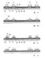
图1是用于示出根据本发明的层压系统的图;FIG. 1 is a diagram for illustrating a lamination system according to the present invention;
图2是用于示出根据本发明的层压系统的图;Figure 2 is a diagram for illustrating a lamination system according to the present invention;
图3是用于示出根据本发明的层压系统的图;Figure 3 is a diagram for illustrating a lamination system according to the present invention;
图4是用于示出根据本发明的层压系统的图;Figure 4 is a diagram for illustrating a lamination system according to the present invention;
图5A和5B是用于示出根据本发明的IC薄片的图;5A and 5B are diagrams for illustrating an IC chip according to the present invention;
图6A和6B是用于示出根据本发明的IC薄片的辊的图;6A and 6B are diagrams for illustrating a roll of an IC wafer according to the present invention;
图7A至7C是用于示出根据本发明制造IC芯片的方法的图;7A to 7C are diagrams for illustrating a method of manufacturing an IC chip according to the present invention;
图8A至8C是用于示出根据本发明制造IC芯片的方法的图;8A to 8C are diagrams for illustrating a method of manufacturing an IC chip according to the present invention;
图9A和9B是用于示出根据本发明制造IC芯片的方法的图;9A and 9B are diagrams for illustrating a method of manufacturing an IC chip according to the present invention;
图10A和10B是用于示出根据本发明的剥离方法的图;10A and 10B are diagrams for illustrating a peeling method according to the present invention;
图11A和11B是用于示出根据本发明的IC芯片的顶视图的图;11A and 11B are diagrams for showing a top view of an IC chip according to the present invention;
图12A至12E是用于示出根据本发明安装有薄膜集成电路的物品的图;12A to 12E are diagrams for illustrating an article mounted with a thin film integrated circuit according to the present invention;
图13A和13B是用于示出根据本发明安装有薄膜集成电路的物品的图;13A and 13B are diagrams for illustrating an article mounted with a thin film integrated circuit according to the present invention;
图14是用于示出根据本发明的IC芯片的截面结构的图;14 is a diagram for illustrating a cross-sectional structure of an IC chip according to the present invention;
图15A和15B是用于示出根据本发明的IC芯片的截面结构的图;和15A and 15B are diagrams for illustrating a cross-sectional structure of an IC chip according to the present invention; and
图16A和16B是用于示出根据本发明的IC芯片的截面结构的图。16A and 16B are diagrams for illustrating a cross-sectional structure of an IC chip according to the present invention.
具体实施方式Detailed ways
当连同附图阅读本发明时,由下面的详细描述,将更充分地展现本发明的上述的和其它目的以及新颖的特征。由于本发明可以以几种方式具体化,所以要明白,各种变化和修改对于本领域的技术人员来说是显而易见的,而不偏离本发明的基本特征的范围。因此,除非其它方面的这种变化和修改偏离了在下文中描述的本发明的范围,否则它们解释为包含在其中。在实施例的图中,相似的部分用与第一实施例相似的参考数字表示,并且将不再说明。The above and other objects and novel features of the invention will appear more fully from the following detailed description when the invention is read in conjunction with the accompanying drawings. Since the present invention can be embodied in several ways, it is to be understood that various changes and modifications will be apparent to those skilled in the art without departing from the scope of the essential characteristics of the invention. Therefore, unless otherwise such changes and modifications depart from the scope of the present invention described hereinafter, they are to be construed as being included therein. In the drawings of the embodiment, like parts are denoted by like reference numerals as those of the first embodiment, and will not be described again.
本发明提供一种层压系统,其连续地剥离提供在衬底上方的薄膜集成电路和密封该剥离的薄膜集成电路。根据本发明,提供在衬底上方的多个薄膜集成电路结合到第一薄片构件,以从衬底上剥离该薄膜集成电路;结合到第一薄片构件的薄膜集成电路结合到第二薄片构件,以再一次从第一薄片构件上剥离该薄膜集成电路;然后,将第三薄片构件结合到与第二薄片构件粘合的表面相对的表面;然后,通过密封装置用第二薄片构件和第三薄片构件密封薄膜集成电路。也就是,在一系列剥离和密封的工艺中,薄膜集成电路的剥离进行两次。The present invention provides a lamination system that continuously peels off a thin film integrated circuit provided over a substrate and seals the peeled thin film integrated circuit. According to the present invention, it is provided that a plurality of thin film integrated circuits bonded to the first sheet member over the substrate to peel the thin film integrated circuits from the substrate; the thin film integrated circuits bonded to the first sheet member are bonded to the second sheet member, To peel off the thin film integrated circuit from the first sheet member again; then, the third sheet member is bonded to the surface opposite to the surface where the second sheet member is bonded; then, the second sheet member and the third sheet member are sealed by the sealing device. The sheet member seals the thin film integrated circuit. That is, in a series of processes of peeling and sealing, the peeling of the thin film integrated circuit is performed twice.
第一薄片构件用于剥离提供在衬底上方的薄膜集成电路。第二薄片构件用于从第一薄片构件剥离该薄膜集成电路,并用作层压膜以和第三薄片构件密封薄膜集成电路。进行两次剥离的原因是:因为层压膜不仅粘附到薄膜集成电路还粘附在衬底上,用于密封的层压膜具有很强的粘附力,以致于提供在衬底上的薄膜集成电路不能从该衬底上有效地剥离。因此,具有弱粘附表面的第一薄片构件用于剥离衬底上的薄膜集成电路,并且由层压膜等形成的第二薄片构件用于从第一薄片构件上再次剥离薄膜集成电路。The first sheet member is used for peeling off the thin film integrated circuits provided over the substrate. The second sheet member is used to peel the thin film integrated circuit from the first sheet member, and serves as a lamination film to seal the thin film integrated circuit with the third sheet member. The reason why peeling is performed twice is that since the laminate film is adhered not only to the thin film integrated circuit but also to the substrate, the laminate film for sealing has a strong adhesive force so that the Thin film integrated circuits cannot be effectively peeled off from this substrate. Therefore, the first sheet member having a weakly adhesive surface is used to peel off the thin film integrated circuits on the substrate, and the second sheet member formed of a laminate film or the like is used to peel off the thin film integrated circuits from the first sheet member again.
根据本发明,用作第二或第三薄片构件的层压膜可以是任何膜,只要其能用于层压。例如,可以使用例如聚丙烯、聚苯乙烯、聚酯、乙烯树脂、聚氟乙烯、氯乙烯、甲基丙烯酸甲酯、尼龙或聚碳酸酯的材料作为层压膜。第二或第三薄片构件具有一个粘附表面。该粘附表面可以用粘合剂涂敷,例如热固性树脂、紫外线固化树脂、环氧树脂粘合剂、光固化粘合剂、湿气固化粘合剂或树脂添加剂。According to the present invention, the lamination film used as the second or third sheet member may be any film as long as it can be used for lamination. For example, a material such as polypropylene, polystyrene, polyester, vinyl, polyvinyl fluoride, vinyl chloride, methyl methacrylate, nylon, or polycarbonate can be used as the laminated film. The second or third sheet member has an adhesive surface. The adhesive surface may be coated with an adhesive such as a thermosetting resin, UV curable resin, epoxy adhesive, light curable adhesive, moisture curable adhesive or resin additives.
本发明包括通过密封多个薄膜集成电路以具有类薄片形状而形成的IC薄片或通过缠绕具有多个薄膜集成电路的IC薄片形成的IC卷。The present invention includes an IC sheet formed by sealing a plurality of thin film integrated circuits to have a wafer-like shape or an IC roll formed by winding an IC sheet having a plurality of thin film integrated circuits.
根据本发明,通过经由剥离层在衬底上方形成薄膜集成电路,并移除该剥离层以从该衬底上剥离薄膜集成电路,然后密封该薄膜集成电路,可以制造出IC芯片。According to the present invention, an IC chip can be manufactured by forming a thin film integrated circuit over a substrate via a peeling layer, removing the peeling layer to peel the thin film integrated circuit from the substrate, and then sealing the thin film integrated circuit.
在下文中,参考附图具体地说明用于连续地剥离和密封衬底上方的多个薄膜集成电路的层压系统、具有密封的多个薄膜集成电路的IC薄片以及用于IC薄片的卷和IC芯片的制造方法。Hereinafter, a lamination system for successively peeling and sealing a plurality of thin film integrated circuits over a substrate, an IC sheet with sealed plurality of thin film integrated circuits, and a roll for an IC sheet and an IC sheet will be described in detail with reference to the accompanying drawings. Chip manufacturing method.
实施例1Example 1
在该实施例中,将在下文中说明用于连续地进行从衬底剥离薄膜集成电路和密封该剥离的薄膜集成电路的工艺的层压系统的主要形式。In this embodiment, a main form of a lamination system for successively performing a process of peeling a thin film integrated circuit from a substrate and sealing the peeled thin film integrated circuit will be described below.
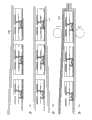
根据本实施例的层压系统具有:传送装置11,用于传送提供有多个薄膜集成电路13的衬底12;用第一薄片构件18缠绕的第一供应辊14;提供有辊16的第一剥离装置51,用于将薄膜集成电路13结合到第一薄片构件18,以从衬底12上剥离薄膜集成电路13;用第二薄片构件19缠绕的第二供应辊15;提供有辊24、28的第二剥离装置52,用于将薄膜集成电路13结合到第二薄片构件19,以从第一薄片构件18剥离薄膜集成电路13;用于收集第一薄片构件18的接收辊21;用于供应第三薄片构件23的第三供应辊22;密封装置17,用于用第二薄片构件19和第三薄片构件23密封薄膜集成电路13;和用于缠绕密封的薄膜集成电路13的接收辊20。The laminating system according to the present embodiment has: a transport device 11 for transporting a
在图1示出的系统中,从第一供应辊14供应的第一薄片构件18结合到由传送装置11传送的衬底12上方的薄膜集成电路13,以用提供有辊16的第一剥离装置15从衬底12剥离薄膜集成电路13。其后,剥离的薄膜集成电路13结合到第一薄片构件18,传过辊28。从第二供应辊15供应的第二薄片构件19传过辊24。In the system shown in FIG. 1 , a
第二薄片构件19与结合到第一薄片构件18的传送的薄膜集成电路13的相对侧粘合,以通过提供有辊24、28的第二剥离装置52将薄膜集成电路13从第一薄片构件18剥离。在将与第一薄片构件18粘合的薄膜集成电路13结合到第二薄片构件19时,进行加压处理和热处理中的一种或两种。其后,剥离的薄膜集成电路13结合到第二薄片构件19,并传过密封装置17。此外,从第三供应辊22供应的第三薄片构件23传过密封装置17。The
密封装置17将与结合到第二薄片构件19的传送薄膜集成电路13侧相对的一侧(与结合到第二薄片19的侧边相对的一侧)结合到第三薄片构件23。同时,进行加压处理和热处理的一种或两种。其后,密封的薄膜集成电路13传过接收辊20,并绕接收辊20缠绕。The sealing
在图1示出的层压系统中,如上所述,第一薄片构件18从第一供应辊供应,并顺序地传过包含于第一剥离装置中的辊28和辊16,然后,由接收辊21收集。第一供座辊14和辊16、28向相同的方向旋转。第二薄片构件19从第二供应辊15供应,并顺序地传过包括于第二剥离装置中的辊24和包括于密封装置17中的辊25,然后,由接收辊20收集。第二供应辊15和辊24、25向相同的方向旋转。第三薄片构件23从第三供应辊22供应,并传过包括于密封装置17中的辊26,然后,由接收辊20收集。第三供应辊22和辊26向相同的方向旋转。In the lamination system shown in FIG. 1, as described above, the
传送装置11传送提供有多个薄膜集成电路13的衬底12。在图1中,传送装置11具有辊27。通过旋转辊27传送衬底12。传送装置11可以具有任何结构,只要其能够传送衬底12。例如,带式运送机、多个辊、机械臂等可用作传送装置11。机械臂传送衬底12或提供有衬底12的台架。此外,传送装置11根据第一薄片构件18的传送速度以预定的速度传送衬底12。The transfer device 11 transfers the
第一薄片构件18、第二薄片构件19和第三薄片构件23分别绕第一供应辊14、第二供应辊15和第三供应辊22缠绕。通过以预定的速度旋转第一供应辊14,第一薄片构件18朝着包括于第二剥离装置中的辊28以预定的速度移动。通过以预定的速度旋转第二供应辊15和第三供应辊22,第二薄片构件19和第三薄片构件23的每个都朝着密封装置17以预定的速度移动。第一供应辊14、第二供应辊15和第三供应辊22为圆柱状,并由树脂材料、金属材料、橡胶材料等制成。The
第一薄片构件18由柔性膜形成,并且具有至少一个带有粘附性质的表面。具体地,通过在用作例如聚酯的基本材料的基膜上提供粘合剂,来制备该粘接表面。作为粘合剂,可以使用树脂材料或包含丙烯酸树脂的合成橡胶材料等。此外,在将提供在衬底上方的薄膜集成电路结合到第一薄片构件之后,为了将薄膜集成电路再次结合到第二薄片构件,以从薄膜集成电路上剥离第一薄片构件,优选使用具有弱粘合力(优选,0.01到1.0N,更优选,0.05到0.75N,更优选,0.15到0.5N)的膜作第一薄片构件18。粘合剂的厚度可以为1到100μm,优选5到50μm,更优选10到30μm。优选,为了在处理中容易操作,由具有10μm到1mm,优选25到200μm、更优选50到100μm厚度的聚酯膜等形成基膜。The
作为第一薄片构件,除了前述的材料外,还可以使用UV(紫外线)剥离膜、热剥离膜等。通过在基膜上方形成由通过UV照射而失去其粘合力的树脂材料制成的粘合层,来制备UV剥离膜。通过在基膜上方形成由通过加热而失去其粘合力的树脂材料制成的粘合层,来制备热剥离膜。As the first sheet member, in addition to the aforementioned materials, a UV (ultraviolet ray) release film, a thermal release film, or the like can be used. A UV release film is prepared by forming an adhesive layer made of a resin material that loses its adhesive force by UV irradiation over a base film. A thermal release film is prepared by forming an adhesive layer made of a resin material that loses its adhesive force by heating over a base film.
在通过隔离物保护粘接层的表面的情况下,如图1所示提供隔离物接收辊30,以在使用中移除隔离物29。此外,经受抗静电处理用作基本材料的基膜可以用作隔离物。由聚酯等制成的膜或纸形成隔离物。隔离物优选由聚对苯二甲酸乙二醇酯等制成的膜形成,因为这在图案化时可以没有纸屑。In the case where the surface of the adhesive layer is protected by a spacer, a
第二薄片构件19和第三薄片构件23由柔性膜形成,例如,层压膜、由纤维材料制成的纸等。层压膜意指通常能够用于层压处理的膜。由例如聚丙烯、聚苯乙烯、聚酯、乙烯树脂、聚氟乙烯、氯乙烯、甲基丙烯酸甲酯、尼龙、聚碳酸酯等的材料制成该层压膜,并且层压膜的表面可以经受例如压花的加工处理。The
在本实施例中,优选用热熔性粘合剂密封该薄膜集成电路。该热熔性粘合剂是不包含水或助熔材料的化学物质,其由室温下为固体的非挥发热塑性材料制成,并且其通过在熔化状态被涂附并被冷却和物品粘合在一起。该热熔性粘合剂具有容易松开、无污染、安全、干净、节省能源和低成本的优点。In this embodiment, the thin film integrated circuit is preferably sealed with a hot melt adhesive. The hot melt adhesive is a chemical substance that does not contain water or fluxing materials, it is made of a non-volatile thermoplastic material that is solid at room temperature, and it is applied in a molten state and is cooled and the object is bonded to the Together. The hot-melt adhesive has the advantages of easy loosening, no pollution, safety, cleanliness, energy saving and low cost.
由于该热熔性粘合剂在常温为固体,所以可以使用预先形成膜或纤维的热熔性粘合剂,或通过在由聚酯等制成的基膜上方形成粘合剂层而形成膜的热熔性粘合剂。这里,使用通过在由聚对苯二甲酸乙二醇酯制成的基膜上方形成热熔膜而制备的薄片构件。该热熔膜由具有比基膜的软化点低的软化点的树脂制成,并且在施加热以粘合时熔化为橡胶态,且在冷却时变硬。作为该热熔膜,可以使用主要包含例如乙烯乙酸乙烯酯共聚物(ethylene-vinyl acetate copolymer)(EVA)系列、聚酯系列、聚酰胺系列、热塑性弹性体系列、聚烯烃系列等的膜。Since this hot-melt adhesive is solid at normal temperature, it is possible to use a hot-melt adhesive that has previously formed a film or fiber, or to form a film by forming an adhesive layer over a base film made of polyester or the like of hot melt adhesives. Here, a sheet member prepared by forming a hot-melt film over a base film made of polyethylene terephthalate was used. The hot-melt film is made of a resin having a softening point lower than that of the base film, and melts into a rubbery state when heat is applied for bonding, and hardens when cooled. As the hot-melt film, films mainly including, for example, ethylene-vinyl acetate copolymer (EVA) series, polyester series, polyamide series, thermoplastic elastomer series, polyolefin series, etc. can be used.
第二薄片构件19和第三薄片构件23的一个或两个可以具有一个粘接表面。可以通过用热固性树脂、紫外线固化树脂、环氧树脂粘合剂、光固化粘合剂、湿气固化粘合剂或树脂添加剂涂敷第二薄片构件19和第三薄片构件23的一个或两个的任一个表面,来制备该粘附表面。One or both of the
第二薄片构件19和第三薄片构件23的一个或两个可以具有透光性。为了保护要被密封的薄膜集成电路13,通过带静电,可以用导电材料涂敷第二薄片构件19和第三薄片构件23的一个或两个。第二薄片构件19和第三薄片构件23的一个或两个可以用主要包含碳(金刚石类碳膜)或例如氧化铟锡(ITO)的导电材料的薄膜涂敷,作为保护膜。One or both of the
第一剥离装置51至少具有辊16,将薄膜集成电路13的任一个表面粘合第一薄片构件18的任一个表面,以从衬底12剥离薄膜集成电路13。通过旋转辊16,将薄膜集成电路13结合到第一薄片构件18,以从衬底12剥离。因此,提供辊16,使其与衬底12的上面提供薄膜集成电路13的一侧相对。此外,辊16为柱状,且由树脂材料、金属材料、橡胶材料等,优选软性材料制成。First peeling
第二剥离装置52至少具有彼此相对的辊24、28,以将薄膜集成电路13结合到第二薄片构件19的任一表面,以从第一薄片构件18剥离薄膜集成电路13。在那种情况下,薄膜集成电路13结合到由第二供应辊15供应并传过辊24的第二薄片构件19;同时,当第二薄片构件19传过辊24、28时,通过利用辊24、28的一个或两个进行加压处理或加热处理的一种或两种。The
根据这种处理,将与第一薄片18粘合的薄膜集成电路13结合到第二薄片构件19。作为热处理,可以使用任何方法,只要其能供应热能。例如,可以使用暖和的介质,例如烤箱、加热金属丝或油的加热器;火印;热头(thermal head);激光;红外线闪光;加热铁笔等。此外,辊24、28都为柱状,且由树脂材料、金属材料、橡胶材料等、优选软性材料制成。According to this process, the thin film integrated
当在薄膜集成电路13的第二表面结合到第二薄片构件19的薄膜集成电路13向密封装置17移动时,密封装置17将第三薄片构件23结合到薄膜集成电路13的第一表面,同时,用第二薄片构件19和第三薄片构件23密封薄膜集成电路13。密封装置17具有彼此相对的辊25、26。薄膜集成电路13的另一个表面结合到由第三供应辊22供应的第三薄片构件23,并传过辊26,同时,当第三薄片构件23通过辊25、26之间时,利用辊25、26进行加压处理和加热处理的一种或两种。根据该处理,薄膜集成电路13用第二薄片构件19和第三薄片构件23密封。When the thin film integrated
组成密封装置17的辊25、26的任一个或两个具有加热装置。作为加热装置,可以使用暖和的介质,例如烤箱、加热导线或油的加热器;火印;热头;激光;红外线闪光;加热铁笔等。根据辊24、第二供应辊15和第三辊22的转速,辊25、26以预定的速度旋转。辊25、26都为柱状,且由树脂材料、金属材料、橡胶材料等、优选软性材料制成。Either or both of the
接收辊20是用于缠绕和收集用第二薄片构件19和第三薄片构件23密封的薄膜集成电路13。根据辊25、26的转速,接收辊20以预定的速度旋转。辊20为柱状,且由树脂材料、金属材料、橡胶材料等、优选软性材料制成。The receiving
如上所述,通过第一到第三供应辊14、15和21,辊16、24、28、25和26,以及接收辊20的旋转,可以连续地剥离、密封和收集提供在衬底12上的多个薄膜集成电路13。在图1中示出的系统具有高的生产率,并可以提高制造效率。As described above, by the rotation of the first to third supply rolls 14, 15, and 21, rolls 16, 24, 28, 25, and 26, and the receiving
参考图2说明具有与前述的层压系统不同形式的层压系统。A lamination system having a different form from the foregoing lamination system is explained with reference to FIG. 2 .
图2中说明的层压系统具有用于衬底12的固定和移动装置33、用于从衬底12的一个表面上剥离薄膜集成电路13的第一剥离装置51、用第一薄片构件18缠绕的第一供应辊14、用第二薄片构件19缠绕的第二供应辊15、用于从第一薄片构件18剥离薄膜集成电路13并将薄膜集成电路13结合到第二薄片构件19的第二剥离装置52、用于在第二薄片构件19和第三薄片构件23之间密封薄膜集成电路13的密封装置17、和用于收集密封的薄膜集成电路13的接收辊20。图2示出的结构是在图1中新加入了固定和移动装置33。The laminating system illustrated in FIG. 2 has a fixing and moving device 33 for a
在图2示出的系统中,从第一供应辊14供应的和传过辊16的第一薄片构件18通过固定与移动装置33与衬底12粘合。因此,薄膜集成电路13通过提供有辊16的第一剥离装置51结合到第一薄片构件18,以从衬底12剥离。与剥离的薄膜集成电路13粘合的第一薄片构件18向辊28移动。此外,从第二供应辊15供应的第二薄片构件19向辊24移动。然后,如图1所示密封薄膜集成电路13。In the system shown in FIG. 2 , the
固定和移动装置33用于固定衬底12,以便上面提供有薄膜集成电路13的衬底12的表面(在下文中,任一表面)相对第一薄片构件18放置,并用于移动衬底12,以将薄膜集成电路13结合到第一薄片构件18。通过移动固定和移动装置33移动衬底12。如图2所示,一个接一个处理衬底12的装置或由圆柱形物体或例如矩形物体的多面体组成的装置可以用作固定和移动装置33。在使用圆柱体或多面体固定和移动装置33的情况下,衬底12被固定在固定和移动装置33的一侧,以通过旋转圆柱体或多面体固定和移动装置33来移动衬底12。The fixing and moving means 33 are used to fix the
如上所述,在图2示出的层压系统中,通过旋转固定和移动装置33、第一到第三供应辊、辊16、24、28、25和26、以及接收辊20,连续地剥离、密封和收集薄膜集成电路13。因此,通过利用图2示出的层压系统,可以提高大量生产率和制造效率。As described above, in the lamination system shown in FIG. , sealing and collecting the thin film integrated
参考图3说明具有与前述的层压系统不同形式的层压系统。A lamination system having a different form from the foregoing lamination system is explained with reference to FIG. 3 .
图3示出的层压系统,具有用于传送衬底12的传送装置11;用于从衬底12的任一表面剥离薄膜集成电路13的第一剥离装置51;用第一薄片构件18缠绕的第一供应辊14;用第二薄片构件19缠绕的第二供应辊15;用于从第一薄片构件18剥离薄膜集成电路13并且将剥离的薄膜集成电路结合到第二薄片构件19的第二剥离装置52;用于用第二薄片构件19和树脂55密封薄膜集成电路13的密封装置17,该树脂55是在被加热的状态下挤到薄膜集成电路13的与第二薄片构件19粘合的表面相对的表面上的;和用于缠绕密封的薄膜集成电路13的接收辊20。图3示出的结构是除了用染料54和树脂55代替第三供应辊22和第三薄片构件23之外如图1所示的结构。The laminating system shown in Fig. 3 has the conveying device 11 for conveying the
图3示出的系统可以根据图1示出的进行处理,一直到通过第一薄片构件18剥离提供在衬底12上方的薄膜集成电路13,将与第一薄片构件18粘合的薄膜集成电路13结合到第二薄片构件19,并将与第二薄片构件19粘合的薄膜集成电路13向密封装置17移动。其后,在图3中,加热到熔化的树脂55从染料54挤到第一表面上(与和第二薄片构件粘合的第二表面相对的表面)。然后,冷却引入到蜷曲辊(crimping roller)56和冷却辊57之间的第二薄片构件19和树脂55,同时通过蜷曲辊56和冷却辊57施加压力,以将树脂55结合到薄膜集成电路13的第一表面,同时,用第二薄片构件19和树脂55密封薄膜集成电路13。最后,密封的薄膜集成电路13向接收辊20移动以被缠绕,并由接收辊20收集。The system shown in FIG. 3 can be processed according to that shown in FIG. 1 until the thin film integrated
在图3示出的层压系统的结构中,使用热塑性树脂作为树脂55。具有低软化点的热塑性树脂优选用作树脂55。例如,可以指定聚烯烃树脂,例如聚乙烯、聚丙烯或聚甲基丙烯酸甲酯戊烯(polymethylpentene);乙烯共聚物,例如氯乙烯、醋酸乙烯、聚氯乙烯-乙酸乙烯酯共聚物、乙烯乙酸乙烯共聚物、偏氯乙烯、聚乙烯醇缩丁醛或聚乙烯醇;丙烯酸树脂;聚酯树脂;聚氨酯树脂;纤维素树脂,例如纤维素、醋酸纤维素、乙酸丁酸纤维素、醋酸纤维素丙酸酯或乙基纤维素;苯乙烯树脂,例如聚苯乙烯或丙烯腈-苯乙烯共聚物。树脂55可以是从染料54挤出的单层,可选地,也可以是从染料54一起挤出的两层或多层。此外,可以使用前述材料的任何一种作为第一薄片构件18或第二薄片构件19。In the structure of the lamination system shown in FIG. 3 , a thermoplastic resin is used as the
如上所述,根据图3示出的层压系统,通过旋转传送装置11、第一和第二供应辊14、15、辊16、24和28、蜷曲辊56、冷却辊57和接收辊20;连续地剥离、密封和收集提供在衬底12上方的多个薄膜集成电路13。因此,在图3中示出的系统可以提高大批量生产率和制造效率。As mentioned above, according to the lamination system shown in FIG. 3, through the rotating conveyor 11, the first and second supply rolls 14, 15, rolls 16, 24 and 28, crimping
然后,参考图4说明层压系统的全部结构。这里,引用包括图1示出的结构的层压系统的结构作为说明的例子。Then, the overall structure of the lamination system will be explained with reference to FIG. 4 . Here, the structure of a lamination system including the structure shown in FIG. 1 is cited as an illustrative example.
盒子41是用于提供衬底的盒子,其中放置着提供有多个薄膜集成电路13的衬底12。盒子42是用于收集衬底的盒子,其收集与薄膜集成电路13分开之后的衬底12。在盒子41和42之间提供多个辊43到45,作为传送装置。通过辊43到45的旋转传送衬底12。其后,如上所述,薄膜集成电路13被剥离和密封,且通过切割装置46切割密封的薄膜集成电路13。切割装置46使用切片机、划片机、激光照射机(CO2激光照射机)等。根据前述的工艺完成密封的薄膜集成电路13。The cassette 41 is a cassette for supplying a substrate, and the
在图1到3示出的前述结构中,提供在衬底12上方的薄膜集成电路13包括由多个元件组成的元件组和用作天线的导电层。然而,本发明不限于这种结构。In the aforementioned structures shown in FIGS. 1 to 3, the thin film integrated
提供在衬底12上方的薄膜集成电路13可以仅包括元件组。当薄膜集成电路13结合到第二薄片构件19或第三薄片构件23时,用作天线的导电层粘贴到第二薄片构件19或第三薄片构件23上,且多个包括于薄膜集成电路13的元件可以连接到导电层。Thin film integrated
实施例2Example 2
在本实施例中,在下文说明IC薄片(也称作IC膜、薄片构件或膜构件)的结构。In this embodiment, the structure of an IC chip (also referred to as an IC film, a sheet member, or a film member) is explained below.
如图5所示,IC薄片是通过在两个薄片构件19和23之间插入以密封薄膜集成电路13中每一个所形成的薄片。通过如实施例1所示在第二薄片构件19和第三薄片构件23之间插入以密封多个薄膜集成电路来获得IC薄片。As shown in FIG. 5 , the IC chip is a chip formed by interposing between two
薄膜集成电路13的每一个都具有多个元件和用作天线的导电层。而且,通过有效地剥离提供在衬底上方的薄膜集成电路薄膜集成电路的每一个都可以有规则地布置成薄片(图5A)。而且,一个IC薄片可在辊中卷起或自身折进去(图5B)。Each of the thin film integrated
如上所述,容易载运包括用一对薄片构件密封的多个薄膜集成电路13的薄片状IC薄片。尤其是,IC薄片在制造大量薄膜集成电路13的情况下载运是有效的。切割成片的多个薄膜集成电路13具有处理的困难。因为IC薄片形成为薄片状,所以根据本实施例的IC薄片的处理容易。另外,根据本实施例的IC薄片可以保护薄膜集成电路13不受损坏和破坏。当想从IC薄片单独地移除薄膜集成电路13时,可通过切片机、划片机、激光照射机(CO2激光照射机)等切割薄膜集成电路13。As described above, it is easy to carry a chip-shaped IC chip including a plurality of thin film integrated
本实施例可以与前述实施例自由地组合。This embodiment can be freely combined with the foregoing embodiments.
实施例3Example 3
在本实施例中,在下文说明IC薄片卷轴的结构。In this embodiment, the structure of the IC chip reel is explained below.
如图6所示,IC薄片卷是通过将薄片构件卷于轴上形成的。具体地,IC薄片卷轴是通过将插入以密封在两个薄片构件19和23之间的多个薄膜集成电路13卷于轴上成为卷轴而形成的。如实施例1中所描述的,IC薄片卷轴是通过将卷轴卷于轴上收集用第二薄片构件19和第三薄片构件23密封的薄片状的多个薄膜集成电路13来获得的。薄膜集成电路13的每一个具有多个元件和用作天线的导电层。而且,薄膜集成电路13的每一个有规则地布置。As shown in FIG. 6, an IC wafer roll is formed by rolling a wafer member on a reel. Specifically, the IC sheet reel is formed by winding a plurality of thin film integrated
如上所述,容易载运通过将用一对薄片构件密封的薄膜集成电路13卷于轴上所形成的IC薄片的卷轴。尤其是,IC薄片卷轴在制造大量薄膜集成电路13的情况下载运是有效的。通常,切割成片的多个薄膜集成电路13具有处理的困难。因为IC薄片被卷成卷轴,所以根据本实施例的IC薄片卷轴的处理是容易的。例如,可以在如图6B所示的状态使用薄膜集成电路13。另外,根据本实施例的IC薄片可以通过使用如上所述的方式保护薄膜集成电路13不被损坏和破坏。As described above, it is easy to carry the reel of the IC sheet formed by winding the thin film integrated
本实施例可以与前述实施例自由地组合。This embodiment can be freely combined with the foregoing embodiments.
实施例4Example 4
在本实施例中,在下文参考各图说明根据本发明制造IC芯片的方法。In this embodiment, a method of manufacturing an IC chip according to the present invention is explained below with reference to the figures.
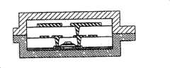
在衬底100上形成剥离层101(图7A)。作为衬底100,可以使用玻璃衬底例如硼硅酸钡玻璃或硼硅酸铝玻璃、石英衬底、陶瓷衬底等。可以使用上面形成绝缘膜的半导体衬底,例如包括不锈钢的金属衬底或硅衬底。由合成树脂例如具有柔性的塑料制成的衬底一般具有比前述衬底低的容许温度限制;然而仅可以在制造工艺中耐受处理温度的情况下使用。可通过抛光例如CMP方法使衬底100的表面平滑。当利用硅衬底时,不需要提供剥离层101。A
通过溅射方法、等离子体CVD等形成含硅的层来形成剥离层101。含硅的层对应于包括硅的非晶半导体膜、为非晶态和结晶态的混合状态的半非晶半导体膜、结晶半导体膜等。作为剥离层101,可以使用含金属的膜。例如,作为金属膜和金属氧化物膜,可以分别形成W和WOx、Mo和MoOx、Nb和NbOx、Ti和TiOx(x=2、3)等。这里,剥离层101全部形成在衬底100上方;可选地,其选择性地形成在衬底100上。The
在本实施例中在衬底100上直接形成剥离层101。可以在衬底100和剥离层101之间形成基膜。该基膜可以是含氧或氮的绝缘膜例如氧化硅(SiOx)、氮化硅(SiNx)、氮氧化硅(SiOxNy)(x>y)或氧化氮化硅(SiNxOy)(x<y)(x、y=1、2......)的单层结构或叠层结构。尤其是,在害怕衬底被污染的情况下,优选在衬底100和剥离层101之间形成基膜。In this embodiment, the
在剥离层101上方形成绝缘膜102作为基膜。可以形成绝缘膜102以具有单层结构或叠层结构。例如,可形成绝缘膜以具有由三层例如氧化硅膜作为第一绝缘膜、氧化氮化硅膜作为第二绝缘膜和氮氧化硅膜作为第三绝缘膜组成的叠层结构。An insulating
在绝缘膜102上方形成元件组103。作为元件组103,例如,一个或多个薄膜晶体管、电容元件、电阻元件、二极管等。图7示例了具有GOLD结构的薄膜晶体管形成为元件组103;然而,可通过在栅电极的侧面形成侧壁以具有LDD结构来形成薄膜晶体管。The
形成绝缘膜104以覆盖元件组103。在绝缘膜104上方形成绝缘膜105。然后,在绝缘膜105上方形成用作天线的导电层106。其后,在导电层106上方形成用作保护膜的绝缘膜107。在进行前述工艺之后,完全地制造包括元件组103和导电层106的薄膜集成电路108。An insulating
对于绝缘膜104、105和107可以使用无机绝缘膜或有机绝缘膜。作为无机绝缘膜,通过CVD方法形成氧化硅膜或氮氧化硅膜或由SOG(玻璃上旋涂)方法涂敷的氧化硅膜。作为有机绝缘膜,可以使用由聚酰亚胺、聚酰胺、BCB(苯环丁烯)、丙烯酸、正型光敏有机树脂、负型有机树脂等制成的膜。可以使用丙烯酸膜和氮氧化硅膜的叠层结构。An inorganic insulating film or an organic insulating film can be used for the insulating
绝缘膜104、105和107可以通过硅氧烷树脂形成。硅氧烷树脂对应于包括Si-O-Si键的树脂。硅氧烷由通过硅(Si)和氧(O)的键形成的骨架组成,其中作为取代基包括至少包含氢的有机基团(例如烷基基团或芳烃)。可选地,可使用氟代基团作为取代基。而且可选地,作为取代基可使用至少包含氢的有机基团和氟代基团。The insulating
硅氧烷树脂可以分成硅石玻璃、烷基硅氧烷聚合物、烷基倍半硅氧烷(alkylsilsesquioxane)聚合物、氢化倍半硅氧烷(hydrogenatedsilsesquioxane)聚合物、氢化烷基硅氧烷聚合物等。可以通过包含具有Si-N键的聚合物(聚硅氮烷)的材料形成层间绝缘膜。Silicone resin can be divided into silica glass, alkylsiloxane polymer, alkylsilsesquioxane polymer, hydrogenatedsilsesquioxane polymer, hydrogenated alkylsiloxane polymer wait. The interlayer insulating film can be formed by a material including a polymer (polysilazane) having a Si—N bond.
形成开口部分111、112以便在薄膜集成电路108之间暴露出剥离层101(图7B)。利用掩模通过蚀刻或切片形成开口111、112。图10A是示出这种状态的顶视图。图7A至7C中的截面图对应于沿着线A-B得到的图10A。Opening
将用于移除剥离层101的蚀刻剂引入到开口部分111、112中,以逐渐移除除了剥离层113至115的部分之外的剥离层(图7C和10B)。作为蚀刻剂,使用含卤素氟化物的气体或液体。例如,作为卤素氟化物使用三氟化卤素(ClF3)。An etchant for removing the
如上所述,在该工艺中没有完全移除剥离层101以留下位于薄膜集成电路108下面的剥离层113至115的部分。因此,可以防止薄膜集成电路108分散被散开,其导致甚至在剥离之后保持如在剥离之前的布置。在不害怕分散薄膜集成电路108的情况下,可以在完全地移除剥离层101之后进行剥离。As described above, the lift-
将薄膜集成电路108的第一表面结合到第一薄片构件116。因此,从衬底100剥离薄膜集成电路108(图8A)。如上所述,在从衬底100物理地剥离薄膜集成电路108同时留下剥离层101的部分113至115的情况下,优选在剥离层101上方形成金属膜。例如,在利用W或Mo作为剥离层的情况下,在W或Mo上方形成氧化硅膜,并且通过热处理等在W或Mo上方分别形成WOx或MoOx。通过形成金属氧化膜,剥离层变得容易从氧化硅膜剥离,并且衬底和薄膜集成电路可以容易地分开,而不完全移除剥离层。而且,由柔性膜形成第一薄片构件116,并且将粘合剂至少提供给与薄膜集成电路108接触的第一薄片构件116的表面。例如,可以使用通过在由聚酯等制成的基膜上方形成提供具有含丙烯酸树脂的不良粘合性的粘合剂的膜所形成的膜。The first surface of the thin film integrated
将薄膜集成电路108的第二表面结合到第二薄片构件117,以从第一薄片构件117剥离薄膜集成电路108(图8B)。The second surface of the thin film integrated
将第三薄片构件118结合到与第二薄片构件117结合的表面相对的薄膜集成电路108的表面,同时,用第二薄片构件117和第三薄片构件118密封薄膜集成电路108(图8C)。因此,用第二薄片构件117和第三薄片构件118密封薄膜集成电路108(图8C)。第二薄片构件117和第三薄片构件118通过例如层压膜的柔性膜形成。具体地,可以使用在例如聚酯的基膜上方形成的热熔膜。当将第二薄片构件117和第三薄片构件118结合到薄膜集成电路108时进行加压处理和加热处理之一或二者,这使得能够在短时间内结合薄膜集成电路108。The
通过切片、划线或激光切割法在薄膜集成电路108之间选择性地切割第二薄片构件117和第三薄片构件118。因此,完全地制造密封的IC芯片(图9A和9B)。The
通过前述工艺完成的密封IC芯片具有5mm见方(25mm2)或更少、优选0.3mm见方(0.09mm2)至4mm见方(16mm2)的尺寸。The sealed IC chip completed by the foregoing process has a size of 5 mm square (25 mm2 ) or less, preferably 0.3 mm square (0.09 mm2 ) to 4 mm square (16 mm2 ).
由于在不使用硅衬底的情况下根据本发明的芯片使用在绝缘衬底上方形成的薄膜集成电路,所以对与由圆形硅衬底形成的芯片不同的母板衬底的形状不存在限制。因此,可以提高芯片的生产率,并可以实现批量生产。剥离的衬底可在上述工艺中重复使用。可以减少利用例如玻璃的衬底制造薄膜集成电路的成本。例如,不管其在平面和高耐热性的优点,存在石英衬底的高的最初成本的问题。甚至在利用比玻璃衬底花费更多的石英衬底的情况下,重复使用衬底也会引起成本减少。在本实施例中,在石英衬底上方形成薄膜集成电路,并剥离薄膜集成电路,然后重复使用石英衬底。因此,可以以低成本制造具有较高特性的薄膜集成电路。Since the chip according to the present invention uses a thin film integrated circuit formed over an insulating substrate without using a silicon substrate, there is no restriction on the shape of the mother substrate different from a chip formed of a circular silicon substrate . Therefore, the productivity of chips can be improved, and mass production can be realized. The peeled substrate can be reused in the above process. The cost of manufacturing a thin film integrated circuit using a substrate such as glass can be reduced. For example, despite its advantages in planarity and high heat resistance, there is a problem of high initial cost of the quartz substrate. Even with the use of quartz substrates, which cost more than glass substrates, reusing the substrates results in a cost reduction. In this embodiment, a thin film integrated circuit is formed over a quartz substrate, and the thin film integrated circuit is peeled off, and then the quartz substrate is reused. Therefore, thin film integrated circuits with higher characteristics can be manufactured at low cost.
由于在本实施例中说明的IC芯片使用具有0.2μm或更少、一般40至170nm、优选50至150nm厚度的半导体膜作为有源区,所以形成极薄状的IC芯片。结果,由于在装配到物品的状态很难认识到薄膜集成电路,所以可以防止损害。而且,不害怕无线电波吸收,并且与由硅衬底形成的IC芯片不同可以接收高敏感信号。不具有硅衬底的薄膜集成电路具有透光性质。因此,薄膜集成电路可以用于各种物品。例如,薄膜集成电路可以装配到物品的印刷表面,其不会减损物品的设计。Since the IC chip described in this embodiment uses a semiconductor film having a thickness of 0.2 μm or less, generally 40 to 170 nm, preferably 50 to 150 nm, as an active region, an extremely thin IC chip is formed. As a result, damage can be prevented since the thin film integrated circuit is hardly recognized in a state of being mounted on an article. Also, there is no fear of radio wave absorption, and highly sensitive signals can be received unlike IC chips formed of silicon substrates. Thin film integrated circuits that do not have a silicon substrate have light-transmitting properties. Therefore, thin film integrated circuits can be used for various articles. For example, thin film integrated circuits can be fitted to the printed surface of an article without detracting from the design of the article.
本实施例可以与前述实施例自由地组合。This embodiment can be freely combined with the foregoing embodiments.
实例1Example 1
在该实例中,参考图15A至16B说明在前述实施例中说明的制造IC芯片的方法中制造栅电极的方法。如果没有另外指定,则可以通过使用与实施例中描述的相同的材料制造栅电极。In this example, a method of manufacturing a gate electrode in the method of manufacturing an IC chip explained in the foregoing embodiments is explained with reference to FIGS. 15A to 16B . If not specified otherwise, the gate electrode can be fabricated by using the same material as described in the embodiment.
首先,在衬底200上方形成剥离层201以经由绝缘层202、203提供半导体膜211、212。此外在半导体膜211、212上方形成栅绝缘膜213。其后,在栅绝缘膜213上方叠置第一导电层951和第二导电层952。在该实例中,对于第一导电层使用氮化钽(TaN),并且对于第二导电层使用钨(W)。可利用氮气氛下的钽靶通过溅射方法形成TaN膜。可利用钨靶通过溅射方法形成W膜。First, a lift-
在该实例中,第一导电层951由TaN制成,第二导电层952由W制成。然而,用于第一导电层951和第二导电层952的材料不限制于TaN和W。可以使用选自Ta、W、Ti、Mo、Al、Cu、Cr和Nd的元素;合金材料或化合物材料,其每个都主要包含前述元素。可选地,如由多晶硅膜为代表的半导体膜掺杂有例如磷的杂质元素。而且可选地,可以使用AgPdCu合金。可以适当地选择导电层的组合。可形成第一导电层951以具有从20到100nm范围的厚度。第二导电层952可形成以具有从100到400nm范围的厚度。在该实例中,形成导电层以具有两层的叠层结构。可选地,可形成单层的导电层,或可形成导电层以具有三层或更多层的叠层结构。In this example, the first
然后,通过光刻法或液滴排放法在第二导电层952上方选择性地形成抗蚀剂953(图15A)。其后,通过已知的蚀刻处理例如O2(氧)等离子体蚀刻抗蚀剂953来减小抗蚀剂953的尺寸(图15B)。当利用减小的抗蚀剂954作掩模蚀刻第一导电层951和第二导电层952时,可以形成具有进一步减小宽度的栅电极。即,可以形成比通过利用由一般图案化获得的抗蚀剂953形成的栅电极具有更小宽度的栅电极。以这种方式,通过减小栅电极结构的尺寸来减小沟道形成区的宽度。因此,可以高速工作。Then, a resist 953 is selectively formed over the second
参考图16A和16B说明与图15A和15B中所示的栅电极不同的栅电极的制造方法。A method of manufacturing a gate electrode different from that shown in FIGS. 15A and 15B will be described with reference to FIGS. 16A and 16B .
如图15A所示,叠置剥离层201、绝缘膜202、203、半导体膜211、212、栅绝缘膜213、第一导电层951和第二导电层952。然后,选择性地形成抗蚀剂953。然后,利用抗蚀剂953作为掩模蚀刻第一导电层951和第二导电层952(图16A)。根据该工艺,通过第一导电层951和第二导电层952形成栅电极956。其后,通过蚀刻法蚀刻栅电极956。由于在栅电极956上方提供抗蚀剂953,所以蚀刻栅电极956的侧面;因此,可以如图16B所示形成具有比栅电极956小宽度的栅电极957。As shown in FIG. 15A , the
根据在该实例中说明的制造方法,可以制造具有超过通过光刻法等图案化限度的尺寸的小栅电极。通过最小化栅电极,可以提供小的元件结构。因此,可以形成更多元件,并且可以形成具有高性能的电路。而且,在形成薄膜集成电路以具有与在前相同数量元件的情况下,可以小型化薄膜集成电路(IC芯片等)。可以组合图15A和15B中所示的方法和图16A和16B中所示的方法来形成更小的栅电极。According to the manufacturing method described in this example, a small gate electrode having a size exceeding the limit of patterning by photolithography or the like can be manufactured. By minimizing the gate electrode, a small element structure can be provided. Therefore, more elements can be formed, and a circuit with high performance can be formed. Also, in the case of forming a thin film integrated circuit to have the same number of elements as before, it is possible to miniaturize the thin film integrated circuit (IC chip, etc.). The method shown in FIGS. 15A and 15B and the method shown in FIGS. 16A and 16B can be combined to form a smaller gate electrode.
该实例可以通过自由地组合前述实施例来实施。This example can be implemented by freely combining the foregoing embodiments.
实例2Example 2
在该实例中,参考图14说明与实例1中描述的不同的TFT层102的结构。In this example, the structure of the
图14示出了一种结构,其为加有底电极的图7A中元件结构103的结构。即,如图14所示,结构519包括经由绝缘膜介于底电极513和栅电极214之间的半导体膜311的沟道区。FIG. 14 shows a structure which is the structure of the
可以通过金属或加有一种导电类型杂质的多晶半导体形成底电极513。在使用金属的情况下,可以使用W、Mo、Ti、Ta、Al等。而且,形成用作基底绝缘膜的氮化硅膜514和氮氧化硅膜515。氮化硅膜514和氮氧化硅膜515的材料和叠置顺序不限制于这里描述的那些。The
如上所述,可以使用具有底电极的TFT作为TFT层102的结构。通常,当减小TFT的尺寸和提高用于操作电路的时钟频率时,增加了集成电路的功耗。因此,将偏压施加到底电极的方法在阻止增加功耗方面是有用的。通过改变偏压,可以改变TFT的阈值电压。As described above, a TFT having a bottom electrode can be used as the structure of the
将负偏压施加到n沟道TFT的底电极随着泄漏减小而增加了阈值电压。另一方面,施加正偏压降低了阈值电压,其导致穿过沟道的电流容易流动和TFT以高速度或在低电压下工作。而且,将正偏压施加到p沟道TFT的底电极随着泄漏降低而增加了阈值电压。另一方面,施加负电压降低了阈值电压,其导致穿过沟道的电流容易流动和TFT以高速度或在低电压下工作。通过控制用于施加到底电极的偏压,可以显著地改善集成电路的特性。Applying a negative bias to the bottom electrode of an n-channel TFT increases the threshold voltage as leakage decreases. On the other hand, applying a positive bias lowers the threshold voltage, which results in easy flow of current through the channel and TFT operation at high speed or at low voltage. Also, applying a positive bias to the bottom electrode of a p-channel TFT increases the threshold voltage as leakage decreases. On the other hand, applying a negative voltage lowers the threshold voltage, which causes current to easily flow through the channel and TFT to operate at high speed or at low voltage. By controlling the bias voltage applied to the bottom electrode, the characteristics of the integrated circuit can be significantly improved.
通过平衡n沟道TFT和p沟道TFT的阈值电压与偏压,可以改善集成电路的特性。在那种情况下,为了减小功耗,可以控制用于施加到底电极的偏压和电源电压二者。当电路处于待机模式时,将大的反向偏压施加到底电极。工作时,当负载小时将弱的反向偏压施加到底电极,而当负载大时施加弱的正偏压。偏压的施加能够通过提供控制电路根据电路的工作状态或负载被切换。通过以这种方式控制功耗或TFT性能,可以最大化电路性能。By balancing the threshold voltage and bias voltage of n-channel TFTs and p-channel TFTs, the characteristics of integrated circuits can be improved. In that case, in order to reduce power consumption, both the bias voltage applied to the bottom electrode and the power supply voltage can be controlled. When the circuit is in standby mode, a large reverse bias is applied to the bottom electrode. In operation, a weak reverse bias is applied to the bottom electrode when the load is small, and a weak forward bias is applied when the load is large. The application of the bias voltage can be switched according to the operating state of the circuit or the load by providing a control circuit. By controlling power consumption or TFT performance in this way, circuit performance can be maximized.
该实例可以与前述实施例和实例自由地组合。This example can be freely combined with the foregoing embodiments and examples.
实例3Example 3
在该实例中,说明通过根据本发明的制造方法制造的IC芯片的结构。In this example, the structure of an IC chip manufactured by the manufacturing method according to the present invention is explained.
图11A是一种形式的IC芯片的透视图。附图标记920表示集成电路,921表示天线。天线921电连接至集成电路920。附图标记922表示衬底,923表示盖组件。集成电路920和天线921层夹在衬底922和盖组件923之间。Figure 11A is a perspective view of one form of an IC chip.
图11B示出了在图11A中示出的IC芯片的一种形式动能结构。FIG. 11B shows a form of kinetic energy structure of the IC chip shown in FIG. 11A.
在图11B中,附图标记900表示天线;901,集成电路;903,形成在天线900的端子之间的电容。集成电路901具有解调电路909、调制电路904、整流电路905、微处理器906、存储器907和用于将载荷调制给天线900的开关908。存在一个以上的存储器907。可以使用多个存储器,例如SRAM、闪存、ROM、FRAM(注册商标)等。In FIG. 11B , reference numeral 900 denotes an antenna; 901 , an integrated circuit; 903 , a capacitance formed between terminals of the antenna 900 . The
通过天线900中的电磁感应将从读出器/记录器发出的作为电波的信号转换成交变的电信号。解调电路909解调交变的电信号,以在随后的步骤将它发送到微处理器906。整流电路905通过交变的电信号产生电源电压,以在随后的步骤将它供给微处理器906。微处理器906根据输入信号执行各种运算处理。存储器907存储微处理器906中使用的程序和数据。存储器907可以用作运算处理时的工作区。A signal sent from the reader/writer as an electric wave is converted into an alternating electric signal by electromagnetic induction in the antenna 900 . The
当数据从微处理器906发送到调制电路904时,调制电路904可以控制开关908以根据该数据将负载调制施加到天线900。结果,读出器/记录器可以通过接收供给天线900的负载调制读取来自微处理器906的数据。When data is sent from
IC芯片不总是必须具有微处理器906。信号的传输系统不限制于如图11B所示的前述电磁耦合系统。可以使用电磁系统、微波系统或另一传输系统。An IC chip does not always have to have a
由于具有天线的IC芯片可以传输外部信号,所以IC芯片可以用作无线存储器或无线处理器。Since an IC chip having an antenna can transmit external signals, the IC chip can be used as a wireless memory or a wireless processor.
该实例可以与前述实施例和实例自由地组合。This example can be freely combined with the foregoing embodiments and examples.
实例4Example 4
在该实例中,说明在前述实施例或实例中描述的薄膜集成电路的用法。从衬底剥离的薄膜集成电路可以用作IC芯片210,例如,纸币、硬币、证券、无记名债券、证书(驾驶执照、居民卡等,参考图12A)、包装容器(包装纸、瓶等,参考图12B)、记录媒质例如DVD软件、CD或录像磁带(图12C)、交通工具例如汽车、摩托车或自行车(图12D)、日用品例如包或眼镜(图12E)、食品、服装、消费商品、电器等。电器表示液晶显示器件、EL显示器件、电视设备(称作电视或电视机)、蜂窝电话等。In this example, usage of the thin film integrated circuit described in the foregoing embodiments or examples is explained. The thin film integrated circuit peeled off from the substrate can be used as the
可以通过粘贴到物品的表面上或嵌入物品中将IC芯片固定到物品。例如,可将IC芯片嵌入在书籍的纸张中或由有机树脂制成的包装的有机树脂中。可以通过提供IC芯片到纸币、硬币、证券、无记名债券、证书来防止伪造。通过提供IC芯片给包装容器、记录媒质、日用品、食品、服装、消费商品、电器等,可以使检查系统或在租用商店中使用的系统更有效。可以通过提供IC芯片给交通工具来防止仿制或盗窃。The IC chip can be fixed to the item by being pasted on the surface of the item or embedded in the item. For example, an IC chip can be embedded in the paper of a book or in the organic resin of a package made of organic resin. Counterfeiting can be prevented by providing IC chips to bills, coins, securities, bearer bonds, certificates. By providing IC chips to packaging containers, recording media, daily necessities, food, clothing, consumer goods, electric appliances, etc., an inspection system or a system used in rental shops can be made more effective. Counterfeiting or theft can be prevented by providing IC chips to vehicles.
通过将IC芯片施加到用于商品管理或分发的系统,可以使该系统复杂。例如,如图13A所示,将读出器/记录器295提供给具有显示部分294的便携式端子的侧面的情况和IC芯片296提供给物品297的侧面(图13A)的情况作为实例。在那种情况下,当IC芯片296保持在读出器/记录器295上方时,有关物品297的原料、原产地和分发过程的历史的信息显示在显示部分294上。作为另一实例,在带式运送机旁提供读出器/记录器295的情况下,可以容易地进行提供有IC芯片296的物品297的检查(图13B)。The system can be complicated by applying an IC chip to the system for merchandise management or distribution. For example, as shown in FIG. 13A, the case where the reader/
该实例可以通过与前述实施例和实例自由地组合来实施。This example can be implemented by freely combining with the aforementioned embodiments and examples.
Claims (19)
Applications Claiming Priority (2)
| Application Number | Priority Date | Filing Date | Title |
|---|---|---|---|
| JP2004224789 | 2004-07-30 | ||
| JP224789/2004 | 2004-07-30 |
Publications (2)
| Publication Number | Publication Date |
|---|---|
| CN101002312A CN101002312A (en) | 2007-07-18 |
| CN100530575Ctrue CN100530575C (en) | 2009-08-19 |
Family
ID=35786393
Family Applications (1)
| Application Number | Title | Priority Date | Filing Date |
|---|---|---|---|
| CNB2005800258794AExpired - Fee RelatedCN100530575C (en) | 2004-07-30 | 2005-07-28 | Laminating system, IC sheet, scroll of IC sheet, and method for manufacturing IC chip |
Country Status (4)
| Country | Link |
|---|---|
| US (1) | US9053401B2 (en) |
| KR (1) | KR101254277B1 (en) |
| CN (1) | CN100530575C (en) |
| WO (1) | WO2006011665A1 (en) |
Families Citing this family (55)
| Publication number | Priority date | Publication date | Assignee | Title |
|---|---|---|---|---|
| WO2005119781A1 (en) | 2004-06-02 | 2005-12-15 | Semiconductor Energy Laboratory Co., Ltd. | Laminating system |
| US7591863B2 (en)* | 2004-07-16 | 2009-09-22 | Semiconductor Energy Laboratory Co., Ltd. | Laminating system, IC sheet, roll of IC sheet, and method for manufacturing IC chip |
| US8153511B2 (en)* | 2005-05-30 | 2012-04-10 | Semiconductor Energy Laboratory Co., Ltd. | Method for manufacturing semiconductor device |
| US7605056B2 (en)* | 2005-05-31 | 2009-10-20 | Semiconductor Energy Laboratory Co., Ltd. | Method of manufacturing a semiconductor device including separation by physical force |
| US7485511B2 (en)* | 2005-06-01 | 2009-02-03 | Semiconductor Energy Laboratory Co., Ltd. | Integrated circuit device and method for manufacturing integrated circuit device |
| US7504317B2 (en) | 2005-12-02 | 2009-03-17 | Semiconductor Energy Laboratory Co., Ltd. | Manufacturing method of semiconductor device |
| US20070183184A1 (en) | 2006-02-03 | 2007-08-09 | Semiconductor Energy Laboratory Ltd. | Apparatus and method for manufacturing semiconductor device |
| WO2007107299A1 (en)* | 2006-03-17 | 2007-09-27 | Polyic Gmbh & Co. Kg | Method for producing an active or passive electronic component, and electronic component |
| US8900970B2 (en) | 2006-04-28 | 2014-12-02 | Semiconductor Energy Laboratory Co., Ltd. | Method for manufacturing a semiconductor device using a flexible substrate |
| US7727809B2 (en)* | 2006-05-31 | 2010-06-01 | Semiconductor Energy Laboratory Co., Ltd. | Attachment method, attachment apparatus, manufacturing method of semiconductor device, and manufacturing apparatus of semiconductor device |
| TWI424499B (en)* | 2006-06-30 | 2014-01-21 | Semiconductor Energy Lab | Method of manufacturing a semiconductor device |
| TWI611565B (en) | 2006-09-29 | 2018-01-11 | 半導體能源研究所股份有限公司 | Semiconductor device manufacturing method |
| US8137417B2 (en) | 2006-09-29 | 2012-03-20 | Semiconductor Energy Laboratory Co., Ltd. | Peeling apparatus and manufacturing apparatus of semiconductor device |
| US8044813B1 (en) | 2006-11-16 | 2011-10-25 | Semiconductor Energy Laboratory Co., Ltd. | Radio field intensity measurement device, and radio field intensity detector and game console using the same |
| JP2008134694A (en)* | 2006-11-27 | 2008-06-12 | Philtech Inc | Rf powder adding method and rf powder added base sheet |
| JP2008135446A (en)* | 2006-11-27 | 2008-06-12 | Philtech Inc | Method of producing rf powder |
| JP2008134695A (en)* | 2006-11-27 | 2008-06-12 | Philtech Inc | Base data management system |
| JP2008135951A (en)* | 2006-11-28 | 2008-06-12 | Philtech Inc | Rf powder particle, rf powder, and substrate containing rf powder |
| JP2008134816A (en)* | 2006-11-28 | 2008-06-12 | Philtech Inc | Rf powder particle, rf powder, and rf powder exciting method |
| JP2008134815A (en)* | 2006-11-28 | 2008-06-12 | Philtech Inc | Rf powder providing method, and liquid containing rf powder |
| JP2008136019A (en)* | 2006-11-29 | 2008-06-12 | Philtech Inc | Magnetic coupling device and reader |
| US8237622B2 (en)* | 2006-12-28 | 2012-08-07 | Philtech Inc. | Base sheet |
| US7968382B2 (en) | 2007-02-02 | 2011-06-28 | Semiconductor Energy Laboratory Co., Ltd. | Method of manufacturing semiconductor device |
| EP2019425A1 (en) | 2007-07-27 | 2009-01-28 | Semiconductor Energy Laboratory Co., Ltd. | Semiconductor device and method for manufacturing the same |
| WO2009148001A1 (en) | 2008-06-06 | 2009-12-10 | Semiconductor Energy Laboratory Co., Ltd. | Method for manufacturing semiconductor device |
| JP5586920B2 (en)* | 2008-11-20 | 2014-09-10 | 株式会社半導体エネルギー研究所 | Method for manufacturing flexible semiconductor device |
| KR20150120376A (en) | 2013-02-20 | 2015-10-27 | 가부시키가이샤 한도오따이 에네루기 켄큐쇼 | Peeling method, semiconductor device, and peeling apparatus |
| WO2015019971A1 (en) | 2013-08-06 | 2015-02-12 | Semiconductor Energy Laboratory Co., Ltd. | Peeling method |
| TW201943069A (en) | 2013-09-06 | 2019-11-01 | 日商半導體能源研究所股份有限公司 | Light emitting device and manufacturing method of light emitting device |
| US9981457B2 (en) | 2013-09-18 | 2018-05-29 | Semiconductor Emergy Laboratory Co., Ltd. | Manufacturing apparatus of stack |
| JP6513929B2 (en) | 2013-11-06 | 2019-05-15 | 株式会社半導体エネルギー研究所 | Peeling method |
| KR102361966B1 (en) | 2013-12-02 | 2022-02-14 | 가부시키가이샤 한도오따이 에네루기 켄큐쇼 | Display device and method for manufacturing the same |
| US9427949B2 (en) | 2013-12-03 | 2016-08-30 | Semiconductor Energy Laboratory Co., Ltd. | Peeling apparatus and stack manufacturing apparatus |
| JP6316065B2 (en)* | 2014-03-31 | 2018-04-25 | サトーホールディングス株式会社 | IC tag issuing device |
| JP2015194815A (en) | 2014-03-31 | 2015-11-05 | サトーホールディングス株式会社 | Ic tag issuing device and shield plate |
| JP2016021560A (en) | 2014-06-20 | 2016-02-04 | 株式会社半導体エネルギー研究所 | Peeling device |
| CN104096978B (en)* | 2014-06-26 | 2015-11-25 | 长春光华微电子设备工程中心有限公司 | Stainless steel chip laser cutting processing and film sticking apparatus |
| US9799829B2 (en) | 2014-07-25 | 2017-10-24 | Semiconductor Energy Laboratory Co., Ltd. | Separation method, light-emitting device, module, and electronic device |
| CN106469780B (en)* | 2015-08-18 | 2018-02-13 | 江苏诚睿达光电有限公司 | A kind of process of the organic siliconresin light conversion body fitting encapsulation LED based on series connection rolling |
| CN106469767B (en)* | 2015-08-18 | 2017-12-01 | 江苏诚睿达光电有限公司 | A kind of change system of the organic siliconresin light conversion body fitting encapsulation LED based on series connection rolling |
| KR101983013B1 (en)* | 2015-09-25 | 2019-05-28 | 동우 화인켐 주식회사 | Film touch sensor and method for manufacturing the same |
| JP6822858B2 (en) | 2016-01-26 | 2021-01-27 | 株式会社半導体エネルギー研究所 | Method of forming the starting point of peeling and peeling method |
| US10586817B2 (en) | 2016-03-24 | 2020-03-10 | Semiconductor Energy Laboratory Co., Ltd. | Semiconductor device, manufacturing method thereof, and separation apparatus |
| KR102340066B1 (en) | 2016-04-07 | 2021-12-15 | 가부시키가이샤 한도오따이 에네루기 켄큐쇼 | Peeling method and manufacturing method of flexible device |
| US10003023B2 (en) | 2016-04-15 | 2018-06-19 | Semiconductor Energy Laboratory Co., Ltd. | Display device and electronic device |
| JP2017207744A (en) | 2016-05-11 | 2017-11-24 | 株式会社半導体エネルギー研究所 | Display device, module, and electronic device |
| WO2018020333A1 (en) | 2016-07-29 | 2018-02-01 | Semiconductor Energy Laboratory Co., Ltd. | Separation method, display device, display module, and electronic device |
| TWI730017B (en) | 2016-08-09 | 2021-06-11 | 日商半導體能源研究所股份有限公司 | Manufacturing method of display device, display device, display module and electronic device |
| TW201808628A (en) | 2016-08-09 | 2018-03-16 | Semiconductor Energy Lab | Semiconductor device manufacturing method |
| CN107222974B (en)* | 2017-07-01 | 2019-04-12 | 华中科技大学 | A kind of ductility circuit fabrication method |
| CN107528009B (en)* | 2017-08-17 | 2020-02-28 | 武汉华星光电半导体显示技术有限公司 | Flexible substrate peeling device and peeling method |
| US10751985B2 (en)* | 2017-08-17 | 2020-08-25 | Wuhan China Star Optoelectronics Semiconductor Display Technology Co., Ltd. | Flexible substrate lifting device and method |
| EP3506340B1 (en)* | 2017-12-28 | 2020-10-21 | Nexperia B.V. | Bonding and indexing apparatus |
| KR102271268B1 (en)* | 2019-09-20 | 2021-06-30 | 재단법인대구경북과학기술원 | Manufacturing method for electronic device |
| FR3102403B1 (en)* | 2019-10-24 | 2021-12-03 | Lcsys | Method and machine for manufacturing smart cards in rolls, for the production of secure tickets |
Family Cites Families (27)
| Publication number | Priority date | Publication date | Assignee | Title |
|---|---|---|---|---|
| US3785895A (en)* | 1969-09-25 | 1974-01-15 | Vitta Corp | Tape transfer of sinterable conductive,semiconductive or insulating patterns to electronic component substrates |
| US4226526A (en)* | 1976-10-04 | 1980-10-07 | Harry Arthur Hele Spence-Bate | Transport and positioning mechanism |
| BE902962A (en)* | 1984-07-25 | 1985-11-18 | Nitto Electric Ind Co | PULL-OUT TYPE DEVELOPMENT METHOD AND APPARATUS |
| US4743334A (en) | 1986-02-19 | 1988-05-10 | D&K Custom Machine Design, Inc. | Double sided laminating machine |
| FR2673041A1 (en)* | 1991-02-19 | 1992-08-21 | Gemplus Card Int | METHOD FOR MANUFACTURING INTEGRATED CIRCUIT MICROMODULES AND CORRESPONDING MICROMODULE. |
| JP3364081B2 (en) | 1995-02-16 | 2003-01-08 | 株式会社半導体エネルギー研究所 | Method for manufacturing semiconductor device |
| US5757456A (en) | 1995-03-10 | 1998-05-26 | Semiconductor Energy Laboratory Co., Ltd. | Display device and method of fabricating involving peeling circuits from one substrate and mounting on other |
| JP3579492B2 (en) | 1995-03-16 | 2004-10-20 | 株式会社半導体エネルギー研究所 | Method for manufacturing display device |
| US6342434B1 (en) | 1995-12-04 | 2002-01-29 | Hitachi, Ltd. | Methods of processing semiconductor wafer, and producing IC card, and carrier |
| JP3809681B2 (en) | 1996-08-27 | 2006-08-16 | セイコーエプソン株式会社 | Peeling method |
| USRE38466E1 (en) | 1996-11-12 | 2004-03-16 | Seiko Epson Corporation | Manufacturing method of active matrix substrate, active matrix substrate and liquid crystal display device |
| JPH10236042A (en) | 1997-02-27 | 1998-09-08 | Toshiba Chem Corp | Preparation of non-contact data carrier |
| US6248199B1 (en)* | 1999-04-26 | 2001-06-19 | Soundcraft, Inc. | Method for the continuous fabrication of access control and identification cards with embedded electronics or other elements |
| JP4495295B2 (en) | 2000-03-15 | 2010-06-30 | 株式会社日立製作所 | Method for preventing unauthorized use of securities and system for preventing unauthorized use of securities |
| JP4347496B2 (en) | 2000-03-31 | 2009-10-21 | 共同印刷株式会社 | Method for producing reversible thermosensitive recording medium |
| JP2001358198A (en) | 2000-06-13 | 2001-12-26 | Hitachi Ltd | Method for transporting and mounting semiconductor device |
| JP3941362B2 (en) | 2000-09-08 | 2007-07-04 | 日立化成工業株式会社 | Electronic tag and electronic label using it |
| JP2002342728A (en) | 2001-05-16 | 2002-11-29 | Dainippon Printing Co Ltd | IC tag inlet for label processing and manufacturing method |
| JP3956697B2 (en) | 2001-12-28 | 2007-08-08 | セイコーエプソン株式会社 | Manufacturing method of semiconductor integrated circuit |
| US6883573B2 (en) | 2002-04-04 | 2005-04-26 | Japan Servo Co., Ltd. | Lamination system |
| JP4215998B2 (en) | 2002-04-30 | 2009-01-28 | リンテック株式会社 | Semiconductor wafer processing method and semiconductor wafer transfer apparatus therefor |
| JP3868332B2 (en) | 2002-05-23 | 2007-01-17 | トッパン・フォームズ株式会社 | IC tag laminating apparatus and method |
| JP2004094492A (en) | 2002-08-30 | 2004-03-25 | Konica Minolta Holdings Inc | Ic card |
| JP4012019B2 (en) | 2002-08-30 | 2007-11-21 | 大日本印刷株式会社 | Method for forming antenna wiring pattern |
| JP4012025B2 (en) | 2002-09-24 | 2007-11-21 | 大日本印刷株式会社 | Manufacturing method of film with microstructure and film with microstructure |
| US7973313B2 (en)* | 2003-02-24 | 2011-07-05 | Semiconductor Energy Laboratory Co., Ltd. | Thin film integrated circuit device, IC label, container comprising the thin film integrated circuit, manufacturing method of the thin film integrated circuit device, manufacturing method of the container, and management method of product having the container |
| WO2005119781A1 (en) | 2004-06-02 | 2005-12-15 | Semiconductor Energy Laboratory Co., Ltd. | Laminating system |
- 2005
- 2005-07-28CNCNB2005800258794Apatent/CN100530575C/ennot_activeExpired - Fee Related
- 2005-07-28USUS11/631,688patent/US9053401B2/ennot_activeExpired - Fee Related
- 2005-07-28WOPCT/JP2005/014254patent/WO2006011665A1/enactiveApplication Filing
- 2005-07-28KRKR1020077003362Apatent/KR101254277B1/ennot_activeExpired - Fee Related
Also Published As
| Publication number | Publication date |
|---|---|
| US9053401B2 (en) | 2015-06-09 |
| KR20070046855A (en) | 2007-05-03 |
| KR101254277B1 (en) | 2013-04-15 |
| WO2006011665A1 (en) | 2006-02-02 |
| CN101002312A (en) | 2007-07-18 |
| US20080042168A1 (en) | 2008-02-21 |
Similar Documents
| Publication | Publication Date | Title |
|---|---|---|
| CN100530575C (en) | Laminating system, IC sheet, scroll of IC sheet, and method for manufacturing IC chip | |
| JP4749074B2 (en) | IC chip manufacturing method and apparatus | |
| CN101527270B (en) | Laminating system | |
| US7354801B2 (en) | Method for manufacturing semiconductor device | |
| US7591863B2 (en) | Laminating system, IC sheet, roll of IC sheet, and method for manufacturing IC chip | |
| JP5509280B2 (en) | Method for manufacturing semiconductor device | |
| US8530335B2 (en) | Method for manufacturing semiconductor device | |
| US11188805B2 (en) | Lamination system, IC sheet, scroll of IC sheet, and method for manufacturing IC chip | |
| US8426293B2 (en) | IC chip and its manufacturing method | |
| JP4749062B2 (en) | Device for sealing thin film integrated circuit and method for manufacturing IC chip | |
| JP5025103B2 (en) | IC chip fabrication method | |
| JP2006049859A (en) | Semiconductor device and its manufacturing method |
Legal Events
| Date | Code | Title | Description |
|---|---|---|---|
| C06 | Publication | ||
| PB01 | Publication | ||
| C10 | Entry into substantive examination | ||
| SE01 | Entry into force of request for substantive examination | ||
| C14 | Grant of patent or utility model | ||
| GR01 | Patent grant | ||
| CF01 | Termination of patent right due to non-payment of annual fee | ||
| CF01 | Termination of patent right due to non-payment of annual fee | Granted publication date:20090819 Termination date:20180728 |