CN100527370C - method for manufacturing metal oxide semiconductor transistor - Google Patents
method for manufacturing metal oxide semiconductor transistorDownload PDFInfo
- Publication number
- CN100527370C CN100527370CCNB2006101433975ACN200610143397ACN100527370CCN 100527370 CCN100527370 CCN 100527370CCN B2006101433975 ACNB2006101433975 ACN B2006101433975ACN 200610143397 ACN200610143397 ACN 200610143397ACN 100527370 CCN100527370 CCN 100527370C
- Authority
- CN
- China
- Prior art keywords
- substrate
- doping
- drain
- source
- carry out
- Prior art date
- Legal status (The legal status is an assumption and is not a legal conclusion. Google has not performed a legal analysis and makes no representation as to the accuracy of the status listed.)
- Active
Links
- 238000000034methodMethods0.000titleclaimsabstractdescription199
- 238000004519manufacturing processMethods0.000titleclaimsdescription22
- 239000004065semiconductorSubstances0.000titleclaimsdescription15
- 229910044991metal oxideInorganic materials0.000titleclaimsdescription14
- 150000004706metal oxidesChemical class0.000titleclaimsdescription14
- 239000000758substrateSubstances0.000claimsabstractdescription84
- 238000005468ion implantationMethods0.000claimsabstractdescription43
- 238000002347injectionMethods0.000claimsdescription15
- 239000007924injectionSubstances0.000claimsdescription15
- IJGRMHOSHXDMSA-UHFFFAOYSA-NAtomic nitrogenChemical compoundN#NIJGRMHOSHXDMSA-UHFFFAOYSA-N0.000claimsdescription12
- ZOXJGFHDIHLPTG-UHFFFAOYSA-NBoronChemical compound[B]ZOXJGFHDIHLPTG-UHFFFAOYSA-N0.000claimsdescription9
- 229910052796boronInorganic materials0.000claimsdescription9
- 229910052799carbonInorganic materials0.000claimsdescription9
- OKTJSMMVPCPJKN-UHFFFAOYSA-NCarbonChemical compound[C]OKTJSMMVPCPJKN-UHFFFAOYSA-N0.000claimsdescription8
- PXGOKWXKJXAPGV-UHFFFAOYSA-NFluorineChemical compoundFFPXGOKWXKJXAPGV-UHFFFAOYSA-N0.000claimsdescription7
- 229910052731fluorineInorganic materials0.000claimsdescription7
- 239000011737fluorineSubstances0.000claimsdescription7
- OAICVXFJPJFONN-UHFFFAOYSA-NPhosphorusChemical compound[P]OAICVXFJPJFONN-UHFFFAOYSA-N0.000claimsdescription6
- 229910052785arsenicInorganic materials0.000claimsdescription6
- RQNWIZPPADIBDY-UHFFFAOYSA-Narsenic atomChemical compound[As]RQNWIZPPADIBDY-UHFFFAOYSA-N0.000claimsdescription6
- 230000015572biosynthetic processEffects0.000claimsdescription6
- 229910052757nitrogenInorganic materials0.000claimsdescription6
- 229910052698phosphorusInorganic materials0.000claimsdescription6
- 239000011574phosphorusSubstances0.000claimsdescription6
- 238000002425crystallisationMethods0.000claims20
- 230000008025crystallizationEffects0.000claims20
- 239000002019doping agentSubstances0.000abstractdescription64
- 238000002513implantationMethods0.000abstractdescription54
- 238000005280amorphizationMethods0.000abstractdescription17
- 239000007943implantSubstances0.000abstractdescription15
- 238000000137annealingMethods0.000abstractdescription13
- 230000000694effectsEffects0.000description22
- 125000006850spacer groupChemical group0.000description21
- 238000009792diffusion processMethods0.000description11
- 230000007547defectEffects0.000description10
- 239000011800void materialSubstances0.000description8
- 238000010586diagramMethods0.000description7
- 150000002500ionsChemical class0.000description5
- 239000000370acceptorSubstances0.000description4
- XUIMIQQOPSSXEZ-UHFFFAOYSA-NSiliconChemical compound[Si]XUIMIQQOPSSXEZ-UHFFFAOYSA-N0.000description3
- 230000002159abnormal effectEffects0.000description3
- 229910052710siliconInorganic materials0.000description3
- 239000010703siliconSubstances0.000description3
- 229910000577Silicon-germaniumInorganic materials0.000description2
- 238000009826distributionMethods0.000description2
- 238000005224laser annealingMethods0.000description2
- 229910021420polycrystalline siliconInorganic materials0.000description2
- 229920005591polysiliconPolymers0.000description2
- 230000001052transient effectEffects0.000description2
- GYHNNYVSQQEPJS-UHFFFAOYSA-NGalliumChemical compound[Ga]GYHNNYVSQQEPJS-UHFFFAOYSA-N0.000description1
- HMDDXIMCDZRSNE-UHFFFAOYSA-N[C].[Si]Chemical compound[C].[Si]HMDDXIMCDZRSNE-UHFFFAOYSA-N0.000description1
- LEVVHYCKPQWKOP-UHFFFAOYSA-N[Si].[Ge]Chemical compound[Si].[Ge]LEVVHYCKPQWKOP-UHFFFAOYSA-N0.000description1
- 229910052787antimonyInorganic materials0.000description1
- WATWJIUSRGPENY-UHFFFAOYSA-Nantimony atomChemical compound[Sb]WATWJIUSRGPENY-UHFFFAOYSA-N0.000description1
- 150000001638boronChemical class0.000description1
- -1carbon ionsChemical class0.000description1
- 230000005465channelingEffects0.000description1
- 230000007423decreaseEffects0.000description1
- 229910052733galliumInorganic materials0.000description1
- 229910052732germaniumInorganic materials0.000description1
- GNPVGFCGXDBREM-UHFFFAOYSA-Ngermanium atomChemical compound[Ge]GNPVGFCGXDBREM-UHFFFAOYSA-N0.000description1
- 239000012535impuritySubstances0.000description1
- 239000012212insulatorSubstances0.000description1
- 238000002955isolationMethods0.000description1
- 238000012986modificationMethods0.000description1
- 230000004048modificationEffects0.000description1
- 230000003071parasitic effectEffects0.000description1
- 238000004151rapid thermal annealingMethods0.000description1
- 239000000126substanceSubstances0.000description1
Images


Landscapes
- Metal-Oxide And Bipolar Metal-Oxide Semiconductor Integrated Circuits (AREA)
- Insulated Gate Type Field-Effect Transistor (AREA)
Abstract
Description
Translated fromChinese技术领域technical field
本发明涉及一种制作金属氧化物半导体(metal-oxide semiconductor,以下简称为MOS)晶体管的方法,尤其涉及一种可有效改善瞬间增益扩散(transient enhanced diffusion,以下简称为TED)效应及短沟道效应(shortchannel effect)的制作MOS晶体管的方法。The present invention relates to a method for manufacturing a metal-oxide semiconductor (hereinafter referred to as MOS) transistor, in particular to a method that can effectively improve the transient enhanced diffusion (hereinafter referred to as TED) effect and short channel Effect (short channel effect) method of making MOS transistors.
背景技术Background technique
随着工艺技术的进步以及对逻辑元件高速度与低耗电的要求,MOS晶体管的尺寸也随之微缩至微米或纳米等级以下的微细化尺寸,而伴随着MOS晶体管微缩所产生短沟道效应,及其所造成的晶体管启始电压下降的问题,业界一般以制作具有超浅结(ultra shallow junction)的轻掺杂漏极(lightly doped drain,LDD)来克服。With the advancement of process technology and the requirements for high speed and low power consumption of logic elements, the size of MOS transistors has also been shrunk down to the miniaturization size below the micron or nanometer level, and the short channel effect is accompanied by the scaling of MOS transistors. , and the problem of the drop in the starting voltage of the transistor caused by it, the industry generally overcomes it by fabricating a lightly doped drain (LDD) with an ultra shallow junction.
现有超浅结形成技术是在完成MOS晶体管栅极制作后,于栅极两侧硅基底的浅表面注入低能量离子,再施以快速退火(rapid thermal annealing,以下简称为RTA)以产生最后的结区轮廓(junction profile)。然而在缩小元件尺寸的同时,源极、漏极与沟道的掺杂原子浓度必须提高,结深度减小及掺杂原子浓度分布形状会有较显著的变化,因此现有超浅结形成技术在90纳米技术已几乎到达了极限。当来到65与45纳米技术时代时,共注入(co-implantation)搭配预非晶化离子注入(pre-amorphization,以下简称为PAI)工艺、激光退火(Laser annealing)等则被视为最有机会达到新时代超浅结形成技术需求的方法。其中共注入的概念为离子注入工艺中因掺杂质撞击硅晶格而产生可观的空隙缺陷(interstitial defects),这些空隙缺陷在快速退火时将成为硼瞬间扩散的路径,增加扩散的速度,即产生瞬间增益扩散(TED)效应。TED效应除加深结外,也会使得侧向掺杂质分布不陡峭,使得MOS晶体管反而遭遇严重的短沟道效应。共注入技术则被认为可改善此一现象,例如施以碳离子共注入时,由于碳会与空隙缺陷形成键结,因此可降低因空隙缺陷所造成的硼TED效应与硼簇(boron cluster)的形成。The existing ultra-shallow junction formation technology is to implant low-energy ions on the shallow surface of the silicon substrate on both sides of the gate after the gate of the MOS transistor is fabricated, and then perform rapid thermal annealing (hereinafter referred to as RTA) to produce the final ultra-shallow junction. The junction profile of . However, while reducing the size of the device, the concentration of dopant atoms in the source, drain and channel must be increased, the junction depth will be reduced and the shape of the concentration distribution of dopant atoms will be significantly changed. Therefore, the existing ultra-shallow junction formation technology At 90nm technology has almost reached its limit. When it comes to the era of 65 and 45 nanometer technology, co-implantation combined with pre-amorphization ion implantation (pre-amorphization, hereinafter referred to as PAI) process, laser annealing (Laser annealing), etc. are considered the most promising Opportunity to meet the technological needs of the new era of ultra-shallow junction formation. The concept of co-implantation is that in the ion implantation process, considerable interstitial defects are generated due to the impingement of dopants on the silicon lattice. These interstitial defects will become the path for the instantaneous diffusion of boron during rapid annealing, increasing the diffusion speed, that is Creates a Transient Gain Spread (TED) effect. In addition to deepening the junction, the TED effect will also make the lateral dopant distribution not steep, so that the MOS transistor will encounter serious short-channel effects. Co-implantation technology is considered to improve this phenomenon. For example, when carbon ions are co-implanted, since carbon will form bonds with void defects, it can reduce the boron TED effect and boron clusters caused by void defects. Formation.
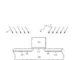
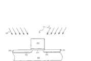
请参阅图1至图3,图1至图3为一现有采用共注入的方法形成超浅结的轻掺杂漏极(LDD)的P型MOS晶体管。如图1所示,该方法提供一基底100,基底100上则设置有一栅极介电层(gate dielectric layer)102与一栅极104。随后对基底100进行一PAI工艺110,以锑(Sb)或锗(Ge)作为主要选择,施以适当的能量与剂量使基底100的硅晶格结构产生破坏,以形成一非晶化区域112。此非晶化的结构用以降低硼的穿隧效应(channeling)与TED效应。Please refer to FIG. 1 to FIG. 3 . FIG. 1 to FIG. 3 are a conventional lightly doped drain (LDD) P-type MOS transistor formed by co-implantation method. As shown in FIG. 1 , the method provides a
请参阅图2。接下来对基底100施行一共注入工艺120,将碳或氟以垂直基底100的角度注入基底100,随后再施以P型掺杂质注入工艺130,最后再进行一第一快速退火(RTA)工艺140,完成P型晶体管的超浅结的轻掺杂漏极(LDD)150的制作。请参阅图3,随后于栅极104侧边形成偏位间隙壁(offset spacer)160,并对基底100再施以一P型掺杂离子注入工艺170以及一第二RTA工艺180,以于偏位间隙壁160两侧的基底100内形成源极/漏极190。See Figure 2. Next, a
然而,由于共注入工艺120以垂直基底100的角度注入基底100,其在后续第一与第二RTA工艺140、180中对于P型掺杂质横向扩散(lateraldiffusion)的控制仍未臻理想。因此,目前该技术领域仍需要一种可有效抑制前述TED效应以及横向扩散的方法,以避免超浅结轻掺杂漏极的掺杂轮廓因扩散而产生改变。However, since the
发明内容Contents of the invention
因此,本发明于此提供一种制作MOS晶体管的方法,尤指一种可有效改善TED效应及短沟道效应的制作MOS晶体管的方法。Therefore, the present invention hereby provides a method for manufacturing a MOS transistor, especially a method for manufacturing a MOS transistor that can effectively improve the TED effect and the short channel effect.
根据本发明,提供一种制作MOS晶体管的方法,该方法首先提供一基底,且该基底上包括有一栅极结构。随后进行一预非晶化(PAI)工艺,以于该栅极结构两侧的该基底内形成一非晶化区域;并进行一共注入(co-implantation)工艺,以于该非晶化区域内注入一共注入掺杂质。接下来进行一第一离子注入工艺与一第一快速退火(RTA)工艺,以于该非晶化区域内注入一第一掺杂质并活化该共注入掺杂质与该第一掺杂质,使该非晶化区域再结晶,而于该栅极结构两侧的该基底内分别形成一轻掺杂漏极(LDD)。之后于该栅极结构的侧壁形成一间隙壁,以及于该间隙壁两侧的该基底内形成一源极/漏极。According to the present invention, a method for manufacturing a MOS transistor is provided. The method firstly provides a substrate, and the substrate includes a gate structure. Then perform a pre-amorphization (PAI) process to form an amorphized region in the substrate on both sides of the gate structure; and perform a co-implantation process to form an amorphized region in the amorphized region The implantation totally implants dopants. Next, a first ion implantation process and a first rapid annealing (RTA) process are performed to implant a first dopant in the amorphized region and activate the co-implantation dopant and the first dopant , recrystallize the amorphized region, and respectively form a lightly doped drain (LDD) in the substrate on both sides of the gate structure. Then a spacer is formed on the sidewall of the gate structure, and a source/drain is formed in the substrate on both sides of the spacer.
根据本发明,另提供一种制作MOS晶体管的方法,该方法首先提供一基底,该基底包括有一栅极结构。之后进行一共注入工艺,以于该栅极结构两侧的该基底内注入一共注入掺杂质,并形成一共注入掺杂区。接下来进行一预非晶化工艺,以于该栅极结构两侧的该基底内形成一非晶化区域,以及进行一第一离子注入工艺,以于该非晶化区域内注入一第一掺杂质。随后进行一第一快速退火工艺,以活化该共注入掺杂质与该第一掺杂质,并使该非晶化区域再结晶,而形成一轻掺杂漏极,以及于该基底内形成一源极/漏极。According to the present invention, there is also provided a method for fabricating a MOS transistor. The method firstly provides a substrate, and the substrate includes a gate structure. Afterwards, a co-implantation process is performed to implant a co-implantation dopant into the substrate on both sides of the gate structure to form a co-implantation doping region. Next, a pre-amorphization process is performed to form an amorphized region in the substrate on both sides of the gate structure, and a first ion implantation process is performed to implant a first ion implantation into the amorphized region. dopant. A first rapid annealing process is then performed to activate the co-implanted dopant and the first dopant, and recrystallize the amorphized region to form a lightly doped drain, and to form a lightly doped drain in the substrate. a source/drain.
根据本发明,更提供一种制作MOS晶体管的方法,该方法首先提供一基底,该基底包括有一栅极结构。随后进行一预非晶化工艺,以于该栅极结构两侧的该基底内形成一非晶化区域;以及进行一第一离子注入工艺,以于该非晶化区域内注入一第一掺杂质。接下来进行一共注入工艺,以于该非晶化区域内再注入一共注入掺杂质。随即进行一第一快速退火工艺,以活化该共注入掺杂质与该第一掺杂质,并使该非晶化区域再结晶,而于该栅极结构两侧的该基底内分别形成一轻掺杂漏极,最后于该基底内形成一源极/漏极。According to the present invention, a method for manufacturing a MOS transistor is further provided. The method firstly provides a substrate, and the substrate includes a gate structure. Then perform a pre-amorphization process to form an amorphized region in the substrate on both sides of the gate structure; and perform a first ion implantation process to implant a first doped ion into the amorphized region. Impurities. Next, a co-implantation process is performed to re-implant a co-implanted dopant into the amorphized region. Immediately, a first rapid annealing process is performed to activate the co-implanted dopant and the first dopant, and recrystallize the amorphized region, and respectively form a The drain is lightly doped, and finally a source/drain is formed in the substrate.
由于本发明所提供的制作MOS晶体管的方法分别于进行预非晶化工艺之前、进行第一离子注入工艺之前以及进行第一离子注入工艺之后进行一共注入工艺,因此于第一快速退火工艺之后,即可减少第一掺杂质横向扩散与TED效应。换句话说,本发明所提供的方法藉由共注入工艺有效控制第一掺杂质的扩散,以获得良好的结轮廓,改善短沟道效应。Since the method for manufacturing MOS transistors provided by the present invention performs a co-implantation process before performing the pre-amorphization process, before performing the first ion implantation process, and after performing the first ion implantation process, after the first rapid annealing process, The lateral diffusion of the first dopant and the TED effect can be reduced. In other words, the method provided by the present invention effectively controls the diffusion of the first dopant through the co-implantation process, so as to obtain a good junction profile and improve the short channel effect.
附图说明Description of drawings
图1至图3为现有采用离子共注入的方法形成超浅结的源极/漏极延伸区域的P型MOS晶体管的示意图;1 to 3 are schematic diagrams of conventional P-type MOS transistors that use ion co-implantation methods to form ultra-shallow junction source/drain extension regions;
图4至图8为本发明所提供的制作MOS晶体管的方法的第一优选实施例示意图;4 to 8 are schematic diagrams of a first preferred embodiment of the method for manufacturing a MOS transistor provided by the present invention;
图9是栅极长度与启始电压下降(roll-off)图;Fig. 9 is a graph of gate length and initial voltage drop (roll-off);
图10至图12为本发明所提供的制作MOS晶体管的方法的第二优选实施例示意图;10 to 12 are schematic diagrams of a second preferred embodiment of the method for manufacturing a MOS transistor provided by the present invention;
图13至图16为本发明所提供的制作MOS晶体管的方法的第三优选实施例示意图。13 to 16 are schematic diagrams of a third preferred embodiment of the method for manufacturing a MOS transistor provided by the present invention.
主要元件符号说明Description of main component symbols
100 基底 102 栅极介电层100
104 栅极 110 预非晶化工艺104 Gate Gate 110 Pre-Amorphization Process
112 非晶化区域 120 共注入工艺112
130 P型掺杂质注入工艺 140 第一快速退火工艺130 P-type
150 轻掺杂漏极(LDD) 160 偏位间隙壁150 Lightly Doped Drain (LDD) 160 Offset Spacer
170 离子注入工艺 180 第二退火工艺170
190 源极/漏极190 source/drain
200 基底 210 栅极结构200
212 栅极介电层 214 栅极212 Gate Dielectric Layer 214 Gate
220 预非晶化工艺 222 非晶化区域220
230 共注入工艺 232 共注入掺杂质230
240 第一离子注入工艺 242 第一掺杂质240 The first
250 第一快速退火工艺 260 轻掺杂漏极(LDD)250 First
270 间隙壁 280 源极/漏极270
300 基底 310 栅极结构300
312 栅极介电层 314 栅极312
320 共注入工艺 322 共注入掺杂质320
330 预非晶化工艺 332 非晶化区域330
340 第一离子注入工艺 342 第一掺杂质340 The first
400 基底 410 栅极结构400
412 栅极介电层 414 栅极412
420 预非晶化工艺 422 非晶化区域420
430 第一离子注入工艺 432 第一掺杂质430 The first
440 共注入工艺 442 共注入掺杂质440
450 第一快速退火工艺 460 轻掺杂漏极(LDD)450 The first rapid annealing process 460 Lightly doped drain (LDD)
具体实施方式Detailed ways
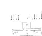
请参阅图4至图8,图4至图8为本发明所提供的制作MOS晶体管的方法的第一优选实施例示意图。如图4所示,首先提供一基底200,基底200可为半导体晶片、硅覆绝缘晶片(silicon-on-insulator,SOI wafer)等,基底200已完成浅沟隔离(STI)工艺以及阱(well)的掺杂工艺,而且基底200上已形成有至少由一栅极介电层212与一栅极214构成的栅极结构210。随后进行一预非晶化(PAI)工艺220,PAI工艺220可为一直角或斜角(angled)的PAI工艺,以于该栅极结构210两侧的基底200内形成一非晶化区域222。Please refer to FIG. 4 to FIG. 8 . FIG. 4 to FIG. 8 are schematic diagrams of a first preferred embodiment of the method for manufacturing a MOS transistor provided by the present invention. As shown in FIG. 4 , a
请参阅图5。接下来进行一共注入(co-implantation)工艺230,以于该非晶化区域222内注入一共注入掺杂质232。值得注意的是,该共注入掺杂质232是以一斜角离子注入工艺注入基底200,亦即此共注入工艺230为一斜角离子注入工艺,且该斜角θ的范围为0~45度;而该共注入掺杂质232包括有碳、氟、或氮。而注入能量可依注入位置而定,如3KeV至20KeV;剂量则可为1×10¹⁵至5×10¹⁵个原子/cm3。See Figure 5. Next, a
请参阅图6。随后进行一第一离子注入工艺240,以于非晶化区域222内注入一第一掺杂质242,且第一掺杂质242与共注入掺杂质232注入于基底200的位置大致相同。且当欲制作的MOS晶体管为P型晶体管时,第一掺杂质242包括有可以提供额外空穴的受主(acceptor),例如硼(B)、镓(Ga)等三价元素;当欲制作的MOS晶体管为N型晶体管时,第一掺杂质242则包括有可以提供额外电子的施主(donor),例如磷和砷等五价元素。随后如图7所示,进行一第一快速退火(RTA)工艺250,利用炉管(furnace)或快速升温处理(rapid thermal process,以下简称RTP),于1000~1100℃的温度下活化共注入掺杂质232与第一掺杂质242,并使该非晶化区域222再结晶,而于非晶化区域222内分别形成一轻掺杂漏极(LDD)260。See Figure 6. Then a first
请参阅图8,接下来于栅极结构210的侧壁形成一间隙壁270,间隙壁270可为一氧化物-氮化物-氧化物偏位间隙壁(ONO offset spacer)等。在完成间隙壁270的制作后,再于间隙壁270两侧的基底200中进行一第二离子注入工艺,以于间隙壁270两侧的基底200内形成一源极/漏极预定区域。随后进行一第三RTA工艺,以于源极/漏极预定区域内形成一源极/漏极280,该些步骤为本领域技术人员所熟知,故于此不再赘述。此外,亦可依工艺或产品需求,于完成源极/漏极280的制作后,移除间隙壁270。至此完成本发明所提供的可有效改善TED效应及横向扩散的MOS晶体管制作方法。Referring to FIG. 8 , next, a
请再参阅图5,值得注意的是,于本第一优选实施例中,还可于进行共注入工艺230之后即进行一第二RTA工艺,利用炉管RTP提供一1000~1100℃的高温先行活化该共注入掺杂质232,使得共注入掺杂质232先与空隙缺陷形成键结。因此于后续工艺中,更可降低因空隙缺陷造成的TED效应。Please refer to FIG. 5 again. It is worth noting that in this first preferred embodiment, a second RTA process can be performed after the
另外,于本第一优选实施例中,还可于进行共注入工艺230之前,增加一口袋型离子注入(pocket implantation)工艺,以于非晶化区域222与基底200交界附近形成一口袋型掺杂区。当然,此口袋型离子注入工艺亦可于共注入工艺230之后始进行,以抑制不正常的穿通(punch through)现象的发生。In addition, in the first preferred embodiment, before the
请参阅图9。图9是栅极长度与启始电压下降(roll-off)关系图,其横轴表示多晶硅栅极蚀刻后(after-etch-inspect,AEI)临界尺寸(critical dimension,CD),以微米(μm)为单位,而纵轴表示启始电压Vts,以伏特(Volt)为单位,其中菱形点为现有MOS晶体管的量测值、圆形点代表本第一优选实施例的量测值、而方形点则代表标准值。如图9所示,当现有多晶硅栅极长度越小时,越无法控制短沟道效应,MOS晶体管的启始电压亦随之下降;而当多晶硅栅极长度降到0.03μm时,现有MOS晶体管的启始电压已经下降到0,也就是说,该MOS晶体管根本无法使用。而根据本发明所提供的第一优选实施例所得的MOS晶体管,其启始电压可提高至0.15至0.35,而符合期待的标准值,故可知本发明所提供的制作MOS晶体管的方法的确可有效改善TED效应以及短沟道效应。See Figure 9. Figure 9 is a graph showing the relationship between the gate length and the initial voltage drop (roll-off). ) as the unit, and the vertical axis represents the starting voltage Vts in volts (Volt), wherein the rhombus point is the measured value of the existing MOS transistor, and the circular point represents the measured value of the first preferred embodiment, The square dots represent standard values. As shown in Figure 9, when the length of the existing polysilicon gate is smaller, the short channel effect cannot be controlled, and the starting voltage of the MOS transistor also decreases; and when the length of the polysilicon gate is reduced to 0.03 μm, the existing MOS The starting voltage of the transistor has dropped to 0, that is, the MOS transistor cannot be used at all. And according to the MOS transistor obtained by the first preferred embodiment provided by the present invention, its starting voltage can be increased to 0.15 to 0.35, and meets the expected standard value, so it can be known that the method for making MOS transistor provided by the present invention is indeed effective. Improve TED effect and short channel effect.
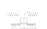
请参阅图10至图12。图10至图12为本发明所提供的制作MOS晶体管的方法的第二优选实施例示意图。如图10所示,首先提供一基底300,基底300上包括至少由一栅极介电层312与一栅极314构成的栅极结构310。随后进行一共注入工艺320,以于此栅极结构310两侧的基底300内注入一共注入掺杂质322。值得注意的是,该共注入掺杂质322是以一斜角离子注入工艺注入基底300,亦即此共注入工艺320为一斜角离子注入工艺,且该斜角θ的范围为0~45度;而该共注入掺杂质包括有碳、氟、或氮。而注入能量可依注入位置而定,如3KeV至20KeV;剂量则可为1×10¹⁵至5×10¹⁵个原子/cm3。See Figures 10 through 12. 10 to 12 are schematic diagrams of a second preferred embodiment of the method for manufacturing a MOS transistor provided by the present invention. As shown in FIG. 10 , firstly, a
请参阅图11与图12。接下来对基底300进行一PAI工艺330,PAI工艺330亦可为一直角或斜角(angled)的PAI工艺,以于栅极结构310两侧的基底300内形成一非晶化区域332。随后如图12所示,进行一第一离子注入工艺340,以于非晶化区域332内注入一第一掺杂质342,且第一掺杂质342与共注入掺杂质322注入于基底300的位置大致相同。Please refer to Figure 11 and Figure 12. Next, a
随后如前所述,进行一第一快速退火(RTA)工艺,利用炉管或RTP,于1000~1100℃的温度下活化共注入掺杂质322与第一掺杂质342,并使此非晶化区域332再结晶,而于栅极结构310两侧的基底300内分别形成一轻掺杂漏极(LDD)。当欲制作的MOS晶体管为P型晶体管时,第一掺杂质342包括有可以提供额外空穴的受主,例如硼等物质;当欲制作的MOS晶体管为N型晶体管时,第一掺杂质342则包括有可以提供额外电子的施主,例如磷和砷等物质。接下来于栅极结构310的侧壁形成一间隙壁,以及于间隙壁两侧的基底300内进行第二离子掺杂工艺与第三RTA工艺,以形成一源极/漏极。而该些间隙壁可依工艺或产品需求,于完成源极/漏极的制作后移除。该些工艺系与第一优选实施例相同,故于此不再赘述。Then, as mentioned above, a first rapid annealing (RTA) process is performed, using a furnace tube or RTP to activate the
于本第二优选实施例中,可于进行共注入工艺320后,立即进行一第二RTA工艺,利用炉管或RTP提供一1000~1100℃的高温先行活化共注入掺杂质322,使得共注入掺杂质322先与空隙缺陷形成键结。因此于后续工艺中,更可降低因空隙缺陷造成的TED效应。In the second preferred embodiment, after performing the
另外,于本第二优选实施例中,亦可于进行共注入工艺320之前,增加一口袋型离子注入工艺,以于非晶化区域332与基底300交界附近形成一口袋型掺杂区。当然,此口袋型离子注入工艺亦可于共注入工艺320之后始进行,以抑制不正常的穿通现象的发生。In addition, in the second preferred embodiment, before the
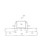
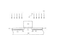
请参阅图13至图16。图13至图16为本发明所提供的制作MOS晶体管的方法的第三优选实施例示意图。如图13所示,首先提供一基底400,基底400上包括至少由一栅极介电层412与一栅极414构成的栅极结构410。随后进行一预非晶化工艺(PAI)工艺420,PAI工艺420亦可为一直角或斜角(angled)的PAI工艺,以于该栅极结构410两侧的该基底400内形成一非晶化区域422。See Figures 13 through 16. 13 to 16 are schematic diagrams of a third preferred embodiment of the method for manufacturing a MOS transistor provided by the present invention. As shown in FIG. 13 , firstly, a
请参阅图14与图15。接下来对栅极结构410两侧的基底400进行一第一离子注入工艺430,以于非晶化区域422内注入一第一掺杂质432。当欲制作的MOS晶体管为P型晶体管时,第一掺杂质432包括有硼等受主;当欲制作的MOS晶体管为N型晶体管时,第一掺杂质432则包括有磷和砷等施主。Please refer to Figure 14 and Figure 15. Next, a first
随后如图15所示,进行一共注入工艺440,以于栅极结构410两侧的基底400内注入一共注入掺杂质442。值得注意的是,共注入掺杂质442是以一斜角离子注入工艺注入基底400,且该斜角θ的范围为0~45度;而该共注入掺杂质包括有碳、氟、或氮。而注入能量可依注入位置而定,如3KeV至20KeV;剂量则可为1×10¹⁵至5×10¹⁵个原子/cm3。Subsequently, as shown in FIG. 15 , a
请参阅图16。进行一第一RTA工艺450,于1000~1100℃的温度下活化第一掺杂质432与共注入掺杂质442,并使非晶化区域422再结晶,而于栅极结构410两侧的基底400内分别形成一轻掺杂漏极(LDD)460。See Figure 16. Perform a first RTA process 450 to activate the
接下来于栅极结构410的侧壁形成一间隙壁,以及于间隙壁两侧的基底400内进行第二离子掺杂工艺与第二RTA工艺,以形成一源极/漏极。而该些间隙壁可依工艺或产品需求,于完成源极/漏极的制作后移除。由于该些工艺与第一优选实施例相同,故于此不再赘述。同样地,于本第三优选实施例中,亦可于进行共注入工艺440之前,增加一口袋型离子注入工艺,以于非晶化区域422之间形成一口袋型掺杂区。当然,此口袋型离子注入工艺亦可于共注入工艺440之后始进行,以抑制不正常的穿通现象的发生。Next, a spacer is formed on the sidewall of the
另外,本发明所提供的制作MOS晶体管的方法,可结合选择性应变结构(selective strain scheme)技术,如用以制作具有高张应力薄膜的NMOS晶体管或具有高压应力薄膜的PMOS晶体管,改善元件效能,更提升MOS晶体管元件的载流子迁移率与驱动电流。亦可结合嵌入式硅锗源极/漏极(recessed SiGe Source/darin)或嵌入式硅碳源极/漏极(recessed SiCSource/drain)结构,改善寄生电阻问题,增加驱动电流与速度。In addition, the method for making MOS transistors provided by the present invention can be combined with selective strain scheme technology, such as for making NMOS transistors with high tensile stress films or PMOS transistors with high voltage stress films, to improve device performance , and further enhance the carrier mobility and driving current of the MOS transistor element. It can also be combined with embedded silicon germanium source/drain (recessed SiGe Source/darin) or embedded silicon carbon source/drain (recessed SiCSource/drain) structure to improve the problem of parasitic resistance and increase the driving current and speed.
由于本发明所提供的制作MOS晶体管的方法是分别于进行PAI工艺之前、进行第一离子注入工艺之前以及进行第一离子注入工艺之后进行一共注入工艺,因此于RTA工艺之后,即可该些共掺杂质可与空隙缺陷形成键结,而避免第一掺杂质因空隙缺陷所造成的TED效应与横向扩散的发生。换句话说,本发明所提供的方法是藉由共注入工艺有效控制第一掺杂质的扩散,以获得良好的结轮廓,改善短沟道效应。Since the method for manufacturing MOS transistors provided by the present invention performs a co-implantation process before the PAI process, before the first ion implantation process, and after the first ion implantation process, after the RTA process, these co-implantation processes can be performed. The dopant can form a bond with the void defect, so as to avoid the TED effect and lateral diffusion of the first dopant caused by the void defect. In other words, the method provided by the present invention is to effectively control the diffusion of the first dopant through the co-implantation process, so as to obtain a good junction profile and improve the short channel effect.
以上所述仅为本发明的优选实施例,凡依本发明权利要求所做的均等变化与修饰,皆应属本发明的涵盖范围。The above descriptions are only preferred embodiments of the present invention, and all equivalent changes and modifications made according to the claims of the present invention shall fall within the scope of the present invention.
Claims (45)
Priority Applications (1)
| Application Number | Priority Date | Filing Date | Title |
|---|---|---|---|
| CNB2006101433975ACN100527370C (en) | 2006-11-08 | 2006-11-08 | method for manufacturing metal oxide semiconductor transistor |
Applications Claiming Priority (1)
| Application Number | Priority Date | Filing Date | Title |
|---|---|---|---|
| CNB2006101433975ACN100527370C (en) | 2006-11-08 | 2006-11-08 | method for manufacturing metal oxide semiconductor transistor |
Publications (2)
| Publication Number | Publication Date |
|---|---|
| CN101179027A CN101179027A (en) | 2008-05-14 |
| CN100527370Ctrue CN100527370C (en) | 2009-08-12 |
Family
ID=39405212
Family Applications (1)
| Application Number | Title | Priority Date | Filing Date |
|---|---|---|---|
| CNB2006101433975AActiveCN100527370C (en) | 2006-11-08 | 2006-11-08 | method for manufacturing metal oxide semiconductor transistor |
Country Status (1)
| Country | Link |
|---|---|
| CN (1) | CN100527370C (en) |
Families Citing this family (10)
| Publication number | Priority date | Publication date | Assignee | Title |
|---|---|---|---|---|
| US20110039390A1 (en)* | 2009-08-14 | 2011-02-17 | Taiwan Semiconductor Manufacturing Company, Ltd. | Reducing Local Mismatch of Devices Using Cryo-Implantation |
| CN102403227B (en)* | 2010-09-17 | 2013-10-23 | 中芯国际集成电路制造(北京)有限公司 | Manufacturing method for stepped silicon germanium source/drain structures |
| CN102468167B (en)* | 2010-11-01 | 2013-11-06 | 中芯国际集成电路制造(上海)有限公司 | Mos transistor and manufacturing method thereof |
| CN102487009B (en)* | 2010-12-02 | 2014-06-04 | 中芯国际集成电路制造(上海)有限公司 | Manufacturing method of source electrode and drain electrode of N metal-oxide semiconductor field effect transistor (MOS) device |
| KR101868803B1 (en)* | 2011-11-04 | 2018-06-22 | 삼성전자주식회사 | Method of manufacturing a semiconductor device using stress memorization technique(SMT) |
| CN102623346A (en)* | 2012-03-27 | 2012-08-01 | 上海宏力半导体制造有限公司 | Transistor manufacturing method |
| CN103681248B (en)* | 2012-09-04 | 2017-02-01 | 中芯国际集成电路制造(上海)有限公司 | Production method for semiconductor device |
| CN103779281A (en)* | 2012-10-19 | 2014-05-07 | 德州仪器公司 | How to Make a Transistor |
| CN103972102A (en)* | 2014-04-22 | 2014-08-06 | 上海华力微电子有限公司 | Ultra-shallow junction forming method and semiconductor device forming method |
| CN114121659B (en)* | 2020-08-28 | 2023-10-03 | 长鑫存储技术有限公司 | Preparation method of semiconductor device |
Citations (3)
| Publication number | Priority date | Publication date | Assignee | Title |
|---|---|---|---|---|
| US6682980B2 (en)* | 2002-05-06 | 2004-01-27 | Texas Instruments Incorporated | Fabrication of abrupt ultra-shallow junctions using angled PAI and fluorine implant |
| US20050158956A1 (en)* | 2004-01-16 | 2005-07-21 | Chartered Semiconductor Manufacturing Ltd. | Dual step source/drain extension junction anneal to reduce the junction depth: multiple-pulse low energy laser anneal coupled with rapid thermal anneal |
| US20060160338A1 (en)* | 2004-12-17 | 2006-07-20 | Applied Materials, Inc. | Method of ion implantation to reduce transient enhanced diffusion |
- 2006
- 2006-11-08CNCNB2006101433975Apatent/CN100527370C/enactiveActive
Patent Citations (3)
| Publication number | Priority date | Publication date | Assignee | Title |
|---|---|---|---|---|
| US6682980B2 (en)* | 2002-05-06 | 2004-01-27 | Texas Instruments Incorporated | Fabrication of abrupt ultra-shallow junctions using angled PAI and fluorine implant |
| US20050158956A1 (en)* | 2004-01-16 | 2005-07-21 | Chartered Semiconductor Manufacturing Ltd. | Dual step source/drain extension junction anneal to reduce the junction depth: multiple-pulse low energy laser anneal coupled with rapid thermal anneal |
| US20060160338A1 (en)* | 2004-12-17 | 2006-07-20 | Applied Materials, Inc. | Method of ion implantation to reduce transient enhanced diffusion |
Also Published As
| Publication number | Publication date |
|---|---|
| CN101179027A (en) | 2008-05-14 |
Similar Documents
| Publication | Publication Date | Title |
|---|---|---|
| CN100527370C (en) | method for manufacturing metal oxide semiconductor transistor | |
| US7700450B2 (en) | Method for forming MOS transistor | |
| US7396717B2 (en) | Method of forming a MOS transistor | |
| US9041126B2 (en) | Deeply depleted MOS transistors having a screening layer and methods thereof | |
| US9246006B2 (en) | Recrystallization of source and drain blocks from above | |
| US20060284249A1 (en) | Impurity co-implantation to improve transistor performance | |
| US7795101B2 (en) | Method of forming a MOS transistor | |
| US20080121992A1 (en) | Semiconductor device including diffusion barrier region and method of fabricating the same | |
| US20060275964A1 (en) | Semiconductor device and method for fabricating the same | |
| CN102074476B (en) | Forming method of N-channel metal oxide semiconductor (NMOS) transistor | |
| CN104051237B (en) | Low thermal budget schemes in semiconductor device fabrication | |
| US8951877B2 (en) | Transistor with embedded strain-inducing material formed in cavities based on an amorphization process and a heat treatment | |
| US20110097868A1 (en) | Method for fabricating p-channel field-effect transistor (fet) | |
| US7151032B2 (en) | Methods of fabricating semiconductor devices | |
| CN101930922B (en) | Production method of MOS (Metal Oxide Semiconductor) transistor | |
| US8536034B2 (en) | Methods of forming stressed silicon-carbon areas in an NMOS transistor | |
| CN111129141A (en) | Preparation method of semiconductor device and semiconductor device obtained by preparation method | |
| CN101814456B (en) | Integrated circuit device and method of forming the same | |
| CN104078427B (en) | SRAM (Static Random Access Memory) and preparation method thereof | |
| US8664073B2 (en) | Method for fabricating field-effect transistor | |
| CN108878526A (en) | Semiconductor structure and forming method thereof | |
| JP2005347731A (en) | Semiconductor device and manufacturing method thereof | |
| TW200820348A (en) | Method for forming MOS transistor | |
| CN103227114A (en) | Method for forming ultra-shallow junction plane | |
| KR20090071945A (en) | Manufacturing method of semiconductor device |
Legal Events
| Date | Code | Title | Description |
|---|---|---|---|
| C06 | Publication | ||
| PB01 | Publication | ||
| C10 | Entry into substantive examination | ||
| SE01 | Entry into force of request for substantive examination | ||
| C14 | Grant of patent or utility model | ||
| GR01 | Patent grant |