CN100524848C - Light emitting diodes including light extraction modifications and methods of making the same - Google Patents
Light emitting diodes including light extraction modifications and methods of making the sameDownload PDFInfo
- Publication number
- CN100524848C CN100524848CCNB028044177ACN02804417ACN100524848CCN 100524848 CCN100524848 CCN 100524848CCN B028044177 ACNB028044177 ACN B028044177ACN 02804417 ACN02804417 ACN 02804417ACN 100524848 CCN100524848 CCN 100524848C
- Authority
- CN
- China
- Prior art keywords
- substrate
- diode
- diode region
- light emitting
- light
- Prior art date
- Legal status (The legal status is an assumption and is not a legal conclusion. Google has not performed a legal analysis and makes no representation as to the accuracy of the status listed.)
- Expired - Lifetime
Links
Images


Classifications
- H—ELECTRICITY
- H10—SEMICONDUCTOR DEVICES; ELECTRIC SOLID-STATE DEVICES NOT OTHERWISE PROVIDED FOR
- H10H—INORGANIC LIGHT-EMITTING SEMICONDUCTOR DEVICES HAVING POTENTIAL BARRIERS
- H10H20/00—Individual inorganic light-emitting semiconductor devices having potential barriers, e.g. light-emitting diodes [LED]
- H10H20/80—Constructional details
- H10H20/81—Bodies
- H10H20/819—Bodies characterised by their shape, e.g. curved or truncated substrates
- H—ELECTRICITY
- H10—SEMICONDUCTOR DEVICES; ELECTRIC SOLID-STATE DEVICES NOT OTHERWISE PROVIDED FOR
- H10H—INORGANIC LIGHT-EMITTING SEMICONDUCTOR DEVICES HAVING POTENTIAL BARRIERS
- H10H20/00—Individual inorganic light-emitting semiconductor devices having potential barriers, e.g. light-emitting diodes [LED]
- H10H20/80—Constructional details
- H10H20/83—Electrodes
- H10H20/832—Electrodes characterised by their material
- H10H20/835—Reflective materials
- H—ELECTRICITY
- H01—ELECTRIC ELEMENTS
- H01L—SEMICONDUCTOR DEVICES NOT COVERED BY CLASS H10
- H01L2224/00—Indexing scheme for arrangements for connecting or disconnecting semiconductor or solid-state bodies and methods related thereto as covered by H01L24/00
- H01L2224/01—Means for bonding being attached to, or being formed on, the surface to be connected, e.g. chip-to-package, die-attach, "first-level" interconnects; Manufacturing methods related thereto
- H01L2224/26—Layer connectors, e.g. plate connectors, solder or adhesive layers; Manufacturing methods related thereto
- H01L2224/31—Structure, shape, material or disposition of the layer connectors after the connecting process
- H01L2224/32—Structure, shape, material or disposition of the layer connectors after the connecting process of an individual layer connector
- H01L2224/3201—Structure
- H01L2224/32012—Structure relative to the bonding area, e.g. bond pad
- H01L2224/32014—Structure relative to the bonding area, e.g. bond pad the layer connector being smaller than the bonding area, e.g. bond pad
- H—ELECTRICITY
- H01—ELECTRIC ELEMENTS
- H01L—SEMICONDUCTOR DEVICES NOT COVERED BY CLASS H10
- H01L2224/00—Indexing scheme for arrangements for connecting or disconnecting semiconductor or solid-state bodies and methods related thereto as covered by H01L24/00
- H01L2224/01—Means for bonding being attached to, or being formed on, the surface to be connected, e.g. chip-to-package, die-attach, "first-level" interconnects; Manufacturing methods related thereto
- H01L2224/42—Wire connectors; Manufacturing methods related thereto
- H01L2224/47—Structure, shape, material or disposition of the wire connectors after the connecting process
- H01L2224/48—Structure, shape, material or disposition of the wire connectors after the connecting process of an individual wire connector
- H01L2224/4805—Shape
- H01L2224/4809—Loop shape
- H01L2224/48091—Arched
- H—ELECTRICITY
- H01—ELECTRIC ELEMENTS
- H01L—SEMICONDUCTOR DEVICES NOT COVERED BY CLASS H10
- H01L2224/00—Indexing scheme for arrangements for connecting or disconnecting semiconductor or solid-state bodies and methods related thereto as covered by H01L24/00
- H01L2224/73—Means for bonding being of different types provided for in two or more of groups H01L2224/10, H01L2224/18, H01L2224/26, H01L2224/34, H01L2224/42, H01L2224/50, H01L2224/63, H01L2224/71
- H01L2224/732—Location after the connecting process
- H01L2224/73251—Location after the connecting process on different surfaces
- H01L2224/73265—Layer and wire connectors
- H—ELECTRICITY
- H01—ELECTRIC ELEMENTS
- H01L—SEMICONDUCTOR DEVICES NOT COVERED BY CLASS H10
- H01L2924/00—Indexing scheme for arrangements or methods for connecting or disconnecting semiconductor or solid-state bodies as covered by H01L24/00
- H01L2924/01—Chemical elements
- H01L2924/01079—Gold [Au]
- H—ELECTRICITY
- H01—ELECTRIC ELEMENTS
- H01L—SEMICONDUCTOR DEVICES NOT COVERED BY CLASS H10
- H01L2924/00—Indexing scheme for arrangements or methods for connecting or disconnecting semiconductor or solid-state bodies as covered by H01L24/00
- H01L2924/013—Alloys
- H01L2924/0132—Binary Alloys
- H01L2924/01322—Eutectic Alloys, i.e. obtained by a liquid transforming into two solid phases
- H—ELECTRICITY
- H01—ELECTRIC ELEMENTS
- H01L—SEMICONDUCTOR DEVICES NOT COVERED BY CLASS H10
- H01L2924/00—Indexing scheme for arrangements or methods for connecting or disconnecting semiconductor or solid-state bodies as covered by H01L24/00
- H01L2924/10—Details of semiconductor or other solid state devices to be connected
- H01L2924/102—Material of the semiconductor or solid state bodies
- H01L2924/1025—Semiconducting materials
- H01L2924/10251—Elemental semiconductors, i.e. Group IV
- H01L2924/10253—Silicon [Si]
- H—ELECTRICITY
- H01—ELECTRIC ELEMENTS
- H01L—SEMICONDUCTOR DEVICES NOT COVERED BY CLASS H10
- H01L2924/00—Indexing scheme for arrangements or methods for connecting or disconnecting semiconductor or solid-state bodies as covered by H01L24/00
- H01L2924/10—Details of semiconductor or other solid state devices to be connected
- H01L2924/11—Device type
- H01L2924/12—Passive devices, e.g. 2 terminal devices
- H01L2924/1203—Rectifying Diode
- H01L2924/12032—Schottky diode
- H—ELECTRICITY
- H01—ELECTRIC ELEMENTS
- H01L—SEMICONDUCTOR DEVICES NOT COVERED BY CLASS H10
- H01L2924/00—Indexing scheme for arrangements or methods for connecting or disconnecting semiconductor or solid-state bodies as covered by H01L24/00
- H01L2924/10—Details of semiconductor or other solid state devices to be connected
- H01L2924/11—Device type
- H01L2924/12—Passive devices, e.g. 2 terminal devices
- H01L2924/1204—Optical Diode
- H01L2924/12041—LED
- H—ELECTRICITY
- H10—SEMICONDUCTOR DEVICES; ELECTRIC SOLID-STATE DEVICES NOT OTHERWISE PROVIDED FOR
- H10H—INORGANIC LIGHT-EMITTING SEMICONDUCTOR DEVICES HAVING POTENTIAL BARRIERS
- H10H20/00—Individual inorganic light-emitting semiconductor devices having potential barriers, e.g. light-emitting diodes [LED]
- H10H20/80—Constructional details
- H10H20/81—Bodies
- H10H20/814—Bodies having reflecting means, e.g. semiconductor Bragg reflectors
- H—ELECTRICITY
- H10—SEMICONDUCTOR DEVICES; ELECTRIC SOLID-STATE DEVICES NOT OTHERWISE PROVIDED FOR
- H10H—INORGANIC LIGHT-EMITTING SEMICONDUCTOR DEVICES HAVING POTENTIAL BARRIERS
- H10H20/00—Individual inorganic light-emitting semiconductor devices having potential barriers, e.g. light-emitting diodes [LED]
- H10H20/80—Constructional details
- H10H20/81—Bodies
- H10H20/819—Bodies characterised by their shape, e.g. curved or truncated substrates
- H10H20/82—Roughened surfaces, e.g. at the interface between epitaxial layers
- H—ELECTRICITY
- H10—SEMICONDUCTOR DEVICES; ELECTRIC SOLID-STATE DEVICES NOT OTHERWISE PROVIDED FOR
- H10H—INORGANIC LIGHT-EMITTING SEMICONDUCTOR DEVICES HAVING POTENTIAL BARRIERS
- H10H20/00—Individual inorganic light-emitting semiconductor devices having potential barriers, e.g. light-emitting diodes [LED]
- H10H20/80—Constructional details
- H10H20/85—Packages
- H10H20/855—Optical field-shaping means, e.g. lenses
- H10H20/856—Reflecting means
- H—ELECTRICITY
- H10—SEMICONDUCTOR DEVICES; ELECTRIC SOLID-STATE DEVICES NOT OTHERWISE PROVIDED FOR
- H10H—INORGANIC LIGHT-EMITTING SEMICONDUCTOR DEVICES HAVING POTENTIAL BARRIERS
- H10H20/00—Individual inorganic light-emitting semiconductor devices having potential barriers, e.g. light-emitting diodes [LED]
- H10H20/80—Constructional details
- H10H20/85—Packages
- H10H20/857—Interconnections, e.g. lead-frames, bond wires or solder balls
Landscapes
- Led Devices (AREA)
- Led Device Packages (AREA)
Abstract
Description
The cross reference of some provisional application patents
The application's request proposed in February 1 calendar year 2001, sequence number is 60/265,707, title is the provisional application of " Light Emitting Diode With Optically TransparentSilicon Carbide Substrate (light-emitting diode that the optical clear silicon carbide substrates is arranged) ", with propose in July 23 calendar year 2001, sequence number is 60/307,235, title is the interests of the provisional application of " Light Emitting Diodes Including Modifications forLight Extraction and Manufacturing Methods Therefor (Light-emitting Diode And Its Making Method that comprises light extraction remodeling) ", their both contents are in this complete as a reference introducing, as statement fully herein.
Technical field
The present invention relates to microelectronic component and its manufacture method, more specifically, relate to light-emitting diode (LED) and preparation method thereof.
Background technology
Light-emitting diode is widely used in consumption and commercial the application.As well-known to persons skilled in the art that light-emitting diode is usually included in the diode region on the microelectronic substrate.Microelectronic substrate comprises, for example, and GaAs, gallium phosphide and their alloy, carborundum and/or sapphire.The continuous development of LED has produced the light source of efficient and mechanically robust, and this light source can cover and exceed the spectrum of visible-range.These characteristics can make multiple new display application become possibility in conjunction with the potential long service live of solid state device, also can make LED be in the position of competing mutually with the incandescent lamp and the fluorescent lamp of fine establishment.
A cost that measurement standard is every lumen of LED efficient.To LED, the cost of every lumen can be the function of the ability of cost of manufacture, LED material internal quantum efficiency and the coupling of each led chip or the light that extraction device produces.Comment about the light extraction problem, can be the textbook of " HighBrightness Light Emitting Diodes (high brightness LED) " referring to people's such as Academic Press (Science Press) Stringfellow in 1997 title, particularly the title of Craford is the chapter 2 of " Overview of Device Issues in High-Brightness Light Emitting Diodes (the device problem comment of high brightness LED) ", the 47-63 page or leaf.
Light extraction is realized by for example relevant with the material of making diode region and substrate a lot of methods.For example, in GaAs and gallium phosphide material system, thick p type top side Window layer can be used for light extraction.Because in GaAs/gallium phosphide material system, adopt liquid phase and/or vapor phase epitaxy method, high epitaxial growth speed is possible, therefore can the growing p-type Window layer.In addition, because the conductivity of p type top side Window layer also can obtain current spread.There are high corrosion rate and height to corrode optionally chemical corrosion and also can be used to be removed to the small part substrate, if this substrate is an optical absorption.Distributed Bragg reflector (distributed Braggreflector) is also grown absorbing between substrate and the diode region, with to emitter region and uptake zone uncoupling.
Other light extraction method can comprise to be made diode region and/or substrate mechanical molding or forms texture.Yet, still be desirable to provide further other light extraction technology of improving extraction efficiency.In addition, also wish to increase the area of led chip, from about 0.1mm2To bigger area, thereby provide bigger LED.Unfortunately, to higher power/intensity and/or other application, when chip size scaled up, the validity of these forming techniques no longer kept.
Recently a lot of development interest and business activity focused in carborundum or on the LED that makes because these LED can partly launch light at the indigo plant/green glow of visible spectrum.For example see, people such as Edmond, title is the United States Patent (USP) 5 of " Blue Light-Emitting Diode With HighExternal Quantum Efficiency (blue light emitting diode of high external quantum efficiency) ", 416,342, transferred the application's assignee, its content is in this complete as a reference introducing, as statement fully herein.Also interesting to comprising the LED on the silicon carbide substrates based on the diode of gallium nitride, because these devices also can high efficiency light-emitting.For example see, authorize people such as Linthicum, title is the United States Patent (USP) 6 of " Pendeoepitaxial GalliumNitride Semiconductor Layers On Silicon Carbide Substrates ", 177,688, its content is in this complete as a reference introducing, as statement fully herein.
In such carborundum LED or the gallium nitride based LED on the carborundum, be difficult to adopt common light extraction technology.For example, because low relatively gallium nitride growth rate, so be difficult to use thick p type Window layer.Equally, LED although it is so can be benefited from use Bragg reflector and/or substrate removal technology, but is difficult to make reflector between substrate and gallium nitride diode district, and/or is difficult to corrosion and removes partially carbonized at least silicon substrate.
Edmond, title is the United States Patent (USP) 4 of " Method of Production of light EmittingDiodes (production method of light-emitting diode) ", 966,862, transferred the application's assignee, its content is in this complete as a reference introducing, as statement fully herein, a kind of method has been described, on the single substrate of semi-conducting material, make a plurality of light-emitting diodes.This method is used for multiple structure, and wherein substrate comprises the epitaxial loayer of semi-conducting material of the same race, and this epitaxial loayer comprises the p type and the n section bar bed of material in regular turn, determines a p-n junction therebetween.With predetermined pattern corrosion epitaxial loayer and substrate, with the precursor of definite single diode, corrosion is enough dark so that form the table top of delineating the p-n junction in each diode precursor mutually in epitaxial loayer.From the edge of epitaxial loayer with between table top, substrate,, is kept enough substrates simultaneously and is used to keep its mechanical stability so that determine the side part of the diode precursor in the substrate to desired depth by cutting below groove.Ohmic contact is added on epitaxial loayer and the substrate, and an insulation material layer is formed on the diode precursor.Insulating barrier covers any part on a surface of those epitaxial loayer that is not covered by ohmic contact parts, the substrate adjacent with table top and the lateral parts of substrate.As a result, the knot of the substrate of each diode part and lateral parts except that by the ohmic contact with electrically contact insulation.When diode was isolated mutually, they can be installed in the conductive epoxy resin downwards with the knot edge usually, and are indifferent to epoxy resin with the resulting diode of short circuit.See United States Patent (USP) 4,966,862 summary.
Carter, Jr., title is the United States Patent (USP) 5 of " High Efficiency Light EmittingDiodes From Bipolar Gallium Nitride (bipolar gallium nitride efficient LED) ", 210,051, transferred the application's assignee, its content is in this complete as a reference introducing, as statement fully herein, described growing method a kind of intrinsic, unadulterated substantially mono-crystal gallium nitride, donor concentration is 7 * 1017Cm3Or it is littler.This method comprises nitrogenous source is incorporated in the reative cell that contains growing surface, simultaneously the gallium source is incorporated into same reative cell, guides nitrogen-atoms and gallium atom simultaneously to the growing surface with growing gallium nitride.This method also comprises, keep simultaneously growing surface sufficiently high temperature with offer the bump growing surface gallium atom and the enough surface mobilities of nitrogen-atoms, to arrive and to move to suitable lattice position, thereby set up good crystallinity, set up effective attachment coefficient, thereby the epitaxial loayer of growing gallium nitride on growing surface, but the dividing potential drop of nitrogen element is enough low again in the reative cell, make under other environmental condition of reative cell, reach and the heat balance air pressure of those nitrogen elements gallium nitride, thereby make the nitrogen loss minimum in the gallium nitride, make in the epitaxial loayer of formation the nitrogen room minimum.See United States Patent (USP) 5,210,051 summary.
According to the above discussion, expectation has improved light extraction technology to LED, particularly the LED that is made by carborundum, the LED that is made by the gallium nitride of carborundum and/or large-area relatively LED is arranged.
Summary of the invention
Light-emitting diode according to some embodiments of the present invention comprises, the substrate that first and second opposite faces are arranged, this substrate is transparent to the light radiation of predetermined wavelength range, and substrate is patterned to determine stretching into a plurality of bearings (pedestal) of substrate from first towards second face in cross section.Herein the term of Cai Yonging " transparent ", be finger element, for example substrate, floor or district allow some or all optical radiations in the predetermined wavelength range by it, that is to say, be not opaque.When applying voltage on diode region, the light that the diode region on second is configured to launch predetermined wavelength range enters substrate.In other embodiments, on diode region, the mounting bracket relative with substrate be configured to support diode region, when on diode region, applying voltage, make the light that enters substrate from the diode region emission just send from first face.In certain embodiments, the light-emitting diode upside-down mounting on backed transparent substrates has the diode region adjacent with mounting bracket on mounting bracket, and the substrate relative with mounting bracket is used for the light emission by substrate.In other embodiments, the light-emitting diode on backed transparent substrates is installed on the mounting bracket, and substrate and mounting bracket are adjacent, and diode region is relative with mounting bracket.Like this, also can provide a kind of non-flip-chip to install.
In other embodiments of the invention, reflector also is provided between mounting bracket and diode region or the substrate.Reflector also can be set like this: when applying voltage on diode region, the light from the diode region emission is reflected back, and by diode region, by substrate, send from bearing.In other embodiments, between diode region and reflector, also can provide transparency electrode.In other other embodiment, solder preform spare and/or other weld zone can be provided between reflector and mounting bracket, and/or adjacent relative with first with diode region, can provide optical element, for example window or lens.In other other embodiment, diode region comprises periphery and the middle body that at least one is surrounded by periphery, light-emitting diode also is included at least one electrode on the diode region, and it is to be limited within least one middle body, does not reach on the periphery.Be appreciated that middle body not necessarily will be in the central authorities of diode region.
In other embodiments of the invention, the substrate of LED and/or the contact structures of diode region comprise the transparent ohmic district, reflector, Resistance and weld zone.The transparent ohmic district provides and electrically contacts and/or current expansion.Reflector reflects some incident radiations at least, and also can provide current expansion.Resistance protection reflector and/or ohmic region.The weld zone arrives mounting bracket to the LED welded encapsulation.In certain embodiments, the function of transparent ohmic district and reflector can be merged into single ohm and reflector area.According to embodiments of the invention, contact structures also can be used with the carborundum LED of routine, gallium nitride based LED and/or other LED on the carborundum.
In other embodiments of the invention, first of substrate can be comprising at least one groove, and it determines a plurality of bearings, for example triangle bearing in substrate.These grooves can comprise tapered sidewalls and/or inclined-plane bottom.First and second of substrate can be foursquare circumference, and/or first of substrate can form texture.Light-emitting diode can also comprise a plurality of emitter regions and/or the electrode on diode region, and wherein corresponding one is to be limited in the corresponding bearing, and is not stretched over corresponding bearing outside.
In other embodiments of the invention, first of substrate comprising via-hole array.Through hole can comprise tapered sidewalls and/or bottom.Through hole is preferably only partly by substrate, but they can all pass through substrate in other embodiments.First and second substrate surface can be foursquare circumferences, and/or first forms texture.Light-emitting diode can also be included at least one electrode on the diode region that does not cover via-hole array.
Bearing and/or via-hole array also can use with the light-emitting diode that comprises carborundum or non-silicon carbide substrates, allow to improve light extraction therefrom.In addition, above-mentioned electrode also can use with the light-emitting diode that comprises non-silicon carbide substrates.For example, when first ratio second face of substrate has less area, and diode region is on second, and the emitter region can be provided on the diode region in the less surface area that is limited to first.
In other embodiments of the invention, light-emitting diode comprises a silicon carbide substrates compensation, colourless, this substrate has first and second opposite faces and the diode region based on gallium nitride on second, and diode region is configured to launch light and enters substrate when applying voltage on diode region.According to above-mentioned any embodiment, can provide the emitter region/electrode of mounting bracket, reflector, contact structures, groove, bearing, formation texture and/or qualification.
Correspondingly, many foregoing descriptions comprise the embodiment that is used for extracting from substrate the device of at least some light that entered substrate by the diode region emission.The example of these extraction elements is included in the interior counter doping agent of silicon carbide substrates so that colourless silicon carbide substrates to be provided, to substrate pattern in cross section, to determine entering a plurality of bearings of substrate from first towards second stretching, extension, and/or many above-mentioned other examples are included in mounting bracket, reflector, contact structures, groove, bearing, the emitter region/electrode of formation texture and/or qualification.
According to some embodiments of the present invention, can make light-emitting diode by forming such diode region: be transmitted in the light of predetermined wavelength range on second of the substrate that first and second opposite faces are arranged, substrate is transparent to the light radiation of predetermined wavelength range.Before forming diode region, during the course and/or after, to substrate pattern in cross section, to determine entering a plurality of bearings of substrate from first towards second stretching, extension.In other embodiments, diode region is mounted in installs on the substrate, and this installation substrate is configured to support diode region, makes that launching the light that enters substrate from diode region when applying voltage on diode region sends from first face.Before installing was to form reflector on diode region, made reflector be configured to when applying voltage on diode region, the light reflected back from the diode region emission is entered diode region go out by substrate and from first surface launching.Before forming reflector, the transparent ohmic electrode also can be formed on the diode region relative with substrate.Resistance and/or attachment zone also can form after forming reflector.In other embodiments, mounting bracket and reflector placed adjacent have Resistance and/or attachment zone therebetween, and LED is connected with mounting bracket.In other embodiments, form electrode on diode region, electric limit fixes on the middle body of diode region, and is not stretched on the periphery.
Other method embodiment is included in and forms a plurality of crossed grooves in first of substrate so that determine a plurality of bearings, for example triangle bearing in substrate.Groove can comprise tapered sidewalls and/or inclined-plane bottom.First face of substrate also can be formed texture.On diode region, also can form a plurality of electrodes.In certain embodiments, a corresponding electrode is to be limited in the corresponding bearing, is not stretched over corresponding bearing outside.
According to other method embodiment of the present invention, be included in first internal reaction ion etching of substrate via-hole array.Through hole can comprise tapered sidewalls and/or bottom.First face also can be formed texture.On the diode region that does not cover via-hole array, can form electrode.
A plurality of crossed grooves of cutting and/or reactive ion etching via-hole array can be used for light-emitting diode in first, and it comprises carborundum or non-silicon carbide substrates, to allow to improve light extraction therefrom.In addition, the formation of the emitter region on the diode region that is limited in first the smaller surface area also can be used for other conventional light-emitting diode, to allow to improve light extraction therefrom.
Description of drawings
Fig. 1-Fig. 5 is the sectional view according to the light-emitting diode of some embodiments of the present invention.
Fig. 6 is the carborundum to various doping contents, the graph of relation of light absorption and wavelength.
Fig. 7 A is the top view according to the light-emitting diode of some other embodiment of the present invention, and Fig. 7 B and Fig. 7 C are the sectional views along theline 7B-7B ' among Fig. 7 A.
Fig. 8 A is the top view according to the light-emitting diode of some other embodiment of the present invention, and Fig. 8 B and Fig. 8 C are the sectional views along theline 8B-8B ' among Fig. 8 A.
Fig. 9-Figure 13 is the sectional view according to the light-emitting diode of some other embodiment of the present invention.
Figure 14 A is that Figure 14 B is its bottom view according to the light-emitting diode of some other embodiment of the present invention sectional view along theline 14A-14A ' among Figure 14 B.
Figure 15 A is that Figure 15 B is its bottom view according to the light-emitting diode of some other embodiment of the present invention sectional view along theline 15A-15A ' among Figure 15 B.
Figure 16, Figure 17 A and Figure 18 are the sectional views according to the light-emitting diode of some other embodiment of the present invention.
Figure 17 B is the top view according to Figure 17 A of some other embodiment of the present invention.
Figure 19 is the method flow diagram of making according to the light-emitting diode of some other embodiment of the present invention.
Embodiment
Hereinafter, the present invention is described intactly with reference to the accompanying drawing that the preferred embodiment of the present invention is shown.Yet the present invention can should not be interpreted as the present invention and be limited to the embodiment that mentions herein with a lot of multi-form enforcements.Or rather, provide these embodiment, scope of the present invention is intactly pass on to those skilled in the art in order that expose completely comprehensively.For clarity sake, the thickness in some floor in the accompanying drawing or district is by exaggerative.Identical numeral is represented components identical all the time.Be appreciated that, when an element, for example floor, district or substrate be expressed as another element " on " or be stretched over another element " on ", it can be directly on another element or directly be stretched on another element, also can have intermediary element.On the contrary, when an element be expressed as " directly " another element " on " or " directly stretch " to another element " on ",, then there is not intermediary element in the there.In addition, describe here and each embodiment of illustrating also comprises the embodiment of its complementary conductivity type.
Embodiments of the invention are described now, usually about based on the light-emitting diode on the substrate of carborundum based on gallium nitride.Yet, those skilled in the art be appreciated that a lot of embodiment of the present invention can adopt do not absorb the light launched or to any combination of the LED epitaxial layer of light emitted transparent substrate and coefficients match.In certain embodiments, the refractive index of substrate is greater than the refractive index of diode.Correspondingly, these combinations can comprise the AlGaInP diode on the GaP substrate; InGaAs diode on the GaAs substrate; AlGaAs diode on the GaAs substrate; SiC diode on the SiC substrate; At Sapphire Substrate (Al2O3) on the SiC diode; And/or the diode on gallium nitride, carborundum, aluminium nitride, zinc oxide and/or other substrate based on nitride.
Fig. 1 is the sectional view according to the light-emitting diode of some embodiments of the present invention.As shown in Figure 1, these light-emitting diodes 100 include first relative 110a and thesilicon carbide substrates 110 of second 110b, and the light radiation of 110 pairs of predetermined wavelength ranges of this substrate istransparent.Diode region 170 is on second 110b, and is configured to when in diode region (for example onohmic contact 150 and 160) when applying voltage, and the light of emission predetermined wavelength range enters the transparentsilicon carbide substrates 110 of the light radiation of predetermined wavelength range.
With reference to Fig. 1,diode region 170 comprisesn type layer 120,active area 130 and p type layer 140.P type layer 140 andn type layer 120 are doneohmic contact n type layer 120, thediode region 170 ofactive area 130 and/orp type layer 140 preferably includes the semiconductor layer based on gallium nitride, comprises its alloy, for example InGaN and/or aluminum indium gallium nitride.Making gallium nitride on carborundum is well-known to those skilled in the art, for example, is described by the United States Patent (USP) of introducing in the above 6,177,688.Be appreciated that, (1) resilient coating that for example comprises aluminium nitride can be provided between n typegallium nitride layer 120 and thesilicon carbide substrates 110, for example at United States Patent (USP) 5,393,993,5,523,589,6,177,688 and title be that the sequence number of Vertical Geometry InGaN LightEmitting Diode is No.09/154,363 application, their content is herein incorporated by reference, as stating fully at this.
In certain embodiments, theohmic contact 150 to p typegallium nitride layer 140 comprises platinum, nickel and/or titanium/gold.In other embodiments, can use for example to comprise the reflection ohmic contact of aluminium and/or silver.Ohmic contact 160 to n typegallium nitride layer 120 preferably includes aluminium and/or titanium.Other suitable material to p type gallium nitride and n type gallium nitride formation ohmic contact can be respectively applied forohmic contact 150 and 160.N type gallium nitride and p type gallium nitride are formed the example of ohmic contact, for example be illustrated in United States Patent (USP) 5,767, in 581, their content is herein incorporated by reference, as stating fully at this.
Also with reference to Fig. 1, in certain embodiments,substrate 110 comprises the transparent silicon carbide substrates of the light radiation in the predetermined wavelength range.Making, is described in 760 at United States Patent (USP) 5,718 technology of the transparent silicon carbide substrates of the light radiation of predetermined wavelength range, and this patent is transferred the possession of assignee of the present invention, and its disclosure is herein incorporated by reference, as stating fully at this.Silicon carbide substrates 110 can comprise 2H, 4H, 6H, 8H, 15R and/or 3C polytype.6H and/or 4H polytype can be preferred for photovoltaic applications.
In other embodiments,silicon carbide substrates 110 is a kind of compensation, colourless silicon carbide substrates, and as above mentioned United States Patent (USP) 5,718,760 is described.As described therein, colourless carborundum can prepare by the distillation of carborundum under the situation of p type that has compensation rate and n type dopant.Naturally the carborundum typical case of Cun Zaiing is a black, and this is because high impurity content.Conventional microelectronics silicon carbide wafer, according to doped level controlled in the crystal, or translucent blueness, or amber or green.As United States Patent (USP) 5,718,760 is described, has been found that by n type and the p type impurity compensation horizontal doped silicon carbide crystal of careful control with low doping concentration, can obtain colourless single-crystal silicon carbide.Particularly, can expect to reduce and preferred minimum material in involuntary nitrogen (n type) mix, and expectation introduces low-level compensation p type dopant, thereby produces colourless carborundum.
As shown in Figure 6,4H-SiC is characterized by near the absworption peak 460nm.Fig. 6 represents, reduces the doped level of 4H-SiC, and absworption peak can reduce substantially, andnear result 4H-SiC 460nm becomes transparent.The curve representation pairing approximation 2.5 * 10 ofmark 4H-HD18The absorption value of measurement of the 4H carborundum that mixes of net donor concentration, and the curve representation pairing approximation 5 * 10 ofmark 4H-LD17The measurement absorption value of the 4H carborundum that mixes of net donor concentration.Further reduce doped level and can cause lower absorption level.The curve of mark 6H is also represented a near transparent substrates 460nm.
According to some embodiments of the present invention, for example according to United States Patent (USP) 5,718, colourless boule (boules) carborundum that technology of describing in 760 and the list of references of quoting are here grown can cut into many wafers and be used for processing.Epitaxial loayer based on gallium nitride can be formed on the wafer, for example, as United States Patent (USP) 6,177, describes in 688, and epitaxial loayer can be processed to produce structure as shown in fig. 1.
In the LED of silicon carbide substrates was arranged, because many reasons, the light of preferably avoiding active area to produce in the past entered substrate.For example, can be highly transparent though carborundum is compared with GaAs, conventional silicon carbide substrates can be absorbed in the light of the part of visible spectrum.And because conventional silicon carbide device is the vertical devices that substrate surface is installed downwards, some light that enter substrate can be reflected by substrate before extracting from device at it, thereby are increased in the absorption loss in the substrate.Reflection loss also can reduce the gross efficiency of device.
Gallium nitride has similar refractive index with carborundum.Particularly, the refractive index of gallium nitride is about 2.5, and the about 2.6-2.7 of the refractive index of carborundum.On that meaning, gallium nitride and carborundum can be described as optical match.Therefore, on the interface between gallium nitride and the carborundum very little internal reflection can appear.As a result, be difficult to stop the light that in layer, produces to enter silicon carbide substrates based on gallium nitride.
By for example providing according to United States Patent (USP) 5,718,760 methods of describing silicon carbide substrates compensation, colourless of growing can reduce the absorption of visible light in silicon carbide substrates.Those skilled in the art knows, because so-called " Biedermann effect ", when increasing when mixing, absorption loss can increase.Like this, when doping reduces and preferably minimize, can strengthen from substrate and extract visible light, thereby improve the gross efficiency of device.Opposite with carborundum, sapphire refractive index about 1.8.Therefore, in based on sapphire gallium nitride based LED, the major part of the light that produces in the gallium nitride active layer can not enter substrate but be reflected leaves substrate.
In other embodiments of the invention, can control the doping of silicon carbide substrates, make that the light in the wave-length coverage that produces in thedevice diode region 170 is not absorbed bysubstrate 110, though can absorb the light of other wavelength.Therefore, the absorption characteristic of silicon carbide substrates can be conditioned so that the light by desired wavelength.For example, can designactive area 130 so that be transmitted in the additional blue light of 450nm.Can control the doping ofsilicon carbide substrates 110, make the light of the approximate 450nm of wavelength do not absorbed basically by substrate 110.Therefore, though substrate may not be colourless fully, also can absorb other wavelength, it is transparent to the wavelength that interested wavelength promptly produces inLED district 170 still.In a preferred embodiment, the energy gap and/or the doping of controlsilicon carbide substrates 110 make substrate only transparent in about 390-550nm scope.
Therefore, in certain embodiments,substrate 110 can be thought a filter, and it can improve the spectral purity by the light of device output.For example, those skilled in the art knows, and the emission of wishing is can also to produce the interior undesirable emission of ultraviolet (UV) spectrum except that producing based on the blue led of gallium nitride.Even such UV emission also is undesirable in medium lower power levels, because they can make the wherein plastic material degeneration of packaged LED, this can cause integrity problem and/or reduce the life-span.Know that equally 6H carborundum absorbs UV light.Therefore, preferably, extract light by the 6H silicon carbide substrates, it can filter out undesirable UV emission.
Replace as conventional doing stop or suppress light and enter substrate, embodiments of the invention can encourage the light of generation indiode region 170 to entersubstrate 110, it can be extracted most effectively herein.Therefore, some embodiments of the present invention provide from substrate and have extracted the device that is entered at least some light of substrate by the diode region emission.Correspondingly, some embodiments of the present invention are particularly suitable for adopting the encapsulating structure of so-called " flip-chip " or " inversion ", as will be in conjunction with as described in Fig. 2.Some embodiments of the present invention also can be used with routine " facing up " or " non-flip-chip " encapsulation, as will be in conjunction with as described in Figure 16.
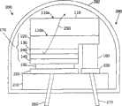
Referring now to Fig. 2, other embodiment of light-emitting diode according to an embodiment of the invention is shown.At Fig. 2, it is flip-chip that light-emitting diode 200 is shown, and perhaps, utilizesweld zone mounting bracket 210, for example heat sink on.Weldzone mounting bracket 210, uses conventional solder reflow technology, and this solder preform spare can be refluxed so thatohmic contact Other weld zone silicon carbide substrates 110, away frommounting bracket 210,diode region 170 are placed downwards, and be adjacent with mounting bracket 210.The Resistance (not shown) also can be included between corresponding ohmic contact 150,160 and the corresponding fusion welded zone 220,230.The Resistance can comprise nickel, nickel/vanadium and/or titanium/tungsten.Also can use other Resistance.
Also with reference to Fig. 2, shown inlight 250, the light that produces inactive area 130 enterssubstrate 110, goes out from first 110a of substrate 110.In order to make inactive area 130 light that producesenter substrate 110 easily, cancremasteric reflex device 240, it is betweenactive area 130 and themounting bracket 210, and is relative with substrate 110.Reflector 240 can be betweenactive area 130 and thep type layer 140, as shown in Figure 2.Yet, betweenreflector 240 andactive area 130 and/orp type layer 140, also one or more intermediate layers can be arranged.In addition,p type layer 140 can be betweenreflector 240 and the active area 130.Also can provide other structure, for example below in conjunction with as described in Figure 16.
Also with reference to Fig. 2, how shownexemplary light ray 250 explanations only begins to propagate along the direction of leavingsubstrate 110 if producing in theactive area 130, but is reflected bysubstrate 110 andleft device 200 by reflector 240.Notice that in the flip chip structure of Fig. 2 explanation,light 250 only needs once to propagate bysubstrate 110 before leaving device.
With reference to Fig. 3, by on first 110a ofsilicon carbide substrates 110, provide negative electrode ohmic contact 160 ', and negativeelectrode ohmic contact 160 on first 110a ' between providelead 390 or other to be electrically connected to external cathode lead-inwire 270, alsovertical LED 300 can be encapsulated in the flip chip structure.Also can provide non-inverted structure, for example, as below in conjunction with as described in Figure 16.
Fig. 4 illustrates other LED according to an embodiment of the invention.In these LED400, the anode contact can comprise ohm andecho area 410, and it can comprise a plurality of layers, comprises thin transparentohmic contact 412 and reflector 414.Thin transparentohmic contact 412 can comprise platinum, preferably should approach as far as possible to avoid sizable light absorption.The thickness of thin transparentohmic contact 412 forplatinum transparency electrode 412 preferably about 10 With about 100Between.In other embodiments, thin transparent
ohmic contact 412 can comprise nickel/gold, nickel oxide/gold, and nickel oxide/platinum, titanium and/or titanium/gold, having has thickness about 10With about 100Between.Reflector 414 preferably is thicker than about 300, and preferably include aluminium and/or silver.The embodiment of Fig. 4 can provide the current expansion of improvement, because theohmic contact 412 ofreflector 414 Contact Thin on the whole surface area of thin transparent ohmic contact 412.Therefore, as the situation in the conventional device, electric current does not need to contact 410 horizontal transmission by anode.Therefore, can strengthen current expansion.Thedevice 400 of Fig. 4 can resemble also that Fig. 2 and Fig. 3 go out encapsulate.Also can adopt other contact structures, for example, below in conjunction with Figure 16 and Figure 17 describe in detail like that.For example, for example comprise that theResistance 155 of nickel, nickel/vanadium and/or titanium/tungsten may be provided betweenreflector 414 and theweld zone 220 and betweenohmic contact 160 andweld zone 230.

Fig. 5 shows the LED according to other embodiments of the invention.Thereby these embodiment of LED500 can by to substrate 110 ' the 110c of partial sidewall at least form inclined-plane or inclination and strengthen light extraction from LED.Since irradiation rampedside walls 110c angle of light normally than other situation more near normal, fewer like this light can be reflected entersubstrate 110 '.Correspondingly, can be from substrate 110 ' extraction light, this can improve the gross efficiency of device.By use conventional method make substrate 110' sidewall 110c and/or first 110a roughening or form texture, can further improve extraction efficiency.
Correspondingly, comprise substrate according to the light-emitting diode of some embodiments of the present invention and based on the diode region of gallium nitride.Substrate comprises that transparent single-crystal silicon carbide is used for interested transmitting boundary, preferably prepares by sublimed method.Substrate can be the thickness between about 100 μ m and about 1000 μ m.Extract light owing to improved from substrate, the external efficiencies of diode can improve.In according to some embodiments of the present invention, diode comprises reflector, and it is used for extracting from device subsequently in the light reflected back substrate that produces in the diode region.Reflector can be included in the low relatively material (as AlGaN) of the active area last layer refractive index relative with substrate.As selection, reflector can be included in Bragg reflector and/or aluminium on transparent ohmic contact and/or the silver-colored coating in the structure.Below other embodiment will be described.In other embodiments, the part of substrate sidewall can be tapered and/or roughening to improve light extraction.Diode according to some embodiments of the present invention can be particularly suitable for using the flip-chip mounting structure.Yet, also can use non-flip-chip to install.
Embodiments of the invention by above-mentioned Fig. 1-6 description, the modification of silicon carbide substrates is provided, be used to extract the device of at least some light of the light of predetermined wavelength range with concrete enforcement, thereby allow the flip-chip of the gallium nitride based LED on carborundum or non-flip-chip to install.Describe other embodiments of the invention now, substrate has been made various geometric modification herein, to be provided for extracting other embodiment of the device of at least some light, to improve extraction efficiency from substrate.When making large-area chips, these substrate modification can be particularly suitables, to be provided for extracting from substrate other embodiment of the device of at least some light, allow from substrate interior district raising extraction efficiency.These raisings can be used with silicon carbide substrates, as top in conjunction with Fig. 1-6 together as described in, but also can be with comprising that GaAs, gallium phosphide, their alloy and/or sapphire conventional substrate use.
Fig. 7 A is the top view according to the LED of other embodiments of the invention.According to other embodiments of the invention, Fig. 7 B and Fig. 7 C are the sectional view of the LED of Fig. 7 A along theline 7B-7B ' among Fig. 7 A.
Referring now to Fig. 7 A-7C, these LED comprisesubstrate 710 and thediode region 740 on second 710b ofsubstrate 710 that the first and secondopposite face respectively.Substrate 710 for example can be, thesilicon carbide substrates 110 described in Fig. 1-6, and/or another kind of conventional LEDsubstrate.Diode region 740 can comprise thediode region 170 shown in top Fig. 1-5, and/or any other conventional diode region.
Also shown in Fig. 7 A, first 710a of these LED700 is comprising a plurality ofgrooves 720, and it has determined a plurality ofbearings 730 in substrate.In Fig. 7 A, show the triangle bearing.Yet, other polygon or non-polygonal bearing also can be provided.Shown in Fig. 7 B, groove 720 can comprise inclined-plane bottom 722.Yet, also can comprise the plane bottom.In addition, meet at right angles though 724 couples of first 710a of sidewall and second 710b of groove are shown, also can comprise tapered sidewalls, wherein the zone of the cross section of sidewall preferably reduces to second 710b from first 710a ofsubstrate 710.
Fig. 7 C shows other embodiment that the on-plane surface feature is provided.Therefore, can use wide saw cut or other technology with form bearing 730 ', this bearing 730 ' have taper andcrooked sidewall 724, crooked bottom 722 ' and/or at bearing 710 ' interior first 710a ' of cheese.Bearing 730 ' these embodiment can form lentiform structure thus, this can reduce total internal reflection.As selection, be better than first 710a ' of bending or lens shaped and/or bottom 722 ', can first 710a ' or bottom 722 ' on form facet, with further enhancing light extraction.Burn into saw cut, laser cutting and/or other routine techniques can be used to produce these structures.
At last, also shown in Fig. 7 A-7C, the circumference of first and second 710a, 710a ' and 710b is foursquare.Yet, should be appreciated that, can adopt other shape.For example, also can use first and second of triangle periphery shape.In addition,, also can use two or more bearings, preferably, have area for example greater than 0.1mm though show fourtriangle bearings 7302Big relatively chip in can use bearing more than four.
Fig. 8 A is the top view according to the LED of other embodiments of the invention.According to other embodiments of the present invention, Fig. 8 B and Fig. 8 C are that the LED of Fig. 8 A is along theline 8B-8B ' sectional view among Fig. 8 A.
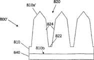
Shown in Fig. 8 A, these light-emittingdiodes 800 comprise thesubstrate 810 with the first and secondopposite face diode region 840 onsecond 810b.Substrate 810 can be a silicon carbide substrates, for example silicon carbide substrates of describing together in conjunction with Fig. 1-6 110, and/or any other common LEDsubstrate.Diode region 840 can be thediode region 170 based on gallium nitride described of Fig. 1-5 for example, and/or other any conventional diode region.
Shown in Fig. 8 A and Fig. 8 B,substrate 810 is included in the via-hole array 820 in first 810a.Preferably, throughhole 820 only extends throughsubstrate 810 part paths, but in other embodiments, they can extend throughsubstrate 810 whole paths.As shown in the figure, through hole can comprise tapered sidewalls 824.Sidewall 824 can be curved or rectilinear.In addition, also can use curve or straight sidewall perpendicular to first 810a and second 810b.Throughhole 820 can have flat, and inclined-plane and/orcrooked bottom 822 are to provide frustum of a cone shape (frusto-conical) or cylindrical hole.Through hole also can not comprise bottom 822, but arrives a point so that cone-shaped hole to be provided.Though, at the array of four complete through holes shown in Fig. 8 A and Fig. 8 B and 12 partial through holes, can use two or more than two throughhole 820, preferably, to area for example greater than 0.1mm2Large-area chips can comprise complete throughhole 820 more than four.
Shown in Fig. 8 B, first can be comprising first 810a of one or more faceted inclinations.In other embodiments,end face 810a can be by fillet to provide lentoid.
As to be described in detail below, thegroove 720 of Fig. 7 A-7C for example can use before or after diced chip with the slicing machine at the angle at 45, limit of chip and make.Can use other technology, comprise reactive ion etching, laser cutting, wet etching and/or other technology by mask.The throughhole 820 of Fig. 8 A-8C can use the reactive ion etching by mask to prepare before or after diced chip.
Light extraction by the LED of Fig. 7 A-7C and Fig. 8 A-8C is described now.Groove 720 or throughhole 820 can allow periodically to pass chip and light extraction occur, rather than only along the edge of chip.Therefore, they can provide the scalability (scalability) of large-area chips.Cutting substrate-like becomes obviously contrast in groove to allow with being located at the interior cutting groove of substrate for this, also forms obvious contrast with the groove that cuts by the diode region of LED.
Bearing, through hole, sidewall and/or groove can improve light extraction, because the vertical edges of chip works in light extraction usually.In addition, for the purpose of light extraction, the best shape of led chip may not be the square or rectangular circumference.Yet owing to packaging density in wafer, led chip has square perimeter usually.In square chip, from greater than critical angle and less than the light of any direction irradiation sidewall at the angle at the supplementary angle of this critical angle since internal reflection and absorption subsequently can lose usually.Cylindrical chip can reduce internal reflection, but their manufacturability and packaging density are not good.In addition, can increase at the light that produces from the point that is distal to cylindrical small pieces central authorities and produce tangentially and be radiated at light on the vertical sidewall.More rays is owing to internal reflection and absorb loss again.Thereby total die area need be bigger than active hub district area, and this makes that the chip area service efficiency is low and causes higher cost.
On the contrary, can in substrate, form bearing, for example equilateral or non-equilateral triangle bearing 730 according to some embodiments of the present invention.Can keep best wafer utilization.Particularly, the light of generation can have no more than incident and reflection once during greater than critical angle in angle on sidewall 724.Incidence angle greater than critical angle is reflected, and still, the incident ray in all situations is to shine next wall less than critical angle, and the refractive index of supposing encapsulant is about 1.5 or bigger.Therefore, be different from the small pieces of arc with right angle or smooth and continuous, light can total loss in internal reflection and absorption.
LED with triangle compares with the square LED that has same chip area and have smooth vertical sidewall to move under identical electric current, for example can produce 15% raising at the light output facet.In addition, tapered sidewalls or raceway groove can use so that obtain more capture light in substrate with the triangle bearing.At last, the triangle bearing that the cutting of the groove of use and square small pieces angle at 45 or other angle can form can allow to handle and isolation technics with the standard small pieces, and the advantage of the additional light extraction of non-square chip still can be provided.Also can use standard edge to be shaped separates with small pieces.Use via-hole array 820 that similar effect can be provided.
Be appreciated that the LED among Fig. 7 A-7C and Fig. 8 A-8C can be to be inverted or to install with inverted structure, as Fig. 2-5 explanation.Can prevent to be used for that LED is coupled to the silver epoxy that substrate is installed and enter groove or through hole, this may reduce its efficient.In other embodiments, if groove and/or through hole are installed use with the non-flip-chip LED of routine, reflected back layer (reflective back layer), for example silver or aluminium, can be formed on first of substrate, make the light that is incident on groove or the through hole reflect back and pass through diode region towards diode region.
Discuss adopting solder preform spare to provide additional in theweld zone 220/230 now.Small size LED can require especially carefully to avoid being used for silver epoxy contact chip sidewall and/or the conductive substrates of sticking small pieces to lead frame.This contact can form the Schottky diode, and this performance to the vertical LED structure is harmful to.The Schottky diode may be shunted near the electric current the LED, because it has lower forward to connect voltage.On big chip, use the silver epoxy can easier processing, because excessively disperse (over-dispensing) can not can to cause that epoxy resin exposes and may arrive the vertical sidewall of diode region and/or substrate below chip than on little chip.According to embodiments of the invention, solder preform spare can be formed on or adhere on reflector or other layer, and is as described below.Preformed member can comprise the low-temperature eutectic alloy, lead-Xi for example, indium-Jin, Jin-Xi, and/or silver-tin solder.The shape of preformed member can finely be determined, and can be controlled outside creep by working pressure and/or temperature in the small pieces adhesion process.In addition, the thermal conductivity of preformed member can be better than silver epoxy, and this is more favourable for high power device.
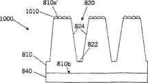
Referring now to Fig. 9 and Figure 10, also can provide substrate is carried out veining.Forming texture can be in emission wavelength or bigger magnitude.For example, as shown in Figure 9,LED 900 can comprise first 710a ' of the veining of substrate 710.Except or first 710a ' of alternative veining, can also provide thesidewall 724 of veining ' and/or thebottom 722 of veining '.As shown in figure 10,LED 1000 can comprise first 810a ' of veining, can comprisemicrolens array 1010 on first.The sidewall and/or the bottom of veining also can be provided.As case description, form texture and also can use with other example described herein in conjunction with Fig. 9-10.
To the preferably veining and not polishing of the exposed surface of encapsulated LED chip.Encapsulate on the epitaxial lateral of conventional chip with polishing, this can reduce light extraction therefrom.The veining of exposed surface can provide and make incident light by transmission and not by the random chance of internal reflection.Be appreciated that and do not hinder this substrate surface formation ohmic contact the substrate back veining.More particularly, vertical LED can have one with the contacting of active area, and have a back to contact with the substrate back of veining.Compare with polished surface, the sidewall of veining can provide and reach 20% or the emission of higher light.
Figure 11 and 12 shows other LED according to some embodiments of the present invention.The LED 1100 of Figure 11 and theLED 1200 of Figure 12 can be corresponding with theLED 800 of theLED 700 of Fig. 7 and Fig. 8.Yet, in the embodiment of Figure 11 and Figure 12, increased transparentohmic contact 412 and reflector 414.Thin transparentohmic contact 412 can improve the current expansion of p type gallium nitride layer, can produce ohmic contact by antianode, preferably stops the light quantity that reduces simultaneously, is more preferably to stop minimized light quantity.
In addition, in Figure 11 and structure shown in Figure 12, be installed in the chip of installing on thesubstrate 210 because chip is upside-down mounting, so transparentohmic contact 412 can be thinner than transparent ohmic contact possible in the conventional nitride LED, this just allows it more transparent.Thick relatively reflector 414 can be provided, andreflector 414 comprises for example aluminium and/orsilver.Reflector 414 can provide good current expansion.In addition, solder preform spare 220 and/or other installing zone can be used inMetal Contact 155 and install between thesubstrate 210 so that electricity and mechanical connection and the heat transfer with diode region to be provided, and avoid the short circuit in producing the diode region that will cause parasitic Schottky contact simultaneously.Be appreciated that and use flip-chip that diode is installed, power dissipation does not need to take place by substrate.And, produce heat diode region can with heat sink tight the contact, lower thermal resistance is arranged.In other embodiment that for example describes, can adopt non-flip chip structure to install in conjunction with Figure 16.Also be appreciated that transparent/reflector electrode, solder preform spare and/or flip-chip are installed and can be used with other embodiments of the invention described herein.
Figure 13 shows other embodiments of the invention of the extraction efficiency that can be used for improving conventional ATON LED.As known to a person skilled in the art, ATON LED uses substrate to be shaped, and is " OSRAM Enhances Brightness of Blue InGaNLEDs " at the title of publishing for example, Compound Semiconductor, Volume7, No.1,20012 months, p.7 as described in.Particularly, as shown in figure 13,conventional ATON LED 1300 comprisessubstrate 1310 and diode region 1320.According to embodiments of the invention, for example the emitter region that is limited bytable top 1320a and/or electrode 1330 only is included in the middle body of diode region, not in the peripheral portion of diode region not exceptionally.Electrode 1330 is transparency electrode preferably, can be littler thanemitter region 1320a with depositing the space with emitter region 1320a.Also can adopt other technology that is used to reduce the emitter region area.
In other words,substrate 1310 has first and secondopposite face 1310a and the1310b respectively.First 1310a has less surface area than secondface.Diode region 1320 is at second above the1310b.Emitter region 1320a is included in thediode region 1320, and is to be limited in the less surface region of first 1310a.This structure can make chip seem more to resemble point-source of light on the focus of lens.Usually, the light that produces at chip edge can not obtain more benefits of profiled edge, because compare with the light that produces in chip central authorities, littler light-emitting solid surface influences each other with those surfaces.Analog representation by from chip edge the emitter region being introduced, can obtain many 20% light output approximately.Improve extraction efficiency by reducing emission area, this also makes light output insensitive to the loss in the substrate and on substrate surface, because more light can be escaped when passing active area for the first time.The embodiment of Figure 13 can be used for conventional non-Flip-Chip Using.The embodiment that can be used for the ATON LED of Flip-Chip Using will describe in conjunction with Figure 17 below.
Figure 14 A explanation reduces the emitter region area and is applied to other embodiments of the invention.For example,LED 1400 is theLED 700 that are similar to Fig. 7, except at least one emission area that reduces is provided according to embodiments of the invention.The emission area that can provide at least one to reduce by one or moreconductive electrodes 1410 of aiming at bearing 730.Conductive electrode 1410 can comprise platinum and/or other material.The insulating barrier 1420 that for example comprises silicon nitride can be used for stoping the Metal Contact with diode region 740.Interconnectingmetal layer 1430 can be on theconductive electrode 1410 and the cover layer of formation on the silicon nitride layer 1420.Be appreciated thatinterconnection layer 1430 also can be used as the reflector.As selection, can provide one or more reflector that separate.Figure 14 B is the bottom view of the LED of Figure 14 A, showsconductive electrode 1410 and metal level 1430.Be appreciated that in other embodiments of the invention at least onetable top 1320a of Figure 13 can be included in thediode region 740 of Figure 14 A, with the emission area that provides at least one to reduce.In addition, the emission area that reduces can be used together with other embodiments of the invention described herein.
Therefore, can be by reducing the emitter region area so that more be limited to the efficient that improves LED in the middle body in back-welding shape district.For the back-welding shape device that even emission area is arranged, the chip lower with efficient becomes the district to compare the more emission of appearance.On the contrary, in Figure 14 A and Figure 14 B,, can provide the extraction efficiency of improvement because emitter region or a plurality of emitter region are aimed at bearing 730.Becauseconductive electrode 1410 is to disconnect mutually, so they need link to each other with interconnect conductive metal 1430.If device is the flip-chip combination, conductingmetal 1430 can be scolder and/or the epoxy resin of filling out silver.If device is mounted in the non-flip chip structure, can comprise that for example reflector bonding jumper and/or lead-in wire connect (wire bond) and be used for interconnection sheet metal.
Figure 15 A shows at least one emitting area that reduces and is applied to other embodiments of the invention.For example, except at least one emitting area that reduces was provided according to embodiments of the invention, LED1500 was similar to the LED800 of Fig. 8.The emitting area that can provide at least one to reduce by theconductive electrode 1510 that does not cover through hole 820.Conductive electrode 1510 can comprise platinum and/or other material.The insulatingbarrier 1520 that for example comprises silicon nitride can be used to stop the Metal Contact on the zone of being determined by through hole 820.Figure 15 B is the bottom view of the LED of Figure 15 A, showsconductive electrode 1510 and insulation layer 1520.As the situation of Figure 14 A, in other embodiments, thediode region 840 interior emitting areas to provide at least one to reduce of Figure 15 A can be provided at least onetable top 1320a of Figure 13.
Be appreciated that as described abovely, can use embodiments of the invention to improve based on sapphire nitride LED and based on the LED of other material system.Yet in based on sapphire nitride LED, most light can be captured in the nitride diode district of high index of refraction.Be higher than the carborundum of sapphire refractive index for the refractive index of substrate, gallium nitride, aluminium nitride, zinc oxide and/or other substrate can have bigger gain.Therefore, embodiments of the invention are not limited to use carborundum to be substrate.Be appreciated that when sapphire during as substrate, the sapphire insulating barrier can use two with the contacting of diode region, for example shown in Figure 1.These contact needs are aimed at the electrical connection in the encapsulation.If exposed side is polished, the transparency of Sapphire Substrate can help aiming at.Yet, the exposed surface of polishing and the surface ratio that forms texture, light extraction efficiency may be lower.
Figure 16 is the sectional view of light-emitting diode according to an embodiment of the invention.It is similar with Fig. 3 that Figure 16 can think, except light-emittingdiode 1600 is to be configured to that non-flip-chip is installed rather than flip-chip installs.In addition, also show other contact structures between LED and mounting bracket, for example installation component or sub-installation component.The non-flip-chip that is appreciated that Figure 16 installs and/or the contact structures of Figure 16 can be used with other embodiments of the invention described herein and/or other conventional LED.
More specifically, with reference to Figure 16, light-emittingdiode 1600 is to be installed on the mountingbracket 210 with non-flip chip orientation, and whereinsilicon carbide substrates 110 is adjacent with mountingbracket 210,diode region 170 be relative with mountingbracket 210 or away fromsilicon carbide substrates 110 above.In other words,diode region 170 up,silicon carbide substrates 110 is down.Have been found that according to the embodiments of the invention shown in Figure 16 when using transparentsilicon carbide substrates 110, the light quantity of extracting from the non-flip-chip mounted LEDs of routine can increase.In these embodiments, the light that enterssilicon carbide substrates 110 downwards that produces from theactive area 130 ofdiode region 170 is reflected bysilicon carbide substrates 110 by reflector 140.Though extraction efficiency may be littler than the LED300 among Fig. 3, can obtain the extraction efficiency bigger than the extraction efficiency of the conventional LED that does not adopt transparent silicon carbide substrates 110.Be appreciated that with adjacent transparent silicon carbide substrates of installing zone and facing up to install and also can use away from Figure 16 of the diode region of installing zone with other conventional LED structure.
Also,contact structures 1620 are according to an embodiment of the invention described with reference to Figure 16.Be appreciated that thesecontact structures 1620 can use with other embodiment described herein, also can use with other conventional LED structure.
As shown in figure 16,contact structures 1620 compriseohmic region 160,reflector 140,Resistance 1610 and weld zone 230.Topohmic contact 150 also is provided.Ohmic contact 150/160 is one or more layers metal hyaline layer preferably, Bao platinum layer for example, and its thickness can be about 10With 100Between.Can adopt other transparentohmic contact 150/160.For example, transparent oxide for example can adopt indium tin oxide (ITO), and the thickness ofohmic contact 150/160 in this case can be several microns orthicker.Ohmic contact 150/160 can be even thick layer, grid structure and/or dot structure, for example, as 5,917,202 descriptions of United States Patent (USP) of authorizing people such as Haitz, their content is herein incorporated by reference, as statement fully here.Ohmic contact 150/160 preferably provides current expansion, effectively and evenly is injected intoactive area 170 to help electric current.When grid structure or dot structure are used forohmic contact 150/160, ifsilicon carbide substrates 110 has suitable coupling conductivity, current expansion can realize.Because the area that reduces covers, a grid/ohmic region can reduce or minimize the light absorption in the ohmic region.Be appreciated thatohmic contact 150 does not need identical with 160 structure.
Also with reference to Figure 16,reflector 140 can comprise for example about 100With about 5000Between reflective metals, for example silver and/or aluminium, and/or Jing Dui (mirrorstack) as has been described.The function that also is appreciated thatohmic region 160 andreflector 140 can be merged into single ohm and reflector area, and for example single silver or aluminium can provide current expansion and reflection function simultaneously.Alternatively, can use different layers asohmic region 160 andreflector 140.
Also with reference to Figure 16, also can provideResistance 1610, diffusion and/or spike that itsprotection reflector 140 and/orohmic region 160 are avoided adhering to from following small pieces form.Therefore the light and/or the electric integrality ofohmic region 160 and/orreflector 140 can be protected in Resistance 1610.At some embodiment, the Resistance is included in about 100With about 5000Between nickel nickel/vanadium and/or titanium/tungsten.
At last, also with reference to Figure 16, provideweld zone 230 to be used to adhere to the semiconductor LED structure to mountingbracket 210, for example an installation component or sub-installationcomponent.Weld zone 230 can be for example to comprise gold, indium, and scolder, and/or the metal level of brazing, and can comprise one or more preformed members of these and/or other structure.In certain embodiments,weld zone 230 can comprise pedestal (solder bump) and/or other metal salient point, for example indium orgold.Mounting bracket 210 can comprise heat sink, surface mounting technology (Surface MountTechnology (SMT)) encapsulation, and printed substrate, driver IC, lead frame and/or other are used for conventional installation component and/or the sub-installation component ofLED.Weld zone 230 can be adhered to mountingbracket 210, uses silver epoxy, scolder welding, hot weld welding and/or other technology.The embodiment that is appreciated that thecontact structures 1620 of Figure 16 can use with flip-chip LED and/or other conventional LED structure.
Figure 17 A is the sectional view according to the light-emitting diode of other embodiments of the invention.Particularly, Figure 17 A illustrates conventional ATON LED, and one it be that contact structures are according to an embodiment of the invention installed and/or used to flip-chip.Can use flip-chip to install, for example shown in Figure 2, and/or contact structures, for example Figure 16 explanation.
Referring now to Figure 17 A, these embodiment of LED1700 comprisetransparent substrates 1310, silicon carbide substrates for example colourless, compensation, withdiode region 1320, it is that flip-chip is installed on the mountingbracket 210, make thatdiode region 1320 is adjacent with mountingbracket 210, andsilicon carbide substrates 1310 is away from mounting bracket210.Diode region 1320 can comprise the emitting area that reduces, for example themesa region 1320a of Figure 13.
Flip-chip shown in Figure 17 A is installed with the non-flip-chip installation LED of routine and is compared, and the light extraction of improvement can be provided.For example, in the conventional chip in the gallium nitride district on using silicon carbide substrates, can actual transmission go out at inner the only about half of of light that produce of LED active area.Because total internal reflection and/or absorption loss water, remaining light can be trapped in the semi-conducting material.Wherein first surface area ratio silicon carbide substrates second the little this structure adjacent with diode region away from the silicon carbide substrates of diode region can improve light extraction.Yet radiative major part is incident light and/or the chip face that passes through and/or part covering complete with the absorption metal, helps the ohmic contact to LED p district and n district.In addition, below conventional LED at first guided light into, this can cause the extra reflection and/or because the loss of small pieces adhesion material of the optical element in the LED encapsulation.These phenomenons can cause extra optical loss.
Obviously opposite, embodiments of the invention as Figure 17 A explanation can use ATON geometry and/or other geometry, it comprises compares first 1310a that has reduced area with second 1310b, it is to be installed to mountingbracket 210 so thatdiode region 1320 is adjacent with mountingbracket 210 with flip chip, andsubstrate 1310 is away from mountingbracket 210.
In addition, also shown in Figure 17 A, use ptype contact structures 1740 can obtain extra efficient, this structure comprises ptype ohmic region 1742,reflector 1744,Resistance 1746 and/or weld zone 1748.In certain embodiments, p typeohmic region 1742 can comprise p type ohmic metal, nickel/gold for example, and nickel oxide/gold, nickel oxide/platinum, titanium and/or titanium/gold, thickness is about 10With about 100Between.In certain embodiments, p typeohmic region 1742 can comprise continuous or discontinuous p type ohmic metal, and area covers between about 10% to about 100%, and thickness is about 2To about 100Between.To discrete p type ohmic metal, the conductivity of following diode layer can cover coupling with area, to improve the uniformity of electric current injection diode active area.
Also with reference to Figure 17 A, for example thethick reflector 1744 of silver and/or aluminium is onohmic region 1742, and is relative with diode region 1320.In other embodiments,ohmic region 1742 can be enough thick so that contact resistance is low, but enough thin to reduce lightabsorption.Ohmic region 150 can be equal to or less than half of ohmic metal thickness of conventional ATON chip, to adapt to the doubling by this contact of light.In addition, can present the current expansion function by merging ohm and reflector area, ohm of merging and reflector area can be designed to enough thick, to promote effective optical reflection of thediode region 1320 interior light that produce, provide current expansion simultaneously.Therefore, the light 1726 that produces indiode region 1320 can reflect and leavereflector 1742, gets back in the substrate 1310.Other light 1722 that produces in diode region can directly inject in the substrate 1310.There is other light 1724 to go again from the sloped sidewall ejaculation of substrate.
Also with reference to Figure 17 A, the flip-chip mounted LEDs can be the small pieces that adoptweld zone 1748 to paste, and the weld zone comprises gold, indium, conventional epoxide resin material, brazing and/or scolder, and with suitable scolder and/orsolder stop district 1746 nickel for example, nickel/vanadium and/or titanium tungsten use together.Optional adhesion layer comprises for example titanium, also may be provided betweenbarrier layer 1746 and the weld zone 1748.Also be appreciated that by cremasteric reflex metal on semiconductor surface, can obtain very smooth mirror surface, it is compared with the relative rough surface of head has high relatively reflectivity.
Also with reference to Figure 17 A, can use ntype contact structures 1730, it comprises ohm/reflector area 1732,attachment zone 1734,Resistance 1736 and weld zone 1738.Ohm/reflector area 1732 can comprise n type ohmic material, for example aluminium and/or silver, about 1000Thick.This ohm/reflector area 1732 can be used as ohmic contact and reflector layer.The selectable optional reflector area that is similar toreflector area 1724 also can be provided.Optional attachment zone 1734 also can be provided, comprise for example about 1000Titanium.Also can provide Resistance 1736.For example also can use about 1000Platinum.At last, also can use weld zone 1738.For example, can use to reach 1 μ m or thicker gold, conventional lead-in wire connects 1750 can be attached to weld zone 1738.Be appreciated that according to specific application the one or more districts in thedistrict
According to the embodiment of Figure 17 A, flip-chip is installed the ATON chip and is compared the amount of radiation that can produce about 1.5 to 1.7 times or bigger raising with the non-flip-chip ATON of routine geometry.Can reduce the absorption in p type electrode and/or small pieces adhesion material.Can use ntype contact structures 1730, to reduce or the minimum surface covering.Therefore, in certain embodiments,electrode structure 1730 can occupy whole first 1310a of silicon carbide substrates 1310.Yet other geometry also can use to reduce or the minimum surface covering.
For example, shown in Figure 17 B, ntype contact structures 1730 can only be included in firstmiddle body 1730a on the 1310a.Yet to bigger chip size, thefinger 1730b of ntype contact structures 1730 also can be used to provide extra current expansion.Therefore, ntype contact structures 1730 can occupy first 1310 Zone Full.In other embodiments, occupying the zone can be less than Zone Full, and still occupying the zone can be greater than 10% of Zone Full.In a further embodiment, can use less than zone 10% area.Be appreciated that a lot of other geometrical forms that also can adoptmiddle body 1730a and refer to 1730b.
In order to improve scalability, ntype contact structures 1730 can be a kind of grid structures of interconnection, aspect surface coverage and current expansion resistance with belowsemi-conducting material 1310 conductivity be complementary.By reducing and preferably minimizing the surface coverage of ntype contact structures 1730 and use silver and/oraluminium reflector 1732, can reduce and preferably minimize the absorption of whole ntype contact structures 1730.
Be appreciated that in other embodiments n type and p type electrode can be formed on chip sides, as it is described like that to authorize the United States Patent (USP) 5,952,681 of Chen.This can further reduce the interior light absorption of ohmic contact of n electrode.
The flip-chip installation and/or the contact structures that are appreciated that Figure 17 A and Figure 17 B can have first the substrate geometry that reduces area to comprise cube with other, triangle, and pyramid, truncated pyramid and/or hemisphere are used together.As has been described, can provide patterned additional first with groove, through hole and/or other pattern characteristics form.At last, as has been described, also can use veining and/or roughening.Also can use the roughening of substrate and/or diode region.Therefore,reflector 1744 can be formed on and have a mind to form on thediode region 1320 of coarse and/or formation pattern.This random rough performance enough improves light extraction and/or reduces internal reflection.Concrete pattern is the Fresnel lens for example, also can be used to aim at reverberation and/or improve light extraction.Incase use reflector 1744, graphically can form optical element.The size of pattern can be the magnitude of the light wavelength sent from LED.
Figure 18 is the sectional view according to the light-emitting diode of other embodiments of the invention.Particularly, Figure 18 shows conventional ATON LED, is included in the reflector on its diode region.According to other embodiments of the invention, find unexpectedly, by adding upper reflector at the ATON that faces up of routine and/or the diode region of other LED, compare with the conventional ATON and/or the LED that on the diode region at its top surface place, do not have reflector, can increase about 10% or more brightness.Therefore, stop top surface, in fact can increase the light emission with reflector to small part.
More particularly, with reference to Figure 18, according to any embodiment described herein and/or according to the ATON of routine and/or other LED structure, theseLED 1800comprise substrate 1310 and diode region 1320.According to the ATON of routine and/or other structure, can provide n type contact structures 1810.As selection, ntype contact structures 1810 can be provided, it comprises anattachment zone 1812, for example about 1000Titanium, aResistance 1814, for example about 1000Platinum and aweld zone 1816, the gold of for example about 1 μm.Attachment zone 1812 can additionally be reflexive also as ohmic contact also.
Also, can provide ptype contact structures 1820 with reference to Figure 18.Ptype contact structures 1820 comprise transparentohmic district 1830, and it can be similar with theohm layer 1742 of Figure 17 A.Also can compriseadhesion layer 1826, it can be similar with theadhesion layer 1734 of Figure 17 A.Also can comprisebarrier layer 1824, it can be similar with thebarrier layer 1736 of Figure 17 A.Also can compriseweld zone 1822 and lead 1840,weld zone 1822 is similar with theweld zone 1738 of Figure 17 A, and lead 1840 is similar with thelead 1750 of Figure 17 A.In addition, also can provide conventional ATON/ITP ohmic contact structure.According to some embodiments of the present invention, ptype contact structures 1820 are used for light is reflected back comprising reflector 1828, bydiode region 1320 and enter substrate 1310.Reflector 1828 can be similar to thereflector 1746 of Figure 17 A.As mentioned above, unexpectedly,, for example be between about 1.2 of conventional ATON LED brightness is arrived about 1.3 times or bigger by increasing brightness on the top surface that reflector 1828 is added to ATON and/or other LED.
Referring now to Figure 19, the LED manufacture method according to the embodiment of the invention will be described.Some pieces that are appreciated that Figure 19 can occur with the shown different order of figure, and some pieces can be carried out simultaneously rather than order is carried out.
With reference to the piece 1910 of Figure 19, diode region is formed on the silicon carbide substrates.As mentioned above, preferably, the gallium nitride diode district is produced on the silicon carbide substrates.At piece 1920, as in conjunction with Fig. 7-12 and Figure 14-15 together as described in, groove can pass through saw, burn into laser cutting, reactive ion etching, wet etching and/or other cutting method, and/or carries out reactive ion etching so that form through hole on first of substrate.Be appreciated that before making diode region on the substrate and/or on substrate and after the making diode region, can form groove and/or through hole at piece 1920.
Reference block 1930 for example in conjunction with as described in Fig. 2-5, Figure 11-12 and Figure 16-17, forms contact structures.Be appreciated that before the formation groove of piece 1920 and/or reactive ion etching through hole and can form contact structures.
Reference block 1940 is carried out cutting to separate single led chip.Be appreciated that if make the LED of wafer size, then do not need to carry out cutting, and, can carry out diced chip before the formation electrode structure of piece 1930 and/or before the kerf and/or reactive ion etching at piece 1920.
Reference block 1950 then, for example adopt solder preform spare and/or other interconnection technique, and as described in conjunction with Fig. 2-5, Figure 11-12 and Figure 16-17, diode is connected to mounting bracket.At piece 1960, diode for example is encapsulated in the plastic dome, as Fig. 2-3 and illustrated in fig. 16.Therefore can make LED effectively with high extracting efficiency.
In accompanying drawing and explanation, typical preferred embodiment of the present invention is disclosed, though used particular term, they only use on general and descriptive sense, rather than for the restriction purpose, scope of the present invention proposes in following claim.
Claims (52)
Translated fromChinesePriority Applications (1)
| Application Number | Priority Date | Filing Date | Title |
|---|---|---|---|
| CN201410858576.1ACN104835886A (en) | 2001-02-01 | 2002-02-01 | Light emitting diodes including modifications for light extraction and manufacturing methods therefor |
Applications Claiming Priority (4)
| Application Number | Priority Date | Filing Date | Title |
|---|---|---|---|
| US26570701P | 2001-02-01 | 2001-02-01 | |
| US60/265,707 | 2001-02-01 | ||
| US30723501P | 2001-07-23 | 2001-07-23 | |
| US60/307,235 | 2001-07-23 |
Related Child Applications (2)
| Application Number | Title | Priority Date | Filing Date |
|---|---|---|---|
| CN201410858576.1ADivisionCN104835886A (en) | 2001-02-01 | 2002-02-01 | Light emitting diodes including modifications for light extraction and manufacturing methods therefor |
| CN200911000311.3ADivisionCN101976717B (en) | 2001-02-01 | 2002-02-01 | Light emitting diodes including modifications for light extraction and manufacturing methods therefor |
Publications (2)
| Publication Number | Publication Date |
|---|---|
| CN1552103A CN1552103A (en) | 2004-12-01 |
| CN100524848Ctrue CN100524848C (en) | 2009-08-05 |
Family
ID=26951384
Family Applications (3)
| Application Number | Title | Priority Date | Filing Date |
|---|---|---|---|
| CNB028044177AExpired - LifetimeCN100524848C (en) | 2001-02-01 | 2002-02-01 | Light emitting diodes including light extraction modifications and methods of making the same |
| CN201410858576.1APendingCN104835886A (en) | 2001-02-01 | 2002-02-01 | Light emitting diodes including modifications for light extraction and manufacturing methods therefor |
| CN200911000311.3AExpired - LifetimeCN101976717B (en) | 2001-02-01 | 2002-02-01 | Light emitting diodes including modifications for light extraction and manufacturing methods therefor |
Family Applications After (2)
| Application Number | Title | Priority Date | Filing Date |
|---|---|---|---|
| CN201410858576.1APendingCN104835886A (en) | 2001-02-01 | 2002-02-01 | Light emitting diodes including modifications for light extraction and manufacturing methods therefor |
| CN200911000311.3AExpired - LifetimeCN101976717B (en) | 2001-02-01 | 2002-02-01 | Light emitting diodes including modifications for light extraction and manufacturing methods therefor |
Country Status (10)
| Country | Link |
|---|---|
| US (6) | US6791119B2 (en) |
| EP (1) | EP1382073B1 (en) |
| JP (2) | JP2004521494A (en) |
| KR (1) | KR100643094B1 (en) |
| CN (3) | CN100524848C (en) |
| AU (1) | AU2002245361A1 (en) |
| CA (2) | CA2769808A1 (en) |
| MY (1) | MY127500A (en) |
| TW (1) | TW541715B (en) |
| WO (1) | WO2002061847A2 (en) |
Families Citing this family (546)
| Publication number | Priority date | Publication date | Assignee | Title |
|---|---|---|---|---|
| WO2001088917A1 (en)* | 2000-05-19 | 2001-11-22 | Matsushita Electric Industrial Co., Ltd. | Data recording medium and reproducing apparatus thereof |
| JP2002222992A (en)* | 2001-01-25 | 2002-08-09 | Rohm Co Ltd | LED light emitting element and LED light emitting device |
| US6794684B2 (en)* | 2001-02-01 | 2004-09-21 | Cree, Inc. | Reflective ohmic contacts for silicon carbide including a layer consisting essentially of nickel, methods of fabricating same, and light emitting devices including the same |
| US6791119B2 (en)* | 2001-02-01 | 2004-09-14 | Cree, Inc. | Light emitting diodes including modifications for light extraction |
| US6958497B2 (en)* | 2001-05-30 | 2005-10-25 | Cree, Inc. | Group III nitride based light emitting diode structures with a quantum well and superlattice, group III nitride based quantum well structures and group III nitride based superlattice structures |
| TWI294699B (en)* | 2006-01-27 | 2008-03-11 | Epistar Corp | Light emitting device and method of forming the same |
| US6787435B2 (en)* | 2001-07-05 | 2004-09-07 | Gelcore Llc | GaN LED with solderable backside metal |
| US7067849B2 (en) | 2001-07-17 | 2006-06-27 | Lg Electronics Inc. | Diode having high brightness and method thereof |
| US7211833B2 (en) | 2001-07-23 | 2007-05-01 | Cree, Inc. | Light emitting diodes including barrier layers/sublayers |
| US6747298B2 (en)* | 2001-07-23 | 2004-06-08 | Cree, Inc. | Collets for bonding of light emitting diodes having shaped substrates |
| US6740906B2 (en)* | 2001-07-23 | 2004-05-25 | Cree, Inc. | Light emitting diodes including modifications for submount bonding |
| JP4055503B2 (en)* | 2001-07-24 | 2008-03-05 | 日亜化学工業株式会社 | Semiconductor light emitting device |
| TW567619B (en)* | 2001-08-09 | 2003-12-21 | Matsushita Electric Industrial Co Ltd | LED lighting apparatus and card-type LED light source |
| DE10148227B4 (en)* | 2001-09-28 | 2015-03-05 | Osram Opto Semiconductors Gmbh | Radiation-emitting semiconductor chip, method for its production and radiation-emitting component |
| US6949395B2 (en) | 2001-10-22 | 2005-09-27 | Oriol, Inc. | Method of making diode having reflective layer |
| US7148520B2 (en) | 2001-10-26 | 2006-12-12 | Lg Electronics Inc. | Diode having vertical structure and method of manufacturing the same |
| US7858403B2 (en) | 2001-10-31 | 2010-12-28 | Cree, Inc. | Methods and systems for fabricating broad spectrum light emitting devices |
| US20030090103A1 (en)* | 2001-11-09 | 2003-05-15 | Thomas Becker | Direct mailing device |
| US7638346B2 (en) | 2001-12-24 | 2009-12-29 | Crystal Is, Inc. | Nitride semiconductor heterostructures and related methods |
| US8545629B2 (en) | 2001-12-24 | 2013-10-01 | Crystal Is, Inc. | Method and apparatus for producing large, single-crystals of aluminum nitride |
| US20060005763A1 (en) | 2001-12-24 | 2006-01-12 | Crystal Is, Inc. | Method and apparatus for producing large, single-crystals of aluminum nitride |
| US6635503B2 (en)* | 2002-01-28 | 2003-10-21 | Cree, Inc. | Cluster packaging of light emitting diodes |
| JP2003282939A (en)* | 2002-03-26 | 2003-10-03 | Oki Degital Imaging:Kk | Semiconductor light emitting device and method of manufacturing the same |
| US8294172B2 (en)* | 2002-04-09 | 2012-10-23 | Lg Electronics Inc. | Method of fabricating vertical devices using a metal support film |
| US6841802B2 (en) | 2002-06-26 | 2005-01-11 | Oriol, Inc. | Thin film light emitting diode |
| CA2492249A1 (en) | 2002-07-22 | 2004-01-29 | Cree, Inc. | Light emitting diode including barrier layers and manufacturing methods therefor |
| ATE500616T1 (en)* | 2002-08-29 | 2011-03-15 | Seoul Semiconductor Co Ltd | LIGHT EMITTING COMPONENT WITH LIGHT EMITTING DIODES |
| US10340424B2 (en) | 2002-08-30 | 2019-07-02 | GE Lighting Solutions, LLC | Light emitting diode component |
| KR101182041B1 (en)* | 2002-09-19 | 2012-09-11 | 크리 인코포레이티드 | Phosphor-coated light emitting diodes including tapered sidewalls, and fabrication methods therefor |
| JP4116387B2 (en)* | 2002-09-30 | 2008-07-09 | 株式会社東芝 | Semiconductor light emitting device |
| US7592636B2 (en) | 2002-09-30 | 2009-09-22 | Osram Opto Semiconductors Gmbh | Radiation-emitting semiconductor component and method for the production thereof |
| US7009199B2 (en)* | 2002-10-22 | 2006-03-07 | Cree, Inc. | Electronic devices having a header and antiparallel connected light emitting diodes for producing light from AC current |
| AU2003280878A1 (en)* | 2002-11-16 | 2004-06-15 | Lg Innotek Co., Ltd | Light emitting device and fabrication method thereof |
| US6943377B2 (en)* | 2002-11-21 | 2005-09-13 | Sensor Electronic Technology, Inc. | Light emitting heterostructure |
| DE60311678T2 (en)* | 2002-12-20 | 2007-11-22 | Cree, Inc. | METHOD FOR PRODUCING SEMICONDUCTOR DEVICES WITH MESASTRUCTURES AND MULTIPLE PASSIVATION LAYERS AND RELATED DEVICES |
| JP4254266B2 (en)* | 2003-02-20 | 2009-04-15 | 豊田合成株式会社 | LIGHT EMITTING DEVICE AND LIGHT EMITTING DEVICE MANUFACTURING METHOD |
| KR20050113200A (en) | 2003-02-26 | 2005-12-01 | 크리, 인코포레이티드 | Composite white light source and method for fabricating |
| TWI243488B (en)* | 2003-02-26 | 2005-11-11 | Osram Opto Semiconductors Gmbh | Electrical contact-area for optoelectronic semiconductor-chip and its production method |
| KR100964399B1 (en)* | 2003-03-08 | 2010-06-17 | 삼성전자주식회사 | Semiconductor laser diode and semiconductor laser diode assembly using same |
| US6885033B2 (en)* | 2003-03-10 | 2005-04-26 | Cree, Inc. | Light emitting devices for light conversion and methods and semiconductor chips for fabricating the same |
| US7141828B2 (en)* | 2003-03-19 | 2006-11-28 | Gelcore, Llc | Flip-chip light emitting diode with a thermally stable multiple layer reflective p-type contact |
| US7358539B2 (en)* | 2003-04-09 | 2008-04-15 | Lumination Llc | Flip-chip light emitting diode with indium-tin-oxide based reflecting contacts |
| US6831302B2 (en)* | 2003-04-15 | 2004-12-14 | Luminus Devices, Inc. | Light emitting devices with improved extraction efficiency |
| US7521854B2 (en)* | 2003-04-15 | 2009-04-21 | Luminus Devices, Inc. | Patterned light emitting devices and extraction efficiencies related to the same |
| US7105861B2 (en)* | 2003-04-15 | 2006-09-12 | Luminus Devices, Inc. | Electronic device contact structures |
| US20040259279A1 (en)* | 2003-04-15 | 2004-12-23 | Erchak Alexei A. | Light emitting device methods |
| US7262550B2 (en)* | 2003-04-15 | 2007-08-28 | Luminus Devices, Inc. | Light emitting diode utilizing a physical pattern |
| US7667238B2 (en)* | 2003-04-15 | 2010-02-23 | Luminus Devices, Inc. | Light emitting devices for liquid crystal displays |
| US7211831B2 (en)* | 2003-04-15 | 2007-05-01 | Luminus Devices, Inc. | Light emitting device with patterned surfaces |
| US7166871B2 (en)* | 2003-04-15 | 2007-01-23 | Luminus Devices, Inc. | Light emitting systems |
| US7098589B2 (en) | 2003-04-15 | 2006-08-29 | Luminus Devices, Inc. | Light emitting devices with high light collimation |
| US7074631B2 (en)* | 2003-04-15 | 2006-07-11 | Luminus Devices, Inc. | Light emitting device methods |
| US7084434B2 (en)* | 2003-04-15 | 2006-08-01 | Luminus Devices, Inc. | Uniform color phosphor-coated light-emitting diode |
| US7083993B2 (en)* | 2003-04-15 | 2006-08-01 | Luminus Devices, Inc. | Methods of making multi-layer light emitting devices |
| US7274043B2 (en)* | 2003-04-15 | 2007-09-25 | Luminus Devices, Inc. | Light emitting diode systems |
| US20040211972A1 (en)* | 2003-04-22 | 2004-10-28 | Gelcore, Llc | Flip-chip light emitting diode |
| US7531380B2 (en) | 2003-04-30 | 2009-05-12 | Cree, Inc. | Methods of forming light-emitting devices having an active region with electrical contacts coupled to opposing surfaces thereof |
| CA2523544A1 (en) | 2003-04-30 | 2004-11-18 | Cree, Inc. | High powered light emitter packages with compact optics |
| US7714345B2 (en) | 2003-04-30 | 2010-05-11 | Cree, Inc. | Light-emitting devices having coplanar electrical contacts adjacent to a substrate surface opposite an active region and methods of forming the same |
| US7087936B2 (en)* | 2003-04-30 | 2006-08-08 | Cree, Inc. | Methods of forming light-emitting devices having an antireflective layer that has a graded index of refraction |
| US7005679B2 (en) | 2003-05-01 | 2006-02-28 | Cree, Inc. | Multiple component solid state white light |
| US7528421B2 (en)* | 2003-05-05 | 2009-05-05 | Lamina Lighting, Inc. | Surface mountable light emitting diode assemblies packaged for high temperature operation |
| US7633093B2 (en)* | 2003-05-05 | 2009-12-15 | Lighting Science Group Corporation | Method of making optical light engines with elevated LEDs and resulting product |
| US7777235B2 (en)* | 2003-05-05 | 2010-08-17 | Lighting Science Group Corporation | Light emitting diodes with improved light collimation |
| WO2004102686A1 (en)* | 2003-05-09 | 2004-11-25 | Cree, Inc. | Led fabrication via ion implant isolation |
| JP3737494B2 (en)* | 2003-06-10 | 2006-01-18 | 株式会社東芝 | Semiconductor light emitting device, method for manufacturing the same, and semiconductor light emitting device |
| JP3813599B2 (en)* | 2003-06-13 | 2006-08-23 | ローム株式会社 | Method for manufacturing white light emitting diode element |
| US7211835B2 (en)* | 2003-07-09 | 2007-05-01 | Nichia Corporation | Light emitting device, method of manufacturing the same and lighting equipment |
| TWI312582B (en)* | 2003-07-24 | 2009-07-21 | Epistar Corporatio | Led device, flip-chip led package and light reflecting structure |
| US20050104072A1 (en) | 2003-08-14 | 2005-05-19 | Slater David B.Jr. | Localized annealing of metal-silicon carbide ohmic contacts and devices so formed |
| WO2005018008A1 (en)* | 2003-08-19 | 2005-02-24 | Nichia Corporation | Semiconductor device |
| EP1658642B1 (en)* | 2003-08-28 | 2014-02-26 | Panasonic Corporation | Semiconductor light emitting device, light emitting module, lighting apparatus, display element and manufacturing method of semiconductor light emitting device |
| US7029935B2 (en)* | 2003-09-09 | 2006-04-18 | Cree, Inc. | Transmissive optical elements including transparent plastic shell having a phosphor dispersed therein, and methods of fabricating same |
| US7183587B2 (en) | 2003-09-09 | 2007-02-27 | Cree, Inc. | Solid metal block mounting substrates for semiconductor light emitting devices |
| US7501669B2 (en) | 2003-09-09 | 2009-03-10 | Cree, Inc. | Wide bandgap transistor devices with field plates |
| JP2005117020A (en)* | 2003-09-16 | 2005-04-28 | Stanley Electric Co Ltd | Gallium nitride compound semiconductor device and manufacturing method thereof |
| WO2005029185A2 (en)* | 2003-09-16 | 2005-03-31 | Matsushita Electric Industrial Co., Ltd. | Led lighting source and led lighting apparatus |
| US7344903B2 (en)* | 2003-09-17 | 2008-03-18 | Luminus Devices, Inc. | Light emitting device processes |
| US7341880B2 (en)* | 2003-09-17 | 2008-03-11 | Luminus Devices, Inc. | Light emitting device processes |
| US7915085B2 (en) | 2003-09-18 | 2011-03-29 | Cree, Inc. | Molded chip fabrication method |
| JP2007521635A (en)* | 2003-09-19 | 2007-08-02 | ティンギ テクノロジーズ プライベート リミテッド | Semiconductor device manufacturing |
| US20080210970A1 (en)* | 2003-09-19 | 2008-09-04 | Tinggi Technologies Private Limited | Fabrication of Conductive Metal Layer on Semiconductor Devices |
| KR100799857B1 (en)* | 2003-10-27 | 2008-01-31 | 삼성전기주식회사 | Electrode structure and semiconductor light emitting device having same |
| JP4334321B2 (en)* | 2003-11-05 | 2009-09-30 | シャープ株式会社 | Manufacturing method of nitride semiconductor light emitting diode chip |
| JP3979378B2 (en)* | 2003-11-06 | 2007-09-19 | 住友電気工業株式会社 | Semiconductor light emitting device |
| US20050194584A1 (en)* | 2003-11-12 | 2005-09-08 | Slater David B.Jr. | LED fabrication via ion implant isolation |
| WO2005048364A1 (en)* | 2003-11-12 | 2005-05-26 | Cree, Inc. | Light emitting devices with self aligned ohmic contact and methods of fabricating same |
| EP1690301B1 (en)* | 2003-11-12 | 2012-08-15 | Cree, Inc. | Methods of processing semiconductor wafer backsides having light emitting diodes (leds) thereon |
| US20050104078A1 (en)* | 2003-11-13 | 2005-05-19 | Ite Compound Semiconductor Corporation | Light-emitting diode having chemical compound based reflective structure |
| KR100647279B1 (en)* | 2003-11-14 | 2006-11-17 | 삼성전자주식회사 | Nitride-based light emitting device and its manufacturing method |
| WO2005053000A2 (en)* | 2003-11-24 | 2005-06-09 | Tyco Electronics Corporation | Encapsulated gaas - based laser devices |
| US7518158B2 (en)* | 2003-12-09 | 2009-04-14 | Cree, Inc. | Semiconductor light emitting devices and submounts |
| US7450311B2 (en) | 2003-12-12 | 2008-11-11 | Luminus Devices, Inc. | Optical display systems and methods |
| US20050133806A1 (en)* | 2003-12-17 | 2005-06-23 | Hui Peng | P and N contact pad layout designs of GaN based LEDs for flip chip packaging |
| US7615689B2 (en)* | 2004-02-12 | 2009-11-10 | Seminis Vegatable Seeds, Inc. | Methods for coupling resistance alleles in tomato |
| JP2005228924A (en)* | 2004-02-13 | 2005-08-25 | Toshiba Corp | Semiconductor light emitting device |
| JP2005268275A (en)* | 2004-03-16 | 2005-09-29 | Sanyo Electric Co Ltd | Nitride based semiconductor light emitting diode element |
| JP2006066868A (en) | 2004-03-23 | 2006-03-09 | Toyoda Gosei Co Ltd | Solid element and solid element device |
| US7202181B2 (en) | 2004-03-26 | 2007-04-10 | Cres, Inc. | Etching of substrates of light emitting devices |
| US7355284B2 (en) | 2004-03-29 | 2008-04-08 | Cree, Inc. | Semiconductor light emitting devices including flexible film having therein an optical element |
| US7326583B2 (en) | 2004-03-31 | 2008-02-05 | Cree, Inc. | Methods for packaging of a semiconductor light emitting device |
| US7279346B2 (en)* | 2004-03-31 | 2007-10-09 | Cree, Inc. | Method for packaging a light emitting device by one dispense then cure step followed by another |
| US7517728B2 (en)* | 2004-03-31 | 2009-04-14 | Cree, Inc. | Semiconductor light emitting devices including a luminescent conversion element |
| US7419912B2 (en)* | 2004-04-01 | 2008-09-02 | Cree, Inc. | Laser patterning of light emitting devices |
| US7868343B2 (en)* | 2004-04-06 | 2011-01-11 | Cree, Inc. | Light-emitting devices having multiple encapsulation layers with at least one of the encapsulation layers including nanoparticles and methods of forming the same |
| EP1756875A4 (en)* | 2004-04-07 | 2010-12-29 | Tinggi Technologies Private Ltd | FABRICATION OF A RETROFLECTIVE LAYER ON SEMICONDUCTOR ELECTROLUMINESCENT DIODES |
| KR100549219B1 (en)* | 2004-04-12 | 2006-02-03 | 한국전자통신연구원 | Silicon light emitting device and manufacturing method thereof |
| US7064356B2 (en) | 2004-04-16 | 2006-06-20 | Gelcore, Llc | Flip chip light emitting diode with micromesas and a conductive mesh |
| US6989555B2 (en)* | 2004-04-21 | 2006-01-24 | Lumileds Lighting U.S., Llc | Strain-controlled III-nitride light emitting device |
| US7592634B2 (en)* | 2004-05-06 | 2009-09-22 | Cree, Inc. | LED fabrication via ion implant isolation |
| US7573078B2 (en) | 2004-05-11 | 2009-08-11 | Cree, Inc. | Wide bandgap transistors with multiple field plates |
| US7550783B2 (en) | 2004-05-11 | 2009-06-23 | Cree, Inc. | Wide bandgap HEMTs with source connected field plates |
| US9773877B2 (en) | 2004-05-13 | 2017-09-26 | Cree, Inc. | Wide bandgap field effect transistors with source connected field plates |
| US7791061B2 (en) | 2004-05-18 | 2010-09-07 | Cree, Inc. | External extraction light emitting diode based upon crystallographic faceted surfaces |
| US20080149949A1 (en)* | 2006-12-11 | 2008-06-26 | The Regents Of The University Of California | Lead frame for transparent and mirrorless light emitting diodes |
| US20100289043A1 (en)* | 2006-11-15 | 2010-11-18 | The Regents Of The University Of California | High light extraction efficiency light emitting diode (led) through multiple extractors |
| JP2006024913A (en)* | 2004-06-09 | 2006-01-26 | Showa Denko Kk | Translucent positive electrode for compound semiconductor light-emitting device of gallium nitride series, and the light-emitting device |
| TWI308397B (en)* | 2004-06-28 | 2009-04-01 | Epistar Corp | Flip-chip light emitting diode and fabricating method thereof |
| US20060002442A1 (en)* | 2004-06-30 | 2006-01-05 | Kevin Haberern | Light emitting devices having current blocking structures and methods of fabricating light emitting devices having current blocking structures |
| US7795623B2 (en) | 2004-06-30 | 2010-09-14 | Cree, Inc. | Light emitting devices having current reducing structures and methods of forming light emitting devices having current reducing structures |
| US7534633B2 (en)* | 2004-07-02 | 2009-05-19 | Cree, Inc. | LED with substrate modifications for enhanced light extraction and method of making same |
| JP4644193B2 (en)* | 2004-07-12 | 2011-03-02 | ローム株式会社 | Semiconductor light emitting device |
| US7118262B2 (en)* | 2004-07-23 | 2006-10-10 | Cree, Inc. | Reflective optical elements for semiconductor light emitting devices |
| TWI374552B (en)* | 2004-07-27 | 2012-10-11 | Cree Inc | Ultra-thin ohmic contacts for p-type nitride light emitting devices and methods of forming |
| US7557380B2 (en)* | 2004-07-27 | 2009-07-07 | Cree, Inc. | Light emitting devices having a reflective bond pad and methods of fabricating light emitting devices having reflective bond pads |
| KR101158601B1 (en)* | 2004-07-30 | 2012-06-22 | 오스람 옵토 세미컨덕터스 게엠베하 | Method for producing semiconductor chips using thin film technology and a semiconductor chip produced using thin-film technology |
| US8728937B2 (en) | 2004-07-30 | 2014-05-20 | Osram Opto Semiconductors Gmbh | Method for producing semiconductor chips using thin film technology |
| US20060038188A1 (en)* | 2004-08-20 | 2006-02-23 | Erchak Alexei A | Light emitting diode systems |
| US20060054919A1 (en)* | 2004-08-27 | 2006-03-16 | Kyocera Corporation | Light-emitting element, method for manufacturing the same and lighting equipment using the same |
| US7476910B2 (en)* | 2004-09-10 | 2009-01-13 | Kabushiki Kaisha Toshiba | Semiconductor light emitting device and method for manufacturing the same |
| US7217583B2 (en) | 2004-09-21 | 2007-05-15 | Cree, Inc. | Methods of coating semiconductor light emitting elements by evaporating solvent from a suspension |
| US8174037B2 (en)* | 2004-09-22 | 2012-05-08 | Cree, Inc. | High efficiency group III nitride LED with lenticular surface |
| US8513686B2 (en)* | 2004-09-22 | 2013-08-20 | Cree, Inc. | High output small area group III nitride LEDs |
| US7737459B2 (en)* | 2004-09-22 | 2010-06-15 | Cree, Inc. | High output group III nitride light emitting diodes |
| US7259402B2 (en)* | 2004-09-22 | 2007-08-21 | Cree, Inc. | High efficiency group III nitride-silicon carbide light emitting diode |
| US7372198B2 (en)* | 2004-09-23 | 2008-05-13 | Cree, Inc. | Semiconductor light emitting devices including patternable films comprising transparent silicone and phosphor |
| US7352006B2 (en)* | 2004-09-28 | 2008-04-01 | Goldeneye, Inc. | Light emitting diodes exhibiting both high reflectivity and high light extraction |
| US20060081859A1 (en)* | 2004-10-15 | 2006-04-20 | Shyi-Ming Pan | Light emitting semiconductor bonding structure and method of manufacturing the same |
| USD536308S1 (en)* | 2004-10-19 | 2007-02-06 | Rohm Co., Ltd. | Light emitting diode |
| USD544847S1 (en)* | 2004-10-19 | 2007-06-19 | Rohm Co., Ltd. | Light emitting diode |
| US20060097385A1 (en) | 2004-10-25 | 2006-05-11 | Negley Gerald H | Solid metal block semiconductor light emitting device mounting substrates and packages including cavities and heat sinks, and methods of packaging same |
| US7256483B2 (en)* | 2004-10-28 | 2007-08-14 | Philips Lumileds Lighting Company, Llc | Package-integrated thin film LED |
| US7432536B2 (en) | 2004-11-04 | 2008-10-07 | Cree, Inc. | LED with self aligned bond pad |
| JP4906256B2 (en)* | 2004-11-10 | 2012-03-28 | 株式会社沖データ | Manufacturing method of semiconductor composite device |
| JP2008523637A (en)* | 2004-12-14 | 2008-07-03 | ソウル オプト−デバイス カンパニー リミテッド | Light emitting device having a plurality of light emitting cells and package mounting the same |
| US7322732B2 (en)* | 2004-12-23 | 2008-01-29 | Cree, Inc. | Light emitting diode arrays for direct backlighting of liquid crystal displays |
| US8288942B2 (en)* | 2004-12-28 | 2012-10-16 | Cree, Inc. | High efficacy white LED |
| US7863829B2 (en)* | 2004-12-30 | 2011-01-04 | Solarone Solutions, Inc. | LED lighting system |
| US9070850B2 (en) | 2007-10-31 | 2015-06-30 | Cree, Inc. | Light emitting diode package and method for fabricating same |
| US8125137B2 (en) | 2005-01-10 | 2012-02-28 | Cree, Inc. | Multi-chip light emitting device lamps for providing high-CRI warm white light and light fixtures including the same |
| US7897420B2 (en)* | 2005-01-11 | 2011-03-01 | SemiLEDs Optoelectronics Co., Ltd. | Light emitting diodes (LEDs) with improved light extraction by roughening |
| US9130114B2 (en) | 2005-01-11 | 2015-09-08 | SemiLEDs Optoelectronics Co., Ltd. | Vertical light emitting diode (VLED) dice having confinement layers with roughened surfaces and methods of fabrication |
| US7304694B2 (en)* | 2005-01-12 | 2007-12-04 | Cree, Inc. | Solid colloidal dispersions for backlighting of liquid crystal displays |
| US7170100B2 (en) | 2005-01-21 | 2007-01-30 | Luminus Devices, Inc. | Packaging designs for LEDs |
| US7692207B2 (en)* | 2005-01-21 | 2010-04-06 | Luminus Devices, Inc. | Packaging designs for LEDs |
| US7335920B2 (en)* | 2005-01-24 | 2008-02-26 | Cree, Inc. | LED with current confinement structure and surface roughening |
| KR101138944B1 (en)* | 2005-01-26 | 2012-04-25 | 서울옵토디바이스주식회사 | Light emitting device having a plurality of light emitting cells connected in series and method of fabricating the same |
| US7939842B2 (en) | 2005-01-27 | 2011-05-10 | Cree, Inc. | Light emitting device packages, light emitting diode (LED) packages and related methods |
| JP4901117B2 (en)* | 2005-03-04 | 2012-03-21 | 株式会社東芝 | Semiconductor light emitting device and method for manufacturing semiconductor light emitting device |
| US20070045640A1 (en)* | 2005-08-23 | 2007-03-01 | Erchak Alexei A | Light emitting devices for liquid crystal displays |
| US20060204865A1 (en)* | 2005-03-08 | 2006-09-14 | Luminus Devices, Inc. | Patterned light-emitting devices |
| KR100926094B1 (en)* | 2005-03-09 | 2009-11-11 | 쇼와 덴코 가부시키가이샤 | Nitride semiconductor light-emitting device and method for fabrication thereof |
| US11791385B2 (en) | 2005-03-11 | 2023-10-17 | Wolfspeed, Inc. | Wide bandgap transistors with gate-source field plates |
| JP5059739B2 (en)* | 2005-03-11 | 2012-10-31 | ソウル セミコンダクター カンパニー リミテッド | Light emitting diode package having an array of light emitting cells connected in series |
| US8748923B2 (en) | 2005-03-14 | 2014-06-10 | Philips Lumileds Lighting Company Llc | Wavelength-converted semiconductor light emitting device |
| US7341878B2 (en) | 2005-03-14 | 2008-03-11 | Philips Lumileds Lighting Company, Llc | Wavelength-converted semiconductor light emitting device |
| US7195952B2 (en)* | 2005-03-22 | 2007-03-27 | Micrel, Inc. | Schottky diode device with aluminum pickup of backside cathode |
| WO2006104935A2 (en)* | 2005-03-28 | 2006-10-05 | Goldeneye,Inc. | Light emitting diodes and methods of fabrication |
| JP4244953B2 (en)* | 2005-04-26 | 2009-03-25 | 住友電気工業株式会社 | Light emitting device and manufacturing method thereof |
| WO2006127030A1 (en)* | 2005-05-20 | 2006-11-30 | Cree, Inc. | High efficacy white led |
| JP2006324587A (en)* | 2005-05-20 | 2006-11-30 | Toshiba Corp | Semiconductor light emitting device |
| CN100585892C (en)* | 2005-05-25 | 2010-01-27 | 皇家飞利浦电子股份有限公司 | Electroluminescent device |
| CN100372137C (en)* | 2005-05-27 | 2008-02-27 | 晶能光电(江西)有限公司 | InGaAlN light-emitting device with upper and lower electrode structure and manufacturing method thereof |
| JP2007005591A (en)* | 2005-06-24 | 2007-01-11 | Toshiba Corp | Semiconductor light emitting device |
| KR20080027355A (en)* | 2005-06-30 | 2008-03-26 | 마츠시다 덴코 가부시키가이샤 | Light emitting device |
| TWI269467B (en)* | 2005-07-01 | 2006-12-21 | Epitech Technology Corp | Light-emitting diode |
| US20070018182A1 (en)* | 2005-07-20 | 2007-01-25 | Goldeneye, Inc. | Light emitting diodes with improved light extraction and reflectivity |
| US20070030568A1 (en)* | 2005-07-26 | 2007-02-08 | Tohoku University Future Vision Inc. | High-reflectance visible-light reflector member, liquid-crystal display backlight unit employing the same, and manufacture of the high-reflectance visible-light reflector member |
| US8835952B2 (en) | 2005-08-04 | 2014-09-16 | Cree, Inc. | Submounts for semiconductor light emitting devices and methods of forming packaged light emitting devices including dispensed encapsulants |
| US7365371B2 (en)* | 2005-08-04 | 2008-04-29 | Cree, Inc. | Packages for semiconductor light emitting devices utilizing dispensed encapsulants |
| TWI371871B (en)* | 2006-12-29 | 2012-09-01 | Ind Tech Res Inst | A led chip with micro lens |
| KR100635157B1 (en)* | 2005-09-09 | 2006-10-17 | 삼성전기주식회사 | Nitride semiconductor light emitting device |
| SG130975A1 (en)* | 2005-09-29 | 2007-04-26 | Tinggi Tech Private Ltd | Fabrication of semiconductor devices for light emission |
| US7388233B2 (en)* | 2005-10-17 | 2008-06-17 | Luminus Devices, Inc. | Patchwork patterned devices and related methods |
| US7348603B2 (en)* | 2005-10-17 | 2008-03-25 | Luminus Devices, Inc. | Anisotropic collimation devices and related methods |
| US7391059B2 (en) | 2005-10-17 | 2008-06-24 | Luminus Devices, Inc. | Isotropic collimation devices and related methods |
| US20070085098A1 (en)* | 2005-10-17 | 2007-04-19 | Luminus Devices, Inc. | Patterned devices and related methods |
| SG131803A1 (en)* | 2005-10-19 | 2007-05-28 | Tinggi Tech Private Ltd | Fabrication of transistors |
| US7723154B1 (en) | 2005-10-19 | 2010-05-25 | North Carolina State University | Methods of forming zinc oxide based II-VI compound semiconductor layers with shallow acceptor conductivities |
| US20070096120A1 (en)* | 2005-10-27 | 2007-05-03 | Gelcore Llc | Lateral current GaN flip chip LED with shaped transparent substrate |
| JP5281408B2 (en) | 2005-12-02 | 2013-09-04 | クリスタル・イズ,インコーポレイテッド | Doped aluminum nitride crystal and method for producing the same |
| KR20070063731A (en)* | 2005-12-15 | 2007-06-20 | 엘지전자 주식회사 | Method for manufacturing a substrate on which a nano-pattern is formed and a light emitting device using the substrate |
| SG133432A1 (en)* | 2005-12-20 | 2007-07-30 | Tinggi Tech Private Ltd | Localized annealing during semiconductor device fabrication |
| WO2007075742A2 (en) | 2005-12-21 | 2007-07-05 | Cree Led Lighting Solutions, Inc. | Lighting device |
| CN101351891B (en) | 2005-12-22 | 2014-11-19 | 科锐公司 | lighting device |
| JP4942996B2 (en)* | 2005-12-22 | 2012-05-30 | 昭和電工株式会社 | Light emitting diode |
| JP2007173575A (en)* | 2005-12-22 | 2007-07-05 | Showa Denko Kk | Light-emitting diode and manufacturing method thereof |
| US7772604B2 (en) | 2006-01-05 | 2010-08-10 | Illumitex | Separate optical device for directing light from an LED |
| JP2007194385A (en)* | 2006-01-19 | 2007-08-02 | Stanley Electric Co Ltd | Semiconductor light emitting device and method for manufacturing semiconductor light emitting device |
| US7442564B2 (en)* | 2006-01-19 | 2008-10-28 | Cree, Inc. | Dispensed electrical interconnections |
| US7521728B2 (en)* | 2006-01-20 | 2009-04-21 | Cree, Inc. | Packages for semiconductor light emitting devices utilizing dispensed reflectors and methods of forming the same |
| US8264138B2 (en) | 2006-01-20 | 2012-09-11 | Cree, Inc. | Shifting spectral content in solid state light emitters by spatially separating lumiphor films |
| US8441179B2 (en) | 2006-01-20 | 2013-05-14 | Cree, Inc. | Lighting devices having remote lumiphors that are excited by lumiphor-converted semiconductor excitation sources |
| US8592858B2 (en) | 2006-01-23 | 2013-11-26 | Showa Denko K.K. | Light-emitting diode and method for fabrication thereof |
| US8101961B2 (en)* | 2006-01-25 | 2012-01-24 | Cree, Inc. | Transparent ohmic contacts on light emitting diodes with growth substrates |
| US20070170596A1 (en)* | 2006-01-26 | 2007-07-26 | Way-Jze Wen | Flip-chip light emitting diode with high light-emitting efficiency |
| DE102006015788A1 (en)* | 2006-01-27 | 2007-09-13 | Osram Opto Semiconductors Gmbh | Optoelectronic semiconductor chip |
| JP5019755B2 (en)* | 2006-02-08 | 2012-09-05 | 昭和電工株式会社 | Light emitting diode and manufacturing method thereof |
| WO2007091704A1 (en) | 2006-02-08 | 2007-08-16 | Showa Denko K.K. | Light-emitting diode and fabrication method thereof |
| KR100682878B1 (en)* | 2006-02-09 | 2007-02-15 | 삼성전기주식회사 | Flip chip type light emitting device |
| JP5032033B2 (en)* | 2006-02-14 | 2012-09-26 | 昭和電工株式会社 | Light emitting diode |
| WO2007094476A1 (en)* | 2006-02-14 | 2007-08-23 | Showa Denko K.K. | Light-emitting diode |
| US7928462B2 (en) | 2006-02-16 | 2011-04-19 | Lg Electronics Inc. | Light emitting device having vertical structure, package thereof and method for manufacturing the same |
| US8049233B2 (en)* | 2006-03-10 | 2011-11-01 | Panasonic Electric Works Co., Ltd. | Light-emitting device |
| JP2007288139A (en)* | 2006-03-24 | 2007-11-01 | Sumitomo Chemical Co Ltd | Monolithic light emitting device and driving method thereof |
| US9034103B2 (en) | 2006-03-30 | 2015-05-19 | Crystal Is, Inc. | Aluminum nitride bulk crystals having high transparency to ultraviolet light and methods of forming them |
| US8012257B2 (en) | 2006-03-30 | 2011-09-06 | Crystal Is, Inc. | Methods for controllable doping of aluminum nitride bulk crystals |
| US8969908B2 (en) | 2006-04-04 | 2015-03-03 | Cree, Inc. | Uniform emission LED package |
| US7863639B2 (en)* | 2006-04-12 | 2011-01-04 | Semileds Optoelectronics Co. Ltd. | Light-emitting diode lamp with low thermal resistance |
| US8373195B2 (en) | 2006-04-12 | 2013-02-12 | SemiLEDs Optoelectronics Co., Ltd. | Light-emitting diode lamp with low thermal resistance |
| EP3422425B1 (en) | 2006-04-24 | 2022-02-23 | CreeLED, Inc. | Side-view surface mount white led |
| US20070257271A1 (en)* | 2006-05-02 | 2007-11-08 | 3M Innovative Properties Company | Led package with encapsulated converging optical element |
| US20070258241A1 (en)* | 2006-05-02 | 2007-11-08 | 3M Innovative Properties Company | Led package with non-bonded converging optical element |
| US7525126B2 (en)* | 2006-05-02 | 2009-04-28 | 3M Innovative Properties Company | LED package with converging optical element |
| US7390117B2 (en)* | 2006-05-02 | 2008-06-24 | 3M Innovative Properties Company | LED package with compound converging optical element |
| US20070257270A1 (en)* | 2006-05-02 | 2007-11-08 | 3M Innovative Properties Company | Led package with wedge-shaped optical element |
| US20070262341A1 (en)* | 2006-05-09 | 2007-11-15 | Wen-Huang Liu | Vertical led with eutectic layer |
| DE102006023998B4 (en)* | 2006-05-22 | 2009-02-19 | Infineon Technologies Ag | Electronic circuit arrangement and method for producing such |
| US7718991B2 (en)* | 2006-05-23 | 2010-05-18 | Cree Led Lighting Solutions, Inc. | Lighting device and method of making |
| WO2007139781A2 (en) | 2006-05-23 | 2007-12-06 | Cree Led Lighting Solutions, Inc. | Lighting device |
| US20070272930A1 (en)* | 2006-05-26 | 2007-11-29 | Huan-Che Tseng | Light-emitting diode package |
| JP2009538536A (en) | 2006-05-26 | 2009-11-05 | クリー エル イー ディー ライティング ソリューションズ インコーポレイテッド | Solid state light emitting device and method of manufacturing the same |
| WO2007142946A2 (en) | 2006-05-31 | 2007-12-13 | Cree Led Lighting Solutions, Inc. | Lighting device and method of lighting |
| TWI298555B (en)* | 2006-06-05 | 2008-07-01 | Epistar Corp | Light emitting device |
| US7626210B2 (en)* | 2006-06-09 | 2009-12-01 | Philips Lumileds Lighting Company, Llc | Low profile side emitting LED |
| WO2008011377A2 (en)* | 2006-07-17 | 2008-01-24 | 3M Innovative Properties Company | Led package with converging extractor |
| US7943952B2 (en) | 2006-07-31 | 2011-05-17 | Cree, Inc. | Method of uniform phosphor chip coating and LED package fabricated using method |
| US7915626B1 (en)* | 2006-08-15 | 2011-03-29 | Sandia Corporation | Aluminum nitride transitional layer for reducing dislocation density and cracking of AIGan epitaxial films |
| SG140473A1 (en)* | 2006-08-16 | 2008-03-28 | Tinggi Tech Private Ltd | Improvements in external light efficiency of light emitting diodes |
| US7763478B2 (en)* | 2006-08-21 | 2010-07-27 | Cree, Inc. | Methods of forming semiconductor light emitting device packages by liquid injection molding |
| EP2060155A2 (en) | 2006-08-23 | 2009-05-20 | Cree Led Lighting Solutions, Inc. | Lighting device and lighting method |
| SG140512A1 (en)* | 2006-09-04 | 2008-03-28 | Tinggi Tech Private Ltd | Electrical current distribution in light emitting devices |
| US20100224890A1 (en)* | 2006-09-18 | 2010-09-09 | Cree, Inc. | Light emitting diode chip with electrical insulation element |
| EP2064489B1 (en)* | 2006-09-23 | 2019-01-02 | YLX Incorporated | Brightness enhancement method and apparatus of light emitting diodes |
| KR101262386B1 (en) | 2006-09-25 | 2013-05-08 | 엘지이노텍 주식회사 | Method for manufacturing nitride semiconductor light emitting device |
| DE102007021009A1 (en)* | 2006-09-27 | 2008-04-10 | Osram Opto Semiconductors Gmbh | Light-emitting diode arrangement and method for producing such |
| WO2008042351A2 (en)* | 2006-10-02 | 2008-04-10 | Illumitex, Inc. | Led system and method |
| JP2013145928A (en)* | 2006-10-05 | 2013-07-25 | Mitsubishi Chemicals Corp | GaN-BASED LED CHIP AND LIGHT-EMITTING DEVICE |
| US8158990B2 (en)* | 2006-10-05 | 2012-04-17 | Mitsubishi Chemical Corporation | Light emitting device using GaN LED chip |
| US7847306B2 (en)* | 2006-10-23 | 2010-12-07 | Hong Kong Applied Science and Technology Research Insitute Company, Ltd. | Light emitting diode device, method of fabrication and use thereof |
| US20080101062A1 (en)* | 2006-10-27 | 2008-05-01 | Hong Kong Applied Science and Technology Research Institute Company Limited | Lighting device for projecting a beam of light |
| US7808013B2 (en)* | 2006-10-31 | 2010-10-05 | Cree, Inc. | Integrated heat spreaders for light emitting devices (LEDs) and related assemblies |
| US10295147B2 (en) | 2006-11-09 | 2019-05-21 | Cree, Inc. | LED array and method for fabricating same |
| EP1921669B1 (en) | 2006-11-13 | 2015-09-02 | Cree, Inc. | GaN based HEMTs with buried field plates |
| KR100867529B1 (en)* | 2006-11-14 | 2008-11-10 | 삼성전기주식회사 | Vertical light emitting device |
| WO2008060601A2 (en)* | 2006-11-15 | 2008-05-22 | The Regents Of The University Of California | High efficiency, white, single or multi-color light emitting diodes (leds) by index matching structures |
| US20080121911A1 (en)* | 2006-11-28 | 2008-05-29 | Cree, Inc. | Optical preforms for solid state light emitting dice, and methods and systems for fabricating and assembling same |
| US9318327B2 (en)* | 2006-11-28 | 2016-04-19 | Cree, Inc. | Semiconductor devices having low threading dislocations and improved light extraction and methods of making the same |
| US8110838B2 (en)* | 2006-12-08 | 2012-02-07 | Luminus Devices, Inc. | Spatial localization of light-generating portions in LEDs |
| JP2010512662A (en) | 2006-12-11 | 2010-04-22 | ザ リージェンツ オブ ザ ユニバーシティ オブ カリフォルニア | Transparent light emitting diode |
| JP4963950B2 (en)* | 2006-12-12 | 2012-06-27 | スタンレー電気株式会社 | Semiconductor light emitting device and manufacturing method thereof |
| US9178121B2 (en) | 2006-12-15 | 2015-11-03 | Cree, Inc. | Reflective mounting substrates for light emitting diodes |
| TWI322522B (en)* | 2006-12-18 | 2010-03-21 | Delta Electronics Inc | Electroluminescent device, and fabrication method thereof |
| JP5082752B2 (en)* | 2006-12-21 | 2012-11-28 | 日亜化学工業株式会社 | Manufacturing method of substrate for semiconductor light emitting device and semiconductor light emitting device using the same |
| US20120326185A1 (en)* | 2006-12-22 | 2012-12-27 | Epistar Corporation | Light emitting device |
| US9771666B2 (en) | 2007-01-17 | 2017-09-26 | Crystal Is, Inc. | Defect reduction in seeded aluminum nitride crystal growth |
| US8323406B2 (en)* | 2007-01-17 | 2012-12-04 | Crystal Is, Inc. | Defect reduction in seeded aluminum nitride crystal growth |
| US9024349B2 (en) | 2007-01-22 | 2015-05-05 | Cree, Inc. | Wafer level phosphor coating method and devices fabricated utilizing method |
| US9159888B2 (en) | 2007-01-22 | 2015-10-13 | Cree, Inc. | Wafer level phosphor coating method and devices fabricated utilizing method |
| TWI440210B (en) | 2007-01-22 | 2014-06-01 | Cree Inc | Illumination device using external interconnection array of light-emitting device and manufacturing method thereof |
| US8232564B2 (en) | 2007-01-22 | 2012-07-31 | Cree, Inc. | Wafer level phosphor coating technique for warm light emitting diodes |
| WO2008094464A2 (en) | 2007-01-26 | 2008-08-07 | Crystal Is, Inc. | Thick pseudomorphic nitride epitaxial layers |
| US8080833B2 (en) | 2007-01-26 | 2011-12-20 | Crystal Is, Inc. | Thick pseudomorphic nitride epitaxial layers |
| US20080179618A1 (en)* | 2007-01-26 | 2008-07-31 | Ching-Tai Cheng | Ceramic led package |
| US8212262B2 (en)* | 2007-02-09 | 2012-07-03 | Cree, Inc. | Transparent LED chip |
| US9061450B2 (en)* | 2007-02-12 | 2015-06-23 | Cree, Inc. | Methods of forming packaged semiconductor light emitting devices having front contacts by compression molding |
| US7709853B2 (en)* | 2007-02-12 | 2010-05-04 | Cree, Inc. | Packaged semiconductor light emitting devices having multiple optical elements |
| US20080197378A1 (en)* | 2007-02-20 | 2008-08-21 | Hua-Shuang Kong | Group III Nitride Diodes on Low Index Carrier Substrates |
| US20080197369A1 (en)* | 2007-02-20 | 2008-08-21 | Cree, Inc. | Double flip semiconductor device and method for fabrication |
| US20080198572A1 (en)* | 2007-02-21 | 2008-08-21 | Medendorp Nicholas W | LED lighting systems including luminescent layers on remote reflectors |
| JP5179766B2 (en)* | 2007-03-08 | 2013-04-10 | スタンレー電気株式会社 | Semiconductor light emitting device and manufacturing method thereof |
| US8110425B2 (en) | 2007-03-20 | 2012-02-07 | Luminus Devices, Inc. | Laser liftoff structure and related methods |
| CN101276863B (en)* | 2007-03-29 | 2011-02-09 | 晶元光电股份有限公司 | Light-emitting diode and its manufacturing method |
| US20100207520A1 (en)* | 2007-04-04 | 2010-08-19 | Furong Zhu | Light emissive device structure and a method of fabricating the same |
| US8409972B2 (en)* | 2007-04-11 | 2013-04-02 | Cree, Inc. | Light emitting diode having undoped and unintentionally doped nitride transition layer |
| US9484499B2 (en)* | 2007-04-20 | 2016-11-01 | Cree, Inc. | Transparent ohmic contacts on light emitting diodes with carrier substrates |
| US20080258130A1 (en)* | 2007-04-23 | 2008-10-23 | Bergmann Michael J | Beveled LED Chip with Transparent Substrate |
| US7910944B2 (en) | 2007-05-04 | 2011-03-22 | Cree, Inc. | Side mountable semiconductor light emitting device packages and panels |
| US20080283864A1 (en)* | 2007-05-16 | 2008-11-20 | Letoquin Ronan P | Single Crystal Phosphor Light Conversion Structures for Light Emitting Devices |
| TWI447933B (en)* | 2007-05-17 | 2014-08-01 | Semi Photonics Co Ltd | Vertical led with eutectic layer |
| US8088220B2 (en) | 2007-05-24 | 2012-01-03 | Crystal Is, Inc. | Deep-eutectic melt growth of nitride crystals |
| US20090002979A1 (en)* | 2007-06-27 | 2009-01-01 | Cree, Inc. | Light emitting device (led) lighting systems for emitting light in multiple directions and related methods |
| US8042971B2 (en)* | 2007-06-27 | 2011-10-25 | Cree, Inc. | Light emitting device (LED) lighting systems for emitting light in multiple directions and related methods |
| JP5493252B2 (en)* | 2007-06-28 | 2014-05-14 | 日亜化学工業株式会社 | Semiconductor light emitting device |
| JP2009010248A (en)* | 2007-06-29 | 2009-01-15 | Canon Inc | Surface emitting laser and manufacturing method thereof |
| US10505083B2 (en) | 2007-07-11 | 2019-12-10 | Cree, Inc. | Coating method utilizing phosphor containment structure and devices fabricated using same |
| WO2009012287A1 (en) | 2007-07-17 | 2009-01-22 | Cree Led Lighting Solutions, Inc. | Optical elements with internal optical features and methods of fabricating same |
| US7863635B2 (en) | 2007-08-07 | 2011-01-04 | Cree, Inc. | Semiconductor light emitting devices with applied wavelength conversion materials |
| JP5223102B2 (en)* | 2007-08-08 | 2013-06-26 | 豊田合成株式会社 | Flip chip type light emitting device |
| US11114594B2 (en)* | 2007-08-24 | 2021-09-07 | Creeled, Inc. | Light emitting device packages using light scattering particles of different size |
| US8198639B2 (en)* | 2007-09-03 | 2012-06-12 | Rohm Co., Ltd. | Method of manufacturing light emitting device with a pair of ridge protection electrodes |
| US7994524B1 (en) | 2007-09-12 | 2011-08-09 | David Yaunien Chung | Vertically structured LED array light source |
| DE102008021403A1 (en)* | 2007-09-28 | 2009-04-02 | Osram Opto Semiconductors Gmbh | Optoelectronic semiconductor body and method for its production |
| JP2011501466A (en)* | 2007-10-26 | 2011-01-06 | クリー エル イー ディー ライティング ソリューションズ インコーポレイテッド | Lighting device having one or more light emitters and method of making the same |
| US7915629B2 (en) | 2008-12-08 | 2011-03-29 | Cree, Inc. | Composite high reflectivity layer |
| US8368100B2 (en)* | 2007-11-14 | 2013-02-05 | Cree, Inc. | Semiconductor light emitting diodes having reflective structures and methods of fabricating same |
| US9640737B2 (en) | 2011-01-31 | 2017-05-02 | Cree, Inc. | Horizontal light emitting diodes including phosphor particles |
| US9754926B2 (en) | 2011-01-31 | 2017-09-05 | Cree, Inc. | Light emitting diode (LED) arrays including direct die attach and related assemblies |
| US9660153B2 (en) | 2007-11-14 | 2017-05-23 | Cree, Inc. | Gap engineering for flip-chip mounted horizontal LEDs |
| US9461201B2 (en) | 2007-11-14 | 2016-10-04 | Cree, Inc. | Light emitting diode dielectric mirror |
| US8119028B2 (en)* | 2007-11-14 | 2012-02-21 | Cree, Inc. | Cerium and europium doped single crystal phosphors |
| TW200926440A (en)* | 2007-12-12 | 2009-06-16 | Advanced Optoelectronic Tech | Light emitting diode and manufacturing method thereof |
| US9431589B2 (en)* | 2007-12-14 | 2016-08-30 | Cree, Inc. | Textured encapsulant surface in LED packages |
| US8167674B2 (en) | 2007-12-14 | 2012-05-01 | Cree, Inc. | Phosphor distribution in LED lamps using centrifugal force |
| US9041285B2 (en) | 2007-12-14 | 2015-05-26 | Cree, Inc. | Phosphor distribution in LED lamps using centrifugal force |
| US20100133580A1 (en)* | 2008-01-02 | 2010-06-03 | Everlight Electronics Co., Ltd. | Light emitting diode package structure and conductive structure and manufacturing method thereof |
| US8058088B2 (en) | 2008-01-15 | 2011-11-15 | Cree, Inc. | Phosphor coating systems and methods for light emitting structures and packaged light emitting diodes including phosphor coating |
| US8940561B2 (en)* | 2008-01-15 | 2015-01-27 | Cree, Inc. | Systems and methods for application of optical materials to optical elements |
| US10008637B2 (en) | 2011-12-06 | 2018-06-26 | Cree, Inc. | Light emitter devices and methods with reduced dimensions and improved light output |
| US8178888B2 (en)* | 2008-02-01 | 2012-05-15 | Cree, Inc. | Semiconductor light emitting devices with high color rendering |
| JP2011512037A (en) | 2008-02-08 | 2011-04-14 | イルミテックス, インコーポレイテッド | System and method for emitter layer shaping |
| US8035984B2 (en)* | 2008-03-19 | 2011-10-11 | Ratcliffe William R | Substrate structures and methods for electronic circuits |
| US8637883B2 (en) | 2008-03-19 | 2014-01-28 | Cree, Inc. | Low index spacer layer in LED devices |
| US8044416B2 (en)* | 2008-03-25 | 2011-10-25 | Lattice Power (Jiangxi) Corporation | Method for fabricating high-power light-emitting diode arrays |
| US7791101B2 (en)* | 2008-03-28 | 2010-09-07 | Cree, Inc. | Indium gallium nitride-based ohmic contact layers for gallium nitride-based devices |
| US20110114970A1 (en)* | 2008-04-23 | 2011-05-19 | Agency For Science, Technology And Research | Light emitting diode structure, a lamp device and a method of forming a light emitting diode structure |
| WO2009143229A1 (en)* | 2008-05-21 | 2009-11-26 | Lumenz, Inc. | Semiconductor device having rough sidewall |
| US9147812B2 (en)* | 2008-06-24 | 2015-09-29 | Cree, Inc. | Methods of assembly for a semiconductor light emitting device package |
| US8240875B2 (en) | 2008-06-25 | 2012-08-14 | Cree, Inc. | Solid state linear array modules for general illumination |
| CN102132388A (en)* | 2008-08-26 | 2011-07-20 | 本田技研工业株式会社 | Bipolar semiconductor device and manufacturing method thereof |
| JP5282503B2 (en)* | 2008-09-19 | 2013-09-04 | 日亜化学工業株式会社 | Semiconductor light emitting device |
| US7955875B2 (en)* | 2008-09-26 | 2011-06-07 | Cree, Inc. | Forming light emitting devices including custom wavelength conversion structures |
| TWI370563B (en)* | 2008-10-27 | 2012-08-11 | Epistar Corp | Vertical ac led |
| KR101064016B1 (en) | 2008-11-26 | 2011-09-08 | 엘지이노텍 주식회사 | Light emitting device and manufacturing method |
| TW201034256A (en) | 2008-12-11 | 2010-09-16 | Illumitex Inc | Systems and methods for packaging light-emitting diode devices |
| US8309973B2 (en)* | 2009-02-12 | 2012-11-13 | Taiwan Semiconductor Manufacturing Company, Ltd. | Silicon-based sub-mount for an opto-electronic device |
| JP2010199204A (en)* | 2009-02-24 | 2010-09-09 | Sony Corp | Light-emitting device and method of manufacturing the same |
| WO2010101348A1 (en)* | 2009-03-05 | 2010-09-10 | 우리엘에스티 주식회사 | Group 3 nitride semiconductor light-emitting device and manufacturing method thereof |
| KR100969160B1 (en)* | 2009-03-10 | 2010-07-21 | 엘지이노텍 주식회사 | Light emitting device and method for fabricating the same |
| US8529102B2 (en)* | 2009-04-06 | 2013-09-10 | Cree, Inc. | Reflector system for lighting device |
| US8096671B1 (en) | 2009-04-06 | 2012-01-17 | Nmera, Llc | Light emitting diode illumination system |
| US8921876B2 (en) | 2009-06-02 | 2014-12-30 | Cree, Inc. | Lighting devices with discrete lumiphor-bearing regions within or on a surface of remote elements |
| US20100314551A1 (en)* | 2009-06-11 | 2010-12-16 | Bettles Timothy J | In-line Fluid Treatment by UV Radiation |
| US20110012141A1 (en) | 2009-07-15 | 2011-01-20 | Le Toquin Ronan P | Single-color wavelength-converted light emitting devices |
| US9437785B2 (en)* | 2009-08-10 | 2016-09-06 | Cree, Inc. | Light emitting diodes including integrated backside reflector and die attach |
| US8585253B2 (en) | 2009-08-20 | 2013-11-19 | Illumitex, Inc. | System and method for color mixing lens array |
| US8449128B2 (en) | 2009-08-20 | 2013-05-28 | Illumitex, Inc. | System and method for a lens and phosphor layer |
| US9362459B2 (en) | 2009-09-02 | 2016-06-07 | United States Department Of Energy | High reflectivity mirrors and method for making same |
| CN102630288B (en) | 2009-09-25 | 2015-09-09 | 科锐公司 | Lighting fixtures with low glare and high brightness level uniformity |
| US8593040B2 (en) | 2009-10-02 | 2013-11-26 | Ge Lighting Solutions Llc | LED lamp with surface area enhancing fins |
| US9435493B2 (en) | 2009-10-27 | 2016-09-06 | Cree, Inc. | Hybrid reflector system for lighting device |
| TWI401825B (en)* | 2009-11-27 | 2013-07-11 | Ind Tech Res Inst | Solid crystal method of light-emitting diode wafer and light-emitting diode completed by solid crystal |
| US8586963B2 (en)* | 2009-12-08 | 2013-11-19 | Lehigh University | Semiconductor light-emitting devices having concave microstructures providing improved light extraction efficiency and method for producing same |
| US8466611B2 (en) | 2009-12-14 | 2013-06-18 | Cree, Inc. | Lighting device with shaped remote phosphor |
| US8536615B1 (en) | 2009-12-16 | 2013-09-17 | Cree, Inc. | Semiconductor device structures with modulated and delta doping and related methods |
| US8604461B2 (en)* | 2009-12-16 | 2013-12-10 | Cree, Inc. | Semiconductor device structures with modulated doping and related methods |
| CN102104090B (en)* | 2009-12-22 | 2014-03-19 | 财团法人工业技术研究院 | Crystal-bonding method for light-emitting diode chip, crystal-bonded light-emitting diode and chip structure |
| TWI499347B (en)* | 2009-12-31 | 2015-09-01 | Epistar Corp | Light-emitting element |
| CN102130220B (en)* | 2010-01-13 | 2014-12-10 | 晶元光电股份有限公司 | Optoelectronic semiconductor device and manufacturing method thereof |
| US8575592B2 (en)* | 2010-02-03 | 2013-11-05 | Cree, Inc. | Group III nitride based light emitting diode structures with multiple quantum well structures having varying well thicknesses |
| KR101658838B1 (en)* | 2010-02-04 | 2016-10-04 | 엘지이노텍 주식회사 | Light emitting device and method for fabricating the same |
| JP5526848B2 (en)* | 2010-02-17 | 2014-06-18 | ソニー株式会社 | Information processing apparatus, information processing method, and program |
| US9275979B2 (en) | 2010-03-03 | 2016-03-01 | Cree, Inc. | Enhanced color rendering index emitter through phosphor separation |
| US9991427B2 (en)* | 2010-03-08 | 2018-06-05 | Cree, Inc. | Photonic crystal phosphor light conversion structures for light emitting devices |
| US8508127B2 (en)* | 2010-03-09 | 2013-08-13 | Cree, Inc. | High CRI lighting device with added long-wavelength blue color |
| CN102194943B (en)* | 2010-03-16 | 2013-09-25 | 吉林大学 | P-type ZnO and n-type GaN combined ZnO-based light-emitting devices and manufacturing methods thereof |
| US7829376B1 (en) | 2010-04-07 | 2010-11-09 | Lumenz, Inc. | Methods of forming zinc oxide based II-VI compound semiconductor layers with shallow acceptor conductivities |
| US9105824B2 (en) | 2010-04-09 | 2015-08-11 | Cree, Inc. | High reflective board or substrate for LEDs |
| US9012938B2 (en) | 2010-04-09 | 2015-04-21 | Cree, Inc. | High reflective substrate of light emitting devices with improved light output |
| US8329482B2 (en) | 2010-04-30 | 2012-12-11 | Cree, Inc. | White-emitting LED chips and method for making same |
| CN101866999B (en)* | 2010-05-19 | 2012-09-05 | 中国科学院半导体研究所 | Method for preparing zinc oxide-based heterojunction light emitting diode |
| US8421104B2 (en)* | 2010-05-24 | 2013-04-16 | Walsin Lihwa Corporation | Light emitting diode apparatus and method for enhancing luminous efficiency thereof |
| CN102270726A (en)* | 2010-06-01 | 2011-12-07 | 华新丽华股份有限公司 | Light emitting diode device and method for improving light emitting efficiency thereof |
| CN105951177B (en) | 2010-06-30 | 2018-11-02 | 晶体公司 | Use the growth for the bulk aluminum nitride single crystal that thermal gradient controls |
| US20120007117A1 (en)* | 2010-07-08 | 2012-01-12 | Andrews Peter S | Submount for Electronic Die Attach with Controlled Voids and Methods of Attaching an Electronic Die to a Submount Including Engineered Voids |
| US10546846B2 (en) | 2010-07-23 | 2020-01-28 | Cree, Inc. | Light transmission control for masking appearance of solid state light sources |
| US8764224B2 (en) | 2010-08-12 | 2014-07-01 | Cree, Inc. | Luminaire with distributed LED sources |
| US8410679B2 (en) | 2010-09-21 | 2013-04-02 | Cree, Inc. | Semiconductor light emitting devices with densely packed phosphor layer at light emitting surface |
| US9515229B2 (en) | 2010-09-21 | 2016-12-06 | Cree, Inc. | Semiconductor light emitting devices with optical coatings and methods of making same |
| US9070851B2 (en) | 2010-09-24 | 2015-06-30 | Seoul Semiconductor Co., Ltd. | Wafer-level light emitting diode package and method of fabricating the same |
| CN102130248A (en)* | 2010-10-08 | 2011-07-20 | 映瑞光电科技(上海)有限公司 | Light emitting device and manufacturing method thereof |
| JP2014500624A (en)* | 2010-11-18 | 2014-01-09 | ソウル バイオシス カンパニー リミテッド | Light emitting diode chip with electrode pad |
| US9520536B2 (en) | 2010-11-18 | 2016-12-13 | Seoul Viosys Co., Ltd. | Light emitting diode chip having electrode pad |
| US8723185B2 (en)* | 2010-11-30 | 2014-05-13 | Taiwan Semiconductor Manufacturing Company, Ltd. | Reducing wafer distortion through a high CTE layer |
| JP5002703B2 (en)* | 2010-12-08 | 2012-08-15 | 株式会社東芝 | Semiconductor light emitting device |
| US8772817B2 (en) | 2010-12-22 | 2014-07-08 | Cree, Inc. | Electronic device submounts including substrates with thermally conductive vias |
| TWI446577B (en)* | 2010-12-23 | 2014-07-21 | Ind Tech Res Inst | Method for bonding led wafer, method for manufacturing led chip and structure bonding led wafer and substrate |
| US8589120B2 (en) | 2011-01-28 | 2013-11-19 | Cree, Inc. | Methods, systems, and apparatus for determining optical properties of elements of lighting components having similar color points |
| US9053958B2 (en) | 2011-01-31 | 2015-06-09 | Cree, Inc. | Light emitting diode (LED) arrays including direct die attach and related assemblies |
| US9166126B2 (en) | 2011-01-31 | 2015-10-20 | Cree, Inc. | Conformally coated light emitting devices and methods for providing the same |
| US9831220B2 (en)* | 2011-01-31 | 2017-11-28 | Cree, Inc. | Light emitting diode (LED) arrays including direct die attach and related assemblies |
| US9673363B2 (en) | 2011-01-31 | 2017-06-06 | Cree, Inc. | Reflective mounting substrates for flip-chip mounted horizontal LEDs |
| US9508904B2 (en) | 2011-01-31 | 2016-11-29 | Cree, Inc. | Structures and substrates for mounting optical elements and methods and devices for providing the same background |
| US9401103B2 (en) | 2011-02-04 | 2016-07-26 | Cree, Inc. | LED-array light source with aspect ratio greater than 1 |
| US11251164B2 (en) | 2011-02-16 | 2022-02-15 | Creeled, Inc. | Multi-layer conversion material for down conversion in solid state lighting |
| US10098197B2 (en) | 2011-06-03 | 2018-10-09 | Cree, Inc. | Lighting devices with individually compensating multi-color clusters |
| JP5932851B2 (en) | 2011-03-14 | 2016-06-08 | コーニンクレッカ フィリップス エヌ ヴェKoninklijke Philips N.V. | LED structure and method for forming the same |
| US8680556B2 (en) | 2011-03-24 | 2014-03-25 | Cree, Inc. | Composite high reflectivity layer |
| US9263636B2 (en)* | 2011-05-04 | 2016-02-16 | Cree, Inc. | Light-emitting diode (LED) for achieving an asymmetric light output |
| US8921875B2 (en) | 2011-05-10 | 2014-12-30 | Cree, Inc. | Recipient luminophoric mediums having narrow spectrum luminescent materials and related semiconductor light emitting devices and methods |
| US8729790B2 (en) | 2011-06-03 | 2014-05-20 | Cree, Inc. | Coated phosphors and light emitting devices including the same |
| US8814621B2 (en) | 2011-06-03 | 2014-08-26 | Cree, Inc. | Methods of determining and making red nitride compositions |
| US8906263B2 (en) | 2011-06-03 | 2014-12-09 | Cree, Inc. | Red nitride phosphors |
| US8747697B2 (en) | 2011-06-07 | 2014-06-10 | Cree, Inc. | Gallium-substituted yttrium aluminum garnet phosphor and light emitting devices including the same |
| CN102299215A (en)* | 2011-06-13 | 2011-12-28 | 协鑫光电科技(张家港)有限公司 | LED (light-emitting diode) and manufacturing method thereof |
| US8525190B2 (en) | 2011-06-15 | 2013-09-03 | Cree, Inc. | Conformal gel layers for light emitting diodes |
| US9337387B2 (en) | 2011-06-15 | 2016-05-10 | Sensor Electronic Technology, Inc. | Emitting device with improved extraction |
| US9741899B2 (en) | 2011-06-15 | 2017-08-22 | Sensor Electronic Technology, Inc. | Device with inverted large scale light extraction structures |
| US9142741B2 (en)* | 2011-06-15 | 2015-09-22 | Sensor Electronic Technology, Inc. | Emitting device with improved extraction |
| US8957430B2 (en) | 2011-06-15 | 2015-02-17 | Cree, Inc. | Gel underfill layers for light emitting diodes |
| US10319881B2 (en) | 2011-06-15 | 2019-06-11 | Sensor Electronic Technology, Inc. | Device including transparent layer with profiled surface for improved extraction |
| US10522714B2 (en) | 2011-06-15 | 2019-12-31 | Sensor Electronic Technology, Inc. | Device with inverted large scale light extraction structures |
| US9728676B2 (en) | 2011-06-24 | 2017-08-08 | Cree, Inc. | High voltage monolithic LED chip |
| US9653643B2 (en)* | 2012-04-09 | 2017-05-16 | Cree, Inc. | Wafer level packaging of light emitting diodes (LEDs) |
| US10243121B2 (en) | 2011-06-24 | 2019-03-26 | Cree, Inc. | High voltage monolithic LED chip with improved reliability |
| US8686429B2 (en) | 2011-06-24 | 2014-04-01 | Cree, Inc. | LED structure with enhanced mirror reflectivity |
| US9666764B2 (en) | 2012-04-09 | 2017-05-30 | Cree, Inc. | Wafer level packaging of multiple light emitting diodes (LEDs) on a single carrier die |
| US8684569B2 (en) | 2011-07-06 | 2014-04-01 | Cree, Inc. | Lens and trim attachment structure for solid state downlights |
| US8962359B2 (en) | 2011-07-19 | 2015-02-24 | Crystal Is, Inc. | Photon extraction from nitride ultraviolet light-emitting devices |
| US10686107B2 (en) | 2011-07-21 | 2020-06-16 | Cree, Inc. | Light emitter devices and components with improved chemical resistance and related methods |
| JP2014525146A (en) | 2011-07-21 | 2014-09-25 | クリー インコーポレイテッド | Light emitting device, package, component, and method for improved chemical resistance and related methods |
| US10211380B2 (en) | 2011-07-21 | 2019-02-19 | Cree, Inc. | Light emitting devices and components having improved chemical resistance and related methods |
| US9343641B2 (en)* | 2011-08-02 | 2016-05-17 | Manutius Ip, Inc. | Non-reactive barrier metal for eutectic bonding process |
| CN103066177A (en)* | 2011-10-19 | 2013-04-24 | 展晶科技(深圳)有限公司 | Light emitting diode crystalline grain |
| US8349116B1 (en) | 2011-11-18 | 2013-01-08 | LuxVue Technology Corporation | Micro device transfer head heater assembly and method of transferring a micro device |
| US8794501B2 (en) | 2011-11-18 | 2014-08-05 | LuxVue Technology Corporation | Method of transferring a light emitting diode |
| US8333860B1 (en) | 2011-11-18 | 2012-12-18 | LuxVue Technology Corporation | Method of transferring a micro device |
| US8573469B2 (en) | 2011-11-18 | 2013-11-05 | LuxVue Technology Corporation | Method of forming a micro LED structure and array of micro LED structures with an electrically insulating layer |
| TW201322489A (en)* | 2011-11-29 | 2013-06-01 | Genesis Photonics Inc | Light-emitting diode element and flip-chip light-emitting diode package component |
| CN103137812B (en)* | 2011-12-03 | 2015-11-25 | 清华大学 | Light-emitting diode |
| CN103137816B (en)* | 2011-12-03 | 2015-09-30 | 清华大学 | Light-emitting diode |
| US9496466B2 (en) | 2011-12-06 | 2016-11-15 | Cree, Inc. | Light emitter devices and methods, utilizing light emitting diodes (LEDs), for improved light extraction |
| US9318669B2 (en) | 2012-01-30 | 2016-04-19 | Cree, Inc. | Methods of determining and making red nitride compositions |
| US9343441B2 (en) | 2012-02-13 | 2016-05-17 | Cree, Inc. | Light emitter devices having improved light output and related methods |
| US9240530B2 (en) | 2012-02-13 | 2016-01-19 | Cree, Inc. | Light emitter devices having improved chemical and physical resistance and related methods |
| US9735198B2 (en) | 2012-03-30 | 2017-08-15 | Cree, Inc. | Substrate based light emitter devices, components, and related methods |
| TWI515929B (en)* | 2012-04-24 | 2016-01-01 | 新世紀光電股份有限公司 | Patterned substrate with illuminating angle convergence and LED components |
| US9548332B2 (en) | 2012-04-27 | 2017-01-17 | Apple Inc. | Method of forming a micro LED device with self-aligned metallization stack |
| US9500355B2 (en) | 2012-05-04 | 2016-11-22 | GE Lighting Solutions, LLC | Lamp with light emitting elements surrounding active cooling device |
| US9437783B2 (en) | 2012-05-08 | 2016-09-06 | Cree, Inc. | Light emitting diode (LED) contact structures and process for fabricating the same |
| JP2013236010A (en)* | 2012-05-10 | 2013-11-21 | Mitsubishi Electric Corp | Semiconductor device |
| US11792898B2 (en) | 2012-07-01 | 2023-10-17 | Ideal Industries Lighting Llc | Enhanced fixtures for area lighting |
| US11160148B2 (en) | 2017-06-13 | 2021-10-26 | Ideal Industries Lighting Llc | Adaptive area lamp |
| CN102769082B (en)* | 2012-07-02 | 2015-04-29 | 杭州士兰明芯科技有限公司 | Patterned substrate, method for forming same, and mask plate used for making said substrate |
| JP5421442B1 (en)* | 2012-09-26 | 2014-02-19 | 株式会社東芝 | Nitride semiconductor wafer, nitride semiconductor device, and method of manufacturing nitride semiconductor wafer |
| TWM450831U (en)* | 2012-11-23 | 2013-04-11 | Helio Optoelectronics Corp | High-brightness light-emitting diode lamp structure with heat dissipation unit |
| KR20140095395A (en)* | 2013-01-24 | 2014-08-01 | 삼성전자주식회사 | Semiconductor light emittind device and light emitting apparatus |
| US9316382B2 (en) | 2013-01-31 | 2016-04-19 | Cree, Inc. | Connector devices, systems, and related methods for connecting light emitting diode (LED) modules |
| US9039746B2 (en) | 2013-02-08 | 2015-05-26 | Cree, Inc. | Solid state light emitting devices including adjustable melatonin suppression effects |
| US9030103B2 (en) | 2013-02-08 | 2015-05-12 | Cree, Inc. | Solid state light emitting devices including adjustable scotopic / photopic ratio |
| US9565782B2 (en) | 2013-02-15 | 2017-02-07 | Ecosense Lighting Inc. | Field replaceable power supply cartridge |
| US9055643B2 (en) | 2013-03-13 | 2015-06-09 | Cree, Inc. | Solid state lighting apparatus and methods of forming |
| US20150280057A1 (en) | 2013-03-15 | 2015-10-01 | James R. Grandusky | Methods of forming planar contacts to pseudomorphic electronic and optoelectronic devices |
| US9306138B2 (en)* | 2013-04-08 | 2016-04-05 | Xiamen Sanan Optoelectronics Technology Co., Ltd. | Light emitting diode packaging structure |
| US9105807B2 (en)* | 2013-04-22 | 2015-08-11 | Avago Technologies General Ip (Singapore) Pte. Ltd. | Semiconductor optical emitting device with grooved substrate providing multiple angled light emission paths |
| US8896008B2 (en) | 2013-04-23 | 2014-11-25 | Cree, Inc. | Light emitting diodes having group III nitride surface features defined by a mask and crystal planes |
| US9755059B2 (en) | 2013-06-09 | 2017-09-05 | Cree, Inc. | Cascode structures with GaN cap layers |
| US9847411B2 (en) | 2013-06-09 | 2017-12-19 | Cree, Inc. | Recessed field plate transistor structures |
| US9679981B2 (en) | 2013-06-09 | 2017-06-13 | Cree, Inc. | Cascode structures for GaN HEMTs |
| CN104241262B (en) | 2013-06-14 | 2020-11-06 | 惠州科锐半导体照明有限公司 | Light emitting device and display device |
| TWI514621B (en) | 2013-06-14 | 2015-12-21 | Lextar Electronics Corp | Light-emitting diode structure |
| JP6608359B2 (en)* | 2013-07-19 | 2019-11-20 | ルミレッズ ホールディング ベーフェー | PCLED with optical element without substrate carrier |
| US9240528B2 (en) | 2013-10-03 | 2016-01-19 | Cree, Inc. | Solid state lighting apparatus with high scotopic/photopic (S/P) ratio |
| TWI550909B (en) | 2014-03-21 | 2016-09-21 | A flip chip type light emitting diode and a method for manufacturing the same, and a flip chip type structure thereof | |
| US9318475B2 (en) | 2014-05-15 | 2016-04-19 | LuxVue Technology Corporation | Flexible display and method of formation with sacrificial release layer |
| US9741286B2 (en) | 2014-06-03 | 2017-08-22 | Apple Inc. | Interactive display panel with emitting and sensing diodes |
| US9624100B2 (en) | 2014-06-12 | 2017-04-18 | Apple Inc. | Micro pick up array pivot mount with integrated strain sensing elements |
| US9570002B2 (en) | 2014-06-17 | 2017-02-14 | Apple Inc. | Interactive display panel with IR diodes |
| US9425151B2 (en) | 2014-06-17 | 2016-08-23 | Apple Inc. | Compliant electrostatic transfer head with spring support layer |
| US10622522B2 (en)* | 2014-09-05 | 2020-04-14 | Theodore Lowes | LED packages with chips having insulated surfaces |
| US9705432B2 (en) | 2014-09-30 | 2017-07-11 | Apple Inc. | Micro pick up array pivot mount design for strain amplification |
| US9828244B2 (en) | 2014-09-30 | 2017-11-28 | Apple Inc. | Compliant electrostatic transfer head with defined cavity |
| US10477636B1 (en) | 2014-10-28 | 2019-11-12 | Ecosense Lighting Inc. | Lighting systems having multiple light sources |
| US10224457B2 (en) | 2014-11-06 | 2019-03-05 | Lumileds Llc | Light emitting device with trench beneath a top contact |
| US9478583B2 (en) | 2014-12-08 | 2016-10-25 | Apple Inc. | Wearable display having an array of LEDs on a conformable silicon substrate |
| US10431568B2 (en) | 2014-12-18 | 2019-10-01 | Cree, Inc. | Light emitting diodes, components and related methods |
| US10658546B2 (en) | 2015-01-21 | 2020-05-19 | Cree, Inc. | High efficiency LEDs and methods of manufacturing |
| US11306897B2 (en) | 2015-02-09 | 2022-04-19 | Ecosense Lighting Inc. | Lighting systems generating partially-collimated light emissions |
| US9869450B2 (en) | 2015-02-09 | 2018-01-16 | Ecosense Lighting Inc. | Lighting systems having a truncated parabolic- or hyperbolic-conical light reflector, or a total internal reflection lens; and having another light reflector |
| US9568665B2 (en) | 2015-03-03 | 2017-02-14 | Ecosense Lighting Inc. | Lighting systems including lens modules for selectable light distribution |
| US9651216B2 (en) | 2015-03-03 | 2017-05-16 | Ecosense Lighting Inc. | Lighting systems including asymmetric lens modules for selectable light distribution |
| US9746159B1 (en) | 2015-03-03 | 2017-08-29 | Ecosense Lighting Inc. | Lighting system having a sealing system |
| US9651227B2 (en) | 2015-03-03 | 2017-05-16 | Ecosense Lighting Inc. | Low-profile lighting system having pivotable lighting enclosure |
| US12364074B2 (en) | 2015-03-31 | 2025-07-15 | Creeled, Inc. | Light emitting diodes and methods |
| CN113130725B (en) | 2015-03-31 | 2024-09-24 | 科锐Led公司 | Light emitting diode with encapsulation and method |
| US10683971B2 (en) | 2015-04-30 | 2020-06-16 | Cree, Inc. | Solid state lighting components |
| USD785218S1 (en) | 2015-07-06 | 2017-04-25 | Ecosense Lighting Inc. | LED luminaire having a mounting system |
| US10074635B2 (en) | 2015-07-17 | 2018-09-11 | Cree, Inc. | Solid state light emitter devices and methods |
| USD782094S1 (en) | 2015-07-20 | 2017-03-21 | Ecosense Lighting Inc. | LED luminaire having a mounting system |
| USD782093S1 (en) | 2015-07-20 | 2017-03-21 | Ecosense Lighting Inc. | LED luminaire having a mounting system |
| US9651232B1 (en) | 2015-08-03 | 2017-05-16 | Ecosense Lighting Inc. | Lighting system having a mounting device |
| WO2017053747A1 (en) | 2015-09-25 | 2017-03-30 | Materion Corporation | High optical power light conversion device using a phosphor element with solder attachment |
| EP3357097B1 (en) | 2015-10-01 | 2020-12-16 | Cree, Inc. | Low optical loss flip chip solid state lighting device |
| WO2017127461A1 (en) | 2016-01-18 | 2017-07-27 | Sensor Electronic Technology, Inc. | Semiconductor device with improved light propagation |
| JP2017135246A (en)* | 2016-01-27 | 2017-08-03 | ルネサスエレクトロニクス株式会社 | Semiconductor device and manufacturing method of the same |
| CN205944139U (en) | 2016-03-30 | 2017-02-08 | 首尔伟傲世有限公司 | Ultraviolet ray light -emitting diode spare and contain this emitting diode module |
| US10529696B2 (en) | 2016-04-12 | 2020-01-07 | Cree, Inc. | High density pixelated LED and devices and methods thereof |
| JP7083230B2 (en)* | 2016-05-10 | 2022-06-10 | ローム株式会社 | Semiconductor light emitting device |
| KR102554474B1 (en)* | 2016-07-13 | 2023-07-10 | 엘지이노텍 주식회사 | Blood hear sensor |
| EP3491679B1 (en) | 2016-07-26 | 2023-02-22 | CreeLED, Inc. | Light emitting diodes, components and related methods |
| WO2018052902A1 (en) | 2016-09-13 | 2018-03-22 | Cree, Inc. | Light emitting diodes, components and related methods |
| US10804251B2 (en) | 2016-11-22 | 2020-10-13 | Cree, Inc. | Light emitting diode (LED) devices, components and methods |
| DE102016122810A1 (en)* | 2016-11-25 | 2018-05-30 | Osram Opto Semiconductors Gmbh | COMPONENT WITH A LIGHT-EMITTING SEMICONDUCTOR CHIP |
| US10439114B2 (en) | 2017-03-08 | 2019-10-08 | Cree, Inc. | Substrates for light emitting diodes and related methods |
| US10686158B2 (en) | 2017-03-31 | 2020-06-16 | Innolux Corporation | Display device |
| EP3382754B1 (en)* | 2017-03-31 | 2021-06-30 | InnoLux Corporation | Display device |
| US10410997B2 (en) | 2017-05-11 | 2019-09-10 | Cree, Inc. | Tunable integrated optics LED components and methods |
| US10672957B2 (en) | 2017-07-19 | 2020-06-02 | Cree, Inc. | LED apparatuses and methods for high lumen output density |
| JP7290001B2 (en) | 2017-08-03 | 2023-06-13 | クリーエルイーディー・インコーポレーテッド | High-density pixelated LED chips, chip array devices, and methods of making same |
| US10734363B2 (en) | 2017-08-03 | 2020-08-04 | Cree, Inc. | High density pixelated-LED chips and chip array devices |
| US11107857B2 (en) | 2017-08-18 | 2021-08-31 | Creeled, Inc. | Light emitting diodes, components and related methods |
| US11101248B2 (en) | 2017-08-18 | 2021-08-24 | Creeled, Inc. | Light emitting diodes, components and related methods |
| US10361349B2 (en) | 2017-09-01 | 2019-07-23 | Cree, Inc. | Light emitting diodes, components and related methods |
| US10541353B2 (en) | 2017-11-10 | 2020-01-21 | Cree, Inc. | Light emitting devices including narrowband converters for outdoor lighting applications |
| US10734560B2 (en) | 2017-11-29 | 2020-08-04 | Cree, Inc. | Configurable circuit layout for LEDs |
| US11387389B2 (en) | 2018-01-29 | 2022-07-12 | Creeled, Inc. | Reflective layers for light-emitting diodes |
| US11031527B2 (en) | 2018-01-29 | 2021-06-08 | Creeled, Inc. | Reflective layers for light-emitting diodes |
| US11923481B2 (en) | 2018-01-29 | 2024-03-05 | Creeled, Inc. | Reflective layers for light-emitting diodes |
| US10529773B2 (en) | 2018-02-14 | 2020-01-07 | Cree, Inc. | Solid state lighting devices with opposing emission directions |
| US10573543B2 (en) | 2018-04-30 | 2020-02-25 | Cree, Inc. | Apparatus and methods for mass transfer of electronic die |
| US11121298B2 (en) | 2018-05-25 | 2021-09-14 | Creeled, Inc. | Light-emitting diode packages with individually controllable light-emitting diode chips |
| US10453827B1 (en) | 2018-05-30 | 2019-10-22 | Cree, Inc. | LED apparatuses and methods |
| US11101410B2 (en) | 2018-05-30 | 2021-08-24 | Creeled, Inc. | LED systems, apparatuses, and methods |
| WO2019236325A1 (en) | 2018-06-04 | 2019-12-12 | Cree, Inc. | Led apparatuses, and method |
| US10964866B2 (en) | 2018-08-21 | 2021-03-30 | Cree, Inc. | LED device, system, and method with adaptive patterns |
| US11233183B2 (en) | 2018-08-31 | 2022-01-25 | Creeled, Inc. | Light-emitting diodes, light-emitting diode arrays and related devices |
| US11335833B2 (en) | 2018-08-31 | 2022-05-17 | Creeled, Inc. | Light-emitting diodes, light-emitting diode arrays and related devices |
| KR102601950B1 (en)* | 2018-11-16 | 2023-11-14 | 삼성전자주식회사 | Light emitting diode, manufacturing method of light emitting diode and display device including light emitting diode |
| US10879441B2 (en) | 2018-12-17 | 2020-12-29 | Cree, Inc. | Interconnects for light emitting diode chips |
| US10903265B2 (en) | 2018-12-21 | 2021-01-26 | Cree, Inc. | Pixelated-LED chips and chip array devices, and fabrication methods |
| JP7323763B2 (en)* | 2018-12-27 | 2023-08-09 | 日亜化学工業株式会社 | Light-emitting device and method for manufacturing light-emitting device |
| US10985294B2 (en) | 2019-03-19 | 2021-04-20 | Creeled, Inc. | Contact structures for light emitting diode chips |
| TW202441812A (en)* | 2019-05-16 | 2024-10-16 | 晶元光電股份有限公司 | Semiconductor device |
| US11101411B2 (en) | 2019-06-26 | 2021-08-24 | Creeled, Inc. | Solid-state light emitting devices including light emitting diodes in package structures |
| US10971650B2 (en) | 2019-07-29 | 2021-04-06 | Lextar Electronics Corporation | Light emitting device |
| US11094848B2 (en) | 2019-08-16 | 2021-08-17 | Creeled, Inc. | Light-emitting diode chip structures |
| US11038088B2 (en) | 2019-10-14 | 2021-06-15 | Lextar Electronics Corporation | Light emitting diode package |
| WO2021087109A1 (en) | 2019-10-29 | 2021-05-06 | Cree, Inc. | Texturing for high density pixelated-led chips |
| EP4147280A4 (en)* | 2020-05-04 | 2024-06-12 | Google LLC | LIGHT-EMITTING DIODES WITH INTEGRATED ALUMINUM-CONTAINING LAYERS AND RELATED METHODS |
| US11592166B2 (en) | 2020-05-12 | 2023-02-28 | Feit Electric Company, Inc. | Light emitting device having improved illumination and manufacturing flexibility |
| KR102866521B1 (en) | 2020-05-20 | 2025-09-30 | 삼성전자주식회사 | Semiconductor light emitting device and light emitting device package having the same |
| US11876042B2 (en) | 2020-08-03 | 2024-01-16 | Feit Electric Company, Inc. | Omnidirectional flexible light emitting device |
| US11437548B2 (en) | 2020-10-23 | 2022-09-06 | Creeled, Inc. | Pixelated-LED chips with inter-pixel underfill materials, and fabrication methods |
| US20230124794A1 (en)* | 2021-10-14 | 2023-04-20 | Lumileds Llc | Micro-led with reflectance redistribution |
| US20230361249A1 (en)* | 2022-05-05 | 2023-11-09 | Creeled, Inc. | Light-emitting diode chip structures with electrically insulating substrates and related methods |
| US20250003575A1 (en) | 2023-06-30 | 2025-01-02 | Korrus, Inc. | Lighting devices, light distribution-modifying elements, and methods |
Citations (4)
| Publication number | Priority date | Publication date | Assignee | Title |
|---|---|---|---|---|
| JPS61110476A (en) | 1984-11-02 | 1986-05-28 | Nec Corp | Infrared light emitting diode |
| US5779924A (en)* | 1996-03-22 | 1998-07-14 | Hewlett-Packard Company | Ordered interface texturing for a light emitting device |
| JPH11191641A (en) | 1997-10-14 | 1999-07-13 | Matsushita Electron Corp | Semiconductor light emitting element, semiconductor light emitting device using the same, and method of manufacturing the same |
| US6015719A (en)* | 1997-10-24 | 2000-01-18 | Hewlett-Packard Company | Transparent substrate light emitting diodes with directed light output |
Family Cites Families (112)
| Publication number | Priority date | Publication date | Assignee | Title |
|---|---|---|---|---|
| US3894919A (en)* | 1974-05-09 | 1975-07-15 | Bell Telephone Labor Inc | Contacting semiconductors during electrolytic oxidation |
| JPS5216192A (en)* | 1975-07-30 | 1977-02-07 | Hitachi Ltd | Luminous diode and its producing method |
| US4037241A (en)* | 1975-10-02 | 1977-07-19 | Texas Instruments Incorporated | Shaped emitters with buried-junction structure |
| FR2394894A1 (en)* | 1977-06-17 | 1979-01-12 | Thomson Csf | CONTACT TAKING DEVICE ON A SEMICONDUCTOR ELEMENT |
| JPS546787A (en)* | 1977-06-17 | 1979-01-19 | Matsushita Electric Ind Co Ltd | Luminous element |
| JPS56131977A (en) | 1980-03-19 | 1981-10-15 | Sanyo Electric Co Ltd | Manufacture of gan light emitting diode |
| FR2488049A1 (en)* | 1980-07-31 | 1982-02-05 | Bouley Jean | SEMICONDUCTOR JUNCTION LIGHT SOURCE, IN PARTICULAR SOURCE-LASER, USING SCHOTTKY DIODES, AND METHOD OF MANUFACTURE |
| DE3041358A1 (en) | 1980-11-03 | 1982-06-09 | Siemens AG, 1000 Berlin und 8000 München | LIGHT REFLECTIVE OHMSCHER CONTACT FOR COMPONENTS |
| JPH01225377A (en) | 1988-03-04 | 1989-09-08 | Mitsubishi Cable Ind Ltd | Led array |
| US5187547A (en) | 1988-05-18 | 1993-02-16 | Sanyo Electric Co., Ltd. | Light emitting diode device and method for producing same |
| US5027168A (en) | 1988-12-14 | 1991-06-25 | Cree Research, Inc. | Blue light emitting diode formed in silicon carbide |
| US4918497A (en) | 1988-12-14 | 1990-04-17 | Cree Research, Inc. | Blue light emitting diode formed in silicon carbide |
| JP2704181B2 (en) | 1989-02-13 | 1998-01-26 | 日本電信電話株式会社 | Method for growing compound semiconductor single crystal thin film |
| US5087949A (en) | 1989-06-27 | 1992-02-11 | Hewlett-Packard Company | Light-emitting diode with diagonal faces |
| US5338994A (en) | 1989-07-20 | 1994-08-16 | General Electric Company | Method and apparatus for achieving current balance in parallel connected switching devices |
| US4966862A (en) | 1989-08-28 | 1990-10-30 | Cree Research, Inc. | Method of production of light emitting diodes |
| US5210051A (en) | 1990-03-27 | 1993-05-11 | Cree Research, Inc. | High efficiency light emitting diodes from bipolar gallium nitride |
| JP2593960B2 (en) | 1990-11-29 | 1997-03-26 | シャープ株式会社 | Compound semiconductor light emitting device and method of manufacturing the same |
| JP3160914B2 (en) | 1990-12-26 | 2001-04-25 | 豊田合成株式会社 | Gallium nitride based compound semiconductor laser diode |
| JPH04264781A (en)* | 1991-02-20 | 1992-09-21 | Eastman Kodak Japan Kk | light emitting diode array |
| JP2666228B2 (en) | 1991-10-30 | 1997-10-22 | 豊田合成株式会社 | Gallium nitride based compound semiconductor light emitting device |
| US5309001A (en)* | 1991-11-25 | 1994-05-03 | Sharp Kabushiki Kaisha | Light-emitting diode having a surface electrode of a tree-like form |
| US5349211A (en)* | 1992-03-26 | 1994-09-20 | Nec Corporation | Semiconductor infrared emitting device with oblique side surface with respect to the cleavage |
| JPH0690021A (en) | 1992-09-08 | 1994-03-29 | Sharp Corp | Pn junction type light emitting diode using silicon carbide |
| JP2728190B2 (en) | 1993-02-05 | 1998-03-18 | 日亜化学工業株式会社 | Semiconductor laser device |
| EP0622858B2 (en)* | 1993-04-28 | 2004-09-29 | Nichia Corporation | Gallium nitride-based III-V group compound semiconductor device and method of producing the same |
| US5416342A (en) | 1993-06-23 | 1995-05-16 | Cree Research, Inc. | Blue light-emitting diode with high external quantum efficiency |
| US5393993A (en) | 1993-12-13 | 1995-02-28 | Cree Research, Inc. | Buffer structure between silicon carbide and gallium nitride and resulting semiconductor devices |
| JPH07235729A (en) | 1994-02-21 | 1995-09-05 | Nichia Chem Ind Ltd | Gallium nitride compound semiconductor laser device |
| US5604135A (en) | 1994-08-12 | 1997-02-18 | Cree Research, Inc. | Method of forming green light emitting diode in silicon carbide |
| US5523589A (en) | 1994-09-20 | 1996-06-04 | Cree Research, Inc. | Vertical geometry light emitting diode with group III nitride active layer and extended lifetime |
| US5631190A (en) | 1994-10-07 | 1997-05-20 | Cree Research, Inc. | Method for producing high efficiency light-emitting diodes and resulting diode structures |
| US5777350A (en) | 1994-12-02 | 1998-07-07 | Nichia Chemical Industries, Ltd. | Nitride semiconductor light-emitting device |
| US5585648A (en) | 1995-02-03 | 1996-12-17 | Tischler; Michael A. | High brightness electroluminescent device, emitting in the green to ultraviolet spectrum, and method of making the same |
| US5627851A (en)* | 1995-02-10 | 1997-05-06 | Ricoh Company, Ltd. | Semiconductor light emitting device |
| JP3557011B2 (en)* | 1995-03-30 | 2004-08-25 | 株式会社東芝 | Semiconductor light emitting device and manufacturing method thereof |
| US5513204A (en)* | 1995-04-12 | 1996-04-30 | Optical Concepts, Inc. | Long wavelength, vertical cavity surface emitting laser with vertically integrated optical pump |
| US5739554A (en) | 1995-05-08 | 1998-04-14 | Cree Research, Inc. | Double heterojunction light emitting diode with gallium nitride active layer |
| JPH08321660A (en) | 1995-05-25 | 1996-12-03 | Nichia Chem Ind Ltd | Nitride semiconductor laser device |
| JP3832877B2 (en)* | 1995-07-26 | 2006-10-11 | 日亜化学工業株式会社 | Ceramic LED package and manufacturing method thereof |
| JPH0982587A (en) | 1995-09-08 | 1997-03-28 | Hewlett Packard Co <Hp> | Preparation of nonsquare electronic chip |
| JPH0992878A (en) | 1995-09-25 | 1997-04-04 | Shin Etsu Handotai Co Ltd | Semiconductor light emitting device and manufacturing method thereof |
| US5917202A (en) | 1995-12-21 | 1999-06-29 | Hewlett-Packard Company | Highly reflective contacts for light emitting semiconductor devices |
| JPH09232632A (en) | 1995-12-22 | 1997-09-05 | Toshiba Corp | Semiconductor light emitting device and method of manufacturing the same |
| ID16181A (en)* | 1995-12-25 | 1997-09-11 | Sony Corp | SEMI TOOLS CONDUCTORS WITH SURFACE SURFACE |
| US5718760A (en) | 1996-02-05 | 1998-02-17 | Cree Research, Inc. | Growth of colorless silicon carbide crystals |
| US5846694A (en)* | 1996-02-13 | 1998-12-08 | The Regents Of The University Of California | Microminiature optical waveguide structure and method for fabrication |
| JP3617565B2 (en) | 1996-02-16 | 2005-02-09 | 日亜化学工業株式会社 | Nitride semiconductor laser device |
| US5760479A (en) | 1996-02-29 | 1998-06-02 | Texas Instruments Incorporated | Flip-chip die attachment for a high temperature die to substrate bond |
| JP3341576B2 (en) | 1996-03-27 | 2002-11-05 | 豊田合成株式会社 | Group III nitride compound semiconductor light emitting device |
| DE19632627A1 (en)* | 1996-08-13 | 1998-02-19 | Siemens Ag | Method for producing a light-emitting and / or receiving semiconductor body |
| US6031243A (en)* | 1996-10-16 | 2000-02-29 | Geoff W. Taylor | Grating coupled vertical cavity optoelectronic devices |
| JP3087831B2 (en) | 1996-11-27 | 2000-09-11 | 日亜化学工業株式会社 | Nitride semiconductor device |
| JP2907170B2 (en) | 1996-12-28 | 1999-06-21 | サンケン電気株式会社 | Semiconductor light emitting device |
| JP3309953B2 (en) | 1997-02-21 | 2002-07-29 | 日亜化学工業株式会社 | Nitride semiconductor laser diode |
| JPH10256604A (en) | 1997-03-11 | 1998-09-25 | Rohm Co Ltd | Semiconductor light emitting element |
| EP0871049A1 (en)* | 1997-04-11 | 1998-10-14 | Hewlett-Packard Company | Semiconductor device |
| JP3769872B2 (en) | 1997-05-06 | 2006-04-26 | ソニー株式会社 | Semiconductor light emitting device |
| US6229160B1 (en) | 1997-06-03 | 2001-05-08 | Lumileds Lighting, U.S., Llc | Light extraction from a semiconductor light-emitting device via chip shaping |
| CN1142598C (en)* | 1997-07-25 | 2004-03-17 | 日亚化学工业株式会社 | Nitride semiconductor light emitting device |
| US6121637A (en) | 1997-10-03 | 2000-09-19 | Rohm Co., Ltd. | Semiconductor light emitting device with increased luminous power |
| US6201262B1 (en) | 1997-10-07 | 2001-03-13 | Cree, Inc. | Group III nitride photonic devices on silicon carbide substrates with conductive buffer interlay structure |
| JPH11121803A (en) | 1997-10-16 | 1999-04-30 | Hitachi Cable Ltd | Light emitting diode and method of manufacturing the same |
| JP3356034B2 (en) | 1997-11-14 | 2002-12-09 | 日亜化学工業株式会社 | Nitride semiconductor light emitting device |
| GB2331625B (en)* | 1997-11-19 | 2003-02-26 | Hassan Paddy Abdel Salam | led Lamp |
| US5952681A (en) | 1997-11-24 | 1999-09-14 | Chen; Hsing | Light emitting diode emitting red, green and blue light |
| JPH11220168A (en) | 1998-02-02 | 1999-08-10 | Toyoda Gosei Co Ltd | Gallium nitride compound semiconductor device and manufacture thereof |
| US6091085A (en) | 1998-02-19 | 2000-07-18 | Agilent Technologies, Inc. | GaN LEDs with improved output coupling efficiency |
| JP3707279B2 (en) | 1998-03-02 | 2005-10-19 | 松下電器産業株式会社 | Semiconductor light emitting device |
| JP2958451B1 (en) | 1998-03-05 | 1999-10-06 | 工業技術院長 | Thermoelectric conversion material and method for producing the same |
| US6046465A (en) | 1998-04-17 | 2000-04-04 | Hewlett-Packard Company | Buried reflectors for light emitters in epitaxial material and method for producing same |
| US6500257B1 (en) | 1998-04-17 | 2002-12-31 | Agilent Technologies, Inc. | Epitaxial material grown laterally within a trench and method for producing same |
| WO1999056504A1 (en) | 1998-04-29 | 1999-11-04 | Koninklijke Philips Electronics N.V. | Circuit arrangement for a semiconductor light source |
| JP3736181B2 (en) | 1998-05-13 | 2006-01-18 | 豊田合成株式会社 | Group III nitride compound semiconductor light emitting device |
| US6936859B1 (en)* | 1998-05-13 | 2005-08-30 | Toyoda Gosei Co., Ltd. | Light-emitting semiconductor device using group III nitride compound |
| JP3531475B2 (en) | 1998-05-22 | 2004-05-31 | 日亜化学工業株式会社 | Flip chip type optical semiconductor device |
| JPH11340576A (en) | 1998-05-28 | 1999-12-10 | Sumitomo Electric Ind Ltd | Gallium nitride based semiconductor devices |
| US6194742B1 (en) | 1998-06-05 | 2001-02-27 | Lumileds Lighting, U.S., Llc | Strain engineered and impurity controlled III-V nitride semiconductor films and optoelectronic devices |
| US6013719A (en)* | 1998-06-15 | 2000-01-11 | E. I. Du Pont De Nemours And Company | Applications of low melt viscosity polytetrafluorethylene |
| DE69912391T2 (en) | 1998-07-01 | 2004-08-19 | Koninklijke Philips Electronics N.V. | CIRCUIT ARRANGEMENT AND SIGNAL LIGHT THEREFORE |
| US6504180B1 (en)* | 1998-07-28 | 2003-01-07 | Imec Vzw And Vrije Universiteit | Method of manufacturing surface textured high-efficiency radiating devices and devices obtained therefrom |
| US6097041A (en) | 1998-08-24 | 2000-08-01 | Kingmax Technology Inc. | Light-emitting diode with anti-reflector |
| JP2000077713A (en) | 1998-08-27 | 2000-03-14 | Sanyo Electric Co Ltd | Semiconductor light-emitting element |
| US6169294B1 (en) | 1998-09-08 | 2001-01-02 | Epistar Co. | Inverted light emitting diode |
| US6803243B2 (en)* | 2001-03-15 | 2004-10-12 | Cree, Inc. | Low temperature formation of backside ohmic contacts for vertical devices |
| US6884644B1 (en)* | 1998-09-16 | 2005-04-26 | Cree, Inc. | Low temperature formation of backside ohmic contacts for vertical devices |
| US6459100B1 (en)* | 1998-09-16 | 2002-10-01 | Cree, Inc. | Vertical geometry ingan LED |
| US6204523B1 (en) | 1998-11-06 | 2001-03-20 | Lumileds Lighting, U.S., Llc | High stability optical encapsulation and packaging for light-emitting diodes in the green, blue, and near UV range |
| US6177688B1 (en) | 1998-11-24 | 2001-01-23 | North Carolina State University | Pendeoepitaxial gallium nitride semiconductor layers on silcon carbide substrates |
| JP2000195827A (en) | 1998-12-25 | 2000-07-14 | Oki Electric Ind Co Ltd | LED array chip, method of manufacturing the same, and dicing apparatus |
| JP2000252230A (en) | 1998-12-28 | 2000-09-14 | Sanyo Electric Co Ltd | Semiconductor device and method of manufacturing the same |
| RU2142661C1 (en)* | 1998-12-29 | 1999-12-10 | Швейкин Василий Иванович | Injection non-coherent light source |
| US6065854A (en)* | 1999-01-07 | 2000-05-23 | Integrated Systems Engineering Inc. | LED modular display system |
| US6201264B1 (en) | 1999-01-14 | 2001-03-13 | Lumileds Lighting, U.S., Llc | Advanced semiconductor devices fabricated with passivated high aluminum content III-V materials |
| JPH11261109A (en) | 1999-01-18 | 1999-09-24 | Toshiba Corp | Gallium nitride based semiconductor light emitting device and light emitting device |
| US6320206B1 (en) | 1999-02-05 | 2001-11-20 | Lumileds Lighting, U.S., Llc | Light emitting devices having wafer bonded aluminum gallium indium nitride structures and mirror stacks |
| US6222207B1 (en) | 1999-05-24 | 2001-04-24 | Lumileds Lighting, U.S. Llc | Diffusion barrier for increased mirror reflectivity in reflective solderable contacts on high power LED chip |
| US6133589A (en) | 1999-06-08 | 2000-10-17 | Lumileds Lighting, U.S., Llc | AlGaInN-based LED having thick epitaxial layer for improved light extraction |
| US6139166A (en) | 1999-06-24 | 2000-10-31 | Lumileds Lighting B.V. | Luminaire having beam splitters for mixing light from different color ' LEDs |
| US6410942B1 (en)* | 1999-12-03 | 2002-06-25 | Cree Lighting Company | Enhanced light extraction through the use of micro-LED arrays |
| KR100700993B1 (en)* | 1999-12-03 | 2007-03-30 | 크리, 인코포레이티드 | Light emitting diode having improved light extraction structure and manufacturing method thereof |
| US6514782B1 (en) | 1999-12-22 | 2003-02-04 | Lumileds Lighting, U.S., Llc | Method of making a III-nitride light-emitting device with increased light generating capability |
| DE10006738C2 (en)* | 2000-02-15 | 2002-01-17 | Osram Opto Semiconductors Gmbh | Light-emitting component with improved light decoupling and method for its production |
| JP3975388B2 (en) | 2000-04-07 | 2007-09-12 | サンケン電気株式会社 | Semiconductor light emitting device |
| JP4024994B2 (en) | 2000-06-30 | 2007-12-19 | 株式会社東芝 | Semiconductor light emitting device |
| US6791119B2 (en)* | 2001-02-01 | 2004-09-14 | Cree, Inc. | Light emitting diodes including modifications for light extraction |
| DE10112542B9 (en) | 2001-03-15 | 2013-01-03 | Osram Opto Semiconductors Gmbh | Radiation-emitting optical component |
| US6630689B2 (en) | 2001-05-09 | 2003-10-07 | Lumileds Lighting, U.S. Llc | Semiconductor LED flip-chip with high reflectivity dielectric coating on the mesa |
| US6455878B1 (en) | 2001-05-15 | 2002-09-24 | Lumileds Lighting U.S., Llc | Semiconductor LED flip-chip having low refractive index underfill |
| US6958497B2 (en) | 2001-05-30 | 2005-10-25 | Cree, Inc. | Group III nitride based light emitting diode structures with a quantum well and superlattice, group III nitride based quantum well structures and group III nitride based superlattice structures |
| JP3912044B2 (en)* | 2001-06-06 | 2007-05-09 | 豊田合成株式会社 | Method for manufacturing group III nitride compound semiconductor light emitting device |
| US6740906B2 (en) | 2001-07-23 | 2004-05-25 | Cree, Inc. | Light emitting diodes including modifications for submount bonding |
- 2002
- 2002-01-25USUS10/057,821patent/US6791119B2/ennot_activeExpired - Lifetime
- 2002-01-31MYMYPI20020349Apatent/MY127500A/enunknown
- 2002-01-31TWTW091101671Apatent/TW541715B/ennot_activeIP Right Cessation
- 2002-02-01CNCNB028044177Apatent/CN100524848C/ennot_activeExpired - Lifetime
- 2002-02-01CNCN201410858576.1Apatent/CN104835886A/enactivePending
- 2002-02-01CNCN200911000311.3Apatent/CN101976717B/ennot_activeExpired - Lifetime
- 2002-02-01CACA2769808Apatent/CA2769808A1/ennot_activeAbandoned
- 2002-02-01KRKR1020037010011Apatent/KR100643094B1/ennot_activeExpired - Lifetime
- 2002-02-01JPJP2002561291Apatent/JP2004521494A/enactivePending
- 2002-02-01EPEP02713514Apatent/EP1382073B1/ennot_activeExpired - Lifetime
- 2002-02-01AUAU2002245361Apatent/AU2002245361A1/ennot_activeAbandoned
- 2002-02-01WOPCT/US2002/002849patent/WO2002061847A2/ennot_activeApplication Discontinuation
- 2002-02-01CACA002433541Apatent/CA2433541A1/ennot_activeAbandoned
- 2004
- 2004-06-03USUS10/859,635patent/US7026659B2/ennot_activeExpired - Lifetime
- 2006
- 2006-01-25USUS11/338,918patent/US20060131599A1/ennot_activeAbandoned
- 2006-10-25JPJP2006289664Apatent/JP4642731B2/ennot_activeExpired - Lifetime
- 2007
- 2007-08-21USUS11/842,350patent/US7420222B2/ennot_activeExpired - Lifetime
- 2009
- 2009-01-27USUS12/360,216patent/US8426881B2/ennot_activeExpired - Fee Related
- 2010
- 2010-07-13USUS12/835,366patent/US8692277B2/ennot_activeExpired - Lifetime
Patent Citations (4)
| Publication number | Priority date | Publication date | Assignee | Title |
|---|---|---|---|---|
| JPS61110476A (en) | 1984-11-02 | 1986-05-28 | Nec Corp | Infrared light emitting diode |
| US5779924A (en)* | 1996-03-22 | 1998-07-14 | Hewlett-Packard Company | Ordered interface texturing for a light emitting device |
| JPH11191641A (en) | 1997-10-14 | 1999-07-13 | Matsushita Electron Corp | Semiconductor light emitting element, semiconductor light emitting device using the same, and method of manufacturing the same |
| US6015719A (en)* | 1997-10-24 | 2000-01-18 | Hewlett-Packard Company | Transparent substrate light emitting diodes with directed light output |
Also Published As
| Publication number | Publication date |
|---|---|
| US8692277B2 (en) | 2014-04-08 |
| US7026659B2 (en) | 2006-04-11 |
| JP2007019560A (en) | 2007-01-25 |
| KR20030071871A (en) | 2003-09-06 |
| AU2002245361A1 (en) | 2002-08-12 |
| CA2433541A1 (en) | 2002-08-08 |
| US20070284604A1 (en) | 2007-12-13 |
| MY127500A (en) | 2006-12-29 |
| CN104835886A (en) | 2015-08-12 |
| US20100283077A1 (en) | 2010-11-11 |
| US6791119B2 (en) | 2004-09-14 |
| EP1382073A2 (en) | 2004-01-21 |
| WO2002061847A2 (en) | 2002-08-08 |
| KR100643094B1 (en) | 2006-11-10 |
| US20090166658A1 (en) | 2009-07-02 |
| US7420222B2 (en) | 2008-09-02 |
| US20060131599A1 (en) | 2006-06-22 |
| JP2004521494A (en) | 2004-07-15 |
| CN101976717A (en) | 2011-02-16 |
| US20040217362A1 (en) | 2004-11-04 |
| WO2002061847A3 (en) | 2003-11-20 |
| US20020123164A1 (en) | 2002-09-05 |
| EP1382073B1 (en) | 2013-01-02 |
| CN101976717B (en) | 2014-08-27 |
| CA2769808A1 (en) | 2002-08-08 |
| HK1071636A1 (en) | 2005-07-22 |
| JP4642731B2 (en) | 2011-03-02 |
| CN1552103A (en) | 2004-12-01 |
| US8426881B2 (en) | 2013-04-23 |
| TW541715B (en) | 2003-07-11 |
Similar Documents
| Publication | Publication Date | Title |
|---|---|---|
| CN100524848C (en) | Light emitting diodes including light extraction modifications and methods of making the same | |
| US7268371B2 (en) | Light extraction from a semiconductor light emitting device via chip shaping | |
| US8017967B2 (en) | Light-emitting element including a fusion-bonding portion on contact electrodes | |
| US20190189838A1 (en) | Semiconductor light emitting device including a window layer and a light-directing structure | |
| JP4564726B2 (en) | Contact system for large area and small area semiconductor light emitting flip chip devices | |
| JP5354828B2 (en) | III-nitride light-emitting device with enhanced light generation capability | |
| KR101431247B1 (en) | Led with porous diffusing reflector | |
| TWI284425B (en) | Selective placement of quantum wells in flipchip light emitting diodes for improved light extraction | |
| US20090283787A1 (en) | Semiconductor light emitting diodes having reflective structures and methods of fabricating same | |
| JP2001237458A (en) | Manufacturing method for iii-nitride led with enhanced light generating capability | |
| JPH11317546A (en) | Semiconductor light-emitting device | |
| JP2004319685A (en) | Semiconductor light emitting element and semiconductor light emitting device | |
| HK1071636B (en) | Light emitting diodes including modifications for light extraction and manufacturing methods therefor | |
| CN101859848A (en) | Optoelectronic component |
Legal Events
| Date | Code | Title | Description |
|---|---|---|---|
| C06 | Publication | ||
| PB01 | Publication | ||
| C10 | Entry into substantive examination | ||
| SE01 | Entry into force of request for substantive examination | ||
| REG | Reference to a national code | Ref country code:HK Ref legal event code:DE Ref document number:1071636 Country of ref document:HK | |
| C14 | Grant of patent or utility model | ||
| GR01 | Patent grant | ||
| REG | Reference to a national code | Ref country code:HK Ref legal event code:GR Ref document number:1071636 Country of ref document:HK | |
| TR01 | Transfer of patent right | ||
| TR01 | Transfer of patent right | Effective date of registration:20211206 Address after:California, USA Patentee after:Kerui led Co. Address before:North Carolina Patentee before:CREE, Inc. | |
| CX01 | Expiry of patent term | ||
| CX01 | Expiry of patent term | Granted publication date:20090805 |