CN100524648C - Improved method for fabricating ultra-low dielectric constant materials for use as intralevel or interlevel dielectrics in fabricated semiconductor and electronic devices - Google Patents
Improved method for fabricating ultra-low dielectric constant materials for use as intralevel or interlevel dielectrics in fabricated semiconductor and electronic devicesDownload PDFInfo
- Publication number
- CN100524648C CN100524648CCNB2005800116280ACN200580011628ACN100524648CCN 100524648 CCN100524648 CCN 100524648CCN B2005800116280 ACNB2005800116280 ACN B2005800116280ACN 200580011628 ACN200580011628 ACN 200580011628ACN 100524648 CCN100524648 CCN 100524648C
- Authority
- CN
- China
- Prior art keywords
- layer
- dielectric
- ultralow
- precursor
- insulating material
- Prior art date
- Legal status (The legal status is an assumption and is not a legal conclusion. Google has not performed a legal analysis and makes no representation as to the accuracy of the status listed.)
- Expired - Fee Related
Links
Images


Classifications
- H—ELECTRICITY
- H01—ELECTRIC ELEMENTS
- H01L—SEMICONDUCTOR DEVICES NOT COVERED BY CLASS H10
- H01L21/00—Processes or apparatus adapted for the manufacture or treatment of semiconductor or solid state devices or of parts thereof
- H01L21/02—Manufacture or treatment of semiconductor devices or of parts thereof
- H01L21/02104—Forming layers
- H01L21/02107—Forming insulating materials on a substrate
- H01L21/02225—Forming insulating materials on a substrate characterised by the process for the formation of the insulating layer
- H01L21/0226—Forming insulating materials on a substrate characterised by the process for the formation of the insulating layer formation by a deposition process
- H01L21/02263—Forming insulating materials on a substrate characterised by the process for the formation of the insulating layer formation by a deposition process deposition from the gas or vapour phase
- H01L21/02271—Forming insulating materials on a substrate characterised by the process for the formation of the insulating layer formation by a deposition process deposition from the gas or vapour phase deposition by decomposition or reaction of gaseous or vapour phase compounds, i.e. chemical vapour deposition
- H01L21/02274—Forming insulating materials on a substrate characterised by the process for the formation of the insulating layer formation by a deposition process deposition from the gas or vapour phase deposition by decomposition or reaction of gaseous or vapour phase compounds, i.e. chemical vapour deposition in the presence of a plasma [PECVD]
- H—ELECTRICITY
- H01—ELECTRIC ELEMENTS
- H01L—SEMICONDUCTOR DEVICES NOT COVERED BY CLASS H10
- H01L21/00—Processes or apparatus adapted for the manufacture or treatment of semiconductor or solid state devices or of parts thereof
- H01L21/02—Manufacture or treatment of semiconductor devices or of parts thereof
- H01L21/02104—Forming layers
- H01L21/02107—Forming insulating materials on a substrate
- H01L21/02109—Forming insulating materials on a substrate characterised by the type of layer, e.g. type of material, porous/non-porous, pre-cursors, mixtures or laminates
- H01L21/02112—Forming insulating materials on a substrate characterised by the type of layer, e.g. type of material, porous/non-porous, pre-cursors, mixtures or laminates characterised by the material of the layer
- H01L21/02123—Forming insulating materials on a substrate characterised by the type of layer, e.g. type of material, porous/non-porous, pre-cursors, mixtures or laminates characterised by the material of the layer the material containing silicon
- H01L21/02126—Forming insulating materials on a substrate characterised by the type of layer, e.g. type of material, porous/non-porous, pre-cursors, mixtures or laminates characterised by the material of the layer the material containing silicon the material containing Si, O, and at least one of H, N, C, F, or other non-metal elements, e.g. SiOC, SiOC:H or SiONC
- H—ELECTRICITY
- H01—ELECTRIC ELEMENTS
- H01L—SEMICONDUCTOR DEVICES NOT COVERED BY CLASS H10
- H01L21/00—Processes or apparatus adapted for the manufacture or treatment of semiconductor or solid state devices or of parts thereof
- H01L21/02—Manufacture or treatment of semiconductor devices or of parts thereof
- H01L21/02104—Forming layers
- H01L21/02107—Forming insulating materials on a substrate
- H01L21/02109—Forming insulating materials on a substrate characterised by the type of layer, e.g. type of material, porous/non-porous, pre-cursors, mixtures or laminates
- H01L21/02205—Forming insulating materials on a substrate characterised by the type of layer, e.g. type of material, porous/non-porous, pre-cursors, mixtures or laminates the layer being characterised by the precursor material for deposition
- H01L21/02208—Forming insulating materials on a substrate characterised by the type of layer, e.g. type of material, porous/non-porous, pre-cursors, mixtures or laminates the layer being characterised by the precursor material for deposition the precursor containing a compound comprising Si
- H01L21/02214—Forming insulating materials on a substrate characterised by the type of layer, e.g. type of material, porous/non-porous, pre-cursors, mixtures or laminates the layer being characterised by the precursor material for deposition the precursor containing a compound comprising Si the compound comprising silicon and oxygen
- H01L21/02216—Forming insulating materials on a substrate characterised by the type of layer, e.g. type of material, porous/non-porous, pre-cursors, mixtures or laminates the layer being characterised by the precursor material for deposition the precursor containing a compound comprising Si the compound comprising silicon and oxygen the compound being a molecule comprising at least one silicon-oxygen bond and the compound having hydrogen or an organic group attached to the silicon or oxygen, e.g. a siloxane
- H—ELECTRICITY
- H01—ELECTRIC ELEMENTS
- H01L—SEMICONDUCTOR DEVICES NOT COVERED BY CLASS H10
- H01L21/00—Processes or apparatus adapted for the manufacture or treatment of semiconductor or solid state devices or of parts thereof
- H01L21/02—Manufacture or treatment of semiconductor devices or of parts thereof
- H01L21/02104—Forming layers
- H01L21/02107—Forming insulating materials on a substrate
- H01L21/02296—Forming insulating materials on a substrate characterised by the treatment performed before or after the formation of the layer
- H01L21/02318—Forming insulating materials on a substrate characterised by the treatment performed before or after the formation of the layer post-treatment
- H01L21/02337—Forming insulating materials on a substrate characterised by the treatment performed before or after the formation of the layer post-treatment treatment by exposure to a gas or vapour
- H01L21/0234—Forming insulating materials on a substrate characterised by the treatment performed before or after the formation of the layer post-treatment treatment by exposure to a gas or vapour treatment by exposure to a plasma
- H—ELECTRICITY
- H01—ELECTRIC ELEMENTS
- H01L—SEMICONDUCTOR DEVICES NOT COVERED BY CLASS H10
- H01L21/00—Processes or apparatus adapted for the manufacture or treatment of semiconductor or solid state devices or of parts thereof
- H01L21/02—Manufacture or treatment of semiconductor devices or of parts thereof
- H01L21/02104—Forming layers
- H01L21/02107—Forming insulating materials on a substrate
- H01L21/02296—Forming insulating materials on a substrate characterised by the treatment performed before or after the formation of the layer
- H01L21/02318—Forming insulating materials on a substrate characterised by the treatment performed before or after the formation of the layer post-treatment
- H01L21/02345—Forming insulating materials on a substrate characterised by the treatment performed before or after the formation of the layer post-treatment treatment by exposure to radiation, e.g. visible light
- H01L21/02348—Forming insulating materials on a substrate characterised by the treatment performed before or after the formation of the layer post-treatment treatment by exposure to radiation, e.g. visible light treatment by exposure to UV light
- H—ELECTRICITY
- H01—ELECTRIC ELEMENTS
- H01L—SEMICONDUCTOR DEVICES NOT COVERED BY CLASS H10
- H01L21/00—Processes or apparatus adapted for the manufacture or treatment of semiconductor or solid state devices or of parts thereof
- H01L21/02—Manufacture or treatment of semiconductor devices or of parts thereof
- H01L21/02104—Forming layers
- H01L21/02107—Forming insulating materials on a substrate
- H01L21/02296—Forming insulating materials on a substrate characterised by the treatment performed before or after the formation of the layer
- H01L21/02318—Forming insulating materials on a substrate characterised by the treatment performed before or after the formation of the layer post-treatment
- H01L21/02345—Forming insulating materials on a substrate characterised by the treatment performed before or after the formation of the layer post-treatment treatment by exposure to radiation, e.g. visible light
- H01L21/02351—Forming insulating materials on a substrate characterised by the treatment performed before or after the formation of the layer post-treatment treatment by exposure to radiation, e.g. visible light treatment by exposure to corpuscular radiation, e.g. exposure to electrons, alpha-particles, protons or ions
- H—ELECTRICITY
- H01—ELECTRIC ELEMENTS
- H01L—SEMICONDUCTOR DEVICES NOT COVERED BY CLASS H10
- H01L21/00—Processes or apparatus adapted for the manufacture or treatment of semiconductor or solid state devices or of parts thereof
- H01L21/02—Manufacture or treatment of semiconductor devices or of parts thereof
- H01L21/02104—Forming layers
- H01L21/02107—Forming insulating materials on a substrate
- H01L21/02296—Forming insulating materials on a substrate characterised by the treatment performed before or after the formation of the layer
- H01L21/02318—Forming insulating materials on a substrate characterised by the treatment performed before or after the formation of the layer post-treatment
- H01L21/02362—Forming insulating materials on a substrate characterised by the treatment performed before or after the formation of the layer post-treatment formation of intermediate layers, e.g. capping layers or diffusion barriers
- H—ELECTRICITY
- H01—ELECTRIC ELEMENTS
- H01L—SEMICONDUCTOR DEVICES NOT COVERED BY CLASS H10
- H01L21/00—Processes or apparatus adapted for the manufacture or treatment of semiconductor or solid state devices or of parts thereof
- H01L21/02—Manufacture or treatment of semiconductor devices or of parts thereof
- H01L21/04—Manufacture or treatment of semiconductor devices or of parts thereof the devices having potential barriers, e.g. a PN junction, depletion layer or carrier concentration layer
- H01L21/18—Manufacture or treatment of semiconductor devices or of parts thereof the devices having potential barriers, e.g. a PN junction, depletion layer or carrier concentration layer the devices having semiconductor bodies comprising elements of Group IV of the Periodic Table or AIIIBV compounds with or without impurities, e.g. doping materials
- H01L21/30—Treatment of semiconductor bodies using processes or apparatus not provided for in groups H01L21/20 - H01L21/26
- H01L21/324—Thermal treatment for modifying the properties of semiconductor bodies, e.g. annealing, sintering
- H—ELECTRICITY
- H01—ELECTRIC ELEMENTS
- H01L—SEMICONDUCTOR DEVICES NOT COVERED BY CLASS H10
- H01L21/00—Processes or apparatus adapted for the manufacture or treatment of semiconductor or solid state devices or of parts thereof
- H01L21/02—Manufacture or treatment of semiconductor devices or of parts thereof
- H01L21/02104—Forming layers
- H01L21/02107—Forming insulating materials on a substrate
- H01L21/02109—Forming insulating materials on a substrate characterised by the type of layer, e.g. type of material, porous/non-porous, pre-cursors, mixtures or laminates
- H01L21/02203—Forming insulating materials on a substrate characterised by the type of layer, e.g. type of material, porous/non-porous, pre-cursors, mixtures or laminates the layer being porous
- H—ELECTRICITY
- H01—ELECTRIC ELEMENTS
- H01L—SEMICONDUCTOR DEVICES NOT COVERED BY CLASS H10
- H01L21/00—Processes or apparatus adapted for the manufacture or treatment of semiconductor or solid state devices or of parts thereof
- H01L21/02—Manufacture or treatment of semiconductor devices or of parts thereof
- H01L21/02104—Forming layers
- H01L21/02107—Forming insulating materials on a substrate
- H01L21/02109—Forming insulating materials on a substrate characterised by the type of layer, e.g. type of material, porous/non-porous, pre-cursors, mixtures or laminates
- H01L21/02205—Forming insulating materials on a substrate characterised by the type of layer, e.g. type of material, porous/non-porous, pre-cursors, mixtures or laminates the layer being characterised by the precursor material for deposition
- H01L21/02208—Forming insulating materials on a substrate characterised by the type of layer, e.g. type of material, porous/non-porous, pre-cursors, mixtures or laminates the layer being characterised by the precursor material for deposition the precursor containing a compound comprising Si
- H01L21/02211—Forming insulating materials on a substrate characterised by the type of layer, e.g. type of material, porous/non-porous, pre-cursors, mixtures or laminates the layer being characterised by the precursor material for deposition the precursor containing a compound comprising Si the compound being a silane, e.g. disilane, methylsilane or chlorosilane
Landscapes
- Engineering & Computer Science (AREA)
- Physics & Mathematics (AREA)
- Microelectronics & Electronic Packaging (AREA)
- General Physics & Mathematics (AREA)
- Manufacturing & Machinery (AREA)
- Computer Hardware Design (AREA)
- Condensed Matter Physics & Semiconductors (AREA)
- Power Engineering (AREA)
- Plasma & Fusion (AREA)
- Spectroscopy & Molecular Physics (AREA)
- Chemical & Material Sciences (AREA)
- Chemical Kinetics & Catalysis (AREA)
- Formation Of Insulating Films (AREA)
- Internal Circuitry In Semiconductor Integrated Circuit Devices (AREA)
- Chemical Vapour Deposition (AREA)
Abstract
Description
Translated fromChinese技术领域technical field
本发明一般涉及用于制造具有超低的介电常数(或超低k)的电介质材料的方法和包含该电介质材料的电子器件。更特别地,本发明涉及制造热稳定的超低k的膜的方法,该膜在超大规模集成(“ULSI”)线后端(“BEOL”)配线结构中用作层内或层间的电介质,和由此方法形成的电子结构。The present invention generally relates to methods for fabricating dielectric materials having an ultra-low dielectric constant (or ultra-low-k) and electronic devices incorporating the same. More particularly, the present invention relates to methods of fabricating thermally stable ultra-low-k films for use as intralayer or interlayer Dielectrics, and electronic structures formed by this method.
背景技术Background technique
近年在ULSI电路中使用的电子器件尺寸上的不断收缩已经导致BEOL镀覆金属的电阻增加以及层内和层间电介质的电容的增加。这二者结合的效果增加了ULSI电子器件内的信号延迟。为了提高未来ULSI电路的开关性能,需要低介电常数(k)绝缘体和尤其是具有显著低于氧化硅的k的那些绝缘体来降低电容。具有低k值的电介质材料(即电介质)市售可得。例如,一种这样的市售可得的材料是聚四氟乙烯(“PTFE”),其介电常数约为2.0。但是当对超过300℃的温度曝光时,大多数市售可得的电介质材料是非热稳定的。在目前ULSI芯片中低k电介质的集成化要求至少400℃的热稳定性。The recent shrinking in size of electronic devices used in ULSI circuits has resulted in increased resistance of BEOL plating metals and increased capacitance of intralayer and interlayer dielectrics. The combined effect of these two increases the signal delay within the ULSI electronics. To improve the switching performance of future ULSI circuits, low dielectric constant (k) insulators and especially those with a k significantly lower than silicon oxide are required to reduce capacitance. Dielectric materials (ie, dielectrics) with low k values are commercially available. For example, one such commercially available material is polytetrafluoroethylene ("PTFE"), which has a dielectric constant of approximately 2.0. But most commercially available dielectric materials are not thermally stable when exposed to temperatures in excess of 300°C. The integration of low-k dielectrics in current ULSI chips requires thermal stability of at least 400°C.
已经考虑在ULSI器件中应用的低k材料包括含Si、C、O和H元素的聚合物,如甲基硅氧烷、甲基硅倍半氧烷及其它有机和无机聚合物。例如,论文(N.Hacker等人,“新型低介电常数的旋涂氧化硅基电介质的性质”Mat.Res.Soc.Symp.Proc.476(1997):25)描述了看起来满足热稳定性要求的材料,即使当膜是由旋涂技术制备时,当这些材料中的一些达到在互连的结构中用于集成所需要的厚度时,它们很容易传播裂纹。此外,这些现有技术的前体材料成本很高并在大量生产中应用受限。而且,非常大规模的集成(“VLSI”)和ULSI芯片的大多数制造步骤都是通过等离子体增强化学或物理气相沉积技术完成的。Low-k materials that have been considered for application in ULSI devices include polymers containing Si, C, O, and H elements, such as methylsiloxane, methylsilsesquioxane, and other organic and inorganic polymers. For example, the paper (N. Hacker et al., "Properties of novel low-k spin-on-silicon oxide-based dielectrics"Mat. Res. Soc. Symp. Proc. 476 (1997): 25) describes Some of these materials are prone to crack propagation when some of these materials reach the thickness required for integration in interconnected structures, even when the films are prepared by spin-coating techniques. Furthermore, these prior art precursor materials are costly and have limited application in mass production. Also, most fabrication steps for very large scale integration ("VLSI") and ULSI chips are performed by plasma enhanced chemical or physical vapor deposition techniques.
这样,使用预先安置并可得到的加工设备,通过等离子体增强化学气相沉积(PECVD)技术制造低k材料的能力将简化其在制造工艺中的集成化作用、降低制造成本并产生更少的有害废物。美国专利号6,147,009和6,497,963描述了由元素Si、C、O和H原子组成的低介电常数材料,其介电常数不超过3.6和呈现出非常低的裂纹蔓延速度。Thus, the ability to fabricate low-k materials by plasma-enhanced chemical vapor deposition (PECVD) using pre-located and available processing equipment will simplify their integration into the fabrication process, reduce manufacturing costs, and produce fewer harmful waste. US Patent Nos. 6,147,009 and 6,497,963 describe low dielectric constant materials composed of the elements Si, C, O and H atoms, having a dielectric constant not exceeding 3.6 and exhibiting very low crack propagation velocities.
美国专利号6,312,793、6,441,491、6,541,398和6,479,110B2描述了多相低k电介质材料,其包括由元素Si、C、O和H组成的基质相和主要由C和H组成的另一相。在上述专利中公开的电介质材料具有不超过3.2的介电常数。US Patent Nos. 6,312,793, 6,441,491, 6,541,398, and 6,479,110 B2 describe multiphase low-k dielectric materials that include a matrix phase composed of the elements Si, C, O, and H and another phase primarily composed of C and H. The dielectric materials disclosed in the above patents have a dielectric constant of not more than 3.2.
美国专利号6,437,443描述了具有两相或多相的低k电介质材料,其中第一相由SiCOH材料形成。通过将第一种含Si、C、O和H原子的前体气体与至少一种主要含C、H并任选F、N和O原子的第二种前体气体,在等离子体增强化学气相沉积室内进行反应提供该低k电介质材料。US Patent No. 6,437,443 describes a low-k dielectric material having two or more phases, where the first phase is formed from a SiCOH material. By combining a first precursor gas containing Si, C, O and H atoms with at least one second precursor gas mainly containing C, H and optionally F, N and O atoms, in the plasma enhanced chemical vapor A reaction within the deposition chamber provides the low-k dielectric material.
尽管公开了众多的低k电介质材料,但仍持续需要开发具有不超过大约2.5的介电常数的电介质材料,其在目前的ULSI技术中使用的加工温度范围内具有低应力和热稳定性。Despite the numerous low-k dielectric materials disclosed, there is a continuing need to develop dielectric materials having a dielectric constant of no more than about 2.5 that are low stress and thermally stable over the processing temperature range used in current ULSI technology.
发明内容Contents of the invention
本发明提供制造具有不超过大约2.5的介电常数的超低介电常数(即超低k)材料的方法。更优选地,本发明提供的超低k材料的介电常数为约1.5-约2.5,和最优选地,介电常数为约1.8-约2.25。应当指出,除非另有说明,所有介电常数都是相对于真空的。The present invention provides methods of fabricating ultra-low dielectric constant (ie, ultra-low k) materials having a dielectric constant of no more than about 2.5. More preferably, the ultra-low-k materials provided by the present invention have a dielectric constant of about 1.5 to about 2.5, and most preferably, a dielectric constant of about 1.8 to about 2.25. It should be noted that all dielectric constants are relative to vacuum unless otherwise stated.
本发明还提供由至少两种前体的混合物制造包括Si、C、O和H原子的超低介电常数材料的方法,其中第一种前体选自具有分子式SiRR’R”R”’的硅烷(SiH4)衍生物,其中R、R’、R”和R”’可以是也可以不是相同或不同的,且选自H、烷基和烷氧基。优选地,R、R’、R”和R”’相同或不同并且是甲基、乙基、甲氧基和乙氧基。优选的第一种前体包括但是不限于:二乙氧基二甲基硅烷、二乙氧基甲基硅烷(DEMS)、乙氧基三甲基硅烷、乙氧基二甲基硅烷、二甲氧基二甲基硅烷、二甲氧基甲基硅烷、三乙氧基硅烷和三甲氧基甲基硅烷。The present invention also provides a method of manufacturing an ultra-low dielectric constant material comprising Si, C, O and H atoms from a mixture of at least two precursors, wherein the first precursor is selected from the group consisting of compounds having the formula SiRR'R"R"' Silane (SiH4 ) derivatives, wherein R, R', R" and R"' may or may not be the same or different and are selected from H, alkyl and alkoxy. Preferably, R, R', R" and R"' are the same or different and are methyl, ethyl, methoxy and ethoxy. Preferred first precursors include, but are not limited to: diethoxydimethylsilane, diethoxymethylsilane (DEMS), ethoxytrimethylsilane, ethoxydimethylsilane, dimethyl Oxydimethylsilane, Dimethoxymethylsilane, Triethoxysilane and Trimethoxymethylsilane.
在本申请中使用的第二种前体是选自下式的有机化合物:The second precursor used in this application is an organic compound selected from the following formulae:
烯烃:
炔烃:
醚:
环氧烷烃:
其中R1、R2、R3、R4、R5和R6可以是或不是相同的,并且选自氢、烷基、烯基或炔基,这些基团可以是线型的、支化的、环状的、多环的和可以用含氧、氮或氟的取代基团官能化。优选的第二种前体包括但是不限于:环氧乙烷、环氧丙烷、氧化环戊烯、氧化异丁烯、2,2,3-三甲基环氧乙烷、一氧化丁二烯、双环庚二烯、1,2-环氧基-5-己烯、2-甲基-2-乙烯基环氧乙烷、1-异丙基-环己-1,3-二烯和叔丁基甲基醚。wherein R1 , R2 , R3 , R4 , R5 and R6 may or may not be the same and are selected from hydrogen, alkyl, alkenyl or alkynyl, and these groups may be linear, branched , cyclic, polycyclic and may be functionalized with oxygen, nitrogen or fluorine containing substituent groups. Preferred second precursors include, but are not limited to: ethylene oxide, propylene oxide, cyclopentene oxide, isobutylene oxide, 2,2,3-trimethyloxirane, butadiene monoxide, bicyclo Heptadiene, 1,2-epoxy-5-hexene, 2-methyl-2-vinyloxirane, 1-isopropyl-cyclohexa-1,3-diene and tert-butylmethyl ether.
包括硅烷衍生物的第一种前体与第二种有机前体的结合使用可以在SiCOH基质中有效引入孔形成相和制备比用现有技术中描述的前体更低成本的SiCOH膜。The combined use of a first precursor comprising a silane derivative and a second organic precursor can efficiently introduce a pore-forming phase in a SiCOH matrix and produce a lower cost SiCOH membrane than with the precursors described in the prior art.
根据本发明的方法,包括硅烷衍生物的第一种前体与第二种有机前体的结合使用可以得到具有降低的张应力的多孔SiCOH电介质。According to the method of the present invention, the combined use of a first precursor comprising a silane derivative and a second organic precursor can result in a porous SiCOH dielectric with reduced tensile stress.
本发明进一步提供在平行板等离子体增强化学气相沉积(“PECVD”)反应器内制造超低k电介质的方法,以及在电子结构中用作线后端(“BEOL”)互连结构中层内或层间电介质的超低k材料的制造方法。The present invention further provides methods for fabricating ultra-low-k dielectrics in parallel-plate plasma-enhanced chemical vapor deposition ("PECVD") reactors, and for use in electronic structures as intralayer or in back-of-line ("BEOL") interconnect structures. Fabrication methods of ultra-low-k materials for interlayer dielectrics.
在另一方面,本发明还提供具有低内应力和不超过约2.5的介电常数的热稳定的超低k材料。更优选地,该超低k材料的介电常数为约1.5-约2.5,和最优选地,介电常数为约1.8-约2.25。In another aspect, the present invention also provides thermally stable ultra-low-k materials having low internal stress and a dielectric constant of no more than about 2.5. More preferably, the ultra-low-k material has a dielectric constant of about 1.5 to about 2.5, and most preferably, a dielectric constant of about 1.8 to about 2.25.
然而在另一方面,本发明提供插入绝缘材料层在线后端(“BEOL”)配线结构中用作层内或层间电介质的电子结构,其中至少两个绝缘材料层包括本发明的超低k材料。Yet in another aspect, the present invention provides electronic structures having interposed layers of insulating material for use as intralayer or interlayer dielectrics in back-end-of-line ("BEOL") wiring structures, wherein at least two layers of insulating material comprise the ultralow kMaterials.
更进一步,本发明提供一种电子结构,其具有本发明的超低k材料层,在线后端(“BEOL”)配线结构中用作层内或层间电介质,和其进一步包含至少一种电介质盖层,作为活性离子蚀刻(“RIE”)停止层或化学-机械抛光停止层或扩散阻挡层。Still further, the present invention provides an electronic structure having a layer of an ultra-low-k material of the present invention for use as an intralayer or interlayer dielectric in a back-end-of-line ("BEOL") wiring structure, and which further comprises at least one A dielectric capping layer, as a reactive ion etch ("RIE") stop layer or a chemical-mechanical polishing stop layer or a diffusion barrier.
根据本发明,提供了制造具有包括Si、C、O和H原子的基质和原子级别超小多孔性的热稳定的电介质材料的方法。在优选的实施方案中,电介质材料具有基本由Si、C、O和H组成的基质。本发明进一步提供在等离子体增强化学气相沉积(“PECVD”)反应器内,由第一种含硅的包括Si、C、O和H原子的前体气体与至少一种包括C、H原子和任选地O、F和N原子的第二种含有机物的前体气体反应,制造电介质材料的方法。本发明的电介质材料的FTIR谱图含可以被解卷积成三个峰的Si-O吸收谱带。本发明进一步提供具有绝缘材料层作为在线后端(“BEOL”)配线结构中使用的层内或层间电介质的电子结构(即基体),其中绝缘材料可以是本发明的超低k膜。According to the present invention, there is provided a method of fabricating a thermally stable dielectric material having a matrix comprising Si, C, O and H atoms and atomically small porosity. In a preferred embodiment, the dielectric material has a matrix consisting essentially of Si, C, O and H. The present invention further provides that in a plasma-enhanced chemical vapor deposition ("PECVD") reactor, a first silicon-containing precursor gas comprising Si, C, O and H atoms and at least one comprising C, H atoms and A method of making a dielectric material by reacting a second organic-containing precursor gas, optionally of O, F and N atoms. The FTIR spectrum of the dielectric material of the present invention contains Si-O absorption bands that can be deconvoluted into three peaks. The present invention further provides electronic structures (i.e., substrates) having a layer of insulating material, which may be an ultra-low-k film of the present invention, as an intralayer or interlayer dielectric for use in back-end-of-line ("BEOL") wiring structures.
在优选的实施方案中,提供了制造热稳定的超低k膜的方法,包括下列步骤:提供等离子体增强化学气相沉积(“PECVD”)反应器;在反应器内定位电子结构(即基体);在反应器内充入包括Si、C、O和H原子的第一种含硅的前体气体;在反应器内充入包括C、H原子和任选地O、F和N原子的第二种含有机物的前体气体混合物;并将超低k膜沉积在基体上。In a preferred embodiment, there is provided a method of fabricating a thermally stable ultra-low-k film comprising the steps of: providing a plasma-enhanced chemical vapor deposition ("PECVD") reactor; positioning an electronic structure (i.e., a substrate) within the reactor ; the reactor is filled with a first silicon-containing precursor gas comprising Si, C, O and H atoms; the reactor is filled with a first silicon-containing precursor gas comprising C, H atoms and optionally O, F and N atoms Two precursor gas mixtures containing organics; and depositing an ultra-low-k film on a substrate.
优选地,第一种前体选自具有分子式SiRR’R”R”’的硅烷(SiH4)衍生物,其中R、R’、R”和R”’可以相同或不相同,且选自H、烷基和烷氧基,优选甲基、乙基、甲氧基和乙氧基。优选的前体包括:二乙氧基二甲基硅烷、二乙氧基甲基硅烷(DEMS)、乙氧基三甲基硅烷、乙氧基二甲基硅烷、二甲氧基二甲基硅烷、二甲氧基甲基硅烷、三乙氧基硅烷和三甲氧基甲基硅烷。Preferably, the first precursor is selected from silane (SiH4 ) derivatives having the formula SiRR'R"R"', where R, R', R" and R"' may be the same or different, and is selected from H , alkyl and alkoxy, preferably methyl, ethyl, methoxy and ethoxy. Preferred precursors include: diethoxydimethylsilane, diethoxymethylsilane (DEMS), ethoxytrimethylsilane, ethoxydimethylsilane, dimethoxydimethylsilane , Dimethoxymethylsilane, Triethoxysilane and Trimethoxymethylsilane.
在本申请中使用的第二种前体是选自下式的有机化合物:The second precursor used in this application is an organic compound selected from the following formulae:
烯烃:
炔烃:
醚:
环氧烷烃:
其中R1、R2、R3、R4、R5和R6可以是或不是相同的并选自氢、烷基、烯基或炔基,这些基团可以是线型的、支化的、环状的、多环的并可以用含氧、氮或氟的取代基团官能化。优选的第二种前体包括:环氧乙烷、环氧丙烷、氧化环戊烯、氧化异丁烯、2,2,3-三甲基环氧乙烷、一氧化丁二烯、双环庚二烯(也称作2,5-降冰片二烯)、1,2-环氧基-5-己烯、2-甲基-2-乙烯基环氧乙烷、1-异丙基-环己-1,3-二烯和叔丁基甲基醚。wherein R1 , R2 , R3 , R4 , R5 and R6 may or may not be the same and are selected from hydrogen, alkyl, alkenyl or alkynyl, and these groups may be linear, branched , cyclic, polycyclic and can be functionalized with oxygen, nitrogen or fluorine containing substituent groups. Preferred second precursors include: ethylene oxide, propylene oxide, cyclopentene oxide, isobutylene oxide, 2,2,3-trimethyloxirane, butadiene monoxide, dicycloheptadiene (also known as 2,5-norbornadiene), 1,2-epoxy-5-hexene, 2-methyl-2-vinyloxirane, 1-isopropyl-cyclohexyl- 1,3-Diene and tert-butyl methyl ether.
任选地,可以将本发明的沉积膜在不低于约300℃的温度下进行热处理至少约0.25小时的时间。或者,可以将本发明的沉积膜进行UV或电子束处理。Optionally, the deposited film of the present invention may be heat-treated at a temperature not lower than about 300°C for a period of at least about 0.25 hours. Alternatively, the deposited film of the present invention may be subjected to UV or electron beam treatment.
本发明的方法可以进一步包括下列步骤:提供一个平行板反应器,其基体卡盘的面积在约300cm2-约800cm2之间和基体与顶部电极间的缝隙为约1cm-约10cm。The method of the present invention may further comprise the step of providing a parallel plate reactor with a substrate chuck having an area of about 300 cm2 to about 800 cm2 and a gap between the substrate and the top electrode of about 1 cm to about 10 cm.
或者,还可以使用多站反应器进行膜的沉积。以约12MHz-约15MHz的频率施加高频RF功率到一个电极上。任选地,可以施加例如2MHz或更低频率(350-450KHz)的附加的低频功率到一个电极上。Alternatively, multi-station reactors can also be used for film deposition. High frequency RF power is applied to one electrode at a frequency of about 12 MHz to about 15 MHz. Optionally, additional low frequency power such as 2 MHz or lower (350-450 KHz) may be applied to one electrode.
热处理步骤可以进一步在不高于约300℃的温度下进行第一段时间和然后在不低于约380℃的温度下进行第二段时间,其中第二段时间比第一段时间长。第二段时间可以至少约是第一段时间的10倍。可以将此热处理过的膜任选地对UV照射或电子束曝光处理。The heat-treating step may further be performed at a temperature not higher than about 300°C for a first period of time and then at a temperature not lower than about 380°C for a second period of time, wherein the second period of time is longer than the first period of time. The second period of time can be at least about 10 times longer than the first period of time. The heat-treated film can optionally be exposed to UV radiation or electron beam exposure.
本发明的超低k膜的沉积步骤可以进一步包括下列步骤:设定基体温度在约25℃-约400℃之间;设定高频RF功率密度在约0.05W/cm2-约3.5W/cm2之间;设定第一种前体流速在约5sccm-约1000sccm之间;设定第二种前体的流速在约5sccm-约1000sccm之间;设定载气体(He)流速在0sccm-约1000sccm之间;和设定反应器压力在约50mtorr-约8000mtorr压力之间。任选地,可以将约10W-约300W之间的超低频率功率加到等离子体上。The deposition step of the ultra-low-k film of the present invention may further include the following steps: setting the substrate temperature at about 25° C. to about 400° C.; setting the high frequency RF power density at about 0.05 W/cm2 to about 3.5 W/cm 2 cm2 ; set the first precursor flow rate between about 5 sccm-about 1000 sccm; set the second precursor flow rate between about 5 sccm-about 1000 sccm; set the carrier gas (He) flow rate at 0 sccm - between about 1000 sccm; and setting the reactor pressure between about 50 mtorr and about 8000 mtorr pressure. Optionally, between about 10W and about 300W of ultra-low frequency power can be applied to the plasma.
在另一个优选的实施方案中,提供了制造超低k膜的方法,其包括下列步骤:提供具有等离子体增强的平行板型化学气相沉积反应器;将预加工的晶片定位在面积为约300cm2-约800cm2之间的基体卡盘上并保持晶片和顶部电极之间的缝隙为约1cm-约10cm之间;在反应器内充入包括具有分子式SiRR’R”R”’的硅烷衍生物分子的第一种前体气体,其中R、R’、R”和R”’相同或不同并选自H、烷基和烷氧基,其中R、R’、R”和R”’相互独立地是甲基、乙基、甲氧基或乙氧基;充入至少一种包括来自下列结构的化合物的有机分子的第二种前体气体;In another preferred embodiment, there is provided a method of making an ultra-low-k film comprising the steps of: providing a parallel plate chemical vapor deposition reactor with plasma enhancement; positioning a preprocessed wafer in an area of about 300 cm2 to about800 cm on the substrate chuck and maintain a gap between the wafer and the top electrode between about 1 cm and about 10 cm; The first precursor gas of the molecule, wherein R, R', R" and R"' are the same or different and selected from H, alkyl and alkoxy, wherein R, R', R" and R"' are mutually independently methyl, ethyl, methoxy or ethoxy; a second precursor gas charged with at least one organic molecule comprising a compound from the following structure;
烯烃:
炔烃:
醚:和ether: and
环氧烷烃:
其中R1、R2、R3、R4、R5和R6可以相同或不相同,并且选自氢、烷基、烯基或炔基,这些基团可以是线型的、支化的、环状的、多环的并可以用含氧、氮或氟的取代基团官能化;和将超低k膜沉积在晶片上。wherein R1 , R2 , R3 , R4 , R5 and R6 can be the same or different, and are selected from hydrogen, alkyl, alkenyl or alkynyl, and these groups can be linear or branched , cyclic, polycyclic and may be functionalized with oxygen, nitrogen or fluorine containing substituent groups; and depositing ultra low k films on wafers.
本方法可以进一步包括在沉积步骤后,在不低于约300℃的温度下,将膜热处理至少约0.25小时的步骤或在沉积后将膜进行UV或电子束处理的步骤。此方法可以进一步包括施加RF功率到晶片上的步骤。热处理步骤可以进一步在不高于约300℃的温度下进行第一段时间和然后在不低于约380℃的温度下进行第二段时间,第二段时间比第一段时间长。第二段时间可以至少约是第一段时间的10倍。The method may further include the step of heat treating the film at a temperature of not lower than about 300°C for at least about 0.25 hours after the deposition step or the step of subjecting the film to UV or electron beam treatment after the deposition. The method may further include the step of applying RF power to the wafer. The heat treating step may further be performed at a temperature not higher than about 300°C for a first period of time and then at a temperature not lower than about 380°C for a second period of time, the second period of time being longer than the first period of time. The second period of time can be at least about 10 times longer than the first period of time.
使用的硅烷衍生物前体可以是二乙氧基甲基硅烷(DEMS)和有机前体可以是双环庚二烯(BCHD)。超低k膜的沉积步骤可以进一步包括下列步骤:设定晶片温度在约25℃-约400℃之间;设定RF功率密度在约0.05W/cm2-约3.5W/cm2之间;设定硅烷衍生物的流速在约5sccm-约1000sccm之间;设定有机前体的流速在约5sccm-约1000sccm之间;设定载气(He)流速在0sccm-约1000sccm之间;和设定反应器压力在约50mtorr-约8000mtorr压力之间。另外,沉积步骤可以进一步包括设定双环庚二烯与二乙氧基甲基硅烷的流速比率在约0.1-约3之间,优选0.2-0.6之间。基体卡盘的传导面积可以由因素X改变,这样由相同的因素X会导致RF功率的改变。The silane derivative precursor used may be diethoxymethylsilane (DEMS) and the organic precursor may be bicycloheptadiene (BCHD). The step of depositing the ultra-low-k film may further include the following steps: setting the wafer temperature between about 25° C. and about 400° C.; setting the RF power density between about 0.05 W/cm2 and about 3.5 W/cm2 ; setting the flow rate of the silane derivative between about 5 sccm to about 1000 sccm; setting the flow rate of the organic precursor between about 5 sccm and about 1000 sccm; setting the carrier gas (He) flow rate between 0 sccm and about 1000 sccm; and setting The reactor pressure is set between about 50 mtorr to about 8000 mtorr pressure. In addition, the depositing step may further include setting a flow rate ratio of dicycloheptadiene to diethoxymethylsilane between about 0.1 and about 3, preferably between 0.2 and 0.6. The conduction area of the substrate chuck can be varied by a factor X such that the same factor X results in a change in RF power.
在另一个优选的实施方案中,提供了制造热稳定的超低k电介质膜的方法,包括下列步骤:提供平行板型的等离子体增强化学气相沉积反应器;将晶片定位在传导面积约300cm2-约800cm2之间的基体卡盘上并保持晶片和顶部电极之间的缝隙约1cm-约10cm;在温度保持在约25℃-约400℃之间的反应器内晶片上,以约25sccm-约1000sccm之间的总流速充入上述硅烷衍生物与有机分子的前体气体混合物,同时保持反应器压力在约100mtorr-约8000mtorr之间;在约0.25W/cm2-约3W/cm2之间的RF功率密度下将电介质膜沉积在晶片上;和任选地在不低于约300℃的温度下将此超低k膜退火至少约0.25小时。In another preferred embodiment, there is provided a method of fabricating a thermally stable ultra-low- k dielectric film comprising the steps of: providing a parallel plate type plasma enhanced chemical vapor deposition reactor; - on the substrate chuck between about800 cm and maintain a gap between the wafer and the top electrode of about 1 cm to about 10 cm; - Charge the precursor gas mixture of the above silane derivatives and organic molecules at a total flow rate between about 1000 sccm while maintainingthe reactor pressure between about 100 mtorr and about 8000 mtorr; at about 0.25 W/cm to about 3 W/cm depositing a dielectric film on the wafer at an RF power density between; and optionally annealing the ultra-low-k film at a temperature not lower than about 300° C. for at least about 0.25 hours.
本发明的方法可以进一步包括将此膜在不高于约300℃的温度下进行第一段时间的退火和然后在不低于约380℃的温度下进行第二段时间退火的步骤,其中第二段时间比第一段时间长。第二段时间可以设定为至少约是第一段时间的10倍。硅烷衍生物可以是二乙氧基甲基硅烷(DEMS)和有机前体可以是双环庚二烯(BCHD)。The method of the present invention may further comprise the step of annealing the film at a temperature not higher than about 300°C for a first period of time and then at a temperature not lower than about 380°C for a second period of time, wherein the first The second period is longer than the first period. The second period of time can be set to be at least about 10 times longer than the first period of time. The silane derivative may be diethoxymethylsilane (DEMS) and the organic precursor may be bicycloheptadiene (BCHD).
本发明的目的进一步在于具有绝缘材料层在线后端(“BEOL”)互连结构中用作层内或层间电介质的电子结构,其包括一个预加工的半导电基体,该基体带有嵌入在第一层绝缘材料内的第一个金属区,嵌入在本发明的超低k电介质的第二层绝缘材料内的第一个半导体区,上述超低k电介质包括Si、C、O和H和多个纳米尺寸的孔并且介电常数不超过约2.5,其中第二层绝缘材料与第一层绝缘材料紧密接触,第一个半导体区与第一个金属区进行电连通,和第二个半导体区与第一个半导体区进行电连通并且被嵌入到包括本发明的超低k电介质的第三层绝缘材料内,第三层绝缘材料与第二层绝缘材料紧密接触。该电子结构可以进一步包括位于第二层绝缘材料和第三层绝缘材料中间的电介质盖层。该电子结构可以进一步包括第二层绝缘材料和第三层绝缘材料之间的第一个电介质盖层,和在第三层绝缘材料顶部的第二个电介质盖层。The present invention is further directed to electronic structures having layers of insulating material used as intralayer or interlayer dielectrics in back-end-of-line ("BEOL") interconnect structures comprising a prefabricated semiconductive substrate with embedded The first metal region in the first layer of insulating material, the first semiconductor region embedded in the second layer of the ultra-low-k dielectric of the present invention, the above-mentioned ultra-low-k dielectric includes Si, C, O and H and A plurality of nanometer-sized pores and a dielectric constant not exceeding about 2.5, wherein a second layer of insulating material is in intimate contact with a first layer of insulating material, a first semiconducting region is in electrical communication with a first metallic region, and a second semiconducting The region is in electrical communication with the first semiconductor region and is embedded within a third layer of insulating material comprising the ultra-low-k dielectric of the present invention in intimate contact with the second layer of insulating material. The electronic structure may further include a dielectric cap layer positioned between the second layer of insulating material and the third layer of insulating material. The electronic structure may further include a first dielectric capping layer between the second layer of insulating material and the third layer of insulating material, and a second dielectric capping layer on top of the third layer of insulating material.
电介质盖材料可以选自氧化硅、氮化硅、氧氮化硅、碳氮化硅(SiCN)、碳氧氮化硅(SiCON)、难熔的金属硅氮化物(其中难熔的金属选自Ta、Zr、Hf和W)、碳化硅、碳掺杂氧化物或SiCOH及它们的氢化化合物。第一个和第二个电介质盖层可以选自同组的电介质材料。第一层绝缘材料可以是氧化硅或氮化硅或这些材料的各种掺杂体,如磷硅酸盐玻璃(“PSG”)或硼磷硅酸盐玻璃(“BPSG”)。电子结构可以进一步包括沉积在至少第二层绝缘材料和第三层绝缘材料之一上的电介质材料的扩散阻挡层。电子结构可以进一步包括在第二层绝缘材料上面的电介质,其作为活性离子蚀刻(“RIE”)硬掩模和抛光停止层,和在电介质RIE硬掩模和抛光停止层的上面的电介质扩散阻挡层。电子结构可以进一步包括在第二层绝缘材料上面的第一个电介质RIE硬掩模/抛光停止层、在第一个电介质抛光停止层上面的第一个电介质RIE硬掩模/扩散阻挡层、在第三层绝缘材料上面的第二个电介质RIE硬掩模/抛光停止层和在第二个电介质抛光停止层的上面的第二个电介质扩散阻挡层。电子结构可以进一步包括如上所述相同材料的电介质盖层,位于超低k电介质的层间电介质和超低k电介质的层内电介质之间。The dielectric cap material may be selected from silicon oxide, silicon nitride, silicon oxynitride, silicon carbonitride (SiCN), silicon oxycarbonitride (SiCON), refractory metal silicon nitride (where the refractory metal is selected from Ta, Zr, Hf and W), silicon carbide, carbon doped oxides or SiCOH and their hydrogenated compounds. The first and second dielectric capping layers may be selected from the same group of dielectric materials. The first insulating material may be silicon oxide or silicon nitride or various dopants of these materials, such as phosphosilicate glass ("PSG") or borophosphosilicate glass ("BPSG"). The electronic structure may further comprise a diffusion barrier layer of dielectric material deposited on at least one of the second layer of insulating material and the third layer of insulating material. The electronic structure may further include a dielectric over a second layer of insulating material that acts as a reactive ion etch ("RIE") hard mask and polish stop layer, and a dielectric diffusion barrier over the dielectric RIE hard mask and polish stop layer layer. The electronic structure may further include a first dielectric RIE hardmask/polish stop layer over the second layer of insulating material, a first dielectric RIE hardmask/diffusion barrier layer over the first dielectric polish stop layer, an A second dielectric RIE hardmask/polish stop layer on top of the third layer of insulating material and a second dielectric diffusion barrier layer on top of the second dielectric polish stop layer. The electronic structure may further include a dielectric capping layer of the same material as described above, between the interlayer dielectric of the ultra-low-k dielectric and the intralayer dielectric of the ultra-low-k dielectric.
附图说明Description of drawings
本发明的上述目的、特征和优点将由下列详述和附图明确,其中:The above objects, features and advantages of the present invention will be apparent from the following detailed description and accompanying drawings, wherein:
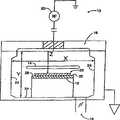
图1描述了可以在本发明中使用的平行板化学气相沉积反应器的剖视图。Figure 1 depicts a cross-sectional view of a parallel plate chemical vapor deposition reactor that can be used in the present invention.
图2描述了由本发明的超低k材料得到的傅立叶变换红外(“FTIR”)谱图,其中超低k材料由二乙氧基甲基硅烷(“DEMS”)和双环庚二烯(“BCHD”)的混合物沉积。Figure 2 depicts the Fourier Transform Infrared ("FTIR") spectrum obtained from an ultra-low-k material of the present invention composed of diethoxymethylsilane ("DEMS") and bicycloheptadiene ("BCHD"). ”) mixture deposition.
图3描述了由另一种本发明的超低k材料得到的傅立叶变换红外(“FTIR”)谱图,其中超低k材料由二乙氧基甲基硅烷(“DEMS”)和氧化环戊烯(“CPO”)的混合物沉积。Figure 3 depicts a Fourier transform infrared ("FTIR") spectrum obtained from another ultra-low-k material of the present invention, wherein the ultra-low-k material is composed of diethoxymethylsilane ("DEMS") and cyclopentyl oxide Deposition of a mixture of olefins ("CPO").
图4描述了具有根据本发明的超低k材料的层内电介质层和层间电介质层的电子器件的放大的剖视图。FIG. 4 depicts an enlarged cross-sectional view of an electronic device having an intralevel dielectric layer and an interlevel dielectric layer of an ultra-low-k material according to the present invention.
图5描述了具有在根据本发明的超低k材料膜上面的附加的扩散阻挡电介质盖层的图4的电子结构的放大的剖视图。5 depicts an enlarged cross-sectional view of the electronic structure of FIG. 4 with an additional diffusion-barrier dielectric capping layer on top of an ultra-low-k material film according to the present invention.
图6描述了具有附加RIE硬掩模/抛光停止电介质盖层和在根据本发明的抛光停止层上面的电介质盖扩散阻挡层的图5的电子结构的放大的剖视图。6 depicts an enlarged cross-sectional view of the electronic structure of FIG. 5 with an additional RIE hardmask/polish stop dielectric cap layer and a dielectric cap diffusion barrier layer on top of the polish stop layer according to the present invention.
图7描述了具有在根据本发明的层间超低k材料膜上面的附加的RIE硬掩模/抛光停止电介质层的图6的电子结构的放大的剖视图。7 depicts an enlarged cross-sectional view of the electronic structure of FIG. 6 with an additional RIE hardmask/polish stop dielectric layer on top of an interlayer ultra-low-k material film according to the present invention.
图8是具有沉积在多相材料膜上面的附加的RIE硬掩模/抛光停止电介质层的图7的电子结构的放大的剖视图。8 is an enlarged cross-sectional view of the electronic structure of FIG. 7 with an additional RIE hardmask/polish stop dielectric layer deposited on top of the multiphase material film.
具体实施方式Detailed ways
本发明公开了在平行板等离子体增强化学气相沉积(“PECVD”)反应器内制造热稳定的超低介电常数膜的方法。在优选的实施方案中公开的材料包含氢化氧化的硅碳材料(SiCOH)基质,其包括Si、C、O和H,处于无规共价键合的网状结构且介电常数不超过约2.5,其可以进一步包含分子尺寸的洞,直径约0.5-20纳米,进一步降低介电常数到低于约2.0的数值。更优选地,超低k膜的介电常数是从约1.5-约2.5,和最优选介电常数为从约1.8-约2.25。本发明的超低k电介质材料一般特征在于多相膜和多个纳米尺寸的孔,该多相膜包括基本由Si、C、O和H组成的第一相和基本由C和H组成的第二相。The present invention discloses a method for fabricating thermally stable ultra-low dielectric constant films in a parallel plate plasma enhanced chemical vapor deposition ("PECVD") reactor. In a preferred embodiment the disclosed materials comprise a hydrogenated oxidized silicon carbon material (SiCOH) matrix comprising Si, C, O and H in a random covalently bonded network and having a dielectric constant not exceeding about 2.5 , which may further comprise molecular-sized holes, about 0.5-20 nm in diameter, further reducing the dielectric constant to a value below about 2.0. More preferably, the ultra-low k film has a dielectric constant of from about 1.5 to about 2.5, and most preferably a dielectric constant of from about 1.8 to about 2.25. The ultra-low-k dielectric materials of the present invention are generally characterized by a multiphase film comprising a first phase consisting essentially of Si, C, O, and H and a second phase consisting essentially of C and H, and a plurality of nanometer-sized pores. two phase.
为了制造超低k热稳定膜,需要带有特定生长条件的特定几何形状的沉积反应器。例如,在平行板反应器内,基体卡盘的导电面积应介于约300cm2-约800cm2之间,基体和顶部电极之间的缝隙约1cm-约10cm。施加RF功率到基体上。根据本发明,由硅烷衍生物如DEMS和第二种前体的混合物在特定构型的沉积反应器内,在特定反应条件下形成超低k膜,其中第二种前体是有机分子,选自下列化合物,包括:To fabricate ultra-low-k thermally stable films, a deposition reactor of a specific geometry with specific growth conditions is required. For example, in a parallel plate reactor, the substrate chuck should have a conductive area between about 300 cm2 and about 800 cm2 , with a gap between the substrate and the top electrode of about 1 cm to about 10 cm. Apply RF power to the substrate. According to the present invention, an ultra-low-k film is formed from a mixture of silane derivatives such as DEMS and a second precursor in a deposition reactor with a specific configuration under specific reaction conditions, wherein the second precursor is an organic molecule, selected Compounds from the following, including:
烯烃:
炔烃:Alkynes:
醚:和ether: and
环氧烷烃:
其中R1、R2、R3、R4、R5和R6可以相同或不相同并选自氢、烷基、烯基或炔基,这些基团可以是线型的、支化的、环状的、多环的并可以用含氧、氮或氟的取代基团官能化,如双环庚二烯(BCHD)。本发明的超低k膜可以进一步在不低于约300℃的温度下进行热处理至少约0.25小时,以降低介电常数。此膜还可以在沉积后或在热处理之后进行UV或电子束处理。在此后沉积处理步骤过程中,由包括碳和氢和任选地氧原子的第二种前体气体(或气体混合物)得到的分子碎片会热分解并转变成更小的分子,这些小分子被从膜中释放掉。任选地,在膜中通过分子碎片的转变和释放过程,可以得到进一步形成的空洞。这样膜密度降低,介电常数和折光指数相应降低。wherein R1 , R2 , R3 , R4 , R5 and R6 may be the same or different and are selected from hydrogen, alkyl, alkenyl or alkynyl, and these groups may be linear, branched, Cyclic, polycyclic and can be functionalized with oxygen-, nitrogen- or fluorine-containing substituents, such as bicycloheptadiene (BCHD). The ultra-low-k film of the present invention may be further heat-treated at a temperature not lower than about 300° C. for at least about 0.25 hours to lower the dielectric constant. The film can also be UV or e-beam treated after deposition or after thermal treatment. During the subsequent deposition processing steps, the molecular fragments resulting from the second precursor gas (or gas mixture) comprising carbon and hydrogen and optionally oxygen atoms are thermally decomposed and converted into smaller molecules, which are released from the membrane. Optionally, further formation of cavities can be obtained in the membrane through transformation and release processes of molecular fragments. In this way, the film density is reduced, and the dielectric constant and refractive index are correspondingly reduced.
本发明提供制备具有超低k即低于约2.5的材料的方法,该材料适用于BEOL配线结构中的集成化。更优选地,本发明的超低k膜的介电常数为从约1.5-约2.5,和最优选地,介电常数为从约1.8-约2.25。可以通过至少两种合适前体的选择和如下所述的加工参数的特定的结合来制备本发明的膜。优选地,第一种前体选自具有分子式SiRR’R”R”’的硅烷(SiH4)衍生物,其中R、R’、R”和R”’可以相同或不同,且选自H、烷基和烷氧基,优选甲基、乙基、甲氧基和乙氧基。优选的前体包括:二乙氧基二甲基硅烷、二乙氧基甲基硅烷(DEMS)、乙氧基三甲基硅烷、乙氧基二甲基硅烷、二甲氧基二甲基硅烷、二甲氧基甲基硅烷、三乙氧基硅烷和三甲氧基甲基硅烷。The present invention provides methods for preparing materials with ultra-low k, ie below about 2.5, suitable for integration in BEOL wiring structures. More preferably, the ultralow-k films of the present invention have a dielectric constant of from about 1.5 to about 2.5, and most preferably, a dielectric constant of from about 1.8 to about 2.25. The membranes of the present invention can be prepared by the selection of at least two suitable precursors and a specific combination of processing parameters as described below. Preferably, the first precursor is selected from silane (SiH4 ) derivatives having the formula SiRR'R"R"', wherein R, R', R" and R"' may be the same or different, and are selected from H, Alkyl and alkoxy, preferably methyl, ethyl, methoxy and ethoxy. Preferred precursors include: diethoxydimethylsilane, diethoxymethylsilane (DEMS), ethoxytrimethylsilane, ethoxydimethylsilane, dimethoxydimethylsilane , Dimethoxymethylsilane, Triethoxysilane and Trimethoxymethylsilane.
在本申请中使用的第二种前体是选自下式的有机化合物:The second precursor used in this application is an organic compound selected from the following formulae:
烯烃:
炔烃:
醚:
环氧烷烃:
其中R1、R2、R3、R4、R5和R6可以相同或不同并选自氢、烷基、烯基或炔基,这些基团可以是线型的、支化的、环状的、多环的并可以用含氧、氮或氟的取代基团官能化。此外,在第二种前体分子中可以包含其它原子如S、Si或其它卤素。在这些物质中,最合适的是环氧乙烷、环氧丙烷、氧化环戊烯、氧化异丁烯、2,2,3-三甲基环氧乙烷、一氧化丁二烯、双环庚二烯、1,2-环氧基-5-己烯、2-甲基-2-乙烯基环氧乙烷、1-异丙基-环己-1,3-二烯和叔丁基甲基醚。wherein R1 , R2 , R3 , R4 , R5 and R6 can be the same or different and are selected from hydrogen, alkyl, alkenyl or alkynyl, and these groups can be linear, branched, cyclic Shaped, polycyclic and can be functionalized with oxygen, nitrogen or fluorine containing substituent groups. In addition, other atoms such as S, Si or other halogens may be included in the second precursor molecule. Among these substances, the most suitable are ethylene oxide, propylene oxide, cyclopentene oxide, isobutylene oxide, 2,2,3-trimethyloxirane, butadiene monoxide, dicycloheptadiene , 1,2-epoxy-5-hexene, 2-methyl-2-vinyloxirane, 1-isopropyl-cyclohexa-1,3-diene and tert-butyl methyl ether.
如图1所示,平行板等离子体增强化学气相沉积(“PECVD”)反应器10是用于加工200mm晶片使用的类型。反应器10的内径X大约为13英寸,而其高Y大约为8.5英寸。基体卡盘12的直径大约为10.8英寸。通过气体分配板(“GDP”)16将反应物气体引入到反应器10中,气体分配板被约1英寸的缝隙Z与基体卡盘12分隔开,和通过3英寸的排气口18将反应物气体排出反应器10。RF功率20与GDP16连接,GDP16与反应器10电绝缘,基体卡盘12接地。为了实用的目的,反应器的所有其它部件都接地。在不同的实施方案中,RF功率20可以与基体卡盘12连接并被传输到基体22上。在此情况下,基体要求负偏压,其值取决于反应器的几何形状和等离子体参数。在另一个实施方案中,可以使用多于一个的电源。例如,两个电源可以以相同的RF频率工作,或一个以低频工作而另一个以高频工作。两个电源可以都与相同的电极连接或被连接到单独的电极上。在另一个实施方案中,在沉积过程中可以启动或关闭RF电源。在低k膜的沉积过程中控制的工艺变量是RF功率密度、前体混合物和流速、反应器内压力、电极间距和基体温度(加热的晶片卡盘的温度控制基体温度)。As shown in FIG. 1, a parallel plate plasma enhanced chemical vapor deposition ("PECVD")
根据本发明,使用合适的第一种和第二种前体和上述工艺参数的特定结合,这样制备的本发明的超低k材料优选包括:约5-约40原子百分比的Si;约5-约70原子百分比的C;O-约50原子百分比的O;和约5-约55原子百分比的H。在本发明的一些实施方案中,C含量可以高达约70%。According to the present invention, using suitable first and second precursors and a specific combination of the above-mentioned process parameters, the ultra-low-k materials of the present invention thus prepared preferably include: about 5 to about 40 atomic percent Si; about 5 to about 40 atomic percent; about 70 atomic percent C; O to about 50 atomic percent O; and about 5 to about 55 atomic percent H. In some embodiments of the invention, the C content can be as high as about 70%.
在膜的沉积工艺过程中控制的主要工艺变量是RF功率、前体的流速、反应器压力和基体温度。在下文中提到的是根据本发明由第一种前体二乙氧基甲基硅烷(DEMS)和第二种前体双环庚二烯(BCHD)沉积膜的一些例子。在一些实施例中,通过使用He(或Ar)作为载气将DEMS前体蒸汽输送到反应器内。任选地,将膜在沉积后,在400℃下进行热处理以降低k。另外,例如,如在美国申请系列号10/758,724中所述,将膜进行UV或电子束处理以降低k和增加交联。热处理可以单独使用或与在‘724申请中公开的处理方法之一一起使用。The main process variables controlled during the film deposition process are RF power, flow rate of precursors, reactor pressure and substrate temperature. Mentioned below are some examples of films deposited according to the invention from a first precursor diethoxymethylsilane (DEMS) and a second precursor bicycloheptadiene (BCHD). In some embodiments, the DEMS precursor vapor is delivered into the reactor by using He (or Ar) as a carrier gas. Optionally, the film is heat treated at 400° C. after deposition to lower k. Additionally, films are subjected to UV or e-beam treatment to lower k and increase crosslinking, for example, as described in US Application Serial No. 10/758,724. Heat treatment may be used alone or with one of the treatments disclosed in the '724 application.
特定地,根据‘724申请,可以使用一种能量源任选地处理该沉积膜,以稳定此膜并提高其性能(电的、机械的、粘合的),生成最终优化的膜。合适的能量源包括热、化学、紫外线(UV)、电子束(e-束)、微波和等离子体。在本发明中也可以使用上述能量源的结合。利用在本发明中使用的能量源来改善该沉积的电介质的Si-O键合的网状结构,改善材料中的其它键,形成更多的Si-O交联,和在一些情况下去除烃相,其中所有上述改性均导致较高的弹性模量、较高的硬度或较低的内应力,或是上述性能的结合。无论较高的模量还是较低的应力均导致较低的裂纹扩展速度,而较高模量和较低应力的结合是能量处理的优选结果。Specifically, according to the '724 application, the deposited film can be optionally treated with an energy source to stabilize the film and improve its properties (electrical, mechanical, adhesive) resulting in a final optimized film. Suitable energy sources include thermal, chemical, ultraviolet (UV), electron beam (e-beam), microwave and plasma. Combinations of the above energy sources may also be used in the present invention. Utilize the energy source used in the present invention to improve the Si-O bonded network of the deposited dielectric, improve other bonds in the material, form more Si-O cross-links, and in some cases remove hydrocarbons phase, where all of the above modifications lead to higher elastic modulus, higher hardness, or lower internal stress, or a combination of the above properties. Both higher modulus and lower stress lead to lower crack growth rates, and the combination of higher modulus and lower stress is a preferred outcome of energy processing.
热能源包括任何来源例如加热元件或灯,其可以将沉积的电介质材料加热到约300℃-约500℃的温度。更优选地,热能源能够加热沉积的电介质材料到约350℃-约430℃的温度。此热处理工艺可以进行各种时间段,其中该时间段一般为约1分钟-约300分钟。此热处理步骤一般在惰性气体如He和Ar存在下进行。该热处理步骤可以被称作为退火步骤,其中使用快速热退火、炉内退火、激光退火或点火(spike)退火状态。Thermal energy sources include any source such as heating elements or lamps that can heat the deposited dielectric material to a temperature of about 300°C to about 500°C. More preferably, the thermal energy source is capable of heating the deposited dielectric material to a temperature of from about 350°C to about 430°C. This heat treatment process can be performed for various periods of time, wherein the period of time is generally from about 1 minute to about 300 minutes. This heat treatment step is generally performed in the presence of inert gases such as He and Ar. This heat treatment step may be referred to as an annealing step, where rapid thermal annealing, furnace annealing, laser annealing or spike annealing regimes are used.
使用能够产生波长为约500-约150nm的光的能量源进行UV光处理步骤,来照射基体,同时晶片温度保持在25℃-500℃,其中优选300℃-450℃的温度。>370nm的照射对于分裂或活化重要的键是不足的能量,因此波长范围150-370nm是优选的范围。利用文献资料和对沉积膜测量的吸收谱图,本发明者已经发现由于SiCOH膜的降解,<170nm的照射可能是不利的。进一步,由于310-370nm中每光子的相对低的能量,310-370nm的能量范围不如150-310nm范围有用。在150-310nm范围内,可以任选地使用该沉积膜的吸收谱图的最佳交叠和膜性能(如疏水性)的最小降解,以选择最有效的UV谱图区用于改变SiCOH的性能。The UV light treatment step is performed to irradiate the substrate using an energy source capable of producing light having a wavelength of about 500 to about 150 nm, while the wafer temperature is maintained at 25°C to 500°C, with a temperature of 300°C to 450°C being preferred. Irradiation at >370nm is insufficient energy to split or activate important bonds, so the wavelength range 150-370nm is the preferred range. Using literature data and absorption spectra measured on deposited films, the inventors have found that <170 nm irradiation may be disadvantageous due to degradation of SiCOH films. Further, the energy range of 310-370 nm is not as useful as the range of 150-310 nm due to the relatively low energy per photon in 310-370 nm. In the 150-310 nm range, optimal overlap of the absorption spectra of the deposited film and minimal degradation of film properties (such as hydrophobicity) can optionally be used to select the most effective UV spectral region for modifying the SiCOH performance.
使用能够在晶片上产生均匀的电子流量的能量源进行电子束处理步骤,其中能量为0.5-25keV和电流密度为0.1-100微安/cm2(优选1-5微安/cm2),同时晶片温度保持在25℃-500℃,优选300℃-450℃的温度。在电子束处理步骤中使用的优选的电子剂量为50-500微库仑/cm2,最优选100-300微库仑/cm2。The electron beam treatment step is carried out using an energy source capable of producing a uniform flux of electrons on the wafer with an energy of 0.5-25 keV and a current density of 0.1-100 microamperes/cm2 (preferably 1-5 microamperes/cm2 ), while The wafer temperature is maintained at a temperature ranging from 25°C to 500°C, preferably from 300°C to 450°C. The preferred electron dose used in the electron beam treatment step is 50-500 microcoulomb/cm2 , most preferably 100-300 microcoulomb/cm2 .
使用能够产生原子氢(H)和任选地CH3或其它烃基团的源进行等离子体处理步骤。优选下游等离子体源胜过直接等离子体照射。在等离子体处理过程中,晶片温度保持在25℃-500℃,优选300℃-450℃的温度。The plasma treatment step is performed using a source capable of generating atomic hydrogen (H) and optionallyCH3 or other hydrocarbon groups. A downstream plasma source is preferred over direct plasma irradiation. During the plasma treatment, the wafer temperature is maintained at a temperature of 25°C to 500°C, preferably 300°C to 450°C.
通过将气体引入到能产生等离子体的反应器内和之后气体转变成等离子体进行等离子体处理步骤。等离子体处理可以使用的气体包括惰性气体如Ar、N、He、Xe或Kr,其中优选He;氢或原子氢的相关来源、甲烷、甲基硅烷、CH3基团的相关来源及其混合物。等离子体处理气体的流速可以根据使用的反应器体系改变。室压可以在0.05-20torr范围内的任意点,但是工作压力的优选范围是1-10torr。等离子体处理步骤进行一段时间,尽管在本发明中可以使用较长的时间,但其一般为约1/2-约10分钟。The plasma treatment step is performed by introducing a gas into a reactor capable of generating a plasma and thereafter converting the gas into a plasma. Gases that can be used for plasma treatment include noble gases such as Ar, N, He, Xe or Kr, with He being preferred; hydrogen or related sources of atomic hydrogen, methane, methylsilane, related sources ofCH3 groups and mixtures thereof. The flow rate of the plasma treatment gas can vary depending on the reactor system used. The chamber pressure can be anywhere within the range of 0.05-20 torr, but the preferred range of working pressure is 1-10 torr. The plasma treatment step is performed for a period of time, generally from about 1/2 to about 10 minutes, although longer times can be used in the present invention.
一般使用RF或微波功率源产生上述等离子体。RF功率源可以在高频范围(在约100W或更高的数量级)或低频范围(低于250W)内工作或者可以使用它们的结合。高频功率密度可以在0.1-2.0W/cm2范围内任意点,但是优选的工作范围是0.2-1.0W/cm2。低频功率密度可以在0.1-1.0W/cm2范围内任意点,但是优选的工作范围是0.2-0.5W/cm2。选择的功率水平必须足够低,以避免曝光的电介质表面显著的溅射蚀刻(<5纳米去除)。Such plasmas are typically generated using RF or microwave power sources. The RF power source may operate in the high frequency range (on the order of about 100W or higher) or low frequency range (below 250W) or a combination thereof may be used. The high frequency power density can be anywhere within the range of 0.1-2.0 W/cm2 , but the preferred working range is 0.2-1.0 W/cm2 . The low frequency power density can be anywhere within the range of 0.1-1.0 W/cm2 , but the preferred working range is 0.2-0.5 W/cm2 . The selected power level must be low enough to avoid significant sputter etching (<5 nm removal) of the exposed dielectric surface.
使用的沉积条件也很严格,以能够成功的进行根据本发明的沉积工艺。例如,使用约25℃-约420℃之间,和优选60℃-约350℃之间的晶片温度。使用约0.05W/cm2-约3.5W/cm2之间,和优选约0.25W/cm2-约1W/cm2之间的RF功率密度。在优选的工艺中,不仅将照射频率能量以13.6MHz和约350W的功率(尽管可以使用200-450W)施加到气体引入板(“淋浴头”),而且将其以13.6MHz和约100W的功率(尽管可以使用50-200W)施加到晶片卡盘上。如现有技术中已知,在本发明中也可以使用不同的RF频率(0.26、0.35、0.45MHz)。The deposition conditions used are also severe in order to be able to successfully carry out the deposition process according to the present invention. For example, wafer temperatures between about 25°C and about 420°C, and preferably between 60°C and about 350°C, are used. RF power densities between about 0.05 W/cm2 and about 3.5 W/cm2 , and preferably between about 0.25 W/cm2 and about 1 W/cm2 are used. In a preferred process, irradiation frequency energy is applied not only to the gas introduction plate ("shower head") at 13.6 MHz and about 350 W (although 200-450 W can be used), but also at 13.6 MHz and about 100 W 50-200W) can be used to apply to the wafer chuck. Different RF frequencies (0.26, 0.35, 0.45 MHz) may also be used in the present invention as known in the art.
使用约5sccm-约1000sccm之间,和优选地约25sccm-约200sccm之间的DEMS反应物气体流速。使用约5sccm-约1000sccm之间,和优选地约10sccm-约120sccm之间的BCHD的反应物气体流速。当使用液体前体释放输送时,每种前体使用500-5000mg/分钟的液体流速。任选地,可以加入He和优选的He的流速在100-2000sccm范围内,尽管在本发明中可以使用其它流体。沉积过程中反应器压力一般在约50mtorr-约10000mtorr之间。DEMS reactant gas flow rates between about 5 seem and about 1000 seem, and preferably between about 25 seem and about 200 seem, are used. A reactant gas flow rate for BCHD of between about 5 seem to about 1000 seem, and preferably between about 10 seem to about 120 seem is used. When using liquid precursor release delivery, a liquid flow rate of 500-5000 mg/min of each precursor was used. Optionally, He may be added and preferably He flow rates are in the range of 100-2000 seem, although other fluids may be used in the present invention. Reactor pressure during deposition is typically between about 50 mtorr and about 10,000 mtorr.
如果使用多站沉积反应器,基体的面积参照每一个单个基体卡盘和气体流速参照每一个单个沉积站。因此,到反应器的总流速和总的功率输入被反应器内沉积站点的总数相乘。If a multi-station deposition reactor is used, the area of the substrate is referenced to each individual substrate chuck and the gas flow rate is referenced to each individual deposition station. Thus, the total flow rate and total power input to the reactor is multiplied by the total number of deposition stations within the reactor.
在进行进一步的集成加工之前,沉积膜是稳定的。稳定化工艺可以在炉内退火步骤中约300℃-约430℃下进行约0.5小时-约4小时。稳定化工艺也可以在快速热退火步骤中在超过300℃的温度下进行。稳定化工艺还可以在UV或电子束室内在超过300℃的温度下进行。根据本发明得到的膜的介电常数低于约2.5。在非氧化环境中,根据本发明得到的膜的热稳定性高达至少约430℃的温度。The deposited film is stable until further integration processing. The stabilization process may be performed at about 300° C. to about 430° C. for about 0.5 hours to about 4 hours in the furnace annealing step. The stabilization process can also be performed at temperatures in excess of 300°C in a rapid thermal annealing step. The stabilization process can also be performed in a UV or electron beam chamber at temperatures in excess of 300°C. Films obtained according to the present invention have dielectric constants below about 2.5. In a non-oxidizing environment, the thermal stability of the films obtained according to the present invention is up to a temperature of at least about 430°C.
根据本发明形成的电子器件示于图4-7。应当指出:图4-7中所示的器件仅作为根据本发明的例子说明,而根据本发明也可以形成无数其它的器件。Electronic devices formed in accordance with the present invention are shown in Figures 4-7. It should be noted that the devices shown in Figs. 4-7 are only illustrated as examples in accordance with the present invention, and that countless other devices can also be formed in accordance with the present invention.
图4描述了建在硅基体32上的电子器件30。在硅基体32的顶部形成绝缘材料层34,其中嵌入第一个金属区36。在第一个金属区36上进行化学机械抛光(“CMP”)工艺后,诸如超低k膜38的一层膜就沉积在了第一层绝缘材料34和第一个金属区36的上面。任选地,可以在层34和层38之间加入一层附加的电介质盖层(未示意出)。第一层绝缘材料34可以由氧化硅、氮化硅、这些材料的多种掺杂体,或者任何其它合适的绝缘材料恰当地形成。超低k膜38由光刻蚀工艺形成图案和导体层40沉积在其中。在第一个导体层40上进行CMP工艺之后,由等离子体增强化学气相沉积(“PECVD”)工艺在第一个超低k膜38和第一个导体层40上面沉积第二层超低k膜44。导体层40可以由金属导电材料或非金属导电材料沉积而成。例如,可以使用铝或铜的金属导电材料,或如氮化物或聚硅的非金属材料。第一个导体40与第一个金属区36电连通。FIG. 4 depicts an electronic device 30 built on a
在第二个超低k膜层44内进行光刻蚀工艺之后,形成第二个导体区50,随后进行第二个导体材料的沉积工艺。第二个导体50也可以由金属材料或非金属材料沉积而成,与沉积第一个导体层40中使用的材料相似。第二个导体区50与第一个导体区40电连通并嵌入在第二层超低k绝缘体44中。第二层超低k膜与第一层绝缘材料38紧密接触。在此特定的实施例中,是根据本发明的超低k材料的第一层绝缘材料38用作层内电介质材料,而第二层绝缘材料即超低k膜44既用作层内又用作层间电介质。以超低k膜的低的介电常数为基础,可以由第一个绝缘层38和第二个绝缘层44获得超级绝缘性能。After the photoetching process is performed in the second ultra-low-
图5描述了根据本发明的电子器件60,与图4中示意的电子器件30相似,但是具有沉积在第一个绝缘材料层38和第二个绝缘材料层44之间的附加电介质盖层62。电介质盖层62可以由诸如氧化硅、氮化硅、氧氮化硅、碳化硅、碳氮化硅(SiCN)、碳氧化硅(SiCO)、改性的超低k及其氢化化合物以及难熔金属氮化硅等材料恰当地形成,其中难熔金属选自:Ta、Zr、Hf和W。此外,电介质盖层62用作扩散阻挡层以阻止第一个导体层40扩散进入第二个绝缘材料层44中或进入下面的层,尤其是层34和32中。FIG. 5 depicts an
图6描述了根据本发明的电子器件70的另一个替代的实施方案。在电子器件70中,使用两个用作RIE掩模和CMP(化学-机械抛光)抛光停止层的附加的电介质盖层72和74。第一个电介质盖层72沉积在第一个绝缘材料层38上面。电介质层72的功能是提供一个在平面化第一个导体层40中使用的CMP工艺的端点。抛光停止层72可以由合适的电介质材料如氧化硅、氮化硅、氧氮化硅、碳化硅、碳氧化硅(SiCO)、碳氮化硅(SiCN)改性的超低k及其氢化化合物以及难熔金属氮化硅沉积形成,其中难熔金属选自:Ta、Zr、Hf和W。电介质层72的上表面与第一个导体层40处于同一水平面。第二个电介质层74可以加在第二个绝缘材料层44的上面用于相同的目的。FIG. 6 depicts another alternative embodiment of an
图7又描述了根据本发明的电子器件80的另一个替代的实施方案。在此替代实施方案中,沉积了附加的电介质层82,这样将第二个绝缘材料层44分成了两个单独的层84和86。因此,如图7所述,层内和层间电介质层44在互连体92和互连体94间的界面处被分成层内电介质层84和层间电介质层86,如图8所述。附加的扩散阻挡层96被进一步沉积在上部的电介质层74的上面。由此电子结构80的替代的实施方案提供的额外的好处是电介质层82作为RIE蚀刻停止,提供优良的互连深度控制,和因此对导体电阻的优良控制。FIG. 7 depicts yet another alternative embodiment of an
举出下列实施例来说明根据本发明的超低k电介质膜的制造并证明由此得到的膜的优点:The following examples are presented to illustrate the fabrication of ultra-low-k dielectric films according to the invention and to demonstrate the advantages of the films thus obtained:
实施例1Example 1
在此实施例中,根据图1,首先通过槽阀(slit valve)14将晶片引入到反应器10内制备晶片和将晶片任选地由氩气进行预蚀刻。在此晶片制备工艺中,晶片温度设定在约180℃和氩气流速设定为约25sccm,以获得约100mtorr的压力。然后接通约125W的RF功率持续约60秒。然后关掉RF功率和氩气流。In this example, according to FIG. 1 , the wafer is first prepared by introducing the wafer into the
加入DEMS前体到反应器内。通过首先将DEMS和BCHD的气流固定在预期的流速和压力,即约4sccm的DEMS和约3sccm的BCHD和约500mtorr,沉积根据本发明的超低K膜。然后接通约30W的RF功率持续约50分钟。再关掉RF功率和气流。然后从反应器10中移出该晶片。Add the DEMS precursor to the reactor. Ultra-low K films according to the present invention were deposited by first fixing the gas streams of DEMS and BCHD at the desired flow rates and pressures, ie about 4 seem for DEMS and about 3 seem for BCHD and about 500 mtorr. RF power of about 30W was then turned on for about 50 minutes. Then turn off the RF power and air flow. The wafer is then removed from the
为了降低该沉积膜的介电常数和进一步提高它们的热稳定性,即:使它们在大于300℃的温度下稳定,将此膜进行后处理,以蒸发易挥发的成分并在尺寸上稳定该膜。后处理工艺可以由下列步骤在退火炉内进行。首先将炉用氮气以约10升/分钟的流速清洗约5分钟(其中膜样品在负载站内)。然后将膜样品转移到炉反应器内,开始如下后退火循环:以约5℃/分钟的加热速度加热该膜到约280℃,在约280℃下保持约5分钟,以约5℃/分钟的加热速度第二次加热到约400℃,在约400℃下保持约4小时,关掉炉子并使膜样品冷却到低于约100℃的温度。合适的第一个保持温度可以在约280℃-约300℃之间,而合适的第二个保持温度可以在约300℃-约400℃之间。这样得到的膜的介电常数为1.81。此外,该膜可以在超过300℃下进行UV或电子束处理达30分钟。In order to lower the dielectric constant of the deposited films and further increase their thermal stability, i.e. to stabilize them at temperatures greater than 300°C, the films are post-treated to evaporate volatile components and dimensionally stabilize the membrane. The post-treatment process can be carried out in the annealing furnace by the following steps. The furnace was first purged with nitrogen for about 5 minutes at a flow rate of about 10 liters/minute (with the membrane sample in the loading station). The film sample was then transferred into a furnace reactor and a post-annealing cycle was initiated as follows: heat the film to about 280°C at a heating rate of about 5°C/min, hold at about 280°C for about 5 minutes, heat at about 5°C/min The heating rate is a second heat to about 400°C, hold at about 400°C for about 4 hours, turn off the furnace and allow the film sample to cool to a temperature below about 100°C. A suitable first hold temperature may be between about 280°C and about 300°C, and a suitable second hold temperature may be between about 300°C and about 400°C. The dielectric constant of the film thus obtained was 1.81. In addition, the film can be UV or e-beam treated at over 300°C for 30 minutes.
现在参见图2讨论第一个实施方案的结果。图2代表由根据本发明的DEMS+BCHD的混合物制备的超低k膜得到的FTIR谱图。该谱图显示出在约1000-1100cmm-1处Si-O吸收段、在约1268cm-1处Si-CH3吸收峰和在约2900-3000cm-1处C-H吸收峰。该超低k膜的此FTIR谱图的一个特征是Si-O峰可以被解卷积为中心在1141cm-1、1064cmm-1和1030cm-1处的3个峰,如图2中特别示意。Referring now to Figure 2, the results of the first embodiment are discussed. Figure 2 represents the FTIR spectrum obtained from an ultra-low-k film prepared from a mixture of DEMS+BCHD according to the invention. The spectrum shows a Si-O absorption segment at about 1000-1100 cm-1 , a Si-CH absorption peak at about 1268 cm-1and a CH absorption peak at about 2900-3000 cm- 1. A feature of this FTIR spectrum of the ultra-low-k film is that the Si—O peak can be deconvoluted into 3 peaks centered at 1141 cm−1 , 1064 cm−1 and 1030 cm−1 , as specifically illustrated in FIG. 2 .
实施例2Example 2
在此实施例中,在如实施例1相同的设备中制备晶片。首先将晶片引入到反应室内。晶片温度设定在约180℃。将DEMS前体装入反应器内。通过首先将DEMS和一氧化丁二烯(BMO)的气流固定在预期的流速和压力,即约1sccm的DEMS和约4sccm的BMO和约500mtorr下,沉积根据本发明的超低K膜。然后接通约30W的RF功率持续约50分钟。再关掉RF功率和气流。然后从反应器10中移出晶片。In this example, wafers were prepared in the same apparatus as in Example 1. First the wafer is introduced into the reaction chamber. The wafer temperature was set at about 180°C. The DEMS precursor was loaded into the reactor. Ultra-low K films according to the present invention were deposited by first fixing the gas streams of DEMS and butadiene monoxide (BMO) at the desired flow rates and pressures, namely about 1 sccm of DEMS and about 4 sccm of BMO and about 500 mtorr. RF power of about 30W was then turned on for about 50 minutes. Then turn off the RF power and air flow. The wafer is then removed from the
然后将此膜以实施例1中所述的相同方法进行处理。得到的膜的介电常数为1.77。This film was then treated in the same manner as described in Example 1. The resulting film had a dielectric constant of 1.77.
实施例3Example 3
在此实施例中,在如实施例1相同的设备中制备晶片。首先将晶片引入到反应室内。晶片温度设定在约180℃。将DEMS前体装入反应器内。通过首先将DEMS和2-甲基-2-乙烯基环氧乙烷(MVOX)的气流固定在预期的流速和压力,即约2sccm的DEMS和约3sccm的MVOX和约500mtorr下,沉积根据本发明的超低K膜。然后接通约30W的RF功率持续约50分钟。再关掉RF功率和气流。然后从反应器10中移出晶片。In this example, wafers were prepared in the same apparatus as in Example 1. First the wafer is introduced into the reaction chamber. The wafer temperature was set at about 180°C. The DEMS precursor was loaded into the reactor. Deposit the supernatant according to the present invention by first fixing the gas flow of DEMS and 2-methyl-2-vinyloxirane (MVOX) at the desired flow rate and pressure, namely about 2 sccm of DEMS and about 3 sccm of MVOX and about 500 mtorr. Low K film. RF power of about 30W was then turned on for about 50 minutes. Then turn off the RF power and air flow. The wafer is then removed from the
然后将此膜以实施例1中所述的相同方法进行处理。This film was then treated in the same manner as described in Example 1.
得到的膜的介电常数为2.08。The resulting film had a dielectric constant of 2.08.
实施例4Example 4
在此实施例中,在一个8英寸的工业PECVD设备中制备晶片。首先将晶片引入到反应室内。晶片温度设定在约200℃。使用He作为载气将DEMS和氧化环戊烯(CPO)都装入反应器内。通过首先将DEMS和CPO的气流和He固定在预期的流速和压力,即约70sccm的DEMS和约320sccm的CPO和约300sccm的He和约2000mtorr下,沉积根据本发明的超低K膜。然后接通约300W的RF功率持续约10分钟。再关掉RF功率和气流。然后从反应室中移出晶片。In this example, wafers were prepared in an 8-inch industrial PECVD tool. First the wafer is introduced into the reaction chamber. The wafer temperature was set at about 200°C. Both DEMS and cyclopentene oxide (CPO) were loaded into the reactor using He as the carrier gas. Ultra-low K films according to the present invention were deposited by first fixing the gas streams of DEMS and CPO and He at the desired flow rates and pressures, namely about 70 sccm of DEMS and about 320 sccm of CPO and about 300 sccm of He and about 2000 mtorr. RF power of about 300W was then turned on for about 10 minutes. Then turn off the RF power and air flow. The wafer is then removed from the reaction chamber.
然后将此膜以实施例1中所述的相同方法进行处理。得到的膜的介电常数为2.19。This film was then treated in the same manner as described in Example 1. The resulting film had a dielectric constant of 2.19.
现在参见图3讨论结果。图3代表得自于由DEMS/CPO和He制备的超低k膜的FTIR谱图。该谱图显示出在约1000-1100cm-1处Si-O吸收段、在约1267cm-1处Si-CH3吸收峰和在约2900-3000cm-1处C-H吸收峰。该超低k膜的FTIR谱图的一个特征是Si-O峰可以被解卷积为中心在1132cm-1、1058cm-1和1024cm-1处的3个峰,如图3中特别示意。Referring now to Figure 3 the results are discussed. Figure 3 represents the FTIR spectra obtained from ultra-low-k films prepared from DEMS/CPO and He. The spectrum shows a Si-O absorption segment at about 1000-1100 cm-1 , a Si-CH absorption peak at about 1267 cm-1and a CH absorption peak at about 2900-3000 cm- 1. A feature of the FTIR spectrum of this ultra-low-k film is that the Si—O peak can be deconvoluted into 3 peaks centered at 1132 cm−1 , 1058 cm−1 and 1024 cm−1 , as specifically illustrated in FIG. 3 .
也可以使用快速热退火(“RTA”)工艺来稳定超低k膜。根据本发明得到的膜的特征在于介电常数k小于约2.5,和它们对于在线后端(“BEOL”)互连结构中的集成化是热稳定的,该互连结构通常在达到约400℃的温度下进行加工。因此,本发明的教导可以很容易地适用于生产在线后端工艺中用作层内和层间电介质的膜,用于逻辑和记忆元件。A rapid thermal annealing ("RTA") process can also be used to stabilize ultra-low-k films. Films obtained in accordance with the present invention are characterized by a dielectric constant k of less than about 2.5, and that they are thermally stable for integration in back-end-of-line ("BEOL") interconnect structures, typically at temperatures up to about 400°C. processed at a temperature. Thus, the teachings of the present invention can be readily adapted to produce films used as intralayer and interlayer dielectrics in back-end-of-line processes for logic and memory components.
因此,在上述描述和附图4-8中已经完全证明了根据本发明的方法和形成的电子结构。应当强调:图4-8中所示的电子结构的例子仅是用于说明本发明的方法,其可以适用于无数电子器件的制造。Thus, the method and the electronic structures formed according to the invention have been fully demonstrated in the above description and in the accompanying drawings 4-8. It should be emphasized that the examples of electronic structures shown in Figures 4-8 are provided only to illustrate the method of the present invention, which can be applied to the fabrication of countless electronic devices.
正如现有技术已知,当使用液体质量流动控制时,在上面4个工艺实施例中列出的气流单元可以由液体流单元代替。As is known in the art, when liquid mass flow control is used, the gas flow units listed in the four process examples above can be replaced by liquid flow units.
尽管已经以说明的方式描述了本发明,但是应当理解使用的术语意图是描述性用词而非限制性。While the present invention has been described by way of illustration, it is to be understood that the terminology which has been used is intended to be words of description rather than limitation.
而且,尽管已经就优选的实施方案和几个替代的实施方案特别示意并说明了本发明,但是应当理解熟练的技术人员可以轻易地将这些教导应用于本发明的其它可能的变体,而不背离本发明的精神和范围。Moreover, while the invention has been particularly shown and described with respect to a preferred embodiment and several alternative embodiments, it should be understood that a skilled artisan can readily apply these teachings to other possible variations of the invention without depart from the spirit and scope of the invention.
在下面附带的权利要求书中定义了本发明的实施方案,其中要求了专有性质或特权。Embodiments of the present invention are defined in the following appended claims, where exclusive properties or privileges are claimed.
Claims (62)


Applications Claiming Priority (2)
| Application Number | Priority Date | Filing Date | Title |
|---|---|---|---|
| US10/838,849 | 2004-05-03 | ||
| US10/838,849US7049247B2 (en) | 2004-05-03 | 2004-05-03 | Method for fabricating an ultralow dielectric constant material as an intralevel or interlevel dielectric in a semiconductor device and electronic device made |
Publications (2)
| Publication Number | Publication Date |
|---|---|
| CN1950932A CN1950932A (en) | 2007-04-18 |
| CN100524648Ctrue CN100524648C (en) | 2009-08-05 |
Family
ID=34963531
Family Applications (1)
| Application Number | Title | Priority Date | Filing Date |
|---|---|---|---|
| CNB2005800116280AExpired - Fee RelatedCN100524648C (en) | 2004-05-03 | 2005-03-23 | Improved method for fabricating ultra-low dielectric constant materials for use as intralevel or interlevel dielectrics in fabricated semiconductor and electronic devices |
Country Status (7)
| Country | Link |
|---|---|
| US (2) | US7049247B2 (en) |
| EP (1) | EP1745504A1 (en) |
| JP (1) | JP4756036B2 (en) |
| KR (1) | KR100956580B1 (en) |
| CN (1) | CN100524648C (en) |
| TW (2) | TWI353637B (en) |
| WO (1) | WO2005112095A1 (en) |
Families Citing this family (440)
| Publication number | Priority date | Publication date | Assignee | Title |
|---|---|---|---|---|
| US7384471B2 (en)* | 2002-04-17 | 2008-06-10 | Air Products And Chemicals, Inc. | Porogens, porogenated precursors and methods for using the same to provide porous organosilica glass films with low dielectric constants |
| US8293001B2 (en)* | 2002-04-17 | 2012-10-23 | Air Products And Chemicals, Inc. | Porogens, porogenated precursors and methods for using the same to provide porous organosilica glass films with low dielectric constants |
| US9061317B2 (en) | 2002-04-17 | 2015-06-23 | Air Products And Chemicals, Inc. | Porogens, porogenated precursors and methods for using the same to provide porous organosilica glass films with low dielectric constants |
| US20080268177A1 (en)* | 2002-05-17 | 2008-10-30 | Air Products And Chemicals, Inc. | Porogens, Porogenated Precursors and Methods for Using the Same to Provide Porous Organosilica Glass Films with Low Dielectric Constants |
| US8951342B2 (en) | 2002-04-17 | 2015-02-10 | Air Products And Chemicals, Inc. | Methods for using porogens for low k porous organosilica glass films |
| US6936551B2 (en)* | 2002-05-08 | 2005-08-30 | Applied Materials Inc. | Methods and apparatus for E-beam treatment used to fabricate integrated circuit devices |
| US7060330B2 (en)* | 2002-05-08 | 2006-06-13 | Applied Materials, Inc. | Method for forming ultra low k films using electron beam |
| US7485570B2 (en) | 2002-10-30 | 2009-02-03 | Fujitsu Limited | Silicon oxycarbide, growth method of silicon oxycarbide layer, semiconductor device and manufacture method for semiconductor device |
| JP4338495B2 (en)* | 2002-10-30 | 2009-10-07 | 富士通マイクロエレクトロニクス株式会社 | Silicon oxycarbide, semiconductor device, and method of manufacturing semiconductor device |
| US7049247B2 (en)* | 2004-05-03 | 2006-05-23 | International Business Machines Corporation | Method for fabricating an ultralow dielectric constant material as an intralevel or interlevel dielectric in a semiconductor device and electronic device made |
| US7256124B2 (en)* | 2005-03-30 | 2007-08-14 | Taiwan Semiconductor Manufacturing Co., Ltd. | Method of fabricating semiconductor device |
| US7638859B2 (en)* | 2005-06-06 | 2009-12-29 | Taiwan Semiconductor Manufacturing Co., Ltd. | Interconnects with harmonized stress and methods for fabricating the same |
| JP2007214403A (en)* | 2006-02-10 | 2007-08-23 | Renesas Technology Corp | Method for manufacturing semiconductor device |
| FR2904728B1 (en) | 2006-08-01 | 2008-11-21 | Air Liquide | NOVEL POROGENOUS PRECURSORS AND POROUS DIELECTRIC LAYERS OBTAINED THEREFROM |
| US8053375B1 (en)* | 2006-11-03 | 2011-11-08 | Advanced Technology Materials, Inc. | Super-dry reagent compositions for formation of ultra low k films |
| US7749894B2 (en)* | 2006-11-09 | 2010-07-06 | Chartered Semiconductor Manufacturing Ltd. | Integrated circuit processing system |
| US7638443B2 (en)* | 2006-11-14 | 2009-12-29 | Asm Japan K.K. | Method of forming ultra-thin SiN film by plasma CVD |
| US7749892B2 (en)* | 2006-11-29 | 2010-07-06 | International Business Machines Corporation | Embedded nano UV blocking and diffusion barrier for improved reliability of copper/ultra low K interlevel dielectric electronic devices |
| JP5118337B2 (en)* | 2006-11-30 | 2013-01-16 | アペックス株式会社 | Excimer vacuum ultraviolet light irradiation treatment equipment |
| US20080173985A1 (en)* | 2007-01-24 | 2008-07-24 | International Business Machines Corporation | Dielectric cap having material with optical band gap to substantially block uv radiation during curing treatment, and related methods |
| US20080230907A1 (en)* | 2007-03-22 | 2008-09-25 | Chartered Semiconductor Manufacturing Ltd. | Integrated circuit system with carbon enhancement |
| US7615484B2 (en)* | 2007-04-24 | 2009-11-10 | Chartered Semiconductor Manufacturing Ltd. | Integrated circuit manufacturing method using hard mask |
| US20090061649A1 (en) | 2007-08-28 | 2009-03-05 | International Business Machines Corporation | LOW k POROUS SiCOH DIELECTRIC AND INTEGRATION WITH POST FILM FORMATION TREATMENT |
| US20090061237A1 (en)* | 2007-08-28 | 2009-03-05 | International Business Machines Corporation | LOW k POROUS SiCOH DIELECTRIC AND INTEGRATION WITH POST FILM FORMATION TREATMENT |
| US8378694B2 (en)* | 2007-10-05 | 2013-02-19 | 3M Innovative Properties Company | Organic chemical sensor comprising plasma-deposited microporous layer, and method of making and using |
| US8258629B2 (en)* | 2008-04-02 | 2012-09-04 | Taiwan Semiconductor Manufacturing Company, Ltd. | Curing low-k dielectrics for improving mechanical strength |
| US20100143580A1 (en)* | 2008-05-28 | 2010-06-10 | American Air Liquide, Inc. | Stabilization of Bicycloheptadiene |
| US8298965B2 (en)* | 2008-09-03 | 2012-10-30 | American Air Liquide, Inc. | Volatile precursors for deposition of C-linked SiCOH dielectrics |
| US10378106B2 (en) | 2008-11-14 | 2019-08-13 | Asm Ip Holding B.V. | Method of forming insulation film by modified PEALD |
| US20100151206A1 (en) | 2008-12-11 | 2010-06-17 | Air Products And Chemicals, Inc. | Method for Removal of Carbon From An Organosilicate Material |
| JP2010192520A (en) | 2009-02-16 | 2010-09-02 | Elpida Memory Inc | Method for manufacturing semiconductor device |
| SG174296A1 (en) | 2009-03-10 | 2011-10-28 | Air Liquide | Cyclic amino compounds for low-k silylation |
| US9394608B2 (en) | 2009-04-06 | 2016-07-19 | Asm America, Inc. | Semiconductor processing reactor and components thereof |
| US8802201B2 (en) | 2009-08-14 | 2014-08-12 | Asm America, Inc. | Systems and methods for thin-film deposition of metal oxides using excited nitrogen-oxygen species |
| EP2319821A1 (en) | 2009-11-06 | 2011-05-11 | L'Air Liquide Société Anonyme pour l'Etude et l'Exploitation des Procédés Georges Claude | Stabilization of bicycloheptadiene |
| US8314005B2 (en) | 2010-01-27 | 2012-11-20 | International Business Machines Corporation | Homogeneous porous low dielectric constant materials |
| US8492239B2 (en) | 2010-01-27 | 2013-07-23 | International Business Machines Corporation | Homogeneous porous low dielectric constant materials |
| WO2011103282A2 (en) | 2010-02-17 | 2011-08-25 | L'air Liquide, Societe Anonyme Pour L'etude Et L'exploitation Des Procedes Georges Claude | VAPOR DEPOSITION METHODS OF SiCOH LOW-K FILMS |
| CN102543844B (en)* | 2010-12-30 | 2014-05-14 | 中芯国际集成电路制造(上海)有限公司 | Method for manufacturing semiconductor device structure and semiconductor device structure |
| JP2012201658A (en)* | 2011-03-28 | 2012-10-22 | Tosoh Corp | Film-forming material, method of producing film using the same, and application thereof |
| CN102751233B (en)* | 2011-04-18 | 2015-03-11 | 中芯国际集成电路制造(上海)有限公司 | Interconnection structure forming method |
| US9312155B2 (en) | 2011-06-06 | 2016-04-12 | Asm Japan K.K. | High-throughput semiconductor-processing apparatus equipped with multiple dual-chamber modules |
| US9793148B2 (en) | 2011-06-22 | 2017-10-17 | Asm Japan K.K. | Method for positioning wafers in multiple wafer transport |
| US10364496B2 (en) | 2011-06-27 | 2019-07-30 | Asm Ip Holding B.V. | Dual section module having shared and unshared mass flow controllers |
| US8927430B2 (en) | 2011-07-12 | 2015-01-06 | International Business Machines Corporation | Overburden removal for pore fill integration approach |
| US8541301B2 (en) | 2011-07-12 | 2013-09-24 | International Business Machines Corporation | Reduction of pore fill material dewetting |
| US10854498B2 (en) | 2011-07-15 | 2020-12-01 | Asm Ip Holding B.V. | Wafer-supporting device and method for producing same |
| US20130023129A1 (en) | 2011-07-20 | 2013-01-24 | Asm America, Inc. | Pressure transmitter for a semiconductor processing environment |
| US8551892B2 (en) | 2011-07-27 | 2013-10-08 | Asm Japan K.K. | Method for reducing dielectric constant of film using direct plasma of hydrogen |
| US8828489B2 (en) | 2011-08-19 | 2014-09-09 | International Business Machines Corporation | Homogeneous modification of porous films |
| US9017481B1 (en) | 2011-10-28 | 2015-04-28 | Asm America, Inc. | Process feed management for semiconductor substrate processing |
| US8946830B2 (en) | 2012-04-04 | 2015-02-03 | Asm Ip Holdings B.V. | Metal oxide protective layer for a semiconductor device |
| TWI581331B (en)* | 2012-07-13 | 2017-05-01 | 應用材料股份有限公司 | Method to reduce dielectric constant of a porous low-k film |
| US9558931B2 (en) | 2012-07-27 | 2017-01-31 | Asm Ip Holding B.V. | System and method for gas-phase sulfur passivation of a semiconductor surface |
| US9659799B2 (en) | 2012-08-28 | 2017-05-23 | Asm Ip Holding B.V. | Systems and methods for dynamic semiconductor process scheduling |
| US9021985B2 (en) | 2012-09-12 | 2015-05-05 | Asm Ip Holdings B.V. | Process gas management for an inductively-coupled plasma deposition reactor |
| US9324811B2 (en) | 2012-09-26 | 2016-04-26 | Asm Ip Holding B.V. | Structures and devices including a tensile-stressed silicon arsenic layer and methods of forming same |
| US10714315B2 (en) | 2012-10-12 | 2020-07-14 | Asm Ip Holdings B.V. | Semiconductor reaction chamber showerhead |
| US9640416B2 (en) | 2012-12-26 | 2017-05-02 | Asm Ip Holding B.V. | Single-and dual-chamber module-attachable wafer-handling chamber |
| US20160376700A1 (en) | 2013-02-01 | 2016-12-29 | Asm Ip Holding B.V. | System for treatment of deposition reactor |
| US9589770B2 (en) | 2013-03-08 | 2017-03-07 | Asm Ip Holding B.V. | Method and systems for in-situ formation of intermediate reactive species |
| US9484191B2 (en) | 2013-03-08 | 2016-11-01 | Asm Ip Holding B.V. | Pulsed remote plasma method and system |
| US9058983B2 (en) | 2013-06-17 | 2015-06-16 | International Business Machines Corporation | In-situ hardmask generation |
| US8993054B2 (en) | 2013-07-12 | 2015-03-31 | Asm Ip Holding B.V. | Method and system to reduce outgassing in a reaction chamber |
| US9018111B2 (en) | 2013-07-22 | 2015-04-28 | Asm Ip Holding B.V. | Semiconductor reaction chamber with plasma capabilities |
| US9793115B2 (en) | 2013-08-14 | 2017-10-17 | Asm Ip Holding B.V. | Structures and devices including germanium-tin films and methods of forming same |
| TWI612182B (en)* | 2013-09-09 | 2018-01-21 | 液態空氣喬治斯克勞帝方法研究開發股份有限公司 | Method of etching semiconductor structures with etch gases |
| US9240412B2 (en) | 2013-09-27 | 2016-01-19 | Asm Ip Holding B.V. | Semiconductor structure and device and methods of forming same using selective epitaxial process |
| US9556516B2 (en) | 2013-10-09 | 2017-01-31 | ASM IP Holding B.V | Method for forming Ti-containing film by PEALD using TDMAT or TDEAT |
| US10179947B2 (en) | 2013-11-26 | 2019-01-15 | Asm Ip Holding B.V. | Method for forming conformal nitrided, oxidized, or carbonized dielectric film by atomic layer deposition |
| US10683571B2 (en) | 2014-02-25 | 2020-06-16 | Asm Ip Holding B.V. | Gas supply manifold and method of supplying gases to chamber using same |
| US9447498B2 (en) | 2014-03-18 | 2016-09-20 | Asm Ip Holding B.V. | Method for performing uniform processing in gas system-sharing multiple reaction chambers |
| US10167557B2 (en) | 2014-03-18 | 2019-01-01 | Asm Ip Holding B.V. | Gas distribution system, reactor including the system, and methods of using the same |
| US11015245B2 (en) | 2014-03-19 | 2021-05-25 | Asm Ip Holding B.V. | Gas-phase reactor and system having exhaust plenum and components thereof |
| US9404587B2 (en) | 2014-04-24 | 2016-08-02 | ASM IP Holding B.V | Lockout tagout for semiconductor vacuum valve |
| JP6345006B2 (en)* | 2014-07-08 | 2018-06-20 | キヤノン株式会社 | Manufacturing method of substrate for ink jet recording head |
| US10858737B2 (en) | 2014-07-28 | 2020-12-08 | Asm Ip Holding B.V. | Showerhead assembly and components thereof |
| US9543180B2 (en) | 2014-08-01 | 2017-01-10 | Asm Ip Holding B.V. | Apparatus and method for transporting wafers between wafer carrier and process tool under vacuum |
| CN104209254B (en)* | 2014-08-15 | 2016-05-11 | 上海华力微电子有限公司 | For the ultraviolet light polymerization process of porous low dielectric constant material |
| US9890456B2 (en) | 2014-08-21 | 2018-02-13 | Asm Ip Holding B.V. | Method and system for in situ formation of gas-phase compounds |
| US10941490B2 (en) | 2014-10-07 | 2021-03-09 | Asm Ip Holding B.V. | Multiple temperature range susceptor, assembly, reactor and system including the susceptor, and methods of using the same |
| US9657845B2 (en) | 2014-10-07 | 2017-05-23 | Asm Ip Holding B.V. | Variable conductance gas distribution apparatus and method |
| KR102300403B1 (en) | 2014-11-19 | 2021-09-09 | 에이에스엠 아이피 홀딩 비.브이. | Method of depositing thin film |
| KR102263121B1 (en) | 2014-12-22 | 2021-06-09 | 에이에스엠 아이피 홀딩 비.브이. | Semiconductor device and manufacuring method thereof |
| US9478415B2 (en) | 2015-02-13 | 2016-10-25 | Asm Ip Holding B.V. | Method for forming film having low resistance and shallow junction depth |
| US10529542B2 (en) | 2015-03-11 | 2020-01-07 | Asm Ip Holdings B.V. | Cross-flow reactor and method |
| US10276355B2 (en) | 2015-03-12 | 2019-04-30 | Asm Ip Holding B.V. | Multi-zone reactor, system including the reactor, and method of using the same |
| US10458018B2 (en) | 2015-06-26 | 2019-10-29 | Asm Ip Holding B.V. | Structures including metal carbide material, devices including the structures, and methods of forming same |
| US10600673B2 (en) | 2015-07-07 | 2020-03-24 | Asm Ip Holding B.V. | Magnetic susceptor to baseplate seal |
| US9899291B2 (en) | 2015-07-13 | 2018-02-20 | Asm Ip Holding B.V. | Method for protecting layer by forming hydrocarbon-based extremely thin film |
| US10043661B2 (en) | 2015-07-13 | 2018-08-07 | Asm Ip Holding B.V. | Method for protecting layer by forming hydrocarbon-based extremely thin film |
| US10083836B2 (en) | 2015-07-24 | 2018-09-25 | Asm Ip Holding B.V. | Formation of boron-doped titanium metal films with high work function |
| US10087525B2 (en) | 2015-08-04 | 2018-10-02 | Asm Ip Holding B.V. | Variable gap hard stop design |
| US9647114B2 (en) | 2015-08-14 | 2017-05-09 | Asm Ip Holding B.V. | Methods of forming highly p-type doped germanium tin films and structures and devices including the films |
| US9711345B2 (en) | 2015-08-25 | 2017-07-18 | Asm Ip Holding B.V. | Method for forming aluminum nitride-based film by PEALD |
| US9960072B2 (en) | 2015-09-29 | 2018-05-01 | Asm Ip Holding B.V. | Variable adjustment for precise matching of multiple chamber cavity housings |
| US9909214B2 (en) | 2015-10-15 | 2018-03-06 | Asm Ip Holding B.V. | Method for depositing dielectric film in trenches by PEALD |
| US10211308B2 (en) | 2015-10-21 | 2019-02-19 | Asm Ip Holding B.V. | NbMC layers |
| US10322384B2 (en) | 2015-11-09 | 2019-06-18 | Asm Ip Holding B.V. | Counter flow mixer for process chamber |
| US9455138B1 (en) | 2015-11-10 | 2016-09-27 | Asm Ip Holding B.V. | Method for forming dielectric film in trenches by PEALD using H-containing gas |
| US9905420B2 (en) | 2015-12-01 | 2018-02-27 | Asm Ip Holding B.V. | Methods of forming silicon germanium tin films and structures and devices including the films |
| US9607837B1 (en) | 2015-12-21 | 2017-03-28 | Asm Ip Holding B.V. | Method for forming silicon oxide cap layer for solid state diffusion process |
| US9735024B2 (en) | 2015-12-28 | 2017-08-15 | Asm Ip Holding B.V. | Method of atomic layer etching using functional group-containing fluorocarbon |
| US9627221B1 (en) | 2015-12-28 | 2017-04-18 | Asm Ip Holding B.V. | Continuous process incorporating atomic layer etching |
| US11139308B2 (en) | 2015-12-29 | 2021-10-05 | Asm Ip Holding B.V. | Atomic layer deposition of III-V compounds to form V-NAND devices |
| US10468251B2 (en) | 2016-02-19 | 2019-11-05 | Asm Ip Holding B.V. | Method for forming spacers using silicon nitride film for spacer-defined multiple patterning |
| US9754779B1 (en) | 2016-02-19 | 2017-09-05 | Asm Ip Holding B.V. | Method for forming silicon nitride film selectively on sidewalls or flat surfaces of trenches |
| US10529554B2 (en) | 2016-02-19 | 2020-01-07 | Asm Ip Holding B.V. | Method for forming silicon nitride film selectively on sidewalls or flat surfaces of trenches |
| US10501866B2 (en) | 2016-03-09 | 2019-12-10 | Asm Ip Holding B.V. | Gas distribution apparatus for improved film uniformity in an epitaxial system |
| US10343920B2 (en) | 2016-03-18 | 2019-07-09 | Asm Ip Holding B.V. | Aligned carbon nanotubes |
| US9892913B2 (en) | 2016-03-24 | 2018-02-13 | Asm Ip Holding B.V. | Radial and thickness control via biased multi-port injection settings |
| US10865475B2 (en) | 2016-04-21 | 2020-12-15 | Asm Ip Holding B.V. | Deposition of metal borides and silicides |
| US10190213B2 (en) | 2016-04-21 | 2019-01-29 | Asm Ip Holding B.V. | Deposition of metal borides |
| US10087522B2 (en) | 2016-04-21 | 2018-10-02 | Asm Ip Holding B.V. | Deposition of metal borides |
| US10367080B2 (en) | 2016-05-02 | 2019-07-30 | Asm Ip Holding B.V. | Method of forming a germanium oxynitride film |
| US10032628B2 (en) | 2016-05-02 | 2018-07-24 | Asm Ip Holding B.V. | Source/drain performance through conformal solid state doping |
| KR102592471B1 (en) | 2016-05-17 | 2023-10-20 | 에이에스엠 아이피 홀딩 비.브이. | Method of forming metal interconnection and method of fabricating semiconductor device using the same |
| US11453943B2 (en) | 2016-05-25 | 2022-09-27 | Asm Ip Holding B.V. | Method for forming carbon-containing silicon/metal oxide or nitride film by ALD using silicon precursor and hydrocarbon precursor |
| US10388509B2 (en) | 2016-06-28 | 2019-08-20 | Asm Ip Holding B.V. | Formation of epitaxial layers via dislocation filtering |
| US9859151B1 (en) | 2016-07-08 | 2018-01-02 | Asm Ip Holding B.V. | Selective film deposition method to form air gaps |
| US10612137B2 (en) | 2016-07-08 | 2020-04-07 | Asm Ip Holdings B.V. | Organic reactants for atomic layer deposition |
| US9793135B1 (en) | 2016-07-14 | 2017-10-17 | ASM IP Holding B.V | Method of cyclic dry etching using etchant film |
| US10714385B2 (en) | 2016-07-19 | 2020-07-14 | Asm Ip Holding B.V. | Selective deposition of tungsten |
| KR102354490B1 (en) | 2016-07-27 | 2022-01-21 | 에이에스엠 아이피 홀딩 비.브이. | Method of processing a substrate |
| US10395919B2 (en) | 2016-07-28 | 2019-08-27 | Asm Ip Holding B.V. | Method and apparatus for filling a gap |
| US9887082B1 (en) | 2016-07-28 | 2018-02-06 | Asm Ip Holding B.V. | Method and apparatus for filling a gap |
| US10177025B2 (en) | 2016-07-28 | 2019-01-08 | Asm Ip Holding B.V. | Method and apparatus for filling a gap |
| KR102532607B1 (en) | 2016-07-28 | 2023-05-15 | 에이에스엠 아이피 홀딩 비.브이. | Substrate processing apparatus and method of operating the same |
| US9812320B1 (en) | 2016-07-28 | 2017-11-07 | Asm Ip Holding B.V. | Method and apparatus for filling a gap |
| US10090316B2 (en) | 2016-09-01 | 2018-10-02 | Asm Ip Holding B.V. | 3D stacked multilayer semiconductor memory using doped select transistor channel |
| US10410943B2 (en) | 2016-10-13 | 2019-09-10 | Asm Ip Holding B.V. | Method for passivating a surface of a semiconductor and related systems |
| US10643826B2 (en) | 2016-10-26 | 2020-05-05 | Asm Ip Holdings B.V. | Methods for thermally calibrating reaction chambers |
| US11532757B2 (en) | 2016-10-27 | 2022-12-20 | Asm Ip Holding B.V. | Deposition of charge trapping layers |
| US10643904B2 (en) | 2016-11-01 | 2020-05-05 | Asm Ip Holdings B.V. | Methods for forming a semiconductor device and related semiconductor device structures |
| US10714350B2 (en) | 2016-11-01 | 2020-07-14 | ASM IP Holdings, B.V. | Methods for forming a transition metal niobium nitride film on a substrate by atomic layer deposition and related semiconductor device structures |
| US10229833B2 (en) | 2016-11-01 | 2019-03-12 | Asm Ip Holding B.V. | Methods for forming a transition metal nitride film on a substrate by atomic layer deposition and related semiconductor device structures |
| US10435790B2 (en) | 2016-11-01 | 2019-10-08 | Asm Ip Holding B.V. | Method of subatmospheric plasma-enhanced ALD using capacitively coupled electrodes with narrow gap |
| US10134757B2 (en) | 2016-11-07 | 2018-11-20 | Asm Ip Holding B.V. | Method of processing a substrate and a device manufactured by using the method |
| KR102546317B1 (en) | 2016-11-15 | 2023-06-21 | 에이에스엠 아이피 홀딩 비.브이. | Gas supply unit and substrate processing apparatus including the same |
| US10340135B2 (en) | 2016-11-28 | 2019-07-02 | Asm Ip Holding B.V. | Method of topologically restricted plasma-enhanced cyclic deposition of silicon or metal nitride |
| KR102762543B1 (en) | 2016-12-14 | 2025-02-05 | 에이에스엠 아이피 홀딩 비.브이. | Substrate processing apparatus |
| US11581186B2 (en) | 2016-12-15 | 2023-02-14 | Asm Ip Holding B.V. | Sequential infiltration synthesis apparatus |
| US11447861B2 (en) | 2016-12-15 | 2022-09-20 | Asm Ip Holding B.V. | Sequential infiltration synthesis apparatus and a method of forming a patterned structure |
| US9916980B1 (en) | 2016-12-15 | 2018-03-13 | Asm Ip Holding B.V. | Method of forming a structure on a substrate |
| KR102700194B1 (en) | 2016-12-19 | 2024-08-28 | 에이에스엠 아이피 홀딩 비.브이. | Substrate processing apparatus |
| US10269558B2 (en) | 2016-12-22 | 2019-04-23 | Asm Ip Holding B.V. | Method of forming a structure on a substrate |
| US10867788B2 (en) | 2016-12-28 | 2020-12-15 | Asm Ip Holding B.V. | Method of forming a structure on a substrate |
| US11390950B2 (en) | 2017-01-10 | 2022-07-19 | Asm Ip Holding B.V. | Reactor system and method to reduce residue buildup during a film deposition process |
| US10655221B2 (en) | 2017-02-09 | 2020-05-19 | Asm Ip Holding B.V. | Method for depositing oxide film by thermal ALD and PEALD |
| US10468261B2 (en) | 2017-02-15 | 2019-11-05 | Asm Ip Holding B.V. | Methods for forming a metallic film on a substrate by cyclical deposition and related semiconductor device structures |
| US10529563B2 (en) | 2017-03-29 | 2020-01-07 | Asm Ip Holdings B.V. | Method for forming doped metal oxide films on a substrate by cyclical deposition and related semiconductor device structures |
| US10283353B2 (en) | 2017-03-29 | 2019-05-07 | Asm Ip Holding B.V. | Method of reforming insulating film deposited on substrate with recess pattern |
| US10103040B1 (en) | 2017-03-31 | 2018-10-16 | Asm Ip Holding B.V. | Apparatus and method for manufacturing a semiconductor device |
| USD830981S1 (en) | 2017-04-07 | 2018-10-16 | Asm Ip Holding B.V. | Susceptor for semiconductor substrate processing apparatus |
| KR102457289B1 (en) | 2017-04-25 | 2022-10-21 | 에이에스엠 아이피 홀딩 비.브이. | Method for depositing a thin film and manufacturing a semiconductor device |
| US10770286B2 (en) | 2017-05-08 | 2020-09-08 | Asm Ip Holdings B.V. | Methods for selectively forming a silicon nitride film on a substrate and related semiconductor device structures |
| US10446393B2 (en) | 2017-05-08 | 2019-10-15 | Asm Ip Holding B.V. | Methods for forming silicon-containing epitaxial layers and related semiconductor device structures |
| US10892156B2 (en) | 2017-05-08 | 2021-01-12 | Asm Ip Holding B.V. | Methods for forming a silicon nitride film on a substrate and related semiconductor device structures |
| US10504742B2 (en) | 2017-05-31 | 2019-12-10 | Asm Ip Holding B.V. | Method of atomic layer etching using hydrogen plasma |
| US10886123B2 (en) | 2017-06-02 | 2021-01-05 | Asm Ip Holding B.V. | Methods for forming low temperature semiconductor layers and related semiconductor device structures |
| US12040200B2 (en) | 2017-06-20 | 2024-07-16 | Asm Ip Holding B.V. | Semiconductor processing apparatus and methods for calibrating a semiconductor processing apparatus |
| US11306395B2 (en) | 2017-06-28 | 2022-04-19 | Asm Ip Holding B.V. | Methods for depositing a transition metal nitride film on a substrate by atomic layer deposition and related deposition apparatus |
| US10685834B2 (en) | 2017-07-05 | 2020-06-16 | Asm Ip Holdings B.V. | Methods for forming a silicon germanium tin layer and related semiconductor device structures |
| KR20190009245A (en) | 2017-07-18 | 2019-01-28 | 에이에스엠 아이피 홀딩 비.브이. | Methods for forming a semiconductor device structure and related semiconductor device structures |
| US11018002B2 (en) | 2017-07-19 | 2021-05-25 | Asm Ip Holding B.V. | Method for selectively depositing a Group IV semiconductor and related semiconductor device structures |
| US11374112B2 (en) | 2017-07-19 | 2022-06-28 | Asm Ip Holding B.V. | Method for depositing a group IV semiconductor and related semiconductor device structures |
| US10541333B2 (en) | 2017-07-19 | 2020-01-21 | Asm Ip Holding B.V. | Method for depositing a group IV semiconductor and related semiconductor device structures |
| US10312055B2 (en) | 2017-07-26 | 2019-06-04 | Asm Ip Holding B.V. | Method of depositing film by PEALD using negative bias |
| US10590535B2 (en) | 2017-07-26 | 2020-03-17 | Asm Ip Holdings B.V. | Chemical treatment, deposition and/or infiltration apparatus and method for using the same |
| US10605530B2 (en) | 2017-07-26 | 2020-03-31 | Asm Ip Holding B.V. | Assembly of a liner and a flange for a vertical furnace as well as the liner and the vertical furnace |
| TWI815813B (en) | 2017-08-04 | 2023-09-21 | 荷蘭商Asm智慧財產控股公司 | Showerhead assembly for distributing a gas within a reaction chamber |
| US10692741B2 (en) | 2017-08-08 | 2020-06-23 | Asm Ip Holdings B.V. | Radiation shield |
| US10770336B2 (en) | 2017-08-08 | 2020-09-08 | Asm Ip Holding B.V. | Substrate lift mechanism and reactor including same |
| US11769682B2 (en) | 2017-08-09 | 2023-09-26 | Asm Ip Holding B.V. | Storage apparatus for storing cassettes for substrates and processing apparatus equipped therewith |
| US11139191B2 (en) | 2017-08-09 | 2021-10-05 | Asm Ip Holding B.V. | Storage apparatus for storing cassettes for substrates and processing apparatus equipped therewith |
| US10249524B2 (en) | 2017-08-09 | 2019-04-02 | Asm Ip Holding B.V. | Cassette holder assembly for a substrate cassette and holding member for use in such assembly |
| US10236177B1 (en) | 2017-08-22 | 2019-03-19 | ASM IP Holding B.V.. | Methods for depositing a doped germanium tin semiconductor and related semiconductor device structures |
| CN107523808B (en)* | 2017-08-23 | 2019-05-10 | 江苏菲沃泰纳米科技有限公司 | A kind of preparation method of organic silicon nano protective coating |
| USD900036S1 (en) | 2017-08-24 | 2020-10-27 | Asm Ip Holding B.V. | Heater electrical connector and adapter |
| US11830730B2 (en) | 2017-08-29 | 2023-11-28 | Asm Ip Holding B.V. | Layer forming method and apparatus |
| KR102491945B1 (en) | 2017-08-30 | 2023-01-26 | 에이에스엠 아이피 홀딩 비.브이. | Substrate processing apparatus |
| US11295980B2 (en) | 2017-08-30 | 2022-04-05 | Asm Ip Holding B.V. | Methods for depositing a molybdenum metal film over a dielectric surface of a substrate by a cyclical deposition process and related semiconductor device structures |
| US11056344B2 (en) | 2017-08-30 | 2021-07-06 | Asm Ip Holding B.V. | Layer forming method |
| KR102401446B1 (en) | 2017-08-31 | 2022-05-24 | 에이에스엠 아이피 홀딩 비.브이. | Substrate processing apparatus |
| US10607895B2 (en) | 2017-09-18 | 2020-03-31 | Asm Ip Holdings B.V. | Method for forming a semiconductor device structure comprising a gate fill metal |
| KR102630301B1 (en) | 2017-09-21 | 2024-01-29 | 에이에스엠 아이피 홀딩 비.브이. | Method of sequential infiltration synthesis treatment of infiltrateable material and structures and devices formed using same |
| US10844484B2 (en) | 2017-09-22 | 2020-11-24 | Asm Ip Holding B.V. | Apparatus for dispensing a vapor phase reactant to a reaction chamber and related methods |
| US10658205B2 (en) | 2017-09-28 | 2020-05-19 | Asm Ip Holdings B.V. | Chemical dispensing apparatus and methods for dispensing a chemical to a reaction chamber |
| US10403504B2 (en) | 2017-10-05 | 2019-09-03 | Asm Ip Holding B.V. | Method for selectively depositing a metallic film on a substrate |
| US10020254B1 (en) | 2017-10-09 | 2018-07-10 | International Business Machines Corporation | Integration of super via structure in BEOL |
| US10319588B2 (en) | 2017-10-10 | 2019-06-11 | Asm Ip Holding B.V. | Method for depositing a metal chalcogenide on a substrate by cyclical deposition |
| KR102470206B1 (en) | 2017-10-13 | 2022-11-23 | 삼성디스플레이 주식회사 | Manufacturing method for metal oxide and display device comprising the metal oxide |
| US10923344B2 (en) | 2017-10-30 | 2021-02-16 | Asm Ip Holding B.V. | Methods for forming a semiconductor structure and related semiconductor structures |
| US10910262B2 (en) | 2017-11-16 | 2021-02-02 | Asm Ip Holding B.V. | Method of selectively depositing a capping layer structure on a semiconductor device structure |
| KR102443047B1 (en) | 2017-11-16 | 2022-09-14 | 에이에스엠 아이피 홀딩 비.브이. | Method of processing a substrate and a device manufactured by the same |
| US11022879B2 (en) | 2017-11-24 | 2021-06-01 | Asm Ip Holding B.V. | Method of forming an enhanced unexposed photoresist layer |
| WO2019103613A1 (en) | 2017-11-27 | 2019-05-31 | Asm Ip Holding B.V. | A storage device for storing wafer cassettes for use with a batch furnace |
| CN111344522B (en) | 2017-11-27 | 2022-04-12 | 阿斯莫Ip控股公司 | Including clean mini-environment device |
| US10290508B1 (en) | 2017-12-05 | 2019-05-14 | Asm Ip Holding B.V. | Method for forming vertical spacers for spacer-defined patterning |
| US10872771B2 (en) | 2018-01-16 | 2020-12-22 | Asm Ip Holding B. V. | Method for depositing a material film on a substrate within a reaction chamber by a cyclical deposition process and related device structures |
| TWI799494B (en) | 2018-01-19 | 2023-04-21 | 荷蘭商Asm 智慧財產控股公司 | Deposition method |
| KR102695659B1 (en) | 2018-01-19 | 2024-08-14 | 에이에스엠 아이피 홀딩 비.브이. | Method for depositing a gap filling layer by plasma assisted deposition |
| USD903477S1 (en) | 2018-01-24 | 2020-12-01 | Asm Ip Holdings B.V. | Metal clamp |
| US11018047B2 (en) | 2018-01-25 | 2021-05-25 | Asm Ip Holding B.V. | Hybrid lift pin |
| US10535516B2 (en) | 2018-02-01 | 2020-01-14 | Asm Ip Holdings B.V. | Method for depositing a semiconductor structure on a surface of a substrate and related semiconductor structures |
| USD880437S1 (en) | 2018-02-01 | 2020-04-07 | Asm Ip Holding B.V. | Gas supply plate for semiconductor manufacturing apparatus |
| US11081345B2 (en) | 2018-02-06 | 2021-08-03 | Asm Ip Holding B.V. | Method of post-deposition treatment for silicon oxide film |
| WO2019158960A1 (en) | 2018-02-14 | 2019-08-22 | Asm Ip Holding B.V. | A method for depositing a ruthenium-containing film on a substrate by a cyclical deposition process |
| US10896820B2 (en) | 2018-02-14 | 2021-01-19 | Asm Ip Holding B.V. | Method for depositing a ruthenium-containing film on a substrate by a cyclical deposition process |
| US10731249B2 (en) | 2018-02-15 | 2020-08-04 | Asm Ip Holding B.V. | Method of forming a transition metal containing film on a substrate by a cyclical deposition process, a method for supplying a transition metal halide compound to a reaction chamber, and related vapor deposition apparatus |
| US10658181B2 (en) | 2018-02-20 | 2020-05-19 | Asm Ip Holding B.V. | Method of spacer-defined direct patterning in semiconductor fabrication |
| KR102636427B1 (en) | 2018-02-20 | 2024-02-13 | 에이에스엠 아이피 홀딩 비.브이. | Substrate processing method and apparatus |
| US10975470B2 (en) | 2018-02-23 | 2021-04-13 | Asm Ip Holding B.V. | Apparatus for detecting or monitoring for a chemical precursor in a high temperature environment |
| US11473195B2 (en) | 2018-03-01 | 2022-10-18 | Asm Ip Holding B.V. | Semiconductor processing apparatus and a method for processing a substrate |
| US11629406B2 (en) | 2018-03-09 | 2023-04-18 | Asm Ip Holding B.V. | Semiconductor processing apparatus comprising one or more pyrometers for measuring a temperature of a substrate during transfer of the substrate |
| US11114283B2 (en) | 2018-03-16 | 2021-09-07 | Asm Ip Holding B.V. | Reactor, system including the reactor, and methods of manufacturing and using same |
| KR102646467B1 (en) | 2018-03-27 | 2024-03-11 | 에이에스엠 아이피 홀딩 비.브이. | Method of forming an electrode on a substrate and a semiconductor device structure including an electrode |
| US11088002B2 (en) | 2018-03-29 | 2021-08-10 | Asm Ip Holding B.V. | Substrate rack and a substrate processing system and method |
| US10510536B2 (en) | 2018-03-29 | 2019-12-17 | Asm Ip Holding B.V. | Method of depositing a co-doped polysilicon film on a surface of a substrate within a reaction chamber |
| US11230766B2 (en) | 2018-03-29 | 2022-01-25 | Asm Ip Holding B.V. | Substrate processing apparatus and method |
| KR102501472B1 (en) | 2018-03-30 | 2023-02-20 | 에이에스엠 아이피 홀딩 비.브이. | Substrate processing method |
| KR102600229B1 (en) | 2018-04-09 | 2023-11-10 | 에이에스엠 아이피 홀딩 비.브이. | Substrate supporting device, substrate processing apparatus including the same and substrate processing method |
| US12025484B2 (en) | 2018-05-08 | 2024-07-02 | Asm Ip Holding B.V. | Thin film forming method |
| TWI811348B (en) | 2018-05-08 | 2023-08-11 | 荷蘭商Asm 智慧財產控股公司 | Methods for depositing an oxide film on a substrate by a cyclical deposition process and related device structures |
| US12272527B2 (en) | 2018-05-09 | 2025-04-08 | Asm Ip Holding B.V. | Apparatus for use with hydrogen radicals and method of using same |
| KR20190129718A (en) | 2018-05-11 | 2019-11-20 | 에이에스엠 아이피 홀딩 비.브이. | Methods for forming a doped metal carbide film on a substrate and related semiconductor device structures |
| KR102596988B1 (en) | 2018-05-28 | 2023-10-31 | 에이에스엠 아이피 홀딩 비.브이. | Method of processing a substrate and a device manufactured by the same |
| TWI840362B (en) | 2018-06-04 | 2024-05-01 | 荷蘭商Asm Ip私人控股有限公司 | Wafer handling chamber with moisture reduction |
| US11718913B2 (en) | 2018-06-04 | 2023-08-08 | Asm Ip Holding B.V. | Gas distribution system and reactor system including same |
| US11286562B2 (en) | 2018-06-08 | 2022-03-29 | Asm Ip Holding B.V. | Gas-phase chemical reactor and method of using same |
| KR102568797B1 (en) | 2018-06-21 | 2023-08-21 | 에이에스엠 아이피 홀딩 비.브이. | Substrate processing system |
| US10797133B2 (en) | 2018-06-21 | 2020-10-06 | Asm Ip Holding B.V. | Method for depositing a phosphorus doped silicon arsenide film and related semiconductor device structures |
| KR102854019B1 (en) | 2018-06-27 | 2025-09-02 | 에이에스엠 아이피 홀딩 비.브이. | Periodic deposition method for forming a metal-containing material and films and structures comprising the metal-containing material |
| TWI873894B (en) | 2018-06-27 | 2025-02-21 | 荷蘭商Asm Ip私人控股有限公司 | Cyclic deposition methods for forming metal-containing material and films and structures including the metal-containing material |
| US10612136B2 (en) | 2018-06-29 | 2020-04-07 | ASM IP Holding, B.V. | Temperature-controlled flange and reactor system including same |
| KR102686758B1 (en) | 2018-06-29 | 2024-07-18 | 에이에스엠 아이피 홀딩 비.브이. | Method for depositing a thin film and manufacturing a semiconductor device |
| US10755922B2 (en) | 2018-07-03 | 2020-08-25 | Asm Ip Holding B.V. | Method for depositing silicon-free carbon-containing film as gap-fill layer by pulse plasma-assisted deposition |
| US10388513B1 (en) | 2018-07-03 | 2019-08-20 | Asm Ip Holding B.V. | Method for depositing silicon-free carbon-containing film as gap-fill layer by pulse plasma-assisted deposition |
| US10767789B2 (en) | 2018-07-16 | 2020-09-08 | Asm Ip Holding B.V. | Diaphragm valves, valve components, and methods for forming valve components |
| US10483099B1 (en) | 2018-07-26 | 2019-11-19 | Asm Ip Holding B.V. | Method for forming thermally stable organosilicon polymer film |
| US11053591B2 (en) | 2018-08-06 | 2021-07-06 | Asm Ip Holding B.V. | Multi-port gas injection system and reactor system including same |
| US10883175B2 (en) | 2018-08-09 | 2021-01-05 | Asm Ip Holding B.V. | Vertical furnace for processing substrates and a liner for use therein |
| US10829852B2 (en) | 2018-08-16 | 2020-11-10 | Asm Ip Holding B.V. | Gas distribution device for a wafer processing apparatus |
| US11430674B2 (en) | 2018-08-22 | 2022-08-30 | Asm Ip Holding B.V. | Sensor array, apparatus for dispensing a vapor phase reactant to a reaction chamber and related methods |
| US11024523B2 (en) | 2018-09-11 | 2021-06-01 | Asm Ip Holding B.V. | Substrate processing apparatus and method |
| KR102707956B1 (en) | 2018-09-11 | 2024-09-19 | 에이에스엠 아이피 홀딩 비.브이. | Method for deposition of a thin film |
| US11049751B2 (en) | 2018-09-14 | 2021-06-29 | Asm Ip Holding B.V. | Cassette supply system to store and handle cassettes and processing apparatus equipped therewith |
| CN110970344B (en) | 2018-10-01 | 2024-10-25 | Asmip控股有限公司 | Substrate holding apparatus, system comprising the same and method of using the same |
| US11232963B2 (en) | 2018-10-03 | 2022-01-25 | Asm Ip Holding B.V. | Substrate processing apparatus and method |
| KR102592699B1 (en) | 2018-10-08 | 2023-10-23 | 에이에스엠 아이피 홀딩 비.브이. | Substrate support unit and apparatuses for depositing thin film and processing the substrate including the same |
| US10847365B2 (en) | 2018-10-11 | 2020-11-24 | Asm Ip Holding B.V. | Method of forming conformal silicon carbide film by cyclic CVD |
| US10811256B2 (en) | 2018-10-16 | 2020-10-20 | Asm Ip Holding B.V. | Method for etching a carbon-containing feature |
| KR102546322B1 (en) | 2018-10-19 | 2023-06-21 | 에이에스엠 아이피 홀딩 비.브이. | Substrate processing apparatus and substrate processing method |
| KR102605121B1 (en) | 2018-10-19 | 2023-11-23 | 에이에스엠 아이피 홀딩 비.브이. | Substrate processing apparatus and substrate processing method |
| USD948463S1 (en) | 2018-10-24 | 2022-04-12 | Asm Ip Holding B.V. | Susceptor for semiconductor substrate supporting apparatus |
| US10381219B1 (en) | 2018-10-25 | 2019-08-13 | Asm Ip Holding B.V. | Methods for forming a silicon nitride film |
| US12378665B2 (en) | 2018-10-26 | 2025-08-05 | Asm Ip Holding B.V. | High temperature coatings for a preclean and etch apparatus and related methods |
| US11087997B2 (en) | 2018-10-31 | 2021-08-10 | Asm Ip Holding B.V. | Substrate processing apparatus for processing substrates |
| KR102748291B1 (en) | 2018-11-02 | 2024-12-31 | 에이에스엠 아이피 홀딩 비.브이. | Substrate support unit and substrate processing apparatus including the same |
| US11572620B2 (en) | 2018-11-06 | 2023-02-07 | Asm Ip Holding B.V. | Methods for selectively depositing an amorphous silicon film on a substrate |
| US11031242B2 (en) | 2018-11-07 | 2021-06-08 | Asm Ip Holding B.V. | Methods for depositing a boron doped silicon germanium film |
| US10818758B2 (en) | 2018-11-16 | 2020-10-27 | Asm Ip Holding B.V. | Methods for forming a metal silicate film on a substrate in a reaction chamber and related semiconductor device structures |
| US10847366B2 (en) | 2018-11-16 | 2020-11-24 | Asm Ip Holding B.V. | Methods for depositing a transition metal chalcogenide film on a substrate by a cyclical deposition process |
| US10559458B1 (en) | 2018-11-26 | 2020-02-11 | Asm Ip Holding B.V. | Method of forming oxynitride film |
| US12040199B2 (en) | 2018-11-28 | 2024-07-16 | Asm Ip Holding B.V. | Substrate processing apparatus for processing substrates |
| US11217444B2 (en) | 2018-11-30 | 2022-01-04 | Asm Ip Holding B.V. | Method for forming an ultraviolet radiation responsive metal oxide-containing film |
| KR102636428B1 (en) | 2018-12-04 | 2024-02-13 | 에이에스엠 아이피 홀딩 비.브이. | A method for cleaning a substrate processing apparatus |
| US11158513B2 (en) | 2018-12-13 | 2021-10-26 | Asm Ip Holding B.V. | Methods for forming a rhenium-containing film on a substrate by a cyclical deposition process and related semiconductor device structures |
| TWI874340B (en) | 2018-12-14 | 2025-03-01 | 荷蘭商Asm Ip私人控股有限公司 | Method of forming device structure, structure formed by the method and system for performing the method |
| TWI866480B (en) | 2019-01-17 | 2024-12-11 | 荷蘭商Asm Ip 私人控股有限公司 | Methods of forming a transition metal containing film on a substrate by a cyclical deposition process |
| KR102727227B1 (en) | 2019-01-22 | 2024-11-07 | 에이에스엠 아이피 홀딩 비.브이. | Semiconductor processing device |
| CN111524788B (en) | 2019-02-01 | 2023-11-24 | Asm Ip私人控股有限公司 | Method for forming topologically selective films of silicon oxide |
| TWI873122B (en) | 2019-02-20 | 2025-02-21 | 荷蘭商Asm Ip私人控股有限公司 | Method of filling a recess formed within a surface of a substrate, semiconductor structure formed according to the method, and semiconductor processing apparatus |
| KR102626263B1 (en) | 2019-02-20 | 2024-01-16 | 에이에스엠 아이피 홀딩 비.브이. | Cyclical deposition method including treatment step and apparatus for same |
| TWI845607B (en) | 2019-02-20 | 2024-06-21 | 荷蘭商Asm Ip私人控股有限公司 | Cyclical deposition method and apparatus for filling a recess formed within a substrate surface |
| TWI838458B (en) | 2019-02-20 | 2024-04-11 | 荷蘭商Asm Ip私人控股有限公司 | Apparatus and methods for plug fill deposition in 3-d nand applications |
| TWI842826B (en) | 2019-02-22 | 2024-05-21 | 荷蘭商Asm Ip私人控股有限公司 | Substrate processing apparatus and method for processing substrate |
| KR102782593B1 (en) | 2019-03-08 | 2025-03-14 | 에이에스엠 아이피 홀딩 비.브이. | Structure Including SiOC Layer and Method of Forming Same |
| KR102858005B1 (en) | 2019-03-08 | 2025-09-09 | 에이에스엠 아이피 홀딩 비.브이. | Method for Selective Deposition of Silicon Nitride Layer and Structure Including Selectively-Deposited Silicon Nitride Layer |
| US11742198B2 (en) | 2019-03-08 | 2023-08-29 | Asm Ip Holding B.V. | Structure including SiOCN layer and method of forming same |
| JP2020167398A (en) | 2019-03-28 | 2020-10-08 | エーエスエム・アイピー・ホールディング・ベー・フェー | Door openers and substrate processing equipment provided with door openers |
| KR102809999B1 (en) | 2019-04-01 | 2025-05-19 | 에이에스엠 아이피 홀딩 비.브이. | Method of manufacturing semiconductor device |
| KR20200123380A (en) | 2019-04-19 | 2020-10-29 | 에이에스엠 아이피 홀딩 비.브이. | Layer forming method and apparatus |
| KR20200125453A (en) | 2019-04-24 | 2020-11-04 | 에이에스엠 아이피 홀딩 비.브이. | Gas-phase reactor system and method of using same |
| US11289326B2 (en) | 2019-05-07 | 2022-03-29 | Asm Ip Holding B.V. | Method for reforming amorphous carbon polymer film |
| KR20200130121A (en) | 2019-05-07 | 2020-11-18 | 에이에스엠 아이피 홀딩 비.브이. | Chemical source vessel with dip tube |
| KR20200130652A (en) | 2019-05-10 | 2020-11-19 | 에이에스엠 아이피 홀딩 비.브이. | Method of depositing material onto a surface and structure formed according to the method |
| JP7598201B2 (en) | 2019-05-16 | 2024-12-11 | エーエスエム・アイピー・ホールディング・ベー・フェー | Wafer boat handling apparatus, vertical batch furnace and method |
| JP7612342B2 (en) | 2019-05-16 | 2025-01-14 | エーエスエム・アイピー・ホールディング・ベー・フェー | Wafer boat handling apparatus, vertical batch furnace and method |
| CN110129769B (en)* | 2019-05-17 | 2021-05-14 | 江苏菲沃泰纳米科技股份有限公司 | Hydrophobic low dielectric constant film and method for preparing same |
| USD947913S1 (en) | 2019-05-17 | 2022-04-05 | Asm Ip Holding B.V. | Susceptor shaft |
| CN110158052B (en) | 2019-05-17 | 2021-05-14 | 江苏菲沃泰纳米科技股份有限公司 | Low dielectric constant film and method for producing the same |
| USD975665S1 (en) | 2019-05-17 | 2023-01-17 | Asm Ip Holding B.V. | Susceptor shaft |
| USD935572S1 (en) | 2019-05-24 | 2021-11-09 | Asm Ip Holding B.V. | Gas channel plate |
| USD922229S1 (en) | 2019-06-05 | 2021-06-15 | Asm Ip Holding B.V. | Device for controlling a temperature of a gas supply unit |
| KR20200141002A (en) | 2019-06-06 | 2020-12-17 | 에이에스엠 아이피 홀딩 비.브이. | Method of using a gas-phase reactor system including analyzing exhausted gas |
| CN110255999B (en)* | 2019-06-10 | 2021-02-12 | 北京科技大学 | A kind of nitrogen-oxygen double-doped porous hollow bowl-shaped carbon material and preparation method thereof |
| KR20200141931A (en) | 2019-06-10 | 2020-12-21 | 에이에스엠 아이피 홀딩 비.브이. | Method for cleaning quartz epitaxial chambers |
| KR20200143254A (en) | 2019-06-11 | 2020-12-23 | 에이에스엠 아이피 홀딩 비.브이. | Method of forming an electronic structure using an reforming gas, system for performing the method, and structure formed using the method |
| USD944946S1 (en) | 2019-06-14 | 2022-03-01 | Asm Ip Holding B.V. | Shower plate |
| USD931978S1 (en) | 2019-06-27 | 2021-09-28 | Asm Ip Holding B.V. | Showerhead vacuum transport |
| KR20210005515A (en) | 2019-07-03 | 2021-01-14 | 에이에스엠 아이피 홀딩 비.브이. | Temperature control assembly for substrate processing apparatus and method of using same |
| JP7499079B2 (en) | 2019-07-09 | 2024-06-13 | エーエスエム・アイピー・ホールディング・ベー・フェー | Plasma device using coaxial waveguide and substrate processing method |
| CN112216646A (en) | 2019-07-10 | 2021-01-12 | Asm Ip私人控股有限公司 | Substrate supporting assembly and substrate processing device comprising same |
| KR20210010307A (en) | 2019-07-16 | 2021-01-27 | 에이에스엠 아이피 홀딩 비.브이. | Substrate processing apparatus |
| KR102860110B1 (en) | 2019-07-17 | 2025-09-16 | 에이에스엠 아이피 홀딩 비.브이. | Methods of forming silicon germanium structures |
| KR20210010816A (en) | 2019-07-17 | 2021-01-28 | 에이에스엠 아이피 홀딩 비.브이. | Radical assist ignition plasma system and method |
| US11643724B2 (en) | 2019-07-18 | 2023-05-09 | Asm Ip Holding B.V. | Method of forming structures using a neutral beam |
| KR20210010817A (en) | 2019-07-19 | 2021-01-28 | 에이에스엠 아이피 홀딩 비.브이. | Method of Forming Topology-Controlled Amorphous Carbon Polymer Film |
| TWI839544B (en) | 2019-07-19 | 2024-04-21 | 荷蘭商Asm Ip私人控股有限公司 | Method of forming topology-controlled amorphous carbon polymer film |
| TWI851767B (en) | 2019-07-29 | 2024-08-11 | 荷蘭商Asm Ip私人控股有限公司 | Methods for selective deposition utilizing n-type dopants and/or alternative dopants to achieve high dopant incorporation |
| CN112309899A (en) | 2019-07-30 | 2021-02-02 | Asm Ip私人控股有限公司 | Substrate processing apparatus |
| US12169361B2 (en) | 2019-07-30 | 2024-12-17 | Asm Ip Holding B.V. | Substrate processing apparatus and method |
| CN112309900A (en) | 2019-07-30 | 2021-02-02 | Asm Ip私人控股有限公司 | Substrate processing apparatus |
| US11587815B2 (en) | 2019-07-31 | 2023-02-21 | Asm Ip Holding B.V. | Vertical batch furnace assembly |
| US11587814B2 (en) | 2019-07-31 | 2023-02-21 | Asm Ip Holding B.V. | Vertical batch furnace assembly |
| US11227782B2 (en) | 2019-07-31 | 2022-01-18 | Asm Ip Holding B.V. | Vertical batch furnace assembly |
| CN112323048B (en) | 2019-08-05 | 2024-02-09 | Asm Ip私人控股有限公司 | Liquid level sensor for chemical source container |
| CN112342526A (en) | 2019-08-09 | 2021-02-09 | Asm Ip私人控股有限公司 | Heater assembly including cooling device and method of using same |
| USD965524S1 (en) | 2019-08-19 | 2022-10-04 | Asm Ip Holding B.V. | Susceptor support |
| USD965044S1 (en) | 2019-08-19 | 2022-09-27 | Asm Ip Holding B.V. | Susceptor shaft |
| JP2021031769A (en) | 2019-08-21 | 2021-03-01 | エーエスエム アイピー ホールディング ビー.ブイ. | Production apparatus of mixed gas of film deposition raw material and film deposition apparatus |
| KR20210024423A (en) | 2019-08-22 | 2021-03-05 | 에이에스엠 아이피 홀딩 비.브이. | Method for forming a structure with a hole |
| USD949319S1 (en) | 2019-08-22 | 2022-04-19 | Asm Ip Holding B.V. | Exhaust duct |
| USD930782S1 (en) | 2019-08-22 | 2021-09-14 | Asm Ip Holding B.V. | Gas distributor |
| USD940837S1 (en) | 2019-08-22 | 2022-01-11 | Asm Ip Holding B.V. | Electrode |
| USD979506S1 (en) | 2019-08-22 | 2023-02-28 | Asm Ip Holding B.V. | Insulator |
| US11286558B2 (en) | 2019-08-23 | 2022-03-29 | Asm Ip Holding B.V. | Methods for depositing a molybdenum nitride film on a surface of a substrate by a cyclical deposition process and related semiconductor device structures including a molybdenum nitride film |
| KR20210024420A (en) | 2019-08-23 | 2021-03-05 | 에이에스엠 아이피 홀딩 비.브이. | Method for depositing silicon oxide film having improved quality by peald using bis(diethylamino)silane |
| KR102806450B1 (en) | 2019-09-04 | 2025-05-12 | 에이에스엠 아이피 홀딩 비.브이. | Methods for selective deposition using a sacrificial capping layer |
| KR102733104B1 (en) | 2019-09-05 | 2024-11-22 | 에이에스엠 아이피 홀딩 비.브이. | Substrate processing apparatus |
| US11562901B2 (en) | 2019-09-25 | 2023-01-24 | Asm Ip Holding B.V. | Substrate processing method |
| CN112593212B (en) | 2019-10-02 | 2023-12-22 | Asm Ip私人控股有限公司 | Method for forming topologically selective silicon oxide film by cyclic plasma enhanced deposition process |
| TW202128273A (en) | 2019-10-08 | 2021-08-01 | 荷蘭商Asm Ip私人控股有限公司 | Gas injection system, reactor system, and method of depositing material on surface of substratewithin reaction chamber |
| TWI846953B (en) | 2019-10-08 | 2024-07-01 | 荷蘭商Asm Ip私人控股有限公司 | Substrate processing device |
| KR20210042810A (en) | 2019-10-08 | 2021-04-20 | 에이에스엠 아이피 홀딩 비.브이. | Reactor system including a gas distribution assembly for use with activated species and method of using same |
| TWI846966B (en) | 2019-10-10 | 2024-07-01 | 荷蘭商Asm Ip私人控股有限公司 | Method of forming a photoresist underlayer and structure including same |
| US12009241B2 (en) | 2019-10-14 | 2024-06-11 | Asm Ip Holding B.V. | Vertical batch furnace assembly with detector to detect cassette |
| TWI834919B (en) | 2019-10-16 | 2024-03-11 | 荷蘭商Asm Ip私人控股有限公司 | Method of topology-selective film formation of silicon oxide |
| US11637014B2 (en) | 2019-10-17 | 2023-04-25 | Asm Ip Holding B.V. | Methods for selective deposition of doped semiconductor material |
| KR102845724B1 (en) | 2019-10-21 | 2025-08-13 | 에이에스엠 아이피 홀딩 비.브이. | Apparatus and methods for selectively etching films |
| KR20210050453A (en) | 2019-10-25 | 2021-05-07 | 에이에스엠 아이피 홀딩 비.브이. | Methods for filling a gap feature on a substrate surface and related semiconductor structures |
| US11646205B2 (en) | 2019-10-29 | 2023-05-09 | Asm Ip Holding B.V. | Methods of selectively forming n-type doped material on a surface, systems for selectively forming n-type doped material, and structures formed using same |
| KR20210054983A (en) | 2019-11-05 | 2021-05-14 | 에이에스엠 아이피 홀딩 비.브이. | Structures with doped semiconductor layers and methods and systems for forming same |
| US11501968B2 (en) | 2019-11-15 | 2022-11-15 | Asm Ip Holding B.V. | Method for providing a semiconductor device with silicon filled gaps |
| KR102861314B1 (en) | 2019-11-20 | 2025-09-17 | 에이에스엠 아이피 홀딩 비.브이. | Method of depositing carbon-containing material on a surface of a substrate, structure formed using the method, and system for forming the structure |
| US11450529B2 (en) | 2019-11-26 | 2022-09-20 | Asm Ip Holding B.V. | Methods for selectively forming a target film on a substrate comprising a first dielectric surface and a second metallic surface |
| CN112951697B (en) | 2019-11-26 | 2025-07-29 | Asmip私人控股有限公司 | Substrate processing apparatus |
| CN112885692B (en) | 2019-11-29 | 2025-08-15 | Asmip私人控股有限公司 | Substrate processing apparatus |
| CN120432376A (en) | 2019-11-29 | 2025-08-05 | Asm Ip私人控股有限公司 | Substrate processing apparatus |
| JP7527928B2 (en) | 2019-12-02 | 2024-08-05 | エーエスエム・アイピー・ホールディング・ベー・フェー | Substrate processing apparatus and substrate processing method |
| KR20210070898A (en) | 2019-12-04 | 2021-06-15 | 에이에스엠 아이피 홀딩 비.브이. | Substrate processing apparatus |
| KR20210078405A (en) | 2019-12-17 | 2021-06-28 | 에이에스엠 아이피 홀딩 비.브이. | Method of forming vanadium nitride layer and structure including the vanadium nitride layer |
| KR20210080214A (en) | 2019-12-19 | 2021-06-30 | 에이에스엠 아이피 홀딩 비.브이. | Methods for filling a gap feature on a substrate and related semiconductor structures |
| JP7730637B2 (en) | 2020-01-06 | 2025-08-28 | エーエスエム・アイピー・ホールディング・ベー・フェー | Gas delivery assembly, components thereof, and reactor system including same |
| JP7636892B2 (en) | 2020-01-06 | 2025-02-27 | エーエスエム・アイピー・ホールディング・ベー・フェー | Channeled Lift Pins |
| US11993847B2 (en) | 2020-01-08 | 2024-05-28 | Asm Ip Holding B.V. | Injector |
| KR20210093163A (en) | 2020-01-16 | 2021-07-27 | 에이에스엠 아이피 홀딩 비.브이. | Method of forming high aspect ratio features |
| KR102675856B1 (en) | 2020-01-20 | 2024-06-17 | 에이에스엠 아이피 홀딩 비.브이. | Method of forming thin film and method of modifying surface of thin film |
| TWI889744B (en) | 2020-01-29 | 2025-07-11 | 荷蘭商Asm Ip私人控股有限公司 | Contaminant trap system, and baffle plate stack |
| TW202513845A (en) | 2020-02-03 | 2025-04-01 | 荷蘭商Asm Ip私人控股有限公司 | Semiconductor structures and methods for forming the same |
| KR20210100010A (en) | 2020-02-04 | 2021-08-13 | 에이에스엠 아이피 홀딩 비.브이. | Method and apparatus for transmittance measurements of large articles |
| US11776846B2 (en) | 2020-02-07 | 2023-10-03 | Asm Ip Holding B.V. | Methods for depositing gap filling fluids and related systems and devices |
| TW202146691A (en) | 2020-02-13 | 2021-12-16 | 荷蘭商Asm Ip私人控股有限公司 | Gas distribution assembly, shower plate assembly, and method of adjusting conductance of gas to reaction chamber |
| KR20210103956A (en) | 2020-02-13 | 2021-08-24 | 에이에스엠 아이피 홀딩 비.브이. | Substrate processing apparatus including light receiving device and calibration method of light receiving device |
| TWI855223B (en) | 2020-02-17 | 2024-09-11 | 荷蘭商Asm Ip私人控股有限公司 | Method for growing phosphorous-doped silicon layer |
| CN113410160A (en) | 2020-02-28 | 2021-09-17 | Asm Ip私人控股有限公司 | System specially used for cleaning parts |
| KR20210113043A (en) | 2020-03-04 | 2021-09-15 | 에이에스엠 아이피 홀딩 비.브이. | Alignment fixture for a reactor system |
| KR20210116240A (en) | 2020-03-11 | 2021-09-27 | 에이에스엠 아이피 홀딩 비.브이. | Substrate handling device with adjustable joints |
| US11876356B2 (en) | 2020-03-11 | 2024-01-16 | Asm Ip Holding B.V. | Lockout tagout assembly and system and method of using same |
| KR102775390B1 (en) | 2020-03-12 | 2025-02-28 | 에이에스엠 아이피 홀딩 비.브이. | Method for Fabricating Layer Structure Having Target Topological Profile |
| US12173404B2 (en) | 2020-03-17 | 2024-12-24 | Asm Ip Holding B.V. | Method of depositing epitaxial material, structure formed using the method, and system for performing the method |
| KR102755229B1 (en) | 2020-04-02 | 2025-01-14 | 에이에스엠 아이피 홀딩 비.브이. | Thin film forming method |
| TWI887376B (en) | 2020-04-03 | 2025-06-21 | 荷蘭商Asm Ip私人控股有限公司 | Method for manufacturing semiconductor device |
| TWI888525B (en) | 2020-04-08 | 2025-07-01 | 荷蘭商Asm Ip私人控股有限公司 | Apparatus and methods for selectively etching silcon oxide films |
| KR20210128343A (en) | 2020-04-15 | 2021-10-26 | 에이에스엠 아이피 홀딩 비.브이. | Method of forming chromium nitride layer and structure including the chromium nitride layer |
| US11821078B2 (en) | 2020-04-15 | 2023-11-21 | Asm Ip Holding B.V. | Method for forming precoat film and method for forming silicon-containing film |
| US11996289B2 (en) | 2020-04-16 | 2024-05-28 | Asm Ip Holding B.V. | Methods of forming structures including silicon germanium and silicon layers, devices formed using the methods, and systems for performing the methods |
| KR20210130646A (en) | 2020-04-21 | 2021-11-01 | 에이에스엠 아이피 홀딩 비.브이. | Method for processing a substrate |
| CN113555279A (en) | 2020-04-24 | 2021-10-26 | Asm Ip私人控股有限公司 | Methods of forming vanadium nitride-containing layers and structures comprising the same |
| KR20210132612A (en) | 2020-04-24 | 2021-11-04 | 에이에스엠 아이피 홀딩 비.브이. | Methods and apparatus for stabilizing vanadium compounds |
| TW202208671A (en) | 2020-04-24 | 2022-03-01 | 荷蘭商Asm Ip私人控股有限公司 | Methods of forming structures including vanadium boride and vanadium phosphide layers |
| KR102866804B1 (en) | 2020-04-24 | 2025-09-30 | 에이에스엠 아이피 홀딩 비.브이. | Vertical batch furnace assembly comprising a cooling gas supply |
| KR20210132600A (en) | 2020-04-24 | 2021-11-04 | 에이에스엠 아이피 홀딩 비.브이. | Methods and systems for depositing a layer comprising vanadium, nitrogen, and a further element |
| KR102783898B1 (en) | 2020-04-29 | 2025-03-18 | 에이에스엠 아이피 홀딩 비.브이. | Solid source precursor vessel |
| KR20210134869A (en) | 2020-05-01 | 2021-11-11 | 에이에스엠 아이피 홀딩 비.브이. | Fast FOUP swapping with a FOUP handler |
| JP7726664B2 (en) | 2020-05-04 | 2025-08-20 | エーエスエム・アイピー・ホールディング・ベー・フェー | Substrate processing system for processing a substrate |
| KR102788543B1 (en) | 2020-05-13 | 2025-03-27 | 에이에스엠 아이피 홀딩 비.브이. | Laser alignment fixture for a reactor system |
| TW202146699A (en) | 2020-05-15 | 2021-12-16 | 荷蘭商Asm Ip私人控股有限公司 | Method of forming a silicon germanium layer, semiconductor structure, semiconductor device, method of forming a deposition layer, and deposition system |
| KR20210143653A (en) | 2020-05-19 | 2021-11-29 | 에이에스엠 아이피 홀딩 비.브이. | Substrate processing apparatus |
| KR20210145079A (en) | 2020-05-21 | 2021-12-01 | 에이에스엠 아이피 홀딩 비.브이. | Flange and apparatus for processing substrates |
| KR102795476B1 (en) | 2020-05-21 | 2025-04-11 | 에이에스엠 아이피 홀딩 비.브이. | Structures including multiple carbon layers and methods of forming and using same |
| TWI873343B (en) | 2020-05-22 | 2025-02-21 | 荷蘭商Asm Ip私人控股有限公司 | Reaction system for forming thin film on substrate |
| KR20210146802A (en) | 2020-05-26 | 2021-12-06 | 에이에스엠 아이피 홀딩 비.브이. | Method for depositing boron and gallium containing silicon germanium layers |
| TWI876048B (en) | 2020-05-29 | 2025-03-11 | 荷蘭商Asm Ip私人控股有限公司 | Substrate processing device |
| TW202212620A (en) | 2020-06-02 | 2022-04-01 | 荷蘭商Asm Ip私人控股有限公司 | Apparatus for processing substrate, method of forming film, and method of controlling apparatus for processing substrate |
| TW202208659A (en) | 2020-06-16 | 2022-03-01 | 荷蘭商Asm Ip私人控股有限公司 | Method for depositing boron containing silicon germanium layers |
| TW202218133A (en) | 2020-06-24 | 2022-05-01 | 荷蘭商Asm Ip私人控股有限公司 | Method for forming a layer provided with silicon |
| TWI873359B (en) | 2020-06-30 | 2025-02-21 | 荷蘭商Asm Ip私人控股有限公司 | Substrate processing method |
| US12431354B2 (en) | 2020-07-01 | 2025-09-30 | Asm Ip Holding B.V. | Silicon nitride and silicon oxide deposition methods using fluorine inhibitor |
| TW202202649A (en) | 2020-07-08 | 2022-01-16 | 荷蘭商Asm Ip私人控股有限公司 | Substrate processing method |
| KR20220010438A (en) | 2020-07-17 | 2022-01-25 | 에이에스엠 아이피 홀딩 비.브이. | Structures and methods for use in photolithography |
| TWI878570B (en) | 2020-07-20 | 2025-04-01 | 荷蘭商Asm Ip私人控股有限公司 | Method and system for depositing molybdenum layers |
| KR20220011092A (en) | 2020-07-20 | 2022-01-27 | 에이에스엠 아이피 홀딩 비.브이. | Method and system for forming structures including transition metal layers |
| US12322591B2 (en) | 2020-07-27 | 2025-06-03 | Asm Ip Holding B.V. | Thin film deposition process |
| KR20220021863A (en) | 2020-08-14 | 2022-02-22 | 에이에스엠 아이피 홀딩 비.브이. | Method for processing a substrate |
| US12040177B2 (en) | 2020-08-18 | 2024-07-16 | Asm Ip Holding B.V. | Methods for forming a laminate film by cyclical plasma-enhanced deposition processes |
| TW202228863A (en) | 2020-08-25 | 2022-08-01 | 荷蘭商Asm Ip私人控股有限公司 | Method for cleaning a substrate, method for selectively depositing, and reaction system |
| US11725280B2 (en) | 2020-08-26 | 2023-08-15 | Asm Ip Holding B.V. | Method for forming metal silicon oxide and metal silicon oxynitride layers |
| TW202229601A (en) | 2020-08-27 | 2022-08-01 | 荷蘭商Asm Ip私人控股有限公司 | Method of forming patterned structures, method of manipulating mechanical property, device structure, and substrate processing system |
| TW202217045A (en) | 2020-09-10 | 2022-05-01 | 荷蘭商Asm Ip私人控股有限公司 | Methods for depositing gap filing fluids and related systems and devices |
| USD990534S1 (en) | 2020-09-11 | 2023-06-27 | Asm Ip Holding B.V. | Weighted lift pin |
| KR20220036866A (en) | 2020-09-16 | 2022-03-23 | 에이에스엠 아이피 홀딩 비.브이. | Silicon oxide deposition method |
| USD1012873S1 (en) | 2020-09-24 | 2024-01-30 | Asm Ip Holding B.V. | Electrode for semiconductor processing apparatus |
| TWI889903B (en) | 2020-09-25 | 2025-07-11 | 荷蘭商Asm Ip私人控股有限公司 | Semiconductor processing method |
| US12009224B2 (en) | 2020-09-29 | 2024-06-11 | Asm Ip Holding B.V. | Apparatus and method for etching metal nitrides |
| KR20220045900A (en) | 2020-10-06 | 2022-04-13 | 에이에스엠 아이피 홀딩 비.브이. | Deposition method and an apparatus for depositing a silicon-containing material |
| CN114293174A (en) | 2020-10-07 | 2022-04-08 | Asm Ip私人控股有限公司 | Gas supply unit and substrate processing apparatus including the same |
| TW202229613A (en) | 2020-10-14 | 2022-08-01 | 荷蘭商Asm Ip私人控股有限公司 | Method of depositing material on stepped structure |
| TW202232565A (en) | 2020-10-15 | 2022-08-16 | 荷蘭商Asm Ip私人控股有限公司 | Method of manufacturing semiconductor device, and substrate treatment apparatus using ether-cat |
| TW202217037A (en) | 2020-10-22 | 2022-05-01 | 荷蘭商Asm Ip私人控股有限公司 | Method of depositing vanadium metal, structure, device and a deposition assembly |
| TW202223136A (en) | 2020-10-28 | 2022-06-16 | 荷蘭商Asm Ip私人控股有限公司 | Method for forming layer on substrate, and semiconductor processing system |
| TW202229620A (en) | 2020-11-12 | 2022-08-01 | 特文特大學 | Deposition system, method for controlling reaction condition, method for depositing |
| TW202229795A (en) | 2020-11-23 | 2022-08-01 | 荷蘭商Asm Ip私人控股有限公司 | A substrate processing apparatus with an injector |
| TW202235649A (en) | 2020-11-24 | 2022-09-16 | 荷蘭商Asm Ip私人控股有限公司 | Methods for filling a gap and related systems and devices |
| TW202235675A (en) | 2020-11-30 | 2022-09-16 | 荷蘭商Asm Ip私人控股有限公司 | Injector, and substrate processing apparatus |
| US12255053B2 (en) | 2020-12-10 | 2025-03-18 | Asm Ip Holding B.V. | Methods and systems for depositing a layer |
| TW202233884A (en) | 2020-12-14 | 2022-09-01 | 荷蘭商Asm Ip私人控股有限公司 | Method of forming structures for threshold voltage control |
| US11946137B2 (en) | 2020-12-16 | 2024-04-02 | Asm Ip Holding B.V. | Runout and wobble measurement fixtures |
| TW202232639A (en) | 2020-12-18 | 2022-08-16 | 荷蘭商Asm Ip私人控股有限公司 | Wafer processing apparatus with a rotatable table |
| TW202231903A (en) | 2020-12-22 | 2022-08-16 | 荷蘭商Asm Ip私人控股有限公司 | Transition metal deposition method, transition metal layer, and deposition assembly for depositing transition metal on substrate |
| TW202226899A (en) | 2020-12-22 | 2022-07-01 | 荷蘭商Asm Ip私人控股有限公司 | Plasma treatment device having matching box |
| TW202242184A (en) | 2020-12-22 | 2022-11-01 | 荷蘭商Asm Ip私人控股有限公司 | Precursor capsule, precursor vessel, vapor deposition assembly, and method of loading solid precursor into precursor vessel |
| USD980813S1 (en) | 2021-05-11 | 2023-03-14 | Asm Ip Holding B.V. | Gas flow control plate for substrate processing apparatus |
| USD980814S1 (en) | 2021-05-11 | 2023-03-14 | Asm Ip Holding B.V. | Gas distributor for substrate processing apparatus |
| USD981973S1 (en) | 2021-05-11 | 2023-03-28 | Asm Ip Holding B.V. | Reactor wall for substrate processing apparatus |
| USD1023959S1 (en) | 2021-05-11 | 2024-04-23 | Asm Ip Holding B.V. | Electrode for substrate processing apparatus |
| CN113390305B (en)* | 2021-08-16 | 2021-10-29 | 北京航天天美科技有限公司 | Hydrophobic and oleophobic coating and missile wing structure with same |
| USD990441S1 (en) | 2021-09-07 | 2023-06-27 | Asm Ip Holding B.V. | Gas flow control plate |
| USD1060598S1 (en) | 2021-12-03 | 2025-02-04 | Asm Ip Holding B.V. | Split showerhead cover |
Citations (3)
| Publication number | Priority date | Publication date | Assignee | Title |
|---|---|---|---|---|
| US6312793B1 (en)* | 1999-05-26 | 2001-11-06 | International Business Machines Corporation | Multiphase low dielectric constant material |
| EP1354980A1 (en)* | 2002-04-17 | 2003-10-22 | Air Products And Chemicals, Inc. | Method for forming a porous SiOCH layer. |
| EP1482070A1 (en)* | 2003-05-29 | 2004-12-01 | Air Products And Chemicals, Inc. | Mechanical enhancer additives for low dielectric films |
Family Cites Families (11)
| Publication number | Priority date | Publication date | Assignee | Title |
|---|---|---|---|---|
| US6147009A (en)* | 1998-06-29 | 2000-11-14 | International Business Machines Corporation | Hydrogenated oxidized silicon carbon material |
| JP3419745B2 (en)* | 2000-02-28 | 2003-06-23 | キヤノン販売株式会社 | Semiconductor device and manufacturing method thereof |
| CN1257547C (en)* | 2000-08-02 | 2006-05-24 | 国际商业机器公司 | Multi-phase low dielectric constant material and its deposition method and application |
| EP1352107A2 (en)* | 2000-10-25 | 2003-10-15 | International Business Machines Corporation | An ultralow dielectric constant material as an intralevel or interlevel dielectric in a semiconductor device, a method for fabricating the same, and an electronic device containing the same |
| US6768200B2 (en)* | 2000-10-25 | 2004-07-27 | International Business Machines Corporation | Ultralow dielectric constant material as an intralevel or interlevel dielectric in a semiconductor device |
| US6790789B2 (en)* | 2000-10-25 | 2004-09-14 | International Business Machines Corporation | Ultralow dielectric constant material as an intralevel or interlevel dielectric in a semiconductor device and electronic device made |
| US6716770B2 (en)* | 2001-05-23 | 2004-04-06 | Air Products And Chemicals, Inc. | Low dielectric constant material and method of processing by CVD |
| JP4662718B2 (en) | 2002-04-10 | 2011-03-30 | ハネウェル・インターナショナル・インコーポレーテッド | Low metal porous silica dielectrics for integrated circuit applications |
| US20030211244A1 (en) | 2002-04-11 | 2003-11-13 | Applied Materials, Inc. | Reacting an organosilicon compound with an oxidizing gas to form an ultra low k dielectric |
| EP1504138A2 (en)* | 2002-05-08 | 2005-02-09 | Applied Materials, Inc. | Method for using low dielectric constant film by electron beam |
| US7049247B2 (en)* | 2004-05-03 | 2006-05-23 | International Business Machines Corporation | Method for fabricating an ultralow dielectric constant material as an intralevel or interlevel dielectric in a semiconductor device and electronic device made |
- 2004
- 2004-05-03USUS10/838,849patent/US7049247B2/ennot_activeExpired - Fee Related
- 2005
- 2005-03-23WOPCT/US2005/009820patent/WO2005112095A1/enactiveApplication Filing
- 2005-03-23CNCNB2005800116280Apatent/CN100524648C/ennot_activeExpired - Fee Related
- 2005-03-23KRKR1020067023662Apatent/KR100956580B1/ennot_activeExpired - Fee Related
- 2005-03-23JPJP2007511362Apatent/JP4756036B2/ennot_activeExpired - Fee Related
- 2005-03-23EPEP05728610Apatent/EP1745504A1/ennot_activeWithdrawn
- 2005-04-28TWTW100109312Apatent/TWI353637B/ennot_activeIP Right Cessation
- 2005-04-28TWTW094113670Apatent/TWI374472B/ennot_activeIP Right Cessation
- 2006
- 2006-01-03USUS11/324,479patent/US7312524B2/ennot_activeExpired - Fee Related
Patent Citations (3)
| Publication number | Priority date | Publication date | Assignee | Title |
|---|---|---|---|---|
| US6312793B1 (en)* | 1999-05-26 | 2001-11-06 | International Business Machines Corporation | Multiphase low dielectric constant material |
| EP1354980A1 (en)* | 2002-04-17 | 2003-10-22 | Air Products And Chemicals, Inc. | Method for forming a porous SiOCH layer. |
| EP1482070A1 (en)* | 2003-05-29 | 2004-12-01 | Air Products And Chemicals, Inc. | Mechanical enhancer additives for low dielectric films |
Also Published As
| Publication number | Publication date |
|---|---|
| JP2007536733A (en) | 2007-12-13 |
| TWI353637B (en) | 2011-12-01 |
| TWI374472B (en) | 2012-10-11 |
| US20060110937A1 (en) | 2006-05-25 |
| US7312524B2 (en) | 2007-12-25 |
| KR20070004966A (en) | 2007-01-09 |
| EP1745504A1 (en) | 2007-01-24 |
| US20050245096A1 (en) | 2005-11-03 |
| US7049247B2 (en) | 2006-05-23 |
| JP4756036B2 (en) | 2011-08-24 |
| TW201130048A (en) | 2011-09-01 |
| TW200603223A (en) | 2006-01-16 |
| WO2005112095A1 (en) | 2005-11-24 |
| CN1950932A (en) | 2007-04-18 |
| KR100956580B1 (en) | 2010-05-10 |
Similar Documents
| Publication | Publication Date | Title |
|---|---|---|
| CN100524648C (en) | Improved method for fabricating ultra-low dielectric constant materials for use as intralevel or interlevel dielectrics in fabricated semiconductor and electronic devices | |
| JP4272424B2 (en) | Ultralow dielectric constant material as an in-level or inter-level dielectric of a semiconductor element, method for manufacturing the same, and electronic device including the same | |
| US7288292B2 (en) | Ultra low k (ULK) SiCOH film and method | |
| US6541398B2 (en) | Ultralow dielectric constant material as an intralevel or interlevel dielectric in a semiconductor device and electronic device containing the same | |
| KR100702508B1 (en) | Dielectric Materials and GEOL Interconnect Structures | |
| CN101548362B (en) | Ultra-low dielectric constant layer with controlled biaxial stress | |
| US6790789B2 (en) | Ultralow dielectric constant material as an intralevel or interlevel dielectric in a semiconductor device and electronic device made | |
| JP2008527757A5 (en) |
Legal Events
| Date | Code | Title | Description |
|---|---|---|---|
| C06 | Publication | ||
| PB01 | Publication | ||
| C10 | Entry into substantive examination | ||
| SE01 | Entry into force of request for substantive examination | ||
| C14 | Grant of patent or utility model | ||
| GR01 | Patent grant | ||
| ASS | Succession or assignment of patent right | Owner name:INTEL CORP . Free format text:FORMER OWNER: INTERNATIONAL BUSINESS MACHINES CORPORATION Effective date:20140305 | |
| TR01 | Transfer of patent right | Effective date of registration:20140305 Address after:American California Patentee after:Intel Corporation Address before:American New York Patentee before:International Business Machines Corp. | |
| TR01 | Transfer of patent right | ||
| CF01 | Termination of patent right due to non-payment of annual fee | Granted publication date:20090805 Termination date:20210323 | |
| CF01 | Termination of patent right due to non-payment of annual fee |