CN100524270C - Method and apparatus for list transfer using direct memory access transfer in a multiprocessor system - Google Patents
Method and apparatus for list transfer using direct memory access transfer in a multiprocessor systemDownload PDFInfo
- Publication number
- CN100524270C CN100524270CCNB2006800018526ACN200680001852ACN100524270CCN 100524270 CCN100524270 CCN 100524270CCN B2006800018526 ACNB2006800018526 ACN B2006800018526ACN 200680001852 ACN200680001852 ACN 200680001852ACN 100524270 CCN100524270 CCN 100524270C
- Authority
- CN
- China
- Prior art keywords
- processor
- local memory
- memory
- dmac
- sub
- Prior art date
- Legal status (The legal status is an assumption and is not a legal conclusion. Google has not performed a legal analysis and makes no representation as to the accuracy of the status listed.)
- Active
Links
Images


Classifications
- G—PHYSICS
- G06—COMPUTING OR CALCULATING; COUNTING
- G06F—ELECTRIC DIGITAL DATA PROCESSING
- G06F13/00—Interconnection of, or transfer of information or other signals between, memories, input/output devices or central processing units
- G06F13/14—Handling requests for interconnection or transfer
- G06F13/20—Handling requests for interconnection or transfer for access to input/output bus
- G06F13/28—Handling requests for interconnection or transfer for access to input/output bus using burst mode transfer, e.g. direct memory access DMA, cycle steal
- G—PHYSICS
- G06—COMPUTING OR CALCULATING; COUNTING
- G06F—ELECTRIC DIGITAL DATA PROCESSING
- G06F13/00—Interconnection of, or transfer of information or other signals between, memories, input/output devices or central processing units
- G06F13/14—Handling requests for interconnection or transfer
- Y—GENERAL TAGGING OF NEW TECHNOLOGICAL DEVELOPMENTS; GENERAL TAGGING OF CROSS-SECTIONAL TECHNOLOGIES SPANNING OVER SEVERAL SECTIONS OF THE IPC; TECHNICAL SUBJECTS COVERED BY FORMER USPC CROSS-REFERENCE ART COLLECTIONS [XRACs] AND DIGESTS
- Y02—TECHNOLOGIES OR APPLICATIONS FOR MITIGATION OR ADAPTATION AGAINST CLIMATE CHANGE
- Y02D—CLIMATE CHANGE MITIGATION TECHNOLOGIES IN INFORMATION AND COMMUNICATION TECHNOLOGIES [ICT], I.E. INFORMATION AND COMMUNICATION TECHNOLOGIES AIMING AT THE REDUCTION OF THEIR OWN ENERGY USE
- Y02D10/00—Energy efficient computing, e.g. low power processors, power management or thermal management
Landscapes
- Engineering & Computer Science (AREA)
- Theoretical Computer Science (AREA)
- Physics & Mathematics (AREA)
- General Engineering & Computer Science (AREA)
- General Physics & Mathematics (AREA)
- Multi Processors (AREA)
- Bus Control (AREA)
- Information Transfer Systems (AREA)
- Memory System Of A Hierarchy Structure (AREA)
Abstract
Description
Translated fromChinese技术领域technical field
本发明涉及在多处理系统中传输数据的方法及装置。The present invention relates to a method and an apparatus for transferring data in a multiprocessing system.
背景技术Background technique
实时多媒体应用变得越来越重要。这些应用要求非常快的处理速度,诸如每秒数千兆比特的数据。一些处理系统采用单处理器来实现快处理速度,而另一些则利用多处理器结构来实现。在多处理器系统中,多个子处理器可以并行(或者至少协调地)操作以获得期望的处理结果。Real-time multimedia applications are becoming more and more important. These applications require very fast processing speeds, such as multi-gigabits per second of data. Some processing systems use a single processor to achieve fast processing speeds, while others take advantage of multiprocessor architectures. In a multiprocessor system, multiple subprocessors may operate in parallel (or at least in coordination) to achieve a desired processing result.
近年来,由于前沿计算机应用变得越来越复杂,并且对处理系统提出了不断增长的需求,所以已经存在无法满足的、对较快计算机处理数据吞吐量的需要。图形应用属于对处理系统提出最高需求的那些应用,这是由于它们在相当短的时段内要求大量的数据存取、数据计算、和数据处理,以获得期望的视觉效果。In recent years, there has been an insatiable need for faster computer processing data throughput as leading edge computer applications have become increasingly complex and have placed increasing demands on processing systems. Graphics applications are among those that place the highest demands on the processing system, since they require a large amount of data access, data computation, and data processing in a relatively short period of time to achieve the desired visual effects.
在一些处理系统中,在计算机结构允许在设备和存储器之间直接发送数据而无需使任何(多个)微处理器卷入数据传输中的情况下,采用了直接存储器存取(DMA)技术。该结构通常包括存储器控制器,该存储器控制器从系统的(多个)设备接收数据传输命令以产生数据传输。传统的DMA命令可以指定数据块大小、从其中要传输数据/要将数据传输到其中的系统存储器内的开始虚拟地址、以及从其中要传输数据/要将数据传输到其中的设备的开始地址。尽管传统的DMA技术与非直接存储器存取技术相比能够提高处理速度,但是它仍然具有局限性。例如,在一些计算应用中,诸如使用多处理系统的图形处理中,为了获得期望效果,可能需要来自一个或多个子处理器的许多DMA传输。传统的途径将需要一给定的子处理器来发出许多DMA命令以实现所有的DMA数据传输,其对处理器造成负担并且降低处理能力。In some processing systems, direct memory access (DMA) techniques are employed where the computer architecture allows data to be sent directly between the device and memory without involving any microprocessor(s) in the data transfer. The architecture typically includes a memory controller that receives data transfer commands from device(s) of the system to generate data transfers. A conventional DMA command may specify a data block size, a starting virtual address in system memory from/to which the data is to be transferred, and a starting address of a device from/to which the data is to be transferred. Although conventional DMA technology can increase processing speed compared to non-direct memory access technology, it still has limitations. For example, in some computing applications, such as graphics processing using a multi-processing system, many DMA transfers from one or more sub-processors may be required to achieve a desired effect. The traditional approach would require a given sub-processor to issue many DMA commands to effectuate all DMA data transfers, which burdens the processor and reduces processing power.
发明内容Contents of the invention
本发明的一个或多个实施例可以提供一种改进的DMA技术,该DMA技术将由于发出许多DMA命令而产生的、处理系统中处理能力的不利损失最小化。One or more embodiments of the invention may provide an improved DMA technique that minimizes the adverse loss of processing power in a processing system due to issuing many DMA commands.
根据一个或多个实施例,装置包括:处理器,能够与共享存储器有效地通信并包括本地存储器,该本地存储器被适配为执行其中的指令;以及直接存储器存取控制器(DMAC),耦接到处理器的本地存储器,并可操作用来响应于处理器发出的单个DMA命令而使得共享存储器和本地存储器之间的多个数据块的传输便利。According to one or more embodiments, an apparatus includes: a processor operatively in communication with a shared memory and including a local memory adapted to execute instructions therein; and a direct memory access controller (DMAC), coupled to connected to the processor's local memory and operable to facilitate the transfer of multiple blocks of data between the shared memory and the local memory in response to a single DMA command issued by the processor.
优选地,该处理器可操作用来在本地存储器中建立一列表,其包括多个项目,每个项目至少具有要传输的数据块的开始地址和要传输的数据块的大小。优选地,DMA命令指定该列表中的至少一个项目。DMAC可操作用来使用在列表的至少一个项目中指定的开始地址和大小,以识别要传输的对应数据块并在共享存储器和本地存储器之间传输这样的数据块。Preferably, the processor is operable to build up a list in the local memory comprising a plurality of entries, each entry having at least the start address of the data block to be transferred and the size of the data block to be transferred. Preferably, the DMA command specifies at least one item in the list. The DMAC is operable to use the start address and size specified in at least one entry of the list to identify corresponding blocks of data to transfer and transfer such blocks of data between the shared memory and the local memory.
优选地,列表的项目是链接的,使得DMAC可操作用来使用列表中的一个项目来定位列表中的另一项目。列表的项目包括前向指针和后向指针中的至少一个以在项目之间建立链接。Preferably, the items of the list are linked such that the DMAC is operable to use one item in the list to locate another item in the list. Items of the list include at least one of forward pointers and backward pointers to establish links between items.
DMA命令可以被适配为指定要将多个数据块从共享存储器拷贝到处理器的本地存储器。DMA命令还可以被适配为指定要将多个数据块从共享存储器的不连续区域拷贝到处理器的本地存储器的连续区域。可选择地或附加地,DMAC可以被适配为通过将多个数据块从共享存储器的不连续区域拷贝到处理器的本地存储器的连续区域而响应DMA命令。A DMA command may be adapted to specify that multiple blocks of data are to be copied from the shared memory to the processor's local memory. A DMA command may also be adapted to specify that multiple blocks of data are to be copied from a discontiguous area of shared memory to a contiguous area of the processor's local memory. Alternatively or additionally, the DMAC may be adapted to respond to a DMA command by copying blocks of data from a discontinuous area of the shared memory to a contiguous area of the processor's local memory.
DMA命令可以被适配为指定要将多个数据块从处理器的本地存储器拷贝到共享存储器。DMA命令可以被适配为指定要将多个数据块从处理器的本地存储器的连续区域拷贝到共享存储器的不连续区域。可选择地或附加地,DMAC可以被适配为通过将多个数据块从处理器的本地存储器的连续区域拷贝到共享存储器的不连续区域而响应DMA命令。A DMA command may be adapted to specify that multiple blocks of data are to be copied from the processor's local memory to the shared memory. A DMA command may be adapted to specify that multiple blocks of data are to be copied from a contiguous area of the processor's local memory to a non-contiguous area of shared memory. Alternatively or additionally, the DMAC may be adapted to respond to a DMA command by copying blocks of data from a contiguous area of the processor's local memory to a non-contiguous area of shared memory.
依据一个或多个进一步实施例,一种装置包括:多个并行处理器,能够与共享存储器有效地通信,每个处理器包括:被适配为执行其中的指令的本地存储器、和耦接到处理器的本地存储器的直接存储器存取控制器(DMAC);以及主处理器,可操作耦接到所述多个处理器、能够耦接到共享存储器、且可操作用来管理所述多个处理器。每个处理器的DMAC可操作用来响应于处理器发出的单个DMA命令而使得共享存储器和本地存储器之间的多个数据块的传输便利。In accordance with one or more further embodiments, an apparatus includes a plurality of parallel processors operatively in communication with a shared memory, each processor including: a local memory adapted to execute instructions therein, and coupled to a direct memory access controller (DMAC) of the processor's local memory; and a main processor operatively coupled to the plurality of processors, capable of coupling to the shared memory, and operable to manage the plurality of processor. The DMAC of each processor is operable to facilitate the transfer of multiple blocks of data between the shared memory and the local memory in response to a single DMA command issued by the processor.
依据一个或多个进一步实施例,一种方法包括:响应于处理器向直接存储器存取控制器(DMAC)发出的单个DMA命令而在共享存储器和处理器的本地存储器之间传输多个数据块,其中,处理器能够与共享存储器有效地通信,并且DMAC可操作耦接到本地存储器。In accordance with one or more further embodiments, a method includes transferring a plurality of blocks of data between shared memory and a processor's local memory in response to a single DMA command issued by the processor to a direct memory access controller (DMAC). , wherein the processor is capable of operatively communicating with the shared memory, and the DMAC is operably coupled to the local memory.
优选地,该方法还包括:在本地存储器内建立一列表,其包括多个项目,每个项目至少具有要传输的数据块的开始地址和要传输的数据块的大小。该方法还包括:使用在列表中的、由DMA命令指定的至少一个项目中指定的开始地址和大小,以识别要传输的对应数据块;并且在共享存储器和本地存储器之间传输这样的数据块。Preferably, the method further includes: establishing a list in the local memory, which includes a plurality of items, each item has at least the start address of the data block to be transferred and the size of the data block to be transferred. The method also includes: using the start address and size specified in at least one entry in the list specified by the DMA command to identify a corresponding block of data to transfer; and transferring such block of data between the shared memory and the local memory .
优选地,该方法还包括:链接列表中的项目,使得可以使用列表中的一个项目来定位列表中的另一项目。列表的项目可以包括前向指针和后向指针中的至少一个,以在项目之间建立链接。Preferably, the method further comprises linking the items in the list such that one item in the list can be used to locate another item in the list. Items of the list may include at least one of forward pointers and backward pointers to establish links between items.
依据一个或多个进一步实施例,一种存储介质包括软件程序,该软件程序可操作用来使得处理器执行包括如下的行为:响应于由处理器向直接存储器存取控制器(DMAC)发出的单个DMA命令而在共享存储器和处理器的本地存储器之间传输多个数据块,其中,处理器能够与共享存储器有效地通信,并且DMAC可操作耦接到本地存储器。According to one or more further embodiments, a storage medium includes a software program operable to cause a processor to perform actions comprising: in response to a direct memory access controller (DMAC) issued by the processor A single DMA command transfers multiple blocks of data between the shared memory and the processor's local memory, where the processor is operatively in communication with the shared memory and the DMAC is operatively coupled to the local memory.
当结合附图对本发明进行描述时,对于本领域技术人员而言,其他方面、特性、优点等将变得明显。Other aspects, features, advantages, etc. will become apparent to those skilled in the art when the present invention is described in conjunction with the accompanying drawings.
附图说明Description of drawings
为了说明本发明的各方面,用绘图形式示出了当前优选的,然而,应该懂得本发明不仅限于示出的精确布置和手段。What is presently preferred is shown in diagrammatic form for purposes of illustrating aspects of the invention, however, it is to be understood that the invention is not limited to the precise arrangements and instrumentalities shown.
图1是图示可以依据本发明的一个或多个方面适配的处理系统的结构的图;Figure 1 is a diagram illustrating the architecture of a processing system that may be adapted in accordance with one or more aspects of the present invention;
图2是图示直接存储器存取数据块传输列表的图;FIG. 2 is a diagram illustrating a direct memory access data block transfer list;
图3是图示依据本发明的一个或多个方面的、可以由图1的处理系统执行的处理步骤的流程图;3 is a flowchart illustrating processing steps that may be performed by the processing system of FIG. 1 in accordance with one or more aspects of the present invention;
图4是图示可以依据本发明的一个或多个方面适配的具有两个或多个子处理器的多处理系统的结构的图;Figure 4 is a diagram illustrating the architecture of a multiprocessing system with two or more subprocessors that may be adapted in accordance with one or more aspects of the present invention;
图5是图示可以被用来实现本发明的一个或多个进一步方面的优选处理器元件(PE)的图;Figure 5 is a diagram illustrating a preferred processor element (PE) that may be used to implement one or more further aspects of the present invention;
图6是图示可以依据本发明的一个或多个进一步方面适配的图5的系统的示例性子处理单元(SPU)的结构的图;以及FIG. 6 is a diagram illustrating the structure of an exemplary sub-processing unit (SPU) of the system of FIG. 5 that may be adapted in accordance with one or more further aspects of the present invention; and
图7是图示可以依据本发明的一个或多个进一步方面适配的图5的系统的示例性处理单元(PU)的结构的图。FIG. 7 is a diagram illustrating the structure of an exemplary processing unit (PU) of the system of FIG. 5 that may be adapted in accordance with one or more further aspects of the present invention.
具体实施方式Detailed ways
参考附图,其中,相似标号表示相似元件,在图1中示出的处理系统100,其可以被适配为实施本发明的一个或多个特性。为了简明和清楚的目的,这里将参考图1的方框图并将其描述为说明装置100,然而,应该懂得可以容易地将描述应用于具有相同效力的方法的各方面。Referring to the drawings, wherein like numerals refer to like elements, there is shown in FIG. 1 a
装置100优选地包括处理器102、本地存储器104、共享(系统或主)存储器106(例如,DRAM)、以及总线108。系统100还可以包括其他设备,诸如设备1、设备2等,它们可以通过总线108使用共享存储器106。
可以利用任何能够从系统存储器106请求数据并处理数据以获得期望结果的已知技术来实现处理器102。例如,可以使用任何能够执行软件和/或固件的已知微处理器,包括标准微处理器、分布式微处理器等来实现处理器102。作为示例,处理器102可以是能够请求并处理数据的图形处理器,所述数据是诸如包括灰度信息、色彩信息、纹理数据、多边形信息、视频帧信息等的像素数据。
可注意到,本地存储器104与处理器102位于同一芯片中;然而,本地存储器104优选地不是传统的硬件高速缓存,这是由于没有片上或片外硬件高速缓存电路、高速缓存寄存器、高速缓存控制器等以实现硬件高速缓存功能。由于片上空间可能有限,所以本地存储器104的大小可能比系统存储器106小的多。处理器102优选地提供数据存取请求,以通过总线108将数据(其可以包括程序数据)从系统存储器106拷贝到本地存储器104以便进行程序执行和数据处理。优选地,利用直接存储器存取控制器DMAC 160来实现使数据存取便利的机制。相对于处理器102和/或本地存储器104,DMAC160可以集成或分离布置。It may be noted that
参考图1-3,DMAC 160优选地可操作用来响应于处理器102发出的单个DMA命令而使共享存储器106和本地存储器104之间的多个数据块的传输便利。为此,处理器102优选地可操作用来在本地存储器104内建立至少一个列表120(并且有可能多个列表120A、120B、120C等),每个列表包括多个项目122A-N。每个项目122优选地至少包括要传输的数据块的开始地址和要传输的数据块的大小。列表中的每个开始地址和大小项目对应于或者限定本地存储器104或共享存储器106内的一数据块。该地址可以是虚拟地址,其需要转换到共享存储器106的物理地址。1-3, DMAC 160 is preferably operable to facilitate the transfer of multiple data blocks between shared
DMA命令可以指定至少一个项目,诸如列表120A中的项目122A,使得DMA命令的发出(动作304)允许DMAC160访问这个项目122A并开始数据块传输。作为响应,DMAC 160优选地可操作用来使用在项目122A中指定的开始地址和大小来识别要传输的对应数据块并在共享存储器106和本地存储器104之间传输这一数据块(动作306)。A DMA command may specify at least one entry, such as
列表的项目122优选地是链接的,使得DMAC 160可操作用来使用列表中的一个项目来定位列表中的另一项目,从而完成列表120中定义的所有块的传输。例如,在传输了与列表120A的项目122A相关联的数据块之后,DMAC 160可以访问项目122A中的进一步信息以找到列表120A中的下一项目122B。作为示例,列表120的每一项目122可以包括前向指针以与列表120中的另一项目122建立链接。因此,为了讨论的目的,列表120A中的第一项目122A可以包括指向列表120A中的第二项目122B在本地存储器104中所处的位置的指针。类似地,列表120A中的第二项目122B可以包括指向列表120A中的第三项目122C的前向指针。可以重复该过程使得列表120中的每一项目122都以允许DMAC 160访问列表120中的每一项目122的方式链接。在可选择的实施例中,每一项目可以包括后向指针和/或前向指针和后向指针两者,以在项目122之间建立期望的链接。The items 122 of the list are preferably linked such that the
在一个或多个实施例中,DMA命令可以被适配为指定要将多个数据块从共享存储器106拷贝到处理器102的本地存储器104。在优选实施例中,DMA命令被适配为指定要将多个数据块从共享存储器160的不连续区域拷贝到处理器102的本地存储器104的连续区域。在一个或多个进一步实施例中,DMAC 160可以不要求依赖于DMA命令本身而通过从共享存取器106的不连续区域向本地存储器104的连续区域拷贝来作出响应。In one or more embodiments, the DMA command may be adapted to specify that multiple blocks of data are to be copied from the shared
优选地,DMA命令被适配为指定要将多个数据块从处理器102的本地存储器104拷贝到共享存储器106。DMA命令可以被适配为指定从本地存储器104的连续区域到共享区域106的不连续区域地实施这种传输。在一个或多个进一步实施例中,DMAC 160可以不要求依赖于DMA命令来实施从本地存储器104的连续区域到共享区域106的不连续区域的传输。Preferably, the DMA command is adapted to specify that a number of data blocks are to be copied from the
图4图示被适配为实现本发明的一个或多个进一步实施例的多处理系统100A。系统100A包括通过总线108相互连接的多个处理器102A-D、相关联的本地存储器104A-D、以及共享存储器106。共享存储器106在这里也可以被称为主存储器或系统存储器。尽管作为示例图示了四个处理器102,但是在不偏离本发明范围的精神和前提下可以利用任何数目。每个处理器102可以具有相似结构或具有不同结构。Figure 4 illustrates a multiprocessing system 100A adapted to implement one or more further embodiments of the present invention. System 100A includes a plurality of processors 102A-D, associated local memories 104A-D, and shared
本地存储器104优选地与它们各自的处理器102位于同一芯片上;然而,本地存储器104优选地不是传统的硬件高速缓存,这是由于没有片上或片外硬件高速缓存电路、高速缓存寄存器、高速缓存控制器等来实现硬件高速缓存功能。
处理器102优选地提供数据存取请求,以通过总线108将数据(其可以包括程序数据)从系统存储器106拷贝到它们各自的本地存储器104中以便进行程序执行和数据处理。优选地,利用直接存储器存取控制器(DMAC)(未示出)来实现使数据存取便利的机制。关于本发明的其他特性,每一处理器的DMAC优选地具有与上面描述实质相同的能力。
系统存储器106优选地是通过高宽带存储器连接(未示出)来耦接到处理器102的动态随机存取存储器(DRAM)。尽管,系统存储器106优选地是DRAM,但是也可以使用其他部件,例如静态随机存取存储器(SRAM)、磁随机存取存储器(MRAM)、光存储器、全息存储器等来实现存储器106。
优选地,使用处理流水线(pipeline)来实现每个存储器102,其中以流水线形式处理逻辑指令。尽管可以将流水线分为任何数目的、处理指令的级,但是流水线通常包括:获取一个或多个指令,对指令进行解码,检查指令之间的依赖性,发出指令,以及执行指令。在这点上,处理器102可以包括指令缓冲器级、指令解码电路级、依赖性检测电路级、指令发出电路级、以及执行级。Each
处理器102的DMAC优选地可操作用来响应处理器102中的一个发出的单个DMA命令而使共享存储器106和本地存储器104中的一个或多个之间的多个数据块的传输便利。为此,处理器102、本地存储器104、DMAC等优选地包括与上面关于图1-3所述的实质上相同的功能。例如,每个处理器可操作用来在其本地存储器104内建立一个或多个列表120,DMA命令可以指定至少一个项目,诸如列表120A中的项目122A,并且DMAC可以访问这一项目122A,并且通过使用在项目122A中指定的开始地址和大小来识别要传输的对应数据块从而开始数据块传输。The DMAC of
再次地,可以将多个数据块从共享存储器106拷贝到处理器102的一个或多个本地存储器104,或者可以将多个数据块从处理器102的一个或多个本地存储器104拷贝到共享存储器106。可以将这样的块传输从共享存储器106的不连续区域拷贝到处理器102的本地存储器104的连续区域。可替换地,可以将这样的传输从本地存储器104的连续区域拷贝到共享存储器106的不连续区域。Again, multiple blocks of data may be copied from shared
在一个或多个实施例中,处理器102、本地存储器104、和DMAC 160可以布置在一个共同的半导体基板上。在一个或多个进一步实施例中,也可以将共享存储器106布置在该共同的半导体基板上或者可以将其分离布置。In one or more embodiments,
在一个或多个可替代实施例中,处理器102中的一个或多个可以操作为可操作耦接到其他处理器102并且能够通过总线108耦接到共享存储器106的主处理器。该主处理器可以调度并指挥其他处理器102进行的数据处理。然而,与其他处理器102不同,该主处理器可以耦接到硬件高速缓存,该硬件高速缓存可操作用来高速缓存从共享存储器106和处理器102的本地存储器104的一个或多个中的至少一个中获得的数据。主处理器可以利用诸如DMA技术的任何已知技术来提供数据存取请求,以通过总线108将数据(其可以包括程序数据)从系统存储器106拷贝到高速缓存中,以进行程序执行和数据处理。In one or more alternative embodiments, one or more of
现在将提供适于实施这里讨论的一个或多个特性的、多处理器系统的优选计算机结构的描述。依据一个或多个实施例,多处理器系统可以被实现为可操作为媒体密集型应用(诸如,游戏系统、家庭终端、PC系统、服务器系统以及工作站)的单机和/或分布式处理的单片解决方案。在一些应用中,诸如游戏系统和家庭终端,可能必须实时计算。例如,在实时、分布式游戏应用中,必须足够快地执行网络图像解压、3D计算机图形、音频产生、网络通信、物理模拟、以及人工智能处理中的一个或多个,以给用户提供实时体验的幻觉。因此,多处理器系统中的每个处理器必须在短的且可预测的时间内完成任务。A description will now be provided of a preferred computer architecture for a multiprocessor system suitable for implementing one or more of the features discussed herein. According to one or more embodiments, a multiprocessor system may be implemented as a stand-alone and/or distributed processing single-computer system operable for media-intensive applications such as gaming systems, home terminals, PC systems, server systems, and workstations. chip solution. In some applications, such as gaming systems and home terminals, real-time calculations may be necessary. For example, in a real-time, distributed gaming application, one or more of network image decompression, 3D computer graphics, audio generation, network communication, physics simulation, and artificial intelligence processing must be performed fast enough to provide a real-time experience to the user hallucinations. Therefore, each processor in a multiprocessor system must complete tasks in a short and predictable amount of time.
为此,依据该计算机结构,利用通用的计算模块(或单元)来构造多处理计算系统的所有处理器。该通用的计算模块具有一致的结构并且优选地采用相同指令集结构。可以利用一个或多个客户端、服务器、PC、移动计算机、游戏机、PDA、机顶盒、家用电器(appliance)、数字电视机以及其他使用计算机处理器的设备来构成多处理计算机系统。Therefore, according to the computer structure, all processors of the multi-processing computing system are constructed using a common computing module (or unit). The common computing module has a consistent structure and preferably adopts the same instruction set structure. A multiprocessing computer system may be formed with one or more clients, servers, PCs, mobile computers, game consoles, PDAs, set-top boxes, appliances, digital televisions, and other devices that use a computer processor.
如果需要的话,多个计算机系统也可以是网络成员。一致的模块化结构使得多处理计算机系统能够进行应用和数据的有效的高速处理,并且如果利用了网络,则使得能够通过网络进行应用和数据的快速传输。该结构还简化了各种大小和处理能力的网络成员的构造以及由这些成员进行处理的应用准备。Multiple computer systems can also be members of the network, if desired. The consistent modular structure enables efficient high-speed processing of applications and data by the multi-processing computer system, and, if a network is utilized, rapid transmission of applications and data over the network. The structure also simplifies the construction of network members of various sizes and processing capabilities and the preparation of applications to be processed by these members.
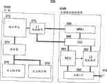
参考图5,基本处理模块是处理器元件(PE)500。PE 500包括I/O接口502、处理单元(PU)504、和多个子处理单元508(即,子处理单元508A、子处理单元508B、子处理单元508C、和子处理单元508D)。本地(或内部的)PE总线512在PU 504、子处理单元508和存储器接口511之间传输数据和应用。本地PE总线512可以具有例如传统结构或者可以被实施为分组交换网络。如果被实现为分组交换网络,尽管需要更多硬件,但是增加了可用带宽。Referring to FIG. 5 , the basic processing module is a processor element (PE) 500 .
可以使用用于实现数字逻辑的各种方法来构造PE 500。然而,PE 500优选地被构造为在硅基板上采用互补金属氧化物半导体的单个集成电路。基板的代替材料包括砷化镓、砷铝化镓以及其他所谓的利用许多种掺杂剂的III-B化合物。也可以使用超导材料,例如,快速单磁通量子(RSFQ)逻辑电路来实现PE 500。The
PE 500通过高带宽存储器连接516与共享(主)存储器514密切关联。尽管存储器514优选地为动态随机存取存储器(DRAM),但是也可以使用其他部件,例如静态随机存取存储器(SRAM)、磁随机存取存储器(MRAM)、光存储器、全息存储器等来实现存储器514。
PU 504和子处理单元508优选地每个耦接到存储器流程控制器(MFC),该存储器流程控制器包括直接存储器存取DMA功能,其与存储器接口511组合、使DRAM 514和PE 500的子处理单元508和PU 504之间的数据交换便利。应该注意,DMAC和/或存储器接口511可以相对于子处理单元508和PU 504集成或分离布置。实际上,DMAC功能和/或存储器接口511功能可以与一个或多个(优选地,所有)子处理单元508和PU 504一起集成。还应该注意,DRAM 514可以相对于PE500集成或分离布置。例如,可以将DRAM514布置在片外,如由所示出的图解所指示的,或者可以以集成的形式将DRAM 514布置在片上。
PU 504可以是,例如能够独立处理数据和应用的标准处理器。在操作中,PU 504优选地调度并指挥子处理单元处理数据和应用。子处理单元优选地是单指令多数据(SIMD)处理器。在PU 504的控制下,子处理器单元以并行且独立的方式执行这些数据和应用的处理。优选地,利用PowerPC核来实现PU 504,PowerPC核是利用精简指令集计算(RISC)技术的微处理器结构。RISC使用简单指令的组合来执行更为复杂的指令。因此,处理器的定时可以基于较简单和较快速的操作,使得微处理器能够在给定的时钟速度下执行更多的指令。
应该注意,可以利用子处理单元508中的起主处理单元作用的一个来实现PU 504,该起主处理单元作用的一个子处理单元调度并指挥子处理单元508进行数据和应用的处理。进一步,可以在处理器元件500内实现多于一个的PU。It should be noted that the
依据该模块化结构,特定计算机系统采用的PE 500的数目是基于那个系统所需要的处理能力的。例如,服务器可以采用四个PE 500,工作站可以利用两个PE 500,PDA可以采用一个PE 500。被分配用来处理特定软件单位(cell)的PE 500的子处理单元的数目取决于该单位之内的程序和数据的复杂度和数量。With this modular structure, the number of PE 500s employed by a particular computer system is based on the processing power required by that system. For example, a server can use four PE 500s, a workstation can use two PE 500s, and a PDA can use one
图6图示了子处理单元(SPU)508的优选结构和功能。SPU 508结构优选地填补通用处理器(被设计用来在一组范围较广的应用上获得高的平均性能)和专用处理器(被设计用来在单个应用上获得高性能)之间的空白。SPU508被设计用来在游戏应用、媒体应用、宽带系统等上获得高性能,用来对实时应用的程序员提供高度控制。SPU 508的一些能力包括:图形几何学流水线(graphics geometry pipeline)/表面剖分(surface subdivision)、快速傅立叶变换、图像处理关键字、流处理、MPEG编码/解码、加密、解密、设备驱动器扩展、建模、游戏物理学(game physics)、内容创建、以及音频合成与处理。FIG. 6 illustrates the preferred structure and functionality of sub-processing unit (SPU) 508 . The
子处理单元508包括两个基本功能单元,即SPU核510A和存储器流程控制器(MFC)510B。SPU核510A执行程序执行、数据处理等,而MFC 510B执行涉及SPU核510A和系统的DRAM 514之间的数据传输的功能。The
SPU核510A包括本地存储器550、指令单元(IU)552、寄存器554、一个或多个浮点执行级556以及一个或多个定点执行级558。优选地,使用单端口随机存取存储器,诸如SRAM来实现本地存储器550。虽然大多数处理器通过采用高速缓存来降低到存储器的等待时间,但是SPU核510A实现相对小的本地存储器550而不是高速缓存。实际上,为了给实时应用(以及这里提及的其他应用)的程序员提供一致的且可预测的存储器访问等待时间,在SPU 508A内不优选高速缓存结构。高速缓存的高速缓存命中/未命中特性产生在几个周期到几百个周期内变化的易变性存储器存取时间。这种易变性消弱了在例如实时应用编程中期望的存取计时的可预测性。通过将DMA传输与数据计算相重叠,可以在本地存储器SRAM 550中实现等待时间隐藏。这为实时应用编程提供了高度控制。由于与DMA传输相关联的等待时间和指令开支超出维护高速缓存未命中的等待时间的开支,所以当DMA传输大小足够大且足够可预测(例如,可以在需要数据之前发出DMA命令)时,SRAM本地存储器方式有利。
在子处理单元508的给定一个上运行的程序使用本地地址来查阅相关联的本地存储器550,然而,本地存储器550的每个位置也被分配有整个系统的存储器映射内的实际地址(RA)。这允许特权软件(privilege software)将本地存储器550映射到处理的有效地址(EA),以使一个本地存储器550和另一本地存储器500之间的DMA传输便利。PU 504也可以直接使用有效地址访问本地存储器500。在优选实施例中,本地存储器550包括556k字节的存储量,以及寄存器552的容量为128×128比特。A program running on a given one of the
优选地,使用处理流水线来实现SPU核504A,在处理流水线中,以流水线形式处理逻辑指令。尽管可以将流水线划分成任何数目的处理指令的级,但是,流水线通常包括:获取一个或多个指令,解码指令,检查指令间的依赖性,发出指令,以及执行指令。鉴于这点,IU 552包括指令缓冲器、指令解码电路、依赖性检查电路、以及指令发出电路。Preferably,
指令缓冲器优选地包括多个寄存器,该多个寄存器耦接到本地存储器550并且可操作用来在获取指令时临时存储它们。优选地,指令缓冲器操作使得所有指令作为一组离开寄存器,即基本上同时地。尽管指令缓冲器可以是任何大小,但是优选的是其具有不大于大约两个或三个寄存器的大小。The instruction buffer preferably includes a plurality of registers coupled to
一般,解码电路分解指令并产生执行对应指令功能的逻辑微操作(micro-operation)。例如,逻辑微操作可以指定算法和逻辑运算、到本地存储器550的加载和存储操作、寄存器源操作数和/或立即数操作数。解码电路还可以指示指令使用哪些资源,诸如目标寄存器地址、结构资源、功能单元和/或总线。解码电路还可以供应指示其中需要资源的指令流水线级的信息。优选地,指令解码电路可操作用来基本上同时地解码数目等于指令缓冲器的寄存器数目的指令。Generally, the decoding circuit decomposes the instructions and generates logical micro-operations (micro-operations) for performing the functions of the corresponding instructions. For example, logical micro-operations may specify arithmetic and logical operations, load and store operations to
依赖性检查电路包括数字逻辑电路,其执行测试以确定给定指令的操作数是否依赖于流水线中的其他指令的操作数。如果依赖,则在更新这些其他操作数(例如,通过许可其他指令完成执行)之前,不能执行给定指令。优选地,依赖性检查电路确定同时从解码器电路发出的多个指令的依赖性。Dependency checking circuitry includes digital logic circuitry that performs tests to determine whether operands of a given instruction are dependent on operands of other instructions in the pipeline. If dependent, a given instruction cannot execute until these other operands are updated (eg, by permitting other instructions to complete execution). Preferably, the dependency checking circuit determines dependencies of a plurality of instructions issued simultaneously from the decoder circuit.
指令发出电路可操作用来向浮点执行级556和/或定点执行级558发出指令。Instruction issue circuitry is operable to issue instructions to floating
优选地,将寄存器554实现为相对大的统一标准的寄存器文件,诸如128项目的寄存器文件。这允许在没有要求寄存器重命名以避免寄存器不足的情况下的深度流水线的(deeply pipelined)高频实现。重命名硬件通常消耗处理系统的相当部分的面积和能力。因此,当软件循环展开或其他交织技术覆盖了等待时间时,则可以实现有利的操作。
优选地,SPU核510A具有超标量结构,使得每个时钟周期发出多于一个指令。优选地,SPU核510A操作为达到对应于从指令缓冲器同时发出的指令的数目、诸如2和3(意味着每个时钟周期发出两个或三个指令)的等级的超标量结构。取决于所需要的处理能力,可以采用或大或小数目的浮点执行级556和定点执行级558。在优选实施例中,浮点执行级556以每秒320亿次浮点运算(32 GFLOPS)的速度操作,以及定点执行级558以每秒320亿次运算(32 GOPS)的速度操作。Preferably,
优选地,MFC 510B包括总线接口单元(BIU)564、存储器管理单元(MMU)562、以及直接存储器存取控制器(DMAC)560。除DMAC 560以外,MFC 510B优选地以与SPU核510A和总线512相比的一半频率(一半速度)运行,以满足低能耗设计目标。MFC 510B可操作用来处理从总线512进入到SPU 508的数据和指令,为DMAC提供地址转换和为数据一致性提供监听操作(snoop-operation)。BIU 564提供在总线512和MMU 562和DMAC 560之间的接口。因此,SPU 508(包括SPU核510A和MFC 510B)和DMAC 560物理和/或逻辑连接到总线512。Preferably, the
优选地,MMU 562可操作用来将有效地址(从DMA命令取得)转换成用于存储器存取的实际地址。例如,MMU 562可以将有效地址的高阶比特转换成实际地址比特。然而,优选地低阶地址比特为不转换的,并且考虑低阶地址比特为逻辑的和物理的两者,以用于形成实际地址和请求到存储器的存取。在一个或多个实施例中,可以基于64比特存储器管理模型来实现MMU 562,并且MMU 562可以提供264字节的有效地址空间,具有4K-、64K-、1M-和16M-字节页大小和256MB段大小。优选地,MMU 562可操作用来为DMA命令支持高达265字节的虚拟存储器、和242字节(4兆兆字节TeraByte)的物理存储器。MMU 562的硬件可以包括8-项目、完全相联的SLB、256-项目、4路组相联TLB、以及用于硬件TLB未命中处理的TLB的4×4替换管理表(RMT)。Preferably, the
优选地,DMAC 560可操作用来管理来自SPU核510A以及诸如PU 504和/或其他SPU的一个或多个其他设备的DMA命令。存在三类DMA命令:Put(放)命令,操作将数据从本地存储器550移动到共享存储器514;Get(取)命令,操作将数据从共享存储器514移动到本地存储器550;存储控制命令,其包括SLI命令和同步命令。同步命令可以包括原子(atomic)命令、发送信号命令、以及专用阻隔(barrier)命令。响应于DMA命令,MMU 562将有效地址转换成实际地址并将实际地址转到BIU 564。Preferably,
优选地,SPU核510A使用通道接口和数据接口,以与DMAC 560内的接口进行通信(发送DMA命令、状态等)。SPU核510A通过通道接口向DMAC 560中的DMA队列发出DMA命令。一旦DMA在DMA队列中,就通过DMAC 560内的发出和完成逻辑电路处理它。当结束DMA命令的所有总线事务时,通过通道接口将完成信号发送回SPU核510A。Preferably,
图7图示PU 504的优选结构和功能。PU 504包括两个基本功能单元,PU核504A和存储器流程控制器(MFC)504B。PU核504A执行程序执行、数据处理、多处理器管理功能等,而MFC 504B执行涉及PU核504A和系统100的存储器空间之间的数据传输的功能。FIG. 7 illustrates the preferred structure and function of
PU核504A可以包括L1高速缓存570、指令单元572、寄存器574、一个或多个浮点执行级576以及一个或多个定点执行级578。L1高速缓存为通过MFC 504B从共享存储器106、处理器102、或存储器空间的其他部分接收到的数据提供数据高速缓存功能。由于优选地将PU核504A实现为超流水线,所以优选地将指令单元572实现为具有许多级(包括获取、解码、依赖性检查、发出等)的指令流水线。优选地,PU核504A也具有超标量配置,由此每时钟周期从指令单元572发出多于一个指令。为了实现高处理能力,浮点执行级576和定点执行级578按流水线配置包括多个级。取决于所需的处理能力,可以采用或多或少数目的浮点执行级576和定点执行级578。
MFC 504B包括总线接口单元(BIU)580、L2高速缓存、不可高速缓存单元(NCU)584、核接口单元(CIU)586、以及存储器管理单元(MMU)588。大多数MFC 504B以与PU核504A和总线108相比的一半频率(一半速度)运行,以满足低能耗设计目标。
BIU 580提供总线108和L2高速缓存582和NCU 584逻辑块之间的接口。为此,BIU 580可以充当为总线108上的主设备以及从设备,从而执行完全一致的存储器操作。作为主设备,其可以代表L2高速缓存582和NCU 584向总线108发出加载/存储请求,以寻求服务。BIU 580还可以实现命令的流程控制机制,其限制可以发送到总线108的命令的总数目。总线108上的数据处理可以被设计为采取八节拍(beat),因此,优选地围绕128字节高速缓存行设计BIU 580,并且一致性和同步粒度为128KB。
优选地,L2高速缓存582(及支持的硬件逻辑电路)被设计用来高速缓存512KB数据。例如,L2高速缓存582可以处理可高速缓存的加载/存储、数据预获取、指令获取、指令预获取、高速缓存操作、以及阻隔操作。优选地,L2高速缓存582为8路组相联系统。L2高速缓存582可以包括匹配六(6)个掷出(castout)队列(例如6个RC机器)的六个重新加载队列、以及八个(64-字节宽)存储队列。L2高速缓存582可以操作以提供L1高速缓存570中的一些或所有数据的备份拷贝。有利地,在处理节点被热交换时,这在恢复存储(多个)状态时是有用的。该配置还允许L1高速缓存570用较少端口更快地操作,并允许较快的高速缓存-到-高速缓存传输(由于请求可能止于L2高速缓存582)。该配置还提供用于将高速缓存一致性管理传到L2高速缓存582的机制。Preferably, L2 cache 582 (and supporting hardware logic) is designed to cache 512KB of data. For example,
NCU 584与CIU 586、L2高速缓存582、以及BIU 580接口,并且通常在PU核504A和存储器系统之间作为用于不可高速缓存的操作的排队/缓冲电路起作用。NCU 584优选地处理不由L2高速缓存582处理的、与PU核504A的所有通信,诸如禁止高速缓存的加载/存储、阻隔操作、以及高速缓存一致性操作。NCU 584优选地以一半速度运行,以满足前述的能耗目标。
CIU 586布置在MFC 504B和PU核504A的边界上,并且充当为来自执行级576、578、指令单元572、以及MMU单元588且去向L 2高速缓存582和NCU 584的请求的路由、仲裁、以及流程控制点。PU核504A和MMU 588优选地以全速运行,而L2高速缓存582和NCU 584可操作用于2:1速度比。因此,在CIU 586中存在频率边界,并且其功能之一是当其在两个频率域之间传递请求和重新加载数据时适当地处理频率交叉。
CIU 586包括三个功能块:加载单元、存储单元以及重新加载单元。另外,CIU 586执行数据预获取功能,优选地该数据预获取功能是加载单元的功能部分。CIU 586优选地可操作用来:(i)从PU核504A和MMU 588接收加载和存储请求;(ii)将请求从全速时钟频率转换成半速(2:1时钟频率转换);(iii)将可高速缓存的请求路由到L2高速缓存582,将不可高速缓存的请求路由到NCU 584;(iv)公平地仲裁到L2高速缓存582和NCU 584的请求;(v)在到L2高速缓存582和NCU 584的分发(dispatch)上提供流程控制,使得在目标窗口内接收请求且避免上溢;(vi)接收加载返回数据并将其路由到执行级576、578、指令单元572或MMU 588;(vii)将监听(snoop)请求传递到执行级576、578、指令单元572或MMU 588;以及(viii)将加载返回数据和监听流量从半速转换为全速。The
优选地,MMU 588为PU核540A提供地址转换,诸如利用第二级地址转换工具。优选地,通过可以比MMU 588小得多且快得多的分离的指令和数据ERAT(有效到实际地址转换)阵列,在PU核504A内提供第一级转换。
在优选实施例中,在64比特实现的情况下,PU 504以46GHz、10F04操作。优选地,寄存器为64比特长(但是一个或多个专用寄存器可能较小一些),并且有效地址为64比特长。优选地,利用PowerPC技术来实现指令单元570、寄存器572以及执行级574和576,以实现(RISC)计算技术。In a preferred embodiment, the
可以在美国专利第6,526,491号中发现关于该计算机系统的模块化结构的额外细节,通过引用将其全部内容融入这里。Additional details regarding the modular architecture of the computer system can be found in US Patent No. 6,526,491, the entire contents of which are incorporated herein by reference.
依据本发明的至少一个进一步的方面,可以利用适合的硬件,诸如在图中图示的硬件,来实现上述方法和装置。可以利用任何已知技术,诸如标准数字电路、可操作用来执行软件和/或固件程序的任何已知处理器、一个或多个可编程数字器件或系统(诸如可编程只读存储器(PROM)、可编程逻辑阵列器件(PAL))等来实现这种硬件。此外,尽管图中图示的装置被示出为被划分到某个功能块中,这种块可以利用分离电路来实现和/或组合成一个或多个功能单元。此外,本发明的各个方面可以利用存储在适合于运输和/或分布的存储介质或媒介(诸如软盘、存储器芯片等)的软件和/或固件程序来实现。According to at least one further aspect of the present invention, the methods and apparatus described above may be implemented using suitable hardware, such as the hardware illustrated in the figures. Any known technology may be utilized, such as standard digital circuitry, any known processor operable to execute software and/or firmware programs, one or more programmable digital devices or systems (such as programmable read-only memory (PROM) , Programmable Logic Array Device (PAL)) etc. to realize this hardware. Furthermore, although the devices illustrated in the figures are shown divided into certain functional blocks, such blocks may be implemented using separate circuits and/or combined into one or more functional units. Furthermore, various aspects of the present invention can be implemented using software and/or firmware programs stored on storage media or media suitable for transportation and/or distribution, such as floppy disks, memory chips, etc.
尽管在这里已经参考具体实施例描述了本发明,但是应该懂得:这些实施例仅仅是本发明的原理和应用的示意。因此,应该懂得:在不偏离如由所附权利要求书限定的本发明的精神和范围的前提下,可以对示意性实施例作出各种修改并且可以开发出其他的布置。Although the invention has been described herein with reference to specific embodiments, it should be understood that these embodiments are merely illustrative of the principles and applications of the invention. It is therefore to be understood that various modifications may be made to the illustrative embodiments and that other arrangements may be developed without departing from the spirit and scope of the invention as defined by the appended claims.
工业实用性Industrial Applicability
本发明可应用于在多处理系统之内传输数据的技术。The invention is applicable to techniques for transferring data within a multiprocessing system.
Claims (17)
Translated fromChineseApplications Claiming Priority (2)
| Application Number | Priority Date | Filing Date | Title |
|---|---|---|---|
| US11/029,891 | 2005-01-05 | ||
| US11/029,891US7698473B2 (en) | 2005-01-05 | 2005-01-05 | Methods and apparatus for list transfers using DMA transfers in a multi-processor system |
Publications (2)
| Publication Number | Publication Date |
|---|---|
| CN101099141A CN101099141A (en) | 2008-01-02 |
| CN100524270Ctrue CN100524270C (en) | 2009-08-05 |
Family
ID=36641981
Family Applications (1)
| Application Number | Title | Priority Date | Filing Date |
|---|---|---|---|
| CNB2006800018526AActiveCN100524270C (en) | 2005-01-05 | 2006-01-05 | Method and apparatus for list transfer using direct memory access transfer in a multiprocessor system |
Country Status (8)
| Country | Link |
|---|---|
| US (1) | US7698473B2 (en) |
| EP (1) | EP1834245B1 (en) |
| JP (1) | JP4346612B2 (en) |
| KR (1) | KR100938942B1 (en) |
| CN (1) | CN100524270C (en) |
| DE (1) | DE602006007944D1 (en) |
| TW (1) | TWI352905B (en) |
| WO (1) | WO2006073204A2 (en) |
Families Citing this family (19)
| Publication number | Priority date | Publication date | Assignee | Title |
|---|---|---|---|---|
| US20070156947A1 (en)* | 2005-12-29 | 2007-07-05 | Intel Corporation | Address translation scheme based on bank address bits for a multi-processor, single channel memory system |
| JP2007207026A (en)* | 2006-02-02 | 2007-08-16 | Matsushita Electric Ind Co Ltd | DMA transfer device |
| JP2008071054A (en)* | 2006-09-13 | 2008-03-27 | Ricoh Co Ltd | Data transfer control method, data processing apparatus, and image processing apparatus |
| US8041847B1 (en) | 2007-05-10 | 2011-10-18 | Marvell International Ltd. | Periodic and conditional execution of DMA operations |
| KR100959136B1 (en) | 2008-07-16 | 2010-05-25 | 한국전자통신연구원 | Direct memory access controller and direct memory access channel data transfer method |
| US9128699B2 (en)* | 2008-12-22 | 2015-09-08 | Intel Corporation | Method and system for queuing transfers of multiple non-contiguous address ranges with a single command |
| JP5423483B2 (en)* | 2010-03-04 | 2014-02-19 | 株式会社リコー | Data transfer control device |
| US10678744B2 (en)* | 2010-05-03 | 2020-06-09 | Wind River Systems, Inc. | Method and system for lockless interprocessor communication |
| KR101706201B1 (en) | 2010-12-15 | 2017-02-15 | 한국전자통신연구원 | Direct memory access controller and operating method thereof |
| US9262163B2 (en) | 2012-12-29 | 2016-02-16 | Intel Corporation | Real time instruction trace processors, methods, and systems |
| KR102306359B1 (en)* | 2015-01-28 | 2021-09-30 | 삼성전자주식회사 | Method and Apparatus for Managing Data Using Processors |
| JP7053891B2 (en)* | 2018-06-27 | 2022-04-12 | シャンハイ カンブリコン インフォメーション テクノロジー カンパニー リミテッド | On-chip code breakpoint debugging method, on-chip processor and breakpoint-based chip debugging system |
| US11121302B2 (en) | 2018-10-11 | 2021-09-14 | SeeQC, Inc. | System and method for superconducting multi-chip module |
| KR102075086B1 (en) | 2018-11-13 | 2020-02-07 | 현대오트론 주식회사 | Epm microtick generation emergency stop using dma |
| US11385820B2 (en)* | 2020-03-04 | 2022-07-12 | Micron Technology, Inc. | Command batching for a memory sub-system |
| CN113849433B (en)* | 2021-09-14 | 2023-05-23 | 深圳市昂科技术有限公司 | Execution method and device of bus controller, computer equipment and storage medium |
| US20250147724A1 (en)* | 2023-11-02 | 2025-05-08 | Flashsilicon Incorporation | Binary floating-point in-memory multiplication device |
| TWI847921B (en)* | 2023-11-22 | 2024-07-01 | 立鴻半導體股份有限公司 | Binary floating-point in-memory multiplication device and operating method thereof |
| CN118226923A (en)* | 2024-05-23 | 2024-06-21 | 深圳市鼎阳科技股份有限公司 | A waveform generator, a waveform generating method and a storage medium |
Citations (4)
| Publication number | Priority date | Publication date | Assignee | Title |
|---|---|---|---|---|
| EP0758824A1 (en)* | 1995-08-15 | 1997-02-19 | Honeywell Inc. | Compact, adaptable, bridging/routing switch |
| US6128674A (en)* | 1997-08-08 | 2000-10-03 | International Business Machines Corporation | Method of minimizing host CPU utilization in driving an adapter by residing in system memory a command/status block a soft interrupt block and a status block queue |
| EP1209573A2 (en)* | 2000-11-22 | 2002-05-29 | Kabushiki Kaisha Toshiba | Multiprocessor system and control method thereof |
| CN1521643A (en)* | 2003-02-13 | 2004-08-18 | 上海汉芯半导体科技有限公司 | Digital Signal Processor with Reconfigurable Channel Count DMA |
Family Cites Families (17)
| Publication number | Priority date | Publication date | Assignee | Title |
|---|---|---|---|---|
| JP2559792B2 (en)* | 1988-02-17 | 1996-12-04 | 日産自動車株式会社 | CAD sketch input drawing method |
| JPH01293431A (en) | 1988-05-23 | 1989-11-27 | Toshiba Corp | Memory access system |
| JPH0736820A (en) | 1993-07-23 | 1995-02-07 | Oki Electric Ind Co Ltd | I/o controller |
| US5617537A (en)* | 1993-10-05 | 1997-04-01 | Nippon Telegraph And Telephone Corporation | Message passing system for distributed shared memory multiprocessor system and message passing method using the same |
| US5634099A (en)* | 1994-12-09 | 1997-05-27 | International Business Machines Corporation | Direct memory access unit for transferring data between processor memories in multiprocessing systems |
| US5644784A (en)* | 1995-03-03 | 1997-07-01 | Intel Corporation | Linear list based DMA control structure |
| JPH1091571A (en) | 1996-09-19 | 1998-04-10 | Fujitsu Ltd | DMA controller chain off detection method and DMA controller |
| JP3484056B2 (en) | 1996-10-18 | 2004-01-06 | 松下電器産業株式会社 | Data transfer device and data transfer system |
| JP3712842B2 (en)* | 1997-08-05 | 2005-11-02 | 株式会社リコー | Data transfer control method, data transfer control device, and information recording medium |
| US6782465B1 (en)* | 1999-10-20 | 2004-08-24 | Infineon Technologies North America Corporation | Linked list DMA descriptor architecture |
| US6529968B1 (en)* | 1999-12-21 | 2003-03-04 | Intel Corporation | DMA controller and coherency-tracking unit for efficient data transfers between coherent and non-coherent memory spaces |
| US6779049B2 (en)* | 2000-12-14 | 2004-08-17 | International Business Machines Corporation | Symmetric multi-processing system with attached processing units being able to access a shared memory without being structurally configured with an address translation mechanism |
| US6526491B2 (en)* | 2001-03-22 | 2003-02-25 | Sony Corporation Entertainment Inc. | Memory protection system and method for computer architecture for broadband networks |
| JP3878508B2 (en) | 2001-11-08 | 2007-02-07 | 松下電器産業株式会社 | Circuit group control system |
| US6804741B2 (en)* | 2002-01-16 | 2004-10-12 | Hewlett-Packard Development Company, L.P. | Coherent memory mapping tables for host I/O bridge |
| JP2004094452A (en)* | 2002-08-30 | 2004-03-25 | Fujitsu Ltd | DMA controller and DMA transfer method |
| US6981072B2 (en)* | 2003-06-05 | 2005-12-27 | International Business Machines Corporation | Memory management in multiprocessor system |
- 2005
- 2005-01-05USUS11/029,891patent/US7698473B2/enactiveActive
- 2006
- 2006-01-05EPEP06702532Apatent/EP1834245B1/enactiveActive
- 2006-01-05KRKR1020077017805Apatent/KR100938942B1/enactiveActive
- 2006-01-05CNCNB2006800018526Apatent/CN100524270C/enactiveActive
- 2006-01-05WOPCT/JP2006/300237patent/WO2006073204A2/enactiveApplication Filing
- 2006-01-05JPJP2006000923Apatent/JP4346612B2/enactiveActive
- 2006-01-05DEDE602006007944Tpatent/DE602006007944D1/ennot_activeExpired - Fee Related
- 2006-01-05TWTW095100561Apatent/TWI352905B/enactive
Patent Citations (4)
| Publication number | Priority date | Publication date | Assignee | Title |
|---|---|---|---|---|
| EP0758824A1 (en)* | 1995-08-15 | 1997-02-19 | Honeywell Inc. | Compact, adaptable, bridging/routing switch |
| US6128674A (en)* | 1997-08-08 | 2000-10-03 | International Business Machines Corporation | Method of minimizing host CPU utilization in driving an adapter by residing in system memory a command/status block a soft interrupt block and a status block queue |
| EP1209573A2 (en)* | 2000-11-22 | 2002-05-29 | Kabushiki Kaisha Toshiba | Multiprocessor system and control method thereof |
| CN1521643A (en)* | 2003-02-13 | 2004-08-18 | 上海汉芯半导体科技有限公司 | Digital Signal Processor with Reconfigurable Channel Count DMA |
Also Published As
| Publication number | Publication date |
|---|---|
| US20060149861A1 (en) | 2006-07-06 |
| EP1834245B1 (en) | 2009-07-22 |
| US7698473B2 (en) | 2010-04-13 |
| TWI352905B (en) | 2011-11-21 |
| JP4346612B2 (en) | 2009-10-21 |
| DE602006007944D1 (en) | 2009-09-03 |
| EP1834245A2 (en) | 2007-09-19 |
| KR20070098900A (en) | 2007-10-05 |
| KR100938942B1 (en) | 2010-01-26 |
| WO2006073204A2 (en) | 2006-07-13 |
| JP2006190301A (en) | 2006-07-20 |
| WO2006073204A3 (en) | 2007-02-08 |
| TW200641624A (en) | 2006-12-01 |
| CN101099141A (en) | 2008-01-02 |
Similar Documents
| Publication | Publication Date | Title |
|---|---|---|
| US7613886B2 (en) | Methods and apparatus for synchronizing data access to a local memory in a multi-processor system | |
| US7526608B2 (en) | Methods and apparatus for providing a software implemented cache memory | |
| JP4421561B2 (en) | Data processing method, apparatus and system for hybrid DMA queue and DMA table | |
| US7882379B2 (en) | Power consumption reduction in a multiprocessor system | |
| US7644255B2 (en) | Method and apparatus for enable/disable control of SIMD processor slices | |
| JP4805341B2 (en) | Method and apparatus for address space virtualization | |
| CN100524270C (en) | Method and apparatus for list transfer using direct memory access transfer in a multiprocessor system | |
| JP4645973B2 (en) | Method, apparatus and system for instruction set emulation | |
| US7689784B2 (en) | Methods and apparatus for dynamic linking program overlay | |
| US7707385B2 (en) | Methods and apparatus for address translation from an external device to a memory of a processor | |
| US20060126770A1 (en) | Methods and apparatus for providing an asynchronous boundary between internal busses in a multi-processor device | |
| WO2006085636A1 (en) | Methods and apparatus for processing instructions in a multi-processor system | |
| CN100419638C (en) | Method and apparatus for improving processing performance using instruction dependency viewing depth | |
| US7818507B2 (en) | Methods and apparatus for facilitating coherency management in distributed multi-processor system |
Legal Events
| Date | Code | Title | Description |
|---|---|---|---|
| C06 | Publication | ||
| PB01 | Publication | ||
| C10 | Entry into substantive examination | ||
| SE01 | Entry into force of request for substantive examination | ||
| C14 | Grant of patent or utility model | ||
| GR01 | Patent grant |