CN100520707C - Method and apparatus for flexible data types - Google Patents
Method and apparatus for flexible data typesDownload PDFInfo
- Publication number
- CN100520707C CN100520707CCN01817951.7ACN01817951ACN100520707CCN 100520707 CCN100520707 CCN 100520707CCN 01817951 ACN01817951 ACN 01817951ACN 100520707 CCN100520707 CCN 100520707C
- Authority
- CN
- China
- Prior art keywords
- data
- operand
- bits
- bit
- data type
- Prior art date
- Legal status (The legal status is an assumption and is not a legal conclusion. Google has not performed a legal analysis and makes no representation as to the accuracy of the status listed.)
- Expired - Fee Related
Links
Images


Classifications
- G—PHYSICS
- G06—COMPUTING OR CALCULATING; COUNTING
- G06F—ELECTRIC DIGITAL DATA PROCESSING
- G06F9/00—Arrangements for program control, e.g. control units
- G06F9/06—Arrangements for program control, e.g. control units using stored programs, i.e. using an internal store of processing equipment to receive or retain programs
- G06F9/30—Arrangements for executing machine instructions, e.g. instruction decode
- G06F9/38—Concurrent instruction execution, e.g. pipeline or look ahead
- G06F9/3824—Operand accessing
- G06F9/383—Operand prefetching
- G—PHYSICS
- G06—COMPUTING OR CALCULATING; COUNTING
- G06F—ELECTRIC DIGITAL DATA PROCESSING
- G06F17/00—Digital computing or data processing equipment or methods, specially adapted for specific functions
- G06F17/10—Complex mathematical operations
- G—PHYSICS
- G06—COMPUTING OR CALCULATING; COUNTING
- G06F—ELECTRIC DIGITAL DATA PROCESSING
- G06F5/00—Methods or arrangements for data conversion without changing the order or content of the data handled
- G—PHYSICS
- G06—COMPUTING OR CALCULATING; COUNTING
- G06F—ELECTRIC DIGITAL DATA PROCESSING
- G06F7/00—Methods or arrangements for processing data by operating upon the order or content of the data handled
- G06F7/38—Methods or arrangements for performing computations using exclusively denominational number representation, e.g. using binary, ternary, decimal representation
- G06F7/48—Methods or arrangements for performing computations using exclusively denominational number representation, e.g. using binary, ternary, decimal representation using non-contact-making devices, e.g. tube, solid state device; using unspecified devices
- G06F7/4806—Computations with complex numbers
- G—PHYSICS
- G06—COMPUTING OR CALCULATING; COUNTING
- G06F—ELECTRIC DIGITAL DATA PROCESSING
- G06F7/00—Methods or arrangements for processing data by operating upon the order or content of the data handled
- G06F7/38—Methods or arrangements for performing computations using exclusively denominational number representation, e.g. using binary, ternary, decimal representation
- G06F7/48—Methods or arrangements for performing computations using exclusively denominational number representation, e.g. using binary, ternary, decimal representation using non-contact-making devices, e.g. tube, solid state device; using unspecified devices
- G06F7/544—Methods or arrangements for performing computations using exclusively denominational number representation, e.g. using binary, ternary, decimal representation using non-contact-making devices, e.g. tube, solid state device; using unspecified devices for evaluating functions by calculation
- G06F7/5443—Sum of products
- G—PHYSICS
- G06—COMPUTING OR CALCULATING; COUNTING
- G06F—ELECTRIC DIGITAL DATA PROCESSING
- G06F7/00—Methods or arrangements for processing data by operating upon the order or content of the data handled
- G06F7/38—Methods or arrangements for performing computations using exclusively denominational number representation, e.g. using binary, ternary, decimal representation
- G06F7/48—Methods or arrangements for performing computations using exclusively denominational number representation, e.g. using binary, ternary, decimal representation using non-contact-making devices, e.g. tube, solid state device; using unspecified devices
- G06F7/57—Arithmetic logic units [ALU], i.e. arrangements or devices for performing two or more of the operations covered by groups G06F7/483 – G06F7/556 or for performing logical operations
- G—PHYSICS
- G06—COMPUTING OR CALCULATING; COUNTING
- G06F—ELECTRIC DIGITAL DATA PROCESSING
- G06F9/00—Arrangements for program control, e.g. control units
- G06F9/06—Arrangements for program control, e.g. control units using stored programs, i.e. using an internal store of processing equipment to receive or retain programs
- G06F9/30—Arrangements for executing machine instructions, e.g. instruction decode
- G06F9/30003—Arrangements for executing specific machine instructions
- G06F9/30007—Arrangements for executing specific machine instructions to perform operations on data operands
- G06F9/3001—Arithmetic instructions
- G06F9/30014—Arithmetic instructions with variable precision
- G—PHYSICS
- G06—COMPUTING OR CALCULATING; COUNTING
- G06F—ELECTRIC DIGITAL DATA PROCESSING
- G06F9/00—Arrangements for program control, e.g. control units
- G06F9/06—Arrangements for program control, e.g. control units using stored programs, i.e. using an internal store of processing equipment to receive or retain programs
- G06F9/30—Arrangements for executing machine instructions, e.g. instruction decode
- G06F9/30003—Arrangements for executing specific machine instructions
- G06F9/30007—Arrangements for executing specific machine instructions to perform operations on data operands
- G06F9/30025—Format conversion instructions, e.g. Floating-Point to Integer, decimal conversion
- G—PHYSICS
- G06—COMPUTING OR CALCULATING; COUNTING
- G06F—ELECTRIC DIGITAL DATA PROCESSING
- G06F9/00—Arrangements for program control, e.g. control units
- G06F9/06—Arrangements for program control, e.g. control units using stored programs, i.e. using an internal store of processing equipment to receive or retain programs
- G06F9/30—Arrangements for executing machine instructions, e.g. instruction decode
- G06F9/30003—Arrangements for executing specific machine instructions
- G06F9/30007—Arrangements for executing specific machine instructions to perform operations on data operands
- G06F9/30032—Movement instructions, e.g. MOVE, SHIFT, ROTATE, SHUFFLE
- G—PHYSICS
- G06—COMPUTING OR CALCULATING; COUNTING
- G06F—ELECTRIC DIGITAL DATA PROCESSING
- G06F9/00—Arrangements for program control, e.g. control units
- G06F9/06—Arrangements for program control, e.g. control units using stored programs, i.e. using an internal store of processing equipment to receive or retain programs
- G06F9/30—Arrangements for executing machine instructions, e.g. instruction decode
- G06F9/30003—Arrangements for executing specific machine instructions
- G06F9/30007—Arrangements for executing specific machine instructions to perform operations on data operands
- G06F9/30036—Instructions to perform operations on packed data, e.g. vector, tile or matrix operations
- G—PHYSICS
- G06—COMPUTING OR CALCULATING; COUNTING
- G06F—ELECTRIC DIGITAL DATA PROCESSING
- G06F9/00—Arrangements for program control, e.g. control units
- G06F9/06—Arrangements for program control, e.g. control units using stored programs, i.e. using an internal store of processing equipment to receive or retain programs
- G06F9/30—Arrangements for executing machine instructions, e.g. instruction decode
- G06F9/30003—Arrangements for executing specific machine instructions
- G06F9/30072—Arrangements for executing specific machine instructions to perform conditional operations, e.g. using predicates or guards
- G—PHYSICS
- G06—COMPUTING OR CALCULATING; COUNTING
- G06F—ELECTRIC DIGITAL DATA PROCESSING
- G06F9/00—Arrangements for program control, e.g. control units
- G06F9/06—Arrangements for program control, e.g. control units using stored programs, i.e. using an internal store of processing equipment to receive or retain programs
- G06F9/30—Arrangements for executing machine instructions, e.g. instruction decode
- G06F9/30098—Register arrangements
- G06F9/30101—Special purpose registers
- G—PHYSICS
- G06—COMPUTING OR CALCULATING; COUNTING
- G06F—ELECTRIC DIGITAL DATA PROCESSING
- G06F9/00—Arrangements for program control, e.g. control units
- G06F9/06—Arrangements for program control, e.g. control units using stored programs, i.e. using an internal store of processing equipment to receive or retain programs
- G06F9/30—Arrangements for executing machine instructions, e.g. instruction decode
- G06F9/30145—Instruction analysis, e.g. decoding, instruction word fields
- G06F9/30149—Instruction analysis, e.g. decoding, instruction word fields of variable length instructions
- G—PHYSICS
- G06—COMPUTING OR CALCULATING; COUNTING
- G06F—ELECTRIC DIGITAL DATA PROCESSING
- G06F9/00—Arrangements for program control, e.g. control units
- G06F9/06—Arrangements for program control, e.g. control units using stored programs, i.e. using an internal store of processing equipment to receive or retain programs
- G06F9/30—Arrangements for executing machine instructions, e.g. instruction decode
- G06F9/30145—Instruction analysis, e.g. decoding, instruction word fields
- G06F9/3016—Decoding the operand specifier, e.g. specifier format
- G06F9/30167—Decoding the operand specifier, e.g. specifier format of immediate specifier, e.g. constants
- G—PHYSICS
- G06—COMPUTING OR CALCULATING; COUNTING
- G06F—ELECTRIC DIGITAL DATA PROCESSING
- G06F9/00—Arrangements for program control, e.g. control units
- G06F9/06—Arrangements for program control, e.g. control units using stored programs, i.e. using an internal store of processing equipment to receive or retain programs
- G06F9/30—Arrangements for executing machine instructions, e.g. instruction decode
- G06F9/30181—Instruction operation extension or modification
- G06F9/30192—Instruction operation extension or modification according to data descriptor, e.g. dynamic data typing
- G—PHYSICS
- G06—COMPUTING OR CALCULATING; COUNTING
- G06F—ELECTRIC DIGITAL DATA PROCESSING
- G06F9/00—Arrangements for program control, e.g. control units
- G06F9/06—Arrangements for program control, e.g. control units using stored programs, i.e. using an internal store of processing equipment to receive or retain programs
- G06F9/30—Arrangements for executing machine instructions, e.g. instruction decode
- G06F9/38—Concurrent instruction execution, e.g. pipeline or look ahead
- G06F9/3802—Instruction prefetching
- G06F9/3808—Instruction prefetching for instruction reuse, e.g. trace cache, branch target cache
- G06F9/381—Loop buffering
- G—PHYSICS
- G06—COMPUTING OR CALCULATING; COUNTING
- G06F—ELECTRIC DIGITAL DATA PROCESSING
- G06F9/00—Arrangements for program control, e.g. control units
- G06F9/06—Arrangements for program control, e.g. control units using stored programs, i.e. using an internal store of processing equipment to receive or retain programs
- G06F9/30—Arrangements for executing machine instructions, e.g. instruction decode
- G06F9/38—Concurrent instruction execution, e.g. pipeline or look ahead
- G06F9/3802—Instruction prefetching
- G06F9/3816—Instruction alignment, e.g. cache line crossing
- G—PHYSICS
- G06—COMPUTING OR CALCULATING; COUNTING
- G06F—ELECTRIC DIGITAL DATA PROCESSING
- G06F9/00—Arrangements for program control, e.g. control units
- G06F9/06—Arrangements for program control, e.g. control units using stored programs, i.e. using an internal store of processing equipment to receive or retain programs
- G06F9/30—Arrangements for executing machine instructions, e.g. instruction decode
- G06F9/38—Concurrent instruction execution, e.g. pipeline or look ahead
- G06F9/3818—Decoding for concurrent execution
- G06F9/382—Pipelined decoding, e.g. using predecoding
- G—PHYSICS
- G06—COMPUTING OR CALCULATING; COUNTING
- G06F—ELECTRIC DIGITAL DATA PROCESSING
- G06F9/00—Arrangements for program control, e.g. control units
- G06F9/06—Arrangements for program control, e.g. control units using stored programs, i.e. using an internal store of processing equipment to receive or retain programs
- G06F9/30—Arrangements for executing machine instructions, e.g. instruction decode
- G06F9/38—Concurrent instruction execution, e.g. pipeline or look ahead
- G06F9/3836—Instruction issuing, e.g. dynamic instruction scheduling or out of order instruction execution
- G06F9/3853—Instruction issuing, e.g. dynamic instruction scheduling or out of order instruction execution of compound instructions
- G—PHYSICS
- G06—COMPUTING OR CALCULATING; COUNTING
- G06F—ELECTRIC DIGITAL DATA PROCESSING
- G06F9/00—Arrangements for program control, e.g. control units
- G06F9/06—Arrangements for program control, e.g. control units using stored programs, i.e. using an internal store of processing equipment to receive or retain programs
- G06F9/30—Arrangements for executing machine instructions, e.g. instruction decode
- G06F9/38—Concurrent instruction execution, e.g. pipeline or look ahead
- G06F9/3877—Concurrent instruction execution, e.g. pipeline or look ahead using a slave processor, e.g. coprocessor
- G—PHYSICS
- G06—COMPUTING OR CALCULATING; COUNTING
- G06F—ELECTRIC DIGITAL DATA PROCESSING
- G06F9/00—Arrangements for program control, e.g. control units
- G06F9/06—Arrangements for program control, e.g. control units using stored programs, i.e. using an internal store of processing equipment to receive or retain programs
- G06F9/30—Arrangements for executing machine instructions, e.g. instruction decode
- G06F9/38—Concurrent instruction execution, e.g. pipeline or look ahead
- G06F9/3885—Concurrent instruction execution, e.g. pipeline or look ahead using a plurality of independent parallel functional units
- G—PHYSICS
- G06—COMPUTING OR CALCULATING; COUNTING
- G06F—ELECTRIC DIGITAL DATA PROCESSING
- G06F7/00—Methods or arrangements for processing data by operating upon the order or content of the data handled
- G06F7/38—Methods or arrangements for performing computations using exclusively denominational number representation, e.g. using binary, ternary, decimal representation
- G06F7/48—Methods or arrangements for performing computations using exclusively denominational number representation, e.g. using binary, ternary, decimal representation using non-contact-making devices, e.g. tube, solid state device; using unspecified devices
- G06F7/499—Denomination or exception handling, e.g. rounding or overflow
- G06F7/49905—Exception handling
- G06F7/4991—Overflow or underflow
- G06F7/49921—Saturation, i.e. clipping the result to a minimum or maximum value
- G—PHYSICS
- G06—COMPUTING OR CALCULATING; COUNTING
- G06F—ELECTRIC DIGITAL DATA PROCESSING
- G06F7/00—Methods or arrangements for processing data by operating upon the order or content of the data handled
- G06F7/38—Methods or arrangements for performing computations using exclusively denominational number representation, e.g. using binary, ternary, decimal representation
- G06F7/48—Methods or arrangements for performing computations using exclusively denominational number representation, e.g. using binary, ternary, decimal representation using non-contact-making devices, e.g. tube, solid state device; using unspecified devices
- G06F7/52—Multiplying; Dividing
- G06F7/523—Multiplying only
- G06F7/53—Multiplying only in parallel-parallel fashion, i.e. both operands being entered in parallel
- G06F7/5318—Multiplying only in parallel-parallel fashion, i.e. both operands being entered in parallel with column wise addition of partial products, e.g. using Wallace tree, Dadda counters
- G—PHYSICS
- G06—COMPUTING OR CALCULATING; COUNTING
- G06F—ELECTRIC DIGITAL DATA PROCESSING
- G06F7/00—Methods or arrangements for processing data by operating upon the order or content of the data handled
- G06F7/38—Methods or arrangements for performing computations using exclusively denominational number representation, e.g. using binary, ternary, decimal representation
- G06F7/48—Methods or arrangements for performing computations using exclusively denominational number representation, e.g. using binary, ternary, decimal representation using non-contact-making devices, e.g. tube, solid state device; using unspecified devices
- G06F7/52—Multiplying; Dividing
- G06F7/523—Multiplying only
- G06F7/533—Reduction of the number of iteration steps or stages, e.g. using the Booth algorithm, log-sum, odd-even
- G06F7/5332—Reduction of the number of iteration steps or stages, e.g. using the Booth algorithm, log-sum, odd-even by skipping over strings of zeroes or ones, e.g. using the Booth Algorithm
Landscapes
- Engineering & Computer Science (AREA)
- Theoretical Computer Science (AREA)
- Software Systems (AREA)
- Physics & Mathematics (AREA)
- General Physics & Mathematics (AREA)
- General Engineering & Computer Science (AREA)
- Mathematical Optimization (AREA)
- Pure & Applied Mathematics (AREA)
- Computational Mathematics (AREA)
- Mathematical Analysis (AREA)
- Computing Systems (AREA)
- Mathematical Physics (AREA)
- Data Mining & Analysis (AREA)
- Algebra (AREA)
- Databases & Information Systems (AREA)
- Advance Control (AREA)
- Complex Calculations (AREA)
- Communication Control (AREA)
- Executing Machine-Instructions (AREA)
Abstract
Translated fromChinese
Description
Translated fromChinese相关申请参考Related application reference
本申请是由发明人Ganapathy等人1999年10月25日提出的美国申请第09/427,174号,律师案卷号第004419.P001的部分继续申请并且本申请要求美国申请09/427,174的优先权,并将其公开内容合并在这里供参考,就象其完全并且完整地在这里被提出一样,两者都要被转让给Vxtel公司。This application is a continuation-in-part of U.S. Application No. 09/427,174, Attorney Docket No. 004419.P001, filed October 25, 1999 by inventor Ganapathy et al. and claims priority to U.S. Application No. 09/427,174, and The disclosure of which is incorporated herein by reference as if set forth herein in its entirety, both of which are assigned to Vxtel Corporation.
本申请还是由发明人Ganapathy等人2000年1月31日提出的美国申请第09/494,608号,律师案卷号第004419.P002的部分继续申请并且本申请要求美国申请09/494,608的优先权,并将其公开内容合并在这里供参考,就象其完全并且完整地在这里被提出一样,两者都要被转让给Vxtel公司。This application is also a continuation-in-part of U.S. Application Serial No. 09/494,608, Attorney Docket No. 004419.P002, filed January 31, 2000 by inventor Ganapathy et al. and this application claims priority to U.S. Application Serial No. 09/494,608, and The disclosure of which is incorporated herein by reference as if set forth herein in its entirety, both of which are assigned to Vxtel Corporation.
技术领域technical field
本发明一般涉及处理器的指令集结构(ISA)。更特别的,本发明涉及用于数字信号处理器的操作数数据类型。The present invention generally relates to the instruction set architecture (ISA) of a processor. More particularly, the present invention relates to operand data types for digital signal processors.
背景技术Background technique
为了在计算设备中处理数据,定义了指令集。具有一个或多个指令的指令集被需要用于如微处理器、计算机或者单一芯片DSP设备等的计算设备。在为计算设备定义指令集时,将被计算的操作数的数据类型通常基于要被利用的数字表示法以及提供的硬件类型被预先定义。指令集结构(ISA)的数据类型本质上通过计算设备将处理哪些类型的数字数据以及如何处理被定义。In order to process data in a computing device, an instruction set is defined. An instruction set of one or more instructions is required for a computing device such as a microprocessor, computer, or single-chip DSP device. When defining an instruction set for a computing device, the data types of the operands to be computed are usually predefined based on the numerical representation to be utilized and the type of hardware provided. The data types of an instruction set architecture (ISA) are essentially defined by which types of digital data a computing device will handle and how.
为数据类型利用的数字表示法包括数的基或基数,无论其是否将被编码(如BCD的二进制编码),以及数字格式。通常被用于计算机的基是二进制或者为2的基数。被用于计算机中的其他基是八进制(8为基),十进制(10为基)以及十六进制(16为基)。如果选择不是2的基数,则通常需要二进制编码因此是数字逻辑可识别的。例如,如果使用10为基数,数字是利用四位二进制数字编码的二进制,其被称为二进制编码的十进制(BCD)。The number representation utilized for the data type includes the base or radix of the number, whether or not it will be encoded (such as BCD's binary encoding), and the number format. The base commonly used in computers is binary or
数字格式与数字是具有定点还是具有浮点表示、整数或小数格式以及其相关表示、标准化还是非标准化格式、以及表示数字的位是压缩的还是复原的相关。在浮点表示中通常包括指数。在定点表示中,小数点(对于基为10的小数点)是在关于位或数据的数字的固定位置。如果小数点在所有数字的右边,则是整数格式。如果小数点在所有数字的左边,则是小数格式。浮点数据格式的一个例子是在IEEE754规范中规定的单精度和双精度浮点数据类型。The number format is related to whether the number has fixed-point or floating-point representation, integer or fractional format and its associated representation, normalized or unnormalized format, and whether the bits representing the number are packed or unpacked. Exponents are often included in floating-point representations. In fixed-point representation, the decimal point (for base 10) is at a fixed position with respect to the number of bits or data. If the decimal point is to the right of all digits, it is an integer format. If the decimal point is to the left of all numbers, it is in decimal format. An example of a floating-point data format is the single-precision and double-precision floating-point data types specified in the IEEE754 specification.
标准化和非标准化格式是浮点表示和小数格式专用的。如果一个数是标准化的,则该数将以小数形式表示并且在小数点右边紧接着的位是1。如果是非标准化格式,则该数将以小数形式表示并且在小数点右边紧接着的位是1或者0。Normalized and denormalized formats are specific to floating-point representation and decimal formats. If a number is normalized, the number is represented in decimal form and the digit immediately to the right of the decimal point is 1. If in non-normalized format, the number will be expressed in decimal form and the digit immediately to the right of the decimal point will be 1 or 0.
如果要被处理的数据可以是正的或者负的,则数字表示需要有编码方案来提供正值和负值两者的表示。用于整数格式的典型的编码方法是符号大小、根值减一的补码(一个数对于二进制或者基为2的补码)以及补码(两个数对于二进制或者基为2的补码)。如果使用浮点格式,则小数值和指数值可以类似于整数编码方法被编码。而且,依赖值的范围和/或想要的精度,需要考虑数字表示的比特(也就是数字)、字节和字的数量。例如,表示一个数的比特的数量可以固定为一个32比特值或者四个8位字节。作为另一个例子,表示一个数的比特的数量可以是对于小数格式为32比特并且对于指数为3比特。If the data to be processed can be positive or negative, digital representations require encoding schemes to provide representation of both positive and negative values. Typical encoding methods for integer formats are sign-size, root minus one's complement (one number to binary or
除此之外,除了数字表示之外,指令集结构的数据类型可包括字符串或数据的文本类型。这种情况下的字符通常被编码为如美国信息交换标准码(ASCII)的二进制格式。编码的另一种形式是扩充的二进制编码的十进制交换码(EBCDIC)。这些编码格式还可以被从其二进制格式压缩为压缩的十进制格式以便减少其表示所需要的比特数量。用于数字信号处理器(DSP)的指令集结构的数据类型非常重要。DSP通常与通用微处理器的区别在于DSP通过包括用于执行数字数的乘法的专门的乘法器和累加器(MAC)典型地支持加速算法运算。典型的DSP设备的指令集通常仅包括一个DSP指令、一个MAC指令,用于执行新操作数的乘法以及与存储在累加器寄存器里的预先累加值的加法。现有技术DSP设备中MAC指令的操作数的数据类型通常依赖于执行其MAC运算部分的乘法器硬件。典型地数据类型对于DSP是固定的。如果想要在具有与数据类型不一致格式的数据的操作数上执行MAC运算,需要执行其他指令来格式化该数据,因此其可以通过具有给定数据类型的给定MAC指令来被处理。这些其他指令包括向存储器中读和写数据以便选择在其上执行MAC指令的操作数的数据的合适的比特。In addition, the data types of the instruction set structure may include character strings or textual types of data in addition to numerical representations. Characters in this case are usually encoded in a binary format such as American Standard Code for Information Interchange (ASCII). Another form of encoding is Extended Binary Coded Decimal Interchange Code (EBCDIC). These encoding formats can also be compressed from their binary format to a compressed decimal format in order to reduce the number of bits required for their representation. The data types used in the instruction set architecture of a digital signal processor (DSP) are very important. DSPs are generally distinguished from general-purpose microprocessors in that DSPs typically support accelerated arithmetic operations by including specialized multipliers and accumulators (MACs) for performing multiplication of digital numbers. The instruction set of a typical DSP device usually consists of only one DSP instruction, one MAC instruction to perform the multiplication of new operands and the addition with the pre-accumulated value stored in the accumulator register. The data type of the operand of the MAC instruction in the prior art DSP device usually depends on the multiplier hardware that executes its MAC operation part. Typically the data types are fixed for the DSP. If one wants to perform a MAC operation on an operand with data in a format inconsistent with the data type, other instructions need to be executed to format the data so it can be processed by a given MAC instruction of the given data type. These other instructions include reading and writing data to memory in order to select the appropriate bits of data for the operands of the MAC instruction on which to execute.
DSP被应用的一个领域是在电信系统中。在电信系统中DSP的一个用途是数字滤波。在这种情况下DSP典型地被用指令编程以便实现数字或时间域中的某个过滤功能。用于典型的有限脉冲响应(FIR)滤波器的数学算法看上去象等式Yn=h0X0+h1X1+h2X2+...+hNXN,其中hn是编号从1到N的固定滤波器系数并且Xn是数据采样。等式Yn可以利用软件程序被估算。但是在有些应用中,等式必须被尽可能快地估算。这样做的一种方式是利用硬件组件如被编程来计算等式Yn的DSP设备来执行计算。为了进一步加快处理,想要矢量化该等式并且将计算分布在多个DSP中因此可以更快地获得最终结果。多个DSP并行运算来加速计算过程。这样,各项的乘法被均衡地扩展到DSP的乘法器用于各项的同时计算。各项的加法类似地被均衡地扩展到DSP的加法器用于同时计算。在矢量化处理中,因为组合是结合的,所以处理项的顺序并不重要。如果各项的处理顺序被改变,对函数的矢量化处理中预计的最终结果没有影响。在被用于执行矢量化处理的DSP设备中,希望考虑在指令集结构的数据类型里考虑矢量化处理的类型以便提高数据处理效率。One area where DSP is used is in telecommunication systems. One use of DSPs in telecommunication systems is digital filtering. In this case the DSP is typically programmed with instructions to implement some filtering function in the digital or time domain. The math for a typical finite impulse response (FIR) filter looks like the equation Yn =h0 X0 +h1 X1 +h2 X2 +...+hN XN , where hn are the fixed filter coefficients numbered from 1 to N and Xn are data samples. The equationYn can be estimated using a software program. But in some applications, the equation must be evaluated as fast as possible. One way of doing this is to use a hardware component such as a DSP device programmed to calculate the equationYn to perform the calculation. To further speed up the processing, one would like to vectorize this equation and distribute the computation across multiple DSPs so the final result can be reached faster. Multiple DSPs operate in parallel to accelerate the calculation process. In this way, the multiplication of terms is evenly extended to the multipliers of the DSP for the simultaneous calculation of terms. The addition of terms is similarly extended to the adders of the DSP for simultaneous calculations. In vectorized processing, the order in which items are processed is not important because the composition is associative. If the order in which items are processed is changed, it has no effect on the expected end result in the function's vectorized processing. In a DSP device used to perform vectorization processing, it is desirable to consider the type of vectorization processing in the data type of the instruction set structure in order to improve data processing efficiency.
通常在通信系统中使用的滤波类型不同。不同类型的滤波系统使用不同类型的操作数和滤波器系数。在这些情况下希望在DSP指令如何处理不同的操作数方面有灵活性。还希望提高使用计算资源的效率来加速DSP指令的执行。There are different types of filtering commonly used in communication systems. Different types of filtering systems use different types of operands and filter coefficients. In these cases it is desirable to have flexibility in how the DSP instructions handle the different operands. It is also desirable to increase the efficiency of using computing resources to speed up the execution of DSP instructions.
发明内容Contents of the invention
本发明提供一种用于利用具有灵活数据类型的操作数执行数字信号处理指令的信号处理器,所述信号处理器包括:The present invention provides a signal processor for executing digital signal processing instructions with operands having flexible data types, the signal processor comprising:
至少一个信号处理单元;at least one signal processing unit;
指令解码器,用来解码数字信号处理指令并读取具有第一数据类型域的第一个操作数、具有第二数据类型域的第二个操作数、和置换域,an instruction decoder for decoding a digital signal processing instruction and reading a first operand having a field of a first data type, a second operand having a field of a second data type, and a permutation field,
其中:in:
该指令解码器用于将第一个操作数的第一数据类型与第二个操作数的第二数据类型进行比较,如果所述指令解码器确定第一个操作数的第一数据类型与第二个操作数的第二数据类型匹配,就使信号处理单元利用第一个操作数和第二个操作数执行DSP指令,而如果所述指令解码器确定第一个操作数的第一数据类型与第二个操作数的第二数据类型不匹配,就执行类型匹配以寻找第一个操作数和第二个操作数的匹配的数据类型,并且使信号处理单元根据匹配的数据类型将第一个和第二个操作数一起对齐,并利用已对齐的第一个和第二个操作数执行DSP指令;以及The instruction decoder is used to compare the first data type of the first operand with the second data type of the second operand, if the instruction decoder determines that the first data type of the first operand is not the same as the second The second data type of the operands matches, causing the signal processing unit to execute the DSP instruction using the first operand and the second operand, and if the instruction decoder determines that the first data type of the first operand is consistent with If the second data type of the second operand does not match, type matching is performed to find the matching data type of the first operand and the second operand, and the signal processing unit converts the first operand according to the matching data type Align with the second operand and execute the DSP instruction with the aligned first and second operands; and
所述至少一个信号处理单元包括数据分类器和对准器,被配置为在第一条数据总线上对齐和可选择地选择一组数据位作为第一个操作数,用于耦合到第一个乘法器或第一个加法器中,所述的一组数据位在第一条数据总线上的对齐和选择响应第一数据类型域。The at least one signal processing unit includes a data sorter and an aligner configured to align and optionally select a set of data bits on a first data bus as a first operand for coupling to a first In the multiplier or the first adder, the alignment and selection of said set of data bits on the first data bus is responsive to the first data type field.
此外,本发明提供一种用于执行具有灵活数据类型的操作数的数字信号处理指令的信号处理器,所述信号处理器包括:Furthermore, the present invention provides a signal processor for executing digital signal processing instructions having operands of flexible data types, the signal processor comprising:
信号处理单元,其中包括被配置为将一对操作数加在一起的第一个加法器和被配置为将一对操作数乘在一起的第一个乘法器;a signal processing unit comprising a first adder configured to add together a pair of operands and a first multiplier configured to multiply together a pair of operands;
指令解码器,用于解码数字信号处理指令并读取具有第一数据类型域的第一个操作数、具有第二数据类型域的第二个操作数、和置换域,an instruction decoder for decoding a digital signal processing instruction and reading a first operand having a field of a first data type, a second operand having a field of a second data type, and a permutation field,
其中:in:
该指令解码器用于将第一个操作数的第一数据类型与第二个操作数的第二数据类型进行比较,如果所述指令解码器确定第一个操作数的第一数据类型与第二个操作数的第二数据类型匹配,就使信号处理单元利用第一个操作数和第二个操作数执行DSP指令,而如果所述指令解码器确定第一个操作数的第一数据类型与第二个操作数的第二数据类型不匹配,就执行类型匹配以寻找第一个操作数和第二个操作数的匹配的数据类型,并且使信号处理单元根据匹配的数据类型将第一个和第二个操作数一起对齐,并利用已对齐的第一个和第二个操作数执行DSP指令。The instruction decoder is used to compare the first data type of the first operand with the second data type of the second operand, if the instruction decoder determines that the first data type of the first operand is not the same as the second The second data type of the operands matches, causing the signal processing unit to execute the DSP instruction using the first operand and the second operand, and if the instruction decoder determines that the first data type of the first operand is consistent with If the second data type of the second operand does not match, type matching is performed to find the matching data type of the first operand and the second operand, and the signal processing unit converts the first operand according to the matching data type Align with the second operand and execute the DSP instruction with the aligned first and second operands.
此外,本发明提供一种信号处理器,用于执行具有灵活数据类型的操作数的数字信号处理指令,所述信号处理器包括:Furthermore, the present invention provides a signal processor for executing digital signal processing instructions having operands of flexible data types, said signal processor comprising:
第一信号处理单元,它具有:A first signal processing unit, which has:
被配置为将第一对操作数加在一起的第一个加法器;a first adder configured to add together the first pair of operands;
被配置为将所述第一对操作数乘在一起的第一个乘法器;以及a first multiplier configured to multiply the first pair of operands together; and
被耦合到第一个加法器和第一个乘法器的第一数据分类器和对准器,第一数据分类器和对准器响应一对数据类型而从多个比特中选出所述的第一对操作数,并将这第一对操作数耦合到第一个加法器和第一个乘法器。A first data sorter and an aligner coupled to the first adder and the first multiplier, the first data sorter and the aligner select from a plurality of bits in response to a pair of data types the first pair of operands, and couple the first pair of operands to the first adder and the first multiplier.
此外,本发明提供一种用于执行具有灵活数据类型的操作数的数字信号处理指令的信号处理器,所述信号处理器包括:Furthermore, the present invention provides a signal processor for executing digital signal processing instructions having operands of flexible data types, the signal processor comprising:
指令解码器,用来解码数字信号处理指令并读取第一数据类型域、第二数据类型域、以及置换域;an instruction decoder for decoding digital signal processing instructions and reading the first data type field, the second data type field, and the permutation field;
多个信号处理单元,它们具有:Multiple signal processing units with:
被配置为将一对操作数加在一起的第一个加法器;a first adder configured to add a pair of operands together;
被配置为将一对操作数乘在一起的第一个乘法器;以及a first multiplier configured to multiply a pair of operands together; and
耦合到第一个加法器和第一个乘法器的数据分类器和对准器,a data sorter and an aligner coupled to the first adder and the first multiplier,
所述数据分类器和对准器被配置为响应第一数据类型域和置换域,而在第一条数据总线上对齐和可选择地选择第一组数据位作为第一个操作数,用于耦合到第一个乘法器或第一个加法器中,而且The data sorter and aligner is configured to align and optionally select a first set of data bits on a first data bus as a first operand responsive to a first data type field and a permutation field for coupled into either the first multiplier or the first adder, and
所述数据分类器和对准器被配置为响应第二数据类型域和置换域,而在第二条数据总线上对齐和可选择地选择第二组数据位作为第二个操作数,用于耦合到第一个乘法器或第一个加法器中。The data sorter and aligner is configured to align and optionally select a second set of data bits on a second data bus as a second operand responsive to a second data type field and a permutation field for Coupled into either the first multiplier or the first adder.
附图说明Description of drawings
图1A是利用本发明的系统的框图。Figure 1A is a block diagram of a system utilizing the present invention.
图1B是在图1A的系统的网关中利用本发明的印制电路板的框图。FIG. 1B is a block diagram of a printed circuit board utilizing the present invention in a gateway of the system of FIG. 1A.
图2是本发明的应用专用信号处理器(ASSP)的框图。Figure 2 is a block diagram of the application specific signal processor (ASSP) of the present invention.
图3是在本发明的ASSP里的核心处理器的实例的框图。Figure 3 is a block diagram of an example of a core processor in an ASSP of the present invention.
图4是在图3的核心处理器中的RISC处理单元的框图。FIG. 4 is a block diagram of a RISC processing unit in the core processor of FIG. 3 .
图5A是在图3的核心处理器里的信号处理单元的实例的框图。FIG. 5A is a block diagram of an example of a signal processing unit in the core processor of FIG. 3 .
图5B是说明信号处理单元的总线结构的图5A的更详细的框图。FIG. 5B is a more detailed block diagram of FIG. 5A illustrating the bus structure of the signal processing unit.
图6是用于本发明的指令集结构的操作数的通用数据类型格式。Figure 6 is a general data type format for operands of the instruction set architecture of the present invention.
图7是用于控制寄存器的说明操作数的数据分类(typing)和置换的示例位图。Figure 7 is an example bitmap illustrating data typing and permutation of operands for a control register.
图8是可以被选择的可能数据类型的操作数的示例图。Fig. 8 is an example diagram of operands of possible data types that may be selected.
图9是操作数的可能的置换以及其对于信号处理单元各自的方位的示例图。Figure 9 is an example diagram of possible permutations of operands and their respective orientations to the signal processing unit.
图10是图3的每个信号处理单元的数据分类器(typer)和对准器的横截面的框图。FIG. 10 is a block diagram of a cross-section of a data typer and an aligner of each signal processing unit of FIG. 3 .
图11是在图10的每个信号处理单元的数据分类器和对准器中包含的总线多路复用器的框图。FIG. 11 is a block diagram of a bus multiplexer included in the data sorter and aligner of each signal processing unit of FIG. 10 .
图12A是用于信号处理单元的加法器的实数类型及其对齐的图表。Fig. 12A is a diagram of the real type and its alignment for the adder of the signal processing unit.
图12B是用于信号处理单元的乘法器的实数类型及其对齐的图表。Figure 12B is a diagram of the real number types and their alignment for the multipliers of the signal processing unit.
图12C是用于信号处理单元的加法器的复数类型及其对齐的第一个图表。Fig. 12C is a first diagram of the complex type and its alignment for the adder of the signal processing unit.
图12D是用于信号处理单元的加法器的复数类型及其对齐的第二个图表。Fig. 12D is a second diagram of the complex type and its alignment for the adder of the signal processing unit.
图12E是用于信号处理单元的乘法器的复数类型及其对齐的图表。Figure 12E is a diagram of the complex type of multipliers and their alignment for the signal processing unit.
图12F是用于信号处理单元的乘法器的复数类型及其对齐的第二个图表。Figure 12F is a second diagram of the complex type and alignment of the multipliers for the signal processing unit.
图13A是说明与一对实数操作数匹配的数据类型的图表。Figure 13A is a diagram illustrating data types that match a pair of real operands.
图13B是说明与一对复数操作数匹配的数据类型的图表。Figure 13B is a diagram illustrating the data types that match a pair of complex operands.
图13C是说明与一个实数操作数和一个复数操作数匹配的数据类型的图表。Fig. 13C is a diagram illustrating data types matching a real operand and a complex operand.
图14是说明与信号处理单元的乘法器匹配的数据类型的示例图表。FIG. 14 is an example diagram illustrating a data type matched to a multiplier of a signal processing unit.
图15A是说明用于标量加法的信号处理单元的加法器匹配的数据类型的示例图表。15A is an example diagram illustrating data types for adder matching of a signal processing unit for scalar addition.
图15B是说明用于矢量加法的信号处理单元的加法器匹配的数据类型的示例图表。15B is an example diagram illustrating data types for adder matching of a signal processing unit for vector addition.
图16是在每个信号处理单元的数据分类器和对准器中包含的总线多路复用器的控制的框图。Fig. 16 is a block diagram of the control of the bus multiplexer included in the data sorter and aligner of each signal processing unit.
附图中相同的参考数字和名称指示提供类似功能的元件。参考指示符数字后面的字母表示具有该参考指示符数字的元件的一个实例。Like reference numbers and names in the figures indicate elements providing similar functions. A letter following a reference designator number indicates an example of an element having that reference designator number.
具体实施方式Detailed ways
在本发明下面的详细描述中,提出许多特定细节以便提供对本发明的彻底理解。但是,对于本领域的技术人员很显然本发明可以在没有这些特定细节的情况下实行。在其他实例中众所周知的方法、过程、组件和电路没有被详细描述以便不使得不必要地使本发明的方面变得模糊。而且,本发明将在特定实施方案中被描述但是可在硬件、软件、固件或者其组合中实现。In the following detailed description of the invention, numerous specific details are set forth in order to provide a thorough understanding of the invention. It will be apparent, however, to one skilled in the art that the present invention may be practiced without these specific details. In other instances well-known methods, procedures, components and circuits have not been described in detail so as not to unnecessarily obscure aspects of the invention. Furthermore, the invention will be described in specific embodiments but may be implemented in hardware, software, firmware or a combination thereof.
具有本发明的指令集结构的多个应用专用信号处理器(ASSP)包括操作数的灵活的数据分类、置换以及类型匹配。操作数的灵活的数据分类、置换以及类型匹配提供编程的灵活性以便支持具有不同类型滤波器系数或数据采样的不同的滤波和DSP算法。支持通信系统的网关里不同的DSP算法的灵活性提供分组化网络上改善的语音和数据通信。每个ASSP包括串口、缓存和四个核心处理器以便同时处理多个语音或数据信道。每个核心处理器优选的包括精简指令集计算机(RISC)处理器以及四个信号处理单元(SP)。每个SP包括多个算法块来同时处理多个语音和数据通信信号采样用于在IP、ATM、帧中继或其他分组化网上通信。四个信号处理单元可以并行执行数字信号处理算法。每个ASSP是灵活的并且可以被简单地通过改变控制ASSP执行的命令的软件程序而编程来执行许多网络功能或者数据/语音处理功能,包括电信系统(如CODEC),特别是分组化电信网中的语音和数据压缩/解压缩。Multiple Application Specific Signal Processors (ASSPs) with the instruction set architecture of the present invention include flexible data sorting, permutation, and type matching of operands. Flexible data sorting, permutation, and type matching of operands provide programming flexibility to support different filtering and DSP algorithms with different types of filter coefficients or data samples. The flexibility to support different DSP algorithms in the gateway of the communication system provides improved voice and data communication over packetized networks. Each ASSP includes a serial port, cache, and four core processors to handle multiple voice or data channels simultaneously. Each core processor preferably includes a Reduced Instruction Set Computer (RISC) processor and four Signal Processing Units (SP). Each SP includes multiple algorithm blocks to simultaneously process multiple voice and data communication signal samples for communication over IP, ATM, Frame Relay, or other packetized networks. Four signal processing units can execute digital signal processing algorithms in parallel. Each ASSP is flexible and can be programmed to perform many network functions or data/voice processing functions, including telecommunications systems (such as CODECs), especially in packetized telecommunications networks, simply by changing the software program that controls the commands executed by the ASSP voice and data compression/decompression.
ASSP的指令集结构适合于包括如压缩/解压缩和回声消除的音频和语音处理的数字信号处理应用。利用ASSP实现的指令集结构适合于DSP算法结构。本发明的ISA对DSP算法结构的这种适应平衡了易于实现、处理效率以及DSP算法的可编程性。指令集结构可以被看作为两个组件部分,一个(RISC ISA)对应于RISC控制单元并且另一个(DSPISA)对应于信号处理单元300的DSP数据路径。RISC ISA是在寄存器文件413中包括16寄存器的基于寄存器的结构,而DSP ISA是具有有效数字信号处理指令的基于存储器的结构。ASSP的指令字典型地是20位,但是可以被扩展到40位来控制两个指令串行或并行地执行,如两个RISC控制指令和扩展DSP指令。ASSP的指令集结构有四种不同类型的指令来优化DSP运算混合。这些是(1)使用控制寄存器(也就是模式寄存器)中的模式位的20位DSP指令,(2)具有可以取代模式寄存器的控制扩展的40位DSP指令,(3)20位二元DSP指令,(4)40位二元DSP指令。这些指令是用于加速该类型的核心处理器里的计算的指令,其中D=[(A op1 B)op2 C]并且每个“op1”和“op2”可以是三个操作数A、B、C上的乘、加或极值(最小/最大)运算类。加速这些计算的ASSP的ISA允许操作的不同组合的有效链接。The ASSP's instruction set architecture is suitable for digital signal processing applications including audio and speech processing such as compression/decompression and echo cancellation. The instruction set structure realized by ASSP is suitable for DSP algorithm structure. This adaptation of the ISA of the present invention to the structure of DSP algorithms balances ease of implementation, processing efficiency, and programmability of DSP algorithms. The instruction set structure can be seen as two component parts, one (RISC ISA) corresponding to the RISC control unit and the other (DSPISA) corresponding to the DSP data path of the
ASSP的指令集结构的所有DSP指令是在一个指令中利用一个周期处理量执行两个运算的二元DSP指令。二元DSP指令是在一个指令中两个DSP指令或运算的组合并且包括主DSP运算(MAIN OP)以及子DSP运算(SUB OP)。一般的,本发明的指令集结构可被概括为组合任何一对基本的DSP运算以便提供非常强大的二元指令组合。优选实施方案中的DSP算法运算包括乘法指令(MULT)、加法指令(ADD)、也被称为极值指令的最小/最大指令(MIN/MAX),以及空操作指令(NOP),每个有相关的运算代码(“opcode”)。All DSP instructions of ASSP's instruction set structure are binary DSP instructions that execute two operations with one cycle throughput in one instruction. A binary DSP instruction is a combination of two DSP instructions or operations in one instruction and includes a main DSP operation (MAIN OP) and a sub DSP operation (SUB OP). In general, the instruction set architecture of the present invention can be generalized to combine any pair of basic DSP operations to provide a very powerful combination of binary instructions. The DSP arithmetic operations in the preferred embodiment include multiply instructions (MULT), add instructions (ADD), minimum/maximum instructions (MIN/MAX), also known as extremum instructions, and no-operation instructions (NOP), each with The associated operation code ("opcode").
本发明利用应用专用信号处理器的指令集结构以及硬件结构来有效地执行这些二元DSP指令。The present invention utilizes the instruction set structure and hardware structure of the application-specific signal processor to effectively execute these binary DSP instructions.
现在参见图1A,说明了语音和数据通信系统100。系统100包括是分组化或分组交换网,如IP、ATM或帧中继的网络101。网络101允许在系统100的端点之间利用分组进行语音/话音和数据通信。数据可以是包括音频、视频、电子邮件和其他一般数据形式的任何类型。在系统100的每一端,当通过网络101收发时,语音或数据需要分组化。系统100包括网关104A、104B以及104C以便将接收的信息进分组化用于在网络101上发送。网关是用于连接使用不同协议的多个网络和设备的设备。语音和数据信息可以从多个不同的源以各种数字格式提供给网关104。在系统100中,模拟语音信号由电话108收发。在系统100中,数字语音信号在耦合到多个电话、传真机或数据调制解调器的公共分支交换机(PBX)112A和112B处被收发。数字语音信号在PBX 112A和PBX 112B之间分别通过网关104A和104C收发。数字数据信号还可以在数字调制解调器114和网关104A之间直接收发。数字调制解调器114可以是数字用户线(DSL)调制解调器或者电缆调制解调器。数据信号还可以利用无线地将数字信号或模拟信号收发到基站116的移动单元118来通过无线通信系统耦合到系统100。基站116将模拟信号转换为数字信号或者直接将数字信号传递到网关104B。数据可以利用调制解调器110在普通老式电话系统(POTS)107B上利用调制解调器信号收发。在POTS 107B上通信的调制解调器信号传统地实际上是模拟的并且耦合到公共交换电话网(PSTN)的交换机106B。在交换机106B,来自POTS 107B的模拟信号被数字化并且通过时分复用(TDM)被收发到网关104B,每个时隙表示一个信道和到网关104B的一个DS0输入。在网关104A、104B和104C的每个,进入信号被分组化用于在网络101上发送。由网关104A、104B和104C从网络101接收的信号被去分组化并且转换代码以便发送到合适的目的地。Referring now to FIG. 1A, a voice and
现在参见图1B,说明了网关104的网络接口卡(NIC)130。NIC 130包括一个或多个应用专用信号处理器(ASSP)150A-150N。网关中ASSP的数量是可扩展的以便处理额外的信道。NIC 130的线路接口设备131向连接到网关的各种设备,包括网络101提供接口。在对网络101接口中,线路接口设备将数据分组化用于在网络101上发送出去并且将要被ASSP设备接收的数据去除分组化。线路接口设备131处理由网关在接收总线134上接收的信息并且将其提供给ASSP设备。来自ASSP设备150的信息在发送总线132上通信用于发送到网关之外。传统的线路接口设备是多信道串行接口或UTOPIA设备。NIC 130耦合到网关104里的网关底板/网络接口总线136。桥逻辑138在总线136和NIC 130之间收发信息。桥逻辑138将NIC 130和底板/网络接口总线136之间的信号收发到主总线139上用于通信到ASSP设备150A-150N的一个或多个、主处理器140或者主存储器142。任选地耦合到一个或多个ASSP设备150A到150N(一般称为ASSP 150)的每个的分别是可选的本地存储器145A到145N(一般称为可选本地存储器145)。接收总线134和发送总线132上的数字数据优选地以位宽的形式通信。虽然每个ASSP里的内部存储器足够大到被用做暂时存储器,但是如果额外的存储器空间是必要的,则可选本地存储器145可由每个ASSP 150使用。Referring now to FIG. 1B , network interface card (NIC) 130 of gateway 104 is illustrated.
每个ASSP 150为网关提供信号处理功能。因为每个ASSP可执行不同的信号处理程序,所以提供的信号处理类型是灵活的。ASSP的典型的信号处理和相关的语音分组化功能包括(a)回声消除;(b)视频、音频、以及语音/话音压缩/解压缩(语音/话音编码和解码);(c)延迟处理(分组,帧);(d)丢失处理;(e)连接性(LAN和WAN);(f)保密性(加密/解密);(g)电话接通性;(h)协议处理(保留和传输协议,用于IP的RSVP、TCP/IP、RTP、UDP、以及用于ATM的AAL2、AAL1、AAL5);(i)过滤;(j)无声抑制;(k)长度处理(帧、分组);以及与通信系统上语音和数据通信相关的其他数字信号处理功能。每个ASSP 150可以执行其他功能以便在分组化网上将分组数据流中的语音和数据发送到系统100的各种端点。Each
现在参见图2,说明了ASSP 150的框图。在ASSP 150的中心是四个核心处理器200A-200D。核心处理器200A-200D的每个通过总线203A-203D分别耦合到数据存储器202A-202D。核心处理器200A-200D的每个还分别通过总线205A-205D分别耦合到程序存储器204A-204D。核心处理器200A-200D的每个通过多信道串口206、多信道存储器移动引擎208、缓存210和数据存储器202A-202D与外部信道通信。ASSP 150还包括外部存储器接口212来耦合到外部可选本地存储器145。ASSP150包括外部主机接口214用于接口到图1B的外部主处理器140。在ASSP 150中还包括定时器216、时钟生成器和锁相环218、杂项控制逻辑220以及用于边界扫描测试的联合测试行动组(JTAG)测试接入端口222。对于如ATM的某些应用,多信道串行接口206可被UTOPIA并行接口替换。ASSP 150还包括微控制器223以便执行对于核心处理器200A-200D的处理时序安排以及在ASSP里数据移动的协调,还有中断控制器224来辅助中断处理以及ASSP 150的控制。Referring now to FIG. 2, a block diagram of the
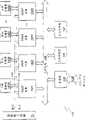
现在参见图3,说明了通过总线203耦合到其相应的数据存储器202以及通过总线205耦合到程序存储器204的核心处理器200的框图。核心处理器200是核心处理器200A-200D的每个的框图。数据存储器202和程序存储器204指数据存储器202A-202D和程序存储器204A-204D的各自的一个实例。总线203和205分别指总线203A-203D和205A-205D各自的实例。核心处理器200包括四个信号处理单元SP0300A、SP1 300B、SP2 300C以及SP3 300D。核心处理器200还包括精简指令集计算机(RISC)控制单元302和管道控制单元304。信号处理单元300A-300D在数据上执行信号处理任务而RISC控制单元302和管道控制单元304执行与由SP 300A-300D执行的信号处理功能相关的控制任务。由RISC控制单元302提供的控制在管道层与SP 300A-300D耦合以便生成紧密集成的核心处理器200来保持在一个非常高的水平上利用信号处理单元200。Referring now to FIG. 3 , there is illustrated a block diagram of
程序存储器204耦合到包括指令缓存作为本地循环缓存的管道控制304。优选实施方案中的指令缓存有保留四个指令的功能。管道控制304的指令缓存减少了在程序循环执行期间访问主存储器以便取指令方面所消耗的能量。
信号处理任务在信号处理单元300A-300D里的数据路径上被执行。DSP算法的特性是它们是在数据流上固有的矢量运算,具有最小的临时位置(数据重用)。因此,不使用具有请求页式调度的数据缓存,因为其不能很好地起作用并且会降低操作性能。因此,在没有发布许多负载并且将指令存储在存储器中的情况下,信号处理单元300A-300D被允许从数据存储器202直接访问矢量元素(操作数),导致非常高效的数据处理。因此,具有可以扩展为40位指令字的20位指令字的本发明的指令集结构,通过使ISA适合DSP算法结构,比利用256位或更高的指令宽度的VLIW结构获得了更好的效率。适合的ISA导致可以调整为更高计算需要的非常紧凑并且低功率的硬件。ASSP可以容纳的操作数的数据类型和数据大小可以改变。数据类型可以是实数或复数、整数或分数,具有不同大小的多个元素的矢量。在优选实施方案中数据大小是64位但是通过正确的指令编码可以容纳更大的数据大小。Signal processing tasks are performed on the data paths within the
现在参见图4,说明了RISC控制单元302的详细框图,RISC控制单元302包括数据对准器和格式器402、存储器地址生成器404、三个加法器406A-406C、算法逻辑单元(ALU)408、乘法器410、桶形移位器412、以及寄存器文件413。寄存器文件413指向开始存储器位置,从此存储器地址生成器404可以将地址生成到数据存储器202中。RISC控制单元302负责将地址提供给数据存储器因此正确的数据流被送入信号处理单元300A-300D。RISC控制单元302是寄存具有负载的组织并且存储指令的寄存器以便将数据移入或移出数据存储器202。数据存储器寻址由RISC控制单元执行,其利用32位寄存器作为指针确定地址、修改后偏移、以及类型和置换域。类型域允许各种固有的DSP数据被支持作为结构中的“头等公民”。例如,复数类型允许在存储在存储器中的复数数据上直接运算,去掉了许多簿记指令。这在高效地支持数据调制解调器中的QAM解调器中非常有用。Referring now to FIG. 4, there is illustrated a detailed block diagram of
现在参见图5A,说明了信号处理单元300的框图,其代表SP300A-300D的一个实例。每个信号处理单元300包括数据分类器和对准器502、第一乘法器Mi504A、压缩器506、第一加法器A1 510A、第二加法器A2 510B、累加寄存器512、第三加法器A3 510C、以及第二乘法器M2 504B。加法器510A-510C在结构上是类似的并且一般称为加法器510。乘法器504A和504B在结构上是类似的并且一般称为乘法器504。乘法器504A和504B的每个在其输入阶段分别有多路复用器514A和514B将来自不同总线的不同输入多路复用到乘法器中。地址510A、510B、510C的每个在其输入阶段也分别具有多路复用器520A、520B、520C将来自不同总线的不同输入多路复用到加法器中。这些多路复用器和其他控制逻辑允许加法器、乘法器和信号处理单元300A-300C中的其他组件通过多路复用器正确的选择灵活地互连。在优选实施方案中,乘法器M1 504A、压缩器506、加法器A1 510A和加法器A2510B,以及累加器512,可以通过数据分类器和对准器502直接从外部数据总线接收输入。在优选实施方案中,加法器510C和乘法器M2 504B接收来自累加器512的输入或者来自执行单元乘法器M1 504A、压缩器506、加法器A1 510A以及加法器A2 510B的输出。Referring now to FIG. 5A, there is illustrated a block diagram of
现在参见图5B,说明了信号处理单元300的功能块和总线结构的更详细的框图。因为在每个信号处理单元中提供了结构和功能性,所以灵活的数据分类是可能的。到数据存储器202的总线203包括Z输出总线532和X输入总线531以及Y输入总线533。输出信号通过数据分类器和对准器502在Z输出总线532上被耦合到信号处理器300之外。输入信号通过数据分类器和对准器502在X输入总线531和Y输入总线533上被耦合到信号处理器300里。两个操作数可以被一起从数据存储器202并行加载到信号处理器300中,X总线531和Y总线533每个上一个。Referring now to FIG. 5B , a more detailed block diagram of the functional blocks and bus structure of the
信号处理器300内部,SXM总线552和SYM总线556分别在数据分类器和对准器502以及乘法器M1 504A之间耦合用于来自X总线531和Y总线533的两个操作数源。SXA总线550和SYA总线554分别在数据分类器和对准器502和加法器A1 510A之间以及数据分类器和对准器502和加法器A2510B之间耦合用于来自X总线531和Y总线533的两个操作数源。在优选实施方案中,X总线531和Y总线533是64位宽而SXA总线550和SYA总线554是40位宽并且SXM总线552和SYM总线556是16位宽。另一对内部总线在数据分类器和对准器502和压缩器506之间以及数据分类器和对准器502和累加寄存器AR 512之间耦合。虽然数据分类器和对准器502可以有耦合到加法器A3 510C和乘法器M2 504B的数据总线,在优选实施方案中其没有这样,以便避免外部数据线以及保存集成电路的区域使用。输出数据被在另一总线上从累加寄存器AR 512耦合到数据分类器和对准器502。乘法器M1504A有总线将其输出耦合到压缩器506、加法器A1 510A、加法器A2510B、以及累加寄存器AR 512的输入。压缩器506有总线将其输出耦合到加法器A1 510A和加法器A2 510B的输入。加法器A1 510A有总线将其输出耦合到累加寄存器512。加法器A2 510B有总线将其输出耦合到累加寄存器512。累加寄存器512有总线将其输出耦合到乘法器M2 504B、加法器A3 510C、以及数据分类器和对准器502。加法器A3 510C有总线将其输出耦合到乘法器M2 504B、累加寄存器512。乘法器M2504B有总线将其输出耦合到加法器A3 510C和累加寄存器AR 512的输入。Inside
指令集结构instruction set structure
ASSP 150的指令集结构适合于包括音频和语音处理,如压缩/解压缩和回声消除的数字信号处理应用。本质上,利用ASSP 150实现的指令集结构适合于DSP算法结构。本发明的ISA对DSP算法结构的这种适应是易于实现、处理效率以及DSP算法的可编程性之间的平衡。本发明的ISA提供了数据移动运算、DSP/算法/逻辑运算、程序控制运算(如功能调用/返回、无条件/条件跳转和分支)、以及系统运算(如特权、中断/陷阱/危险处理以及存储器管理控制)。The instruction set architecture of the
ASSP 150的指令集结构可被看作是两个组件部分,一个(RISC ISA)对应于RISC控制单元并且另一个(DSP ISA)对应于信号处理单元300的DSP数据路径。RISC ISA是基于寄存器的结构,在寄存器文件413中包括十六个寄存器,而DSP ISA是具有有效数字信号处理指令的基于存储器的结构。ASSP的指令字典型的是20位但是可以被扩展到40位以便控制两个RISC或DSP指令来被串行或并行地执行,如RISC控制指令被与DSP指令、或者40位扩展RISC或者DSP指令并行执行。The instruction set structure of the
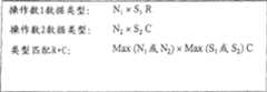
ASSP 150的指令集结构有四种不同类型的指令来优化DSP运算混合。这些是(1)使用控制寄存器(也就是模式寄存器)中的模式位的20位DSP指令,(2)具有可以取代模式寄存器的控制扩展的40位DSP指令,(3)20位二元DSP指令,(4)40位二元DSP指令。这些指令是用于加速该类型的核心处理器里的计算,其中D=[(A op1 B)op2 C]并且每个“op1”和“op2”可以是三个操作数A、B、C上的乘、加、极值(最小/最大)或者其他基本的运算类。加速这些计算的ASSP的ISA允许操作的不同组合的有效链接。这些运算类型需要三个操作数,其对于要执行该运算的处理器需要可用。集成电路的大小在总线结构上加有限制,其将带宽限制为每个周期从数据存储器202中读出两个矢量和向数据存储器写入一个矢量。因此三个操作数之一,如B或C,需要来自核心处理器200的另一个源。第三个操作数可以被放入累加器512或者RISC寄存器文件413的寄存器之一。为了在核心处理器200里实现这一点,有两个20位DSP指令的子类:(1)由4位说明符指定的A和B,以及由1位说明符指定的C和D以及(2)由4位说明符指定的A和C,以及由1位说明符指定的B和D。The
ASSP的指令总是一次从程序存储器中取出40位,位39和19指示指令类型。取出之后,该指令被分组成每个20位的两部分用于执行运算。在20位控制指令并行执行的情况下(位39=0,位19=0),两个20位部分是被同时执行的控制指令。在20位控制指令串行执行的情况下(位39=0,位19=1),两个20位部分是被连续执行的控制指令。在20位DSP指令串行执行的情况下(位39=1,位19=1),两个20位部分是被连续执行的DSP指令。在40位扩展DSP指令的情况下(位39=1,位19=0),两个20位部分形成一个被同时执行的扩展DSP指令。ASSP instructions always fetch 40 bits from program memory at a time, and
ASSP 150的ISA被完全预测提供执行预测。在20位RISC控制指令字和40位扩展DSP指令字中,每个指令有两位指定RISC控制单元302里的四个预测寄存器之一。依赖于预测寄存器的情况,指令执行可以基于其内容有条件地改变。The ISA of
为了访问数据存储器202中的操作数或者累加器512的寄存器或寄存器文件413,在DSP扩展指令中使用6位说明符来访问存储器和寄存器中的操作数。在扩展的DSP指令中使用的六位说明符的MSB(位5)指示访问是存储器访问还是寄存器访问。在优选实施方案中,如果位5被设置为逻辑一,则其表示操作数的存储器访问。如果位5被设置为逻辑零,则其表示操作数的寄存器访问。如果位5被设置为1,则指定寄存器的内容(rX其中X:0-7)被用于获得有效的存储器地址并且由在指定的rX寄存器之一中指定的两个可能的偏移之一来后修改指针域。如果位5被设置为0,则位4确定什么寄存器设置有想要的操作数的内容。如果位4被设置为0,则剩余的指定位3:0控制对寄存器文件413里的寄存器、或者信号处理单元300的寄存器的访问。To access operands in
DSP指令DSP instruction
ASSP150主要有四类DSP指令:ASSP150 mainly has four types of DSP instructions:
1)乘法(MULT):控制从存储器连接到数据总线的主乘法器的执行。1) Multiplication (MULT): Controls the execution of the main multiplier connected from the memory to the data bus.
控制:舍入,乘法符号Controls: rounding, multiplication sign
在通过地址寄存器中的类型域指定的矢量数据上运算Operates on vector data specified by the type field in the address register
第二运算:矢量或标量模式的Add、Sub、Min、MaxSecond operation: Add, Sub, Min, Max in vector or scalar mode
2)加法(ADD):控制主加法器的执行2) Addition (ADD): Control the execution of the main adder
控制:输入的绝对值控制,限制结果Control: Absolute value control of input, limit result
第二运算:Add、add-sub、mult、mac、min、maxSecond operation: Add, add-sub, mult, mac, min, max
3)极值(MIN/MAX):控制主加法器的执行3) Extreme value (MIN/MAX): Control the execution of the main adder
控制:输入的绝对值控制,通过T寄存器、TR寄存器记录控制的全局或运行max/minControl: Absolute value control of the input, record the global or run max/min of the control through the T register and the TR register
第二运算:add、sub、mult、mac、min、maxSecond operation: add, sub, mult, mac, min, max
4)杂类:类型匹配和置换运算4) Miscellaneous: type matching and replacement operations
ASSP 150可以以矢量或者标量方式执行这些DSP算法运算。在标量执行中,减少或合并运算在矢量结果上执行以便生成标量结果。在DSP应用中通常执行标量运算,其可以被ASSP 150高效地执行。
20位DSP指令字有可以利用RISC控制单元302的寄存器文件413里的8个地址寄存器(r0-r7)直接访问数据存储器的4位操作数说明符。20位DSP指令字的寻址方法是定期地间接地址寄存器将指针指定到存储器、后修改值、访问的数据类型以及高效执行该算法所需的数据的置换。所有的DSP指令控制乘法器504A-504B、加法器510A-510C、压缩器506和累加器512、每个信号处理单元300A-300D的功能单元。The 20-bit DSP instruction word has a 4-bit operand specifier that can directly access data memory using the 8 address registers (r0-r7) in the
在40位指令字中,从20位指令字的类型扩展分成五类:In the 40-bit instruction word, the type extension from the 20-bit instruction word is divided into five categories:
1)取代模式寄存器中的控制位的控制和说明符扩展1) Control and specifier extensions that replace the control bits in the mode register
2)取代使地址寄存器中的类型说明符的类型扩展2) Instead of making the type extension of the type specifier in the address register
3)取代使地址寄存器中矢量数据的置换说明符的置换扩展3) replace the replacement expansion of the replacement specifier of the vector data in the address register
4)替换或者扩展在地址寄存器中规定的偏移的偏移扩展4) Offset extension that replaces or extends the offset specified in the address register
5)控制信号处理单元300里较低的行以便加速块处理的DSP扩展。5) Controlling the lower rows in the
带有20位扩展的40位控制指令还允许在指令和强大的位处理指令中规定一个大的立即值(16到20位)。The 40-bit control instructions with 20-bit extension also allow a large immediate value (16 to 20 bits) to be specified in the instruction and powerful bit manipulation instructions.
通过第一个20位控制上面功能单元(加法器501A和510B、乘法器504A、压缩器506)与来自存储器的数据总线接口以及第二个20位控制下面的功能单元(加法器510C和乘法器504B)使用内部或本地数据作为操作数,利用2 x 20位DSP指令提供了高效的DSP执行。Interface of the upper functional units (adders 501A and 510B,
通过本发明的硬件结构也改善了高效的DSP执行。这样,效率以数据被提供给或来自数据存储器202以便供给四个信号处理单元300以及其中的DSP功能单元的方式被改善。数据总线由包括分别用于X和Y源操作数的X总线531和Y总线533的总线203以及用于结果写的Z总线532构成。包括X总线531、Y总线533和Z总线532的所有的总线都优选地是64位宽。总线是单向的以便简化物理设计以及减少数据通过时间。在优选实施方案中,当在20位DSP模式时,如果X和Y总线都携带从存储器中读出的操作数来在信号处理单元300中并行执行,则并行加载域可以仅访问RISC控制单元302的寄存器文件413里的寄存器。除此之外,四个信号处理单元300A-300D并行地提供可以进行同时计算的四个并行MAC单元(乘法器504A,加法器510A,以及累加器512)。这使循环计数从执行四个MAC通常需要的4个循环减少到仅需一个循环。Efficient DSP execution is also improved by the inventive hardware architecture. In this way, efficiency is improved in the way data is supplied to or from the
数据分类、对齐以及置换Data sorting, alignment, and permutation
本发明为了适合不同的DSP算法结构,提供了灵活的数据分类和对齐、数据类型匹配以及操作数置换。不同的DSP算法可使用具有变化位宽,如4位、8位、16位、24位、32位或40位的数据采样。除此之外,数据采样可以是实数或复数。在本发明的优选实施方案中,信号处理单元中的乘法器是16位宽并且信号处理单元中的加法器是40位宽。操作数被通过数据总线X和Y从数据存储器中读入信号处理单元,在优选实施方案中它们每个都是64位宽。这些位宽的选择考虑被处理的DSP算法类型、操作数/数据采样、集成电路里的物理总线宽度,以及实现加法器和乘法器所需的电路面积。为了灵活地处理各种数据类型,操作数分别被本发明自动调整(也就是对齐)为适合加法器和乘法器。如果操作数的数据类型不同,则需要类型匹配。本发明提供自动类型匹配来处理全异的操作数。而且,可能需要操作数的各种置换,如用常数缩放一个矢量。在这种情况下,本发明提供操作数的灵活置换。In order to be suitable for different DSP algorithm structures, the invention provides flexible data classification and alignment, data type matching and operand replacement. Different DSP algorithms may use data samples with varying bit widths, such as 4 bits, 8 bits, 16 bits, 24 bits, 32 bits or 40 bits. Besides that, data samples can be real or complex. In a preferred embodiment of the invention, the multipliers in the signal processing unit are 16 bits wide and the adders in the signal processing unit are 40 bits wide. Operands are read from data memory into the signal processing unit via data buses X and Y, which are each 64 bits wide in the preferred embodiment. The choice of these bit widths takes into account the type of DSP algorithm being processed, operand/data sampling, the physical bus width in the integrated circuit, and the circuit area required to implement the adders and multipliers. In order to flexibly handle various data types, operands are automatically adjusted (ie, aligned) by the present invention to fit adders and multipliers, respectively. Type matching is required if the operands are of different data types. The present invention provides automatic type matching to handle disparate operands. Also, various permutations of operands may be required, such as scaling a vector by a constant. In this case, the present invention provides flexible permutation of operands.
现在参见图6,说明了用于本发明的操作数的数据类型的通用格式。在本发明中,操作数的数据类型可以以对于实数类型用N x SR或者对于复数或虚数数据类型用N x SC的格式表示。N指这个给定操作数应该被传送到的信号处理单元300的数量。S指示操作数按位为单位的大小。R指实数数据类型。C指复数或具有实部和虚部的数字部分的虚部的数据类型。在本发明的一个实施方案中,乘法单元的大小是16位宽度并且加法器的大小是40位宽度。在本发明的一个实施方案中,存储器总线是64位宽度因此被从存储器传送的操作数有从0到64位的宽度范围。Referring now to FIG. 6, a general format for the data types of the operands of the present invention is illustrated. In the present invention, the data type of the operand can be expressed in the format of N x SR for the real number type or N x SC for the complex number or imaginary number data type. N refers to the number of
对于被乘数,操作数优选地有4、8、16和32的乘法位宽度。对于被减数,减数和加数,40位加法器优选的有具有4、8、16、32和40的乘法的位宽度。在数据类型是复数操作数的情况下,操作数有实操作数和虚操作数。为了指明选择的操作数的类型,控制寄存器和指令集结构的指令包括用于指明被用户选择的操作数的类型的数据类型域。The operands preferably have multiplication bit widths of 4, 8, 16 and 32 for the multiplicand. For the minuend, subtrahend and addend, the 40-bit adder preferably has a bit width of 4, 8, 16, 32 and 40 multiplications. In the case where the data type is a complex operand, the operands have real operands and imaginary operands. To specify the type of operand selected, the control registers and instructions of the instruction set architecture include a data type field for specifying the type of operand selected by the user.
现在参见图7,说明了本发明的指令集结构的示例控制寄存器。在图7中,说明了用于控制从数据存储器202到信号处理单元300的操作数的选择的存储器地址寄存器700。存储器地址寄存器700说明由指针rX在指令中指明的多个不同的存储器地址寄存器。每个存储器地址寄存器700包括类型域701、用于循环和位反转寻址支持的CB位702、置换域703、第一地址偏移704、第二个0地址偏移705、以及指针706。类型域701指明被选择的操作数的数据类型。下面详细解释存储器地址寄存器700的置换域703。Referring now to FIG. 7, an exemplary control register of the instruction set architecture of the present invention is illustrated. In FIG. 7, a memory address register 700 for controlling the selection of operands from the
现在参见图8,说明了要被选择作为操作数的一组示例数据类型。数据类型被编码为如存储器地址寄存器700的控制寄存器里的四位域,或者是直接从寄存器或存储器位置选择操作数的DSP指令。例如,对于具有值0000的数据类型域701,操作数有1 x 16实数的数据类型。作为另一个例子,对于具有值0111的数据类型域701,操作数有2 x 16复数的数据类型。Referring now to FIG. 8, an example set of data types to be selected as operands is illustrated. Data types are encoded as four-bit fields in control registers such as memory address register 700, or DSP instructions that select operands directly from registers or memory locations. For example, for
作为另一个例子,对于具有值1001的数据类型域701,操作数的数据类型是2 x 32复数操作数。数据类型由知道要被信号处理单元300并行一起处理的运算的数量(也就是数据类型的N)以及操作数的位宽度(也就是数据类型的S)的用户选择。As another example, for
如存储器地址寄存器700的控制寄存器中的置换域,以及指令允许在信号处理单元300之间广播和交换操作数。暂时返回参见图3,数据存储器202和信号处理单元300之间的X数据总线531、Y数据总线533以及Z数据总线532是64位宽度。因为有四个信号处理单元300A-300D,时常想要每个通过到数据存储器202的一个存储器访问来接收操作数。在其他情况下,想要每个信号处理单元300A-300D访问相同的操作数因此其被广播给每个。Substitution fields in control registers, such as memory address register 700 , and instructions allow broadcasting and exchanging of operands between
现在参见图9,说明了为信号处理单元选择操作数的一组示例置换。在优选实施方案中的置换被编码为控制寄存器中的五位域,如存储器地址寄存器700中的置换域702,或者DSP指令。置换域提供指明64位数据总线的16位增量如何被耦合到每个信号处理单元300A-300D的功能。在图9中,X数据总线531/Y数据总线533(在图2-3中被标记为数据总线203)的64位可以在上部从右到左被指明为0-15、16-31、32-47以及48-63。在数据总线上对于给定置换域的操作数的置换在中心而置换类型被列在右边。在中心的数据总线置换被标记为置换203A-203L。Referring now to FIG. 9, an example set of permutations for selecting operands for a signal processing unit is illustrated. The permutation in the preferred embodiment is encoded as a five-bit field in a control register, such as
虽然在各个数据总线上的数据不改变位置,但是在64位数据总线的左边说明的五位置换域重新安排在各个数据总线上16位数据域(标记为A、B、C和D)如何被每个信号处理单元300A-300D接收。这是想要的置换类型如何被选择。也就是在最右边的16位列可被认为在置换上被耦合到SP3 300D。从右边的第二列可被认为在置换上被耦合到SP2300C。从右边的第三列可被认为在置换上被耦合到SP1 300B。最左边的,从右边的第四列可被认为在置换上被耦合到SP0 300A。Although the data on the individual data buses does not change location, the five-bit permutation fields illustrated to the left of the 64-bit data bus rearrange how the 16-bit data fields (labeled A, B, C, and D) on the individual data buses are Each
在没有对应于数据总线203A的任何置换的常规访问中,数据总线的位0-15被指明为D,位16-31被指明为C,位32-47被指明为B,并且位48-63被指明为A。这对应于图9中的图表的第一行,置换203A中为00000的置换域。通过为每个信号处理单元300A-300D选择的到64位数据总线的常规访问,例如,标记为A的16位被耦合到SP3 300D。标记为D的16位被耦合到SP2 300C。标记为C的16位被耦合到SP1300B。标记为D的16位被耦合到SP0 300A。In a regular access without any permutation corresponding to data bus 203A, bits 0-15 of the data bus are designated D, bits 16-31 are designated C, bits 32-47 are designated B, and bits 48-63 designated as A. This corresponds to the first row of the graph in Figure 9, the substitution field of 00000 in substitution 203A. By conventional access to the 64-bit data bus selected for each
在置换域,最高有效位(图9中的位26)控制数据总线的上半半字的位和下半半字的位是否可交换地被输入信号处理单元300。例如从信号处理单元300A-300D的观点看来,与置换203A相比,数据总线看来象数据总线置换203B。在这种情况下组合的数据域A和B与组合数据域C和D交换作为跨过信号处理单元的置换。置换域的下两位(置换域702的位25和24)确定上半半字的数据域A和B如何被跨过数字处理单元置换。置换域的最低两位(置换域702的位23和22)确定下半半字的数据域C和D如何被跨过数字处理单元置换。In the permutation field, the most significant bit (
考虑例如置换域703是00100的情况,其对应于置换203C。在这种情况下置换类型是在数据域A和B的上部位的半字上的置换。与置换203A相比,信号处理单元SP1 300B接收A数据域并且信号处理单元SP0 300A接收置换203C中的B数据域。Consider for example the case where
考虑置换域703是00001位模式的另一个例子,其对应于置换203D。在这种情况下置换类型是在数据域C和D的下部位的半字上的置换。数据总线域C和D被交换以便置换数据总线的下部位的半字。与置换203A相比,信号处理单元SP3 300D接收C数据域并且信号处理单元SP2 300C接收置换203D中的D数据域。Consider another example where
根据本发明,上面的位和下面的位两组可以被一起置换。考虑置换域703是00101位模式的情况,对应于置换203E。在这种情况下,置换类型为上面的和下面的位置换半字因此A和B被交换位置并且C和D被交换位置。与置换203A相比,信号处理单元SP3 300D接收C数据域,信号处理单元SP2 300C接收D数据域,信号处理单元SP1 300B接收A数据域并且信号处理单元SP0 300A接收置换203E中的B数据域。According to the present invention, the upper bit and lower bit groups can be replaced together. Consider the case where
在本发明中半字的置换同样可与上面和下面位的交换组合。现在参见置换203F,置换域703是10100位模式。在这种情况下,上面的和下面的位相互交换并且在上面位的半字上的置换被执行因此A和B以及C和D被互换并且因此C和D被在半字上置换。与置换203A相比,信号处理单元SP3 300D接收B数据域,信号处理单元SP2 300C接收A数据域,信号处理单元SP1 300B接收C数据域并且信号处理单元SP0300A接收置换203F中的D数据域。现在参见置换203G,置换域703是10001位模式。在这种情况下,数据总线域被相互交换并且在下面位上的半字的置换被执行,导致如置换203G所示的数据总线域的重新定向。现在参见置换203H,置换域703是10101位模式。在这种情况下,数据总线域被相互交换并且在上面位和下面位上的半字的置换发生,导致如置换203H所示的数据总线域的重新定向。Permutation of halfwords can also be combined with swapping of upper and lower bits in the present invention. Referring now to permutation 203F,
如置换203I、203J、203K和203L所说明的广播也由置换域提供。例如考虑对应于01001位模式的置换域的置换203I。在这种情况下,数据域A被广播到每个信号处理单元300A-300D。每个信号处理单元300A-300D将数据域A从数据总线读出作为操作数。对于具有01100位模式的置换域的置换203J,数据域B被广播到每个信号处理单元。对于具有00010位模式的置换域的置换203K,数据域C被广播到每个信号处理单元300A-300D。对于置换203L,置换域是00011组合并且数据域D被广播到每个信号处理单元300A-300D。以这种方式,置换的各种组合以及数据总线上的数据总线域的互相交换可以被选择用于重新定向到各个信号处理单元300A-300D。Broadcasting as illustrated by substitutions 203I, 203J, 203K and 203L is also provided by the substitution field. For example consider the permutation 203I of the permutation field corresponding to the 01001 bit pattern. In this case, data domain A is broadcast to each
Z输出总线532将结果从执行单元传送回存储器。在Z输出总线532上的数据在返回存储器时不被置换或者分类。各个信号处理单元300A-300D依赖于运算类型将合适数量的数据位(16、32或64)驱动到Z输出总线532上。存储器利用由该数据驱动的半字选通脉冲写从Z输出总线532接收的数据以便指示合法性。
现在参见图10,横截面框图分别说明信号处理单元300A、300B、300C以及300D的数据分类和对准器502A、502B、502C和502D。数据分类和对准器502A、502B、502C和502D的每个包括对于X总线531的总线多路复用器1001以及对于Y总线533的总线多路复用器1002的实例。例如,信号处理单元SP0 300A的数据分类和对准器502A包括总线多路复用器1001A和总线多路复用器1002A。多路复用器1001A有耦合到X总线531的输入以及耦合到SX0总线1005A的输出。总线多路复用器1002A有耦合到Y总线533的输入以及耦合到SY0总线1006A的输出。控制总线1011被耦合到总线多路复用器1001的每个实例,其提供每个的独立控制来执行到信号处理单元的为X总线531选择的数据分类对齐和任何置换。控制信号总线1011被耦合到总线多路复用器1001A-1001D的每个。控制信号总线1012被耦合到总线多路复用器1002A-1002D的每个。控制信号总线1011和1012提供每个总线多路复用器的独立控制来执行到信号处理单元300的分别为X总线531和Y总线533选择的数据分类对齐和任何置换。来自总线多路复用器1001和1002的每个的输出SX0总线1005和SY0总线1006耦合到各个信号处理单元300里的加法器和乘法器的多路复用器中分别用于X和Y操作数的选择。Referring now to FIG. 10 , a cross-sectional block diagram illustrates data sorting and
现在参见图11,说明了分别标记为1001和1002的总线多路复用器1001和1002的每个的实例。总线多路复用器1001的每个实例包括多路复用器1101和1102来在每个信号处理单元300里将来自X总线531的数据分别复用到每个SXA总线550和SXM总线552。总线多路复用器1002的每个实例包括多路复用器1104和1106来在每个信号处理单元300里将来自Y总线533的数据分别复用到每个SYA总线554和SYM总线556。在优选实施方案中,X总线531是64位宽,其所有的被耦合到多路复用器1101和1102用于选择。在优选实施方案中,Y总线533是64位宽,其所有的被耦合到多路复用器1104和1106用于选择。优选实施方案中的多路复用器1101的输出SXA 550以及多路复用器1104的输出SYA 554每个是40位宽,用于将每个耦合到加法器A1 510A和加法器A2 510B。优选实施方案中的多路复用器1102的输出SXM 552以及多路复用器1106的输出SYM556每个是16位宽,用于将每个耦合到乘法器M1 504A。对于每个信号处理单元300,输出总线SXA 550和SXM 552组成在图10中说明的SX总线1005。Referring now to FIG. 11, an example of each of
控制信号总线1011有耦合到每个多路复用器1101的控制信号总线1011A和耦合到每个多路复用器1102的控制信号总线1011B用于每个的独立控制。控制信号总线1012有耦合到每个多路复用器1104的控制信号总线1012A和耦合到每个多路复用器1106的控制信号总线1012B用于每个的独立控制。The
每个信号处理单元的每个数据分类器和对准器502中的多路复用器1101和1102接收X总线531的整个数据总线宽度。每个信号处理单元的每个数据分类器和对准器502中的多路复用器1104和1106接收Y总线533的整个数据总线宽度。通过每个数据总线的所有位变得可用,多路复用器1101、1102、1104和1106可以执行灵活的数据分类、数据对齐以及操作数的置换。响应控制信号总线1011和1012上的控制信号,多路复用器1101、1102、1104和1106的每个独立地挑选将X总线531或Y总线533的哪些位用于其各个信号处理单元300的各个操作数,将位分别对齐到输出总线SXA 550、SXM 552、SYA 554以及SYM 556上正确的位位置供16位乘法器(M1 504A)和40位加法器(A1 510A和A2 510B)使用。The
在对齐过程中,多路复用器1101、1102、1104和1106还在合适的位位置插入逻辑0或逻辑1以便正确地对齐和提供符号和保护位扩展。例如信号处理单元300A的多路复用器1101A可选择X总线531的64位的位0-15作为加法器的操作数并且将这些位复用到位位置31-16并且在位位置0-15中插入零以及在位位置32-39中插入符号扩展位31,来在SXA总线550上形成40位操作数。为执行置换,多路复用器选择X总线和Y总线的64位的哪16位(A、B、C或D)被各个信号处理单元300接收。例如为乘法运算考虑Y总线533上A的广播,对于每个信号处理单元300的每个多路复用器1106将从Y总线533选择位0-15(对应于A)在其各自的SYM总线556上被所有的信号处理单元300接收。During alignment,
多路复用器1101、1102、1104和1105响应合适的控制信号,自动将来自数据总线的数据位的数量转换为加法器可以利用的操作数的数据位的合适数量。而且响应合适的控制信号,多路复用器1101、1102、1104和1105从X总线和Y总线选择合适的数据。为了这样做,每个信号处理单元中的多路复用器1101、1102、1104和1105更象交叉点交换机一样运行,其中X或Y总线的任何位可以被输出到SXA、SXM、SYA或SYM总线的任何位并且逻辑0/1可以被输出到SXA、SXM、SYA或SYM总线的任何位。以这种方式,多路复用器1101、1102、1104、1106可以执行置换功能并且相应地对齐位,供40位加法器或16位乘法器使用。Multiplexers 1101, 1102, 1104 and 1105 automatically convert the number of data bits from the data bus into the appropriate number of data bits of the operands available to the adder in response to appropriate control signals. And in response to appropriate control signals,
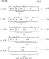
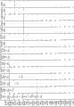
现在参见图12A-12G,说明了用于本发明的优选的实施方案的16位乘法器和40位加法器的实和虚的灵活的数据类型的对齐的图表。在每个图表的每行,在最左边的列说明数据类型,在中间的列说明到SXA、SYA、SXM或SYM数据总线的一个或多个上的输出并且最右边的列说明核心处理器200的信号处理器300A-300D的等价信号处理配置以便执行运算。利用变量N来表示矢量数或操作数被使用的次数的矢量化格式说明了数据类型。当变量N是1时,预计将用一组X和Y操作数执行一个运算。当变量N是2时,预计将在两组X和Y操作数上在一个周期里一起执行两个运算。在任何情况下,两个操作数数据类型需要被规定并且如果不匹配,也就是数据类型不匹配,则需要发生数据类型匹配,这将在下面参考图13A-13C、14和15讨论。Referring now to FIGS. 12A-12G , diagrams illustrating the alignment of real and imaginary flexible data types for the 16-bit multiplier and 40-bit adder of the preferred embodiment of the present invention are shown. In each row of each diagram, the leftmost column illustrates the data type, the middle column illustrates the output to one or more of the SXA, SYA, SXM, or SYM data buses and the rightmost column illustrates the
例如数据类型1 x 4R、1 x 8R、1 x 16R、1 x 32R、2 x 4R、2 x 8R、2 x 16R、1 X 4C、1 x 8C、1 x 16C、1 x 32C、2 x 4C、2 x 8C以及2 x 16C都可以通过被打包成4个或8个16位域越过64位X和/或Y总线被并行加载到信号处理单元。如果X和Y总线的64位都被用于在相同的周期加载两个操作数,则数据类型2 x 32R、1 x 40R以及1 x 40C可以在一个周期中被一起加戴到信号处理单元中。数据类型2 x 32C或者高阶(higher order)需要多个周期来越过64位X和/或Y总线加载操作数。除此之外,32或40位操作数的上半字(也就是16位)可被用于匹配例如16位乘法器。在这种情况下较低的位可作为对运算无意义而被丢弃。半字的其他位宽度可以被提供来匹配给定位宽度的其他硬件组件。利用半字,数据类型2 x 32R、1 x 40R以及1 x 40C允许操作数被加载到更少的信号处理单元并且避免了否则可能需要的进位路径。For example data types 1 x 4R, 1 x 8R, 1 x 16R, 1 x 32R, 2 x 4R, 2 x 8R, 2 x 16R, 1 X 4C, 1 x 8C, 1 x 16C, 1 x 32C, 2 x 4C , 2 x 8C, and 2 x 16C can all be loaded in parallel to the signal processing unit across the 64-bit X and/or Y bus by being packed into 4 or 8 16-bit fields.
现在参见图12A,说明了将数据类型1 x 4R、1 x 8R、1 x 16R、1 x 32R以及1 x 40R对齐到40位加法器中的示例图表。除了40位数据类型1 x 40R之外,在每种情况下的符号位都位于40位数据字的位31并且被耦合到40位加法器。在每种情况下的数据域来自X或Y总线上的存储器或者来自离开不同总线的寄存器。Referring now to FIG. 12A , an example diagram illustrating the alignment of data types 1 x 4R, 1 x 8R, 1 x 16R, 1 x 32R, and 1 x 40R into a 40-bit adder is illustrated. The sign bit in each case is located in
来自X或Y总线的1 x 4R数据类型的四位数据域被对齐到位位置28-31,其符号位在SXA或SYA总线的位31。符号位被包括作为4、8、16或32位字的操作数的最高有效位(MSB)。零被打包或者插入SXA总线或者SYA总线的位0-27的最低有效位(LSB)以便填满。包含扩展符号位31的保护位,被分配给SXA或SYA的位32-39。以这种方式,1 x 4R数据类型被转换为40位字,由信号处理单元300中的40位加法器之一用于加法、减法或最小/最大运算。The four-bit data field of the 1 x 4R data type from the X or Y bus is aligned to bit positions 28-31, with the sign bit in
来自X或Y总线的1 x 8R数据类型的8位数据域被对齐到SXA或SYA的位24-31,在位31是符号位。零被打包或者插入位0-23的LSB。包含扩展符号位31的保护位,被分配到位32-39。以这种方式,1 x 8R数据类型被转换为40位字,由信号处理单元300中的40位加法器之一用于加法、减法或最小/最大运算。The 8-bit data field of the 1 x 8R data type from the X or Y bus is aligned to bits 24-31 of SXA or SYA, where
对于1 x 16R数据类型,来自X或Y总线的16位数据域被对齐到SXA或SYA总线上的位16-31,在位31包括符号位。零被打包或者插入位0-15的LSB而保护位被分配到位32-39。以这种方式,1 x 16R数据类型被转换为40位字,由信号处理单元300中的40位加法器之一用于加法、减法或最小/最大运算。For the 1 x 16R data type, the 16-bit data field from the X or Y bus is aligned to bits 16-31 on the SXA or SYA bus, including the sign bit at
对于1 x 32R数据类型,来自X或Y总线的32位数据域被对齐到位0-31,在位31包括符号位。包含扩展符号位31的保护位被一起打包成位32-39以便使40位字完整。以这种方式,1 x 32R数据类型被转换为40位字,由信号处理单元300中的40位加法器之一用于加法、减法或最小/最大运算。For the 1 x 32R data type, the 32-bit data field from the X or Y bus is aligned to bits 0-31, including the sign bit at
对于1x40R数据类型,来自X或Y总线的所有40位数据域被分配到SXA或SYA总线的位0-39,因此信号处理单元的一个加法器可以每次利用数据域的所有40位执行加法、减法或最小/最大运算。For the 1x40R data type, all 40 bits of the data field from the X or Y bus are allocated to bits 0-39 of the SXA or SYA bus, so one adder of the signal processing unit can use all 40 bits of the data field at a time to perform addition, Subtraction or min/max operations.
如前面所谈论的,多路复用器1101和1104促进了实数数据类型到40位域的转换供信号处理单元里的40位加法器使用。这些多路复用器的每个将数据域转换到包括符号位的合适的位位置并且将零填充到未使用的LSB并且按SXA总线550和SYA总线554所需要的分配保护位。As previously discussed,
现在参见图12B,说明了将数据类型1 x 4R、1 x 8R、1 x 16R、1 x 32R以及1 x 40R对齐到16位字用于16位乘法器的示例图表。对于1 x 4R数据类型,来自X或Y总线的四位数据域的位0-3被分别对齐到SXM或SYM总线的位位置12-15。零被打包或者插入SXA总线或者SYA总线的位0-11的低有效位(LSB)以便填满。以这种方式,1 x 4R数据类型的一个数据采样被转换为16位字,由信号处理单元300中的16位乘法器之一用于乘法或MAC运算。Referring now to FIG. 12B , there is illustrated an example diagram for aligning data types 1 x 4R, 1 x 8R, 1 x 16R, 1 x 32R, and 1 x 40R to 16-bit words for a 16-bit multiplier. For the 1 x 4R data type, bits 0-3 of the four-bit data field from the X or Y bus are aligned to bit positions 12-15 of the SXM or SYM bus, respectively. Zeros are packed or inserted into the least significant bits (LSBs) of bits 0-11 of the SXA bus or SYA bus to fill. In this way, one data sample of the 1 x 4R data type is converted into a 16-bit word, which is used for multiplication or MAC operations by one of the 16-bit multipliers in the
对于1 x 8R数据类型,来自X或Y总线的8位数据域的位0-7分别位于SXM或SYM的位8-15,零被打包到位0-7。以这种方式,1 x 8R数据类型被转换为16位字,由信号处理单元300中的16位乘法器使用。For the 1 x 8R data type, bits 0-7 of the 8-bit data field from the X or Y bus are located in bits 8-15 of SXM or SYM respectively, and zeros are packed into bits 0-7. In this way, the 1 x 8R data type is converted into a 16-bit word, which is used by the 16-bit multiplier in the
对于1 x 16R数据类型,来自X或Y总线的16位数据域的位0-15被对齐到SXM或SYM总线的位0-15里,因此一个信号处理单元可以每次乘以所有的16位。For the 1 x 16R data type, bits 0-15 of the 16-bit data field from the X or Y bus are aligned to bits 0-15 of the SXM or SYM bus, so one signal processing unit can multiply all 16 bits at a time .
对于1 x 32R数据类型,来自X或Y总线的数据域的位0-32被分成两个16位的半字。位16-31被对齐到信号处理单元300的SXM或SYM总线的位0-15。在一个实施方案中,操作数的位0-15的下半字因为无意义所以被丢弃。在这种情况下,一个信号处理单元被利用来处理每个操作数的上半字的信息的16位。在替代实施方案中,位0-15的低半字可以被对齐到另一个信号处理单元300的SXM或SYM总线的位0-15。在这种情况下,两个信号处理单元被利用来为每个半字乘以信息的16位并且低阶信号处理单元有到高阶信号处理单元的进位信号路径以便处理32位数据域。但是,通过利用信号处理单元之间没有进位信号路径的实施方案,减少了处理时间。For the 1 x 32R data type, bits 0-32 of the data field from the X or Y bus are divided into two 16-bit halfwords. Bits 16-31 are aligned to bits 0-15 of the SXM or SYM bus of the
对于1 x 40R数据类型,在一个实施方案中来自X或Y总线的40位数据域的位0-39通过丢弃掉8个最高有效位(MSB)以及16个最低有效位(LSB)被减少到16位半字。在这种情况下,原始操作数的40位的位16-31被选择作为一个信号处理单元的乘法操作数。For the 1 x 40R data type, bits 0-39 of the 40-bit data field from the X or Y bus are reduced to 16-bit halfword. In this case, bits 16-31 of the 40 bits of the original operand are selected as the multiplication operand of one signal processing unit.
如前面所谈论的,多路复用器1102和1106促进了实数数据类型到16位域的转换,供信号处理单元里的16位加法器使用。这些多路复用器的每个将数据域转换到合适的位位置,包括按照SXM总线552A/552B和SYM总线556A/556B所需要的,将零填充到未使用的LSB。多路复用器1102和1106的每个为信号处理单元300A-300D的每个中的各个乘法器执行置换运算、对齐运算以及零插入。As previously discussed,
现在参见12C,说明了为一个或多个40位加法器将复数数据类型1 x 4C、1 x 8C、1 x 16C、1 x 32C以及1 x 40C对齐到一个或多个40位字中的示例图表。See now 12C for an example of aligning complex data types 1 x 4C, 1 x 8C, 1 x 16C, 1 x 32C, and 1 x 40C into one or more 40-bit words for one or more 40-bit adders chart.
对于复数数据类型,至少两个信号处理单元被用于执行实项和虚项的复数计算。对于40位加法器,典型地一个信号处理单元接收复数数据类型操作数的实数部分而另一个信号处理单元接收虚数部分。For complex data types, at least two signal processing units are used to perform complex calculations of real and imaginary terms. For a 40-bit adder, typically one signal processing unit receives the real part of a complex data type operand and the other signal processing unit receives the imaginary part.
对于1 x 4C数据类型,实数域的位0-4被分别对齐到第一个40位字的位28-31,符号位在位位置31。保护位被加到位域32-39而零被插入第一个40位字的位0-27。类似的,虚数域的位0-4被分别对齐到第二个40位字的位28-31,符号位在位位置31。保护位被分配到第二个40位字的位32-39而零被打包到位0-27。以这种方式,1 x 4C复数数据类型被转换成两个40位字作为两个信号处理单元中两个40位加法器的操作数。For the 1 x 4C data type, bits 0-4 of the real number field are aligned to bits 28-31 of the first 40-bit word, respectively, with the sign bit in
对于1 x 8C数据类型,来自X或Y总线的实数域的位0-7被位于在SXA或SYA总线之一上的第一个40位操作数的位位置24-31,符号位在位位置31。保护位被分配到第一个40位操作数的位位置32-39而零被打包到位0-23。来自X或Y总线的复数数据域的位0-7被对齐到在SXA或SYA总线中另一条上的第二个40位字的位24-31,符号位在位位置31。已经被初始化为零的保护位被分配到位32-39而零被打包到第二个40位操作数的位0-23。以这种方式,1 x 8C复数数据类型被转换成两个40位字作为两个信号处理单元中两个40位加法器的操作数。For the 1 x 8C data type, bits 0-7 of the real number field from the X or Y bus are placed in bit positions 24-31 of the first 40-bit operand on one of the SXA or SYA buses, and the sign bit is in
对于1 x 16C数据类型,来自X或Y总线的实数域的位0-16被对齐到在SXA或SYA总线之一上的第一个40位操作数的位位置16-31,符号位在位位置31。保护位被分配到第一个40位操作数的位位置32-39而零被打包到位0-15。类似的,对于SXA或SYA总线中另一条上用于第二个40位操作数来自X或Y总线的虚数数据域的位0-16被对齐到位16-31,包括位31的符号位。保护位被分配到SXA或SYA总线上第二个40位操作数的位32-39而零被打包到位0-15。For the 1 x 16C data type, bits 0-16 of the real field from the X or Y bus are aligned to bit positions 16-31 of the first 40-bit operand on either the SXA or SYA bus, with the sign bit in
对于1 x 32C数据类型,32位实数的位0-31被分别对齐到在SXA或SYA总线之一上的第一个40位操作数的位0-31,符号位被包括在位位置31。保护位被分配到第一个40位操作数的位位置32-39。类似的,虚数数据域的位0-31被对齐到SXA或SYA总线中另一个上的第二个40位操作数的位位置0-31,符号位是位位置31。保护位被插入到第二个40位操作数的位32-39。因此,1 x 32C数据类型被转换成两个40位操作数由两个信号处理单元300的两个40位加法器用于在一个周期里处理虚项和实项两者。For the 1 x 32C data type, bits 0-31 of the 32-bit real number are aligned to bits 0-31 of the first 40-bit operand on one of the SXA or SYA buses, respectively, and the sign bit is included in
对于1 x 40C复数数据类型,来自X或Y总线的实数域的位0-39被对齐到SXA或SYA总线之一上第一个40位操作数的位0-39供一个信号处理单元使用。来自X或Y总线的虚数域的位0-39被对齐到SXA或SYA总线中的另一条上的第二个40位操作数的位位置0-39供第二个信号处理单元使用,因此两个信号处理单元被用于在一个周期里处理两个40位数据域。For a 1 x 40C complex data type, bits 0-39 of the real field from the X or Y bus are aligned to bits 0-39 of the first 40-bit operand on one of the SXA or SYA buses for use by one signal processing unit. Bits 0-39 of the imaginary field from the X or Y bus are aligned to bit positions 0-39 of the second 40-bit operand on the other of the SXA or SYA buses for use by the second signal processing unit, so both A signal processing unit is used to process two 40-bit data fields in one cycle.
现在参见12D,说明了为四个40位加法器将复数数据类型2 x 16C、2 x 32C以及2 x 40C对齐到四个40位字中的示例图表。在这种情况下,具有灵活位宽度的两组操作数(DATA1和DATA2)在相同周期里被引入。See now 12D for an example diagram illustrating the alignment of
对于2 x 16C复数类型,来自X或Y总线的四个16位数据域被对齐到四个40位操作数,每个信号处理单元300A-300D一个。来自X或Y总线的DATA1的实数域的位0-15被分别对齐到对于第一个信号处理单元在SXA或SYA总线之一上的第一个40位操作数的位16-31,包括在位位置31的符号位。来自X或Y总线的DATA1的复数域的位0-15被分别对齐到对于第二个信号处理单元的在SXA或SYA总线中另一条上的第二个40位操作数的位16-31,包括在位位置31的符号位。来自X或Y总线的DATA2的实数域的位0-15被分别对齐到对于第三个信号处理单元在SXA或SYA总线中另一条上的第三个40位操作数的位16-31,包括在位位置31的符号位。来自X或Y总线的DATA2的复数域的位0-15被分别对齐到对于第四个信号处理单元的在SXA或SYA总线中另一条上的第四个40位操作数的位16-31,包括在位位置31的符号位。零被打包到如图12D所示的四个SXA或四个SYA总线上的每个40位操作数中的位置0-15并且保护位被分配到位32-39。因此,2 x 16C复数数据类型被对齐到四个40位操作数由四个信号处理单元中的四个40位加法器使用。For 2 x 16C complex types, four 16-bit data fields from the X or Y bus are aligned to four 40-bit operands, one for each
2 x 32C复数数据类型和2 x 40C复数数据类型类似于2 x 16数据类型被对齐到四个操作数但是有不同的位对齐和零插入或者保护位的分配。这些位对齐和零打包/插入以及保护位的分配如图12D中说明的所示。The 2 x 32C complex data type and the 2 x 40C complex data type are similar to the 2 x 16 data type aligned to four operands but have different bit alignment and assignment of zero insertion or guard bits. These bit alignment and zero packing/insertion and allocation of guard bits are shown as illustrated in Figure 12D.
以这种方式,其中S由加法器的宽度所限制的两个2 x SC复数数据类型,可以被对齐到四个操作数中,供四个信号处理单元300中的四个加法器用于在一个周期中处理复数数据类型。In this way, two 2 x SC complex data types, where S is bounded by the width of the adder, can be aligned into four operands for use by the four adders in the four
现在参见图12E,说明了为一个或多个16位乘法器将复数数据类型1 x 4C、1 x 8C、1 x 16C、1 x 32C以及1 x 40C对齐到一个或多个16位字中的示例图表。Referring now to FIG. 12E , the alignment of the complex data types 1 x 4C, 1 x 8C, 1 x 16C, 1 x 32C, and 1 x 40C into one or more 16-bit words for one or more 16-bit multipliers is illustrated. Example chart.
对于1 x 4C复数数据类型,如图12E所示,来自X或Y总线的实数域的位0-3被分别对齐到SXM或SYM总线之一上的第一个16位操作数的位12-15。来自X或Y总线的虚数域的位0-3被分别对齐到SXM或SYM总线中另一条上的第二个16位操作数的位12-15。第一个和第二个16位操作数的每个的位0-11被用零打包。以这种方式,1x4C复数数据类型的每个复数项被转换成两个16位字作为两个信号处理单元中两个16位乘法器的操作数。1 x 8C数据类型和1 x 16C数据类型如1 x 4C一样被类似地转换为两个16位操作数,但是有如图12E中说明和显示的不同的位对齐。图12E中的复数数据类型1 x 4C、1 x 8C以及1 x 16C利用两个信号处理单元并且将其各个数据位域对齐到两个16位字,供在一个周期中两个信号处理单元中的两个16位乘法器使用。For the 1 x 4C complex data type, as shown in Figure 12E, bits 0-3 of the real field from the X or Y bus are aligned to bits 12-3 of the first 16-bit operand on one of the SXM or SYM buses, respectively. 15. Bits 0-3 of the imaginary field from the X or Y bus are aligned to bits 12-15 of the second 16-bit operand on the other of the SXM or SYM buses, respectively. Bits 0-11 of each of the first and second 16-bit operands are packed with zeros. In this way, each complex term of the 1x4C complex data type is converted into two 16-bit words as operands of two 16-bit multipliers in two signal processing units. The 1 x 8C data type and the 1 x 16C data type are converted similarly to two 16-bit operands as 1 x 4C, but with different bit alignments as illustrated and shown in Figure 12E. The complex data types 1 x 4C, 1 x 8C, and 1 x 16C in Figure 12E utilize two signal processing units and align their respective data bit fields into two 16-bit words for use in two signal processing units in one cycle Two 16-bit multipliers are used.
对于操作数具有位0-31的1 x 32C复数数据类型,在一个实施方案中,每个操作数的实部和虚部的位16-31的上半字被选择并且从总线SXM或SYM复用到两个16位乘法器中,而下半字被丢弃。在替代实施方案中,实部和虚部的上半字和下半字被复用到四个16位乘法器中,用于与从下半字乘法器到上半字乘法器的进位相乘。For 1 x 32C complex data types with operands having bits 0-31, in one embodiment, the upper halfword of bits 16-31 of the real and imaginary parts of each operand is selected and complexed from bus SXM or SYM used in two 16-bit multipliers, and the lower halfword is discarded. In an alternate implementation, the upper and lower halfwords of the real and imaginary parts are multiplexed into four 16-bit multipliers for multiplying with the carry from the lower halfword multiplier to the upper halfword multiplier .
对于操作数具有位0-39的1 x 40C复数数据类型,在一个实施方案中,每个操作数的实部和虚部的位16-31的中间半字被选择并且从总线SXM或SYM复用到两个16位乘法器中,而上面的位32-39以及下半字位0-15被丢弃。在替代实施方案中,为复数数据类型的实部和虚部,该字被多路复用器利用从低位乘法器到高位乘法器的进位从多个乘法器中分离。For 1 x 40C complex data types with operands having bits 0-39, in one embodiment, the middle halfword of bits 16-31 of the real and imaginary parts of each operand is selected and complexed from bus SXM or SYM Two 16-bit multipliers are used, while upper bits 32-39 and lower halfword bits 0-15 are discarded. In an alternative embodiment, the real and imaginary parts of a complex data type, the word is split across multiple multipliers by a multiplexer with a carry from a lower multiplier to an upper multiplier.
现在参见12F,说明了为四个16位乘法器将复数数据类型2 x 32C或2 x 40C以及2 x 16C对齐到四个16位字中的示例图表。See now 12F for an example diagram illustrating the alignment of
对于2 x 32C数据类型,对于第一个信号单元,X或Y总线上第一个操作数的实数(RHWu)的上半字的位0-15被分别对齐到SXM或SYM总线之一上第一个16位操作数的位0-15,并且对于第一个信号单元,X或Y总线上第二个操作数的实数域的上半字的位0-15被分别对齐到SXM或SYM总线中另一条上的第二个16位操作数的位0-15。对于第二个信号单元,X或Y总线上第一个操作数的虚数的上半字(IHWu)的位0-15被对齐到另一条SXM或SYM总线上的第三个16位操作数的位0-15,并且对于第二个信号单元,X或Y总线上第二个操作数的虚数域的上半字的位0-15被分别对齐到SXM或SYM总线中另一条上的第四个16位操作数的位0-15。因此,2x32C复数数据类型使用两个信号处理单元并且将32位实数和虚数域转换为16位操作数,供两个信号处理单元中的16位乘法器使用。For the 2 x 32C data type, for the first signal unit, bits 0-15 of the upper halfword of the real number (RHWu) of the first operand on the X or Y bus are aligned to the first half word on one of the SXM or SYM buses, respectively. Bits 0-15 of a 16-bit operand, and for the first signal unit, bits 0-15 of the upper halfword of the real field of the second operand on the X or Y bus are aligned to the SXM or SYM bus, respectively Bits 0-15 of the second 16-bit operand on the other strip. For the second signal unit, bits 0-15 of the imaginary upper halfword (IHWu) of the first operand on the X or Y bus are aligned to the third 16-bit operand on the other SXM or SYM bus. bits 0-15, and for the second signal unit, bits 0-15 of the upper halfword of the imaginary field of the second operand on the X or Y bus are aligned to the fourth on the other of the SXM or SYM buses, respectively bits 0-15 of a 16-bit operand. Thus, the 2x32C complex data type uses two signal processing units and converts the 32-bit real and imaginary fields into 16-bit operands for the 16-bit multipliers in the two signal processing units.
对于2x16C数据类型,两个复数操作数可以被指定并且作为一个通过64位数据总线复用到两个乘法器。在这种情况下,对于一个信号处理单元,来自X或Y总线的第一个操作数的实数域的位0-15被对齐到在SXM或SYM总线之一上的第一个16位操作数的位0-15,而对于第二个信号处理单元,X或Y总线上的第一个操作数的虚数的位0-15被对齐到在SXM或SYM总线中另一条上的第二个16位操作数的位0-15。对于第一个信号处理单元,X或Y总线上的第二个操作数的实数域的位0-15被对齐到第三个16位操作数的位0-15,并且对于第二个信号处理单元,X或Y总线上的第二个操作数的虚数域的位0-15被对齐到SXM或SYM总线中另一条上的第四个16位操作数的位0-15。因此,2 x 16C数据类型使用四个信号处理单元来在一个周期中处理四个16位乘法器中四个16位操作数的每个。For 2x16C data types, two complex operands can be specified and multiplexed as one to two multipliers over the 64-bit data bus. In this case, for a signal processing unit, bits 0-15 of the real field of the first operand from the X or Y bus are aligned to the first 16-bit operand on one of the SXM or SYM buses bits 0-15 of the first operand on the X or Y bus are aligned to the second 16 on the other of the SXM or SYM buses for the second signal processing unit Bits 0-15 of the bit operand. For the first signal processing unit, bits 0-15 of the real field of the second operand on the X or Y bus are aligned to bits 0-15 of the third 16-bit operand, and for the second signal processing unit, bits 0-15 of the imaginary field of the second operand on the X or Y bus are aligned to bits 0-15 of the fourth 16-bit operand on the other of the SXM or SYM buses. Thus, the 2 x 16C data type uses four signal processing units to process each of the four 16-bit operands in the four 16-bit multipliers in one cycle.
现在参见图13A、13B和13C,说明了用于两个操作数的类型匹配的通用规则,一般的,数据类型匹配指将两个不同数据类型的两个操作数匹配到一起,因此其可以被给定的数字信号处理运算正确地处理。在图13A中,第一个操作数,操作数1,有N1 x S1实数的数据类型并且第二个操作数,操作数2,有N2 x S2实数的数据类型。两个实数数据类型的操作数类型匹配的通用规则是确定并且选择N1或者N2的最大值以及S1或者S2的最大值。替代的,可以确定并且丢弃N1或者N2的最小值以及S1或者S2的最小值来提供操作数类型匹配。操作数类型匹配提供了可以处理操作数的信号处理单元的数量(N1或者N2的最大值)以及两个操作数的位宽(S1或者S2的最大值)的指示。对于不同的操作数类型,信号处理单元的乘法器和加法器被提供两个不同操作数类型的最佳操作数类型匹配,以便获得结果。来自全异操作数上执行的运算的输出结果采用匹配的数据类型形式。Referring now to Figures 13A, 13B and 13C, general rules for type matching of two operands are illustrated. In general, data type matching refers to matching two operands of two different data types together so that they can be The given digital signal processing operation is correctly processed. In FIG. 13A, the first operand,
现在参见图13B,第一个操作数,操作数1以及第二个操作数,操作数2都是复数类型。两个复数类型的操作数的操作数类型匹配的通用规则类似于匹配两个实数数据类型但是导致复数数据类型。复数类型的操作数数据类型匹配是确定并且选择N1或者N2的最大值以及S1或者S2的最大值。Referring now to FIG. 13B, the first operand,
现在参见图13C,第一个操作数,操作数1是实数类型而第二个操作数,操作数2是复数类型。用于实数类型和复数类型的操作数类型匹配的通用规则是选择有复数类型匹配的N1或者N2的最大值以及S1或者S2的最大值。N1或者N2的最大值表示处理实部或虚部所需的信号处理单元的数量,并且S1或者S2的最大值表示要被对齐到信号处理单元的操作数的位宽度。在数据分类器和对准器502的每个实例中的多路复用器1101、1102、1104和1106,响应合适的多路复用器控制信号来执行来自X总线531或Y总线533的操作数1和操作数2之间的数据类型匹配。置换和对齐被各个核心处理器200自动选择以便通过总线多路复用器的控制将两个操作数的数据类型匹配提供到每个信号处理单元中。Referring now to FIG. 13C, the first operand,
除了自动数据类型匹配之外,本发明响应要被执行的运算(ADD、SUB、MULT、DIVIDE等)、功能单元(加法器和乘法器)的数量以及在每个信号处理单元300A-300D中其各个位宽度、两个操作数的自动数据类型匹配的位宽度、以及是否涉及实数或复数数据类型以及是否要执行标量或矢量功能来操作地匹配数据类型。信号处理单元300A-300D的每个有两个乘法器和三个加法器。在本发明的优选实施方案中,每个乘法器是16位宽并且每个加法器是40位宽。在设置标称数据类型并且读取新数据作为新操作数并且重复乘法、加法或者其他类型的信号处理运算之后,相同数据类型的多个操作数可以被简单地处理。In addition to automatic data type matching, the present invention responds to the operations to be performed (ADD, SUB, MULT, DIVIDE, etc.), the number of functional units (adders and multipliers) and other The respective bit widths, bit widths for automatic data type matching of the two operands, and whether real or complex data types are involved and whether scalar or vector functions are to be performed to operationally match the data types. Each of the
现在参见图14、15A和15B,说明了显示本发明提供的数据类型可操作匹配的示例图表。在图14、15A和15B的每个中,第一个操作数的数据类型被沿上面的行指示并且第二个操作数的数据类型被沿最左边的列指示。在每个图中最上边的行和最左边的列之间的矩阵指示由本发明的实施方案提供的可操作匹配。Referring now to Figures 14, 15A and 15B, there are illustrated example diagrams showing operational matching of data types provided by the present invention. In each of Figures 14, 15A, and 15B, the data type of the first operand is indicated along the upper row and the data type of the second operand is indicated along the leftmost column. The matrix between the topmost row and leftmost column in each figure indicates the operational matching provided by embodiments of the present invention.
在图14中,说明了显示用于信号处理单元的乘法器进行的乘法运算的数据类型匹配的示例图表。具有四位和八位数据类型的操作数在图14中没有说明,其被理解为这些数据类型被转换成16位操作数。在图14中,对于其中描述的实施方案空的单元不被允许运算。但是,如果信号处理单元的数量从4扩展并且乘法器的数据位宽度从16位扩展,则对于其他操作数数据类型组合额外的运算可以被执行。在图14的每个完全(completed)的单元中,运算对于矢量运算需要两个周期并且对于实数数据类型标量运算需要三个周期。因为两个值,实数和虚数总是保留作为结果,因此复数操作数与另一个操作数的标量乘法不被执行。每个完全的单元指示用于执行乘法运算的信号处理单元的数量。例如,1 x 16C操作数和1 x 16C操作数的乘法指示利用了四个信号处理单元。在复数乘法的情况下,操作数是(r1+ji1)和(r2+ji2),其中r1和r2是实项并且i1和i2是虚项。复数乘法的结果对于实项是[(r1 x r2)-(i1 x i2)]并且对于虚项是[(r1 x i2)+(r2 x i1)]。因此,四个信号处理单元在相同周期里一起处理圆括号的乘法。实项和虚项的剩余的加法和减法运算则分别在下一个周期中在两个信号处理单元中一起被执行以便获得最终结果。考虑另一个例子,1 x 16R操作数与1 x 32C操作数的乘法。在这种情况下,图14指示利用四个信号处理单元。操作数是r1和(r2+ji2),其中r1和r2是实数并且i2是虚数。运算结果对于结果的实数部分将是[(r1 x r2)]并且对于结果的虚数部分将是[(r1 x i2)]。因为复数操作数是32位宽,实项和虚项被分为半字。因此运算变成对于实部是[(r1 x r2UHW)+(r1 x r2LHW)]以及[(r1 x i2UHW)+(r1 x i2LHW)],其中UHW分别是每个值的上半字并且LHW是下半字。因此,四个信号处理单元的每个在一个周期一起执行圆括号的乘法而项的加法在下一个周期里在两个信号处理单元中被执行。In FIG. 14 , an example graph showing data type matching for multiplication by the multipliers of the signal processing unit is illustrated. Operands with four-bit and eight-bit data types are not illustrated in Figure 14, it being understood that these data types are converted to 16-bit operands. In FIG. 14, empty cells are not allowed to operate for the embodiment described therein. However, if the number of signal processing units is expanded from 4 and the data bit width of the multiplier is expanded from 16 bits, additional operations combined for other operand data types can be performed. In each completed unit of Figure 14, operations require two cycles for vector operations and three cycles for real data type scalar operations. Scalar multiplication of a complex operand with another operand is not performed because two values, real and imaginary, are always retained as the result. Each complete unit indicates the number of signal processing units for performing multiplication operations. For example, a multiplication of 1 x 16C operands and 1 x 16C operands indicates that four signal processing units are utilized. In the case of complex multiplication, the operands are (r1+ji1) and (r2+ji2), where r1 and r2 are real terms and i1 and i2 are imaginary terms. The result of complex multiplication is [(r1 x r2)-(i1 x i2)] for the real term and [(r1 x i2)+(r2 x i1)] for the imaginary term. Therefore, the four signal processing units process the parenthesis multiplication together in the same cycle. The remaining addition and subtraction operations of the real and imaginary terms, respectively, are then performed together in the two signal processing units in the next cycle to obtain the final result. Consider another example, the multiplication of 1 x 16R operands with 1 x 32C operands. In this case, FIG. 14 indicates that four signal processing units are utilized. The operands are r1 and (r2+ji2), where r1 and r2 are real numbers and i2 is an imaginary number. The result of the operation will be [(r1 x r2)] for the real part of the result and [(r1 x i2)] for the imaginary part of the result. Because complex operands are 32 bits wide, real and imaginary terms are split into halfwords. The operation thus becomes [(r1 x r2UHW)+(r1 x r2LHW)] and [(r1 x i2UHW)+(r1 x i2LHW)] for the real part, where UHW is the upper halfword of each value and LHW is Lower half of the word. Therefore, each of the four signal processing units performs the multiplication of the parentheses together in one cycle and the addition of the terms is performed in the two signal processing units in the next cycle.
现在参见图15A,说明了显示用于由信号处理单元的加法器进行的标量加法的数据类型匹配的示例图表。在图15A中没有说明具有4和8位的数据类型的操作数,被理解为这些数据类型被转换为16位操作数。注意因为两个值,实数和虚数,总是导致涉及复数操作数的运算的事实,利用复数操作数没有执行标量加法。在图15A中,对于其中所述的实施方案空的单元不被允许运算。但是,如果信号处理单元的数量从4扩展并且加法器的数据位宽度从40位扩展,则对于其他操作数数据类型组合额外的运算可以被执行。在图15A的每个完全的单元中,如果两个操作数很容易可用,则标量加法运算可以在一个周期里完成。每个完全的单元指示用于执行标量加法运算的信号处理单元的数量。Referring now to FIG. 15A , there is illustrated an example diagram showing data type matching for scalar addition by adders of a signal processing unit. Operands having data types of 4 and 8 bits are not illustrated in FIG. 15A, it being understood that these data types are converted to 16 bit operands. Note that scalar addition is not performed with complex operands because of the fact that two values, real and imaginary, always result in operations involving complex operands. In FIG. 15A, cells that are empty for the embodiment described therein are not allowed to operate. However, if the number of signal processing units is expanded from 4 and the data bit width of the adder is expanded from 40 bits, additional operations combined for other operand data types can be performed. In each complete unit of Fig. 15A, scalar addition can be done in one cycle if both operands are readily available. Each full unit indicates the number of signal processing units used to perform scalar addition operations.
考虑例如1 x 32R操作数和2 x 16R操作数,其中r1是32位宽的第一个操作数并且r2和r3是每个16位宽的第二组操作数。图15A的图表指示利用两个信号处理单元。标量结果是[(r1+r2)+(r1+r3)]。两个信号处理单元利用其两个40位加法器在一个周期里执行圆括号中的加法运算而在两个信号处理单元之一中的第二个加法在第二个周期里合并中间结果。Consider for example 1 x 32R operands and 2 x 16R operands, where r1 is the first operand that is 32 bits wide and r2 and r3 are the second set of operands that are each 16 bits wide. The graph of Figure 15A indicates the use of two signal processing units. The scalar result is [(r1+r2)+(r1+r3)]. The two signal processing units perform the parenthesized addition in one cycle with their two 40-bit adders and the second addition in one of the two signal processing units combines the intermediate results in a second cycle.
现在参见图15B,说明了显示用于由信号处理单元的加法器进行的矢量加法的数据类型匹配的示例图表。在图15B中没有说明具有4和8位数据类型的操作数,被理解为这些数据类型被转换为16位操作数。在图15B中,对于其中所述的实施方案,空的单元不被允许运算。但是,如果信号处理单元的数量从4扩展并且加法器的数据位宽度从40位扩展,则对于其他操作数数据类型组合,额外的运算可以被执行。在图15B的每个完全的单元中,如果两个操作数很容易可用,则矢量加法运算可以在一个周期里完成。每个完全的单元指示用于执行矢量加法运算的信号处理单元的数量。具有复数数据类型的操作数可被用于执行矢量加法。Referring now to FIG. 15B , there is illustrated an example diagram showing data type matching for vector addition by the adders of the signal processing unit. Operands having 4 and 8 bit data types are not illustrated in Figure 15B, it being understood that these data types are converted to 16 bit operands. In Figure 15B, for the implementation described therein, empty cells are not allowed to operate. However, if the number of signal processing units is expanded from 4 and the data bit width of the adder is expanded from 40 bits, additional operations can be performed for other operand data type combinations. In each complete unit of Fig. 15B, the vector addition operation can be performed in one cycle if both operands are readily available. Each full unit indicates the number of signal processing units used to perform vector addition operations. Operands with complex data types can be used to perform vector addition.
考虑例如1 x 16R操作数和1 x 32C操作数,其中r1是16位宽的第一个操作数并且r2和i2是每个32位宽的第二操作数。图15B的图表指示利用两个信号处理单元。实数1 x 16R操作数被转换成具有零虚部的1 x 16C复操作数。在一个信号处理单元中,实部被加在一起执行(r1+r2),而在另一个信号处理单元中,虚部i2被加到0执行(0+i2)。矢量结果是[(r1+r2)]作为实部并且i2作为虚部。信号处理单元利用40位加法器执行圆括号中的加法运算。Consider for example 1 x 16R operands and 1 x 32C operands, where r1 is the
考虑另一个例子1 x 16C操作数和1 x 32C操作数,对于1 x 16C操作数r1和i1分别是第一个操作数的实部和虚部,每个是16位宽并且r2和i2是第二个操作数的实项和虚项,每个是32位宽。图15B的图表指示利用两个信号处理单元。矢量结果是[(r1+r2)]作为实部并且[(i1+i2)]作为虚部。两个信号处理单元利用40位加法器执行圆括号中的加法运算。Consider another example of 1 x 16C operands and 1 x 32C operands, for 1 x 16C operands r1 and i1 are the real and imaginary parts of the first operand respectively, each is 16 bits wide and r2 and i2 are The real and imaginary terms of the second operand, each 32 bits wide. The graph of Figure 15B indicates the utilization of two signal processing units. The vector result is [(r1+r2)] as the real part and [(i1+i2)] as the imaginary part. The two signal processing units perform the addition in parentheses using 40-bit adders.
现在参见图16,框图说明对于每个信号处理单元的每个数据分类器和对准器里包括的总线多路复用器的控制信号生成。为每个数据分类器和对准器的每个总线多路复用器提供的控制信号提供选择性控制来执行自动数据分类和对齐以及用户选择的置换。对于每个数据分类器和对准器中的X总线,总线多路复用器的多路复用器1101和1102的控制信号将选择用于一个操作数到每个信号处理单元中的数据类型和对齐。对于每个数据分类器和对准器中的Y总线,总线多路复用器的多路复用器1104和1106的控制信号将选择用于第二个操作数到每个信号处理单元中的数据类型和对齐。响应对与来自控制寄存器或指令本身的每个操作数相关的数据类型域解码,通过每个信号处理器中的总线多路复用器的控制提供自动数据类型匹配。来自每个信号处理单元的每个总线多路复用器的结果操作数输出如图5B所示被耦合到每个信号处理单元中的乘法器504A的多路复用器514A、加法器510A的多路复用器520A、以及加法器510B的多路复用器520B。Referring now to FIG. 16, a block diagram illustrates the generation of control signals for the bus multiplexers included in each data sorter and aligner of each signal processing unit. Control signals provided to each bus multiplexer of each data sorter and aligner provide selective control to perform automatic data sorting and alignment as well as user-selected permutations. For each data sorter and aligner in the X bus, the bus multiplexer's control signals to
在图16中,一个或多个DSP指令1600被耦合到指令预解码器1602中。指令预解码器1602可包括一个或多个控制寄存器(“CR”)1604,其包括数据类型域和置换域以便通知预解码器1602操作数的数据类型以及其如何被读到每个信号处理单元中(SP0 300A、SP1 300B、SP2 300C和SP3 300D)。直接或间接地通过一个或多个控制寄存器1604A的一个或多个DSP指令1600,指示两个数据类型域中两个操作数的每个数据类型以及两个置换域中数据总线的任何置换。指令预解码器1602通过为每个操作数比较两个数据类型自动确定最佳数据类型匹配。指令预解码器1602还读取每个操作数的置换域。响应每个操作数的置换域和数据类型,指令预解码器1602生成预解码的控制信号1606用于数据分类多路复用控制。预解码的控制信号1606因此用于每个信号处理单元300中的每个数据分类器和对准器502(数据分类器和对准器502A、502B、502C和502D)中的总线多路复用器1001和1002的控制。这些预解码的控制信号被耦合到每个信号处理单元的最终解码器1610A中,以便为每个信号处理单元300中的每个数据分类器和对准器502的每个总线多路复用器1001和1002分别生成多路复用器控制信号1011和1012。指令预解码器1602还为每个信号处理单元300的其他多路复用器1620B、1620C到1620N生成预解码的控制信号。最终解码器1610B、1610C到1610N接收预解码控制信号来为每个信号处理单元300的每个多路复用器1620B、1620C到1620N生成多路复用器控制信号。以这种方式,X总线和Y总线上的操作数可以被对齐、匹配、置换和选择用于执行数字信号处理运算。In FIG. 16 , one or
如本领域的技术人员所认识到的,本发明有许多优点。本发明的一个优点是用于不同数字信号处理应用的各种数据类型的操作数可以在本发明的应用专用信号处理器中被处理。本发明的另一个优点是提供了自动数据类型匹配。本发明的另一个优点是通过使用指令或控制寄存器中的置换域,操作数可以被自动置换,因此不需要额外的指令来执行到信号处理器的想要的置换。本发明的另一个优点是信号处理单元的数据类型功能可以通过增加额外的信号处理单元被容易地扩展。The present invention has many advantages, as will be appreciated by those skilled in the art. An advantage of the invention is that operands of various data types for different digital signal processing applications can be processed in the application-specific signal processor of the invention. Another advantage of the present invention is that it provides automatic data type matching. Another advantage of the present invention is that by using the permutation fields in the instruction or control registers, operands can be permuted automatically, so no additional instructions are required to perform the desired permutation to the signal processor. Another advantage of the invention is that the data type functionality of the signal processing unit can be easily extended by adding additional signal processing units.
因此描述了本发明的优选实施方案。虽然在附图中已经描述和显示了本发明的某些示例实施方案,应该理解这些实施方案对于本发明上仅是说明性的并且不是限制性的,并且本发明不限于显示和描述的特定的结构和方案,因为对于本领域的普通技术人员可以有各种其他的修改。例如,数据分类和对齐的本发明已经参考用于从存储器访问操作数的存储器访问寄存器被描述,但是操作数可以从寄存器被访问并且还可以通过本发明被适当地数据分类和对齐。虽然在本发明的优选实施方案中利用了16位乘法器,具有更大位宽的乘法器也可以被利用并且提供更大的数据类型灵活性。除此之外,数据存储器和信号处理单元之间的数据总线的大小可以从例如64位增加到80位并且提供更大的数据类型灵活性。而且,可以提供额外的信号处理单元因此也可以满足更大位宽的操作数或更大量的操作数在一个周期中一起处理。Preferred embodiments of the invention have thus been described. While certain exemplary embodiments of the present invention have been described and shown in the drawings, it should be understood that these embodiments are illustrative only and not restrictive of the invention, and that the invention is not limited to the specific ones shown and described. structures and schemes, as various other modifications may occur to those skilled in the art. For example, the invention of data sorting and alignment has been described with reference to memory access registers for accessing operands from memory, but operands can be accessed from registers and also be properly data sorted and aligned by the invention. Although 16-bit multipliers are utilized in the preferred embodiment of the present invention, multipliers with larger bit widths can also be utilized and provide greater data type flexibility. In addition to this, the size of the data bus between the data memory and the signal processing unit can be increased from eg 64 bits to 80 bits and provides greater data type flexibility. Moreover, additional signal processing units can be provided so that operands with a larger bit width or a larger number of operands can be processed together in one cycle.
除此之外,本发明可以被在硬件、软件、固件或其组合中实现并且在系统、子系统、组件或其子组件中被利用。当在软件中实现时,本发明的元件基本上是用于执行必要的任务的代码段。程序或代码段可被存储在处理器可读介质中或者被传输介质或通信链路上的载波中具体化的计算机数据信号发送。“处理器可读介质”可包括可以存储或发送信息的任何介质。处理器可读介质的例子包括电路、半导体存储器设备、ROM、闪存、可擦除ROM(EROM)、软盘、CD-ROM、光盘、硬盘、光纤介质、射频(RF)链路等。计算机数据信号包括可以在如电子网络信道、光纤、空气、电磁、RF链路等传输介质上传播的任何信号。代码段可以通过如互联网、内联网等的计算机网下载。在任何情况下,本发明不应该被解释为由这些实施方案所限制,而应该根据所附权利要求被解释。Among other things, the invention can be implemented in hardware, software, firmware or a combination thereof and utilized in a system, subsystem, component or subcomponent thereof. When implemented in software, the elements of the invention are basically the code segments to perform the necessary tasks. Programs or code segments may be stored in a processor readable medium or transmitted in a computer data signal embodied in a carrier wave over a transmission medium or communication link. A "processor-readable medium" may include any medium that can store or transmit information. Examples of processor-readable media include circuits, semiconductor memory devices, ROM, flash memory, erasable ROM (EROM), floppy disks, CD-ROMs, optical disks, hard disks, fiber optic media, radio frequency (RF) links, and the like. Computer data signals include any signal that can travel over a transmission medium such as an electronic network channel, fiber optics, air, electromagnetic, RF links, or the like. The code segments may be downloaded via a computer network such as the Internet, an intranet, or the like. In any event, the invention should not be construed as limited by the embodiments, but rather should be construed in accordance with the appended claims.
Claims (32)
Applications Claiming Priority (2)
| Application Number | Priority Date | Filing Date | Title |
|---|---|---|---|
| US09/652,556US6557096B1 (en) | 1999-10-25 | 2000-08-31 | Processors with data typer and aligner selectively coupling data bits of data buses to adder and multiplier functional blocks to execute instructions with flexible data types |
| US09/652,556 | 2000-08-31 |
Related Child Applications (3)
| Application Number | Title | Priority Date | Filing Date |
|---|---|---|---|
| CN200710138162.1ADivisionCN100555215C (en) | 2000-08-31 | 2001-08-16 | The equipment that is used for flexible data types |
| CN200710138160.2ADivisionCN101101540B (en) | 2000-08-31 | 2001-08-16 | Method for flexible data types |
| CN200710138161.7ADivisionCN100555214C (en) | 2000-08-31 | 2001-08-16 | The method that is used for flexible data types |
Publications (2)
| Publication Number | Publication Date |
|---|---|
| CN1568455A CN1568455A (en) | 2005-01-19 |
| CN100520707Ctrue CN100520707C (en) | 2009-07-29 |
Family
ID=24617256
Family Applications (4)
| Application Number | Title | Priority Date | Filing Date |
|---|---|---|---|
| CN200710138160.2AExpired - Fee RelatedCN101101540B (en) | 2000-08-31 | 2001-08-16 | Method for flexible data types |
| CN200710138161.7AExpired - Fee RelatedCN100555214C (en) | 2000-08-31 | 2001-08-16 | The method that is used for flexible data types |
| CN200710138162.1AExpired - Fee RelatedCN100555215C (en) | 2000-08-31 | 2001-08-16 | The equipment that is used for flexible data types |
| CN01817951.7AExpired - Fee RelatedCN100520707C (en) | 2000-08-31 | 2001-08-16 | Method and apparatus for flexible data types |
Family Applications Before (3)
| Application Number | Title | Priority Date | Filing Date |
|---|---|---|---|
| CN200710138160.2AExpired - Fee RelatedCN101101540B (en) | 2000-08-31 | 2001-08-16 | Method for flexible data types |
| CN200710138161.7AExpired - Fee RelatedCN100555214C (en) | 2000-08-31 | 2001-08-16 | The method that is used for flexible data types |
| CN200710138162.1AExpired - Fee RelatedCN100555215C (en) | 2000-08-31 | 2001-08-16 | The equipment that is used for flexible data types |
Country Status (7)
| Country | Link |
|---|---|
| US (3) | US6557096B1 (en) |
| EP (1) | EP1323026B1 (en) |
| CN (4) | CN101101540B (en) |
| AT (1) | ATE323904T1 (en) |
| AU (1) | AU2001283408A1 (en) |
| DE (1) | DE60118945T2 (en) |
| WO (1) | WO2002019093A1 (en) |
Families Citing this family (74)
| Publication number | Priority date | Publication date | Assignee | Title |
|---|---|---|---|---|
| US6557096B1 (en)* | 1999-10-25 | 2003-04-29 | Intel Corporation | Processors with data typer and aligner selectively coupling data bits of data buses to adder and multiplier functional blocks to execute instructions with flexible data types |
| US20020078342A1 (en)* | 2000-09-25 | 2002-06-20 | Broadcom Corporation | E-commerce security processor alignment logic |
| US20020061107A1 (en)* | 2000-09-25 | 2002-05-23 | Tham Terry K. | Methods and apparatus for implementing a cryptography engine |
| US6813734B1 (en)* | 2001-01-26 | 2004-11-02 | Catamaran Communications Incorporated | Method and apparatus for data alignment |
| US20030039256A1 (en)* | 2001-08-24 | 2003-02-27 | Klas Carlberg | Distribution of connection handling in a processor cluster |
| US6965985B2 (en)* | 2001-11-27 | 2005-11-15 | Sun Mirosystems, Inc. | Sign generation bypass path to aligner for reducing signed data load latency |
| US6961888B2 (en)* | 2002-08-20 | 2005-11-01 | Flarion Technologies, Inc. | Methods and apparatus for encoding LDPC codes |
| US7185177B2 (en)* | 2002-08-26 | 2007-02-27 | Gerald George Pechanek | Methods and apparatus for meta-architecture defined programmable instruction fetch functions supporting assembled variable length instruction processors |
| US7320013B2 (en)* | 2002-12-12 | 2008-01-15 | Adaptec, Inc. | Method and apparatus for aligning operands for a processor |
| US20050055544A1 (en)* | 2003-07-30 | 2005-03-10 | International Business Machines Corporation | Central processing unit having a module for processing of function calls |
| US20050071610A1 (en)* | 2003-09-30 | 2005-03-31 | International Business Machines Corporation | Method and apparatus for debug support for individual instructions and memory locations |
| US20050071612A1 (en)* | 2003-09-30 | 2005-03-31 | International Business Machines Corporation | Method and apparatus for generating interrupts upon execution of marked instructions and upon access to marked memory locations |
| US7395527B2 (en)* | 2003-09-30 | 2008-07-01 | International Business Machines Corporation | Method and apparatus for counting instruction execution and data accesses |
| US20050071609A1 (en)* | 2003-09-30 | 2005-03-31 | International Business Machines Corporation | Method and apparatus to autonomically take an exception on specified instructions |
| US20050071816A1 (en)* | 2003-09-30 | 2005-03-31 | International Business Machines Corporation | Method and apparatus to autonomically count instruction execution for applications |
| US7937691B2 (en)* | 2003-09-30 | 2011-05-03 | International Business Machines Corporation | Method and apparatus for counting execution of specific instructions and accesses to specific data locations |
| US20050071611A1 (en)* | 2003-09-30 | 2005-03-31 | International Business Machines Corporation | Method and apparatus for counting data accesses and instruction executions that exceed a threshold |
| US20050071516A1 (en)* | 2003-09-30 | 2005-03-31 | International Business Machines Corporation | Method and apparatus to autonomically profile applications |
| US7373637B2 (en)* | 2003-09-30 | 2008-05-13 | International Business Machines Corporation | Method and apparatus for counting instruction and memory location ranges |
| US20050071821A1 (en)* | 2003-09-30 | 2005-03-31 | International Business Machines Corporation | Method and apparatus to autonomically select instructions for selective counting |
| US9465611B2 (en)* | 2003-10-02 | 2016-10-11 | Broadcom Corporation | Processor execution unit with configurable SIMD functional blocks for complex number operations |
| US7421681B2 (en)* | 2003-10-09 | 2008-09-02 | International Business Machines Corporation | Method and system for autonomic monitoring of semaphore operation in an application |
| US8381037B2 (en)* | 2003-10-09 | 2013-02-19 | International Business Machines Corporation | Method and system for autonomic execution path selection in an application |
| US7415705B2 (en)* | 2004-01-14 | 2008-08-19 | International Business Machines Corporation | Autonomic method and apparatus for hardware assist for patching code |
| US7526757B2 (en)* | 2004-01-14 | 2009-04-28 | International Business Machines Corporation | Method and apparatus for maintaining performance monitoring structures in a page table for use in monitoring performance of a computer program |
| US7895382B2 (en)* | 2004-01-14 | 2011-02-22 | International Business Machines Corporation | Method and apparatus for qualifying collection of performance monitoring events by types of interrupt when interrupt occurs |
| US7197586B2 (en)* | 2004-01-14 | 2007-03-27 | International Business Machines Corporation | Method and system for recording events of an interrupt using pre-interrupt handler and post-interrupt handler |
| US7114036B2 (en)* | 2004-01-14 | 2006-09-26 | International Business Machines Corporation | Method and apparatus for autonomically moving cache entries to dedicated storage when false cache line sharing is detected |
| US7496908B2 (en)* | 2004-01-14 | 2009-02-24 | International Business Machines Corporation | Method and apparatus for optimizing code execution using annotated trace information having performance indicator and counter information |
| US7392370B2 (en) | 2004-01-14 | 2008-06-24 | International Business Machines Corporation | Method and apparatus for autonomically initiating measurement of secondary metrics based on hardware counter values for primary metrics |
| CN100353702C (en)* | 2004-01-20 | 2007-12-05 | 海信集团有限公司 | Method for designing reconfigurable substitution module of reconfigurable cipher code coprocessor |
| US7987453B2 (en)* | 2004-03-18 | 2011-07-26 | International Business Machines Corporation | Method and apparatus for determining computer program flows autonomically using hardware assisted thread stack tracking and cataloged symbolic data |
| US7421684B2 (en) | 2004-03-22 | 2008-09-02 | International Business Machines Corporation | Method and apparatus for autonomic test case feedback using hardware assistance for data coverage |
| US7386690B2 (en)* | 2004-04-29 | 2008-06-10 | International Business Machines Corporation | Method and apparatus for hardware awareness of data types |
| US20050251706A1 (en)* | 2004-04-29 | 2005-11-10 | International Business Machines Corporation | Method and apparatus for data-aware hardware operations |
| US7895473B2 (en)* | 2004-04-29 | 2011-02-22 | International Business Machines Corporation | Method and apparatus for identifying access states for variables |
| US7269718B2 (en)* | 2004-04-29 | 2007-09-11 | International Business Machines Corporation | Method and apparatus for verifying data types to be used for instructions and casting data types if needed |
| US7328374B2 (en)* | 2004-04-29 | 2008-02-05 | International Business Machines Corporation | Method and apparatus for implementing assertions in hardware |
| US7167968B2 (en)* | 2004-04-29 | 2007-01-23 | International Business Machines Corporation | Storage pre-alignment and EBCDIC, ASCII and unicode basic latin conversions for packed decimal data |
| EP1831782A2 (en)* | 2004-07-12 | 2007-09-12 | Halil Kilic | Digital processor and method of processing digital data |
| GB2417105B (en)* | 2004-08-13 | 2008-04-09 | Clearspeed Technology Plc | Processor memory system |
| US7933405B2 (en)* | 2005-04-08 | 2011-04-26 | Icera Inc. | Data access and permute unit |
| US7415595B2 (en)* | 2005-05-24 | 2008-08-19 | Coresonic Ab | Data processing without processor core intervention by chain of accelerators selectively coupled by programmable interconnect network and to memory |
| US7299342B2 (en)* | 2005-05-24 | 2007-11-20 | Coresonic Ab | Complex vector executing clustered SIMD micro-architecture DSP with accelerator coupled complex ALU paths each further including short multiplier/accumulator using two's complement |
| US20070198815A1 (en)* | 2005-08-11 | 2007-08-23 | Coresonic Ab | Programmable digital signal processor having a clustered SIMD microarchitecture including a complex short multiplier and an independent vector load unit |
| WO2007085914A1 (en)* | 2006-01-27 | 2007-08-02 | Freescale Semiconductor, Inc. | Device and method for adding and subtracting two variables and a constant |
| TW200808067A (en)* | 2006-07-31 | 2008-02-01 | Univ Nat Cheng Kung | Prediction module |
| US20080079712A1 (en)* | 2006-09-28 | 2008-04-03 | Eric Oliver Mejdrich | Dual Independent and Shared Resource Vector Execution Units With Shared Register File |
| JP5079342B2 (en) | 2007-01-22 | 2012-11-21 | ルネサスエレクトロニクス株式会社 | Multiprocessor device |
| US7890320B2 (en)* | 2007-04-17 | 2011-02-15 | Microsoft Corporation | Tower of numeric types |
| US8761188B1 (en)* | 2007-05-01 | 2014-06-24 | Altera Corporation | Multi-threaded software-programmable framework for high-performance scalable and modular datapath designs |
| JP5095273B2 (en)* | 2007-06-22 | 2012-12-12 | 株式会社東芝 | Control device |
| US7673120B2 (en)* | 2007-06-27 | 2010-03-02 | Texas Instruments Incorporated | Inter-cluster communication network and heirarchical register files for clustered VLIW processors |
| US20090106526A1 (en)* | 2007-10-22 | 2009-04-23 | David Arnold Luick | Scalar Float Register Overlay on Vector Register File for Efficient Register Allocation and Scalar Float and Vector Register Sharing |
| US8169439B2 (en)* | 2007-10-23 | 2012-05-01 | International Business Machines Corporation | Scalar precision float implementation on the “W” lane of vector unit |
| US8392489B2 (en)* | 2008-02-15 | 2013-03-05 | International Business Machines Corporation | ASCII to binary floating point conversion of decimal real numbers on a vector processor |
| US8060729B1 (en) | 2008-10-03 | 2011-11-15 | Altera Corporation | Software based data flows addressing hardware block based processing requirements |
| US8805916B2 (en)* | 2009-03-03 | 2014-08-12 | Altera Corporation | Digital signal processing circuitry with redundancy and bidirectional data paths |
| US20120278591A1 (en)* | 2011-04-27 | 2012-11-01 | Advanced Micro Devices, Inc. | Crossbar switch module having data movement instruction processor module and methods for implementing the same |
| WO2013101132A1 (en) | 2011-12-29 | 2013-07-04 | Intel Corporation | Processors having fully-connected interconnects shared by vector conflict instructions and permute instructions |
| US9471537B2 (en) | 2013-03-14 | 2016-10-18 | Altera Corporation | Hybrid programmable many-core device with on-chip interconnect |
| US9471388B2 (en) | 2013-03-14 | 2016-10-18 | Altera Corporation | Mapping network applications to a hybrid programmable many-core device |
| US9645820B2 (en) | 2013-06-27 | 2017-05-09 | Intel Corporation | Apparatus and method to reserve and permute bits in a mask register |
| JP5710726B2 (en)* | 2013-10-09 | 2015-04-30 | ファナック株式会社 | Control device for executing control program including floating point arithmetic instruction for controlling machine |
| KR20160061701A (en)* | 2014-11-24 | 2016-06-01 | 삼성전자주식회사 | Method and apparatus for processing data using calculators which have different degree of accuracy respectively |
| CN106650923B (en)* | 2015-10-08 | 2019-04-09 | 上海兆芯集成电路有限公司 | Neural Network Unit with Neural Memory and Neural Processing Unit and Sequencer |
| US10467324B2 (en)* | 2017-05-24 | 2019-11-05 | Microsoft Technology Licensing, Llc | Data packing techniques for hard-wired multiplier circuits |
| KR102343652B1 (en)* | 2017-05-25 | 2021-12-24 | 삼성전자주식회사 | Method for aligning sequence for vector processor |
| US11036499B2 (en)* | 2017-06-30 | 2021-06-15 | Intel Corporation | Systems, apparatuses, and methods for controllable sine and/or cosine operations |
| US11620130B2 (en)* | 2018-02-13 | 2023-04-04 | Shanghai Cambricon Information Technology Co., Ltd | Computing device and method |
| US11609760B2 (en)* | 2018-02-13 | 2023-03-21 | Shanghai Cambricon Information Technology Co., Ltd | Computing device and method |
| CN112068799B (en)* | 2019-06-11 | 2022-08-02 | 云南大学 | Optimal signed binary system fast calculation method and elliptic curve scalar multiplication |
| JP2021124849A (en)* | 2020-02-04 | 2021-08-30 | 富士通株式会社 | Arithmetic processing unit, control method of arithmetic processing unit and arithmetic processing program |
| CN113298843B (en) | 2020-02-24 | 2024-05-14 | 中科寒武纪科技股份有限公司 | Data quantization processing method, device, electronic device and storage medium |
Citations (5)
| Publication number | Priority date | Publication date | Assignee | Title |
|---|---|---|---|---|
| US4068299A (en)* | 1973-12-13 | 1978-01-10 | Honeywell Information Systems, Inc. | Data processing system incorporating a logical compare instruction |
| US5023826A (en)* | 1990-01-11 | 1991-06-11 | Bull Hn Information Systems Inc. | Apparatus for skipping arithmetic calculations involving leading zeros |
| WO1997039404A1 (en)* | 1996-04-17 | 1997-10-23 | Advanced Micro Devices, Inc. | An execute unit configured to selectably interpret an operand as multiple operands or as a single operand |
| GB2317467A (en)* | 1996-09-23 | 1998-03-25 | Advanced Risc Mach Ltd | Input operand control in data processing systems |
| US5887183A (en)* | 1995-01-04 | 1999-03-23 | International Business Machines Corporation | Method and system in a data processing system for loading and storing vectors in a plurality of modes |
Family Cites Families (50)
| Publication number | Priority date | Publication date | Assignee | Title |
|---|---|---|---|---|
| US3930232A (en)* | 1973-11-23 | 1975-12-30 | Raytheon Co | Format insensitive digital computer |
| US4107773A (en) | 1974-05-13 | 1978-08-15 | Texas Instruments Incorporated | Advanced array transform processor with fixed/floating point formats |
| US4219874A (en) | 1978-03-17 | 1980-08-26 | Gusev Valery | Data processing device for variable length multibyte data fields |
| JPS5743239A (en) | 1980-08-27 | 1982-03-11 | Hitachi Ltd | Data processor |
| JPS62175866A (en) | 1986-01-30 | 1987-08-01 | Nec Corp | Signal processor |
| US5142677A (en) | 1989-05-04 | 1992-08-25 | Texas Instruments Incorporated | Context switching devices, systems and methods |
| CA1311063C (en) | 1988-12-16 | 1992-12-01 | Tokumichi Murakami | Digital signal processor |
| US4969118A (en) | 1989-01-13 | 1990-11-06 | International Business Machines Corporation | Floating point unit for calculating A=XY+Z having simultaneous multiply and add |
| US5341374A (en) | 1991-03-01 | 1994-08-23 | Trilan Systems Corporation | Communication network integrating voice data and video with distributed call processing |
| US5241492A (en) | 1991-05-06 | 1993-08-31 | Motorola, Inc. | Apparatus for performing multiply and accumulate instructions with reduced power and a method therefor |
| DE69228980T2 (en)* | 1991-12-06 | 1999-12-02 | National Semiconductor Corp., Santa Clara | Integrated data processing system with CPU core and independent parallel, digital signal processor module |
| US5268855A (en)* | 1992-09-14 | 1993-12-07 | Hewlett-Packard Company | Common format for encoding both single and double precision floating point numbers |
| JPH06150023A (en) | 1992-11-06 | 1994-05-31 | Hitachi Ltd | Microcomputer and system thereof |
| US5452289A (en) | 1993-01-08 | 1995-09-19 | Multi-Tech Systems, Inc. | Computer-based multifunction personal communications system |
| US6154828A (en) | 1993-06-03 | 2000-11-28 | Compaq Computer Corporation | Method and apparatus for employing a cycle bit parallel executing instructions |
| JP3532975B2 (en) | 1993-09-27 | 2004-05-31 | 株式会社ルネサステクノロジ | Microcomputer and method of executing instructions using the same |
| US5574927A (en) | 1994-03-25 | 1996-11-12 | International Meta Systems, Inc. | RISC architecture computer configured for emulation of the instruction set of a target computer |
| US5499272A (en) | 1994-05-31 | 1996-03-12 | Ericsson Ge Mobile Communications Inc. | Diversity receiver for signals with multipath time dispersion |
| US5541917A (en) | 1994-09-12 | 1996-07-30 | Bell Atlantic | Video and TELCO network control functionality |
| JP3579843B2 (en) | 1994-10-24 | 2004-10-20 | 日本テキサス・インスツルメンツ株式会社 | Digital signal processor |
| US5530663A (en) | 1994-11-14 | 1996-06-25 | International Business Machines Corporation | Floating point unit for calculating a compound instruction A+B×C in two cycles |
| DE69529999D1 (en) | 1994-12-08 | 2003-04-24 | Intel Corp | METHOD AND DEVICE ENABLING A PROCESSOR TO ACCESS AN EXTERNAL COMPONENT THROUGH A PRIVATE BUS OR A DISTRIBUTED BUS |
| US5727194A (en) | 1995-06-07 | 1998-03-10 | Hitachi America, Ltd. | Repeat-bit based, compact system and method for implementing zero-overhead loops |
| JP2931890B2 (en) | 1995-07-12 | 1999-08-09 | 三菱電機株式会社 | Data processing device |
| US6295599B1 (en)* | 1995-08-16 | 2001-09-25 | Microunity Systems Engineering | System and method for providing a wide operand architecture |
| US6058408A (en) | 1995-09-05 | 2000-05-02 | Intel Corporation | Method and apparatus for multiplying and accumulating complex numbers in a digital filter |
| US5983253A (en) | 1995-09-05 | 1999-11-09 | Intel Corporation | Computer system for performing complex digital filters |
| US5936872A (en) | 1995-09-05 | 1999-08-10 | Intel Corporation | Method and apparatus for storing complex numbers to allow for efficient complex multiplication operations and performing such complex multiplication operations |
| US5825658A (en) | 1995-09-14 | 1998-10-20 | Vlsi Technology, Inc. | Method and a system for specifying and automatically analyzing multiple clock timing constraints in a VLSI circuit |
| JP3767930B2 (en) | 1995-11-13 | 2006-04-19 | 沖電気工業株式会社 | Information recording / reproducing method and information storage device |
| US5826072A (en) | 1995-11-13 | 1998-10-20 | Oasis Design, Inc. | Pipelined digital signal processor and signal processing system employing same |
| US5881060A (en) | 1996-05-30 | 1999-03-09 | Northern Telecom Limited | Integrated cellular voice and digital packet data telecommunications systems and methods for their operation |
| JP3658072B2 (en) | 1996-02-07 | 2005-06-08 | 株式会社ルネサステクノロジ | Data processing apparatus and data processing method |
| US5673272A (en)* | 1996-02-13 | 1997-09-30 | Teradyne, Inc. | Apparatus and method for performing digital signal processing in an electronic circuit tester |
| US5940785A (en) | 1996-04-29 | 1999-08-17 | International Business Machines Corporation | Performance-temperature optimization by cooperatively varying the voltage and frequency of a circuit |
| DE19625569A1 (en) | 1996-06-26 | 1998-01-02 | Philips Patentverwaltung | Signal processor |
| WO1998006030A1 (en) | 1996-08-07 | 1998-02-12 | Sun Microsystems | Multifunctional execution unit |
| KR100201776B1 (en) | 1996-11-06 | 1999-06-15 | 김영환 | Adaptive equalizer with ring structure |
| US5880984A (en) | 1997-01-13 | 1999-03-09 | International Business Machines Corporation | Method and apparatus for performing high-precision multiply-add calculations using independent multiply and add instruments |
| US6029267A (en) | 1997-11-25 | 2000-02-22 | Lucent Technologies Inc. | Single-cycle, soft decision, compare-select operation using dual-add processor |
| US6185671B1 (en)* | 1998-03-31 | 2001-02-06 | Intel Corporation | Checking data type of operands specified by an instruction using attributes in a tagged array architecture |
| US5995122A (en) | 1998-04-30 | 1999-11-30 | Intel Corporation | Method and apparatus for parallel conversion of color values from a single precision floating point format to an integer format |
| US6178500B1 (en)* | 1998-06-25 | 2001-01-23 | International Business Machines Corporation | Vector packing and saturation detection in the vector permute unit |
| US6209012B1 (en) | 1998-09-02 | 2001-03-27 | Lucent Technologies Inc. | System and method using mode bits to support multiple coding standards |
| JP3123047B2 (en)* | 1998-10-02 | 2001-01-09 | 日本電気株式会社 | Microprocessor |
| US6839728B2 (en)* | 1998-10-09 | 2005-01-04 | Pts Corporation | Efficient complex multiplication and fast fourier transform (FFT) implementation on the manarray architecture |
| US6292886B1 (en)* | 1998-10-12 | 2001-09-18 | Intel Corporation | Scalar hardware for performing SIMD operations |
| US6557096B1 (en)* | 1999-10-25 | 2003-04-29 | Intel Corporation | Processors with data typer and aligner selectively coupling data bits of data buses to adder and multiplier functional blocks to execute instructions with flexible data types |
| US6330660B1 (en) | 1999-10-25 | 2001-12-11 | Vxtel, Inc. | Method and apparatus for saturated multiplication and accumulation in an application specific signal processor |
| US7028170B2 (en)* | 2000-03-08 | 2006-04-11 | Sun Microsystems, Inc. | Processing architecture having a compare capability |
- 2000
- 2000-08-31USUS09/652,556patent/US6557096B1/ennot_activeExpired - Lifetime
- 2001
- 2001-08-16ATAT01962212Tpatent/ATE323904T1/ennot_activeIP Right Cessation
- 2001-08-16CNCN200710138160.2Apatent/CN101101540B/ennot_activeExpired - Fee Related
- 2001-08-16AUAU2001283408Apatent/AU2001283408A1/ennot_activeAbandoned
- 2001-08-16CNCN200710138161.7Apatent/CN100555214C/ennot_activeExpired - Fee Related
- 2001-08-16WOPCT/US2001/025670patent/WO2002019093A1/enactiveIP Right Grant
- 2001-08-16DEDE60118945Tpatent/DE60118945T2/ennot_activeExpired - Lifetime
- 2001-08-16CNCN200710138162.1Apatent/CN100555215C/ennot_activeExpired - Fee Related
- 2001-08-16CNCN01817951.7Apatent/CN100520707C/ennot_activeExpired - Fee Related
- 2001-08-16EPEP01962212Apatent/EP1323026B1/ennot_activeExpired - Lifetime
- 2003
- 2003-02-25USUS10/374,444patent/US6842850B2/ennot_activeExpired - Fee Related
- 2003-03-06USUS10/382,595patent/US7062637B2/ennot_activeExpired - Fee Related
Patent Citations (5)
| Publication number | Priority date | Publication date | Assignee | Title |
|---|---|---|---|---|
| US4068299A (en)* | 1973-12-13 | 1978-01-10 | Honeywell Information Systems, Inc. | Data processing system incorporating a logical compare instruction |
| US5023826A (en)* | 1990-01-11 | 1991-06-11 | Bull Hn Information Systems Inc. | Apparatus for skipping arithmetic calculations involving leading zeros |
| US5887183A (en)* | 1995-01-04 | 1999-03-23 | International Business Machines Corporation | Method and system in a data processing system for loading and storing vectors in a plurality of modes |
| WO1997039404A1 (en)* | 1996-04-17 | 1997-10-23 | Advanced Micro Devices, Inc. | An execute unit configured to selectably interpret an operand as multiple operands or as a single operand |
| GB2317467A (en)* | 1996-09-23 | 1998-03-25 | Advanced Risc Mach Ltd | Input operand control in data processing systems |
Also Published As
| Publication number | Publication date |
|---|---|
| US20030172249A1 (en) | 2003-09-11 |
| US7062637B2 (en) | 2006-06-13 |
| CN101101542A (en) | 2008-01-09 |
| CN1568455A (en) | 2005-01-19 |
| US6842850B2 (en) | 2005-01-11 |
| CN100555214C (en) | 2009-10-28 |
| ATE323904T1 (en) | 2006-05-15 |
| DE60118945D1 (en) | 2006-05-24 |
| EP1323026A4 (en) | 2005-04-06 |
| EP1323026A1 (en) | 2003-07-02 |
| AU2001283408A1 (en) | 2002-03-13 |
| EP1323026B1 (en) | 2006-04-19 |
| US20030154360A1 (en) | 2003-08-14 |
| WO2002019093A1 (en) | 2002-03-07 |
| CN100555215C (en) | 2009-10-28 |
| CN101101540A (en) | 2008-01-09 |
| CN101101540B (en) | 2011-05-18 |
| CN101101541A (en) | 2008-01-09 |
| US6557096B1 (en) | 2003-04-29 |
| DE60118945T2 (en) | 2006-09-21 |
Similar Documents
| Publication | Publication Date | Title |
|---|---|---|
| CN100520707C (en) | Method and apparatus for flexible data types | |
| US6772319B2 (en) | Dyadic instruction processing instruction set architecture with 20-bit and 40-bit DSP and control instructions | |
| US7430578B2 (en) | Method and apparatus for performing multiply-add operations on packed byte data | |
| US5793661A (en) | Method and apparatus for performing multiply and accumulate operations on packed data | |
| KR100310584B1 (en) | A system for signal processing using multiply-add operations | |
| CN1235160C (en) | Method and apparatus for saturating multiplication and accumulation in a dedicated signal processor | |
| US20040117422A1 (en) | Method and apparatus for performing multiply-add operations on packed data | |
| HK1047484A1 (en) | Method and apparatus for loop buffering digital signal processing instructions | |
| US6832306B1 (en) | Method and apparatus for a unified RISC/DSP pipeline controller for both reduced instruction set computer (RISC) control instructions and digital signal processing (DSP) instructions | |
| CN101145099A (en) | X87 fused multiply add instruction and applications thereof | |
| EP1323030B1 (en) | Method and apparatus for instruction set architecture to perform primary and shadow digital signal processing sub-instructions simultaneously | |
| Verbauwhede et al. | Wireless digital signal processors | |
| HK1051244B (en) | Method and apparatus for instruction set architecture having dyadic digital signal processing instructions |
Legal Events
| Date | Code | Title | Description |
|---|---|---|---|
| C06 | Publication | ||
| PB01 | Publication | ||
| C10 | Entry into substantive examination | ||
| SE01 | Entry into force of request for substantive examination | ||
| C14 | Grant of patent or utility model | ||
| GR01 | Patent grant | ||
| C17 | Cessation of patent right | ||
| CF01 | Termination of patent right due to non-payment of annual fee | Granted publication date:20090729 Termination date:20100816 |