CN100511567C - Transmission electron microscope slide glass for nano material in-situ structure property test - Google Patents
Transmission electron microscope slide glass for nano material in-situ structure property testDownload PDFInfo
- Publication number
- CN100511567C CN100511567CCNB2007101220920ACN200710122092ACN100511567CCN 100511567 CCN100511567 CCN 100511567CCN B2007101220920 ACNB2007101220920 ACN B2007101220920ACN 200710122092 ACN200710122092 ACN 200710122092ACN 100511567 CCN100511567 CCN 100511567C
- Authority
- CN
- China
- Prior art keywords
- slit
- metal sheet
- electron microscope
- transmission electron
- central metal
- Prior art date
- Legal status (The legal status is an assumption and is not a legal conclusion. Google has not performed a legal analysis and makes no representation as to the accuracy of the status listed.)
- Expired - Fee Related
Links
- 230000005540biological transmissionEffects0.000titleclaimsabstractdescription21
- 238000011065in-situ storageMethods0.000titleclaimsabstractdescription17
- 238000012360testing methodMethods0.000titleclaimsabstractdescription13
- 239000002086nanomaterialSubstances0.000titleclaimsdescription26
- 239000011521glassSubstances0.000titleclaims4
- 229910052751metalInorganic materials0.000claimsabstractdescription33
- 239000002184metalSubstances0.000claimsabstractdescription33
- 238000005259measurementMethods0.000claimsdescription4
- 230000005611electricityEffects0.000claimsdescription2
- 230000004888barrier functionEffects0.000claims3
- 230000008020evaporationEffects0.000claims3
- 238000001704evaporationMethods0.000claims3
- 230000002146bilateral effectEffects0.000claims1
- 239000000463materialSubstances0.000abstractdescription10
- 210000005069earsAnatomy0.000abstractdescription4
- 238000001514detection methodMethods0.000abstractdescription3
- 239000002070nanowireSubstances0.000description23
- 239000000523sampleSubstances0.000description18
- 239000000919ceramicSubstances0.000description14
- 238000000034methodMethods0.000description12
- 101700004678SLIT3Proteins0.000description8
- 102100027339Slit homolog 3 proteinHuman genes0.000description8
- 238000011056performance testMethods0.000description8
- SICLLPHPVFCNTJ-UHFFFAOYSA-N1,1,1',1'-tetramethyl-3,3'-spirobi[2h-indene]-5,5'-diolChemical compoundC12=CC(O)=CC=C2C(C)(C)CC11C2=CC(O)=CC=C2C(C)(C)C1SICLLPHPVFCNTJ-UHFFFAOYSA-N0.000description7
- OKTJSMMVPCPJKN-UHFFFAOYSA-NCarbonChemical compound[C]OKTJSMMVPCPJKN-UHFFFAOYSA-N0.000description6
- 239000002041carbon nanotubeSubstances0.000description6
- 229910021393carbon nanotubeInorganic materials0.000description6
- 238000010586diagramMethods0.000description6
- 230000007246mechanismEffects0.000description6
- 238000011160researchMethods0.000description6
- 239000002120nanofilmSubstances0.000description5
- 230000008859changeEffects0.000description3
- 238000006073displacement reactionMethods0.000description3
- 230000008569processEffects0.000description3
- RYGMFSIKBFXOCR-UHFFFAOYSA-NCopperChemical compound[Cu]RYGMFSIKBFXOCR-UHFFFAOYSA-N0.000description2
- 230000009471actionEffects0.000description2
- 229910052802copperInorganic materials0.000description2
- 239000010949copperSubstances0.000description2
- 238000005516engineering processMethods0.000description2
- 239000010408filmSubstances0.000description2
- 238000003384imaging methodMethods0.000description2
- 238000004627transmission electron microscopyMethods0.000description2
- 230000037303wrinklesEffects0.000description2
- 101100460844Mus musculus Nr2f6 geneProteins0.000description1
- 101100460147Sarcophaga bullata NEMS geneProteins0.000description1
- 229910010413TiO 2Inorganic materials0.000description1
- 229910003481amorphous carbonInorganic materials0.000description1
- 238000013459approachMethods0.000description1
- 238000005452bendingMethods0.000description1
- 230000008901benefitEffects0.000description1
- 239000011248coating agentSubstances0.000description1
- 238000000576coating methodMethods0.000description1
- 238000010835comparative analysisMethods0.000description1
- 239000013078crystalSubstances0.000description1
- 238000011161developmentMethods0.000description1
- 238000010894electron beam technologyMethods0.000description1
- 238000009434installationMethods0.000description1
- WABPQHHGFIMREM-UHFFFAOYSA-Nlead(0)Chemical compound[Pb]WABPQHHGFIMREM-UHFFFAOYSA-N0.000description1
- 230000005389magnetismEffects0.000description1
- 238000005459micromachiningMethods0.000description1
- 238000012544monitoring processMethods0.000description1
- 229910021421monocrystalline siliconInorganic materials0.000description1
- 238000007747platingMethods0.000description1
- 238000003825pressingMethods0.000description1
- 230000005476size effectEffects0.000description1
- 238000005476solderingMethods0.000description1
- 230000003068static effectEffects0.000description1
- 230000000930thermomechanical effectEffects0.000description1
- 239000010409thin filmSubstances0.000description1
- WFKWXMTUELFFGS-UHFFFAOYSA-NtungstenChemical compound[W]WFKWXMTUELFFGS-UHFFFAOYSA-N0.000description1
- 229910052721tungstenInorganic materials0.000description1
- 239000010937tungstenSubstances0.000description1
Images


Landscapes
- Sampling And Sample Adjustment (AREA)
Abstract
Translated fromChinese
Description
Translated fromChinese技术领域:Technical field:
本发明涉及一种透射电子显微镜载片,首先利用扫描电子显微镜(以下简称扫描电镜)对随机分布在载片上的单根纳米线进行固定,借助于外力对载片进行拉伸使分布在其上的样品(纳米线)发生拉伸或弯曲变形。同时可利用透射电子显微镜对变形前后的纳米线显微组织结构进行原位研究。此纳米线装置还可蒸镀电极,在扫描电镜中实现应变状态下一维纳米材料导电性质的变化研究。本发明提供了一种方便的纳米线变形机制研究方法,属于纳米材料力学的测试、研究方法。The invention relates to a transmission electron microscope slide. First, a scanning electron microscope (hereinafter referred to as a scanning electron microscope) is used to fix a single nanowire randomly distributed on the slide, and the slide is stretched by means of an external force to make the nanowires distributed on it samples (nanowires) undergo tensile or bending deformation. At the same time, the transmission electron microscope can be used to conduct in-situ research on the nanowire microstructure before and after deformation. The nanowire device can also vapor-deposit electrodes, and realize the research on the change of the conductive properties of one-dimensional nanomaterials under the strain state in the scanning electron microscope. The invention provides a convenient research method for nanowire deformation mechanism, which belongs to the test and research method of nanometer material mechanics.
背景技术:Background technique:
近年来,由于纳米材料在磁、光、电等多领域呈现出常规材料所不具备的特殊性质,人们对于纳米材料的研究和关注热情空前高涨。然而,虽然人们在纳米材料的应用方面已经取得了很大的成就,但是对于纳米力学的基础研究却处于相对落后的状态,虽然我们已经有了分辨能力可以达到0.2nm的透射电子显微镜(以下简称透射电镜),但是,由于受到样品台与极靴极为有限的空间限制(一般是1-3mm),在原子尺度分辨率下对于单根纳米线或纳米薄膜的操纵和力学、电学性能的直接测量比较困难,只能观测到纳米线的静态组织结构,而很难在透射电镜中对样品进行操纵,实现应力状态下结构变化的原位检测。传统的用于透射电镜中支撑样品的一般为铜网、非晶碳支持膜或微栅,这些载网只能支撑样品而不能实现对样品的操纵,这样就无法利用透射电镜对处在应力状态下纳米材料的结构变化进行原位检测。随着微机电系统(MEMS,micro electromechanical system)和纳机电系统(NEMS,nanoelectromechanical system)的发展,对纳米材料在外力作用下力学性能的研究就显得尤为迫切。因此,能否找到一种简便有效的操纵纳米材料的仪器和方法就成了解决问题的关键。但是由于纳米材料结构细小、难于操纵,所以,从纳米尺度和原子层次揭示纳米材料在外力作用下的变形机制成为摆在研究人员面前的难题。文献中报道的在透射电镜中操纵纳米材料的方法有两种:In recent years, due to the special properties of nanomaterials in many fields such as magnetism, optics, and electricity that conventional materials do not have, people's enthusiasm for research and attention to nanomaterials is unprecedentedly high. However, although people have made great achievements in the application of nanomaterials, the basic research on nanomechanics is still in a relatively backward state. Although we already have a transmission electron microscope (hereinafter referred to However, due to the extremely limited space between the sample stage and the pole piece (generally 1-3mm), the direct measurement of the manipulation and mechanical and electrical properties of a single nanowire or nanofilm at atomic scale resolution It is relatively difficult, because only the static organizational structure of nanowires can be observed, and it is difficult to manipulate the sample in the transmission electron microscope to achieve in-situ detection of structural changes under stress. Traditionally, copper grids, amorphous carbon support films or micro-grids are used to support samples in transmission electron microscopy. These grids can only support samples but cannot manipulate samples. In situ detection of structural changes in nanomaterials. With the development of microelectromechanical system (MEMS, microelectromechanical system) and nanoelectromechanical system (NEMS, nanoelectromechanical system), it is particularly urgent to study the mechanical properties of nanomaterials under external force. Therefore, whether to find a simple and effective instrument and method for manipulating nanomaterials has become the key to solving the problem. However, due to the small structure and difficult manipulation of nanomaterials, revealing the deformation mechanism of nanomaterials under external force from the nanoscale and atomic level has become a difficult problem for researchers. There are two approaches reported in the literature for manipulating nanomaterials in TEM:
一种方法报道于《Proceedings of the National Academy of Sciences》2005年102卷第41期,其主要原理是利用表面显微机械加工技术制成一种原位的电子显微机械测试系统。这套系统包括一组激励器和一组负载应力传感器,在对样品的变形和断裂机制实施连续监测的同时,可以测出毫、微牛量级的负载应力。这套系统综合了基于微电子机械技术的电动机械原理和热机械原理,可以原位独立的测量单晶硅、金属纳米线、碳纳米管等材料的性能,同时实现了对碳纳米管的拉伸断裂机制原位适时的观测。但是,该方法由于将结构复杂的装置放入透射电镜中,受到透射电镜样品台的倾转角度的限制(一般只能单轴倾转或双轴倾转±5°),不利于正带轴下对纳米材料进行原位观察,不能从根本上了解纳米材料的变形机制。A method is reported in "Proceedings of the National Academy of Sciences" 2005, Volume 102, No. 41, and its main principle is to use surface micromachining technology to make an in-situ electron micromechanical testing system. This system includes a set of exciters and a set of load stress sensors. While continuously monitoring the deformation and fracture mechanism of the sample, it can measure the load stress in the order of millinewtons and micronewtons. This system integrates electromechanical principles and thermomechanical principles based on micro-electromechanical technology, and can independently measure the properties of single crystal silicon, metal nanowires, carbon nanotubes and other materials in situ, and at the same time realize the pulling of carbon nanotubes. In situ and timely observation of tensile failure mechanisms. However, this method is limited by the tilt angle of the sample stage of the TEM due to the device with a complex structure in the TEM (generally only uniaxial tilt or biaxial tilt ± 5°), which is not conducive to positive band axis However, the in-situ observation of nanomaterials cannot fundamentally understand the deformation mechanism of nanomaterials.
另一种方法报道与《Applied Physics Letters》2006年88卷133107页,其主要原理是利用压电陶瓷驱动的钨探针操纵碳纳米管,测试碳纳米管的场发射特性,得出了发射材料的尖端半径与其场发射特性有密切的关系,而碳纳米管的长度与其场发射特性关系不大的结论。但是由于受到样品台倾转角度的限制,不能从原子尺度解释其机制。Another method is reported in "Applied Physics Letters" 2006, volume 88, page 133107. Its main principle is to manipulate carbon nanotubes with tungsten probes driven by piezoelectric ceramics, test the field emission characteristics of carbon nanotubes, and obtain the emission material The tip radius of the carbon nanotube has a close relationship with its field emission characteristics, but the length of carbon nanotubes has little relationship with its field emission characteristics. However, due to the limitation of the tilt angle of the sample stage, the mechanism cannot be explained from the atomic scale.
上述所有透射电子显微镜原位纳米材料性能测试中,样品操纵台或载网均不能实现大角度倾转,对于大部分需要在正带轴下观察在外力作用下结构变化的纳米材料,其应用受到限制。因此,找到一种简便有效的操纵纳米材料的仪器和方法,对于实现正带轴下观察外力作用下纳米材料的结构变化是至关重要的。In all the performance tests of in-situ nanomaterials with transmission electron microscopy, neither the sample manipulation table nor the grid can be tilted at a large angle. For most nanomaterials that need to observe the structural changes under the action of external force under the positive band axis, their application is limited. limit. Therefore, finding a simple and effective instrument and method for manipulating nanomaterials is crucial to observe the structural changes of nanomaterials under the action of external force under the positive zone axis.
发明内容:Invention content:
针对现有技术存在的问题,本发明的目的是提供一种用于透射电镜样品台可实现大角度倾转的纳米材料原位结构性能测试载片,此载片和目前常用的透射电镜铜网尺寸相当,固定在现有技术产品双倾透射电镜样品台上,不受样品驱动元件尺寸的限制,放入透射电子显微镜中可以实现大角度倾转(目前商业化双倾台可以达到±30°/±45°),使样品能在正带轴下实现原子层次分辨的同时实现纳米材料的力学性质的测试。Aiming at the problems existing in the prior art, the purpose of the present invention is to provide a nanomaterial in-situ structure and performance test slide for the transmission electron microscope sample stage that can be tilted at a large angle. This slide and the currently commonly used transmission electron microscope copper grid The size is equivalent, fixed on the sample stage of the double-tilt transmission electron microscope of the prior art product, not limited by the size of the sample driving element, and can be tilted at a large angle when placed in the transmission electron microscope (the current commercial double-tilt stage can reach ±30° /±45°), so that the sample can achieve atomic-level resolution under the positive band axis and at the same time realize the test of the mechanical properties of nanomaterials.
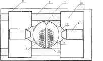
一种纳米材料原位结构性能测试的透射电镜载片,其特征在于,该载片包括中心金属片1、两个附耳2、狭缝3、扇形燕尾槽4、沿狭缝3两侧对称分布的至少20个圆形栅孔5;A transmission electron microscope slide for in-situ structural performance testing of nanomaterials, characterized in that the slide includes a
各部分的位置为:分布于中心金属片1左右两侧且处于同一直径上的两个附耳2,包含附耳在内的整个金属片的直径在2.8-3mm之间;垂直于附耳2的直径、沿中心金属片1一侧开口的狭缝3,该狭缝3宽度为2-50μm,长1.2-1.5mm;位于与狭缝3同一直径上且与狭缝3相对的、在中心金属片的另一侧开口的扇形燕尾槽4,所述的扇形燕尾槽缺口半径为0.2-0.3mm,圆心角为30-45°;以及位于狭缝两侧对称分布的40个圆形栅孔5,所述的圆形栅孔每个直径为50-120μm。The positions of each part are: two
实现电学性能测量时,还包括在金属片正面的狭缝两侧蒸镀的绝缘层,绝缘层的厚度为0.05-0.3mm,在绝缘层上再蒸镀电极,蒸镀的电极厚度为0.05-0.3mm。When realizing the measurement of electrical properties, it also includes the insulating layer evaporated on both sides of the slit on the front of the metal sheet. The thickness of the insulating layer is 0.05-0.3mm, and the electrode is evaporated on the insulating layer. 0.3mm.
利用扫描电镜对分布在载片上的纳米线或纳米薄膜进行固定,再利用外力使载片发生变形,使分布在载网上的纳米线或纳米薄膜发生拉伸或压缩变形,借助于透射电镜观测纳米线或薄膜在外力作用下的结构信息和变形过程。Use a scanning electron microscope to fix the nanowires or nanofilms distributed on the slide, and then use external force to deform the slide, so that the nanowires or nanofilms distributed on the slide will be stretched or compressed. Structural information and deformation process of wire or film under external force.
本发明有如下优点:The present invention has following advantage:
1.本发明解决了普通透射电镜载网无法对样品进行操作的缺点,并且可以利用透射电镜双倾样品台实现大角度倾转,在正带轴下观测纳米材料变形前后的力学性质。本发明提供了一种新的、简便的纳米线或薄膜的力、电性能测试方法。1. The present invention solves the disadvantage that the ordinary TEM grid cannot operate the sample, and can use the TEM double-tilt sample stage to realize large-angle tilting, and observe the mechanical properties of nanomaterials before and after deformation under the positive zone axis. The invention provides a new and convenient method for testing the force and electrical properties of the nano wire or thin film.
2.本发明中的金属载片外形尺寸与现有技术载网基本一致,可以方便的装入高分辨透射电镜中,可以实现X,Y两个方向大角度倾转,在原位拉伸变形的同时从最佳的晶带轴实现高分辨成像。2. The outer dimensions of the metal carrier in the present invention are basically the same as those of the prior art carrier grid, and can be easily loaded into a high-resolution transmission electron microscope, and can be tilted at large angles in X and Y directions, and stretched and deformed in situ Simultaneously achieve high-resolution imaging from the best crystal zone axis.
3.本发明中的金属载片具有性能可靠、安装方便、结构简单、操作简便易行的特点,通过拉伸载片中间所开的狭缝实现了对纳米线或纳米薄膜的操作,进一步拓展了透射电镜的功能。3. The metal carrier in the present invention has the characteristics of reliable performance, convenient installation, simple structure, and easy operation. The operation of nanowires or nanofilms is realized by stretching the slit in the middle of the carrier, and further expanded function of the transmission electron microscope.
附图说明Description of drawings
图1力学性能测试载片示意图Figure 1 Schematic diagram of mechanical property test slide
图2压电陶瓷拉伸台上未经拉伸力学性能测试载片俯视示意图Fig. 2 Schematic diagram of the top view of the unstretched mechanical performance test slide on the piezoelectric ceramic stretching table
图3压电陶瓷拉伸台上经过拉伸力学性能测试载片俯视示意图Fig.3 Schematic diagram of top view of slides tested for tensile mechanical properties on piezoelectric ceramic stretching table
图4电学性能测试载片示意图Figure 4 Schematic diagram of electrical performance test slide
图5压电陶瓷拉伸台上未经拉伸电学性能测试载片俯视示意图Figure 5. Schematic diagram of the top view of the unstretched electrical performance test carrier on the piezoelectric ceramic stretching table
图6压电陶瓷拉伸台上经过拉伸电学性能测试载片俯视示意图Figure 6. Schematic diagram of the top view of the stretched electrical performance test carrier on the piezoelectric ceramic stretching table
其中,图面说明如下Among them, the illustrations are as follows
1 中心金属片 2 附耳 3 狭缝 4 扇形燕尾槽 5 圆形栅孔 6 金属压片7 压电陶瓷拉伸台控制系统 8 滑动导轨 9 拉伸滑动台 10 固定台 11 金属电极镀层 12 电极焊点 13 电极引线 14 致密绝缘层1
具体实施方式:Detailed ways:
力学性能的测试实例:将一金属片加工成中心金属片1左右两侧各有一个用来施加应力的附耳2,中心金属片的直径为2mm,连同附耳在内的整个金属片的直径为2.9mm,垂直于附耳2的直径、沿中心金属片1一侧开开一条长为1.3mm,宽为20μm的狭缝3,此狭缝是为了消除因载片的横向变形引起的褶皱变形所设,褶皱变形影响透射电镜对样品的聚焦;在载片的另一侧做一个半径为0.3mm,圆心角35°的扇形燕尾槽4。在靠近狭缝3的附近位置开了40个圆形栅孔5,圆形栅孔的直径为100μm,圆形栅孔的作用是为了能在滴纳米线的时候使溶液更好的流过载片,从而顺利地将纳米线沉积在金属载片上。Test example of mechanical properties: A metal sheet is processed into a
将载片利用压电陶瓷拉伸台上的金属压片6固定在拉伸台装置上,通过压电陶瓷拉伸控制系统7使固定在压电陶瓷拉伸装置上拉伸滑动台9滑动导轨8上沿着远离固定台10的方向发生一定的滑动位移,带动拉伸台上的载片发生变形,变形量可以通过压电陶瓷控制系统7进行精确的控制。这样,两端分别固定在载片窄缝两侧的纳米线或纳米薄膜被拉伸变形,整个过程在扫描电镜进行实时观测,具体实施步骤如下所述:The slide is fixed on the stretching table device by the metal pressing piece 6 on the piezoelectric ceramic stretching table, and the sliding table 9 sliding guide rail fixed on the piezoelectric ceramic stretching device is stretched through the piezoelectric ceramic stretching control system 7 A certain sliding displacement occurs on 8 along the direction away from the fixed table 10, which drives the carrier on the stretching table to deform, and the amount of deformation can be precisely controlled by the piezoelectric
1.将SiC纳米线通过超声震荡后滴在载片上放入透射电镜双倾样品台找到了感兴趣的区域,在[011]正带轴下观察了未发生形变前的SiC纳米线的微观结构。1. Put the SiC nanowires on the slide after being ultrasonically oscillated and put them on the double-tilt sample stage of the transmission electron microscope to find the area of interest, and observe the microstructure of the SiC nanowires before deformation under the [011] positive band axis .
2.将载片从透射电镜样品杆上取出,利用附耳将载片固定在压电陶瓷拉伸台上。2. Take out the slide from the sample rod of the transmission electron microscope, and fix the slide on the piezoelectric ceramic stretching table with the attached ear.
3.将固定好载片的拉伸台放入扫描电镜中,找到了在透射电镜中所记录过的一条长为40μm,直径为100nm的SiC纳米线,聚焦扫描电镜电子束将搭接在载片狭缝两边的SiC纳米线固定好,同时,利用扫描电镜中的微操纵机械手将周围多余的SiC纳米线拨掉,只留待研究的单根SiC纳米线。3. Put the stretching table with the fixed slide into the scanning electron microscope, and find a SiC nanowire with a length of 40 μm and a diameter of 100 nm recorded in the transmission electron microscope. The SiC nanowires on both sides of the slit were fixed, and at the same time, the micro-manipulator in the scanning electron microscope was used to remove the excess SiC nanowires around, leaving only a single SiC nanowire to be studied.
4.在扫描电镜中控制压电陶瓷驱动器,将载片的狭缝拉伸开所需的位移,使固定在两端的SiC纳米线发生单向拉伸变形,利用扫描电镜的成像系统原位的记录了变形过程。4. Control the piezoelectric ceramic driver in the scanning electron microscope to stretch the slit of the slide to the required displacement, so that the SiC nanowires fixed at both ends undergo unidirectional stretching and deformation, and use the imaging system of the scanning electron microscope to in situ The deformation process was recorded.
5.将变形后的载片从拉伸台上取下,放入双倾透射电镜样品台将样品倾转到SiC纳米线[011]正带轴下,通过透射电子显微镜的高分辨原子图像观察SiC纳米线变形后的晶格结构变化。5. Remove the deformed slide from the stretching table, put it into the sample stage of the double-tilt transmission electron microscope, tilt the sample under the positive band axis of the SiC nanowire [011], and observe it through the high-resolution atomic image of the transmission electron microscope Lattice structure changes after deformation of SiC nanowires.
6.通过对变形前后纳米材料微观结构变化的高分辨图像的对比分析,在原子层次上揭示纳米材料在弹塑性变形的特点,变形的尺寸效应,变形过程中位错的产生,以及裂纹的扩展等反映材料力学性能的微观组织结构。6. Through the comparative analysis of the high-resolution images of the microstructural changes of nanomaterials before and after deformation, the characteristics of elastic-plastic deformation of nanomaterials, the size effect of deformation, the generation of dislocations during deformation, and the expansion of cracks are revealed at the atomic level The microstructure reflects the mechanical properties of materials.
通过实施例,发现SiC纳米线发生了超过近5%的弹性和塑性应变,微观结构变化表明SiC在纳米尺度下表现出与大块体材料不同的变形方式。Through the examples, it is found that SiC nanowires undergo elastic and plastic strains exceeding nearly 5%, and the microstructure changes indicate that SiC exhibits different deformation modes from bulk materials at the nanometer scale.
电学性能的测试:在中心金属片1上蒸镀一层致密绝缘层14,绝缘层采用绝缘性能优良的Ti02涂层,厚度为0.1mm;再在此绝缘层的上部沿狭缝3蒸镀两片相互独立的电极,电极采用导电性优良的Au电极,厚度为0.1mm;将Au电极利用点焊机将电极焊点12利用电极引线13与拉伸台的外接电路相连形成所需回路。电学信号的测量实例如下所述:Electrical performance test: Evaporate a layer of dense insulating
1.将电学性能测试载片固定在拉伸台上,接好电路,将拉伸台放入扫描电镜中,利用扫描电镜的微操作机械手将一条长为30μm,直径300nm的ZnO纳米线搭接在狭缝两侧。1. Fix the electrical performance test carrier on the stretching table, connect the circuit, put the stretching table into the scanning electron microscope, and use the micro-manipulator of the scanning electron microscope to overlap a ZnO nanowire with a length of 30 μm and a diameter of 300 nm on both sides of the slit.
2.利用扫描电镜的聚焦电子束将搭接在金属片狭缝上的纳米线两端固定在狭缝的两侧。2. Use the focused electron beam of the scanning electron microscope to fix the two ends of the nanowires lapped on the slit of the metal sheet on both sides of the slit.
3.利用外接电路对处在拉伸台上的载片两电极通电,电压从-5V以0.2Vde的步长升高到5V并记录了电流信号的变化。3. Using an external circuit to energize the two electrodes of the slide on the stretching table, the voltage was increased from -5V to 5V with a step size of 0.2Vde, and the change of the current signal was recorded.
4.控制压电陶瓷拉伸台将载片拉开一定的位移,再次利用外接电路对拉伸台上载片通电,同样电压从-5V以0.2V的步长升高到5V记录电压、电流信号的变化。4. Control the piezoelectric ceramic stretching table to pull the slide to a certain displacement, and then use the external circuit to energize the slide on the stretching table again, and the same voltage increases from -5V to 5V in steps of 0.2V to record the voltage and current signals The change.
通过实施例,测得此ZnO纳米线的电阻为2.8MΩ,ZnO纳米线的I-V曲线没有表现出很好的线形,表现出与普通电阻材料不同的电学性质。Through the embodiment, the measured resistance of the ZnO nanowire is 2.8 MΩ, and the I-V curve of the ZnO nanowire does not show a good line shape, showing different electrical properties from common resistance materials.
另外,以上所述的压电陶瓷拉伸台,还可以用热双金属片驱动的纳米拉伸台等其他拉伸装置替代,实现将金属载片拉伸以拉伸纳米材料的目的。In addition, the piezoelectric ceramic stretching table mentioned above can also be replaced by other stretching devices such as a nano-stretching table driven by a thermal bimetallic sheet, so as to achieve the purpose of stretching the metal carrier to stretch nanomaterials.
Claims (2)
Priority Applications (1)
| Application Number | Priority Date | Filing Date | Title |
|---|---|---|---|
| CNB2007101220920ACN100511567C (en) | 2007-09-21 | 2007-09-21 | Transmission electron microscope slide glass for nano material in-situ structure property test |
Applications Claiming Priority (1)
| Application Number | Priority Date | Filing Date | Title |
|---|---|---|---|
| CNB2007101220920ACN100511567C (en) | 2007-09-21 | 2007-09-21 | Transmission electron microscope slide glass for nano material in-situ structure property test |
Publications (2)
| Publication Number | Publication Date |
|---|---|
| CN101131908A CN101131908A (en) | 2008-02-27 |
| CN100511567Ctrue CN100511567C (en) | 2009-07-08 |
Family
ID=39129117
Family Applications (1)
| Application Number | Title | Priority Date | Filing Date |
|---|---|---|---|
| CNB2007101220920AExpired - Fee RelatedCN100511567C (en) | 2007-09-21 | 2007-09-21 | Transmission electron microscope slide glass for nano material in-situ structure property test |
Country Status (1)
| Country | Link |
|---|---|
| CN (1) | CN100511567C (en) |
Families Citing this family (6)
| Publication number | Priority date | Publication date | Assignee | Title |
|---|---|---|---|---|
| CN106033039A (en)* | 2015-03-09 | 2016-10-19 | 北京航空航天大学 | A micro material stretching method, device and system |
| CN108227113A (en)* | 2016-12-10 | 2018-06-29 | 中国科学院长春光学精密机械与物理研究所 | For the adjustment of mirror optics element angle and the device and method of aberration compensation |
| CN111232438B (en)* | 2020-03-26 | 2024-07-26 | 上海微纳国际贸易有限公司 | High vacuum sample storage device |
| CN112379129B (en)* | 2020-11-16 | 2022-08-23 | 付学文 | High-space-time-resolution multi-mode carrier dynamics measurement system and measurement method |
| CN113138125B (en)* | 2021-04-21 | 2023-03-14 | 北京工业大学 | In-situ double-inclination single-shaft stretching nanowire device and manufacturing method thereof |
| CN113324836B (en)* | 2021-05-28 | 2023-11-10 | 北京工业大学 | Damping device and method for in-situ deformation micro-nano sample in microscope |
- 2007
- 2007-09-21CNCNB2007101220920Apatent/CN100511567C/ennot_activeExpired - Fee Related
Also Published As
| Publication number | Publication date |
|---|---|
| CN101131908A (en) | 2008-02-27 |
Similar Documents
| Publication | Publication Date | Title |
|---|---|---|
| CN101109687B (en) | A device for testing the electromechanical properties of nanowires under in-situ stretching in a transmission electron microscope | |
| CN100520351C (en) | Single-nano-thread in-situ mechanical characteristic detection and structure analysis method and apparatus | |
| CN1963985A (en) | A grid of transmission electronic microscope driven by thermal dual metal sheets | |
| CN100511567C (en) | Transmission electron microscope slide glass for nano material in-situ structure property test | |
| CN105301027B (en) | A kind of transmission/ESEM power, the experiment porch in situ of thermal coupling field loading | |
| CN101113946B (en) | Device for Mechatronic Performance Testing of Nanowires under In-Situ Compression in Transmission Electron Microscopy | |
| CN1995962A (en) | Device and method for testing in-situ mechanical property of single nano-wire in scanning electron microscope | |
| CN100587458C (en) | Nanomaterial Stress Test Grid for Transmission Electron Microscopy | |
| CN100590412C (en) | Device and method for in-situ stretching of nanowires in scanning electron microscope | |
| CN104764660A (en) | Thermal-driving uniaxial drawing/compressive deformation device for scanning/transmission electron microscope | |
| CN101252073A (en) | A Thermally Driven Deformable Transmission Electron Microscope Grid and One-Dimensional Nanomaterial Deformation Method | |
| CN204630827U (en) | A kind of scanning/transmission electron microscope thermal drivers uniaxial tension/compression deformation device | |
| CN201083669Y (en) | Transmission electron microscope nanometer line in situ compressing electromechanical property test device | |
| CN101354416B (en) | Method for preparing small separation distance electrode on transmission electric mirror sample | |
| CN100587459C (en) | Nanomaterial Stretching Device in Scanning Electron Microscope Driven by Piezoelectric Ceramic Sheet | |
| CN201066335Y (en) | A testing device for the electric performance of nano line original position downward pull force in transmission electric lens | |
| CN201083670Y (en) | Transmission electron microscope one-dimensional nano material test slide | |
| CN107782919A (en) | A kind of electricity atomic force microscope probe using conducting nanowires | |
| US11422075B2 (en) | Device and method for determining mechanical properties of nanomaterials | |
| CN201159705Y (en) | In-situ Stress Test of Nanomaterials Transmission Electron Microscopy Grid | |
| Huang et al. | A dual-drive mode MEMS device for in-situ static/dynamic electro-mechanical characterization of nanomaterials | |
| JP2002214112A (en) | Scanning probe microscope | |
| Jin et al. | Mechanical Researches on Young′ s Modulus of SCS Nanostructures | |
| CN101693512A (en) | Compound cantilever beam needle point used for micro-nano microtechnique and manufacturing method thereof | |
| CN201518226U (en) | Composite cantilever beam needlepoint for micro-nano microtechnique |
Legal Events
| Date | Code | Title | Description |
|---|---|---|---|
| C06 | Publication | ||
| PB01 | Publication | ||
| C10 | Entry into substantive examination | ||
| SE01 | Entry into force of request for substantive examination | ||
| C14 | Grant of patent or utility model | ||
| GR01 | Patent grant | ||
| C17 | Cessation of patent right | ||
| CF01 | Termination of patent right due to non-payment of annual fee | Granted publication date:20090708 Termination date:20120921 |