CN100505321C - Vertical color filter sensor group including amorphous silicon semiconductor and manufacturing method thereof - Google Patents
Vertical color filter sensor group including amorphous silicon semiconductor and manufacturing method thereofDownload PDFInfo
- Publication number
- CN100505321C CN100505321CCNB2004800427622ACN200480042762ACN100505321CCN 100505321 CCN100505321 CCN 100505321CCN B2004800427622 ACNB2004800427622 ACN B2004800427622ACN 200480042762 ACN200480042762 ACN 200480042762ACN 100505321 CCN100505321 CCN 100505321C
- Authority
- CN
- China
- Prior art keywords
- transducer
- sensor
- semi
- conducting material
- layer
- Prior art date
- Legal status (The legal status is an assumption and is not a legal conclusion. Google has not performed a legal analysis and makes no representation as to the accuracy of the status listed.)
- Expired - Fee Related
Links
- 239000004065semiconductorSubstances0.000titleclaimsabstractdescription213
- 229910021417amorphous siliconInorganic materials0.000titleclaimsdescription13
- 238000004519manufacturing processMethods0.000titledescription29
- 239000000463materialSubstances0.000claimsabstractdescription179
- 238000000034methodMethods0.000claimsabstractdescription78
- 230000004044responseEffects0.000claimsabstractdescription35
- 230000003595spectral effectEffects0.000claimsabstractdescription33
- 229910021420polycrystalline siliconInorganic materials0.000claimsabstractdescription15
- 229920005591polysiliconPolymers0.000claimsabstractdescription14
- 229910010271silicon carbideInorganic materials0.000claimsabstractdescription4
- VYPSYNLAJGMNEJ-UHFFFAOYSA-NSilicium dioxideChemical compoundO=[Si]=OVYPSYNLAJGMNEJ-UHFFFAOYSA-N0.000claimsdescription84
- 229910052710siliconInorganic materials0.000claimsdescription76
- 239000010703siliconSubstances0.000claimsdescription76
- 230000005855radiationEffects0.000claimsdescription72
- 239000000377silicon dioxideSubstances0.000claimsdescription41
- 230000008569processEffects0.000claimsdescription37
- 239000011343solid materialSubstances0.000claimsdescription17
- 238000010521absorption reactionMethods0.000claimsdescription16
- 239000007787solidSubstances0.000claimsdescription6
- 230000001902propagating effectEffects0.000claimsdescription5
- 239000000758substrateSubstances0.000abstractdescription47
- 238000003491arrayMethods0.000abstractdescription17
- 229910021419crystalline siliconInorganic materials0.000abstractdescription14
- HBMJWWWQQXIZIP-UHFFFAOYSA-Nsilicon carbideChemical compound[Si+]#[C-]HBMJWWWQQXIZIP-UHFFFAOYSA-N0.000abstractdescription3
- 239000010410layerSubstances0.000description323
- XUIMIQQOPSSXEZ-UHFFFAOYSA-NSiliconChemical compound[Si]XUIMIQQOPSSXEZ-UHFFFAOYSA-N0.000description73
- 235000012431wafersNutrition0.000description37
- 238000002955isolationMethods0.000description34
- 230000004888barrier functionEffects0.000description33
- 235000012239silicon dioxideNutrition0.000description33
- 239000007943implantSubstances0.000description18
- 229910052581Si3N4Inorganic materials0.000description17
- 230000003287optical effectEffects0.000description17
- 239000000969carrierSubstances0.000description16
- HQVNEWCFYHHQES-UHFFFAOYSA-Nsilicon nitrideChemical compoundN12[Si]34N5[Si]62N3[Si]51N64HQVNEWCFYHHQES-UHFFFAOYSA-N0.000description15
- 229910052785arsenicInorganic materials0.000description14
- RQNWIZPPADIBDY-UHFFFAOYSA-Narsenic atomChemical compound[As]RQNWIZPPADIBDY-UHFFFAOYSA-N0.000description14
- 230000006870functionEffects0.000description14
- 238000002513implantationMethods0.000description14
- 238000012545processingMethods0.000description14
- 230000000873masking effectEffects0.000description12
- 238000001514detection methodMethods0.000description9
- 238000003384imaging methodMethods0.000description9
- 230000005670electromagnetic radiationEffects0.000description8
- OAICVXFJPJFONN-UHFFFAOYSA-NPhosphorusChemical compound[P]OAICVXFJPJFONN-UHFFFAOYSA-N0.000description7
- 230000008901benefitEffects0.000description7
- 238000006243chemical reactionMethods0.000description7
- 230000036961partial effectEffects0.000description7
- 229910052698phosphorusInorganic materials0.000description7
- 239000011574phosphorusSubstances0.000description7
- 238000002835absorbanceMethods0.000description6
- 239000003989dielectric materialSubstances0.000description6
- 238000009792diffusion processMethods0.000description6
- 230000000694effectsEffects0.000description6
- 239000011810insulating materialSubstances0.000description6
- 238000005468ion implantationMethods0.000description6
- 239000007788liquidSubstances0.000description6
- 229910052751metalInorganic materials0.000description6
- 239000002184metalSubstances0.000description6
- 239000012212insulatorSubstances0.000description5
- 230000035945sensitivityEffects0.000description5
- QVGXLLKOCUKJST-UHFFFAOYSA-Natomic oxygenChemical compound[O]QVGXLLKOCUKJST-UHFFFAOYSA-N0.000description4
- 238000005530etchingMethods0.000description4
- 230000014509gene expressionEffects0.000description4
- BHEPBYXIRTUNPN-UHFFFAOYSA-Nhydridophosphorus(.) (triplet)Chemical compound[PH]BHEPBYXIRTUNPN-UHFFFAOYSA-N0.000description4
- 230000031700light absorptionEffects0.000description4
- 229910052760oxygenInorganic materials0.000description4
- 239000001301oxygenSubstances0.000description4
- 238000002161passivationMethods0.000description4
- 229920002120photoresistant polymerPolymers0.000description4
- 230000009467reductionEffects0.000description4
- 239000011800void materialSubstances0.000description4
- 230000015572biosynthetic processEffects0.000description3
- 239000002800charge carrierSubstances0.000description3
- 239000003086colorantSubstances0.000description3
- 238000013461designMethods0.000description3
- 238000001914filtrationMethods0.000description3
- 239000012530fluidSubstances0.000description3
- 150000004767nitridesChemical class0.000description3
- 230000002829reductive effectEffects0.000description3
- 238000000926separation methodMethods0.000description3
- ZOXJGFHDIHLPTG-UHFFFAOYSA-NBoronChemical compound[B]ZOXJGFHDIHLPTG-UHFFFAOYSA-N0.000description2
- KRHYYFGTRYWZRS-UHFFFAOYSA-NFluoraneChemical compoundFKRHYYFGTRYWZRS-UHFFFAOYSA-N0.000description2
- XYFCBTPGUUZFHI-UHFFFAOYSA-NPhosphineChemical compoundPXYFCBTPGUUZFHI-UHFFFAOYSA-N0.000description2
- 229910004298SiO 2Inorganic materials0.000description2
- 229910052787antimonyInorganic materials0.000description2
- WATWJIUSRGPENY-UHFFFAOYSA-Nantimony atomChemical compound[Sb]WATWJIUSRGPENY-UHFFFAOYSA-N0.000description2
- 230000005540biological transmissionEffects0.000description2
- 229910052796boronInorganic materials0.000description2
- 230000008859changeEffects0.000description2
- 239000002131composite materialSubstances0.000description2
- 230000008878couplingEffects0.000description2
- 238000010168coupling processMethods0.000description2
- 238000005859coupling reactionMethods0.000description2
- 239000013078crystalSubstances0.000description2
- 238000000151depositionMethods0.000description2
- 230000008021depositionEffects0.000description2
- 238000010586diagramMethods0.000description2
- 238000009826distributionMethods0.000description2
- 239000002019doping agentSubstances0.000description2
- 239000000975dyeSubstances0.000description2
- 238000005516engineering processMethods0.000description2
- 229910052738indiumInorganic materials0.000description2
- APFVFJFRJDLVQX-UHFFFAOYSA-Nindium atomChemical compound[In]APFVFJFRJDLVQX-UHFFFAOYSA-N0.000description2
- 230000010354integrationEffects0.000description2
- 230000004048modificationEffects0.000description2
- 238000012986modificationMethods0.000description2
- 238000005498polishingMethods0.000description2
- 230000002441reversible effectEffects0.000description2
- 150000003376siliconChemical class0.000description2
- 229910052814silicon oxideInorganic materials0.000description2
- 241000894007speciesSpecies0.000description2
- 238000001228spectrumMethods0.000description2
- 239000000126substanceSubstances0.000description2
- 238000012546transferMethods0.000description2
- 238000012935AveragingMethods0.000description1
- 241000338702Cupido minimusSpecies0.000description1
- MCVAAHQLXUXWLC-UHFFFAOYSA-N[O-2].[O-2].[S-2].[Gd+3].[Gd+3]Chemical compound[O-2].[O-2].[S-2].[Gd+3].[Gd+3]MCVAAHQLXUXWLC-UHFFFAOYSA-N0.000description1
- 230000002745absorbentEffects0.000description1
- 239000002250absorbentSubstances0.000description1
- 238000000862absorption spectrumMethods0.000description1
- RBFQJDQYXXHULB-UHFFFAOYSA-NarsaneChemical compound[AsH3]RBFQJDQYXXHULB-UHFFFAOYSA-N0.000description1
- 238000010420art techniqueMethods0.000description1
- XQPRBTXUXXVTKB-UHFFFAOYSA-Mcaesium iodideChemical compound[I-].[Cs+]XQPRBTXUXXVTKB-UHFFFAOYSA-M0.000description1
- 238000005229chemical vapour depositionMethods0.000description1
- 229910052681coesiteInorganic materials0.000description1
- 230000000295complement effectEffects0.000description1
- 238000007796conventional methodMethods0.000description1
- 229910052906cristobaliteInorganic materials0.000description1
- 230000007423decreaseEffects0.000description1
- 230000007547defectEffects0.000description1
- 230000005684electric fieldEffects0.000description1
- 230000007613environmental effectEffects0.000description1
- 238000011049fillingMethods0.000description1
- 239000007789gasSubstances0.000description1
- 238000010438heat treatmentMethods0.000description1
- 125000005842heteroatomChemical group0.000description1
- 150000004678hydridesChemical class0.000description1
- 238000005286illuminationMethods0.000description1
- 239000012535impuritySubstances0.000description1
- 238000002347injectionMethods0.000description1
- 239000007924injectionSubstances0.000description1
- 238000009434installationMethods0.000description1
- 239000011229interlayerSubstances0.000description1
- 230000001788irregularEffects0.000description1
- 238000003475laminationMethods0.000description1
- 238000005259measurementMethods0.000description1
- 239000012528membraneSubstances0.000description1
- 238000001465metallisationMethods0.000description1
- 230000005012migrationEffects0.000description1
- 238000013508migrationMethods0.000description1
- 239000000203mixtureSubstances0.000description1
- 229910021421monocrystalline siliconInorganic materials0.000description1
- 229910000073phosphorus hydrideInorganic materials0.000description1
- 239000000049pigmentSubstances0.000description1
- 238000000623plasma-assisted chemical vapour depositionMethods0.000description1
- 238000005036potential barrierMethods0.000description1
- 238000002360preparation methodMethods0.000description1
- 239000011241protective layerSubstances0.000description1
- 238000002310reflectometryMethods0.000description1
- 230000014624response to red lightEffects0.000description1
- 238000005070samplingMethods0.000description1
- 229910052594sapphireInorganic materials0.000description1
- 239000010980sapphireSubstances0.000description1
- 239000002210silicon-based materialSubstances0.000description1
- 238000004088simulationMethods0.000description1
- 239000002002slurrySubstances0.000description1
- 238000004544sputter depositionMethods0.000description1
- 229910052682stishoviteInorganic materials0.000description1
- 230000000153supplemental effectEffects0.000description1
- 229910052905tridymiteInorganic materials0.000description1
- 230000000007visual effectEffects0.000description1
Images


Classifications
- H—ELECTRICITY
- H10—SEMICONDUCTOR DEVICES; ELECTRIC SOLID-STATE DEVICES NOT OTHERWISE PROVIDED FOR
- H10F—INORGANIC SEMICONDUCTOR DEVICES SENSITIVE TO INFRARED RADIATION, LIGHT, ELECTROMAGNETIC RADIATION OF SHORTER WAVELENGTH OR CORPUSCULAR RADIATION
- H10F39/00—Integrated devices, or assemblies of multiple devices, comprising at least one element covered by group H10F30/00, e.g. radiation detectors comprising photodiode arrays
- H10F39/80—Constructional details of image sensors
- H10F39/807—Pixel isolation structures
- H—ELECTRICITY
- H10—SEMICONDUCTOR DEVICES; ELECTRIC SOLID-STATE DEVICES NOT OTHERWISE PROVIDED FOR
- H10F—INORGANIC SEMICONDUCTOR DEVICES SENSITIVE TO INFRARED RADIATION, LIGHT, ELECTROMAGNETIC RADIATION OF SHORTER WAVELENGTH OR CORPUSCULAR RADIATION
- H10F30/00—Individual radiation-sensitive semiconductor devices in which radiation controls the flow of current through the devices, e.g. photodetectors
- H10F30/20—Individual radiation-sensitive semiconductor devices in which radiation controls the flow of current through the devices, e.g. photodetectors the devices having potential barriers, e.g. phototransistors
- H10F30/21—Individual radiation-sensitive semiconductor devices in which radiation controls the flow of current through the devices, e.g. photodetectors the devices having potential barriers, e.g. phototransistors the devices being sensitive to infrared, visible or ultraviolet radiation
- H—ELECTRICITY
- H10—SEMICONDUCTOR DEVICES; ELECTRIC SOLID-STATE DEVICES NOT OTHERWISE PROVIDED FOR
- H10F—INORGANIC SEMICONDUCTOR DEVICES SENSITIVE TO INFRARED RADIATION, LIGHT, ELECTROMAGNETIC RADIATION OF SHORTER WAVELENGTH OR CORPUSCULAR RADIATION
- H10F39/00—Integrated devices, or assemblies of multiple devices, comprising at least one element covered by group H10F30/00, e.g. radiation detectors comprising photodiode arrays
- H10F39/011—Manufacture or treatment of image sensors covered by group H10F39/12
- H10F39/014—Manufacture or treatment of image sensors covered by group H10F39/12 of CMOS image sensors
- H—ELECTRICITY
- H10—SEMICONDUCTOR DEVICES; ELECTRIC SOLID-STATE DEVICES NOT OTHERWISE PROVIDED FOR
- H10F—INORGANIC SEMICONDUCTOR DEVICES SENSITIVE TO INFRARED RADIATION, LIGHT, ELECTROMAGNETIC RADIATION OF SHORTER WAVELENGTH OR CORPUSCULAR RADIATION
- H10F39/00—Integrated devices, or assemblies of multiple devices, comprising at least one element covered by group H10F30/00, e.g. radiation detectors comprising photodiode arrays
- H10F39/10—Integrated devices
- H10F39/12—Image sensors
- H10F39/18—Complementary metal-oxide-semiconductor [CMOS] image sensors; Photodiode array image sensors
- H10F39/182—Colour image sensors
- H10F39/1825—Multicolour image sensors having stacked structure, e.g. NPN, NPNPN or multiple quantum well [MQW] structures
Landscapes
- Solid State Image Pick-Up Elements (AREA)
- Light Receiving Elements (AREA)
- Transforming Light Signals Into Electric Signals (AREA)
Abstract
Translated fromChinese
Description
Translated fromChinese技术领域technical field
本发明涉及包括垂直堆叠的传感器的光敏传感器组。在每一组中,半导体材料对垂直入射的电磁辐射进行滤色(或者,其它材料也对该辐射进行过滤),并且每一个传感器同时检测不同的波带。本发明也涉及这种传感器组的阵列,其中每一个传感器组定位于不同的像素位置。The present invention relates to photosensitive sensor groups comprising vertically stacked sensors. In each group, the semiconductor material filters normally incident electromagnetic radiation (or other materials also filter the radiation), and each sensor simultaneously detects a different waveband. The invention also relates to an array of such sensor groups, where each sensor group is positioned at a different pixel location.
背景技术Background technique
在本文中,“滤光片”和“滤色片”这样的表述可在广义上互换使用,以表示一种对入射到其上的电磁辐射中的至少一个波带进行选择性地透射或反射的元件。例如,一种类型的滤光片是分色镜,它既透射第一波带中的辐射,又反射第二波带中的辐射。滤光片的示例包括使短波通过的滤光片、使长波通过的滤光片以及带通滤光片。As used herein, the expressions "optical filter" and "color filter" are used interchangeably in a broad sense to mean a device that selectively transmits or transmits at least one band of electromagnetic radiation incident thereon. reflective element. For example, one type of filter is a dichroic mirror, which both transmits radiation in a first waveband and reflects radiation in a second waveband. Examples of optical filters include filters that pass short wavelengths, filters that pass long wavelengths, and bandpass filters.
本文中使用术语“辐射”来表示电磁辐射。The term "radiation" is used herein to denote electromagnetic radiation.
在本文中,(传感器组的)“顶部传感器”这样的表述是指入射到该传感器组的辐射在到达该组任何其它传感器之前先到达的那个传感器。传感器组的传感器是“垂直堆叠的”这种表述是指,这些传感器之一是该组的顶部传感器并且该组具有至少一个穿过所有传感器而延伸的轴(有时被称为“垂直轴”)。如下所述,用来实施本发明的垂直滤色片(VCF)传感器组最好包括垂直堆叠的传感器,这些传感器被配置成使得该组的顶部传感器具有一个可定义法线轴的顶部表面(例如,该顶部表面至少基本上是平的),并且当沿该组的垂直轴传播的辐射入射到该组时,该辐射以相对于该法线轴约小于30度的入射角入射到顶部传感器上(例如,该辐射正入射到该组)。In this context, the expression "top sensor" (of a sensor group) refers to the sensor to which radiation incident on the sensor group reaches before reaching any other sensor in the group. The expression that the sensors of a sensor group are "vertically stacked" means that one of the sensors is the top sensor of the group and that the group has at least one axis (sometimes called a "vertical axis") extending through all the sensors . As described below, vertical color filter (VCF) sensor groups used to practice the present invention preferably include vertically stacked sensors configured such that the top sensor of the group has a top surface that defines a normal axis (e.g., The top surface is at least substantially flat), and when radiation propagating along the normal axis of the group is incident on the group, the radiation is incident on the top sensor at an angle of incidence less than about 30 degrees relative to the normal axis (e.g. , the radiation is incident on the group).
在本文中,具有垂直轴的结构中所包括的两个单元是“横向”(或“水平”)分离的这种表述是指,有一个与垂直轴相平行的轴,它在两个单元之间延伸但不会与任一个单元相交。In this context, the statement that two cells included in a structure having a vertical axis are "laterally" (or "horizontally") separated means that there is an axis parallel to the vertical axis that is between the two cells. extends between but does not intersect any cells.
在本文中(包括权利要求书),一产品“包括”一单元是指该产品是或包括该单元。As used herein (including the claims), a product "comprising" a unit means that the product is or includes the unit.
在本领域中,MOS有源像素传感器是公知的。在本领域中,多波带有源像素传感器阵列也是公知的。一种类型的多波带有源像素传感器阵列使用了红光、绿光和蓝光传感器,这些传感器按某一图案水平地置于半导体表面或其附近。使用彩色覆盖式滤光片以便产生在红光、绿光和蓝光传感器之间的颜色选择性。这样的传感器缺点在于,每一个分辨单元占据了相对较大的面积,因为这些传感器一起平铺在一个平面中。另外,从这种传感器阵列中重建彩色图像需要很大的计算强度,并且常常导致带有伪像、缺陷或分辨率较差的图像。MOS active pixel sensors are well known in the art. Multi-band active pixel sensor arrays are also known in the art. One type of multiband active pixel sensor array uses red, green and blue sensors placed horizontally in a pattern on or near a semiconductor surface. Color overlay filters are used to create color selectivity between red, green and blue sensors. A disadvantage of such sensors is that each resolution unit occupies a relatively large area, since the sensors are tiled together in one plane. Additionally, reconstructing color images from such sensor arrays is computationally intensive and often results in images with artifacts, defects, or poor resolution.
另一种类型的多波带像素传感器阵列使用了多个传感器组,每一组包括多个垂直定向排列的传感器。Carr的美国专利4,238,760公布了一种早期的用于检测可见光和红外辐射的多波长垂直传感器组的一个示例,其中表面n型外延区中的第一二极管响应于可见光,第二二极管(包括在下面n型基片中埋入的p区)响应于红外辐射。Carr表示,通过使用一种“与双极IC处理工艺中常见的膜下扩散式集电极接触扩散相似并用于减小参数RCS”的深扩散工艺,来实现对埋入式二极管的接触。Carr也公布了一个实施例,其中V型接触槽(由包括透过n型外延区进行蚀刻这一步骤的工艺来产生该V型接触槽)提供了到埋入式p型区的接触。所公布的器件具有4平方密耳的大小。Carr的专利中所公布的器件具有若干缺点,最值得注意的是它的面积较大,致使它不适用于现代成像系统中图像传感器的密度要求。形成到埋入式红外检测二极管的接触所使用的技术并不适用于现代成像技术或并不适于延伸到3色传感器。Another type of multi-band pixel sensor array uses multiple sensor groups, each group including multiple vertically oriented sensors. U.S. Patent 4,238,760 to Carr discloses an example of an early multi-wavelength vertical sensor array for detecting visible and infrared radiation, in which the first diode in the n-type epitaxial region of the surface responds to visible light, the second diode (including the p-region buried in the underlying n-type substrate) responds to infrared radiation. Contact to the buried diode is achieved by using a deep diffusion process "similar to the under-membrane collector contact diffusion common in bipolar IC processing and used to reduce the parameter RCS ," Carr said. Carr also discloses an embodiment in which a V-shaped contact trench (generated by a process including an etching step through the n-type epitaxial region) provides contact to the buried p-type region. The disclosed device has a size of 4 square mils. The device disclosed in Carr's patent has several disadvantages, most notably its relatively large area, making it unsuitable for the density requirements of image sensors in modern imaging systems. The techniques used to form the contacts to the buried infrared detection diodes are not suitable for modern imaging techniques or extended to 3-color sensors.
Merrill的美国专利5,965,875公布了一种三色可见光传感器组,其中用三重阱CMOS工艺来构造一种结构,其中蓝、绿和红光敏PN结相对于半导体基片的表面(在其上制造成像器)而置于不同的深度。这种三色传感器组允许制造密集的成像阵列,因为这三种颜色是在像平面上大致相同的区域中被检测的。然而,其结构具有若干缺点。首先,该传感器组使用了对绿光敏感的反极性中心PN结来检测并读出绿色信道,这要求改进电路或电压范围,有可能除了通常的NMOS晶体管以外还要包括PMOS晶体管。这种要求不利地增大了传感器面积,并且使包括这些传感器组的检测器中的支援电路复杂化。所增加的电路复杂性使得很难制造出具有灵活的彩色读出能力的图像传感器阵列(如本文所揭示的),并且不可能实现许多现代电子成像应用所要求的很小的传感器尺寸。U.S. Patent 5,965,875 to Merrill discloses a three-color visible light sensor group in which a triple well CMOS process is used to construct a structure in which the blue, green and red photosensitive PN junctions are opposed to the surface of the semiconductor substrate on which the imager is fabricated. ) at different depths. This three-color sensor set allows for the fabrication of dense imaging arrays because the three colors are detected in approximately the same area on the image plane. However, its structure has several disadvantages. First, the sensor group uses a green-sensitive reverse-polarity central PN junction to detect and read out the green channel, which requires a modified circuit or voltage range, possibly including PMOS transistors in addition to the usual NMOS transistors. This requirement disadvantageously increases the sensor area and complicates the supporting circuitry in detectors that include these sensor groups. The added circuit complexity makes it difficult to fabricate image sensor arrays with flexible color readout capabilities (as disclosed herein), and makes it impossible to achieve the small sensor sizes required for many modern electronic imaging applications.
Cao等人的美国专利6,111,300公布了一种彩色有源像素传感器,它使用PIN光电二极管来试图收集蓝光,还使用半导体基片内的两个附加的半导体结二极管(与PIN光电二极管在垂直方向上分隔开)来检测绿光和红光。这种传感器的缺点是:困难且不标准的制造技术;使用了不允许(阵列中)传感器密度很高的结构;无法选择不同的颜色进行读出;以及无法用单片半导体基片进行三种或更多种颜色的检测。U.S. Patent 6,111,300 to Cao et al. discloses a color active pixel sensor that uses a PIN photodiode in an attempt to collect blue light and also uses two additional semiconductor junction diodes within the semiconductor substrate (in the vertical direction to the PIN photodiode separated) to detect green and red light. Disadvantages of such sensors are: difficult and non-standard fabrication techniques; use of structures that do not allow for high sensor density (in an array); inability to select different colors for readout; and inability to use a single semiconductor substrate for three or detection of more colors.
Findlater等人(在2001年IEEE关于电荷耦合器件和先进图像传感器的研讨会上K.M.Findlater、D.Renshaw、J.E.D.Hurwitz、R.K.Henderson、T.E.R.Bailey、S.G.Smith、M.D.Purcell和J.M.Raynor发表了论文“A CMOS Image SensorEmploying a Double Junction Photodiode”,IEEE电子器件协会(2001))公布了一种有源像素传感器,它将双结光电二极管与有机滤光片覆盖结合使用。每一个双结光电二极管包括顶部和底部p型层并在两者之间有n型层。该n型层形成第一光电二极管的阴极,底部p型层形成了第二光电二极管的阳极,第一光电二极管耦合到第一读出电路,而第二光电二极管耦合到第二读出电路。青色和黄色滤光片的嵌合体覆盖传感器阵列,使得在该阵列的每一行中,偶数号的传感器接收第一波带(蓝和绿)的辐射而奇数号的传感器接收第二波带(红和绿)的辐射。这种传感器阵列的性能受限于双结光电二极管较差的颜色响应,并且还受限于n型阱形成这两个光电二极管的阴极这一事实,从而使传感器设计极易受颜色信道之间非线性串扰的影响。另外,作者引述了限制该设计性能和潜在益处的非均匀性和加工/制造局限性。Findlater et al. (K.M. Findlater, D. Renshaw, J.E.D. Hurwitz, R.K. Henderson, T.E.R. Bailey, S.G. Smith, M.D. Purcell and J.M.Raynor published a paper "A CMOS Image Sensor Employing a Double Junction Photodiode", IEEE Electron Devices Society (2001)) discloses an active pixel sensor that combines a double junction photodiode with an organic filter overlay. Each double junction photodiode includes top and bottom p-type layers with an n-type layer in between. The n-type layer forms the cathode of a first photodiode, the bottom p-type layer forms the anode of a second photodiode, the first photodiode is coupled to a first readout circuit, and the second photodiode is coupled to a second readout circuit. A chimera of cyan and yellow filters covers the sensor array such that in each row of the array, even-numbered sensors receive radiation from the first waveband (blue and green) and odd-numbered sensors receive radiation from the second waveband (red and green) radiation. The performance of such sensor arrays is limited by the poor color response of the double-junction photodiode, and also by the fact that the n-type well forms the cathode of these two photodiodes, making the sensor design highly susceptible to color channel differences. Effects of nonlinear crosstalk. Additionally, the authors cite non-uniformity and processing/manufacturing limitations that limit the performance and potential benefits of this design.
在2001年6月18日提交的申请号为09/884,863的美国专利以及上述申请号为10/103,304的美国专利中,描述了若干种类型的垂直滤色片(“VCF”)传感器组及其制造方法。VCF传感器组包括至少两个光敏传感器,它们彼此垂直地堆叠(在相邻的传感器之间使用或不使用非传感器材料)。VCF传感器组的每一个传感器都具有不同的光谱响应。典型地,每一个传感器具有在不同波长处达到峰值的光谱响应。在一些实施例中,VCF传感器组(或者其一个或多个传感器)包括并不充当传感器的滤光片。Several types of vertical color filter ("VCF") sensor groups and their Manufacturing method. A VCF sensor group includes at least two photosensitive sensors stacked vertically on top of each other (with or without non-sensor material between adjacent sensors). Each sensor of the VCF sensor group has a different spectral response. Typically, each sensor has a spectral response that peaks at a different wavelength. In some embodiments, a VCF sensor set (or one or more sensors thereof) includes optical filters that do not act as sensors.
在成像面的相同区域中,VCF传感器组同时检测至少两个波带的光子。相反,时序光子检测法并不在同一时刻对所有波带进行光子检测。(当垂直地观察该成像器时)由成像器中所包括的VCF传感器组所执行的检测发生在该成像器的一个区域中,并且根据到达传感器组内的深度,按波长将这些光子分离开。In the same area of the imaging plane, the VCF sensor group simultaneously detects photons of at least two wavebands. In contrast, time-sequential photon detection does not detect photons in all bands at the same time. (When viewing the imager perpendicularly) The detection performed by the VCF sensor set included in the imager occurs in a region of the imager and the photons are separated by wavelength according to the depth into the sensor set .
典型地,尽管传感器组在检测时通常会具有一些“串扰”,即多个传感器会检测同一波长的光子,但是每一个传感器还是用于检测不同波带中的光子(例如,一个传感器会比其它传感器检测到更多的“蓝色”波带的光子,第二个传感器会比其它传感器检测到更多的“绿色”波带的光子,第三个传感器会比其它传感器检测到更多的“红色”波带的光子)。Typically, each sensor is used to detect photons in a different wavelength band (e.g., one sensor will be more sensitive than the other), although the sensor set will usually have some "crosstalk" in detection, that is, multiple sensors will detect photons of the same wavelength. The sensor detects more photons in the "blue" band, the second sensor detects more photons in the "green" band than the other sensors, and the third sensor detects more photons in the "green" band than the other sensors. photons in the red” band).
VCF传感器组可用于多种成像任务。在较佳的实施例中,它们被用于数码相机(DSC)。然而,它们也可以被用于许多其它系统中,比如线性成像器、摄像机以及机器视觉装备。VCF sensor groups can be used for a variety of imaging tasks. In a preferred embodiment, they are used in digital still cameras (DSC). However, they can also be used in many other systems, such as linear imagers, cameras, and machine vision equipment.
VCF传感器组使用至少一种半导体材料的属性来检测入射光子,并且也在该组不同的深度选择性地检测不同波长的入射光子。不同波长的检测是可行的,因为传感器组的传感器层是垂直堆叠的并且在半导体材料中光吸收深度随波长变化。制造VCF传感器组的成本已减小了很多,因为VCF传感器组不需要外部的滤色片(常规情况下在彩色图像传感器中都要用到外部的滤色片)并且不需要与传感器自身不同的滤色片(传感器自身由可提供滤光功能的半导体材料制成)。然而,在本发明的一些实施例中,VCF传感器组确实包括(或与其一起使用)与传感器自身不同的滤色片。与具有非半导体基滤光片的常规彩色传感器相比,VCF彩色传感器组的光谱响应特征通常更稳定并且更不易受诸如温度或其它环境因素等外部因素的影响(这些外部因素可能存在于制造期间或之后)。The set of VCF sensors uses properties of at least one semiconductor material to detect incident photons, and also selectively detects incident photons of different wavelengths at different depths in the set. Detection of different wavelengths is possible because the sensor layers of the sensor group are vertically stacked and the depth of light absorption varies with wavelength in the semiconductor material. The cost of manufacturing a VCF sensor group has been greatly reduced, because the VCF sensor group does not require external color filters (which are conventionally used in color image sensors) and does not require a different color filter than the sensor itself. Color filter (the sensor itself is made of a semiconductor material that provides light filtering). However, in some embodiments of the invention, the VCF sensor group does include (or is used with) a different color filter than the sensor itself. Compared to conventional color sensors with non-semiconductor-based filters, the spectral response characteristics of VCF color sensor groups are generally more stable and less susceptible to external factors such as temperature or other environmental factors that may exist during manufacturing. or after).
VCF传感器组最好形成于基片(最好是半导体基片)上,并且包括多个垂直堆叠的传感器(例如,传感器层),通过掺杂和/或加偏压将这些传感器配置成收集第一种极性的光生载流子(最好是负电子)。这些传感器包括一个或多个基准层(或多个传感器对被其间隔开),基准层被配置成收集极性相反的光生载流子(最好是正空穴)并将其传导走。这些传感器基于其在传感器组中不伺的深度,还基于包括掺杂程度和加偏压的条件等其它参数,从而具有不同的光谱灵敏度。在操作过程中,这些传感器都单独连接到偏压和有源像素传感器读出电路。在申请号为09/884,863的美国专利以及申请号为10/103,304的在先申请的美国专利中,更为全面地讨论了VCF传感器组及其制造方法。VCF sensor groups are preferably formed on a substrate (preferably a semiconductor substrate) and include a plurality of vertically stacked sensors (e.g., sensor layers) that are doped and/or biased to collect the first A polarity of photogenerated carriers (preferably negative electrons). These sensors include (or pairs of sensors separated by) one or more reference layers configured to collect and conduct away photogenerated carriers of opposite polarity (preferably positive holes). These sensors have different spectral sensitivities based on their depth in the sensor stack, as well as other parameters including doping levels and biasing conditions. During operation, these sensors are individually connected to bias and active pixel sensor readout circuits. VCF sensor groups and methods of making them are discussed more fully in US Patent Application No. 09/884,863 and in prior-filed US Patent Application No. 10/103,304.
如申请号为10/103,304的美国专利中所描述的那样,通过在VCF传感器组的阵列上放置一种滤色片图案,便可以对该阵列进行改进。通过使用仅由单种滤光片材料制成且定位于传感器组的子集之上的滤光片,便可以操作每个传感器组有三个传感器的阵列(通过从该阵列的传感器组内选出的不同子集中读出信号)来检测四个、五个或六个不同波带的辐射。这可以使色彩精度得以提高。任何多种不同类型的滤光片都可以使用,这包括一些常规彩色图像传感器中的有机染料滤光片以及通过半导体集成电路制造工艺与传感器组集成在一起的一层或多层的滤光片(例如,吸收短波长的一层多晶硅,由氧化物和氮化物层交替堆叠而成的干涉滤光片,或通过干涉效应使光谱响应定形的另一种干涉滤光片)。As described in US Patent Application Serial No. 10/103,304, an array of VCF sensor groups can be modified by placing a color filter pattern over the array. By using filters made of only a single filter material and positioned over a subset of sensor groups, it is possible to operate an array with three sensors per sensor group (by selecting The signal is read out in different subsets of the detector) to detect radiation in four, five or six different wavebands. This can improve color accuracy. Any of a variety of different types of filters can be used, including organic dye filters in some conventional color image sensors as well as one or more layers of filters integrated with the sensor group through the semiconductor integrated circuit manufacturing process (eg, a layer of polysilicon that absorbs at short wavelengths, an interference filter made of alternating stacks of oxide and nitride layers, or another interference filter that shapes the spectral response through interference effects).
发明内容Contents of the invention
一种垂直滤色片传感器组形成于基片(最好是半导体基片)上,并且包括至少两个垂直堆叠的光敏传感器,每一个传感器具有不同的光谱响应。在这些传感器中至少有一个传感器包括至少一层除结晶硅以外的半导体材料(例如,碳化硅,或InxGa1-xN,或另一种III-V族半导体材料,或多晶硅,或非晶硅)。本发明的其它方面是这种垂直滤色片传感器组的阵列以及制造这种垂直滤色片传感器组及其阵列的方法。A vertical color filter sensor array is formed on a substrate, preferably a semiconductor substrate, and includes at least two vertically stacked photosensitive sensors, each sensor having a different spectral response. At least one of these sensors includes at least one layer of a semiconductor material other than crystalline silicon (e.g., silicon carbide, orInxGa1-xN , or another III-V semiconductor material, or polysilicon, or non-crystalline silicon). crystalline silicon). Other aspects of the invention are arrays of such vertical color filter sensor groups and methods of making such vertical color filter sensor groups and arrays thereof.
在一类实施例中,传感器组包括一块固体材料,在该材料中形成了至少两个垂直堆叠的传感器,其中每一个传感器都被结构化使得它被配置成加偏压以充当光电二极管,每一个传感器都具有不同的光谱响应,并且在这些传感器中至少有一个传感器包括至少一层除硅以外的半导体材料。In a class of embodiments, the sensor set includes a solid piece of material in which at least two vertically stacked sensors are formed, each sensor structured such that it is configured to be biased to act as a photodiode, each Each of the sensors has a different spectral response, and at least one of the sensors includes at least one layer of a semiconductor material other than silicon.
在另一类实施例中,本发明是在半导体基片上形成的传感器组的阵列,所述传感器组中的每一个都包括至少两个垂直堆叠的传感器,其中每一个传感器都被结构化使得它被配置成加偏压以充当光电二极管,并且在这些传感器中至少有一个传感器包括至少一层除硅以外的半导体材料。至少一个传感器组可以包括至少一个滤光片,该滤光片相对于该组的传感器而定位,使得穿过该滤光片而传播的辐射或从该滤光片反射的辐射将传播到所述那个传感器组中的至少一个传感器内。In another class of embodiments, the invention is an array of sensor groups formed on a semiconductor substrate, each of said sensor groups comprising at least two vertically stacked sensors, wherein each sensor is structured such that it configured to be biased to function as a photodiode, and at least one of the sensors includes at least one layer of a semiconductor material other than silicon. At least one sensor group may comprise at least one optical filter positioned relative to the sensors of the group such that radiation transmitted through or reflected from the filter will propagate to the at least one sensor in that sensor group.
在另一类实施例中,本发明的传感器组包括一块固体材料,在该材料中形成了至少两个垂直堆叠的传感器,其中每一个传感器都被结构化使得它被配置成加偏压以充当光电二极管,并且在这些传感器中至少有一个传感器具有光子吸收区域和雪崩增益区域。In another class of embodiments, the sensor array of the present invention comprises a solid piece of material in which at least two vertically stacked sensors are formed, wherein each sensor is structured such that it is configured to be biased to act as a photodiodes, and at least one of these sensors has a photon absorption region and an avalanche gain region.
在其它实施例中,本发明的传感器组包括一块固体材料,在该材料中形成了至少两个垂直堆叠的传感器,其中每一个传感器都被结构化使得它被配置成加偏压以充当光电二极管,所有的传感器都被配置成收集第一极性的光生载流子,并且在这些传感器中至少有一个传感器包括至少一层主要由多晶硅或非晶硅构成的层。In other embodiments, sensor groups of the present invention comprise a solid piece of material in which at least two vertically stacked sensors are formed, wherein each sensor is structured such that it is configured to be biased to act as a photodiode , all of the sensors are configured to collect photogenerated carriers of a first polarity, and at least one of the sensors includes at least one layer consisting essentially of polysilicon or amorphous silicon.
本发明的另一个方面是图像检测器,它包括至少一个VCF传感器组阵列以及用于将传感器中所产生的光生载流子转换为电信号的电路。Another aspect of the invention is an image detector comprising at least one array of VCF sensor groups and circuitry for converting photogenerated carriers generated in the sensor into electrical signals.
附图说明Description of drawings
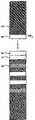
图1是对波长450纳米、550纳米和650纳米而言结晶硅中的电磁辐射强度(相对于其入射强度I0)与在该硅中的深度(单位是微米)之间的函数关系图。FIG. 1 is a graph of the intensity of electromagnetic radiation in crystalline silicon (relative to its incident intensity I0 ) as a function of the depth (in microns) in the silicon for wavelengths of 450 nm, 550 nm and 650 nm.
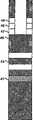
图2是用来实施本发明的VCF传感器组的垂直掺杂分布图。Figure 2 is a graph of the vertical doping profile of a VCF sensor group used to practice the invention.
图2A是具有图2所示分布的VCF传感器组(在垂直平面中的)横截面图,其中示出了耦合到该传感器组的偏压和读出电路的示意性电路图。2A is a cross-sectional view (in the vertical plane) of a VCF sensor group having the distribution shown in FIG. 2, showing a schematic circuit diagram of bias and readout circuitry coupled to the sensor group.
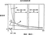
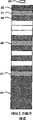
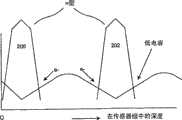
图3是对波长450纳米(曲线A)、550纳米(曲线B)和650纳米(曲线C)而言结晶硅中的电磁辐射吸收率(相对于其入射强度I0)与在该硅中的深度(单位是微米)之间的函数关系图,其上标明了图2所示传感器组各覆盖层的位置。Fig. 3 is for
图4是其分布与图2所示相似的传感器组的三个光电二极管的光谱响应图。FIG. 4 is a graph of the spectral response of three photodiodes of a sensor group whose distribution is similar to that shown in FIG. 2 .
图5是本发明的VCF传感器组的实施例(在垂直平面中的)简化后的横截面图。Figure 5 is a simplified cross-sectional view (in a vertical plane) of an embodiment of a VCF sensor group of the present invention.
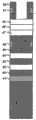
图6是一张表格,它(在中间一栏)以电子伏特为单位列出了铟含量不同的InxGa1-xN半导体中的带隙能量,并(在右边一栏)列出了与各个带隙能量相对应的光波长。Figure 6 is a table which lists (in the middle column) the bandgap energies in eV forInxGa1- xN semiconductors with different indium contents and (in the right column) The wavelength of light corresponding to the energy of each bandgap.
图7是在本发明的VCF传感器组的实施例中可以包括的雪崩传感器的横截面图。Figure 7 is a cross-sectional view of an avalanche sensor that may be included in an embodiment of the VCF sensor pack of the present invention.
图8是本发明的VCF传感器组阵列的部分横截面图,该阵列中的每一个传感器组包括两个非传感器滤光片和三个传感器。8 is a partial cross-sectional view of an array of VCF sensor groups of the present invention, each sensor group in the array comprising two non-sensor filters and three sensors.
图8A是本发明的VCF传感器组阵列的部分简化顶视图,其中包括滤光片的每一个组都用“X”来标记。Figure 8A is a simplified top view of a portion of an array of VCF sensor groups of the present invention, with each group including a filter marked with an "X".
图8B是本发明的VCF传感器组的另一种阵列的部分简化顶视图,其中包括滤光片的每一个组都用“X”来标记。Fig. 8B is a simplified top view of a portion of another array of VCF sensor groups of the present invention, where each group including a filter is marked with an "X".
图9是本发明的VCF传感器组阵列的部分横截面图,其中在该阵列的每一个传感器组上形成一个微透镜。Fig. 9 is a partial cross-sectional view of a VCF sensor group array of the present invention wherein a microlens is formed on each sensor group of the array.
图10是本发明的VCF传感器组阵列的部分简化顶视图,其中相邻的传感器组共享载流子收集单元。Figure 10 is a simplified top view of a portion of an array of VCF sensor groups of the present invention, wherein adjacent sensor groups share a carrier collection unit.
图10A是阵列中两个VCF传感器组(在垂直平面中)的横截面图,其中两个传感器组共享一个公用的传感器单元。Figure 10A is a cross-sectional view (in the vertical plane) of two VCF sensor groups in an array, where the two sensor groups share a common sensor cell.
图10B是阵列中四个VCF传感器组的顶视图,其中这四个传感器组共享载流子收集区域,该载流子收集区域用于收集通过红光和蓝光光子吸收而产生的光生载流子。Figure 10B is a top view of four VCF sensor groups in the array, where the four sensor groups share a carrier collection area for collecting photogenerated carriers generated by red and blue photon absorption .
图11是常规传感器阵列(在垂直平面中)的部分横截面图。Figure 11 is a partial cross-sectional view (in a vertical plane) of a conventional sensor array.
图12是VCF传感器组的阵列(在垂直平面中)的部分横截面图,在该阵列中相邻的传感器组之间有沟槽隔离结构。12 is a partial cross-sectional view (in a vertical plane) of an array of VCF sensor groups with trench isolation structures between adjacent sensor groups in the array.
图13a-13f是本发明的VCF传感器组的实施例在各个制造步骤中所形成的结构(在垂直平面中)的横截面图。13a-13f are cross-sectional views (in the vertical plane) of structures (in the vertical plane) formed during various fabrication steps of an embodiment of the VCF sensor group of the present invention.
图14A-14L是本发明的VCF传感器组的另一个实施例在各个制造步骤中所形成的结构(在垂直平面中)的横截面图。14A-14L are cross-sectional views (in the vertical plane) of structures (in the vertical plane) formed during various fabrication steps of another embodiment of the VCF sensor group of the present invention.
图15A-15H是本发明的VCF传感器组的另一个实施例在各个制造步骤中所形成的结构(在垂直平面中)的横截面图。15A-15H are cross-sectional views (in the vertical plane) of structures (in the vertical plane) formed during various fabrication steps of another embodiment of the VCF sensor group of the present invention.
图16A-16H是本发明的VCF传感器组的另一个实施例的各个制造步骤中所形成的结构(在垂直平面中)的横截面图。16A-16H are cross-sectional views (in the vertical plane) of structures formed during various fabrication steps of another embodiment of a VCF sensor group of the present invention.
图17是在制造VCF传感器组的实施例期间所形成的结构(在垂直平面中)的横截面图,其中包括通过注入工艺而形成的插头。每一条轮廓线(用于表示p型和n型材料之间的边界)显示用不同类型掺杂程度形成插头的结果,其中最小的n型区域具有第一(“1x”)n型掺杂程度,最大的n型区域具有该掺杂程度的两倍(“2x”),而大小居中的n型区域具有中等的(“1.4x”)n型掺杂程度。17 is a cross-sectional view (in a vertical plane) of a structure formed during fabrication of an embodiment of a VCF sensor group, including plugs formed by an implantation process. Each contour line (used to represent the boundary between p-type and n-type materials) shows the result of forming plugs with different types of doping levels, where the smallest n-type region has a first ("1x") n-type doping level , the largest n-type region has twice that doping ("2x"), while the n-type region in the middle size has a medium ("1.4x") n-type doping.
图18是在制造本发明的VCF传感器组的较佳实施例期间所形成的一种结构(在垂直平面中)的横截面图,其中包括插头的底部(它形成于多级注入工艺的前期)。Figure 18 is a cross-sectional view (in the vertical plane) of a structure formed during fabrication of a preferred embodiment of the VCF sensor group of the present invention, including the bottom of the plug (which is formed early in the multi-level implantation process) .
图18A是在制造本发明的VCF传感器组的较佳实施例期间从图18所示结构中形成的一种结构(在垂直平面中)的横截面图,其中包括插头的顶部(它形成于多级注入工艺的下一级期间),该插头的底部在图18和18A中都有示出。18A is a cross-sectional view (in the vertical plane) of a structure (in the vertical plane) formed from the structure shown in FIG. 18 during the manufacture of a preferred embodiment of the VCF sensor group of the present invention, including the top of the During the next stage of the stage implant process), the bottom of the plug is shown in both Figures 18 and 18A.
图19示出了对五种所示掩模材料而言在硼、磷、砷和锑的典型注入过程中所要求的掩模厚度。Figure 19 shows the mask thicknesses required during a typical implant of boron, phosphorous, arsenic and antimony for the five mask materials shown.
图20是本发明的VCF传感器组的实施例(在垂直平面中)的简化横截面图,其中在两个传感器之间包括了掩盖阻挡层(205)。Figure 20 is a simplified cross-sectional view (in the vertical plane) of an embodiment (in the vertical plane) of a VCF sensor group of the present invention in which a masking barrier (205) is included between the two sensors.
图21是掺杂浓度与图20所示传感器组中的深度之间的函数关系图。FIG. 21 is a graph of doping concentration as a function of depth in the sensor group shown in FIG. 20 .
图22是图20所示传感器组的变体(在垂直平面中)的简化横截面图,其中包括常规的掩盖阻挡层注入而非本发明的掩盖阻挡层205。Fig. 22 is a simplified cross-sectional view (in the vertical plane) of a variation (in the vertical plane) of the sensor group shown in Fig. 20, which includes a conventional mask barrier implant instead of the
图23是掺杂浓度与图22所示传感器组中的深度之间的函数关系图。FIG. 23 is a graph of doping concentration as a function of depth in the sensor group shown in FIG. 22 .
图24是本发明的VCF传感器组的另一个实施例(在垂直平面中)的简化横截面图,其中包括了在两个传感器之间的掩盖阻挡层(205)以及另外的掩盖阻挡层注入(207和208)。Figure 24 is a simplified cross-sectional view (in the vertical plane) of another embodiment (in the vertical plane) of a VCF sensor group of the present invention, which includes a masking barrier (205) between two sensors and an additional masking barrier implant ( 207 and 208).
图25A-25D是在制造本发明的VCF传感器组的实施例期间自对准补充注入工艺的各个步骤中所形成的结构(在垂直平面中)的横截面图。25A-25D are cross-sectional views (in the vertical plane) of structures formed during various steps of a self-aligned supplemental implant process during fabrication of an embodiment of a VCF sensor group of the present invention.
具体实施方式Detailed ways
本领域的一般技术人员将会意识到,下文关于本发明的描述只是说明性的,并且在任何方面都不是限制性的。对于从本发明中获益的技术人员而言,将很容易想到本发明的其它实施例。Those of ordinary skill in the art will appreciate that the following description of the invention is illustrative only and not restrictive in any way. Other embodiments of the invention will readily occur to those skilled in the art having the benefit of the invention.
本文中要描述的大部分制造过程都假设传感器由结晶硅制成,但是该方法(或对于本领域的技术人员显而易见的关于该方法的修改)通常也可以应用于由其它半导体材料制成的传感器。VCF传感器组的每一个传感器都通过直接或间接地将光子的能量转变为电子空穴对来检测光子。这发生在半导电材料中。VCF传感器组通常实现为,使得该组中每一个传感器的输出表示入射辐射的不同波带。到达VCF传感器组中每一个传感器的辐射因形成传感器组的材料具有滤光作用而具有不同的波长强度谱。因此,在VCF传感器组中所有的传感器可以是完全相同的,并且各传感器仍然可以产生表示不同波带的输出。然而,在一些实施例中,VCF传感器组中的传感器并非全都相同(例如,它们并非都由相同的材料或材料组合而构成),并且针对预定的应用来确定各传感器的结构和组分以便使传感器组的性能达到最佳或有所改善。例如,对给定范围的波长灵敏度相对较高(即在该范围中吸光率相对较高)而对其它波长灵敏度较低的传感器,可以与具有不同光谱灵敏度的其它材料所制成的传感器垂直地堆叠在一起,从而形成VCF传感器组。Most of the fabrication process to be described herein assumes that the sensor is made of crystalline silicon, but the method (or modifications to it that will be obvious to those skilled in the art) can generally be applied to sensors made of other semiconductor materials as well. . Each sensor of the VCF sensor group detects photons by directly or indirectly converting the energy of the photons into electron-hole pairs. This occurs in semiconducting materials. Groups of VCF sensors are typically implemented such that the output of each sensor in the group represents a different waveband of incident radiation. The radiation reaching each sensor in the VCF sensor group has a different wavelength intensity spectrum due to the filtering effect of the material forming the sensor group. Thus, all sensors in a VCF sensor bank can be identical, and each sensor can still produce outputs representing different wavebands. However, in some embodiments, the sensors in the VCF sensor group are not all identical (e.g., they are not all composed of the same material or combination of materials), and the structure and composition of each sensor is determined for the intended application so that The performance of the sensor group is at its best or improved. For example, a sensor that is relatively sensitive to a given range of wavelengths (i.e., has a relatively high absorbance in that range) and less sensitive to other wavelengths can be vertically integrated with sensors made of other materials with different spectral sensitivities. stacked together to form a VCF sensor group.
数码相机(DSC)的彩色输出因人类视觉系统的三色本质而要求最少检测三个光谱带。因此,本发明的VCF传感器组的许多实施例都具有三个垂直堆叠的传感器(每一个都包括半导体材料),以便检测三个不同的光谱带。具有两个而非三个垂直堆叠的传感器的VCF传感器组可用于其它场合,比如用于对可见光和红外辐射同时进行检测,这在美国专利4,581,625和美国专利4,677,289中有所描述。因为检测不止三个光谱区域可能是有利的,所以本发明的VCF传感器组的一些实施例具有不止三个垂直堆叠的传感器。通过使用来自附加光谱区域的额外信息,便有可能更精确地表示某一物体的颜色。因为可以获得更多的光谱数据,所以颜色表示的精确度有望提高。The color output of a digital camera (DSC) requires detection of a minimum of three spectral bands due to the trichromatic nature of the human visual system. Accordingly, many embodiments of the VCF sensor group of the present invention have three vertically stacked sensors (each comprising semiconductor material) in order to detect three different spectral bands. VCF sensor groups with two rather than three vertically stacked sensors can be used in other applications, such as for simultaneous detection of visible and infrared radiation, as described in US Patent 4,581,625 and US Patent 4,677,289. Because detecting more than three spectral regions may be advantageous, some embodiments of the VCF sensor group of the present invention have more than three vertically stacked sensors. By using additional information from additional spectral regions, it is possible to more accurately represent the color of an object. As more spectral data becomes available, the accuracy of color representation is expected to increase.
在本发明的VCF传感器组的一类实施例中,每一个传感器包括两层半导体材料(比如,有的传感器包括图2中的层X01以及层X09与X01相邻的那部分)或三层半导体材料(比如,有的传感器包括层X02以及层X09、X10分别与X02相邻的那部分),在传感器中每两个相邻的层之间都有一个结(例如,“p-n”结或异质结),并且传感器的这些层中的一层是具有接触部分(它可接入偏压和读出电路)的载流子收集单元。在典型的操作过程中,各传感器的多个层都加上偏压,使得光生载流子穿过至少一个耗尽区迁移到该接触部分,从而在该接触部分处可获得光电荷信号。在VCF传感器组的典型实施例中,该组包括这样的材料(例如,在图2所示的层X09中既不属于耗尽区X04也不属于耗尽区X05的半导体材料),在这种材料中光子可以被吸收并且这种吸收很可能产生可由读出电路检测到的电荷,但是在这种材料中光生载流子可以朝着至少两个不同的载流子收集单元中的任一个迁移(可能性极大)。通常,但不是必然地,VCF传感器组中所有的层都由半导体材料组成。In a class of embodiments of the VCF sensor group of the present invention, each sensor includes two layers of semiconductor material (for example, some sensors include layer X01 in FIG. 2 and the part of layer X09 adjacent to X01) or three layers of semiconductor material. materials (for example, some sensors include layer X02 and layers X09, X10 adjacent to X02 respectively), there is a junction between every two adjacent layers in the sensor (for example, "p-n" junction or heterogeneous Junction), and one of these layers of the sensor is a carrier collection unit with a contact portion that can be accessed for biasing and readout circuitry. During typical operation, the layers of each sensor are biased such that photogenerated carriers migrate across at least one depletion region to the contact, where a photocharge signal is available. In a typical embodiment of a VCF sensor group, the group includes materials (for example, semiconductor materials that belong to neither the depletion region X04 nor the depletion region X05 in layer X09 shown in FIG. A material in which photons can be absorbed and this absorption is likely to generate a charge that can be detected by a readout circuit, but in this material photogenerated carriers can migrate towards either of at least two different carrier collection units (very likely). Typically, but not necessarily, all layers in a VCF sensor group consist of semiconductor materials.
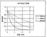
图1是对于波长450纳米、550纳米和650纳米而言在结晶硅中电磁辐射强度(相对于其入射强度I0)与在该硅中的深度之间的函数关系图。图3是对于波长450纳米(曲线A)、550纳米(曲线B)和650纳米(曲线C)而言在结晶硅中的电磁辐射吸收率(相对于其入射强度I0)与在该硅中的深度之间的函数关系图,其上标明了图2所示在其上覆盖了传感器组的各层的位置。图1和3的图是从相同的数据中得出的。图3的每一条曲线画出了多个差值,其中第“n”个差值是图1所示相应曲线的第“(n+1)”个和第“n”个数据值之差。在除硅以外的许多半导体中,(具有给定波长的)辐射的强度与深度的函数关系与图1所示很相似。图1示出了(对于各个波长而言)辐射的相对强度(比例I/I0,其中I是在硅中深度“x”处的强度,I0是入射强度)随深度的增大而减小,因为光子被硅吸收了。图1和3示出了与波长更长的光子相比,在表面附近有相对更多的蓝光(450纳米)光子被吸收,还示出了在硅中任何深度,绿光(550纳米)光子都要比蓝光光子要多,并且红光(650纳米)光子比绿光光子要多(假定红光、绿光和蓝光光子的入射强度相等)。FIG. 1 is a graph of the intensity of electromagnetic radiation in crystalline silicon (relative to its incident intensity I0 ) as a function of depth in the silicon for wavelengths of 450 nm, 550 nm and 650 nm. Fig. 3 is for
图1(和图3)的三条曲线中的每一条曲线都表明随深度的增大强度呈指数衰减,并且每一条曲线都基于在经典型的掺杂和处理后的结晶硅中对光测得的行为。每一条曲线的精确形状将取决于掺杂和处理的参数,但是在假定掺杂和/或处理参数组不相同的各曲线之间将会只有很小的差异。众所周知,半导体对不同波长的光子的吸收取决于该半导体材料的带隙能量以及带边状态的细节。同样众所周知的是,典型的半导体(例如硅)对不同的波长具有不同的吸光率。Each of the three curves in Figure 1 (and Figure 3) shows an exponential decay in intensity with depth, and each curve is based on optical measurements in classically doped and treated crystalline silicon the behavior of. The exact shape of each curve will depend on the doping and processing parameters, but there will be only small differences between the curves assuming a different set of doping and/or processing parameters. It is well known that the absorption of photons of different wavelengths by a semiconductor depends on the band gap energy of the semiconductor material and the details of the band edge states. It is also well known that typical semiconductors such as silicon have different absorbances for different wavelengths.
从图1和3中可明显看出,在体积较大的硅中给定的深度处,充当VCF传感器组中的一个传感器且具有给定厚度的某一体积的硅,对蓝光的吸光率大于绿光,并且对绿光的吸光率大于红光。然而,如果在较大的体积中传感器硅足够地深,则大部分蓝光和绿光都将被该传感器硅上面的材料吸收。即使具有基本上平的波长-强度谱的光入射到较大体积的表面上,只要到达传感器的绿光和蓝光的强度比到达传感器的红光的强度小很多,传感器实际上也会吸收比绿光或蓝光要多的红光。It is evident from Figures 1 and 3 that at a given depth in a larger volume of silicon, a volume of silicon serving as a sensor in a VCF sensor group and having a given thickness absorbs more than Green light, and the absorbance of green light is greater than that of red light. However, if the sensor silicon is sufficiently deep in a larger volume, most of the blue and green light will be absorbed by the material above the sensor silicon. Even if light with a substantially flat wavelength-intensity spectrum is incident on a surface of a larger volume, the sensor will actually absorb more light than the green light as long as the intensity of the green and blue light reaching the sensor is much smaller than the intensity of the red light reaching the sensor. More red light than light or blue light.
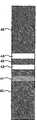
本发明的VCF传感器组的典型实施例通过在半导体材料的体积中不同范围的深度处捕获光子,来实现色彩的分离。图2是VCF传感器组的垂直掺杂分布图,它包括顶层X01(由n型半导体构成)、在顶层下面的第二(p型)层X09、在第二层下面的第三(n型)层X02、在第三层下面的第四(p型)层X10、在第四层下面的第五(n型)层X03以及在第五层下面的p型半导体基片X11。Typical embodiments of the VCF sensor group of the present invention achieve color separation by trapping photons at different ranges of depths in a volume of semiconductor material. Figure 2 is a vertical doping profile diagram of a VCF sensor group, which includes a top layer X01 (consisting of n-type semiconductor), a second (p-type) layer X09 below the top layer, a third (n-type) layer below the second layer layer X02, a fourth (p-type) layer X10 below the third layer, a fifth (n-type) layer X03 below the fourth layer, and a p-type semiconductor substrate X11 below the fifth layer.
图2A是这种VCF传感器组(在垂直平面中)的横截面图。如图2A所示,偏压和读出电路耦合到层X01、X02、X03、X04和X05以及基片X11。Figure 2A is a cross-sectional view (in the vertical plane) of such a VCF sensor group. As shown in Figure 2A, bias and readout circuitry is coupled to layers X01, X02, X03, X04 and X05 and to substrate X11.
蓝光、绿光和红光光电二极管传感器由图2A所示的n型和p型区之间的结构成,并且置于该半导体结构的表面以下不同的深度处。红光、绿光和蓝光光电荷信号均取自三个隔离的光电二极管的n型阴极(X01、X02和X03)。Blue, green and red photodiode sensors consist of structures between the n-type and p-type regions shown in Figure 2A and are placed at different depths below the surface of the semiconductor structure. Red, green and blue photocharge signals are taken from the n-type cathodes of three isolated photodiodes (X01, X02 and X03).
图2A的读出电路是非存储类型的,与上述美国专利申请09/884,863中所描述的很相似。每一个传感器的读出电路包括:复位晶体管(54b用于蓝光传感器,54g用于绿光传感器,54r用于红光传感器),它们由RESET信号线驱动并且耦合在光电二极管阴极与复位电势(在图2A中以VREF来标识)之间;源极跟随放大晶体管(晶体管56b、56g和56r之一),在操作过程中其栅极耦合到光电二极管阴极而其漏极维持在电势VREF;以及行选晶体管(晶体管58b、58g和58r之一),它们由ROW-SELECT信号线驱动并且耦合在相关的源极跟随放大晶体管的源极和行线之间。后缀“r”、“g”和“b”用来表示与各晶体管相关的波带(红、绿或蓝)。如本领域所知的那样,RESET信号是激活的以便使该像素复位,接下来在曝光期间是非激活的,再之后行选线被激活以便读出检测到的信号。The readout circuit of Figure 2A is of the non-memory type, much like that described in the aforementioned US patent application Ser. No. 09/884,863. The readout circuitry for each sensor consists of: reset transistors (54b for the blue sensor, 54g for the green sensor, and 54r for the red sensor) driven by the RESET signal line and coupled between the photodiode cathode and the reset potential (at Between, identified by VREF in FIG. 2A ); a source follows an amplifier transistor (one of
在操作过程中,p型区X09、X10和X11中的每一个都保持地面电势。n型层X01、X02和X03中的每一个都是具有接触部分的载流子收集单元,该接触部分可连接到(并且可以耦合到)偏压和读出电路。在传感器组的每一次读出之前,偏压电路使各个n型层复位到复位电势(在地面电势之上)。当暴露于要被检测的辐射中时,相邻p型和n型层配对经反向偏压便可充当光电二极管:其阴极是层X01且阳极是层X09的第一光电二极管;其阴极是层X02且阳极是层X09和X10的第二光电二极管;以及其阴极是层X03且阳极是层X10和X11的第三光电二极管。如图2所示,n型层X01、X02和X03中的每一个都耦合到偏压和读出电路,因而充当了光电二极管的接线端。During operation, each of the p-type regions X09, X10 and X11 is maintained at ground potential. Each of the n-type layers X01 , X02 and X03 is a carrier collection unit having a contact portion connectable (and coupleable) to bias and readout circuits. A bias circuit resets the individual n-type layers to a reset potential (above ground potential) prior to each readout of the sensor group. When exposed to the radiation to be detected, adjacent p-type and n-type layer pairs are reverse biased to act as photodiodes: a first photodiode whose cathode is layer X01 and anode is layer X09; whose cathode is A second photodiode of layer X02 with anodes of layers X09 and X10; and a third photodiode whose cathode is layer X03 and anode of layers X10 and X11. As shown in Figure 2, each of the n-type layers X01, X02 and X03 is coupled to bias and readout circuitry, thus serving as a terminal for the photodiode.
在典型的操作过程中,当图2的光电二极管反向偏压时,形成了包括该硅的大部分的耗尽区,在该耗尽区中光子被吸收。在图2中,第一光电二极管的耗尽区(主要用来检测蓝光)被标记为“X04”,第二光电二极管的耗尽区(主要用来检测绿光)被标记为“X05”和“X06”,第三光电二极管的耗尽区(主要用来检测红光)被标记为“X07”和“X08”。耗尽区中的电场使通过吸收光子而形成的电子空穴对分开。这便将电荷留在了每一个光电二极管的阴极,并且耦合到每一个阴极的读出电路将该电荷转变为电信号。每一个光电二极管的阴极处的电荷正比于该光电二极管所吸收的光子的数目。该比例是量子效率QE。During typical operation, when the photodiode of Figure 2 is reverse biased, a depletion region is formed comprising most of the silicon in which photons are absorbed. In Figure 2, the depletion region of the first photodiode (mainly used to detect blue light) is marked "X04", the depletion region of the second photodiode (mainly used to detect green light) is marked "X05" and "X06", the depletion region of the third photodiode (mainly used to detect red light) is labeled "X07" and "X08". The electric field in the depletion region separates the electron-hole pairs formed by the absorption of photons. This leaves a charge at the cathode of each photodiode, and readout circuitry coupled to each cathode converts this charge into an electrical signal. The charge at the cathode of each photodiode is proportional to the number of photons absorbed by that photodiode. This ratio is the quantum efficiency QE.
图3示出了与图1所示相同的曲线(它们表示硅对蓝光、绿光和红光光子的吸收),并且也包括用于表示图2所示结构的载流子收集单元(X01、X02和X03)和耗尽区的范围的线条。因此,图3中标记为“X01+X04”的区域表示图2中耗尽区X04的下表面以上的区域,图3中标记为“X05+X02+X06”的区域表示图2中介于耗尽区X05的上表面和耗尽区X06的下表面之间的区域,图3中标记为“X07+X03+X08”的区域表示图2中介于耗尽区X07的上表面和耗尽区X08的下表面之间的区域。因此,图3示出了三个不同的“传感器”区域,在这些区域中图2所示的三个光电二极管吸收光子,这种吸收所产生的电荷停留在这些区域中(并不迁移到产生电荷的传感器区域之外)并且可以被读出电路测得。然而,应该认识到,三个传感器区域之间所产生的电子空穴对(例如,在耗尽区X04的下表面和耗尽区X05的上表面之间的层X09中所产生的电子空穴对)仍然可以(以很高的效率)扩散到传感器区域中,并且在光电二极管上产生可以由读出电路测得的电荷。Figure 3 shows the same curves as shown in Figure 1 (they represent the absorption of blue, green, and red photons by silicon), and also includes the carrier collection unit (X01, X02 and X03) and lines for the extent of the depletion region. Therefore, the area marked "X01+X04" in FIG. 3 represents the area above the lower surface of the depletion region X04 in FIG. 2, and the area marked "X05+X02+X06" in FIG. The region between the upper surface of the region X05 and the lower surface of the depletion region X06, the region marked "X07+X03+X08" in Figure 3 represents the area between the upper surface of the depletion region X07 and the depletion region X08 in Figure 2 the area between the lower surfaces. Thus, Figure 3 shows three distinct "sensor" regions where the three photodiodes shown in Figure 2 absorb photons, and the charge generated by this absorption stays in these regions (and does not migrate to generate charge outside the sensor area) and can be measured by the readout circuit. However, it should be appreciated that electron-hole pairs generated between the three sensor regions (e.g., electron-hole pairs generated in layer X09 between the lower surface of depletion region X04 and the upper surface of depletion region X05 Right) can still diffuse (with very high efficiency) into the sensor area and generate a charge on the photodiode that can be measured by the readout circuitry.
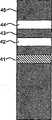
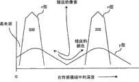
按波长对光子进行的选择性吸收决定了三个光电二极管的光子响应。如果联系图3中450纳米、550纳米和650纳米的光子曲线来考虑传感器区域的位置(“X01+X04”,“X05+X02+X06”,“X07+X03+X08”),则会看到传感器区域的深度和范围决定了光谱响应。在“X01+X04”区域中,与入射的绿光和红光相比,有多出许多的蓝色入射光被吸收,只有少量的绿光和红光被吸收。在“X01+X04”区域中,被吸收的绿色入射光比蓝色入射光要少许多,并且被吸收的绿色入射光比红色入射光要多出许多。在“X05+X02+X06”区域中,被吸收的绿色入射光比蓝色入射光要多(因为入射到区域“X01+X04”的蓝光大部分都被该区域吸收了,而没有到达区域“X05+X02+X06”),并且被吸收的绿色入射光比红色入射光要多(即使入射到区域“X01+X04”的红光只有很少量被该区域吸收,大部分红光会到达区域“X05+X02+X06”)。Selective absorption of photons by wavelength determines the photon response of the three photodiodes. If we consider the location of the sensor regions ("X01+X04", "X05+X02+X06", "X07+X03+X08") in relation to the photon curves at 450nm, 550nm and 650nm in Figure 3, we see The depth and extent of the sensor field determine the spectral response. In the "X01+X04" region, compared with the incident green and red light, much more blue incident light is absorbed, and only a small amount of green and red light is absorbed. In the "X01+X04" region, much less green incident light is absorbed than blue incident light, and much more green incident light is absorbed than red incident light. In the "X05+X02+X06" region, more green incident light is absorbed than the blue incident light (because most of the blue light incident to the region "X01+X04" is absorbed by this region and does not reach the region " X05+X02+X06"), and more green incident light is absorbed than red incident light (even if only a small amount of red light incident on area "X01+X04" is absorbed by this area, most of the red light will reach the area "X05+X02+X06").
入射波长的全部范围(不仅是450纳米、550纳米和650纳米这三个波长)决定了图2所示的三个光电二极管的光谱响应,这与图4所示的很相似。图4中的曲线C1是与图2所示的顶部(“蓝光”)光电二极管相似的顶部(“蓝光”)光电二极管的光谱响应,图4中的曲线C2是与图2所示的中间(“绿光”)光电二极管相似的中间(“绿光”)光电二极管的光谱响应,而图4中的曲线C3是与图2所示的底部(“红光”)光电二极管相似的底部(“红光”)光电二极管的光谱响应。The full range of incident wavelengths (not just the three wavelengths of 450nm, 550nm, and 650nm) determines the spectral response of the three photodiodes shown in Figure 2, which is very similar to that shown in Figure 4. Curve C1 in Figure 4 is the spectral response of a top ("blue") photodiode similar to the top ("blue") photodiode shown in Figure 2, and curve C2 in Figure 4 is the same as the middle ("blue") photodiode shown in Figure 2. The "green") photodiode is similar to the spectral response of the middle ("green") photodiode, while curve C3 in Figure 4 is a bottom ("red") photodiode similar to that shown in Figure 2. Red light") spectral response of the photodiode.
在一类重要的实施例(包括图2所示的VCF传感器组)中,本发明的VCF传感器组实现了三个光电二极管。这种VCF传感器组可很好地适用于DSC或数字摄像机。然而,在其它实施例中,本发明的VCF传感器组实现了两个(或不止三个)光电二极管,它们位于至少主要由半导体材料构成的一体积之内不同的深度。In an important class of embodiments, including the VCF sensor group shown in Figure 2, the VCF sensor group of the present invention implements three photodiodes. This VCF sensor set is well suited for DSC or digital video cameras. However, in other embodiments, the VCF sensor group of the present invention implements two (or more than three) photodiodes located at different depths within a volume at least primarily composed of semiconductor material.
注意到,其吸光率随波长而变化的材料会根据进入该材料的深度而改变穿过该材料而传播的辐射的光谱内容。这种材料在VCF传感器组中可以具有多种功能:它们可以充当滤光片,也可以充当传感器(或传感器的单元)。例如,在图2的实施例中,各个硅区域X01、X02、X03、X09、X10和X11既充当滤光片,也充当至少一个传感器的单元。在其它实施例中,其它半导体(或至少两种不同的半导电材料的层)相似地既充当传感器(或传感器的单元)又充当滤光片。Note that a material whose absorbance varies with wavelength will change the spectral content of radiation propagating through the material depending on the depth into the material. Such materials can have multiple functions in VCF sensor groups: they can act as filters, but also as sensors (or cells of sensors). For example, in the embodiment of FIG. 2 , each silicon region X01 , X02 , X03 , X09 , X10 , and X11 serves both as a filter and as a unit of at least one sensor. In other embodiments, other semiconductors (or layers of at least two different semiconducting materials) similarly function as both sensors (or cells of sensors) and filters.
在一类实施例中,本发明的垂直滤色片(“VCF”)传感器组包括垂直堆叠的传感器,这些传感器包括一个具有顶部表面的顶部传感器,要被检测的辐射入射到顶部表面上并在到达该组的其它任何传感器之前先通过该顶部表面传播到该顶部传感器。该顶部表面定义了法线轴(并且通常至少大体上是平的)。较佳地,这些传感器被配置成当沿该组的垂直轴(上文定义过)传播的辐射入射到该组时,该辐射以相对于法线轴小于约30度的入射角入射到该顶部传感器上。In one class of embodiments, the vertical color filter ("VCF") sensor stacks of the present invention include vertically stacked sensors including a top sensor having a top surface upon which radiation to be detected is incident and Propagates through the top surface to the top sensor before reaching any other sensors of the group. This top surface defines a normal axis (and is usually at least substantially flat). Preferably, the sensors are configured such that when radiation propagating along a vertical axis (defined above) of the group is incident on the group, the radiation strikes the top sensor at an angle of incidence relative to the normal axis of less than about 30 degrees superior.
接下来,参照图5、6和7,将描述除硅以外的半导体材料(例如,InGaN或其它III-V族半导体材料,或除硅以外又不是III-V族材料的半导体材料)被用于形成VCF传感器组的实施例。一种既不是硅又不是III-V族材料的半导体材料是碳化硅。图5是一种VCF传感器组(在垂直平面中)的简化横截面图,它包括顶部传感器10、底部传感器14以及定位于传感器10和14之间的中间传感器12。传感器10和12都由InxGa1-xN半导体材料组成,其中对于传感器10,x=0.475,而对于传感器12,x=0.825。传感器14基本上由硅组成。通常,传感器10和12都由多层InxGa1-xN半导体组成,它们决定了在操作过程中被加上偏压以充当光电二极管的至少一个结,而传感器14由多层具有不同掺杂的硅组成(例如,一层n型硅以及在该n型层上面和下面分别相邻的p型硅层部分),它们在操作过程中被加上偏压以充当光电二极管。Next, referring to FIGS. 5, 6 and 7, it will be described that semiconductor materials other than silicon (for example, InGaN or other III-V group semiconductor materials, or semiconductor materials other than silicon and not III-V group materials) are used for An embodiment of a VCF sensor group is formed. One semiconductor material that is neither silicon nor a III-V material is silicon carbide. FIG. 5 is a simplified cross-sectional view (in the vertical plane) of a VCF sensor group comprising
使用主要由一种或多种III-V族半导体材料组成的晶体管并确定在操作过程中被加上偏压以充当光电二极管的结(任何类型的结,包括异质结或肖特基阻挡层)等做法都落在本发明的范围之内。Use transistors consisting primarily of one or more III-V semiconductor materials and determine the junction (any type of junction, including heterojunction or Schottky barrier) that is biased during operation to act as a photodiode ) etc. all fall within the scope of the present invention.
图6是一张表格,它(在标有“能隙”的中间一栏中)以电子伏特为单位列出了其中铟含量不同的InxGa1-xN半导体(下标“x”的值不同)的带隙能量。图6也(在右边一栏中)列出了与各个带隙能量相对应的光波长。因此,图6指出,由In0.1Ga0.9N半导体制成的传感器所能吸收的最大波长是388纳米,图5所示的传感器10(由In0.475Ga0.525N半导体制成)所能吸收的最大波长约为500纳米,图5所示的传感器12(由In0.825Ga0.175N半导体制成)所能吸收的最大波长约为612纳米。Figure 6 is a table which (in the middle column labeled "Energy Gap") lists Inx Ga1-x N semiconductors (subscript "x" with different indium contents) in electron volts. different values) of the bandgap energy. Figure 6 also lists (in the right column) the wavelengths of light corresponding to the respective bandgap energies. Therefore, Fig. 6 indicates that the sensor made of In0.1 Ga0.9 N semiconductor can absorb the maximum wavelength of 388 nm, and the
因此,传感器10使入射到其上的所有(或基本上所有的)绿光和红光都透射过去,并且最好具有足够的厚度使其能够吸收掉入射到图5所示传感器组上的所有(或基本上所有的)蓝光。相似的是,传感器12使入射到其上的所有(或基本上所有的)红光都透射过去,并且最好具有足够的厚度使其能够吸收掉入射到图5所示传感器组上的所有(或基本上所有的)绿光。传感器14最好具有足够的厚度使其能够吸收掉入射到其上的所有(或至少大部分的)红光。Accordingly,
通常,当使用InxGa1-xN半导体材料(或其它III-V族半导体材料)来形成VCF传感器组时,针对VCF传感器组的各个传感器来选择该材料的参数(比如,InxGa1-xN中的参数“x”)以实现期望的带隙能量(例如,使一个传感器对波长大于阈值的光透明,其中该阈值由带隙能量决定)。Typically, when a VCF sensorgroup is formed using anInxGa1-xN semiconductor material (or other III-V semiconductor material), the parameters of the material (e.g.,InxGa1-x parameter "x" in N) to achieve the desired bandgap energy (eg, to make a sensor transparent to light with wavelengths greater than a threshold, where the threshold is determined by the bandgap energy).
更常见的情况是,在本发明的一些较佳实施例中,除硅以外至少还有一种半导体材料被用于实现VCF传感器组的至少一个传感器,并且选择该材料可使该组中不同的传感器选择性地对不同的波带灵敏。在一些这样的较佳实施例中,使用了至少两种不同类型的半导体材料来实现VCF传感器组中的各个传感器,并且选择材料以使该组中不同的传感器选择性地对不同的波带灵敏。More generally, in some preferred embodiments of the present invention, at least one semiconductor material other than silicon is used to implement at least one sensor of a VCF sensor group, and the material is chosen to make the different sensors in the group Selectively sensitive to different wavebands. In some such preferred embodiments, at least two different types of semiconductor materials are used to implement the individual sensors in the VCF sensor set, and the materials are selected so that the different sensors in the set are selectively sensitive to different wavebands. .
本发明的VCF传感器组的一些实施例包括至少一个“雪崩”光电二极管,这种光电二极管因“雪崩”增益过程而实现每吸收一个光子便可收集不止一个电子。在雪崩增益过程中,通过光子的吸收而产生的第一个电子空穴对产生了至少一个附加的电子空穴对,前提假设是该第一个电子空穴对中电子的能量超过了用于形成光电二极管传感器的半导体材料的带隙能量。半导体材料具有电子电离系数(an)和空穴电离系数(ap),其中1/an是电子在材料中被加速后因碰撞电离而产生新的电子空穴对之前所行进的平均距离,1/ap是空穴在材料中被加速后因碰撞电离而产生新的电子空穴对之前所行进的平均距离。与形成光电二极管的半导体材料中电离系数比ap/an远大于1或远小于1的情况相比,当在形成光电二极管的半导体材料中电离系数比ap/an几乎等于1时,实现实用的雪崩光电二极管将变得非常困难。Some embodiments of the VCF sensor group of the present invention include at least one "avalanche" photodiode that collects more than one electron per absorbed photon due to the "avalanche" gain process. During avalanche gain, at least one additional electron-hole pair is generated by the first electron-hole pair generated by the absorption of a photon, provided that the energy of the electron in this first electron-hole pair exceeds that used for The bandgap energy of the semiconductor material that forms the photodiode sensor. Semiconductor materials have an electron ionization coefficient (an ) and a hole ionization coefficient (ap ), where 1/an is the average distance traveled by an electron after being accelerated in the material before creating a new electron-hole pair due to impact ionization , 1/ap is the average distance traveled by holes before new electron-hole pairs are generated due to impact ionization after being accelerated in the material. When the ionization coefficient ratio ap /an is almost equal to 1 in the semiconductor material forming the photodiode, compared to the case where the ionization coefficient ratio ap /an is much larger than 1 or much smaller than 1 in the semiconductor material forming the photodiode, Realizing a practical avalanche photodiode will become very difficult.
在本发明的一些实施例中,VCF传感器组的至少一个传感器是雪崩传感器,它包括光吸收区域以及和该光吸收区域分开的雪崩区域。例如,图7是可以被包括在VCF传感器组中的这样一个雪崩传感器的横截面图。图7的传感器包括:基片20(由n+型硅制成);基片20上的层21(由n-型硅制成);层21上的层22(由掺杂浓度相对较低的n型InxGa1-xN半导体材料制成);以及层22上的层23(由掺杂浓度相对较高的p型InxGa1-xN半导体材料制成)。金属接点27形成于层23上,基片20通过由n+型硅构成的垂直定向接触区域而耦合到金属接点25。在操作过程中,在金属接点25和27之间加偏压,读出电路可以耦合到接点27。隔离是由层21、22和23周围的电介质材料27A(它可以由光刻胶构成,例如聚甲基戊二酰亚胺保护层)以及层21、22、23和电介质材料27A之间的(以及基片20和材料27A之间的)电介质材料24(可以是氮化硅)来提供的。In some embodiments of the invention, at least one sensor of the VCF sensor group is an avalanche sensor comprising a light absorbing region and an avalanche region separate from the light absorbing region. For example, Figure 7 is a cross-sectional view of such an avalanche sensor that may be included in a VCF sensor set. The sensor of Fig. 7 comprises: substrate 20 (made by n+ type silicon); Layer 21 (made by n-type silicon) on substrate 20; Layer 22 on layer 21 (made by relatively low doping concentration n-type Inx Ga1-x N semiconductor material); and layer 23 on layer 22 (made of p-type Inx Ga1-x N semiconductor material with relatively high doping concentration). Metal contact 27 is formed on layer 23, and substrate 20 is coupled to metal contact 25 through a vertically oriented contact region composed of n+ type silicon. During operation, a voltage bias is applied between metal contacts 25 and 27, to which a readout circuit may be coupled. Isolation is provided by dielectric material 27A around layers 21, 22, and 23 (which may consist of photoresist, such as polymethylglutarimide protective layers) and between layers 21, 22, 23 and dielectric material 27A ( And the dielectric material 24 (which may be silicon nitride) between the substrate 20 and the material 27A is provided.
在操作过程中,层22和23充当光吸收区域,其中响应于入射的光子而形成电子空穴对。用于形成层22和23的InxGa1-xN半导体材料具有远大于(或远小于)1的电离系数比(ap/an),因此层22和23不被用于雪崩增益区域。During operation, layers 22 and 23 act as light absorbing regions where electron-hole pairs are formed in response to incident photons. TheInxGa1- xN semiconductor material used to form layers 22 and 23 has an ionization coefficient ratio (ap /an ) much greater (or much less) than 1, so layers 22 and 23 are not used for the avalanche gain region .
在操作过程中,层21和20充当雪崩增益区域,其中响应于光吸收区域中所形成的电子空穴对而形成了新的电子空穴对。与层22、23的电离系数比相比,用于形成层21和20的硅具有更接近1的电离系数比(ap/an)。During operation, layers 21 and 20 act as avalanche gain regions where new electron-hole pairs are formed in response to electron-hole pairs formed in the light-absorbing region. The silicon used to form layers 21 and 20 has an ionization coefficient ratio (ap /an ) closer to 1 than that of layers 22 , 23 .
通常,本发明的VCF传感器组的一些实施例包括至少一个作为雪崩光电二极管的传感器,其中该雪崩光电二极管包括:光吸收区域,在构成该区域的半导体材料(例如,InGaN)中电子的电离系数与空穴的电离系数相差很大;以及与光吸收区域分开的雪崩区域,在构成该区域的另一种半导体材料(例如,硅)中电子和空穴的电离系数几乎相等。可以预期,作为雪崩光电二极管而实现的传感器的一种重要的用途是检测低强度的辐射,比如,在到达雪崩光电二极管之前通过至少一个滤光片和/或至少一个其它的传感器传播期间其强度已显著减小(例如通过吸收)的辐射。In general, some embodiments of the VCF sensor group of the present invention include at least one sensor that is an avalanche photodiode, wherein the avalanche photodiode includes a light absorbing region, the ionization coefficient of electrons in the semiconductor material (e.g., InGaN) making up the region and an avalanche region, separated from the light-absorbing region, where the ionization coefficients of electrons and holes are nearly equal in another semiconductor material (for example, silicon) constituting the region. It is contemplated that one important use of sensors implemented as avalanche photodiodes is to detect radiation of low intensity, e.g., during propagation through at least one optical filter and/or at least one other sensor before reaching the avalanche photodiode Radiation that has been significantly reduced (for example by absorption).
在本发明的VCF传感器组的其它实施例中,不充当传感器(或传感器单元)的至少一个滤光片与充当传感器(或传感器单元或者一个或多个传感器)的至少一层半导体材料堆叠在一起。这种滤光片可以但并不需要具有与图2所示实施例中的硅相同的光谱灵敏度。In other embodiments of the VCF sensor group of the present invention, at least one optical filter that does not function as a sensor (or sensor unit) is stacked with at least one layer of semiconductor material that functions as a sensor (or sensor unit or one or more sensors) . Such a filter may, but need not, have the same spectral sensitivity as silicon in the embodiment shown in FIG. 2 .
滤光片一般在下述意义上从辐射中除去波长。对于每一个滤光片,都有第一和第二波长,使得如果该第一和第二波长分别以强度“I1”和“I2”入射到滤光片上并且第一和第二波长的透射强度(在通过滤光片透射之后)分别是“O1”和“O2”,则O1≤I1,O2≤I2,并且O1/02<I1/I2。Filters generally remove wavelengths from radiation in the following sense. For each filter, there are first and second wavelengths such that if the first and second wavelengths are incident on the filter with intensities "I1" and "I2" respectively and the transmission of the first and second wavelengths The intensities (after transmission through the filter) are "O1" and "O2", respectively, then O1≤I1, O2≤I2, and O1/02<I1/I2.
本发明的VCF传感器组的一些实施例中所包括的一种类型的滤光片是“转换滤光片”(例如“转换层”),它可以改变入射到其上的电磁辐射的波长。“转换”滤光片吸收一种波长的光子,并发出至少一种波长更短或更长的光子。通常,包括转换滤光片的材料是非线性光学材料。转换滤光片可用于将频率低于传感器截止频率的光子转换为更高的频率,这样它们就可以被检测到了。或者,转换滤光片可用于将频率在阈值频率之上的光子转换到更低的频率,这样它们就可以被检测到了。后者的一个示例是X射线转换层,用于将容易穿透大多数检测材料的X射线转换为易被检测的可见光。在本发明的一些实施例中,厚度约为100微米的氧硫化钆层或厚度约为100微米到600微米的掺有铊的碘化铯层都可以用作这种X射线转换层。One type of filter included in some embodiments of the VCF sensor array of the present invention is a "converting filter" (eg, a "converting layer") that can change the wavelength of electromagnetic radiation incident thereon. A "conversion" filter absorbs photons of one wavelength and emits photons of at least one shorter or longer wavelength. Typically, the material comprising the conversion filter is a nonlinear optical material. Conversion filters can be used to convert photons with frequencies below the sensor's cutoff frequency to higher frequencies so they can be detected. Alternatively, conversion filters can be used to convert photons with frequencies above the threshold frequency to lower frequencies so that they can be detected. An example of the latter is an X-ray conversion layer used to convert X-rays, which readily penetrate most detection materials, into visible light, which is easily detected. In some embodiments of the present invention, a layer of gadolinium oxysulfide having a thickness of about 100 microns or a layer of thallium-doped cesium iodide having a thickness of about 100 to 600 microns can be used as such an X-ray conversion layer.
有两种相关的方式来检测一组光谱带中的光子,并且每一种方式都可以用于实现本发明。在本发明的VCF传感器组的一些实施例中,至少一个滤光片除去至少一个波带以外的光子,并且至少两个垂直堆叠的传感器检测剩余的光子,其中每一个传感器都是与每一个滤光片分离的元件。本发明的VCF传感器组的其它实施例并不包括非传感器滤光片(即不是传感器的滤光片),但确实包括对有限的波带灵敏的传感器。本发明的其它实施例可以通过包括第一传感器和在第一传感器下面的第二传感器,来实现这些方法的组合,其中第一传感器吸收了有限范围的波长并使该范围以外的光子透射到第二传感器,并且该第二传感器对所有的波长都灵敏。在本示例中,第一传感器充当第二传感器的滤光片。There are two related ways to detect photons in a set of spectral bands, and either way can be used to implement the invention. In some embodiments of the VCF sensor array of the present invention, at least one filter removes photons outside at least one wavelength band, and at least two vertically stacked sensors detect the remaining photons, each of which is connected to each filter. Components for light sheet separation. Other embodiments of the VCF sensor group of the present invention do not include non-sensor filters (ie, filters that are not sensors), but do include sensors sensitive to a limited waveband. Other embodiments of the invention may implement a combination of these methods by including a first sensor and a second sensor below the first sensor, wherein the first sensor absorbs a limited range of wavelengths and transmits photons outside this range to the second sensor. two sensors, and the second sensor is sensitive to all wavelengths. In this example, the first sensor acts as a filter for the second sensor.
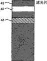
在本发明的一些实施例中,至少一个非传感器滤光片定位于VCF传感器组中的至少一对垂直堆叠的传感器之间,或该组的顶部传感器之上,或该组的底部传感器之下。当这种滤光片定位于VCF传感器组中的一对垂直堆叠的传感器之间时,该滤光片可以是多种不同类型中的任一种,这包括(但不限于下面这些):滤光片可以吸收一个波带中的辐射并且透射其它波长而同时不对任何波长的辐射造成太多的反射;滤光片可以反射一个波带中的辐射并且透射其它波长而同时不对任何波长的辐射造成太多的吸收;或滤光片可以对一个波带中的辐射高度透射,对另一个波带中的辐射高度吸收,并且对第三个波带中的辐射造成高度反射。图8的VCF传感器组包括两个后一种类型的非传感器滤光片:滤色片43和滤色片48。应该理解,图8所示的传感器组只是本发明可预计的许多实施例中的一个示例。In some embodiments of the invention, at least one non-sensor filter is positioned between at least one pair of vertically stacked sensors in a VCF sensor group, or above the top sensor of the group, or below the bottom sensor of the group . When such a filter is positioned between a pair of vertically stacked sensors in a VCF sensor stack, the filter can be any of a number of different types, including (but not limited to) the following: An optical sheet can absorb radiation in one waveband and transmit other wavelengths without causing too much reflection to any wavelength; a filter can reflect radiation in one waveband and transmit other wavelengths without causing too much reflection to any wavelength Too much absorption; or the filter can be highly transmissive to radiation in one band, highly absorbent in another, and highly reflective in a third. The VCF sensor group of FIG. 8 includes two non-sensor filters of the latter type:
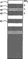
图8是本发明的VCF传感器组阵列的一个实施例(在垂直平面中)的部分截面图,它包括两个非传感器滤光片(层43和48)以及四个绝缘层(扩散阻挡层42、44、47和48)。每一个绝缘层可以由二氧化硅构成。在图8中,一个VCF传感器组包括:层51(由n型半导体制成)以及在层51上面和下面的p型半导体材料层50;在材料50下面的绝缘层49;在层49下面的滤色片48;在滤光片48下面的绝缘层47;层46(由n型半导体制成)以及在层46上面和下面的p型半导体材料层45;在材料45下面的绝缘层44;在层44下面的滤色片43;在滤光片43下面的绝缘层42;层41(由n型半导体制成)以及在层41上面和下面的p型半导体基片材料40。垂直定位的插头将层41、46和51都连接到传感器组的顶部表面,这样各个层41、46和51都可以耦合到偏压和读出电路。遮光板54安装在插头上面以防止辐射(正入射到传感器组顶部表面的辐射)到达插头而减弱频率选择性。图8的阵列也包括第二VCF传感器组,它包括:层63(由n型半导体制成)以及在层63上面和下面的p型半导体材料层50;在材料50下面的绝缘层49;在层49下面的滤色片48;在滤光片48下面的绝缘层47;层62(由n型半导体制成)以及在层62上面和下面的p型半导体材料层45;在材料45下面的绝缘层44;在层44下面的滤色片43;在滤光片43下面的绝缘层42;层61(由n型半导体制成)以及在层61上面和下面的p型半导体基片材料40。垂直定位的插头将层61、62和63都连接到传感器组的顶部表面,这样各个层61、62和63都可以耦合到偏压和读出电路。遮光板53安装在第二VCF传感器组的插头上面以防止辐射(正入射到传感器组顶部表面的辐射)到达插头。8 is a partial cross-sectional view (in the vertical plane) of one embodiment (in the vertical plane) of a VCF sensor group array of the present invention, which includes two non-sensor filters (layers 43 and 48) and four insulating layers (diffusion barrier layer 42). , 44, 47 and 48). Each insulating layer may consist of silicon dioxide. In FIG. 8, a VCF sensor group includes: layer 51 (made of n-type semiconductor) and
在图8所示实施例的变体中,n型层51和63的水平定向变体(它们缺少垂直定向的接触部分)暴露于传感器组的顶部表面(并且并不被半导体材料50覆盖)。每一个这样暴露的n型层可以直接连接到(例如,通过形成于其上的金属接触)偏压和读出电路。相似的是,在图8所示实施例的变体中,n型层46和62直接置于层47下面(不再用p型半导体材料45将其与层47分离),n型层41和61直接置于层42下面(不再用p型半导体材料40将其与层42分离)。In a variation of the embodiment shown in Figure 8, horizontally oriented variants of n-
在操作过程中,使图8中的每一层p型半导体层都保持地面电势。通过可接入(或可耦合到)偏压和读出电路的插头而将每一层n型层都耦合起来。在每一个传感器组的每一次读出之前,偏压电路将每一层n型层复位到基准电势(在地面电势之上)。在暴露于要检测的辐射期间,第一传感器组中相邻的p型和n型层配对后反向偏压便可充当光电二极管:第一光电二极管,其阴极是层51,其阳极是相邻的材料层50(被称为“蓝光”传感器,因为它响应于入射到该传感器组顶部的白光而吸收了比绿光或红光光子要多的蓝光光子);第二光电二极管,其阴极是层46,其阳极是相邻的材料层45(被称为“绿光”传感器,因为当白光入射到该传感器组顶部时它吸收了比蓝光或红光光子要多的绿光光子);以及第三光电二极管,其阴极是层41,其阳极是相邻的材料层40(被称为“红光”传感器,因为当白光入射到该传感器组顶部时它吸收了比蓝光或绿光光子要多的红光光子)。在暴露于要检测的辐射期间,第二传感器组中相邻的p型和n型层配对后反向偏压便可充当光电二极管:第一光电二极管,其阴极是层63,其阳极是相邻的材料层50(被称为“蓝光”传感器,因为它响应于入射到该第二传感器组顶部的白光而吸收了比绿光或红光光子要多的蓝光光子);第二光电二极管,其阴极是层62,其阳极是相邻的材料层45(被称为“绿光”传感器,因为当白光入射到该第二传感器组顶部时它吸收了比蓝光或红光光子要多的绿光光子);以及第三光电二极管,其阴极是层61,其阳极是相邻的材料层40(被称为“红光”传感器,因为当白光入射到该第二传感器组顶部时它吸收了比蓝光或绿光光子要多的红光光子)。During operation, each p-type semiconductor layer in FIG. 8 is maintained at ground potential. Each n-type layer is coupled through plugs that are accessible to (or coupleable to) biasing and readout circuitry. A bias circuit resets each n-type layer to a reference potential (above ground potential) prior to each readout of each sensor group. During exposure to the radiation to be detected, adjacent p-type and n-type layers in the first sensor group are paired and reverse-biased to act as photodiodes: a first photodiode whose cathode is
当层40、41、45、46、50和51由结晶硅制成时(通常都是这样),层51和50最好分别比层46和45要薄并且层41和40分别比层51和50要薄,厚度的差值要足以确保入射到各绿光传感器的绿光和红光的强度比足够得高,同时确保比绿光多得多的红光入射到各红光传感器上并且比绿光多得多的蓝光被各蓝光传感器吸收。通常,第一传感器组中的层51和50(以及第二传感器组中的层63和50)组合厚度是0.3微米或更少,并且第一传感器组中的层45和46(以及第二传感器组中的层45和62)组合厚度约为0.5微米。When layers 40, 41, 45, 46, 50, and 51 are made of crystalline silicon (which is usually the case), layers 51 and 50 are preferably thinner than
滤色片43是“红光通过/青光反射”滤光片,它对红光高度透射但反射入射于其上的大部分或几乎全部的蓝光和绿光。滤色片48是“黄光通过/蓝光反射”滤光片,它对入射于其上的红光和绿光高度透射,但反射入射于其上的大部分或几乎全部的蓝光。本发明的其它实施例使用非反射型的透射滤光片。
滤光片43的作用在于增大由各个红光传感器所吸收的红光和绿光的比(以及红光和蓝光的比),并且可以减小或消除若省去滤光片43则可能影响红光传感器的红/绿区分问题。相似的是,滤光片48的作用在于增大由各个绿光传感器所吸收的绿光和蓝光的比,并且可以减小或消除若省去滤光片48则可能影响绿光传感器的绿/蓝区分问题。The effect of
滤光片48的作用还在于增大由各个蓝光传感器所吸收的蓝光和绿光(以及红光)的比,因为从滤光片48反射的蓝光有另一次机会被蓝光传感器吸收。各个蓝光传感器的蓝光吸收都得到提高,而同时不增大其对红光和绿光的响应,因为并没有多少红光和绿光从滤光片48反射回蓝光传感器。相似的是,滤光片43的作用还在于增大由各个绿光传感器所吸收的绿光和红光的比,因为从滤光片43反射的绿光有另一次机会被绿光传感器吸收。各个绿光传感器的绿光吸收都有所提高,而同时不增大其对红光的响应,因为并没有多少红光从滤光片43反射回绿光传感器。非常少的蓝光到达绿光传感器,因为几乎所有的蓝光要么被蓝光传感器吸收了,要么被滤光片48朝着蓝光传感器反射回去了。
有种类多样的材料都可以充当VCF传感器组中的滤光片(例如,图8中的滤光片43或48,或反射一个波带而对所有其它波长均透射的滤光片,或吸收一个波带但并不反射的滤光片)。这些材料可以组合使用或具有各种厚度。这些配置部分程度上由它们的光学特性确定,但主要取决于加工集成因素。A wide variety of materials can act as filters in a VCF sensor group (e.g., filters 43 or 48 in Figure 8, or filters that reflect one wavelength band and transmit all others, or absorb one band but not reflective filter). These materials can be used in combination or have various thicknesses. These configurations are determined in part by their optical properties, but mainly by process integration factors.
材料以及材料之间的界面可以反射光子。当镜子的反射率按波长具有选择性时,该镜子(无论是材料还是材料之间的界面)可以充当本发明的VCF传感器组中的滤光片。例如,本发明的VCF传感器组的一些实施例包括分色镜,它透射第一波带中的辐射而反射第二波带中的辐射。Materials and interfaces between materials can reflect photons. When the reflectivity of the mirror is wavelength-selective, the mirror (whether it is a material or an interface between materials) can act as a filter in the VCF sensor group of the present invention. For example, some embodiments of the inventive VCF sensor group include a dichroic mirror that transmits radiation in a first waveband and reflects radiation in a second waveband.
如上所述,由光吸收随波长而变化的材料制成的堆叠层可以被用作本发明的VCF传感器组的各个实施例中的滤光片。在包括不同掺杂半导体材料(例如硅)层的较佳实施例中,至少一层半导体层被同时用作滤光片和传感器。在一层半导体材料被同时用作滤光片和光电二极管传感器的阴极(或阳极)的VCF传感器组中,可以通过控制加在光电二极管的阳极和阴极之间的偏压,也可以通过确定掺杂原子的掺杂水平和位置以及传感器单元的结构间隔,来适当控制该传感器的光谱灵敏度。As noted above, stacked layers of materials whose light absorption varies with wavelength may be used as optical filters in various embodiments of the VCF sensor group of the present invention. In a preferred embodiment comprising layers of a differently doped semiconductor material (eg silicon), at least one semiconductor layer is used both as a filter and as a sensor. In the VCF sensor group in which a layer of semiconductor material is used as both the filter and the cathode (or anode) of the photodiode sensor, the bias voltage applied between the anode and cathode of the photodiode can be controlled, and the doped The doping level and position of the heteroatoms and the structural spacing of the sensor units are used to properly control the spectral sensitivity of the sensor.
被包括在本发明的一些实施例中的另一种类型的滤光片是薄金属膜。薄金属膜可以充当部分反射器,由此可以过滤入射的光子。被反射的光子通过它们上面的各个层而返回,这给了它们第二次被吸收的机会。Another type of filter included in some embodiments of the present invention is a thin metal film. Thin metal films can act as partial reflectors, thereby filtering incoming photons. The reflected photons travel back through the layers above them, giving them a second chance to be absorbed.
本发明的一些实施例中所包括的其它类型的滤光片是:干涉滤光片(例如,具有不同介电常数的电介质材料的堆叠层),它反射某些波长并使其它波长通过;以及有机、无机染料和色素。Other types of filters included in some embodiments of the invention are: interference filters (e.g., stacked layers of dielectric materials with different dielectric constants), which reflect certain wavelengths and pass others; and Organic and inorganic dyes and pigments.
在本发明的一些实施例中,滤光片以任一种图案分布在阵列的VCF传感器组中,例如,像申请号为10/103,304的专利中所描述的那样。这些滤光片可以但并不需要全部都完全相同。较佳地,每一个滤光片与VCF传感器组之一形成一体(例如,作为形成于半导体层上或半导体层之间的一个层)。或者,滤光片和传感器组可以单独制造,然后将滤光片定位于该传感器组阵列上并与VCF传感器组接合(或附着于或固定到相对于VCF传感器组的一个固定位置处)。滤光片可以按图8A所示的“交替”方式或“棋盘”方式来设置,其中标有“RGB”的每一个正方形表示VCF传感器组,并且标有“X”的每一个正方形表示包括一个滤光片的VCF传感器组。如图8A所示,每一个奇数号的行中的每一个奇数号传感器组包括一个滤光片,每一个偶数号行中的每一个偶数号传感器组包括一个滤光片,由此在具有滤光片的彩色传感器组和不具有滤光片的彩色传感器组之间获得了最佳的空间频率。In some embodiments of the invention, the filters are distributed in any pattern among the VCF sensor groups of the array, for example, as described in application Ser. No. 10/103,304. These filters can, but need not all be identical. Preferably, each filter is integral with one of the VCF sensor groups (eg, as a layer formed on or between semiconductor layers). Alternatively, the filter and sensor pack can be manufactured separately, and the filter then positioned on the sensor pack array and engaged with the VCF sensor pack (or attached or fixed at a fixed position relative to the VCF sensor pack). The filters can be arranged in an "alternating" pattern or a "checkerboard" pattern as shown in Figure 8A, where each square labeled "RGB" represents a set of VCF sensors, and each square labeled "X" represents a group comprising a Filter VCF sensor set. As shown in Fig. 8A, each odd-numbered sensor group in each odd-numbered row includes an optical filter, and each even-numbered sensor group in each even-numbered row includes an optical filter, thereby having a filter The best spatial frequency was obtained between the color sensor group with the light sheet and the color sensor group without the filter.
或者,滤光片可以按图8B所示的图案来设置,其中标有“RGB”的每一个正方形表示VCF传感器组,标有“X”的每一个正方形表示包括一个滤光片的VCF传感器组。当滤光片按图8B所示图案来设置时,按一种同时允许满测度彩色读出和马赛克仿真读出的方式来分配滤光片,同时确保两种类型的图像读出包含彩色传感器组输出和滤色片的每一种组合。或者,可以按任何其它图案在VCF传感器组阵列的传感器组中分配滤光片,其中的某些在申请号为10/103,304的专利中有所描述。Alternatively, the filters can be arranged in the pattern shown in Figure 8B, where each square labeled "RGB" represents a VCF sensor group, and each square marked "X" represents a VCF sensor group that includes a filter . When the filters are arranged in the pattern shown in Figure 8B, the filters are distributed in a manner that allows both full-scale color readout and mosaic simulation readout, while ensuring that both types of image readout include color sensor groups Every combination of output and filter. Alternatively, the filters may be distributed among the sensor groups of a VCF sensor group array in any other pattern, some of which are described in Ser. No. 10/103,304.
本发明的VCF传感器组的一些实施例包括至少一个透镜以替代至少一个滤光片或作为该至少一个滤光片的补充。例如,在VCF传感器组阵列中,可以在每一个(或只是一些)VCF传感器组上形成微透镜。有时当金属化(或另一种结构)限制了VCF传感器组的孔径大小(在成像平面中入射辐射将传播到至少一个传感器上的面积)时,光刻胶可以沉积到该孔径上,然后显影,这样光刻胶材料熔化成凹或凸型,从而形成了微透镜。根据构成透镜的材料的特性和透镜形状,透镜除了可以用作透镜以外可以充当滤光片。例如,图9是图8所示VCF传感器组阵列的变体(在垂直平面中)的部分横截面图。图9所示的阵列包括第一VCF传感器组,该第一VCF传感器组进一步包括:n型半导体层51、46和41,它们都形成于p型半导体材料之中;垂直定向的接点,用于将各个层41、46和51连接到传感器组的顶部表面;以及遮光板54,它安装在接点上面以防止辐射(正入射到传感器组的顶部表面上的辐射)到达接点。图9所示阵列还包括第二VCF传感器组,该第二VCF传感器组进一步包括:n型半导体层61、62和63,它们都形成于p型半导体材料之中;垂直定向的接点,用于将各个层61、62和63连接到传感器组的顶部表面;以及遮光板53,它安装在接点上面以防止辐射(正入射到传感器组的顶部表面上的辐射)到达接点。遮光板53和54形成于层64中,而层64对要检测的辐射透明。遮光板53和54围绕着第一传感器组的孔径,并且遮光板53和另一个遮光板(未示出)围绕着第二传感器组的孔径。凸微透镜65形成于第一组的孔径上面的层64之上,凸微透镜66形成于第二组的孔径上面的层64之上。Some embodiments of the VCF sensor group of the present invention include at least one lens instead of or in addition to at least one optical filter. For example, in an array of VCF sensor groups, microlenses can be formed on each (or just some) VCF sensor groups. Sometimes when metallization (or another structure) limits the aperture size (area in the imaging plane where incident radiation will spread onto at least one sensor) of a VCF sensor group, photoresist can be deposited onto this aperture and then developed , so that the photoresist material is melted into a concave or convex shape, thus forming a microlens. Depending on the properties of the material constituting the lens and the shape of the lens, the lens may function as a filter in addition to the lens. For example, FIG. 9 is a partial cross-sectional view (in the vertical plane) of a variation (in the vertical plane) of the VCF sensor group array shown in FIG. 8 . The array shown in FIG. 9 includes a first VCF sensor group further comprising: n-type semiconductor layers 51, 46 and 41 formed in p-type semiconductor material; vertically oriented contacts for The respective layers 41, 46 and 51 are attached to the top surface of the sensor group; and a
当微透镜按交替图案(图8A所示的图案)分布在VCF传感器组阵列的传感器组中时,可以单独选择传感器组中对辐射具有不同灵敏度的各个子集。这为作为一个整体的阵列提供了扩展的动态范围。When the microlenses are distributed in the sensor groups of the VCF sensor group array in an alternating pattern (the pattern shown in FIG. 8A ), each subset of the sensor groups having different sensitivities to radiation can be individually selected. This provides extended dynamic range for the array as a whole.
在VCF传感器组阵列中各个传感器组的孔径通常是正方形或八边形,但也可以具有其它形状(例如,矩形、圆形或不规则形状)。在这种阵列的全部或一些传感器组的孔径上所形成的微透镜通常是正方形的,但也可以具有其它形状。The apertures of the individual sensor groups in a VCF sensor group array are typically square or octagonal, but may also have other shapes (eg, rectangular, circular, or irregular). The microlenses formed over the apertures of all or some of the sensor groups of such an array are typically square, but may have other shapes.
本发明的VCF传感器组的一些实施例包括至少一个作为复合透镜的微透镜(例如,凹微透镜和凸微透镜的组合)。Some embodiments of the VCF sensor group of the present invention include at least one microlens as a composite lens (eg, a combination of a concave microlens and a convex microlens).
众所周知,形成微透镜并以之作为CCD图像传感器阵列的顶层,其中阵列的每一个传感器上有一个微透镜。同时也知道,包括的微透镜可作为CCD图像传感器阵列的中间层,例如,在阵列的每一个传感器上有两个垂直分离的微透镜,并且在这对垂直分离的微透镜之间有滤色片。在本发明的一些实施例中,微透镜(例如,图9的微透镜65)相对于VCF传感器组的传感器而定位,以便将辐射折射到该组的顶部传感器(例如,图9中包括层51的那个传感器)中,使至少一些辐射通过顶部传感器传到位于该顶部传感器下面的各传感器,前提假设是该辐射包括在其可以到达底部传感器之前既不被该组吸收又不被该组的元件所反射的至少一个波长。It is known to form microlenses as the top layer of a CCD image sensor array, one microlens on each sensor of the array. It is also known to include microlenses as interlayers in CCD image sensor arrays, for example, with two vertically separated microlenses on each sensor of the array, and a color filter between the pair of vertically separated microlenses piece. In some embodiments of the invention, a microlens (e.g., microlens 65 of FIG. 9 ) is positioned relative to the sensors of a VCF sensor group so as to refract radiation to the top sensor of the group (e.g.,
在本发明的典型实施例中,非常期望将半导体加工处理过程中(出于其它目的)已经使用过的材料用于实现滤光片、透镜和传感器,因为它们可以在不修改工艺的情况下被添加到VCF传感器组中。这种材料的示例是多晶硅、二氧化硅和氮化硅。多晶硅层可以用作滤光片,其吸收光谱取决于其结晶特性和导电性以及该层的厚度和相对于VCF传感器组其它单元的深度。在某一表面(例如,硅表面)上生长的氧化硅层和二氮化硅层可以形成VCF传感器组中的干涉滤光片。In typical embodiments of the invention, it is highly desirable to use materials already used (for other purposes) in semiconductor processing to implement filters, lenses, and sensors because they can be fabricated without process modification. Added to the VCF sensor group. Examples of such materials are polysilicon, silicon dioxide and silicon nitride. A polysilicon layer can be used as a filter whose absorption spectrum depends on its crystalline properties and conductivity as well as the layer's thickness and depth relative to the other elements of the VCF sensor group. A layer of silicon oxide and silicon nitride grown on a surface (eg, a silicon surface) can form an interference filter in a VCF sensor group.
在本文中,在用来实施本发明的VCF传感器组中,“尺寸最小的”载流子收集单元这样一种表述是指,其在与该组顶部传感器的上表面所定义的法线轴相垂直的一平面上所投影的面积不大于该组其它载流子收集单元在该平面上所投影的面积的那个载流子收集单元。在本文中,(一组的)“最小收集面积”是指,该组中尺寸最小的载流子收集单元在与该组顶部传感器的上表面所定义的法线轴相垂直的一平面上所投影的面积。在本发明的传感器组的一类实施例中,如图10、10A和10B的传感器组中所示,与该组中的每一个尺寸最小的载流子收集单元相比,该组中某一个传感器的载流子收集单元基本上具有更大的“尺寸”(在与该组顶部传感器的上表面的法线轴相垂直的平面上投影的面积)。在这一类较佳实施例中,传感器组的某一个载流子收集单元具有至少两倍于该组最小收集面积的尺寸。该载流子收集单元通常由阵列中的至少一个其它传感器组所共用,并且其尺寸通常至少基本上等于共用它的所有组的尺寸总和。In this context, in the VCF sensor group used to practice the present invention, the expression "smallest" carrier-collecting unit means that it is perpendicular to the normal axis defined by the upper surface of the top sensor of the group. The carrier collection unit whose projected area on a plane is not larger than the projected area of the group of other carrier collection units on the plane. In this context, the "minimum collection area" (of a group) refers to the projection of the smallest carrier collection unit in the group on a plane perpendicular to the normal axis defined by the upper surface of the top sensor in the group. area. In a class of embodiments of the sensor group of the present invention, as shown in the sensor group of FIGS. The carrier collection unit of the sensor basically has a larger "size" (area projected on a plane perpendicular to the normal axis of the upper surface of the set of top sensors). In a preferred embodiment of this type, a certain carrier collection unit of the sensor group has a size at least twice the smallest collection area of the group. The carrier collection unit is typically shared by at least one other sensor group in the array, and its size is usually at least substantially equal to the sum of the sizes of all groups sharing it.
图10的阵列包括多个传感器组,其中六个示出在图10中。每一个传感器组包括一个绿光传感器(其载流子收集区域不与任何其它传感器组共用)、一个蓝光传感器(与一个其它的传感器组共用)以及一个红光传感器(与一个其它的传感器组共用)。每一个红光传感器和蓝光传感器的载流子收集区域都被两个传感器组共用。用于蓝光和红光光子的载流子收集区域大于用于绿光光子的收集区域。The array of FIG. 10 includes multiple sensor groups, six of which are shown in FIG. 10 . Each sensor group includes a green sensor (whose carrier collection area is not shared with any other sensor group), a blue sensor (shared with one other sensor group), and a red sensor (shared with one other sensor group). ). The carrier collection area of each red sensor and blue sensor is shared by both sensor groups. The carrier collection area for blue and red photons is larger than that for green photons.
在图10或10B所示阵列的变体中,至少一个载流子收集区域(由两个传感器组共用)包括两个或多个部分,这些部分最初形成时彼此横向分离,然后将它们短路在一起形成单个有效的载流子收集区域。例如,每一个蓝光传感器可以包括两个横向分离的用于蓝光光子的载流子收集区域,每个区域形成在绿光光子的不同载流子收集区域上,这两个用于蓝光光子的载流子收集区域横向分离,以便在两者之间的阵列上表面上提供形成至少一个晶体管的空间。每一个蓝光传感器的两个横向分离的载流子收集区域被短接在一起,形成单个有效的用于蓝光光子的载流子收集区域,其总尺寸比阵列中每一个用于绿光光子的载流子收集区域都要大。In a variant of the array shown in Figure 10 or 10B, at least one carrier collection region (shared by two sensor groups) consists of two or more sections that are initially formed laterally separated from each other and then short-circuited between the Together form a single effective carrier collection region. For example, each blue light sensor may include two laterally separated carrier collection regions for blue photons, each region formed on a different carrier collection region for green photons, the two carrier collection regions for blue photons The carrier collection regions are separated laterally to provide space for forming at least one transistor on the upper surface of the array therebetween. The two laterally separated carrier-collecting regions of each blue-light sensor are shorted together to form a single effective carrier-collecting region for blue-light photons, whose overall size is larger than that of each for green-light photons in the array. The carrier collection area must be large.
参照图10,每一个红光传感器上所收集的电荷被转换为电信号,该电信号表示共用该红光传感器的两个传感器组上所入射的红光强度的平均值的两倍。每一个蓝光传感器上所收集的电荷被转换为电信号,该电信号表示共用该蓝光传感器的两个传感器组上所入射的蓝光强度的平均值的两倍。这样,该阵列有关绿光的分辨率是有关红光或蓝光的分辨率的两倍。这种类型的阵列增大了蓝光和红光信道中的信噪比,同时还维持了绿光(或像亮度这样的)信道中的高空间分辨率。高亮度分辨率得以实现,因为每一个像素位置都具有有效的绿光传感器,相比之下,使用Bayer图案的常规图像传感器阵列仅在一半的像素位置处具有绿光传感器。本领域的技术人员应该会认识到,通过绿光信道中更高的采样率来保持高亮度分辨率会使采用这种阵列所产生的内插图像中存在的伪像有所减少。更大的蓝光和红光载流子收集区域会进一步减少伪像的存在。Referring to FIG. 10, the charge collected on each red sensor is converted into an electrical signal representing twice the average value of the incident red light intensity on the two sensor groups sharing the red sensor. The charge collected on each blue light sensor is converted into an electrical signal representing twice the average of the incident blue light intensity on the two sensor groups sharing that blue light sensor. Thus, the array has twice the resolution with respect to green light than with respect to red or blue light. This type of array increases the signal-to-noise ratio in the blue and red channels, while also maintaining high spatial resolution in the green (or like luminance) channel. High brightness resolution is achieved because there is an active green sensor at every pixel location, compared to only half of the pixel locations where conventional image sensor arrays using Bayer patterns have green sensors. Those skilled in the art will recognize that maintaining high luminance resolution through higher sampling rates in the green channel will result in less artifacts in interpolated images produced using such an array. Larger blue and red carrier collection areas further reduce artifacts.
在其它实施例中,VCF传感器组阵列中蓝光传感器的载流子收集区域小于该阵列的红光和绿光传感器的载流子收集区域。In other embodiments, the carrier collection area of the blue sensor in the VCF sensor group array is smaller than the carrier collection area of the red and green sensors of the array.
在VCF传感器组阵列的一些实施例中,一个传感器组包括至少一个与另一个传感器组共用的传感器(或传感器的单元)。图10A是这种阵列(在垂直平面中)的横截面图。在图10A中,第一传感器组包括:第一传感器,该第一传感器自身又包括层102(由n型半导体制成)以及紧靠层102上面和下面的p型材料区域100;以及第二传感器,该第二传感器自身又包括层101(由n型半导体制成)以及紧靠层101上面和下面的p型材料区域100。图10A也示出了第二传感器组,它包括:第三传感器(该第三传感器又包括n型半导体制成的层103以及紧靠层103上面和下面的p型材料区域100)和第二传感器。由此,第二传感器(它包括层101)由两个传感器组共用,并且分离的第一和第三传感器定位于该阵列中同一垂直水平处。In some embodiments of an array of VCF sensor groups, one sensor group includes at least one sensor (or unit of sensors) that is shared with another sensor group. Figure 10A is a cross-sectional view (in the vertical plane) of such an array. In FIG. 10A, the first sensor group comprises: a first sensor which itself comprises a layer 102 (made of n-type semiconductor) and a
图10A阵列可以被配置成,第一传感器的输出表示第一像素的蓝光成分,第三传感器的输出表示第二像素的蓝光成分,第二传感器的输出同时表示第一像素和第二像素的绿光成分。图10A所示阵列较佳地可操作于:绿光分辨率好于蓝光的模式(例如,通过单独地使用第一、第二和第三传感器的输出);以及蓝光分辨率与绿光分辨率相同的模式(例如,通过对第一和第三传感器的输出求平均,并且将该平均值与第二传感器的输出一起使用)。图10A所示阵列是只具有两个深度处的传感器的简单实施例。在本发明的阵列的其它实施例中,传感器组都具有垂直排列在三个或更多不同深度的传感器。The array of FIG. 10A can be configured such that the output of the first sensor represents the blue light content of the first pixel, the output of the third sensor represents the blue light content of the second pixel, and the output of the second sensor represents the green color of both the first pixel and the second pixel. light component. The array shown in FIG. 10A is preferably operable: in a mode in which the resolution of green light is better than that of blue light (e.g., by using the outputs of the first, second, and third sensors individually); The same pattern (eg, by averaging the outputs of the first and third sensors, and using that average with the output of the second sensor). The array shown in Figure 10A is a simple embodiment with sensors at only two depths. In other embodiments of the array of the invention, the sensor groups each have sensors vertically arranged at three or more different depths.
在图10B所示的VCF传感器组阵列中,每一个传感器组的红光和蓝光传感器的载流子收集单元具有比该组的绿光传感器的载流子收集单元要大的尺寸。图10B的阵列包括多个传感器组,图10B中示出了其中的四个。每一个传感器组包括:一个绿光传感器,其载流子收集区域(182、183、184或185)并不与任何其它传感器组共用;一个蓝光传感器,其载流子收集区域(180)与三个其它的传感器组共用;以及一个红光传感器,其载流子收集区域(181)与三个其它的传感器组共用。用于蓝光和红光光子的载流子收集区域大于用于绿光光子的收集区域。每一个红光传感器上(因光子吸收)所收集的电荷被转换为电信号(通常是电压),该电信号表示共用该红光传感器的四个传感器组上所入射的红光强度的平均值。每一个蓝光传感器上所收集的电荷被转换为电信号(通常是电压),该电信号表示共用该蓝光传感器的四个传感器组上所入射的蓝光强度的平均值。通常,并不需要相对于绿光传感器的电压输出来标定图10B所示阵列(及其变体)的红光和蓝光传感器的电压输出,因为因传感器中载流子收集区域的增大而导致各传感器上所收集的电荷的增大正比于因这种载流子收集区域的增大而导致的传感器电容的增大。In the VCF sensor group array shown in FIG. 10B , the carrier collection unit of the red and blue sensors of each sensor group has a larger size than the carrier collection unit of the green sensor of the group. The array of Figure 10B includes multiple sensor groups, four of which are shown in Figure 10B. Each sensor group includes: a green light sensor whose carrier collection region (182, 183, 184 or 185) is not shared with any other sensor group; a blue light sensor whose carrier collection region (180) is shared with three and a red light sensor whose carrier collection region (181) is shared with three other sensor groups. The carrier collection area for blue and red photons is larger than that for green photons. The charge collected on each red sensor (due to photon absorption) is converted to an electrical signal (usually a voltage) that represents the average intensity of the incident red light on the four sensor groups that share that red sensor . The charge collected on each blue light sensor is converted into an electrical signal (usually a voltage) representing the average intensity of blue light incident on the four sensor groups sharing that blue light sensor. In general, it is not necessary to scale the voltage output of the red and blue sensors of the array shown in Figure 10B (and its variants) relative to the voltage output of the green sensor because of the increased charge carrier collection area in the sensor. The charge collected on each sensor increases proportional to the increase in sensor capacitance due to this increase in carrier collection area.
当制造VCF传感器组的阵列使得每一个传感器组的输出确定一个像素时,有必要使传感器组彼此隔离以避免像素之间的串扰。如果一个传感器组中所产生的电子和空穴可以漂移到另一个之中,则成像器的分辨率就会下降。在本发明的较佳实施例中,可通过制造其物理设计包含它们内部所产生的电荷的传感器组,便可实现这种隔离。When fabricating an array of VCF sensor groups such that the output of each sensor group determines a pixel, it is necessary to isolate the sensor groups from each other to avoid crosstalk between pixels. If the electrons and holes generated in one sensor group can drift into the other, the resolution of the imager is reduced. In a preferred embodiment of the invention, this isolation is achieved by fabricating sensor groups whose physical design includes their internally generated charges.
例如,参照图10A,在图10A的阵列中,用n-p基片结将下面的那个较大的“第二传感器”(包括层101)与其垂直深度相同的近邻(部分示出,但未标记)隔离开,就像用n-p基片结将较小的“第一”和“第三”传感器(分别包括层102和103)彼此隔离开那样。For example, referring to FIG. 10A, in the array of FIG. 10A, the lower, larger "second sensor" (including layer 101) is connected to its vertically deep neighbor (partially shown, but not labeled) by an n-p substrate junction. are isolated, as are the smaller "first" and "third" sensors (including
一些常规的传感器阵列并不在其输出会确定不同像素的那些传感器之间实现这种隔离。例如,一种类型的常规传感器阵列(图11有示出,在Bartek中的“Sensors and Actuators”A,41-42(1994),pp.123-128中有所描述)包括在外延硅(epi)层(31)中产生的光电二极管传感器(例如,光电二极管30),而这层外延硅为所有像素所共用。在这种配置中,一个传感器中所产生的电荷可以漂移到相邻的传感器中或有可能漂得更远。因为图11中的结构缺少传感器之间的隔离区域(例如,p型半导体区域),所以共用的外延层(层31)提供了一条通道,该通道可以将载流子从一个像素下面传导至另一个像素下面。Some conventional sensor arrays do not implement this isolation between those sensors whose outputs determine different pixels. For example, one type of conventional sensor array (shown in FIG. 11 and described in Bartek, "Sensors and Actuators" A, 41-42 (1994), pp. 123-128) comprises epitaxial silicon (epi ) layer (31) produces a photodiode sensor (eg, photodiode 30), and this layer of epitaxial silicon is shared by all pixels. In this configuration, the charge generated in one sensor can drift to an adjacent sensor or possibly farther. Because the structure in Figure 11 lacks isolation regions (e.g., p-type semiconductor regions) between sensors, the shared epitaxial layer (layer 31) provides a channel that can conduct charge carriers from under one pixel to another. one pixel below.
各种方法都可以用于将VCF传感器组中的传感器彼此隔离,或者将实施本发明的VCF传感器组阵列中的传感器组(像素)彼此隔离。工艺整合是确定所用方法的一个重要因素。一种可用的方法是结隔离,在硅基工艺中该方法普遍用于隔离晶体管。该结必须能够耐受足够大的加在其两端的电压以防止泄漏。在基片或外延层中可以有足够的掺杂以提供充分的结隔离,或者可能要求在要彼此隔离的相邻区域之间增大掺杂从而实现结隔离。通过使用MOS工艺中用来隔离相邻的晶体管的“场注入”技术,便可以产生这种增大的掺杂。Various methods can be used to isolate the sensors in a VCF sensor group from each other, or the sensor groups (pixels) in an array of VCF sensor groups embodying the present invention. Process integration is an important factor in determining the method used. One available method is junction isolation, which is commonly used to isolate transistors in silicon-based processes. The junction must be able to withstand a large enough voltage across it to prevent leakage. There may be sufficient doping in the substrate or epitaxial layer to provide sufficient junction isolation, or increased doping may be required between adjacent regions to be isolated from each other to achieve junction isolation. This increased doping can be produced by using "field implantation" techniques used in MOS processes to isolate adjacent transistors.
本发明的VCF传感器组和VCF传感器组阵列的其它实施例使用电介质隔离,该方法在半导电区域之间放置绝缘材料。通过在一块半导电材料中制造各个传感器组并使该传感器组下面带有氧化物层,便可实现该隔离方法。有很多种方法可产生这种结构,比如在蓝宝石上生长硅,通过硅晶片上表面注入一层氧并使氧与硅发生反应而形成氧化物层,并且从晶片中除去处理后的硅层并将其转移到绝缘基片上。Other embodiments of the VCF sensor groups and VCF sensor group arrays of the present invention use dielectric isolation, which is a method of placing insulating material between semiconducting regions. This isolation method is achieved by fabricating each sensor group in a single piece of semiconducting material with an underlying oxide layer. There are many ways to create this structure, such as growing silicon on sapphire, implanting a layer of oxygen through the upper surface of the silicon wafer and allowing the oxygen to react with the silicon to form an oxide layer, and removing the processed silicon layer from the wafer and removing it. Transfer it to an insulating substrate.
电介质隔离可用于使VCF传感器组阵列中的半导体传感器组彼此隔离。当传感器组彼此横向位移并形成于团状半导体材料中时,这种隔离可以按下述方法来实现:在绝缘层的顶部形成多个组,在该团状半导体材料中蚀刻出沟槽,在该沟槽中生长或沉积绝缘体。通常,在本发明的一些实施例中,填充有绝缘体和半导体材料(对该半导体材料掺杂并在操作过程中加偏压以提供场隔离)中的至少一种的沟槽和/或用绝缘体和半导体材料中的至少一种来加衬的沟槽(例如,一种用半导体材料加衬的沟槽,其掺杂浓度比要被隔离的相邻结构之间的块状半导体材料要高以使泄漏钝化,然后用氧化物或其它绝缘材料来填充),被用于使本发明的VCF传感器组彼此隔离。在CMOS技术中,这种沟槽的使用(以隔离常规的CMOS结构)被命名为“沟槽隔离”。在本发明的典型实施例中,沟槽隔离可以用于使VCF传感器组彼此隔离,因为可以将沟槽蚀刻得足够深以使几微米深的VCF传感器组(比如,典型的硅基VCF传感器组阵列中所产生的那些传感器组)彼此分离。Dielectric isolation can be used to isolate semiconductor sensor groups in a VCF sensor group array from each other. When groups of sensors are laterally displaced from each other and formed in a mass of semiconductor material, this isolation can be achieved by forming groups on top of an insulating layer, etching trenches into the mass of semiconductor material, and An insulator is grown or deposited in the trench. Generally, in some embodiments of the invention, trenches filled with at least one of an insulator and a semiconductor material that is doped and biased during operation to provide field isolation and/or are filled with an insulator A trench lined with at least one of semiconductor materials (e.g., a trench lined with a semiconductor material having a dopant concentration higher than that of the bulk semiconductor material between adjacent structures to be isolated Passivation of the leak followed by filling with oxide or other insulating material) is used to isolate groups of VCF sensors of the present invention from each other. In CMOS technology, the use of such trenches (to isolate conventional CMOS structures) is named "trench isolation". In an exemplary embodiment of the invention, trench isolation can be used to isolate VCF sensor groups from each other, since the trenches can be etched deep enough that VCF sensor groups a few microns deep (e.g., typical silicon-based VCF sensor groups Those sensor groups produced in the array) are separated from each other.
图12示出了电介质隔离(通过沟槽隔离来实现)和结隔离的组合示例。在图12中,第一VCF传感器组包括垂直方向上相互分离的n型半导体层151、152和153(例如,硅),它们都形成于p型半导体材料150(它可以是硅)中。提供了接点154以便将p型材料150耦合到偏压电路上。垂直定向的插头将各个层151和152连接到传感器组的上表面,这样每一层都可以耦合到偏压和读出电路。该插头可以按上述美国专利申请09/884,863中所描述的那样来形成。第二VCF传感器组包括垂直分离的n型半导体层161和162,它们也形成于p型半导体材料150中。用n-p基片结将第一传感器组中的每一个传感器都与第二传感器组隔离开,就像用n-p基片结将第一传感器组中的传感器彼此隔离开那样。第一和第二传感器组之间的横向隔离是通过沟槽隔离来实现的,即通过沟槽157来实现隔离,沟槽157是用形成于两者之间的绝缘材料158(它可以是二氧化硅或氮化硅)加衬的。沟槽155(用氧化物156来加衬)使第一传感器组与第三传感器组(图12中未示出,它与第一传感器组相邻)相互隔离。每一个VCF传感器组底部传感器下面的绝缘层148(它可以是二氧化硅或氮化硅)也用于使传感器组彼此隔离。Figure 12 shows an example of a combination of dielectric isolation (implemented by trench isolation) and junction isolation. In FIG. 12, the first VCF sensor group includes vertically separated n-type semiconductor layers 151, 152 and 153 (eg, silicon) formed in a p-type semiconductor material 150 (which may be silicon). Contact 154 is provided to couple p-
根据本发明在VCF传感器组之间进行沟槽隔离所用的沟槽可以是长宽比较低的浅沟槽(例如,一些CMOS集成电路中常用类型的四分之一微米深的沟槽)。然而,通常,根据本发明在VCF传感器组之间进行沟槽隔离所使用的沟槽将是长宽比较高的更深的沟槽(例如,一些DRAM集成电路中常用类型的沟槽)。The trenches used for trench isolation between VCF sensor groups according to the present invention may be shallow trenches with low aspect ratio (eg, quarter micron deep trenches of the type commonly used in some CMOS integrated circuits). Typically, however, the trenches used for trench isolation between groups of VCF sensors according to the present invention will be deeper trenches with a high aspect ratio (eg, the type of trench commonly used in some DRAM integrated circuits).
参照图20-25,我们接下来描述本发明的VCF传感器组的较佳实施例中所使用的一种用于提供埋入式层隔离的改进技术。在本发明的VCF传感器组的每一个这种实施例的操作过程中,在每两个“载流子收集”传感器区域(相反的半导体类型)之间总有一个第一类型(p型或n型)的“非收集”团状半导体材料。在传感器组的非收集体积中可以产生光生载流子(电子或空穴)。载流子收集区域中的光生载流子或在别处产生之后再迁移到载流子收集区域中的载流子都可以由读出电路来收集。在一些情况下,传感器组的非收集体积中产生的光生载流子可以迁移到相邻的传感器组中的载流子收集传感器区域中。通常,光生载流子可以从非收集体积中迁移到至少两个载流子收集传感器区域中的任一个之中(在一个传感器组中或在不同的传感器组中),尽管根据本发明可以形成阻挡层(例如,下文要描述的图20中的阻挡层205)以阻止在不期望的方向上有这种迁移。Referring to Figures 20-25, we next describe an improved technique for providing buried layer isolation used in the preferred embodiment of the VCF sensor group of the present invention. During operation of each such embodiment of the VCF sensor group of the present invention, there is always a first type (p-type or n type) of "non-collecting" lumps of semiconducting material. Photogenerated charge carriers (electrons or holes) can be generated in the non-collecting volume of the sensor group. Photogenerated carriers in the carrier collection region or carriers generated elsewhere and then migrated into the carrier collection region can be collected by the readout circuit. In some cases, photogenerated carriers generated in a non-collecting volume of a sensor group can migrate to carrier-collecting sensor regions in adjacent sensor groups. Typically, photogenerated carriers can migrate from the non-collecting volume into either of at least two carrier-collecting sensor regions (in one sensor group or in a different sensor group), although according to the invention it is possible to form A barrier layer (eg,
如图20所示,传感器组可以包括:上载流子收集传感器区域(包括由n型半导体材料构成的光电二极管阴极200);下载流子收集传感器区域(包括由n型半导体材料构成的光电二极管阴极202);位于传感器区域200和202之间的非收集光电二极管阳极层201和203(包括接地的p型半导体材料);以及在传感器区域202下面的非收集光电二极管阳极层204(包括接地的p型半导体材料)。As shown in Figure 20, the sensor group may include: an upper carrier collection sensor region (including a
为了在传感器组中每一对垂直分离的传感器之间提供隔离,在每一个非收集体积的上和下部分之间(从而在传感器之间)层压了一种由第一类型的掺杂浓度更高的半导体材料制成的掩盖阻挡层。此处,使用了广义的术语“层压”,这并不意味着使用任何特定的方法(例如,分离结构的物理接合,或注入工艺)来形成掩盖阻挡层。例如,如图20所示,传感器组包括介于层201和203之间(从而介于包括阴极200和202的载流子收集传感器区域之间)且由p型材料构成的掩盖阻挡层205。上载流子收集传感器区域(包括阴极200)可以是“蓝光”传感器,下载流子收集传感器区域(包括阴极202)可以是“绿光”传感器,并且该组也可以包括位于层204下面的“红光”传感器(未示出)以及在层204和红光传感器之间且由p型材料构成的第二掩盖阻挡层。To provide isolation between each pair of vertically separated sensors in the sensor group, a dopant concentration of the first type is laminated between the upper and lower portions of each non-collecting volume (and thus between the sensors). Masking barrier layer made of higher semiconductor material. Here, the broad term "lamination" is used, which does not imply any particular method (eg, physical bonding of separate structures, or implantation process) to form the masking barrier. For example, as shown in Figure 20, the sensor group includes a
图21是掺杂浓度与在图20所示传感器组中的深度之间的函数关系图,该图示出了阴极层200和202以及阻挡层205之间的位置。在图20所示的传感器组的操作过程中,阻挡层205的存在可产生一种梯度电势,这种电势将光生电子引导至阴极层200和202中最接近的一个,这样它们就不会在不期望的方向上漂移(例如,从接近阴极层200的一点老远地漂移到阴极202或相邻的传感器组的阴极)。由于其位置,阻挡层205也使图20所示传感器的电容减小到下文图22所示传感器组中传感器的电容以下。FIG. 21 is a graph of doping concentration as a function of depth in the sensor group shown in FIG. 20 showing the location between
与根据本发明在垂直堆叠的载流子收集传感器区域之间放置掩盖阻挡层(如图20所示)的做法相比,图22示出了将掩盖阻挡层放置在与每一个载流子收集传感器区域相同的垂直水平(或稍微再往下一点),这在上述美国专利申请09/884,863中有所描述。该专利申请09/884,863表示,在整个晶片(其中要形成VCF传感器组阵列)上注入每一个掩盖阻挡层(例如,图22所示的p型半导体材料构成的层206和207),然后通过在选定区域上注入每一个掩盖阻挡层以产生用于该阵列中不同传感器组的传感器,从而形成载流子收集传感器区域(例如,图22所示的包括阴极200和202的n型半导体材料所构成的那些区域)。现有技术(专利申请09/884,863)和本发明所产生的每一个掩盖阻挡层都旨在防止非收集体积中所产生的载流子垂直地泄漏到同一传感器组的载流子收集传感器区域中(而非最近的载流子收集传感器区域),也防止这些载流子水平地泄漏到另一个传感器组的非收集体积中并接着垂直地泄漏到该传感器组的载流子收集传感器区域。“非收集体积”的示例是:图22中介于阴极200和202中间的阳极层201的部分(包括p型半导体材料);图20中离阻挡层205非常近但离阴极200相对远一些的阳极层201的部分;以及图20中离阻挡层205非常近但离阴极202相对远一些的阳极层203的部分。Compared to placing a masking barrier between vertically stacked carrier-collecting sensor regions according to the present invention (as shown in FIG. 20 ), FIG. The sensor area is at the same vertical level (or slightly further down), as described in the above-mentioned US patent application Ser. No. 09/884,863. This patent application 09/884,863 shows that each masking barrier layer (for example, layers 206 and 207 of p-type semiconductor material shown in FIG. Each masking barrier layer is implanted on selected regions to create sensors for different sensor groups in the array, thereby forming carrier-collecting sensor regions (e.g., shown in FIG. constitute those regions). Each masking barrier created by the prior art (patent application 09/884,863) and the present invention is designed to prevent vertical leakage of carriers generated in the non-collecting volume into the carrier-collecting sensor region of the same sensor group (rather than the nearest carrier-collecting sensor region), these carriers are also prevented from leaking horizontally into the non-collecting volume of another sensor group and then vertically into the carrier-collecting sensor region of this sensor group. Examples of "non-collecting volumes" are: the portion of anode layer 201 (comprising p-type semiconductor material) between
图23是掺杂浓度与在图22所示传感器组中的深度之间的函数关系图,该图示出了阴极层200和202以及阻挡层206和207的位置。在图22所示传感器组的操作过程中,阻挡层206和207的存在产生了具有梯度的电势,该电势允许层201中的光生电子在不期望的方向上漂移(例如,从接近阴极层200的一点老远地漂移到阴极202或相邻传感器组的阴极)。由于它们的位置,阻挡层206和207也使图22所示传感器的电容增大到高于上述图20所示传感器的电容。FIG. 23 is a graph of doping concentration as a function of depth in the sensor group shown in FIG. 22 showing the locations of
本发明用于定位和形成掩盖阻挡层的技术具有若干优点,这包括它减小了光电二极管的电容(从而增大了每一个光电二极管的输出电压并减小了在曝光之间使各个光电二极管复位所需的时间),还减少了(超越了现有技术所能达到的水平)光生载流子泄漏到传感器组中错误的载流子收集区域或泄漏到相邻传感器组中的几率。在操作过程中,与使用现有技术所产生的电势梯度相比,根据本发明在(一个传感器组中)垂直分离的载流子收集区域之间产生的电势梯度提供了更高的电势阻挡层,它可以更好地防止光生载流子泄漏到该组中错误的载流子收集区域中(或泄漏到相邻的传感器组中)。The present invention's technique for locating and forming the masking barrier has several advantages, including that it reduces the capacitance of the photodiodes (thus increasing the output voltage of each photodiode and reducing the need for each photodiode between exposures). time required for resetting), and also reduces (beyond what is possible with the prior art) the chance of photogenerated carriers leaking into the wrong carrier collection region in a sensor group or leaking into an adjacent sensor group. During operation, the potential gradient generated according to the invention between vertically separated carrier collection regions (in a sensor group) provides a higher potential barrier than that generated using the prior art , which can better prevent photogenerated carriers from leaking into the wrong carrier collection region in this group (or leaking into the adjacent sensor group).
除了参照图20讨论过的那种类型的掩盖阻挡层,本发明的一些实施例包括在相邻的传感器组中相同深度的载流子收集传感器区域之间所形成的附加的p型阻挡层区域(即,每一个这种载流子收集传感器区域呈“横向”)。例如,如图24所示,在相邻的传感器组中阴极200和相同深度的阴极(未示出,例如阴极200左边与右边的阴极)之间的p型半导体材料中,可以形成附加的阻挡层区域207(包括p型半导体材料)。图24也示出了附加的阻挡层区域208(包括p型半导体材料),它形成于相邻的传感器组中阴极202和深度相同的阴极(未示出,例如,阴极202的左边和右边的阴极)之间的p型半导体材料204中。横向放置的附加阻挡层区域207和208改变了相邻传感器组中载流子收集传感器区域之间的电势梯度,从而减小了靠近第一阴极(例如,阴极200)的某一位置处所产生的光生载流子(所示实施例中的电子)漂移到离该第一阴极很远的阴极(例如,漂移到位于阴极200右边的另一个传感器组的阴极,图24中未示出)的风险。In addition to the type of masking barrier layer discussed with reference to FIG. 20, some embodiments of the present invention include additional p-type barrier layer regions formed between carrier-collecting sensor regions of the same depth in adjacent sensor groups. (ie, each such carrier-collecting sensor region is "lateral"). For example, as shown in FIG. 24, additional barriers may be formed in the p-type semiconductor material between
附加的阻挡层207(和208)最好通过使用自对准互补注入工艺来形成,比如参照图25A-25D所描述的工艺。或者,可以单独地给它们用掩模。如图25A所示,在层201上产生二氧化硅屏209,Si3N4掩模沉积在该二氧化硅屏上,从要形成阴极200的区域中蚀刻出该掩模,然后离子注入步骤在屏209的暴露部分的下面产生n型阴极200。然后,如图25B所示,在屏209的暴露部分上生长一层二氧化硅阻挡层。然后,如图25C所示,将Si3N4掩模剥离掉,之后执行另一个离子注入步骤以产生p型阻挡层207。最后,如图25D所示,在整个结构所暴露的二氧化硅表面上生长附加的二氧化硅,以使暴露的二氧化硅表面的不同部分之间的台阶高度最小化。Additional barrier layers 207 (and 208) are preferably formed using a self-aligned complementary implant process, such as that described with reference to Figures 25A-25D. Alternatively, they can be masked individually. As shown in FIG. 25A, a
在制造VCF传感器组期间,各种方法都可以用于在其它半导体材料或绝缘材料的顶部沉积半导体材料。一种方法是材料从一个晶片到另一个晶片的物理转移以及该材料对最终晶片的接合。这在基片上留下了岛状的传感器材料。可以用钝化的电介质来使这些材料绝缘,这是电介质隔离的另一种版本。可以制造出其泄漏和产量特征均与块状晶片一样好的接合晶片,尤其是制造工艺会在接合晶片中产生热的Si/SiO2界面。Various methods can be used to deposit semiconductor materials on top of other semiconductor materials or insulating materials during fabrication of VCF sensor groups. One method is the physical transfer of material from one wafer to another and the bonding of that material to the final wafer. This leaves islands of sensor material on the substrate. Passivated dielectrics can be used to insulate these materials, which is another version of dielectric isolation. Bonded wafers can be fabricated with leakage and yield characteristics as good as bulk wafers, especially since the fabrication process creates a hot Si/SiO2 interface in the bonded wafer.
参照图14A-14L,下面会解释如何以较佳的方式使用上述若干个制造技术来制造图8所示VCF传感器组之一。较佳的制造方法允许以并不昂贵的方式将滤色片43和48包括到VCF传感器组阵列中。参照图14A-14L要描述的制造技术(及其变体)可以用于制造本发明的VCF传感器组及其阵列的其它实施例,还可以用于制造某些类型的半导体集成电路(例如,包括晶体管的电路)。Referring to FIGS. 14A-14L , it will be explained how one of the VCF sensor groups shown in FIG. 8 can be fabricated in a preferred manner using several fabrication techniques described above. Preferred fabrication methods allow the inclusion of
图14A示出了执行该处理顺序中前几个步骤的结果,这前几个步骤是:在p型基片40中注入n型层41;然后,通过热氧化物生长操作在基片40上生长二氧化硅层42。或者,层42(以及层44、47和49)可以由另一种电介质材料制成,例如氮化硅(SiN)。Figure 14A shows the results of performing the first few steps in the process sequence, which are: Implantation of an n-
图14B是执行该处理顺序中接下来一步的结果,该步骤是在层42上沉积“红光通过/青光反射”滤光片43。滤光片43可以是层SiN和SiO2交替构成的干涉滤光片。或者,滤光片43可以是折射率不同的材料层(而非SiN和SiO2层)所构成的干涉滤光片,较佳地,针对该材料有可以用常规CVD装备来执行的沉积配方。滤光片43可以是吸收但并不显著反射绿光和蓝光辐射的“红光通过/青光吸收”滤光片。FIG. 14B is the result of performing the next step in the processing sequence, which is the deposition of a "red pass/cyan reflect"
图14C示出了处理顺序中接下来的步骤,该步骤是使第二晶片与图14B所示的晶片接触。具体来讲,第二晶片包括基片45(p型硅构成)和二氧化硅层(生长在基片45上)。然后,如图14D所示,将第二晶片的层44接合到(最好通过热接合步骤)第一晶片的滤光片43,以使滤光片43夹在二氧化硅层42和44之间。更具体地讲,在本发明的制造过程中会用到两个晶片(在每一个晶片上都形成有本发明的VCF传感器组的一些层)的接合。多种已知的接合技术都可以用于制造本发明的典型实施例,比如,Pasquariello等人在“Plasma-Assisted InP-to-Si Low Temperature Wafer Bonding”(量子电子学选定主题的IEEE期刊,卷8,第1号,2002年1月/2月)一文中对那些技术进行了描述。Figure 14C shows the next step in the processing sequence, which is to bring a second wafer into contact with the wafer shown in Figure 14B. Specifically, the second wafer includes a substrate 45 (composed of p-type silicon) and a silicon dioxide layer (grown on the substrate 45). Then, as shown in FIG. 14D, the
图14E示出了执行处理顺序中接下来的步骤的结果,该步骤是:如果需要减小厚度,则将p型晶片45的厚度减小到期望的厚度。通过将晶片45的暴露表面抛光到约0.5微米的厚度,或通过劈开,或通过一些其它的手段,便可以实现上述的减小厚度。Figure 14E shows the result of performing the next step in the processing sequence, which is to reduce the thickness of the p-
图14F和14G示出了执行处理顺序中接下来几步的结果,这几步是:在晶片45中注入n型层46;然后通过热氧化物生长操作在晶片45暴露的(上)表面上生长二氧化硅层47(如图14F所示);然后如图14G所示,在二氧化硅层47上沉积滤光片层48(它可以但不需要包括SiN材料)。图14H示出了处理顺序中接下来的步骤,该步骤是使第三晶片与图14G所示经接合和处理后的晶片相接触。然后,如图14I所示,将第三晶片的层49接合到层48暴露的(上)表面(最好通过热接合步骤),以使层48夹在二氧化硅层47和49之间。14F and 14G show the results of performing the next steps in the processing sequence, which are: implantation of n-
层47、48和49(如图14I所示)共同包含一干涉滤光片,它可充当“黄光通过/蓝光反射”滤光片。或者,先在图14G所示结构上产生附加的SiN层和二氧化硅层的堆叠,再将第三晶片(图14H所示类型的晶片)接合到该堆叠的顶部,从而形成了三层以上SiN和二氧化硅交替构成的干涉滤光片。在其它可选的实施例中,可以在图14E所示结构上形成由折射率不同的材料层的堆叠(该堆叠不包括SiN和二氧化硅层)构成的干涉滤光片,再将第三晶片(图14H所示类型的晶片,但有可能用非二氧化硅材料层替代图14H中的二氧化硅层49)接合到该堆叠的顶部。滤光片47、48和49可以是“黄光通过/蓝光吸收”滤光片,它吸收但并不显著反射蓝光辐射。如图14H所示,第三晶片包括基片50(由p型硅构成)和二氧化硅层49(生长在基片50上)。多种已知的接合技术都可以用于实现参照图14I所描述的接合步骤,这包括上述Pasquariello等人的论文中所描述的方法中的一些。
图14J示出了执行处理顺序中下一步的结果,该步骤是:如果需要减小厚度,则将p型基片50的厚度减小到期望的厚度。通过将基片50的暴露表面抛光到约0.3微米的厚度,或通过劈开,或通过一些其它的手段,便可以实现上述的减小厚度。Figure 14J shows the result of performing the next step in the processing sequence, which is to reduce the thickness of the p-
图14K示出了执行处理顺序中下一步的结果,该步骤是在基片50中注入n型层51。然后,如图14L所示,执行最后的CMOS处理步骤。这些最后的步骤包括钝化、接点的形成(形成接点的过程的完成)以及在适当的位置安装遮光板54。FIG. 14K shows the result of performing the next step in the processing sequence, which is the implantation of n-
为使用图14L所示的最后的结构,需要制造从各层41、46和51延伸到该结构暴露的(上)表面的接点。较佳地,以本文所描述的方式或美国专利申请09/884,863中所描述的方式来形成接点。参照图15-15H,下面描述一种用于制造这种接点的较佳技术。To use the final structure shown in Figure 14L, it is necessary to make contacts extending from the
参照图15A-15H所描述的技术最好通过使用高性能模拟双极(或DRAM)工艺中常用类型的沟槽蚀刻装置,来形成低泄漏沟槽式接点。The technique described with reference to Figures 15A-15H preferably forms low leakage trench contacts by using a trench etch apparatus of the type commonly used in high performance analog bipolar (or DRAM) processes.
图15A示出了执行处理顺序中第一步的结果,该步骤是蚀刻出一个穿透图14L所示结构的硅层50和51并到达电介质层49的沟槽。FIG. 15A shows the result of performing the first step in the processing sequence, which is to etch a trench through the silicon layers 50 and 51 of the structure shown in FIG. 14L and to the
接下来,如图15B所示,用合适的蚀刻工艺(例如,当层47、48和49由SiN或二氧化硅构成时,可以用氧化物蚀刻工艺)将该沟槽延伸到硅层45。接下来,如图15C所示,硅蚀刻工艺将该沟槽延伸到电介质层44。接下来,如图15D所示,用合适的蚀刻工艺(例如,当层44、43和42由SiN或二氧化硅构成时,可以用氧化物蚀刻工艺)将该沟槽延伸到硅层40。Next, as shown in FIG. 15B, the trench is extended to
接下来,如图15E所示,定时硅蚀刻工艺将该沟槽延伸到n型硅阴极层41(红光传感器的阴极)。Next, as shown in Figure 15E, a timed silicon etch process extends the trench to the n-type silicon cathode layer 41 (the cathode of the red light sensor).
接下来,如图15F所示,最好是在该沟槽所有暴露的表面上生长二氧化硅钝化层301,从而用绝缘体为该沟槽加了衬里。接下来,如图15G所示,执行各向异性蚀刻并深入到阴极层41,从而只从该沟槽底部除去绝缘体并且将阴极层41的n型硅材料暴露出来。Next, as shown in Figure 15F, a silicon
最终,如图15H所示,用n型多晶硅材料302来填充该沟槽,从而完成了延伸到层41的接触槽。该接触槽的顶部可以直接耦合到偏压和读出电路(例如,耦合到图2A所示源极跟随放大晶体管56r的栅极)。Finally, as shown in FIG. 15H , the trench is filled with n-
在形成本发明的VCF传感器组的块状固体材料中,可以产生沟槽并用半导体材料来填充,以形成对埋入式传感器阴极和阳极的接触。例如,可以对沟槽周围的半导体材料进行掺杂,然后在掺杂的半导体材料上所生长的钝化层用作该沟槽的衬里,然后可以打开该沟槽的底部(例如,通过各向异性蚀刻),然后用n型半导体(例如,n+多晶硅)来填充打开的沟槽,这样它便可以充当埋入式n型阴极的n型接点。或者,可以用绝缘材料为沟槽加衬里和/或用绝缘材料来填充该沟槽,以便使VCF传感器组彼此隔离开。与美国专利申请09/884,863中所描述的通过扩散而形成的插头相比,可以使接触槽(或隔离结构)制作得更窄。通过使用现有技术可以很容易产生横截面为0.5微米、深度为几微米的沟槽,从而在典型的VCF传感器组中形成延伸到很深的传感器的接触槽。这种横截面比扩散的插头(具有相同的深度)的最小横截面要小很多,该插头可以用现有技术廉价生产。接触槽(或沟槽隔离结构)的使用可以提高水平方向上分离的VCF传感器组所构成的阵列的填充因子,因为它们可以增大成像平面中入射辐射可以被VCF传感器组的传感器检测到的面积(并且可以减小成像平面中被遮光板阻挡的面积或由并不将入射辐射转换为可检测的电子或空穴的结构所占据的面积)。In the bulk solid material forming the VCF sensor group of the present invention, trenches can be created and filled with semiconductor material to form contacts to the buried sensor cathodes and anodes. For example, the semiconductor material around the trench can be doped, then a passivation layer grown on the doped semiconductor material serves as a lining for the trench, and the bottom of the trench can then be opened (e.g., by isotropic anisotropic etch), and then fill the open trench with an n-type semiconductor (eg, n+ polysilicon) so that it can act as an n-type contact to a buried n-type cathode. Alternatively, the trenches may be lined and/or filled with an insulating material to isolate the VCF sensor groups from each other. The contact grooves (or isolation structures) can be made narrower than the plugs formed by diffusion as described in US Patent Application Serial No. 09/884,863. Trenches with a cross-section of 0.5 microns and a depth of several microns can be easily produced using existing techniques to form contact grooves extending to very deep sensors in typical VCF sensor groups. This cross-section is much smaller than the smallest cross-section of a diffused plug (with the same depth), which can be produced inexpensively with the known technology. The use of contact slots (or trench isolation structures) can improve the fill factor of arrays of horizontally separated VCF sensor groups because they increase the area in the imaging plane where incident radiation can be detected by the sensors of the VCF sensor group (and can reduce the area in the imaging plane blocked by masks or occupied by structures that do not convert incident radiation into detectable electrons or holes).
在较佳的实施例中,通过多级注入工艺在VCF传感器组中形成至少一个插头,该工艺所生产的扩散式插头的横截面远小于用现有技术可很便宜地生产出的扩散式插头(具有相同的深度)的最小横截面。如图17所示,到“红光”传感器的n型阴极的n型插头(在“绿光”传感器的n型阴极下面约2微米的深度,在制成的传感器组顶面下面约2.6微米的深度)可以通过现有技术来形成:将磷(其能量为1200KeV)注入p型硅的暴露表面(从制成的传感器组的上表面起约1.3微米深)以形成该接点的底部;然后在该暴露的表面上形成附加的结构(包括p型硅外延层);然后将磷(其能量为500KeV)注入p型硅新暴露的表面(从制成的传感器组的上表面起约0.6微米深)以形成该接点的顶部。然而,如图17所示,这导致接点具有过大的直径(2.2微米或更大的直径,这取决于工艺中所用的n型掺杂水平和热循环的次数)。此外,在接点的制造过程中在传感器组上放置厚的(例如3微米)光刻胶层的需求(以防止像1200KeV这样的高能磷注入到达传感器组中不期望的区域),使可形成的传感器组特征中的尺寸达到最小。In a preferred embodiment, at least one plug is formed in the VCF sensor group by a multi-stage implantation process that produces diffused plugs with cross-sections that are substantially smaller than diffused plugs that can be cheaply produced using prior art techniques (with the same depth) minimum cross-section. As shown in Figure 17, the n-type plug to the n-type cathode of the "red light" sensor (at a depth of about 2 microns below the n-type cathode of the "green light" sensor and about 2.6 microns below the top surface of the fabricated sensor group depth) can be formed by existing techniques: implanting phosphorus (with an energy of 1200KeV) into the exposed surface of p-type silicon (approximately 1.3 microns deep from the upper surface of the fabricated sensor group) to form the bottom of the contact; then Additional structures (including p-type silicon epitaxial layers) are formed on this exposed surface; phosphorus (with an energy of 500 KeV) is then implanted into the newly exposed surface of p-type silicon (approximately 0.6 microns from the upper surface of the fabricated sensor group deep) to form the top of the contact. However, as shown in FIG. 17, this results in contacts having an excessively large diameter (2.2 microns or more depending on the n-type doping level and number of thermal cycles used in the process). Furthermore, the need to place a thick (e.g. 3 micron) photoresist layer on the sensor stack during the fabrication of the contacts (to prevent high-energy phosphorous implants like 1200KeV from reaching undesired areas in the sensor stack) makes it possible to form The size in the sensor group feature is minimized.
与生产图17所示接点所用的技术相比,下文将描述(参照图18和18A)根据本发明而执行的一种多级注入工艺的实施例。图18和18A所示的本发明的多级注入工艺是在已经(例如,通过将能量为60KeV的砷注入到p型基片中)形成目标(例如,图18所示的红光传感器阴极310,它由n型硅构成)之后才执行的,并且可以产生其直径约为0.5微米且延伸到传感器组中约2微米深的目标的接头。该工艺包括四个步骤。An example of a multi-stage implantation process performed in accordance with the present invention will be described below (with reference to FIGS. 18 and 18A ) as compared to the technique used to produce the contacts shown in FIG. 17 . The multi-level implantation process of the present invention shown in FIGS. 18 and 18A is to form a target (for example, the red
第一步是在接点延伸到的那个目标上形成第一外延层(例如,如图18所示,在光电二极管阴极310上形成p型硅层311)。The first step is to form a first epitaxial layer on the target to which the contact extends (eg, p-
通过在第一外延层(311)中进行离子注入,形成了插头的底部(例如,图18中的插头部分312和313)。为此,在层311上形成薄的氮化物掩模314,然后在掩模314中产生小的掩模孔318(其直径约为0.5微米),然后穿过小孔318注入砷,在层311约为1微米厚的通常情况下,插头的底部需要透过层311只延伸一个很短的距离(1微米)。使用这样的掩模和这样的第一外延层厚度时,通过将能量为1200KeV的砷注入到层311中便可以形成插头底部的第一部分312(从层310延伸到层310以上约0.7微米),然后通过将能量为500KeV的砷注入到层311中便可以在第一部分312上形成插头底部的第二部分313(从部分312向层311顶面延伸约0.3微米)。By performing ion implantation in the first epitaxial layer (311), the bottom of the plug (for example, plug
根据本发明,注入其扩散率比磷低的物质(例如,砷)的优点在于,这样会允许使用薄许多的掩模,这从图19中可以清楚地看到。图19示出了对五种指出掩模材料注入硼、磷、砷和锑时所必需的掩模厚度。例如,图19指出,在砷注入(以100KeV注入)期间可以使用厚度约为0.07微米的Si3N4掩模,而在以相同能量注入磷时,会需要厚度大于0.15微米的Si3N4掩模。According to the present invention, the advantage of implanting a species with a lower diffusivity than phosphorus (eg arsenic) is that this allows the use of a much thinner mask, as can be seen clearly in FIG. 19 . Figure 19 shows the mask thicknesses necessary to implant boron, phosphorus, arsenic and antimony for five indicated mask materials. For example, Figure 19 indicates that aSi3N4 mask with a thickness of approximately 0.07 microns can be used during an arsenic implant (implanted at 100KeV), while aSi3N4thickness greater than0.15 microns would be required when implanting phosphorus at the same energy mask.
第三步是从第一外延层311中除去掩模314,然后在第一外延层311上形成第二外延层(图18A中的外延层315,它由p型硅构成)。The third step is to remove the
通过在第二外延层(315)中进行离子注入,形成了插头的顶部(例如,图18A中的插头部分316和317)。为此,在层315上形成薄的氮化物掩模319,然后在掩模319中产生小的掩模孔320(其直径约为0.5微米),然后穿过小孔320注入砷,在层315约为1微米厚的通常情况下,插头的顶部只需要透过层315延伸一个很短的距离(1微米)。使用这样的掩模和这样的第二外延层厚度时,通过将能量为1200KeV的砷注入到层315中便可以形成插头底部的第一部分316(从层311延伸到层311上面约0.7微米),然后通过将能量为500KeV的砷注入到层315中便可以在第一部分316上形成插头底部的第二部分317(从部分316到层315顶延伸约0.3微米)。The tops of the plugs (eg, plug
更具体地讲,本发明的一类实施例使用其扩散率比磷低的物质(较佳地,使用砷(As),而非通常使用的磷(P))来执行扩散式插头形成所必需的注入步骤。这种物质(具有低扩散率)和磷比水平方向扩散地更少,由此允许形成更窄的插头,这样便可以制造出填充因子有所提高的传感器组。尽管砷比磷具有低很多的扩散率(垂直和水平扩散率),但是本发明的多级注入工艺(参照图18、18A和19已经描述了该工艺的典型示例)使注入砷(而非磷)来形成扩散式插头变得可行。这是因为:在多级注入工艺中,砷只需要垂直地穿过各外延层扩散相对很短的距离;并不像扩散式插头形成的常规方法中那样穿过很长的距离(例如,从传感器组的顶部老远地扩散到接头延伸至的埋入式目标)。More specifically, one class of embodiments of the present invention uses a substance that has a lower diffusivity than phosphorous (preferably using arsenic (As) rather than the commonly used phosphorous (P)) to perform the diffusion necessary for plug formation. injection step. This substance (with low diffusivity) and phosphorus diffuses less than horizontally, thereby allowing narrower plugs to be formed, so that sensor groups with improved fill factors can be fabricated. Although arsenic has a much lower diffusivity (vertical and horizontal) than phosphorus, the multi-level implantation process of the present invention, a typical example of which has been described with reference to FIGS. ) to form diffused plugs becomes feasible. This is because: in the multi-level implantation process, arsenic only needs to diffuse a relatively short distance vertically through each epitaxial layer; it does not travel a very long distance as in conventional methods of diffused plug formation (e.g., from The top of the sensor pack spreads far to the buried target to which the joint extends).
上述多级注入工艺(参照图18、18A和19)的变体使用了除砷以外的低扩散率物质和/或不止三个在目标之上的外延层。在每一个外延层中形成了该接头的不同部分。Variations of the multi-level implant process described above (see Figures 18, 18A and 19) use low-diffusivity species other than arsenic and/or more than three epitaxial layers above the target. A different portion of the joint is formed in each epitaxial layer.
当在晶片上制造VCF传感器组(或VCF传感器组阵列)时,可以在该晶片的“底”面(与要检测的辐射入射的该组的“顶”面相反)上形成至少一个晶体管(用于耦合各VCF传感器组的至少一个传感器)。在晶片的底面(而非该组的顶面)上形成这种晶体管可提高水平方向上分离的VCF传感器组的阵列的填充因子。在本发明的VCF传感器组和VCF传感器组阵列的许多不同的实施例中,可以在晶片的底面上形成晶体管。When fabricating a VCF sensor group (or array of VCF sensor groups) on a wafer, at least one transistor may be formed on the "bottom" side of the wafer (opposite the "top" side of the group where the radiation to be detected is incident) for coupling at least one sensor of each VCF sensor group). Forming such transistors on the bottom surface of the wafer (rather than the top surface of the group) can improve the fill factor of an array of horizontally separated groups of VCF sensors. In many different embodiments of the VCF sensor groups and VCF sensor group arrays of the present invention, transistors may be formed on the bottom surface of the wafer.
下文将参照图16A-16H来描述在晶片上形成VCF传感器组并且该晶片的底面上还形成晶体管的方法的示例。图16A-16H假定包括单元40、41、42、43、44、45、46、47、48、49、50和51的结构(如图16A所示)已预先形成。该结构与图14K所示的完全相同,并且将被称为“主”结构。关于主结构的描述和制造它的方法将不再重复。An example of a method of forming a VCF sensor group on a wafer and also forming transistors on the bottom surface of the wafer will be described below with reference to FIGS. 16A-16H . Figures 16A-16H assume that the
如图16A所示,“手柄”晶片(由p型半导体基片材料91和基片91上的绝缘层90构成)对准主结构,主结构的顶层50正对着手柄晶片的绝缘层90。As shown in FIG. 16A, the "handle" wafer (made of p-type
然后,如图16B所示,将手柄晶片的层90接合到层50的暴露(上)表面(最好通过热接合步骤),以使层90变为夹在p型半导体层50和p型半导体基片91之间。Then, as shown in FIG. 16B,
对基片40暴露的底面抛光以减小其厚度(如图16C所示),从而使传感器(包括红光传感器阴极层41、绿光传感器阴极层46和绿光传感器阴极层51)可以从底部连接到。然后,如图16C所示,将所得的结构倒置,这样抛光后的单元40暴露的“底”面便成了图16C的顶面。The exposed bottom surface of the
如图16D所示,形成了接触槽(96),它从单元40暴露的“底”面(图16D的顶部)延伸到蓝光传感器阴极层51。这可以通过参照图15A-15H所描述的方式来实现。然后,较佳地,通过半导体集成电路制造工艺在单元40暴露的底面上形成了支援电路92。支援电路92包括至少一个耦合到接触槽96底部的晶体管(在图16D的顶部)。形成了另一个接触槽(未示出),它从单元40暴露的底面延伸到绿色传感器阴极层46。形成了第三个接触槽(未示出),它从单元40暴露的底面延伸到红光传感器阴极层41。支援电路92的至少一个晶体管通过接触槽耦合到各层41、46和51。As shown in Figure 16D, a contact trench (96) is formed extending from the exposed "bottom" surface of cell 40 (top of Figure 16D) to blue
如图16E所示,第二个“手柄”晶片(它包括p型半导体基片材料94和在基片94之上的绝缘层93)对准图16D所示的结构,单元92的p型半导体基片的暴露的(底)面正对着绝缘层93。As shown in Figure 16E, the second "handle" wafer (which includes a p-type
然后,如图16F所示,将第二手柄晶片的层93接合到单元92暴露的表面(最好通过低温接合步骤),以使层93变为夹在单元92的p型半导体基片和p型半导体基片94之间。Then, as shown in FIG. 16F ,
然后,除去基片91(例如,磨掉),并且可以将图16F所示的结构倒置(这样如图16G所示,基片94暴露的底面面朝下,而层90暴露的顶面面朝上)。
然后,支援电路92可以耦合到偏压和读出电路。例如,如图16H所示,支援电路92可以通过弹壳结构95耦合到偏压和读出电路96,该弹壳结构95实现了支援电路92的每一个晶体管与电路96之间的接触。可以使用商用的方法(例如,Shellcase有限公司所开发的方法)来产生弹壳结构95。偏压和读出电路96可以是参照图2A所描述的那种类型。
产生隔离(例如,在相邻的VCF传感器组之间)的另一种方法是使用切断的MOS晶体管作为隔离结构。这是用厚的氧化物晶体管实现的,该晶体管的栅极围绕着要被隔离的传感器组的顶层(其中使该栅极保持在远低于阈值的电压),或者也可以用另一种类型的MOS晶体管来实现隔离。切断的MOS晶体管可用于隔离表面附近的半导电区域,但是对基片中很深的路径没有太大的影响。因此,它最好与参照图20-24所描述的那种类型的隔离方法结合使用,以使相邻的VCF传感器组彼此隔离开。Another way to create isolation (eg, between adjacent groups of VCF sensors) is to use cut-off MOS transistors as isolation structures. This is accomplished with a thick oxide transistor with the gate surrounding the top layer of the sensor group to be isolated (where the gate is held at a voltage well below threshold), or with another type of MOS transistors for isolation. Cut-off MOS transistors can be used to isolate semiconducting regions near the surface, but have little effect on deep paths in the substrate. Therefore, it is best used in conjunction with isolation methods of the type described with reference to Figures 20-24 to isolate adjacent groups of VCF sensors from each other.
上一段中提到的隔离方法的示例是环形隔离,通过形成厚的或薄的氧化物MOS晶体管(其栅极围绕着要被隔离的传感器组的顶层),便可以实现该环形隔离。在操作过程中,给栅极加偏压以切断该晶体管。An example of the isolation method mentioned in the previous paragraph is annular isolation, which can be achieved by forming thick or thin oxide MOS transistors with their gates surrounding the top layer of the sensor group to be isolated. During operation, the gate is biased to switch off the transistor.
现有的大量方法都可以用于制造VCF传感器组,而各种情况下最佳的方法取决于用于该传感器组的材料和要求。Numerous methods exist for fabricating VCF sensor groups, and the best method in each case depends on the materials and requirements used for the sensor group.
硅中的结构可以用外延生长和注入来构建,例如,像上述美国专利申请09/884,863中所描述的那样。离子注入提供了一种在硅表面以下构建结结构的方法。通过使用高能(大于400KeV)注入,很深的结构也是可能的。因为与用高能注入所能产生的结构相比,VCF传感器组通常要求更厚的硅结构,所以通常将外延生长与注入结合起来使用以产生(根据本发明)俘获光子所需的很深的结构,从而在硅中深处将光子转换为电子/空穴对。Structures in silicon can be built using epitaxial growth and implantation, for example, as described in the aforementioned US patent application Ser. No. 09/884,863. Ion implantation provides a way to build junction structures below the silicon surface. Very deep structures are also possible by using high energy (greater than 400KeV) implants. Because VCF sensor groups typically require thicker silicon structures than can be produced with high-energy implants, epitaxial growth is often used in combination with implants to produce the very deep structures required (according to the present invention) to trap photons , thereby converting photons into electron/hole pairs deep in silicon.
在本发明的一些实施例中,用来产生深结构的另一种方法是硅接合。这种方法在分子层面上将一种半导电或绝缘材料层接合到另一层。例如,有可能在一个硅晶片中创建结构,然后在其顶部接合了很薄的一层硅。还有可能接合异类半导体。例如,当进行适当的材料准备时,可以将III-V族半导体接合到硅上。因为两种材料的膨胀系数相异,所以在硅体积上的岛状III-V族材料无法很大。然而,大到足够可以形成本发明的VCF传感器组的典型实施例的岛状III-V族材料(例如,上文参照图7所描述的InxGa1-xN材料)还是可以接合到硅上的。这样做的一个重要优点是,和硅相比,可选用III-V族材料吸收不同波带中的辐射(例如,某些III-V族材料透射所有或基本上所有入射于其上的绿光和红光辐射,尽管硅对绿光辐射具有相当大的吸光率并且对绿光辐射的吸光率远大于对红光辐射的吸光率)。因此,与由III-V族材料下面的硅所构成的各个传感器相比,可以实现这样的传感器组,其中由III-V族材料构成的每一个传感器吸收不同波带中的辐射。Another method used to create deep structures in some embodiments of the invention is silicon bonding. This method joins one layer of semiconducting or insulating material to another at the molecular level. For example, it is possible to create structures in a silicon wafer and then bond a thin layer of silicon on top of it. It is also possible to join dissimilar semiconductors. For example, III-V semiconductors can be bonded to silicon when proper material preparation is done. The island-like III-V material on the silicon volume cannot be very large because the expansion coefficients of the two materials are different. However, islands of III-V materials large enough to form typical embodiments of VCF sensor groups of the present invention (e.g., theInxGa1-xN material described above with reference to FIG. 7) can still be bonded to silicon Up. An important advantage of this is that III-V materials can be chosen to absorb radiation in a different waveband than silicon (for example, some III-V materials transmit all or substantially all of the green light incident on them and red radiation, although silicon has a considerable absorbance for green radiation and a much greater absorbance for green radiation than for red radiation). Thus, a sensor group can be realized wherein each sensor composed of a III-V material absorbs radiation in a different waveband, compared to individual sensors consisting of silicon underlying the III-V material.
为了将滤光片添加到垂直结构(例如,VCF滤色片)中,有可能在团状半导体材料中产生沟槽(或其它空隙),然后用液体或其它流体状的(例如,浆)滤光片材料来填充该空隙。一种实现方法是使用横向硅单晶生长以便在团状半导体材料中形成空隙,然后将氧化物(横向硅单晶生长步骤中存在的氧化物)蚀刻掉。诸如氢氟酸等液态蚀刻剂可以用于蚀刻步骤中。当在硅下形成空隙时,可以用液态滤光材料(或流体状但非液态)来填充该空隙。该滤光材料将被固化(例如,通过热处理或UV处理)以形成VCF传感器组结构。或者,通过氧的离子注入,其后就是晶片和所注入的氧发生反应而产生二氧化硅的反应阶段,便可以形成氧化物区域。To add filters to vertical structures (e.g., VCF color filters), it is possible to create trenches (or other voids) in the blob of semiconductor material and then filter them with a liquid or other fluid (e.g., slurry) Light sheet material to fill the gap. One way of doing this is to use lateral silicon single crystal growth to create voids in the bulk semiconductor material, and then etch away the oxide (which was present during the lateral silicon single crystal growth step). A liquid etchant such as hydrofluoric acid may be used in the etching step. When a void is formed under the silicon, the void can be filled with a liquid filter material (or fluid but not liquid). The filter material will be cured (eg, by heat treatment or UV treatment) to form the VCF sensor group structure. Alternatively, oxide regions can be formed by ion implantation of oxygen, followed by a reaction stage in which the wafer reacts with the implanted oxygen to produce silicon dioxide.
下文参照图13a-13f更为详细地描述上一段中所描述的过程。图13a示出了在p型半导体171(它可以是硅)的表面上形成的二氧化硅区域170以及所注入的用于在二氧化硅区域170下面产生p-n结的n型半导体区域172。所注入的区域172将成为VCF传感器组中的多个传感器之一。图13B也示出了从区域172的右边缘向上延伸的第一插头注入(由n型半导体材料构成)。The process described in the previous paragraph is described in more detail below with reference to Figures 13a-13f. Figure 13a shows a silicon dioxide region 170 formed on the surface of a p-type semiconductor 171 (which may be silicon) and an n-type semiconductor region 172 implanted to create a p-n junction beneath the silicon dioxide region 170. The implanted region 172 will become one of the sensors in the VCF sensor group. FIG. 13B also shows a first plug implant (made of n-type semiconductor material) extending upward from the right edge of region 172 .
图13b示出了另外用与图13a所示半导体171类型相同的p型半导体材料171(它可以是硅)进行外延生长并已覆盖二氧化硅区域170之后的相同横截面。横向外延生长已经用于半导体工业中以产生电介质隔离的单晶硅。如图13c所示,在二氧化硅区域170上形成近表面注入(由n型半导体材料构成),并且形成了从第一插头注入向上延伸至半导体171的上表面的第二插头注入(由n型半导体材料构成)。这两个插头注入一起形成了用于将层172耦合到偏压和读出电路的插头。Figure 13b shows the same cross-section after additionally the same type of p-type semiconductor material 171 (which may be silicon) as the semiconductor 171 shown in Figure 13a has been epitaxially grown and has covered the silicon dioxide region 170. Lateral epitaxial growth has been used in the semiconductor industry to produce dielectrically isolated single crystal silicon. As shown in FIG. 13c, a near-surface implant (composed of n-type semiconductor material) is formed on silicon dioxide region 170, and a second plug implant (composed of n-type semiconductor material) is formed extending from the first plug implant up to the upper surface of semiconductor 171. type semiconductor material). Together, these two plug implants form a plug for coupling layer 172 to bias and readout circuitry.
如图13d所示,下一步是蚀刻掉足够多的材料171以形成一条可使下面的二氧化硅区域170暴露的沟槽。然后,执行二氧化硅蚀刻以便从区域170中除去氧化物(二氧化硅),从而像图13e所示那样在上表面173下面留下了一个空隙。最终,用液态滤光材料174来填充该空隙(如图13f所示)并且使材料174固化。或者,滤光材料174是流体而非液体。As shown in Figure 13d, the next step is to etch away enough material 171 to form a trench that exposes the underlying silicon dioxide region 170. A silicon dioxide etch is then performed to remove the oxide (silicon dioxide) from the region 170, leaving a void below the upper surface 173 as shown in Figure 13e. Finally, the void is filled with liquid filter material 174 (as shown in Figure 13f) and the material 174 is allowed to cure. Alternatively, filter material 174 is a fluid rather than a liquid.
参照图13a-13f所描述的方法的变体可以被用于形成在滤光片区域(填充有滤光材料174的区域)下面具有两个或更多个垂直分离的传感器的VCF传感器组。A variation of the method described with reference to Figures 13a-13f may be used to form a VCF sensor group with two or more vertically separated sensors below the filter region (the region filled with filter material 174).
在本发明的VCF传感器组的一些实施例中,将半导电材料而非结晶硅沉积在晶片或其它基片上。这种半导电材料的两个示例是非晶硅和多晶硅。In some embodiments of the VCF sensor group of the present invention, a semiconducting material other than crystalline silicon is deposited on a wafer or other substrate. Two examples of such semiconducting materials are amorphous silicon and polycrystalline silicon.
可以通过多种化学汽相沉积和溅射技术来沉积非晶硅。当使用SiH作为源气体时,通过等离子体辅助化学汽相沉积,便可以沉积具有高品质的非晶硅。通过添加少量的其它氢化物(比如磷化氢、胂和乙硼烷),便可以实现对沉积的非晶硅的掺杂。在VCF传感器组中(通过在非晶硅中产生pn结),便可将非晶硅用作传感器、滤光片,或同时用作滤光片和传感器。非晶硅已经用于光成像阵列中了。沉积非晶硅时所处的低温(小于400摄氏度)有一个优点,因为它只稍微增大了杂质的扩散并且可以与一些滤光片协调。Amorphous silicon can be deposited by various chemical vapor deposition and sputtering techniques. When using SiH as the source gas, high-quality amorphous silicon can be deposited by plasma-assisted chemical vapor deposition. Doping of deposited amorphous silicon can be achieved by adding small amounts of other hydrides such as phosphine, arsine, and diborane. In a VCF sensor group (by creating a pn junction in amorphous silicon), amorphous silicon can be used as a sensor, a filter, or both as a filter and a sensor. Amorphous silicon is already used in photoimaging arrays. The low temperature (less than 400 degrees Celsius) at which amorphous silicon is deposited has an advantage in that it only slightly increases the diffusion of impurities and can be compatible with some optical filters.
以相似的方式,多晶硅可以形成于半导体晶片或其它基片上。通常,先沉积非晶硅,然后再结晶成多晶硅。通过注入或从沉积层中可以对多晶硅进行掺杂以产生pn结。晶体管也可以在非晶硅中或多晶硅中形成,并且可以被用于VCF传感器组的寻址传感器。In a similar manner, polysilicon can be formed on a semiconductor wafer or other substrate. Typically, amorphous silicon is deposited first and then crystallized into polysilicon. Polysilicon can be doped by implantation or from deposited layers to create pn junctions. Transistors can also be formed in amorphous silicon or polysilicon and can be used for addressing sensors of VCF sensor groups.
各种滤光片和滤光片组合都可以被包括在本发明的VCF传感器组中,以提供更佳的光子分离、色彩精度和传感器分辨率。例如,VCF传感器组的阵列可以与图像传感器制造过程中常用类型的有机滤色片结合起来。滤光片可以按棋盘样的图案形成于传感器组阵列的子集上(或被包括在其中),以便调节响应于蓝光和红光照明的传感器组的色彩响应。使用这种滤光片的图案时,各滤光片特性可以非常简单并且对制造变化不敏感,这是由于该滤光片与各VCF传感器组的半导体滤色片特性相关。所获得的优点是一种可能更令人期望的滤色片响应。或者,有机、电介质、多晶硅滤光片可以按交替排列的方式置于VCF传感器组阵列的子集上(或被包括在其中),这样每一个响应于特定颜色的另一传感器组也具有一个用于使颜色响应定形的滤色片,从而产生了一个具有六种不同颜色响应的阵列。后一种技术允许很多种颜色响应,同时使在图像传感器的表面顶部放置有机滤光片(或其它类型的滤光片)或将滤光片包括在VCF传感器组中所需的制造开销达到最小。Various filters and filter combinations can be included in the VCF sensor set of the present invention to provide better photon separation, color accuracy, and sensor resolution. For example, an array of VCF sensor groups can be combined with organic color filters of the type commonly used in image sensor fabrication. Filters may be formed on (or included in) a subset of the array of sensor groups in a checkerboard-like pattern in order to adjust the color response of the sensor groups in response to blue and red illumination. Using this filter pattern, the individual filter characteristics can be very simple and insensitive to manufacturing variations, since the filter is related to the semiconductor filter characteristics of each VCF sensor group. The resulting advantage is a potentially more desirable color filter response. Alternatively, organic, dielectric, polysilicon filters can be placed on (or included in) a subset of the VCF sensor group array in an alternating arrangement such that each other sensor group that responds to a particular color also has a Filters used to shape the color response, resulting in an array of six different color responses. The latter technique allows for a wide variety of color responses while minimizing the manufacturing overhead required to place organic filters (or other types of filters) on top of the image sensor surface or to include filters in the VCF sensor stack .
尽管本文已经描述了实现本发明和本发明的应用的最佳模式,但是对于本领域的一般技术人员而言,很明显在不背离本文所描述并要求的范围的情况下有可能对本文所描述的实施例和应用做出许多改变。应该理解,尽管已经示出并描述了本发明的某些形式,但是本发明并不限于所描述并示出的特定实施例或所描述的特定方法。此外,用于描述方法的权利要求书并不对诸步骤指定任何特定的顺序,除非在权利要求语言中明确说明。Although the best mode of carrying out the invention and the application of the invention have been described herein, it will be obvious to those skilled in the art that it is possible to modify the invention described herein without departing from the scope described and claimed herein. Many changes have been made to the embodiments and applications of . It should be understood that while certain forms of the invention have been shown and described, the invention is not limited to the specific embodiments shown and illustrated or the specific methods described. Furthermore, claims describing a method do not imply any particular order for the steps unless explicitly stated in the claim language.
Claims (21)
Applications Claiming Priority (1)
| Application Number | Priority Date | Filing Date | Title |
|---|---|---|---|
| PCT/US2004/016685WO2005119790A1 (en) | 2004-05-27 | 2004-05-27 | Non-crystalline silicon vertical color filter |
Publications (2)
| Publication Number | Publication Date |
|---|---|
| CN1938863A CN1938863A (en) | 2007-03-28 |
| CN100505321Ctrue CN100505321C (en) | 2009-06-24 |
Family
ID=35463140
Family Applications (1)
| Application Number | Title | Priority Date | Filing Date |
|---|---|---|---|
| CNB2004800427622AExpired - Fee RelatedCN100505321C (en) | 2004-05-27 | 2004-05-27 | Vertical color filter sensor group including amorphous silicon semiconductor and manufacturing method thereof |
Country Status (3)
| Country | Link |
|---|---|
| JP (1) | JP2008500723A (en) |
| CN (1) | CN100505321C (en) |
| WO (1) | WO2005119790A1 (en) |
Families Citing this family (9)
| Publication number | Priority date | Publication date | Assignee | Title |
|---|---|---|---|---|
| JP5223225B2 (en)* | 2007-04-05 | 2013-06-26 | 株式会社ニコン | Solid-state imaging device |
| JP2010232435A (en)* | 2009-03-27 | 2010-10-14 | Victor Co Of Japan Ltd | Solid-state imaging device |
| KR101592010B1 (en) | 2009-07-17 | 2016-02-05 | 삼성디스플레이 주식회사 | Display device and manufacturing method thereof |
| JP5566093B2 (en) | 2009-12-18 | 2014-08-06 | キヤノン株式会社 | Solid-state imaging device |
| JP6123397B2 (en)* | 2013-03-18 | 2017-05-10 | 富士通株式会社 | Imaging device |
| CN103746016B (en)* | 2013-12-30 | 2016-03-09 | 沈阳工程学院 | Solar cell and preparation method at the bottom of the stainless steel lining of gap tunable quantum well structure |
| JP6230637B2 (en)* | 2016-02-10 | 2017-11-15 | キヤノン株式会社 | Solid-state imaging device |
| FR3060848B1 (en)* | 2016-12-20 | 2019-05-24 | Universite Pierre Et Marie Curie | MULTI-SPECTRAL SENSOR WITH PHOTODETECTORS STACKED. |
| JP7720302B2 (en)* | 2020-06-24 | 2025-08-07 | ソニーセミコンダクタソリューションズ株式会社 | Semiconductor devices and electronic devices |
Family Cites Families (6)
| Publication number | Priority date | Publication date | Assignee | Title |
|---|---|---|---|---|
| JPH02188971A (en)* | 1989-01-17 | 1990-07-25 | Mitsubishi Electric Corp | Semiconductor photoreceptor element |
| DE19613820A1 (en)* | 1996-04-09 | 1997-10-23 | Forschungszentrum Juelich Gmbh | Structure with a pin or nip layer sequence |
| US6455908B1 (en)* | 2001-03-09 | 2002-09-24 | Applied Optoelectronics, Inc. | Multispectral radiation detectors using strain-compensating superlattices |
| JP2002340688A (en)* | 2001-05-14 | 2002-11-27 | Nippon Telegr & Teleph Corp <Ntt> | Wavelength measuring device and wavelength measuring method |
| US6803557B1 (en)* | 2002-09-27 | 2004-10-12 | Raytheon Company | Photodiode having voltage tunable spectral response |
| US6753585B1 (en)* | 2002-12-05 | 2004-06-22 | National Semiconductor Corporation | Vertical color photo-detector with increased sensitivity and compatible video interface |
- 2004
- 2004-05-27CNCNB2004800427622Apatent/CN100505321C/ennot_activeExpired - Fee Related
- 2004-05-27JPJP2007515008Apatent/JP2008500723A/enactivePending
- 2004-05-27WOPCT/US2004/016685patent/WO2005119790A1/enactiveApplication Filing
Also Published As
| Publication number | Publication date |
|---|---|
| JP2008500723A (en) | 2008-01-10 |
| WO2005119790A1 (en) | 2005-12-15 |
| CN1938863A (en) | 2007-03-28 |
Similar Documents
| Publication | Publication Date | Title |
|---|---|---|
| US6841816B2 (en) | Vertical color filter sensor group with non-sensor filter and method for fabricating such a sensor group | |
| US6894265B2 (en) | Vertical color filter sensor group and semiconductor integrated circuit fabrication method for fabricating same | |
| US7166880B2 (en) | Vertical color filter sensor group with carrier-collection elements of different size and method for fabricating such a sensor group | |
| US6914314B2 (en) | Vertical color filter sensor group including semiconductor other than crystalline silicon and method for fabricating same | |
| TWI761812B (en) | Image sensor for infrared sensing and fabrication method thereof | |
| US20070246745A1 (en) | Complementary metal oxide semiconductor image sensor and method for fabricating the same | |
| CN101176208A (en) | Colored pixels with anti-blur isolation and method of formation | |
| US20080303932A1 (en) | Isolation structure for image sensor device | |
| US8946617B2 (en) | Photodiode having a p-n junction with varying expansion of the space charge zone due to application of a variable voltage | |
| CN100573907C (en) | Vertical color filter sensor groups and make used semiconductor integrated circuit manufacture method | |
| US8951826B2 (en) | Method for increasing photodiode full well capacity | |
| CN100505321C (en) | Vertical color filter sensor group including amorphous silicon semiconductor and manufacturing method thereof | |
| US20100026824A1 (en) | Image sensor with reduced red light crosstalk | |
| WO2005119791A1 (en) | Vertical color filter sensor group with carrier-collector elements | |
| CN1943041B (en) | Vertical color filter sensor group | |
| TW202306139A (en) | Image sensor | |
| WO2008035861A1 (en) | A semiconductor device | |
| US8652868B2 (en) | Implanting method for forming photodiode | |
| JP5369168B2 (en) | Photosensitive sensor group including vertically stacked sensors | |
| JP5759353B2 (en) | Photosensitive sensor group including vertically stacked sensors | |
| KR20230033963A (en) | Image sensor and method for fabricating the same | |
| KR20100077589A (en) | Image sensor and method for manufacturing thereof |
Legal Events
| Date | Code | Title | Description |
|---|---|---|---|
| C06 | Publication | ||
| PB01 | Publication | ||
| C10 | Entry into substantive examination | ||
| SE01 | Entry into force of request for substantive examination | ||
| C14 | Grant of patent or utility model | ||
| GR01 | Patent grant | ||
| CF01 | Termination of patent right due to non-payment of annual fee | Granted publication date:20090624 Termination date:20200527 | |
| CF01 | Termination of patent right due to non-payment of annual fee |