CN100505231C - Semiconductor integrated circuit and packaging lead frame thereof - Google Patents
Semiconductor integrated circuit and packaging lead frame thereofDownload PDFInfo
- Publication number
- CN100505231C CN100505231CCNB2006101427866ACN200610142786ACN100505231CCN 100505231 CCN100505231 CCN 100505231CCN B2006101427866 ACNB2006101427866 ACN B2006101427866ACN 200610142786 ACN200610142786 ACN 200610142786ACN 100505231 CCN100505231 CCN 100505231C
- Authority
- CN
- China
- Prior art keywords
- lead
- pin
- frame
- pins
- integrated circuit
- Prior art date
- Legal status (The legal status is an assumption and is not a legal conclusion. Google has not performed a legal analysis and makes no representation as to the accuracy of the status listed.)
- Active
Links
Images


Classifications
- H—ELECTRICITY
- H05—ELECTRIC TECHNIQUES NOT OTHERWISE PROVIDED FOR
- H05K—PRINTED CIRCUITS; CASINGS OR CONSTRUCTIONAL DETAILS OF ELECTRIC APPARATUS; MANUFACTURE OF ASSEMBLAGES OF ELECTRICAL COMPONENTS
- H05K1/00—Printed circuits
- H05K1/02—Details
- H05K1/0213—Electrical arrangements not otherwise provided for
- H05K1/0237—High frequency adaptations
- H05K1/025—Impedance arrangements, e.g. impedance matching, reduction of parasitic impedance
- G—PHYSICS
- G06—COMPUTING OR CALCULATING; COUNTING
- G06F—ELECTRIC DIGITAL DATA PROCESSING
- G06F30/00—Computer-aided design [CAD]
- G06F30/30—Circuit design
- G06F30/39—Circuit design at the physical level
- G06F30/394—Routing
- H—ELECTRICITY
- H01—ELECTRIC ELEMENTS
- H01L—SEMICONDUCTOR DEVICES NOT COVERED BY CLASS H10
- H01L23/00—Details of semiconductor or other solid state devices
- H01L23/48—Arrangements for conducting electric current to or from the solid state body in operation, e.g. leads, terminal arrangements ; Selection of materials therefor
- H01L23/488—Arrangements for conducting electric current to or from the solid state body in operation, e.g. leads, terminal arrangements ; Selection of materials therefor consisting of soldered or bonded constructions
- H01L23/495—Lead-frames or other flat leads
- H01L23/49541—Geometry of the lead-frame
- H—ELECTRICITY
- H01—ELECTRIC ELEMENTS
- H01L—SEMICONDUCTOR DEVICES NOT COVERED BY CLASS H10
- H01L23/00—Details of semiconductor or other solid state devices
- H01L23/58—Structural electrical arrangements for semiconductor devices not otherwise provided for, e.g. in combination with batteries
- H01L23/64—Impedance arrangements
- H—ELECTRICITY
- H01—ELECTRIC ELEMENTS
- H01L—SEMICONDUCTOR DEVICES NOT COVERED BY CLASS H10
- H01L2224/00—Indexing scheme for arrangements for connecting or disconnecting semiconductor or solid-state bodies and methods related thereto as covered by H01L24/00
- H01L2224/01—Means for bonding being attached to, or being formed on, the surface to be connected, e.g. chip-to-package, die-attach, "first-level" interconnects; Manufacturing methods related thereto
- H01L2224/42—Wire connectors; Manufacturing methods related thereto
- H01L2224/47—Structure, shape, material or disposition of the wire connectors after the connecting process
- H01L2224/48—Structure, shape, material or disposition of the wire connectors after the connecting process of an individual wire connector
- H01L2224/481—Disposition
- H01L2224/48151—Connecting between a semiconductor or solid-state body and an item not being a semiconductor or solid-state body, e.g. chip-to-substrate, chip-to-passive
- H01L2224/48221—Connecting between a semiconductor or solid-state body and an item not being a semiconductor or solid-state body, e.g. chip-to-substrate, chip-to-passive the body and the item being stacked
- H01L2224/48245—Connecting between a semiconductor or solid-state body and an item not being a semiconductor or solid-state body, e.g. chip-to-substrate, chip-to-passive the body and the item being stacked the item being metallic
- H01L2224/48247—Connecting between a semiconductor or solid-state body and an item not being a semiconductor or solid-state body, e.g. chip-to-substrate, chip-to-passive the body and the item being stacked the item being metallic connecting the wire to a bond pad of the item
- H—ELECTRICITY
- H01—ELECTRIC ELEMENTS
- H01L—SEMICONDUCTOR DEVICES NOT COVERED BY CLASS H10
- H01L2224/00—Indexing scheme for arrangements for connecting or disconnecting semiconductor or solid-state bodies and methods related thereto as covered by H01L24/00
- H01L2224/01—Means for bonding being attached to, or being formed on, the surface to be connected, e.g. chip-to-package, die-attach, "first-level" interconnects; Manufacturing methods related thereto
- H01L2224/42—Wire connectors; Manufacturing methods related thereto
- H01L2224/47—Structure, shape, material or disposition of the wire connectors after the connecting process
- H01L2224/49—Structure, shape, material or disposition of the wire connectors after the connecting process of a plurality of wire connectors
- H01L2224/491—Disposition
- H01L2224/4912—Layout
- H01L2224/49171—Fan-out arrangements
- H—ELECTRICITY
- H01—ELECTRIC ELEMENTS
- H01L—SEMICONDUCTOR DEVICES NOT COVERED BY CLASS H10
- H01L24/00—Arrangements for connecting or disconnecting semiconductor or solid-state bodies; Methods or apparatus related thereto
- H01L24/01—Means for bonding being attached to, or being formed on, the surface to be connected, e.g. chip-to-package, die-attach, "first-level" interconnects; Manufacturing methods related thereto
- H01L24/42—Wire connectors; Manufacturing methods related thereto
- H01L24/47—Structure, shape, material or disposition of the wire connectors after the connecting process
- H01L24/48—Structure, shape, material or disposition of the wire connectors after the connecting process of an individual wire connector
- H—ELECTRICITY
- H01—ELECTRIC ELEMENTS
- H01L—SEMICONDUCTOR DEVICES NOT COVERED BY CLASS H10
- H01L24/00—Arrangements for connecting or disconnecting semiconductor or solid-state bodies; Methods or apparatus related thereto
- H01L24/01—Means for bonding being attached to, or being formed on, the surface to be connected, e.g. chip-to-package, die-attach, "first-level" interconnects; Manufacturing methods related thereto
- H01L24/42—Wire connectors; Manufacturing methods related thereto
- H01L24/47—Structure, shape, material or disposition of the wire connectors after the connecting process
- H01L24/49—Structure, shape, material or disposition of the wire connectors after the connecting process of a plurality of wire connectors
- H—ELECTRICITY
- H01—ELECTRIC ELEMENTS
- H01L—SEMICONDUCTOR DEVICES NOT COVERED BY CLASS H10
- H01L2924/00—Indexing scheme for arrangements or methods for connecting or disconnecting semiconductor or solid-state bodies as covered by H01L24/00
- H01L2924/0001—Technical content checked by a classifier
- H01L2924/00014—Technical content checked by a classifier the subject-matter covered by the group, the symbol of which is combined with the symbol of this group, being disclosed without further technical details
- H—ELECTRICITY
- H01—ELECTRIC ELEMENTS
- H01L—SEMICONDUCTOR DEVICES NOT COVERED BY CLASS H10
- H01L2924/00—Indexing scheme for arrangements or methods for connecting or disconnecting semiconductor or solid-state bodies as covered by H01L24/00
- H01L2924/10—Details of semiconductor or other solid state devices to be connected
- H01L2924/11—Device type
- H01L2924/14—Integrated circuits
- H—ELECTRICITY
- H01—ELECTRIC ELEMENTS
- H01L—SEMICONDUCTOR DEVICES NOT COVERED BY CLASS H10
- H01L2924/00—Indexing scheme for arrangements or methods for connecting or disconnecting semiconductor or solid-state bodies as covered by H01L24/00
- H01L2924/19—Details of hybrid assemblies other than the semiconductor or other solid state devices to be connected
- H01L2924/1905—Shape
- H01L2924/19051—Impedance matching structure [e.g. balun]
- H—ELECTRICITY
- H01—ELECTRIC ELEMENTS
- H01L—SEMICONDUCTOR DEVICES NOT COVERED BY CLASS H10
- H01L2924/00—Indexing scheme for arrangements or methods for connecting or disconnecting semiconductor or solid-state bodies as covered by H01L24/00
- H01L2924/30—Technical effects
- H01L2924/301—Electrical effects
- H01L2924/30107—Inductance
- H—ELECTRICITY
- H01—ELECTRIC ELEMENTS
- H01L—SEMICONDUCTOR DEVICES NOT COVERED BY CLASS H10
- H01L2924/00—Indexing scheme for arrangements or methods for connecting or disconnecting semiconductor or solid-state bodies as covered by H01L24/00
- H01L2924/30—Technical effects
- H01L2924/301—Electrical effects
- H01L2924/3011—Impedance
- H01L2924/30111—Impedance matching
Landscapes
- Engineering & Computer Science (AREA)
- Computer Hardware Design (AREA)
- Physics & Mathematics (AREA)
- Microelectronics & Electronic Packaging (AREA)
- General Physics & Mathematics (AREA)
- Power Engineering (AREA)
- Condensed Matter Physics & Semiconductors (AREA)
- Theoretical Computer Science (AREA)
- Computer Networks & Wireless Communication (AREA)
- Evolutionary Computation (AREA)
- Geometry (AREA)
- General Engineering & Computer Science (AREA)
- Lead Frames For Integrated Circuits (AREA)
Abstract
Description
Translated fromChinese技术领域technical field
本发明涉及用于半导体封装的导线架,特别涉及用于高频元件的半导体集成电路及其封装导线架。The present invention relates to a lead frame for semiconductor packaging, in particular to a semiconductor integrated circuit for high-frequency components and its packaging lead frame.
背景技术Background technique
将半导体芯片封入绝缘材质封装体中,以保护其不受恶劣环境的侵袭,并通过一金属材质的导线架,使上述半导体芯片与一印刷电路板达成电性连接。传统导线架式的半导体集成电路具有:位于中央的一芯片垫,用以承载上述半导体芯片;位于封装体内周边部位的多个引脚;多条焊线,用以电性连接上述半导体芯片与上述引脚;以及一封装绝缘体例如为环氧树脂(EPOXY),用以将上述元件封入封装体结构内。Encapsulate the semiconductor chip into an insulating material package to protect it from the invasion of harsh environments, and through a lead frame made of metal, the semiconductor chip is electrically connected to a printed circuit board. A traditional lead frame type semiconductor integrated circuit has: a chip pad located in the center to carry the above-mentioned semiconductor chip; a plurality of pins located in the peripheral part of the package body; a plurality of bonding wires for electrically connecting the above-mentioned semiconductor chip and the above-mentioned leads; and a package insulator such as epoxy resin (EPOXY), used to encapsulate the above-mentioned components in the package structure.
在大部分的半导体封装体架构中,上述引脚的一部分位于封装体的内部(例如完全为封装胶体所围绕),称为内引脚(inner Lead),上述引脚的另一部分则通常由封装体的本体向外伸展,称为外引脚(outer Lead),用以将半导体芯片连接至印刷电路板。In most semiconductor package structures, part of the above-mentioned pins is located inside the package (for example, completely surrounded by encapsulant), called the inner lead (inner lead), and the other part of the above-mentioned pins is usually covered by the package. The body of the body extends outwards and is called an outer lead, which is used to connect the semiconductor chip to the printed circuit board.
在电子工业中的需求之一,是不断地促使半导体芯片的发展朝向提升处理速度、与提高内含元件的积集度。为了适应半导体芯片的上述发展,半导体集成电路的引脚数量必须大幅度地增加。并且为了避免因为引脚数量的增加而造成半导体集成电路体积变大的问题,常见的作法之一是缩减各引脚间的间隙,以期能增加引脚数量却不使体积变大。然而,引脚间的间隙的缩减会增加引脚间的电容值,并增加自感与互感的程度。此电感会增加信号的反射而对传输的信号质量造成不良影响,即是造成阻抗不匹配(impedancemismatch)的现象。One of the demands in the electronics industry is to continuously drive the development of semiconductor chips toward increasing processing speed and increasing the integration of the components contained therein. In order to comply with the above-mentioned development of semiconductor chips, the number of pins of semiconductor integrated circuits must be greatly increased. And in order to avoid the problem of increasing the size of the semiconductor integrated circuit due to the increase in the number of pins, one of the common methods is to reduce the gap between the pins in order to increase the number of pins without increasing the volume. However, the reduction of the gap between the pins will increase the capacitance value between the pins, and increase the degree of self-inductance and mutual inductance. The inductance will increase the reflection of the signal and adversely affect the quality of the transmitted signal, which is the phenomenon of impedance mismatch.
特别是应用于高频环境的半导体芯片中,半导体封装的质量对整体电路性能的表现有着显著的影响,其中芯片与印刷电路板之间的内联机(包含引脚、焊线等等)的电感是造成性能下降主要的因素之一。因此,当上述电路的操作频率增加时,即产生使用阻抗不匹配程度较低的半导体集成电路的需求。Especially in semiconductor chips used in high-frequency environments, the quality of semiconductor packaging has a significant impact on the performance of the overall circuit performance, in which the inductance of the interconnection (including pins, bonding wires, etc.) It is one of the main factors causing performance degradation. Therefore, as the operating frequency of the above-mentioned circuits increases, there is a need to use a semiconductor integrated circuit with a lower degree of impedance mismatch.
如图2A~2B所示,传统上为了制造上的便利与降低制造成本,导线架中引脚的延伸路径或引脚的分布,实质上为对称,但遵循此一方式会对阻抗匹配造成不良影响。As shown in Figures 2A-2B, traditionally, for the convenience of manufacturing and the reduction of manufacturing costs, the extension path or distribution of the pins in the lead frame is substantially symmetrical, but following this method will cause poor impedance matching Influence.
发明内容Contents of the invention
有鉴于现有技术中存在的问题,本发明的目的之一是提供一种用于半导体封装的导线架,对于阻抗匹配的设计方面提供可弹性调整的空间,而能够改善使用所述导线架所制造的电子产品的性能。In view of the problems existing in the prior art, one of the objects of the present invention is to provide a lead frame for semiconductor packaging, which provides flexible adjustment space for the design of impedance matching, and can improve the performance of the lead frame using the lead frame. The performance of manufactured electronic products.
本发明提供一种用于半导体封装的导线架,包含:The invention provides a lead frame for semiconductor packaging, comprising:
一芯片垫;a chip pad;
一边框(side rail),围绕上述芯片垫;a side rail surrounding the chip pad;
一联结杆(tie bar),连接上述芯片垫与上述边框;以及a tie bar (tie bar), connecting the above-mentioned chip pad and the above-mentioned frame; and
多个引脚(lead),从上述边框向上述芯片垫延伸;其中所述多个引脚的至少一个第一引脚具有相对于一预定中心线而位于所述中心线相反侧的对应一第二引脚,所述第一引脚与第二引脚实质上彼此不对称。a plurality of leads extending from the frame to the chip pad; wherein at least one first lead of the plurality of leads has a corresponding first lead located on the opposite side of the center line relative to a predetermined center line Two pins, the first pin and the second pin are substantially asymmetrical to each other.
所述第一引脚与所述第二引脚具有实质上相异的长度。The first pin and the second pin have substantially different lengths.
所述第一引脚与所述第二引脚具有实质上相异的宽度。The first pin and the second pin have substantially different widths.
所述第一引脚与第二引脚相对于所述预定中心线具有不对称的延伸路径。The first pin and the second pin have an asymmetric extension path relative to the predetermined central line.
所述第一引脚与第二引脚是用于阻抗匹配。The first pin and the second pin are used for impedance matching.
本发明的另一目的在于提供一种半导体集成电路,对于阻抗匹配的设计方面提供可弹性调整的空间,而能够改善所述半导体集成电路产品的性能。Another object of the present invention is to provide a semiconductor integrated circuit, which provides flexible adjustment space for impedance matching design, and can improve the performance of the semiconductor integrated circuit product.
本发明还提供一种半导体集成电路包含:The present invention also provides a semiconductor integrated circuit comprising:
一半导体芯片,一导线架,以及多条焊线;A semiconductor chip, a lead frame, and a plurality of bonding wires;
所述半导体芯片包含多个导电垫片;The semiconductor chip includes a plurality of conductive pads;
所述导线架包含:The lead frame contains:
一芯片垫,用以承载所述半导体芯片;a chip pad for carrying the semiconductor chip;
一边框(side rail),围绕所述芯片垫;a side rail surrounding the chip pad;
一联结杆(tie bar),连接所述芯片垫与所述边框;以及a tie bar connecting the die pad and the frame; and
多个引脚(lead),从所述边框向芯片垫延伸;其中A plurality of pins (leads), extending from the frame to the chip pad; wherein
所述多个引脚的至少一个第一引脚具有相对于一预定中心线而位于所述中心线相反侧的对应一第二引脚,所述第一引脚与第二引脚实质上彼此不对称;以及At least one first pin of the plurality of pins has a corresponding second pin located on the opposite side of the center line relative to a predetermined center line, the first pin and the second pin are substantially mutually asymmetrical; and
所述多条焊线用以电性连接所述导电垫片及所述引脚。The plurality of bonding wires are used to electrically connect the conductive pads and the pins.
所述第一引脚与第二引脚具有实质上相异的长度。The first pin and the second pin have substantially different lengths.
所述第一引脚与第二引脚具有实质上相异的宽度。The first pin and the second pin have substantially different widths.
所述第一引脚与第二引脚相对于所述预定中心线具有不对称的延伸路径。The first pin and the second pin have an asymmetric extension path relative to the predetermined central line.
所述第一引脚与第二引脚用于阻抗匹配。The first pin and the second pin are used for impedance matching.
通过本发明,采用非对称的引脚延伸路径或引脚分布,对所制造的产品提供有效的阻抗匹配。Through the present invention, an asymmetrical pin extension path or pin distribution is used to provide effective impedance matching to manufactured products.
附图说明Description of drawings
图1A~1E为一系列的俯视图,显示本发明较佳实施例的用于半导体封装的导线架;1A-1E are a series of top views showing a lead frame for semiconductor packaging according to a preferred embodiment of the present invention;
图2A、2B为一俯视图及一局部放大图,显示传统对称的导线架;2A and 2B are a top view and a partially enlarged view showing a traditional symmetrical lead frame;
图3A、3B为一俯视图及一局部放大图,显示本发明的第一实验组;3A and 3B are a top view and a partially enlarged view showing the first experimental group of the present invention;
图4A、4B为一俯视图及一局部放大图,显示本发明的第二实验组。4A and 4B are a top view and a partially enlarged view showing the second experimental group of the present invention.
【主要元件符号说明】[Description of main component symbols]
10:芯片垫 21:联结杆10: chip pad 21: connecting rod
22:联结杆 23:联结杆22: Connecting rod 23: Connecting rod
24:联结杆 30:边框24: Connecting rod 30: Frame
50:中央线50: Central Line
141a:引脚 141b:引脚141a:
141c:引脚 141d:引脚141c: Pin 141d: Pin
141e:引脚 142:引脚141e: pin 142: pin
142c:引脚 142d:引脚142c: Pin 142d: Pin
143:引脚 144:引脚143: Pin 144: Pin
145:引脚 146:引脚145: pin 146: pin
241:引脚 242:引脚241: Pin 242: Pin
245:引脚 1145:引脚245: pin 1145: pin
1146:引脚 1148:引脚1146: Pin 1148: Pin
1149:引脚 2010:芯片垫1149: Pin 2010: Chip Pad
2021:联结杆 2022:联结杆2021: Coupling Rod 2022: Coupling Rod
2023:联结杆 2024:联结杆2023: Coupling Rod 2024: Coupling Rod
2100:半导体芯片 2200:焊线2100: Semiconductor chip 2200: Bonding wire
具体实施方式Detailed ways
为让本发明的上述和其它目的、特征、和优点能更明显易懂,下文特举出较佳实施例,并配合所附图式,作详细说明如下:In order to make the above-mentioned and other purposes, features, and advantages of the present invention more clearly understood, the preferred embodiments are specifically listed below, together with the accompanying drawings, and are described in detail as follows:
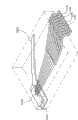
图1A~1E为一系列的俯视图,显示本发明较佳实施例的用于半导体封装的导线架。请参考图1A~1E,本发明的导线架具有一芯片垫10、一边框(siderail)30、联结杆(tie bar)21~24、与多个引脚141~146、241、242、245、341。边框30围绕芯片垫10,联结杆21~24连接芯片垫10与边框30,上述引脚从边框30延伸向芯片垫10,到达邻近芯片垫10之处。在某些情况中,边框30会在后续半导体封装工艺的裁切或分离步骤中移除。1A-1E are a series of top views showing a lead frame for a semiconductor package according to a preferred embodiment of the present invention. 1A-1E, the lead frame of the present invention has a
通过本发明可对一电子元件的阻抗作变化,例如可通过下列手段控制阻抗值:改变引脚长度、改变引脚间的间距(pitch)、改变引脚间的间隙(spacing)、及/或改变引脚的宽度。因此为了个别地调整引脚的阻抗,本发明提供非对称的导线架结构。The impedance of an electronic component can be changed through the present invention, for example, the impedance value can be controlled by the following means: changing the length of the pins, changing the pitch between the pins, changing the spacing between the pins (spacing), and/or Change the width of the pins. Therefore, in order to individually adjust the impedance of the pins, the present invention provides an asymmetric lead frame structure.
在图1A~1E中,每个引脚具有相对于一预定的中心线而位于所述中心线相反侧的对应引脚。在本实施例中,一例示的中心线50绘示于图1A~1E。例如在图1A~1E中,引脚241分别对应于各图所示的引脚141a~141e,而引脚245则对应于引脚145。在本实施例中,本发明的导线架具有一对彼此对应的引脚,其包含一引脚及其对应引脚,但是二者彼此不对称。具体而言,上述不对称的设计用于阻抗匹配。例如相对于中心线50,引脚241的对应引脚分别是引脚141a~141e(分别绘示于图1A~1E),且引脚241分别不对称于其对应引脚141a~141e。图1A~1E分别例示用于非对称的导线架结构的各种非对称的引脚形式。In FIGS. 1A-1E , each pin has a corresponding pin on the opposite side of a predetermined centerline with respect to said centerline. In this embodiment, an exemplary
在某些情况中,一特定引脚的对应引脚会因所选择的中心线(例如本实施例的中心线50)的不同而有所改变。例如在图1A中,相对于中心线50,引脚141a与引脚241对应;而相对于另一穿越引脚143与144之间的间隙的中心线(未绘示),引脚141a则与引脚146对应;另外,相对于穿越联结杆21且与其对准的中心线(未绘示),引脚141a则与引脚341对应。在本实施例后续的讨论中,以中心线50作为例示的中心线。In some cases, the corresponding pin for a particular pin will vary depending on the centerline selected (eg,
请参考图1A~1E,相对于中心线50,引脚141a~141e分别与引脚241在引脚外观或其延伸路径方面,呈现不对称的状态。一对相对于一中心线为对应、但不对称的引脚,是指其具有互异的形状、尺寸、或个别与导线架其它部件的对应关系。Please refer to FIGS. 1A˜1E , relative to the
在图1A中,引脚141a与241具有不同的长度,故为一对不对称的对应引脚。因此,比较对应的引脚141a与241,二者在长度上的不同会使其具有不同的电阻值,故可通过引脚长度的调整来达成所需要的阻抗匹配。In FIG. 1A, the
在图1B中,引脚141b与241具有相同的宽度,然而引脚141b与其相邻引脚例如引脚142的间隙S1,大于引脚241与其相邻引脚例如引脚242的间隙S2。另外,引脚141b与其相邻引脚例如引脚142的间距P1,大于引脚241与其相邻引脚例如引脚242的间距P2。因此,引脚141b与241为一对不对称的对应引脚。故比较对应的引脚141b与241,引脚间隙的变化会使引脚间的电感/电容值发生变化,而可通过引脚间隙的调整来达成所需要的阻抗匹配。In FIG. 1B , pins 141b and 241 have the same width, but the gap S1 between
在图1C中,引脚141c与引脚142c的宽度分别与对应的引脚241与242的宽度不同。另外,引脚141c与其相邻引脚例如引脚142c的间隙S1,小于引脚241与其相邻引脚例如引脚242的间隙S2。因此,引脚141c与241为一对不对称的对应引脚,引脚142c与242也为一对不对称的对应引脚。故比较对应的引脚141c与241、或是对应的引脚142c与242,引脚宽度的变化会使对应的二个引脚具有不同的电阻值,而可通过引脚宽度的调整来达成所需要的阻抗匹配。In FIG. 1C , the
在图1D中,引脚141d与其相邻引脚例如引脚142d的间距P1,大于引脚241与其相邻引脚例如引脚242的间距P2。因此,引脚141d与241为一对不对称的对应引脚。故比较对应的引脚141d与241,引脚间距的变化会使引脚间的电感/电容值发生变化,而可通过引脚间距的调整来达成所需要的阻抗匹配。In FIG. 1D , the distance P1 between the lead 141 d and its adjacent lead, such as the lead 142 d , is greater than the distance P2 between the lead 241 and its adjacent lead, such as the
在图1E中,引脚141e与其相邻引脚例如引脚142的间距P1,小于引脚241与其相邻引脚例如引脚242的间距P2。因此,引脚141e与241为一对不对称的对应引脚。故比较对应的引脚141e与241,引脚间距的变化会使引脚间的电感/电容值发生变化,而可通过引脚间距的调整来达成所需要的阻抗匹配。In FIG. 1E , the distance P1 between the lead 141 e and its adjacent lead, such as the
接下来,一传统的对称导线架绘示于图2A、2B中,作为对照组;而二组本发明的实施例则分别绘示于图3A、3B与图4A、4B中,用以表示本发明的功效。Next, a traditional symmetrical lead frame is shown in FIGS. 2A and 2B as a control group; and two groups of embodiments of the present invention are shown in FIGS. 3A and 3B and FIGS. 4A and 4B respectively to represent the present invention. The efficacy of the invention.
图2A显示一传统的半导体集成电路,其包含一传统的对称导线架、一半导体芯片2100、多条焊线2200、与一封装绝缘体(未绘示),其中半导体芯片2100包含多个导电垫片(electrode pad,未绘示)黏着于上述导线架的芯片垫2010上,焊线2200电性连接所述导电垫片与上述导线架的引脚,半导体芯片2100、上述导线架、与焊线2200则封入上述封装绝缘体中。上述导线架包含一芯片垫2010、四个联结杆2021~2024、与多个引脚,其中联结杆2021~2024用以支撑芯片垫2010。上述导线架的边框则已在半导体封装工艺的裁切或分离步骤中移除。上述导线架的引脚的延伸路径与外观等各方面呈现实质上对称的状态。2A shows a conventional semiconductor integrated circuit, which includes a conventional symmetrical lead frame, a
图2B显示图2A中例示的引脚1145、1146、1148、与1149的放大图。例如传输频率约750MHz的电子信号的情况下,在引脚1145、1146间所构成的差动阻抗(differential impedance)值约为68欧姆;相同地,在引脚1148、1149间所构成的差动阻抗值约为68欧姆;另外引脚1145、1146、1148、与1149的单端阻抗(single-ended impedance)约为50欧姆。然而在某些情况中,某些引脚对的差动阻抗需要80~120欧姆、较佳为100欧姆;或是某些引脚的单端阻抗需要40~60欧姆、较佳为50欧姆。因此,使用上述传统的导线架无法符合所需要的阻抗值。FIG. 2B shows an enlarged view of
图3A显示本发明另一实施例的半导体集成电路的俯视图,将其与绘示于图2A的半导体集成电路比较,引脚1145、1146、1148、与1149的长度减少了D。在本实施例中,D值约为60mil.。FIG. 3A shows a top view of a semiconductor integrated circuit according to another embodiment of the present invention. Compared with the semiconductor integrated circuit shown in FIG. 2A , the lengths of the
图3B显示图3A中已缩短的引脚1145、1146、1148、与1149的放大图。例如传输频率约750MHz的电子信号的情况下,在引脚1145、1146间所构成的差动阻抗(differential impedance)值约为84欧姆,而符合上述阻抗值的需求;相同地,在引脚1148、1149所构成的差动阻抗值约为84欧姆,也符合上述阻抗值的需求;另外引脚1145、1146、1148、与1149的单端阻抗约为58欧姆。此一实施例的半导体集成电路受惠于其使用本发明的导线架结构,其可达成某些既定的引脚对于阻抗值的需求,而满足阻抗匹配所需的阻抗值。FIG. 3B shows an enlarged view of shortened
图4A显示本发明另一实施例的半导体集成电路的俯视图,将其与绘示于图2A的半导体集成电路比较,将引脚1145与1146之间的间隙、以及引脚1148与1149之间的间隙加宽。FIG. 4A shows a top view of a semiconductor integrated circuit according to another embodiment of the present invention. Comparing it with the semiconductor integrated circuit shown in FIG. The gap widens.
图4B显示图4A中的引脚1145、1146、1148、与1149的放大图。例如传输频率约750MHz的电子信号的情况下,在引脚1145、1146间所构成的差动阻抗(differential impedance)值约为108欧姆,而符合上述阻抗值的需求;相同地,在引脚1148、1149间所构成的差动阻抗值约为108欧姆,亦符合上述阻抗值的需求;另外引脚1145、1146、1148、与1149的单端阻抗约为62欧姆。本实施例的半导体集成电路受惠于其使用本发明的导线架结构,其可达成某些既定的引脚对于阻抗值的需求,满足阻抗匹配所需的阻抗值。FIG. 4B shows an enlarged view of
综上所述,本发明通过发展出非对称的引脚延伸路径或引脚分布,而能对所制造的产品提供有效的阻抗匹配。To sum up, the present invention can provide effective impedance matching to manufactured products by developing an asymmetrical pin extension path or pin distribution.
虽然本发明已以较佳实施例揭露如上,然其并非用以限定本发明,任何本发明所属技术领域中具有通常知识者,在不脱离本发明的精神和范围内,当可作些许的更动与润饰,因此本发明的保护范围当视后附的申请专利范围所界定者为准。Although the present invention has been disclosed above with preferred embodiments, it is not intended to limit the present invention. Anyone with ordinary knowledge in the technical field of the present invention can make some modifications without departing from the spirit and scope of the present invention. Therefore, the scope of protection of the present invention should be defined by the scope of the appended patent application.
Claims (18)
Applications Claiming Priority (2)
| Application Number | Priority Date | Filing Date | Title |
|---|---|---|---|
| US73177905P | 2005-10-31 | 2005-10-31 | |
| US60/731,779 | 2005-10-31 |
Related Child Applications (1)
| Application Number | Title | Priority Date | Filing Date |
|---|---|---|---|
| CN200910137099.9ADivisionCN101546744B (en) | 2005-10-31 | 2006-10-31 | Lead frame for semiconductor packaging |
Publications (2)
| Publication Number | Publication Date |
|---|---|
| CN1959975A CN1959975A (en) | 2007-05-09 |
| CN100505231Ctrue CN100505231C (en) | 2009-06-24 |
Family
ID=38071564
Family Applications (2)
| Application Number | Title | Priority Date | Filing Date |
|---|---|---|---|
| CNB2006101427866AActiveCN100505231C (en) | 2005-10-31 | 2006-10-31 | Semiconductor integrated circuit and packaging lead frame thereof |
| CN200910137099.9AActiveCN101546744B (en) | 2005-10-31 | 2006-10-31 | Lead frame for semiconductor packaging |
Family Applications After (1)
| Application Number | Title | Priority Date | Filing Date |
|---|---|---|---|
| CN200910137099.9AActiveCN101546744B (en) | 2005-10-31 | 2006-10-31 | Lead frame for semiconductor packaging |
Country Status (3)
| Country | Link |
|---|---|
| US (3) | US20070096269A1 (en) |
| CN (2) | CN100505231C (en) |
| TW (1) | TWI354357B (en) |
Families Citing this family (7)
| Publication number | Priority date | Publication date | Assignee | Title |
|---|---|---|---|---|
| JP4595835B2 (en)* | 2006-03-07 | 2010-12-08 | 株式会社日立製作所 | Leaded electronic parts using lead-free solder |
| US7468547B2 (en)* | 2007-05-11 | 2008-12-23 | Intersil Americas Inc. | RF-coupled digital isolator |
| CN101572257B (en)* | 2008-04-30 | 2011-02-16 | 南茂科技股份有限公司 | Chip packaging tape and chip packaging structure including the chip packaging tape |
| US20100171201A1 (en)* | 2009-01-06 | 2010-07-08 | Wyant M Todd | Chip on lead with small power pad design |
| US9837188B2 (en)* | 2012-07-06 | 2017-12-05 | Nxp B.V. | Differential return loss supporting high speed bus interfaces |
| US20170245361A1 (en)* | 2016-01-06 | 2017-08-24 | Nokomis, Inc. | Electronic device and methods to customize electronic device electromagnetic emissions |
| TWI623076B (en)* | 2016-11-02 | 2018-05-01 | 復盛精密工業股份有限公司 | Method for manufacturing leadframe |
Citations (5)
| Publication number | Priority date | Publication date | Assignee | Title |
|---|---|---|---|---|
| US5517056A (en)* | 1993-09-30 | 1996-05-14 | Motorola, Inc. | Molded carrier ring leadframe having a particular resin injecting area design for gate removal and semiconductor device employing the same |
| US5541565A (en)* | 1995-05-22 | 1996-07-30 | Trw Inc. | High frequency microelectronic circuit enclosure |
| US5608265A (en)* | 1993-03-17 | 1997-03-04 | Hitachi, Ltd. | Encapsulated semiconductor device package having holes for electrically conductive material |
| US5757067A (en)* | 1995-12-20 | 1998-05-26 | Nec Corporation | Resin-sealed type semiconductor device |
| US6281568B1 (en)* | 1998-10-21 | 2001-08-28 | Amkor Technology, Inc. | Plastic integrated circuit device package and leadframe having partially undercut leads and die pad |
Family Cites Families (17)
| Publication number | Priority date | Publication date | Assignee | Title |
|---|---|---|---|---|
| US3793474A (en)* | 1971-12-09 | 1974-02-19 | Motorola Inc | Lead configurations for plastic encapsulated semiconductor devices |
| US4454529A (en)* | 1981-01-12 | 1984-06-12 | Avx Corporation | Integrated circuit device having internal dampening for a plurality of power supplies |
| US4680613A (en)* | 1983-12-01 | 1987-07-14 | Fairchild Semiconductor Corporation | Low impedance package for integrated circuit die |
| JPS61269345A (en)* | 1985-05-24 | 1986-11-28 | Hitachi Ltd | Semiconductor device |
| US5065224A (en)* | 1986-06-30 | 1991-11-12 | Fairchild Semiconductor Corporation | Low noise integrated circuit and leadframe |
| US5147815A (en)* | 1990-05-14 | 1992-09-15 | Motorola, Inc. | Method for fabricating a multichip semiconductor device having two interdigitated leadframes |
| US5281849A (en)* | 1991-05-07 | 1994-01-25 | Singh Deo Narendra N | Semiconductor package with segmented lead frame |
| JPH0714976A (en)* | 1993-06-24 | 1995-01-17 | Shinko Electric Ind Co Ltd | Lead frame and semiconductor device |
| KR0149798B1 (en)* | 1994-04-15 | 1998-10-01 | 모리시다 요이치 | Semiconductor device and method of manufacture and lead frame |
| KR100372153B1 (en)* | 1995-04-05 | 2003-06-19 | 내셔널 세미콘덕터 코포레이션 | Multi-layer lead frame |
| US5918112A (en)* | 1997-07-24 | 1999-06-29 | Motorola, Inc. | Semiconductor component and method of fabrication |
| US6509632B1 (en)* | 1998-01-30 | 2003-01-21 | Micron Technology, Inc. | Method of fabricating a redundant pinout configuration for signal enhancement in an IC package |
| US6424541B1 (en)* | 1999-04-21 | 2002-07-23 | Conexant Systems, Inc | Electronic device attachment methods and apparatus for forming an assembly |
| KR100379089B1 (en)* | 1999-10-15 | 2003-04-08 | 앰코 테크놀로지 코리아 주식회사 | leadframe and semiconductor package using it |
| US6621140B1 (en)* | 2002-02-25 | 2003-09-16 | Rf Micro Devices, Inc. | Leadframe inductors |
| US7005325B2 (en)* | 2004-02-05 | 2006-02-28 | St Assembly Test Services Ltd. | Semiconductor package with passive device integration |
| TWI252572B (en)* | 2004-06-30 | 2006-04-01 | Orient Semiconductor Elect Ltd | Package structure |
- 2006
- 2006-10-06USUS11/539,239patent/US20070096269A1/ennot_activeAbandoned
- 2006-10-23TWTW095139004Apatent/TWI354357B/enactive
- 2006-10-31CNCNB2006101427866Apatent/CN100505231C/enactiveActive
- 2006-10-31CNCN200910137099.9Apatent/CN101546744B/enactiveActive
- 2010
- 2010-04-12USUS12/758,141patent/US20100193925A1/ennot_activeAbandoned
- 2013
- 2013-12-09USUS14/100,444patent/US9198281B2/enactiveActive
Patent Citations (5)
| Publication number | Priority date | Publication date | Assignee | Title |
|---|---|---|---|---|
| US5608265A (en)* | 1993-03-17 | 1997-03-04 | Hitachi, Ltd. | Encapsulated semiconductor device package having holes for electrically conductive material |
| US5517056A (en)* | 1993-09-30 | 1996-05-14 | Motorola, Inc. | Molded carrier ring leadframe having a particular resin injecting area design for gate removal and semiconductor device employing the same |
| US5541565A (en)* | 1995-05-22 | 1996-07-30 | Trw Inc. | High frequency microelectronic circuit enclosure |
| US5757067A (en)* | 1995-12-20 | 1998-05-26 | Nec Corporation | Resin-sealed type semiconductor device |
| US6281568B1 (en)* | 1998-10-21 | 2001-08-28 | Amkor Technology, Inc. | Plastic integrated circuit device package and leadframe having partially undercut leads and die pad |
Also Published As
| Publication number | Publication date |
|---|---|
| TW200717762A (en) | 2007-05-01 |
| US9198281B2 (en) | 2015-11-24 |
| US20100193925A1 (en) | 2010-08-05 |
| CN101546744A (en) | 2009-09-30 |
| US20070096269A1 (en) | 2007-05-03 |
| TWI354357B (en) | 2011-12-11 |
| CN101546744B (en) | 2014-05-21 |
| US20140097012A1 (en) | 2014-04-10 |
| CN1959975A (en) | 2007-05-09 |
Similar Documents
| Publication | Publication Date | Title |
|---|---|---|
| CN100505231C (en) | Semiconductor integrated circuit and packaging lead frame thereof | |
| US5304743A (en) | Multilayer IC semiconductor package | |
| US7378743B2 (en) | Circuit board and electronic assembly | |
| CN101471317A (en) | Lead frame package and lead frame | |
| CN110534498B (en) | Packaged semiconductor devices | |
| JP2004095572A (en) | Semiconductor device and method of manufacturing the same | |
| US7531751B2 (en) | Method and system for an improved package substrate for use with a semiconductor package | |
| US7247937B2 (en) | Mounting pad structure for wire-bonding type lead frame packages | |
| CN101604677A (en) | Improving Techniques for Return Loss in Wire Bond Packages for High Speed Data Communications | |
| JP2009088063A (en) | Semiconductor apparatus and method of designing the same | |
| TWI740569B (en) | Wiring board and semiconductor device | |
| US7122892B2 (en) | Multi-chip integrated circuit module for high-frequency operation | |
| US7804167B2 (en) | Wire bond integrated circuit package for high speed I/O | |
| TWI430413B (en) | Semiconductor device | |
| KR102830332B1 (en) | Semiconductor package | |
| TWI761052B (en) | Integrated circuit lead frame and semiconductor device thereof | |
| CN104795379A (en) | Differential coplanar transmission line encapsulation pin inside and outside cascade structure | |
| US8957507B2 (en) | Technology of reducing radiation noise of semiconductor device | |
| CN114864531A (en) | Integrated circuit lead frame and semiconductor device thereof | |
| JP2904186B2 (en) | Semiconductor device | |
| US20060103002A1 (en) | Semiconductor packages with asymmetric connection configurations | |
| CN118919512A (en) | Semiconductor package including auxiliary conductors coupled to trace patterns | |
| CN2521757Y (en) | Flip Chip Pad Configuration on Die for Reduced Impedance | |
| JP2013222954A (en) | Semiconductor device | |
| JP2010074034A (en) | Lead frame, and resin sealed semiconductor device |
Legal Events
| Date | Code | Title | Description |
|---|---|---|---|
| C06 | Publication | ||
| PB01 | Publication | ||
| C10 | Entry into substantive examination | ||
| SE01 | Entry into force of request for substantive examination | ||
| C14 | Grant of patent or utility model | ||
| GR01 | Patent grant |