CN100505152C - Method of forming micropatterns in semiconductor devices - Google Patents
Method of forming micropatterns in semiconductor devicesDownload PDFInfo
- Publication number
- CN100505152C CN100505152CCNB2006100673577ACN200610067357ACN100505152CCN 100505152 CCN100505152 CCN 100505152CCN B2006100673577 ACNB2006100673577 ACN B2006100673577ACN 200610067357 ACN200610067357 ACN 200610067357ACN 100505152 CCN100505152 CCN 100505152C
- Authority
- CN
- China
- Prior art keywords
- film
- polysilicon
- polishing
- photoresist
- oxide film
- Prior art date
- Legal status (The legal status is an assumption and is not a legal conclusion. Google has not performed a legal analysis and makes no representation as to the accuracy of the status listed.)
- Expired - Fee Related
Links
Images


Classifications
- H—ELECTRICITY
- H01—ELECTRIC ELEMENTS
- H01L—SEMICONDUCTOR DEVICES NOT COVERED BY CLASS H10
- H01L21/00—Processes or apparatus adapted for the manufacture or treatment of semiconductor or solid state devices or of parts thereof
- H01L21/02—Manufacture or treatment of semiconductor devices or of parts thereof
- H01L21/027—Making masks on semiconductor bodies for further photolithographic processing not provided for in group H01L21/18 or H01L21/34
- H01L21/033—Making masks on semiconductor bodies for further photolithographic processing not provided for in group H01L21/18 or H01L21/34 comprising inorganic layers
- H01L21/0334—Making masks on semiconductor bodies for further photolithographic processing not provided for in group H01L21/18 or H01L21/34 comprising inorganic layers characterised by their size, orientation, disposition, behaviour, shape, in horizontal or vertical plane
- H01L21/0337—Making masks on semiconductor bodies for further photolithographic processing not provided for in group H01L21/18 or H01L21/34 comprising inorganic layers characterised by their size, orientation, disposition, behaviour, shape, in horizontal or vertical plane characterised by the process involved to create the mask, e.g. lift-off masks, sidewalls, or to modify the mask, e.g. pre-treatment, post-treatment
- H—ELECTRICITY
- H01—ELECTRIC ELEMENTS
- H01L—SEMICONDUCTOR DEVICES NOT COVERED BY CLASS H10
- H01L21/00—Processes or apparatus adapted for the manufacture or treatment of semiconductor or solid state devices or of parts thereof
- H01L21/02—Manufacture or treatment of semiconductor devices or of parts thereof
- H01L21/027—Making masks on semiconductor bodies for further photolithographic processing not provided for in group H01L21/18 or H01L21/34
- H01L21/033—Making masks on semiconductor bodies for further photolithographic processing not provided for in group H01L21/18 or H01L21/34 comprising inorganic layers
- H01L21/0334—Making masks on semiconductor bodies for further photolithographic processing not provided for in group H01L21/18 or H01L21/34 comprising inorganic layers characterised by their size, orientation, disposition, behaviour, shape, in horizontal or vertical plane
- H01L21/0338—Process specially adapted to improve the resolution of the mask
- H—ELECTRICITY
- H01—ELECTRIC ELEMENTS
- H01L—SEMICONDUCTOR DEVICES NOT COVERED BY CLASS H10
- H01L21/00—Processes or apparatus adapted for the manufacture or treatment of semiconductor or solid state devices or of parts thereof
- H01L21/02—Manufacture or treatment of semiconductor devices or of parts thereof
- H01L21/04—Manufacture or treatment of semiconductor devices or of parts thereof the devices having potential barriers, e.g. a PN junction, depletion layer or carrier concentration layer
- H01L21/18—Manufacture or treatment of semiconductor devices or of parts thereof the devices having potential barriers, e.g. a PN junction, depletion layer or carrier concentration layer the devices having semiconductor bodies comprising elements of Group IV of the Periodic Table or AIIIBV compounds with or without impurities, e.g. doping materials
- H01L21/30—Treatment of semiconductor bodies using processes or apparatus not provided for in groups H01L21/20 - H01L21/26
- H01L21/31—Treatment of semiconductor bodies using processes or apparatus not provided for in groups H01L21/20 - H01L21/26 to form insulating layers thereon, e.g. for masking or by using photolithographic techniques; After treatment of these layers; Selection of materials for these layers
- H01L21/3105—After-treatment
- H01L21/31051—Planarisation of the insulating layers
- H—ELECTRICITY
- H01—ELECTRIC ELEMENTS
- H01L—SEMICONDUCTOR DEVICES NOT COVERED BY CLASS H10
- H01L21/00—Processes or apparatus adapted for the manufacture or treatment of semiconductor or solid state devices or of parts thereof
- H01L21/02—Manufacture or treatment of semiconductor devices or of parts thereof
- H01L21/04—Manufacture or treatment of semiconductor devices or of parts thereof the devices having potential barriers, e.g. a PN junction, depletion layer or carrier concentration layer
- H01L21/18—Manufacture or treatment of semiconductor devices or of parts thereof the devices having potential barriers, e.g. a PN junction, depletion layer or carrier concentration layer the devices having semiconductor bodies comprising elements of Group IV of the Periodic Table or AIIIBV compounds with or without impurities, e.g. doping materials
- H01L21/30—Treatment of semiconductor bodies using processes or apparatus not provided for in groups H01L21/20 - H01L21/26
- H01L21/31—Treatment of semiconductor bodies using processes or apparatus not provided for in groups H01L21/20 - H01L21/26 to form insulating layers thereon, e.g. for masking or by using photolithographic techniques; After treatment of these layers; Selection of materials for these layers
- H01L21/3205—Deposition of non-insulating-, e.g. conductive- or resistive-, layers on insulating layers; After-treatment of these layers
- H01L21/321—After treatment
- H01L21/3213—Physical or chemical etching of the layers, e.g. to produce a patterned layer from a pre-deposited extensive layer
- H01L21/32139—Physical or chemical etching of the layers, e.g. to produce a patterned layer from a pre-deposited extensive layer using masks
- H—ELECTRICITY
- H10—SEMICONDUCTOR DEVICES; ELECTRIC SOLID-STATE DEVICES NOT OTHERWISE PROVIDED FOR
- H10B—ELECTRONIC MEMORY DEVICES
- H10B41/00—Electrically erasable-and-programmable ROM [EEPROM] devices comprising floating gates
- H10B41/40—Electrically erasable-and-programmable ROM [EEPROM] devices comprising floating gates characterised by the peripheral circuit region
- H10B41/42—Simultaneous manufacture of periphery and memory cells
- H10B41/49—Simultaneous manufacture of periphery and memory cells comprising different types of peripheral transistor
Landscapes
- Engineering & Computer Science (AREA)
- Manufacturing & Machinery (AREA)
- Microelectronics & Electronic Packaging (AREA)
- Power Engineering (AREA)
- Condensed Matter Physics & Semiconductors (AREA)
- General Physics & Mathematics (AREA)
- Physics & Mathematics (AREA)
- Computer Hardware Design (AREA)
- Inorganic Chemistry (AREA)
- Chemical & Material Sciences (AREA)
- Internal Circuitry In Semiconductor Integrated Circuit Devices (AREA)
- Semiconductor Memories (AREA)
- Exposure Of Semiconductors, Excluding Electron Or Ion Beam Exposure (AREA)
- Photosensitive Polymer And Photoresist Processing (AREA)
- Exposure And Positioning Against Photoresist Photosensitive Materials (AREA)
- Electrodes Of Semiconductors (AREA)
- Mechanical Treatment Of Semiconductor (AREA)
Abstract
Description
Translated fromChinese技术领域technical field
本发明总体涉及一种制造半导体器件的方法,更具体地,涉及一种在半导体器件内形成微图案的方法,其中微图案的节距低于曝光设备的分辨能力。The present invention generally relates to a method of manufacturing a semiconductor device, and more particularly, to a method of forming micropatterns in a semiconductor device, wherein the pitch of the micropatterns is lower than the resolution capability of exposure equipment.
背景技术Background technique
制造半导体器件时,在光刻工艺中形成的图案的最小节距是由所使用的曝光辐射的波形所决定的。因此,随着半导体器件越来越集成化,为了形成具有更小节距的图案,必须使用具有比现行辐射波形更短的辐射。为达到此目的,可优选使用X射线或电子束。然而,由于技术问题,生产率等原因,X射线或电子束的使用尚未实现商业化。基于上述原因,现提出双曝光和蚀刻技术(DEET)。When manufacturing semiconductor devices, the minimum pitch of patterns formed in the photolithography process is determined by the waveform of the exposure radiation used. Therefore, as semiconductor devices become more and more integrated, in order to form patterns with smaller pitches, it is necessary to use radiation having a shorter waveform than the current radiation. For this purpose, X-rays or electron beams may preferably be used. However, the use of X-rays or electron beams has not been commercialized due to technical issues, productivity, etc. Based on the above reasons, a double exposure and etching technique (DEET) is now proposed.
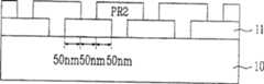
图1A至1C是显示双曝光蚀刻技术的示意图。如图1A所示,第一光致抗蚀剂PR1涂布在具有待蚀刻层11的半导体衬底10上。在通过曝光和显影工艺构图第一光致抗蚀剂PR1后,使用构图的第一光致抗蚀剂PR1作为掩模,对待蚀刻层11进行蚀刻。蚀刻后的待蚀刻层11具有150nm的线宽和50nm的间隔宽度。1A to 1C are schematic diagrams showing a double exposure etching technique. As shown in FIG. 1A, a first photoresist PR1 is coated on a
之后,剥去第一光致抗蚀剂PR1,且将第二光致抗蚀剂PR2涂布在整个结构上。通过曝光和显影工艺构图第二光致抗蚀剂PR2,以便能够如图1B所示暴露待蚀刻层11的一部分。After that, the first photoresist PR1 is stripped, and the second photoresist PR2 is coated on the entire structure. The second photoresist PR2 is patterned through exposure and development processes so that a portion of the layer to be etched 11 can be exposed as shown in FIG. 1B .
如图1C所示,使用构图的第二光致抗蚀剂PR2作为掩模,对待蚀刻层11再一次进行蚀刻,并由此形成具有线宽和间隔宽度为50nm的最终图案。然后剥去第二光致抗蚀剂PR2。As shown in FIG. 1C , using the patterned second photoresist PR2 as a mask, the
在上述双曝光蚀刻技术中,在第二光致抗蚀剂PR2的曝光工艺中,覆盖准确度与最后图案的临界尺寸(CD)偏差直接关联。在实际中,由于很难将曝光设备的覆盖准确度控制在10nm或更小的范围内,所以很难降低最终图案的CD偏差。依靠曝光,也很难由电路的分离控制光学临近修正度(OPC)。In the above double exposure etching technique, in the exposure process of the second photoresist PR2, the coverage accuracy is directly related to the critical dimension (CD) deviation of the final pattern. In practice, it is difficult to reduce the CD deviation of the final pattern because it is difficult to control the coverage accuracy of the exposure equipment in the range of 10nm or less. Depending on the exposure, it is also difficult to control the optical proximity correction (OPC) by the separation of the circuit.
发明内容Contents of the invention
本发明提供了在半导体器件内形成可以降低图案CD偏差的微图案的方法。The present invention provides a method of forming a micropattern capable of reducing pattern CD deviation in a semiconductor device.
根据本发明的一方面,一种形成半导体器件内微图案的方法包括以下步骤:(a)在具有待蚀刻层的半导体衬底上依次形成第一多晶硅膜和覆盖在第一多晶硅膜之上的缓冲氧化物膜,然后形成具有一种结构的硬掩模,在该结构中,在该缓冲氧化物膜的预定区域内层积第二多晶硅膜、抗抛光膜和第一氧化物膜,(b)在硬掩模的侧部上形成氮化物膜间隔物,并在整个结构上形成第二氧化物膜,(c)抛光第二氧化物膜、该氮化物膜间隔物和第一氧化物膜,以便暴露抗抛光膜,并移除抗抛光膜和氮化物膜间隔物,(d)用第二多晶硅膜和第二氧化物膜作为掩模,蚀刻该缓冲氧化物膜,并移除第二氧化物膜,(e)用第二多晶硅膜和缓冲氧化物膜作为掩模,蚀刻第一多晶硅膜,并移除第二多晶硅膜,以及(f)用缓冲氧化物膜和第一多晶硅膜作为掩模,蚀刻待蚀刻层。According to one aspect of the present invention, a kind of method for forming micropattern in semiconductor device comprises the following steps: (a) on the semiconductor substrate that has to-be-etched layer, form first polysilicon film and cover on the first polysilicon film successively buffer oxide film over the buffer oxide film, and then form a hard mask having a structure in which a second polysilicon film, an anti-polishing film, and a first oxide film, (b) forming a nitride film spacer on the side portion of the hard mask, and forming a second oxide film on the entire structure, (c) polishing the second oxide film, the nitride film spacer and the first oxide film, so that the anti-polishing film is exposed, and the anti-polishing film and the nitride film spacer are removed, (d) using the second polysilicon film and the second oxide film as a mask, the buffered oxide film is etched and removing the second oxide film, (e) using the second polysilicon film and the buffer oxide film as a mask, etching the first polysilicon film, and removing the second polysilicon film, and (f) Using the buffer oxide film and the first polysilicon film as masks, the layer to be etched is etched.
在步骤(d)和步骤(e)之间,该方法还可以包括移除形成在不应形成图案的部分中的缓冲氧化物膜的预定部分的步骤(g)。Between the step (d) and the step (e), the method may further include a step (g) of removing a predetermined portion of the buffer oxide film formed in a portion that should not be patterned.
步骤(g)可以包括以下步骤:(g1)在整个结构上依次形成第二抗反射膜和覆盖于第二抗反射膜之上的第二光致抗蚀剂,(g2)构图第二光致抗蚀剂,以便将在不应形成图案的部分中形成的缓冲氧化物膜上的第二抗反射膜暴露出来,(g3)使用构图的第二光致抗蚀剂作为掩模,蚀刻第二抗反射膜和缓冲氧化物膜,以及(g4)移除第二光致抗蚀剂和第二抗反射膜。Step (g) may include the following steps: (g1) sequentially forming a second antireflection film and a second photoresist covering the second antireflection film on the entire structure, (g2) patterning the second photoresist resist, so that the second antireflection film on the buffer oxide film formed in the portion that should not be patterned is exposed, (g3) using the patterned second photoresist as a mask, etching the second anti-reflection film and buffer oxide film, and (g4) removing the second photoresist and the second anti-reflection film.
该方法可以进一步包括在第一多晶硅膜形成之前,形成用于保护下面的待蚀刻层的保护层的步骤。该保护层可以使用SiON膜,形成到
该方法还可以包括在保护层形成之前,形成第一α-碳膜的步骤。第一α-碳膜可以形成

第一多晶硅膜一般形成


硬掩模可以利用以下的步骤形成:在缓冲氧化物膜整个表面上依次形成第二多晶硅膜,第二多晶硅之上的抗抛光膜和抗抛光膜之上的第一氧化物膜;形成第一氧化物膜上的第二α-碳膜;在第二α-碳膜上涂布第一光致抗蚀剂,并构图第一光致抗蚀剂,使用构图的第一光致抗蚀剂作为掩模,蚀刻第二α-碳膜、第一氧化物膜、抗抛光膜和第二多晶硅膜,并且移除蚀刻工艺后残留的第一光致抗蚀剂和第二α-碳膜。The hard mask can be formed using the steps of sequentially forming a second polysilicon film on the entire surface of the buffer oxide film, an anti-polishing film over the second polysilicon, and a first oxide film over the anti-polishing film. ; forming a second α-carbon film on the first oxide film; coating a first photoresist on the second α-carbon film, and patterning the first photoresist, using patterned first light Using the photoresist as a mask, the second α-carbon film, the first oxide film, the anti-polishing film, and the second polysilicon film are etched, and the first photoresist and the second photoresist remaining after the etching process are removed. Two alpha-carbon films.
该方法还可以包括在涂布第一光致抗蚀剂之前,依次形成第二保护层和该第二保护层之上的抗反射膜。The method may further include sequentially forming a second protection layer and an anti-reflection film on the second protection layer before coating the first photoresist.
使用SiON膜的第二保护层一般形成


在步骤(c)中,可以先由过抛光工艺移除抗抛光膜,再移除氮化物膜间隔物。In step (c), the anti-polishing film may be removed by an over-polishing process first, and then the nitride film spacer may be removed.
在步骤(c)中,抗抛光膜和氮化物膜间隔物可以同时移除。In step (c), the anti-polishing film and the nitride film spacer may be removed simultaneously.
附图说明Description of drawings
图1A至1C是示出现有技术双曝光蚀刻技术的示意图;并且1A to 1C are schematic diagrams illustrating prior art double exposure etching techniques; and
图2A至2K是示出根据本发明的一个实施例,在半导体器件内形成微图案工艺的截面示意图。2A to 2K are schematic cross-sectional views illustrating a process for forming micropatterns in a semiconductor device according to an embodiment of the present invention.
具体实施方式Detailed ways
下面将参照附图,结合优选实施例对本发明进行描述。The present invention will be described below in conjunction with preferred embodiments with reference to the accompanying drawings.
由于提供优选实施例的目的是使该技术中普通技术人员理解本发明,它们可以进行多种方式的修改,而且本发明的范围也不仅限于下面描述的优选实施例。Since the preferred embodiments are provided for the purpose of making the present invention understandable to those skilled in the art, they can be modified in various ways, and the scope of the present invention is not limited only to the preferred embodiments described below.
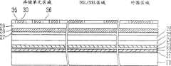
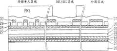
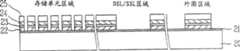
图2A至2K是示出根据本发明一个实施例,在半导体器件内形成微图案工艺的截面示意图。图2显示了本发明应用于闪存存储器的栅极蚀刻工艺的一个示例。2A to 2K are schematic cross-sectional views illustrating a process of forming micropatterns in a semiconductor device according to an embodiment of the present invention. FIG. 2 shows an example of the present invention applied to a gate etching process of a flash memory.
首先根据图2A,隧道氧化物21(即待蚀刻层)、浮置栅导电膜22、介电膜23、控制栅导电膜24和硬掩模氮化物膜25依次形成于将形成存储单元晶体管的半导体衬底20硬存储单元区域、将形成漏极选择线(DSL)/源极选择线(SSL)的DSL/SSL区域,以及将形成外围电路的外围区域之上。硬掩模氮化物膜25是用于自对准接触工艺,且一般形成为

然后,第一多晶硅膜28和缓冲氧化物膜29依次形成于整个结构之上。第一多晶硅膜28一般形成为


在此情况下,在第一多晶硅膜28形成之前,可以进一步形成第一α碳膜26和第一保护膜27。第一α碳膜26用于在随后硬掩模氮化物膜25被蚀刻时,补充蚀刻裕量的短缺,并且它一般形成为到

之后,第二多晶硅膜30、抗抛光膜31和第一氧化物膜32依次形成于缓冲氧化物膜29上。第二多晶硅膜30一般形成为


第二α碳膜33和第二保护层34然后依次形成于第一氧化物膜32上。在第二保护层34上涂布第一光致抗蚀剂PR1。第二α碳膜33是额外形成的膜,用于当蚀刻第一氧化物膜32、抗抛光膜31和第二多晶硅膜30时,补充第一光致抗蚀剂PR1的蚀刻裕量的短缺。第二保护层34一般用SiON膜形成为


同时,虽然未显示于示意图中,但是在涂布第一光致抗蚀剂PR1前,优选一般在第二保护层34上形成具有

然后,一般由曝光和显影工艺构图第一光致抗蚀剂PR1。此时,一般要控制此构图工艺,以便形成于存储单元区域内的第一光致抗蚀剂PR1的线CD变为65nm至75nm,且CD的间隔为115nm至125nm。Then, the first photoresist PR1 is typically patterned by exposure and development processes. At this time, the patterning process is generally controlled so that the line CD of the first photoresist PR1 formed in the memory cell area becomes 65nm to 75nm, and the interval of CD is 115nm to 125nm.
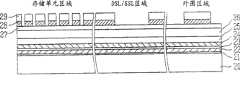
之后,如图2B所示,用已构图的第一光致抗蚀剂PR1作为掩模,蚀刻第二保护层34、第二α碳膜33、第一氧化物膜32、抗抛光膜31和第二多晶硅膜30。此时,一般将线CD偏置控制在5nm至15nm,使得蚀刻的第二多晶硅膜30、蚀刻的抗抛光膜31和蚀刻的第一氧化物膜32的CD一般都在5nm至15nm,比第一光致抗蚀剂PR1的CD小。After that, as shown in FIG. 2B, using the patterned first photoresist PR1 as a mask, the second protective layer 34, the second α-carbon film 33, the
若该工艺按上面的描述进行,可以形成比曝光设备的分辨能力尺寸更小的图案,尽管构图的第一光致抗蚀剂PR1的大小在曝光设备分辨能力的尺寸之内。If the process is performed as described above, a pattern smaller than the resolution of the exposure equipment can be formed, although the size of the patterned first photoresist PR1 is within the resolution of the exposure equipment.
如果第二α碳膜33的厚度小,就很难在蚀刻工艺中确保线CD的偏置。因此,第二α碳膜33必须具有预定的厚度,比如,

然后移除留在第一氧化物膜32上的膜,包括第二α碳膜33。如图2C所示,一般具有

之后,如图2D所示,在整个表面上使用抗抛光膜31作为CMP的停止层进行化学机械抛光(CMP),从而平整地移除第二氧化物膜36和第一氧化物膜32。为移除抗抛光膜31,然后进行一个过(即额外的)CMP工艺。由此,保留了由氮化物膜间隔物35相互分离的第二氧化物膜36和第二多晶硅膜30。此时,虽然在没有移除的抗抛光膜31的情况下进行了后继的工艺,但是可以在随后移除氮化物膜间隔物35时,移除抗抛光膜31。因此,可以省略上面提到的过CMP工艺。After that, as shown in FIG. 2D , chemical mechanical polishing (CMP) is performed on the entire surface using the
同时,在CMP工艺中移除氮化物膜间隔物上的弧形肩部分。因此,CMP工艺后留下的氮化物膜间隔物35,第二氧化物膜36和第二多晶硅膜30很少有高度上的CD偏差。At the same time, the arc-shaped shoulder portion on the nitride film spacer is removed in the CMP process. Therefore, the
如图2E所示,用湿蚀刻工艺移除氮化物膜间隔物35。然后,为了分别控制第二氧化物膜36和第二多晶硅膜30的厚度,进行湿蚀刻工艺。As shown in FIG. 2E, the
之后,如图2F所示,使用第二氧化物膜36和第二多晶硅膜30作为蚀刻阻挡,蚀刻下面的缓冲氧化物膜29。此时,和缓冲氧化物膜29具有相同蚀刻选择比的第二氧化物膜36也被移除,但与缓冲氧化物膜29具有不同蚀刻选择比的第二多晶硅膜30保留在缓冲氧化物膜29上。After that, as shown in FIG. 2F , using the
之后,必须移除在不应形成图案的区域形成的缓冲氧化物膜29。After that, the
如图2G所示,为达到此目的,在整个结构上依次形成第二抗反射膜37和第二光致抗蚀剂PR2。构图第二光致抗蚀剂PR2从而使在不应形成图案的区域内形成的缓冲氧化物膜29上的第二抗反射膜37得以暴露。如图2H所示,在使用已构图的第二光致抗蚀剂PR2作为掩模,蚀刻第二抗反射膜37和缓冲氧化物膜29之后,移除第二光致抗蚀剂PR2和第二抗反射膜37。As shown in FIG. 2G, for this purpose, a
此时,当蚀刻缓冲氧化物膜29时,用第一多晶硅膜28阻止此蚀刻工艺。由此,可以防止下层受到侵蚀。而且,第二多晶硅膜30和缓冲氧化物膜29具有不同的蚀刻选择比。据此,虽然第二光致抗蚀剂PR2不仅敞开了缓冲氧化物膜29,还敞开了与缓冲氧化物膜29相邻的第二多晶硅膜30的上部,但是还是可以在不明显损失第二多晶硅膜30的情况下,移除缓冲氧化物膜29。由此,充分保证第二光致抗蚀剂PR2在曝光工艺中的覆盖裕量成为可能。At this time, when the
如图2I所示,使用第二多晶硅膜30和缓冲氧化物膜29作为蚀刻阻挡,蚀刻第一多晶硅膜28。此时,移除与第一多晶硅膜28具有相同蚀刻选择比的第二多晶硅膜30,但与第一多晶硅膜28具有不同蚀刻选择比的缓冲氧化物膜29保留在第一多晶硅膜28上。同时,当蚀刻第一多晶硅膜28时,第一保护层27可以防止下层受到侵蚀。As shown in FIG. 2I, the
参照图2J,使用留下的缓冲氧化物膜29和留下的第一多晶硅膜28作为蚀刻阻挡,蚀刻第一保护层27,第一α碳膜26和硬掩模氮化物膜25。此时,也移除缓冲氧化物膜29,第一多晶硅膜28的一部分,第一保护层27和下面的第一α碳膜26,使得仅具有预定厚度的第一α碳膜26能够保留在硬掩模氮化物膜25上。Referring to FIG. 2J, using the remaining
移除留下的第一α碳膜26之后,使用已构图的硬掩模氮化物膜25作为蚀刻阻挡层,形成控制栅导电膜24、介电膜23和浮置栅导电膜22,由此可以如图2K所示,形成最终栅极图案。After removing the remaining first α-
如上所述,本发明可以应用于闪存存储器件的栅极蚀刻工艺。然而,本发明也可以应用于制造半导体器件所需的所有范围的蚀刻工艺,例如,栅极蚀刻工艺,隔离沟槽蚀刻工艺,如DRAM和SRAM的整个半导体器件的接触蚀刻工艺。As described above, the present invention can be applied to a gate etch process of a flash memory device. However, the present invention can also be applied to all ranges of etching processes required for manufacturing semiconductor devices, for example, gate etching processes, isolation trench etching processes, contact etching processes of entire semiconductor devices such as DRAM and SRAM.
如上所述,本发明至少具有以下优点:As mentioned above, the present invention has at least the following advantages:
首先,由抗抛光膜阻止CMP工艺。据此,可以提高CMP工艺的一致性并防止由CMP工艺的不规则性导致的图案失效。First, the CMP process is blocked by the anti-polish film. According to this, it is possible to improve the uniformity of the CMP process and prevent pattern failure caused by the irregularity of the CMP process.
第二,可以使用第二多晶硅膜、氮化物膜间隔物和第一氧化物膜形成节距低于曝光设备的分辨能力的掩模。可以通过湿蚀刻工艺减小掩模的宽度。由此,形成节距低于曝光设备分辨能力一半的图案成为可能。Second, a mask with a pitch lower than the resolving power of the exposure equipment can be formed using the second polysilicon film, the nitride film spacer, and the first oxide film. The width of the mask can be reduced by a wet etching process. Thereby, it becomes possible to form patterns with a pitch lower than half of the resolution capability of the exposure equipment.
第三,由于图案密度很大,可以通过一次曝光工艺,而不是双曝光工艺,形成对覆盖准确度敏感的单元图案。可以防止由双曝光工艺的覆盖裕量的短缺而造成的图案大小的变化。Third, due to the high pattern density, a unit pattern that is sensitive to coverage accuracy can be formed by a single exposure process instead of a double exposure process. Variations in pattern size due to shortage of coverage margins of the double exposure process can be prevented.
第四,使用氧化物膜和多晶硅膜的蚀刻选择比差异,可以移除形成于图案不应形成的部分的缓冲氧化物膜。因此,不仅缓冲氧化物膜,与氧化物膜相邻的多晶硅膜也可以二次曝光。据此,可以改善二次曝光时的覆盖裕量。Fourth, using the difference in etching selectivity between the oxide film and the polysilicon film, the buffer oxide film formed at the portion where the pattern should not be formed can be removed. Therefore, not only the buffer oxide film but also the polysilicon film adjacent to the oxide film can be exposed twice. Accordingly, the coverage margin at the time of secondary exposure can be improved.
第五,可以使用α碳膜改善蚀刻裕量。由于光致抗蚀剂蚀刻裕量的短缺,防止下层受到侵蚀成为可能。Fifth, an alpha carbon film can be used to improve etch margin. Due to the shortage of photoresist etching margin, it is possible to prevent the underlying layer from being attacked.
Claims (16)


Applications Claiming Priority (2)
| Application Number | Priority Date | Filing Date | Title |
|---|---|---|---|
| KR10154/06 | 2006-02-02 | ||
| KR1020060010154AKR100672123B1 (en) | 2006-02-02 | 2006-02-02 | Method of forming fine pattern of semiconductor device |
Publications (2)
| Publication Number | Publication Date |
|---|---|
| CN101013653A CN101013653A (en) | 2007-08-08 |
| CN100505152Ctrue CN100505152C (en) | 2009-06-24 |
Family
ID=37904183
Family Applications (1)
| Application Number | Title | Priority Date | Filing Date |
|---|---|---|---|
| CNB2006100673577AExpired - Fee RelatedCN100505152C (en) | 2006-02-02 | 2006-02-27 | Method of forming micropatterns in semiconductor devices |
Country Status (5)
| Country | Link |
|---|---|
| US (1) | US7202174B1 (en) |
| JP (1) | JP4724017B2 (en) |
| KR (1) | KR100672123B1 (en) |
| CN (1) | CN100505152C (en) |
| TW (1) | TWI296420B (en) |
Families Citing this family (70)
| Publication number | Priority date | Publication date | Assignee | Title |
|---|---|---|---|---|
| US7910288B2 (en)* | 2004-09-01 | 2011-03-22 | Micron Technology, Inc. | Mask material conversion |
| US7655387B2 (en) | 2004-09-02 | 2010-02-02 | Micron Technology, Inc. | Method to align mask patterns |
| US7611944B2 (en) | 2005-03-28 | 2009-11-03 | Micron Technology, Inc. | Integrated circuit fabrication |
| US7429536B2 (en) | 2005-05-23 | 2008-09-30 | Micron Technology, Inc. | Methods for forming arrays of small, closely spaced features |
| US7560390B2 (en) | 2005-06-02 | 2009-07-14 | Micron Technology, Inc. | Multiple spacer steps for pitch multiplication |
| KR100680465B1 (en)* | 2005-06-30 | 2007-02-08 | 주식회사 하이닉스반도체 | Manufacturing Method of Flash Memory Device |
| US7816262B2 (en) | 2005-08-30 | 2010-10-19 | Micron Technology, Inc. | Method and algorithm for random half pitched interconnect layout with constant spacing |
| US7829262B2 (en)* | 2005-08-31 | 2010-11-09 | Micron Technology, Inc. | Method of forming pitch multipled contacts |
| US7572572B2 (en) | 2005-09-01 | 2009-08-11 | Micron Technology, Inc. | Methods for forming arrays of small, closely spaced features |
| US7776744B2 (en)* | 2005-09-01 | 2010-08-17 | Micron Technology, Inc. | Pitch multiplication spacers and methods of forming the same |
| US7759197B2 (en) | 2005-09-01 | 2010-07-20 | Micron Technology, Inc. | Method of forming isolated features using pitch multiplication |
| US7393789B2 (en) | 2005-09-01 | 2008-07-01 | Micron Technology, Inc. | Protective coating for planarization |
| US7575992B2 (en)* | 2005-09-14 | 2009-08-18 | Hynix Semiconductor Inc. | Method of forming micro patterns in semiconductor devices |
| KR100744683B1 (en)* | 2006-02-27 | 2007-08-01 | 주식회사 하이닉스반도체 | Semiconductor device manufacturing method |
| US7842558B2 (en) | 2006-03-02 | 2010-11-30 | Micron Technology, Inc. | Masking process for simultaneously patterning separate regions |
| US7998874B2 (en) | 2006-03-06 | 2011-08-16 | Samsung Electronics Co., Ltd. | Method for forming hard mask patterns having a fine pitch and method for forming a semiconductor device using the same |
| US7892982B2 (en) | 2006-03-06 | 2011-02-22 | Samsung Electronics Co., Ltd. | Method for forming fine patterns of a semiconductor device using a double patterning process |
| US7902074B2 (en) | 2006-04-07 | 2011-03-08 | Micron Technology, Inc. | Simplified pitch doubling process flow |
| US8003310B2 (en)* | 2006-04-24 | 2011-08-23 | Micron Technology, Inc. | Masking techniques and templates for dense semiconductor fabrication |
| US7488685B2 (en)* | 2006-04-25 | 2009-02-10 | Micron Technology, Inc. | Process for improving critical dimension uniformity of integrated circuit arrays |
| US7795149B2 (en) | 2006-06-01 | 2010-09-14 | Micron Technology, Inc. | Masking techniques and contact imprint reticles for dense semiconductor fabrication |
| US7723009B2 (en) | 2006-06-02 | 2010-05-25 | Micron Technology, Inc. | Topography based patterning |
| US8852851B2 (en) | 2006-07-10 | 2014-10-07 | Micron Technology, Inc. | Pitch reduction technology using alternating spacer depositions during the formation of a semiconductor device and systems including same |
| US7611980B2 (en) | 2006-08-30 | 2009-11-03 | Micron Technology, Inc. | Single spacer process for multiplying pitch by a factor greater than two and related intermediate IC structures |
| US7666578B2 (en) | 2006-09-14 | 2010-02-23 | Micron Technology, Inc. | Efficient pitch multiplication process |
| KR100827526B1 (en)* | 2006-12-28 | 2008-05-06 | 주식회사 하이닉스반도체 | Method of forming fine pattern of semiconductor device |
| KR100817088B1 (en) | 2007-02-16 | 2008-03-26 | 삼성전자주식회사 | Method of forming fine metal wiring pattern of semiconductor device using damascene process |
| US7790360B2 (en) | 2007-03-05 | 2010-09-07 | Micron Technology, Inc. | Methods of forming multiple lines |
| KR100842763B1 (en) | 2007-03-19 | 2008-07-01 | 주식회사 하이닉스반도체 | Method of forming fine pattern of semiconductor device |
| US7923373B2 (en)* | 2007-06-04 | 2011-04-12 | Micron Technology, Inc. | Pitch multiplication using self-assembling materials |
| US8563229B2 (en)* | 2007-07-31 | 2013-10-22 | Micron Technology, Inc. | Process of semiconductor fabrication with mask overlay on pitch multiplied features and associated structures |
| US7759242B2 (en)* | 2007-08-22 | 2010-07-20 | Qimonda Ag | Method of fabricating an integrated circuit |
| KR100965011B1 (en)* | 2007-09-03 | 2010-06-21 | 주식회사 하이닉스반도체 | Method of forming fine pattern of semiconductor device |
| US7737039B2 (en) | 2007-11-01 | 2010-06-15 | Micron Technology, Inc. | Spacer process for on pitch contacts and related structures |
| US7659208B2 (en)* | 2007-12-06 | 2010-02-09 | Micron Technology, Inc | Method for forming high density patterns |
| US8440569B2 (en)* | 2007-12-07 | 2013-05-14 | Cadence Design Systems, Inc. | Method of eliminating a lithography operation |
| US7790531B2 (en) | 2007-12-18 | 2010-09-07 | Micron Technology, Inc. | Methods for isolating portions of a loop of pitch-multiplied material and related structures |
| KR100929302B1 (en)* | 2007-12-26 | 2009-11-27 | 주식회사 하이닉스반도체 | Pattern formation method of semiconductor device |
| KR100942078B1 (en)* | 2007-12-27 | 2010-02-12 | 주식회사 하이닉스반도체 | Method of forming fine pattern of semiconductor device |
| KR100948464B1 (en) | 2007-12-28 | 2010-03-17 | 주식회사 하이닉스반도체 | Pattern formation method of semiconductor device |
| KR100932326B1 (en)* | 2008-01-03 | 2009-12-16 | 주식회사 하이닉스반도체 | Pattern formation method of semiconductor device |
| JP5254049B2 (en)* | 2008-02-15 | 2013-08-07 | 東京エレクトロン株式会社 | Pattern forming method and semiconductor device manufacturing method |
| US8030218B2 (en) | 2008-03-21 | 2011-10-04 | Micron Technology, Inc. | Method for selectively modifying spacing between pitch multiplied structures |
| KR101448854B1 (en)* | 2008-03-28 | 2014-10-14 | 삼성전자주식회사 | Method of forming fine patterns of semiconductor device |
| US7989307B2 (en) | 2008-05-05 | 2011-08-02 | Micron Technology, Inc. | Methods of forming isolated active areas, trenches, and conductive lines in semiconductor structures and semiconductor structures including the same |
| KR101389518B1 (en) | 2008-05-19 | 2014-05-26 | 삼성전자주식회사 | The methods of fabricating semiconductor device |
| US10151981B2 (en)* | 2008-05-22 | 2018-12-11 | Micron Technology, Inc. | Methods of forming structures supported by semiconductor substrates |
| US8076208B2 (en)* | 2008-07-03 | 2011-12-13 | Micron Technology, Inc. | Method for forming transistor with high breakdown voltage using pitch multiplication technique |
| US8390049B2 (en)* | 2008-10-21 | 2013-03-05 | Macronix International Co., Ltd. | Structure of semiconductor device |
| US8492282B2 (en)* | 2008-11-24 | 2013-07-23 | Micron Technology, Inc. | Methods of forming a masking pattern for integrated circuits |
| US8247302B2 (en) | 2008-12-04 | 2012-08-21 | Micron Technology, Inc. | Methods of fabricating substrates |
| US8273634B2 (en)* | 2008-12-04 | 2012-09-25 | Micron Technology, Inc. | Methods of fabricating substrates |
| US8796155B2 (en) | 2008-12-04 | 2014-08-05 | Micron Technology, Inc. | Methods of fabricating substrates |
| KR101511159B1 (en)* | 2008-12-31 | 2015-04-10 | 삼성전자주식회사 | Method for pattern formation of semiconductor device |
| US8268543B2 (en)* | 2009-03-23 | 2012-09-18 | Micron Technology, Inc. | Methods of forming patterns on substrates |
| US9330934B2 (en)* | 2009-05-18 | 2016-05-03 | Micron Technology, Inc. | Methods of forming patterns on substrates |
| US20110129991A1 (en)* | 2009-12-02 | 2011-06-02 | Kyle Armstrong | Methods Of Patterning Materials, And Methods Of Forming Memory Cells |
| US8455341B2 (en) | 2010-09-02 | 2013-06-04 | Micron Technology, Inc. | Methods of forming features of integrated circuitry |
| US8575032B2 (en) | 2011-05-05 | 2013-11-05 | Micron Technology, Inc. | Methods of forming a pattern on a substrate |
| US9177794B2 (en) | 2012-01-13 | 2015-11-03 | Micron Technology, Inc. | Methods of patterning substrates |
| US8629048B1 (en) | 2012-07-06 | 2014-01-14 | Micron Technology, Inc. | Methods of forming a pattern on a substrate |
| US9318498B2 (en) | 2013-01-07 | 2016-04-19 | Cypress Semiconductor Corporation | Buried hard mask for embedded semiconductor device patterning |
| US9213239B2 (en) | 2013-01-22 | 2015-12-15 | Micron Technology, Inc. | Methods of forming patterns for semiconductor device structures |
| US9583381B2 (en) | 2013-06-14 | 2017-02-28 | Micron Technology, Inc. | Methods for forming semiconductor devices and semiconductor device structures |
| TWI552313B (en)* | 2015-02-26 | 2016-10-01 | 華邦電子股份有限公司 | Method of simultaneously manufacturing semiconductor devices in cell region and peripheral region |
| CN108389830B (en) | 2017-02-03 | 2020-10-16 | 联华电子股份有限公司 | Method for manufacturing mask |
| US10699943B2 (en)* | 2018-04-30 | 2020-06-30 | Taiwan Semiconductor Manufacturing Company, Ltd. | Method of forming contacts in a semiconductor device |
| CN113053899B (en)* | 2021-03-12 | 2023-04-28 | 长鑫存储技术有限公司 | Semiconductor structure manufacturing method and semiconductor structure |
| CN115996559A (en)* | 2021-10-15 | 2023-04-21 | 长鑫存储技术有限公司 | Forming method of active region and forming method of semiconductor structure |
| CN116844948A (en)* | 2023-09-01 | 2023-10-03 | 合肥晶合集成电路股份有限公司 | Preparation method of semiconductor device |
Family Cites Families (7)
| Publication number | Priority date | Publication date | Assignee | Title |
|---|---|---|---|---|
| JPH02266517A (en)* | 1989-04-06 | 1990-10-31 | Rohm Co Ltd | Manufacture of semiconductor device |
| US5013680A (en)* | 1990-07-18 | 1991-05-07 | Micron Technology, Inc. | Process for fabricating a DRAM array having feature widths that transcend the resolution limit of available photolithography |
| KR940010315B1 (en)* | 1991-10-10 | 1994-10-22 | 금성 일렉트론 주식회사 | Method of forming fine pattern of semiconductor device |
| JP3238066B2 (en)* | 1996-03-11 | 2001-12-10 | 株式会社東芝 | Semiconductor storage device and method of manufacturing the same |
| US6835662B1 (en)* | 2003-07-14 | 2004-12-28 | Advanced Micro Devices, Inc. | Partially de-coupled core and periphery gate module process |
| KR100554514B1 (en)* | 2003-12-26 | 2006-03-03 | 삼성전자주식회사 | A pattern forming method and a gate forming method using the same in a semiconductor device. |
| US6955961B1 (en)* | 2004-05-27 | 2005-10-18 | Macronix International Co., Ltd. | Method for defining a minimum pitch in an integrated circuit beyond photolithographic resolution |
- 2006
- 2006-02-02KRKR1020060010154Apatent/KR100672123B1/ennot_activeExpired - Fee Related
- 2006-02-23JPJP2006047060Apatent/JP4724017B2/ennot_activeExpired - Fee Related
- 2006-02-23TWTW095106108Apatent/TWI296420B/ennot_activeIP Right Cessation
- 2006-02-23USUS11/361,520patent/US7202174B1/ennot_activeExpired - Fee Related
- 2006-02-27CNCNB2006100673577Apatent/CN100505152C/ennot_activeExpired - Fee Related
Also Published As
| Publication number | Publication date |
|---|---|
| TWI296420B (en) | 2008-05-01 |
| JP4724017B2 (en) | 2011-07-13 |
| US7202174B1 (en) | 2007-04-10 |
| TW200731348A (en) | 2007-08-16 |
| CN101013653A (en) | 2007-08-08 |
| KR100672123B1 (en) | 2007-01-19 |
| JP2007208224A (en) | 2007-08-16 |
Similar Documents
| Publication | Publication Date | Title |
|---|---|---|
| CN100505152C (en) | Method of forming micropatterns in semiconductor devices | |
| KR100784062B1 (en) | Method of forming fine pattern of semiconductor device | |
| KR101004691B1 (en) | Method of forming fine pattern of semiconductor device | |
| CN100583390C (en) | Method of forming micro pattern in semiconductor device | |
| US7919414B2 (en) | Method for forming fine patterns in semiconductor device | |
| US7384874B2 (en) | Method of forming hardmask pattern of semiconductor device | |
| US8110340B2 (en) | Method of forming a pattern of a semiconductor device | |
| KR100822622B1 (en) | Method of forming fine pattern of semiconductor device | |
| US20120156883A1 (en) | Method of forming patterns of semiconductor device | |
| KR20110108780A (en) | Fine pattern manufacturing method | |
| JP2009071306A (en) | Method for forming micropattern in semiconductor device | |
| KR20090023825A (en) | Method of forming fine pattern of semiconductor device | |
| US8143163B2 (en) | Method for forming pattern of semiconductor device | |
| US7413960B2 (en) | Method of forming floating gate electrode in flash memory device | |
| US8372714B2 (en) | Semiconductor device and method of manufacturing a semiconductor device | |
| KR20070113604A (en) | Method of forming fine pattern of semiconductor device | |
| US7468298B2 (en) | Method of manufacturing flash memory device | |
| JP2010087298A (en) | Method of manufacturing semiconductor device | |
| KR20080001918A (en) | Method of forming fine pattern of semiconductor device | |
| KR20030058247A (en) | A forming method of semiconductor device with improved protection of pattern deformation | |
| US7642191B2 (en) | Method of forming semiconductor structure | |
| KR20060118734A (en) | Manufacturing Method of Flash Memory Device | |
| KR20040082873A (en) | METHOD FOR FABRICATION OF CONTACT HOLE OF SEMICONDUCTOR DEVICE USING ArF PHOTO LITHOGRAPHY | |
| KR20100003603A (en) | Method for forming overlay vernier in semiconductor device using spacer | |
| KR20100023139A (en) | Method for forming the contact hall of semiconductor memory device |
Legal Events
| Date | Code | Title | Description |
|---|---|---|---|
| C06 | Publication | ||
| PB01 | Publication | ||
| C10 | Entry into substantive examination | ||
| SE01 | Entry into force of request for substantive examination | ||
| C14 | Grant of patent or utility model | ||
| GR01 | Patent grant | ||
| C17 | Cessation of patent right | ||
| CF01 | Termination of patent right due to non-payment of annual fee | Granted publication date:20090624 Termination date:20140227 |