CN100502019C - optical device - Google Patents
optical deviceDownload PDFInfo
- Publication number
- CN100502019C CN100502019CCNB2005101186314ACN200510118631ACN100502019CCN 100502019 CCN100502019 CCN 100502019CCN B2005101186314 ACNB2005101186314 ACN B2005101186314ACN 200510118631 ACN200510118631 ACN 200510118631ACN 100502019 CCN100502019 CCN 100502019C
- Authority
- CN
- China
- Prior art keywords
- optical device
- optical
- light
- optical element
- opening
- Prior art date
- Legal status (The legal status is an assumption and is not a legal conclusion. Google has not performed a legal analysis and makes no representation as to the accuracy of the status listed.)
- Expired - Fee Related
Links
Images


Classifications
- H—ELECTRICITY
- H10—SEMICONDUCTOR DEVICES; ELECTRIC SOLID-STATE DEVICES NOT OTHERWISE PROVIDED FOR
- H10F—INORGANIC SEMICONDUCTOR DEVICES SENSITIVE TO INFRARED RADIATION, LIGHT, ELECTROMAGNETIC RADIATION OF SHORTER WAVELENGTH OR CORPUSCULAR RADIATION
- H10F77/00—Constructional details of devices covered by this subclass
- H10F77/50—Encapsulations or containers
- H—ELECTRICITY
- H01—ELECTRIC ELEMENTS
- H01L—SEMICONDUCTOR DEVICES NOT COVERED BY CLASS H10
- H01L25/00—Assemblies consisting of a plurality of semiconductor or other solid state devices
- H—ELECTRICITY
- H01—ELECTRIC ELEMENTS
- H01L—SEMICONDUCTOR DEVICES NOT COVERED BY CLASS H10
- H01L23/00—Details of semiconductor or other solid state devices
- H01L23/48—Arrangements for conducting electric current to or from the solid state body in operation, e.g. leads, terminal arrangements ; Selection of materials therefor
- H01L23/50—Arrangements for conducting electric current to or from the solid state body in operation, e.g. leads, terminal arrangements ; Selection of materials therefor for integrated circuit devices, e.g. power bus, number of leads
- H—ELECTRICITY
- H10—SEMICONDUCTOR DEVICES; ELECTRIC SOLID-STATE DEVICES NOT OTHERWISE PROVIDED FOR
- H10F—INORGANIC SEMICONDUCTOR DEVICES SENSITIVE TO INFRARED RADIATION, LIGHT, ELECTROMAGNETIC RADIATION OF SHORTER WAVELENGTH OR CORPUSCULAR RADIATION
- H10F39/00—Integrated devices, or assemblies of multiple devices, comprising at least one element covered by group H10F30/00, e.g. radiation detectors comprising photodiode arrays
- H10F39/011—Manufacture or treatment of image sensors covered by group H10F39/12
- H—ELECTRICITY
- H10—SEMICONDUCTOR DEVICES; ELECTRIC SOLID-STATE DEVICES NOT OTHERWISE PROVIDED FOR
- H10F—INORGANIC SEMICONDUCTOR DEVICES SENSITIVE TO INFRARED RADIATION, LIGHT, ELECTROMAGNETIC RADIATION OF SHORTER WAVELENGTH OR CORPUSCULAR RADIATION
- H10F39/00—Integrated devices, or assemblies of multiple devices, comprising at least one element covered by group H10F30/00, e.g. radiation detectors comprising photodiode arrays
- H10F39/80—Constructional details of image sensors
- H10F39/804—Containers or encapsulations
- H—ELECTRICITY
- H10—SEMICONDUCTOR DEVICES; ELECTRIC SOLID-STATE DEVICES NOT OTHERWISE PROVIDED FOR
- H10F—INORGANIC SEMICONDUCTOR DEVICES SENSITIVE TO INFRARED RADIATION, LIGHT, ELECTROMAGNETIC RADIATION OF SHORTER WAVELENGTH OR CORPUSCULAR RADIATION
- H10F71/00—Manufacture or treatment of devices covered by this subclass
- H—ELECTRICITY
- H01—ELECTRIC ELEMENTS
- H01L—SEMICONDUCTOR DEVICES NOT COVERED BY CLASS H10
- H01L2224/00—Indexing scheme for arrangements for connecting or disconnecting semiconductor or solid-state bodies and methods related thereto as covered by H01L24/00
- H01L2224/01—Means for bonding being attached to, or being formed on, the surface to be connected, e.g. chip-to-package, die-attach, "first-level" interconnects; Manufacturing methods related thereto
- H01L2224/02—Bonding areas; Manufacturing methods related thereto
- H01L2224/04—Structure, shape, material or disposition of the bonding areas prior to the connecting process
- H01L2224/05—Structure, shape, material or disposition of the bonding areas prior to the connecting process of an individual bonding area
- H01L2224/0554—External layer
- H01L2224/0556—Disposition
- H01L2224/05568—Disposition the whole external layer protruding from the surface
- H—ELECTRICITY
- H01—ELECTRIC ELEMENTS
- H01L—SEMICONDUCTOR DEVICES NOT COVERED BY CLASS H10
- H01L2224/00—Indexing scheme for arrangements for connecting or disconnecting semiconductor or solid-state bodies and methods related thereto as covered by H01L24/00
- H01L2224/01—Means for bonding being attached to, or being formed on, the surface to be connected, e.g. chip-to-package, die-attach, "first-level" interconnects; Manufacturing methods related thereto
- H01L2224/02—Bonding areas; Manufacturing methods related thereto
- H01L2224/04—Structure, shape, material or disposition of the bonding areas prior to the connecting process
- H01L2224/05—Structure, shape, material or disposition of the bonding areas prior to the connecting process of an individual bonding area
- H01L2224/0554—External layer
- H01L2224/05573—Single external layer
- H—ELECTRICITY
- H01—ELECTRIC ELEMENTS
- H01L—SEMICONDUCTOR DEVICES NOT COVERED BY CLASS H10
- H01L2224/00—Indexing scheme for arrangements for connecting or disconnecting semiconductor or solid-state bodies and methods related thereto as covered by H01L24/00
- H01L2224/01—Means for bonding being attached to, or being formed on, the surface to be connected, e.g. chip-to-package, die-attach, "first-level" interconnects; Manufacturing methods related thereto
- H01L2224/10—Bump connectors; Manufacturing methods related thereto
- H01L2224/15—Structure, shape, material or disposition of the bump connectors after the connecting process
- H01L2224/16—Structure, shape, material or disposition of the bump connectors after the connecting process of an individual bump connector
- H—ELECTRICITY
- H01—ELECTRIC ELEMENTS
- H01L—SEMICONDUCTOR DEVICES NOT COVERED BY CLASS H10
- H01L2924/00—Indexing scheme for arrangements or methods for connecting or disconnecting semiconductor or solid-state bodies as covered by H01L24/00
- H01L2924/0001—Technical content checked by a classifier
- H01L2924/00014—Technical content checked by a classifier the subject-matter covered by the group, the symbol of which is combined with the symbol of this group, being disclosed without further technical details
- H—ELECTRICITY
- H10—SEMICONDUCTOR DEVICES; ELECTRIC SOLID-STATE DEVICES NOT OTHERWISE PROVIDED FOR
- H10H—INORGANIC LIGHT-EMITTING SEMICONDUCTOR DEVICES HAVING POTENTIAL BARRIERS
- H10H20/00—Individual inorganic light-emitting semiconductor devices having potential barriers, e.g. light-emitting diodes [LED]
- H10H20/80—Constructional details
- H10H20/85—Packages
- H10H20/8506—Containers
- H—ELECTRICITY
- H10—SEMICONDUCTOR DEVICES; ELECTRIC SOLID-STATE DEVICES NOT OTHERWISE PROVIDED FOR
- H10H—INORGANIC LIGHT-EMITTING SEMICONDUCTOR DEVICES HAVING POTENTIAL BARRIERS
- H10H20/00—Individual inorganic light-emitting semiconductor devices having potential barriers, e.g. light-emitting diodes [LED]
- H10H20/80—Constructional details
- H10H20/85—Packages
- H10H20/855—Optical field-shaping means, e.g. lenses
Landscapes
- Engineering & Computer Science (AREA)
- Microelectronics & Electronic Packaging (AREA)
- Physics & Mathematics (AREA)
- Condensed Matter Physics & Semiconductors (AREA)
- General Physics & Mathematics (AREA)
- Computer Hardware Design (AREA)
- Power Engineering (AREA)
- Led Device Packages (AREA)
- Light Receiving Elements (AREA)
- Solid State Image Pick-Up Elements (AREA)
- Transforming Light Signals Into Electric Signals (AREA)
Abstract
Description
Translated fromChinese技术领域technical field
本发明涉及了光学器件(optiCal deviCe)及光学装置(optiCalapparatUs)。特别是,涉及一种光学器件,该光学器件具备形成发射光或接收光的光学元件的光学元件芯片,以及一种光学装置,该光学装置具备了所述光学器件。The present invention relates to optical devices (optiCal devices) and optical devices (optiCalapparatUs). In particular, it relates to an optical device including an optical element chip forming an optical element that emits or receives light, and an optical device including the optical device.
背景技术Background technique
安装有发射光或接收光的光学元件的光学装置向来众所周知。Optical devices mounted with optical elements for emitting light or receiving light are well known.
例如,日本特开平10-135397号公报公开了如图8所示的半导体设备(光学装置),该半导体设备包括:在表面具有凹部507的印刷电路板(布线基板)501,在凹部507表面以外的印刷电路板501表面上形成的布线金属502,设于凹部507表面、将半导体元件(光学元件)安装部以树脂密封而形成的晶片直接封装(COB封装)型半导体设备的树脂部503,外部引线504,以及是外部引线504的一部分并和印刷电路板501表面平行形成同时和布线金属502连接的连接部505。公报中记载着:该半导体设备由于COB封装型半导体设备的树脂部503被容纳在印刷电路板501的凹部507,因此能够使得半导体设备薄型化。For example, Japanese Patent Application Laid-Open No. 10-135397 discloses a semiconductor device (optical device) as shown in FIG. The
发明内容Contents of the invention
解决课题solve the problem
但是,在特开平10-135397号公报所记载的半导体设备中,只是将COB封装型半导体设备的树脂部503安装在印刷电路板501凹部507的表面上。换句话说,COB封装型半导体设备的树脂部503的表面露出。因此,不必要的光可能从半导体设备外部侵入。这里,不必要的光是指这个半导体设备不应该接收的光、或是不应该发射的光。However, in the semiconductor device described in JP-A-10-135397, only the
半导体元件是受光元件等接收光的元件时,COB封装型半导体设备的树脂部503将接收这个不必要的光。并且,安装了受光元件的半导体设备中,大多使用半导体元件所接收的光来进行影像分析处理等。因此,如果接收的光含有不必要的光,将产生以下问题点,譬如该半导体设备无法正确进行影像分析等。When the semiconductor element is an element that receives light, such as a light receiving element, the
半导体元件是发光元件等发射光的元件时,不必要的光将在半导体元件等表面遭到反射,和半导体元件所发射的光混合发射到半导体设备外部。并且,在安装了发光元件的半导体设备中,多使用半导体元件所发射的光作为数据写入用的光源。因此,若是从半导体元件所发射的光包含了不必要的光,将无法获得所要的光,而产生无法将数据正确写入保存数据的媒体上等问题。When the semiconductor element is a light-emitting element such as a light-emitting element, unnecessary light is reflected on the surface of the semiconductor element, etc., mixed with the light emitted by the semiconductor element, and emitted to the outside of the semiconductor device. Furthermore, in semiconductor devices mounted with light-emitting elements, light emitted by the semiconductor elements is often used as a light source for data writing. Therefore, if the light emitted from the semiconductor element includes unnecessary light, desired light cannot be obtained, and data cannot be correctly written to a medium for storing data.
根据以上,若使用这个半导体设备进行影像分析处理等将无法接收所要的光,若将这个半导体设备用来作为数据写入用的光源等将无法发射所要的光。因此,无法将这个半导体设备内藏到要求高分析精度的摄像机、数码相机,数码静物照相机等。Based on the above, if this semiconductor device is used for image analysis processing, etc., desired light cannot be received, and if this semiconductor device is used as a light source for data writing, etc., desired light cannot be emitted. Therefore, it is impossible to incorporate this semiconductor device in video cameras, digital cameras, digital still cameras, etc. that require high analysis accuracy.
并且,由于近年来要求摄像机、数码相机、数码静物相机等薄型化,对于摄像机、数码相机、数码静物相机等所安装的半导体装置也要求薄型化。In addition, since video cameras, digital cameras, digital still cameras, etc. are required to be thinner in recent years, semiconductor devices mounted therein are also required to be thinner.
本发明是鉴于以上各个问题点所思考出来,目的在于:提供一种光学装置及光学器件,能够防止不必要的光侵入到光学装置中并且能够谋求光学装置的薄型化。The present invention was conceived in view of the above-mentioned problems, and an object of the present invention is to provide an optical device and an optical device capable of preventing unnecessary light from entering the optical device and reducing the thickness of the optical device.
解决方法Solution
本发明的光学器件包括:形成有对表面实质垂直延伸且贯通的开口部的器件基板,具备被埋入所述器件基板的埋入部及从所述埋入部延伸且露出于所述器件基板的端子部的导电部,覆盖所述开口部的第1开口的透光性构件,以及覆盖所述开口部的第2开口和所述导电部电连接并在和所述透光性构件相对的面形成发射光或接收光的光学元件的光学元件芯片;所述端子部和所述器件基板是实质上齐平,并且是被直接组装到布线基板的组装部。The optical device of the present invention includes: a device substrate having an opening extending substantially vertically to the surface and penetrating through it; a buried part buried in the device substrate; and a terminal extending from the buried part and exposed to the device substrate. The conductive part of the part, the translucent member covering the first opening of the opening part, and the second opening covering the opening part are electrically connected to the conductive part and formed on the surface opposite to the translucent member. An optical element chip of an optical element that emits light or receives light; the terminal portion and the device substrate are substantially flush, and are assembly portions that are directly assembled to a wiring substrate.
本发明的光学器件中,开口部对表面实质垂直延伸而形成,不仅是在数学上严密定义下开口部垂直延伸形成,也包含在数学严密定义下从垂直方向稍微偏离的方向。In the optical device of the present invention, the opening is formed to extend substantially perpendicularly to the surface, not only the opening is formed by extending vertically under the strict mathematical definition, but also includes a direction slightly deviated from the vertical direction under the strict mathematical definition.
并且,本发明的光学器件中透光性构件的透光性是指透过70%以上的光,最好是透过80%以上的光,更好是透过90%以上的光。In addition, the translucency of the translucent member in the optical device of the present invention means that at least 70% of light is transmitted, preferably at least 80% of light is transmitted, more preferably at least 90% of light is transmitted.
并且,本发明光学器件中的光学元件,能够举出例如:CCD(Charge-CoUpled deviCe)等固态影像元件、CMOS(Complementary metal oxide semiCondUCtor)、多个的受光元件离散性配置的元件等。并且,光学元件是固态影像元件时,光学器件是固态影像器件。并且,光学元件是受光元件或发光元件时,光学器件是收光装置或发光装置。In addition, the optical element in the optical device of the present invention can include, for example, a solid-state image element such as a CCD (Charge-Coupled device), a CMOS (Complementary metal oxide semiCondUCtor), a plurality of light-receiving elements discretely arranged, and the like. Furthermore, when the optical element is a solid-state imaging element, the optical device is a solid-state imaging device. Furthermore, when the optical element is a light receiving element or a light emitting element, the optical device is a light receiving device or a light emitting device.
并且,本发明的光学器件中,端子部和器件基板表面是实质性齐平,不但是指端子部和器件基板表面是严密上的齐平,可以将端子部设在从器件基板表面突出10μm左右,也可以将端子部设在器件基板表面的10μm左右内部。In addition, in the optical device of the present invention, the terminal part and the surface of the device substrate are substantially flush, not only means that the terminal part and the surface of the device substrate are strictly flush, but the terminal part can be set at about 10 μm protruding from the surface of the device substrate. , It is also possible to provide the terminal part within about 10 μm of the surface of the device substrate.
并且,本发明的光学器件中,组装部被直接组装到布线基板是指不但如字面上的严格定义,也意味着通过只用来将光学器件固定到布线基板表面所使用的焊锡等导电性黏接剂等将组装部组装到布线基板上。换句话说,除了用来将光学器件固定到布线基板表面的必要的量之外,在组装部并未涂有多余的黏接剂。In addition, in the optical device of the present invention, the fact that the mounting portion is directly mounted on the wiring board means not only the strict definition literally, but also means that the optical device is fixed with a conductive adhesive such as solder used only to fix the optical device to the surface of the wiring board. The assembling part is assembled on the wiring board using an adhesive or the like. In other words, no excess adhesive was applied to the assembly portion other than the necessary amount for fixing the optical device to the surface of the wiring substrate.
并且,本发明的光学器件中,从光学元件所发射的光通过板状构件的开口部后透过透光性构件被发射到光学器件外部。并且,本发明的光学器件所接收的光是透过透光性构件被发射到光学器件内部后通过板状构件的开口部在光学器件被接收。In addition, in the optical device of the present invention, the light emitted from the optical element passes through the opening of the plate-shaped member and is emitted to the outside of the optical device through the translucent member. In addition, the light received by the optical device of the present invention is transmitted through the translucent member and emitted into the optical device, and then is received by the optical device through the opening of the plate-shaped member.
并且,最好是本发明的光学器件中,所述光学元件和所述导电部的电连接部,以密封剂加以密封。Furthermore, preferably, in the optical device of the present invention, the electrical connection portion between the optical element and the conductive portion is sealed with a sealing agent.
本发明的第1光学装置具备光学器件和布线基板,该光学器件包括:形成有对表面实质垂直延伸且贯通的开口的器件基板,具备被埋入所述器件基板的埋入部以及从所述埋入部延伸且露出于所述器件基板的端子部的导电部,覆盖所述开口部的第1开口的透光性构件,以及覆盖所述开口部的第2开口和导电部电连接并在和所述透光性构件相对的面形成发射光或接收光的光学元件的光学元件芯片;该布线基板组装有所述光学器件;所述光学元件芯片被容纳在所述布线基板的容纳部。A first optical device of the present invention includes an optical device and a wiring substrate, the optical device includes: a device substrate having an opening extending substantially vertically to the surface and penetrating through it; The conductive portion extending from the terminal portion of the device substrate, the light-transmitting member covering the first opening of the opening, and the second opening covering the opening are electrically connected to the conductive portion and are connected with the conductive portion. An optical element chip of an optical element that emits light or receives light is formed on the opposite surface of the light-transmitting member; the wiring substrate is assembled with the optical device; and the optical element chip is accommodated in the accommodating portion of the wiring substrate.
本发明的第2光学装置具备光学器件和布线基板,该光学器件包括:形成对表面实质垂直延伸且贯通的开口的器件基板,具备被埋入所述器件基板的埋入部以及从所述埋入部延伸且从所述器件基板露出的端子部的导电部,覆盖所述开口部的第1开口的透光性构件,以及覆盖所述开口部的第2开口和导电部电连接并在和所述透光性构件相对的面形成发射光或接收光的光学元件的光学元件芯片;该布线基板组装有所述光学器件且至少具备容纳了所述光学元件芯片的容纳部;光学装置的最大厚度小于所述光学器件的最大厚度和未形成所述容纳部的所述布线基板的最大厚度之和。A second optical device of the present invention includes an optical device and a wiring substrate, the optical device includes: a device substrate having an opening extending substantially vertically to the surface and penetrating through it; The conductive portion of the terminal portion extending and exposed from the device substrate, the light-transmitting member covering the first opening of the opening, and the second opening covering the opening are electrically connected to the conductive portion and are electrically connected to the The opposite surface of the light-transmitting member forms an optical element chip of an optical element that emits light or receives light; the wiring substrate is assembled with the optical device and has at least a housing portion that accommodates the optical element chip; the maximum thickness of the optical device is less than The sum of the maximum thickness of the optical device and the maximum thickness of the wiring substrate in which the accommodation portion is not formed.
在第2光学装置中,所谓光学装置的厚度是指:光学器件被组装到布线基板的状态时布线基板背面和透光性构件表面之间的距离。并且,光学器件的厚度是指光学元件芯片的背面和透光性构件表面的距离。并且,没有形成容纳部的部分的布线基板的厚度是指布线基板的背面和布线基板的表面的距离,换句话说,即是布线基板的厚度。并且,也有情况是器件基板、透光性构件、光学元件芯片及布线基板等的各自厚度不相同,这时以最大厚度计算。换句话说,由于光学元件芯片被容纳在布线基板的容纳部,因此本发明的光学装置显示的最大厚度小于光学器件的最大厚度和布线基板的最大厚度。In the second optical device, the thickness of the optical device refers to the distance between the back surface of the wiring board and the surface of the light-transmitting member when the optical device is mounted on the wiring board. In addition, the thickness of the optical device refers to the distance between the back surface of the optical element chip and the surface of the translucent member. Also, the thickness of the wiring board at the portion where the accommodation portion is not formed refers to the distance between the rear surface of the wiring board and the front surface of the wiring board, in other words, the thickness of the wiring board. In addition, there may be cases where the respective thicknesses of the device substrate, the translucent member, the optical element chip, and the wiring substrate are different, and in this case, the maximum thickness is used for calculation. In other words, since the optical element chip is accommodated in the accommodation portion of the wiring substrate, the optical device of the present invention exhibits a maximum thickness smaller than the maximum thickness of the optical device and the maximum thickness of the wiring substrate.
本发明的第3光学装置具备光学器件和布线基板,该光学器件包括:形成对表面实质垂直延伸且贯通的开口的器件基板,具备被埋入所述器件基板的埋入部以及从所述埋入部延伸且露出于所述器件基板的端子部的导电部,覆盖所述开口部的第1开口的透光性构件,以及覆盖所述开口部的第2开口和导电部电连接同时在和所述透光性构件相对的面形成发射光或接收光的光学元件的光学元件芯片;该布线基板组装有所述光学器件且至少具备了容纳所述光学元件芯片的容纳部;所述容纳部设有光阻止构件以阻止光侵入到所述光学元件芯片。并且,所述光阻止构件,可以是所述布线基板的一部分,也可以是密封所述容纳部的密封剂。并且,以光阻止构件阻止侵入到光学装置的光,是指这个光学装置不应该接收的光或这个光学装置不应该发射的光。以下,将这个光称为不必要的光。A third optical device of the present invention includes an optical device and a wiring substrate, the optical device includes: a device substrate having an opening extending substantially vertically to the surface and penetrating through it; The conductive portion extending and exposed to the terminal portion of the device substrate, the light-transmitting member covering the first opening of the opening, and the second opening covering the opening are electrically connected to the conductive portion while being electrically connected to the The opposite surface of the light-transmitting member forms an optical element chip of an optical element that emits light or receives light; the wiring substrate is assembled with the optical device and at least has a housing portion for accommodating the optical element chip; the housing portion is provided with The light blocking member prevents light from intruding into the optical element chip. Furthermore, the light blocking member may be a part of the wiring board, or may be a sealant that seals the housing portion. Also, blocking light entering the optical device by the light blocking member refers to light that should not be received by the optical device or light that should not be emitted by the optical device. Hereinafter, this light is called unnecessary light.
本发明的第1、第2、第3的光学装置中,实质性一词的意义、以及组装部被直接组装到布线基板的意义如前所述。In the first, second, and third optical devices of the present invention, the meaning of the term "substantial" and the meaning that the mounting part is directly mounted on the wiring board are as described above.
并且,本发明的第1、第2及第3光学装置中的光学元件如前所述。并且,光学元件是固态影像元件时,光学装置是固态影像设备。并且,是受光元件或发光元件时,光学器件是DVD、CD、MD等系统所用读取头。In addition, the optical elements in the first, second, and third optical devices of the present invention are as described above. Furthermore, when the optical element is a solid-state image element, the optical device is a solid-state image device. In addition, when it is a light-receiving element or a light-emitting element, the optical device is a head for systems such as DVD, CD, and MD.
并且,最好是,本发明的第1、第2及第3光学装置中,容纳部大于光学元件芯片。Furthermore, preferably, in the first, second, and third optical devices of the present invention, the housing portion is larger than the optical element chip.
并且,最好是,本发明的第1、第2及第3光学装置中,以密封剂密封了所述光学元件和所述导电部的电连接部。这里,光学元件和导电部的电连接部如前所述。Furthermore, preferably, in the first, second, and third optical devices of the present invention, the electrical connection between the optical element and the conductive portion is sealed with a sealing agent. Here, the electrical connection between the optical element and the conductive portion is as described above.
并且,本发明的第1、第2及第3光学器件的适当实施例中,所述容纳部是在所述布线基板表面所形成的凹部。这时,第3光学装置中光阻止构件是布线基板的一部分。并且,若以容纳部密封剂来密封由这个凹部构成的容纳部,光阻止构件将是布线基板的一部分和这个容纳部密封剂。并且,这个情况下,进一步最好是,在所述容纳部容纳有DSP(digital signalpro Cessor)等半导体元件芯片。本发明的第1、第2及第3光学装置的其他适当的实施例中,所述容纳部是对所述布线基板表面形成实质垂直的贯通孔部。并且,最好是,这时以贯通孔部密封剂来密封所述贯通孔部,而在第3光学装置的光阻止构件是贯通孔部的密封剂。Furthermore, in a preferred embodiment of the first, second, and third optical devices of the present invention, the housing portion is a recess formed on the surface of the wiring board. In this case, the light blocking member in the third optical device is a part of the wiring board. And, if the housing portion constituted by this concave portion is sealed with the housing portion sealant, the light blocking member will be a part of the wiring substrate and this housing portion sealant. And, in this case, it is further preferable that a semiconductor element chip such as a DSP (digital signalpro Cessor) is accommodated in the accommodation portion. In another suitable embodiment of the first, second, and third optical devices of the present invention, the accommodating portion is a through-hole portion formed substantially perpendicular to the surface of the wiring board. In addition, it is preferable that at this time, the through-hole portion is sealed with a through-hole portion sealant, and the light blocking member in the third optical device is the through-hole portion sealant.
发明效果Invention effect
将本发明的光学器件组装到布线基板,能够防止不必要的光侵入到所制造的光学装置同时能够使该设备薄型化。因此,本发明的光学器件能够防止不必要的光侵入到光学装置同时能够使光学装置薄型化。By incorporating the optical device of the present invention into a wiring board, it is possible to prevent unnecessary light from intruding into the manufactured optical device while enabling thinning of the device. Therefore, the optical device of the present invention can prevent unnecessary light from intruding into the optical device while enabling thinning of the optical device.
本发明的光学装置,能够防止不必要的光侵入该设备并且能够使设备薄型化。The optical device of the present invention can prevent unnecessary light from entering the device and can reduce the thickness of the device.
附图说明Description of drawings
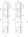
图1是实施例1的光学器件1的构造图。FIG. 1 is a configuration diagram of an
图2是实施例1的光学装置100的构造剖面图。FIG. 2 is a cross-sectional view showing the structure of the
图3是实施例1的光学器件1的制造工序剖面图。FIG. 3 is a cross-sectional view of the manufacturing process of the
图4是实施例1的光学器件1的部分制造工序剖面图。4 is a cross-sectional view of a part of the manufacturing process of the
图5是实施例2的光学装置200的构造剖面图。FIG. 5 is a cross-sectional view showing the structure of an
图6是实施例2的光学装置200的制造工序部分的剖面图。FIG. 6 is a cross-sectional view of part of the manufacturing process of the
图7是实施例3的光学装置300的构造剖面图。FIG. 7 is a cross-sectional view showing the structure of an
图8是现有的半导体装置的构造剖面图。FIG. 8 is a cross-sectional view showing the structure of a conventional semiconductor device.
符号说明Symbol Description
1-光学器件、2-开口部、5-光学元件芯片、5a-光学元件形成面、6-透光性构件、10-器件基板、12-导电部、14-组装、100,200,300-光学器件、101,201,301-布线基板、101a-容纳部(凹部)、201a-容纳部(贯通孔部)、202-密封剂、303-半导体元件芯片1-Optical device, 2-Opening portion, 5-Optical element chip, 5a-Optical element forming surface, 6-Translucent member, 10-Device substrate, 12-Conductive part, 14-Assembly, 100,200,300-Optical device, 101,201,301 -Wiring board, 101a-accommodating portion (recess), 201a-accommodating portion (through-hole portion), 202-sealant, 303-semiconductor element chip
具体实施方式Detailed ways
以下,参照附图详细说明本发明的实施例。并且,本发明并不限于以下所示实施例。Hereinafter, embodiments of the present invention will be described in detail with reference to the drawings. Also, the present invention is not limited to the Examples shown below.
(第1实施例)(first embodiment)
第1实施例中,以图1、图2、图3及图4说明光学器件1的构造、光学装置100的构造、以及光学器件1的制造方法和光学装置100的制造方法。并且,图1是光学器件1的构造图,图2是光学装置100的构造剖面图,图3是光学器件1的制造工序剖面图,图4是光学器件1的一部分制造工序剖面图。并且,图1(b)是光学器件1的背面图,图1(a)是图1(b)的IA-IA线的剖面图。In the first embodiment, the structure of the
-光学器件1的构造和光学装置100的构造--Configuration of
首先说明光学器件1的构造。First, the configuration of the
本实施例的光学器件1如图1所示,包括:形成对表面实质垂直延伸且贯通的开口部2的器件基板10,覆盖所述开口部2的第1开口的透光性构件6,以及覆盖所述开口部的第2开口并形成发射光或接收光的光学元件的光学元件芯片5。并且,光学元件芯片5具备形成光学元件的面(以下称“光学元件形成面”)5a;光学元件芯片5在配置上是光学元件形成面5a和透光性构件6相对形成。光学器件1还进一步具备和光学元件电连接的导电部12。并且,光学元件芯片5和开口部2的周端部之间的空隙以第1密封树脂(密封剂)7加以密封,并且,透光性构件6和开口部2的周端部之间的空隙以第2密封树脂15加以密封。The
器件基板10由环氧树脂等可塑性树脂或由陶瓷等构成。并且,在器件基板10形成有定位孔10a,该定位孔成为决定光学器件1的X·Y方向中心位置的基准,在后述的光学器件1的制造工序中安装光学元件芯片5的基准位置、或对光学器件安装容纳透镜等光学系镜筒时作为镜筒的安装位置基准加以利用。这里,这个定位孔10a只要有2处以上便能够得知光学器件1的中心位置,因此定位孔10a最好是有2处以上。The
透光性构件6是由透过70%以上的光的构件、最好是透过80%以上的光的构件、更好是由透过90%以上的光的构件所构成。例如,玻璃、透明塑胶等。The
在光学元件芯片5形成有CCD等固态影像元件、多个的受光元件离散性配置的元件、和发光元件的其中之一的光学元件。并且,光学元件形成面5a和透光性构件6相对。因此,若是光学元件是发射光的元件,从该光学元件所发射的光通过器件基板10的开口部2穿透透光性构件6发射到光学器件1外部。并且,若是光学元件是受光元件,在光学元件所接收的光是穿过透光性构件6发射到光学器件1、通过器件基板10的开口部2、并在光学元件来接收。On the
并且,光学元件形成面5a的外周部和电极垫5b电连接,电极垫5b表面和凸部(突起电极)8电连接。In addition, the outer peripheral portion of the optical
导电部12,由被埋入到器件基板内部的埋入部和从埋入部延伸并露出于器件基板10的端子部所构成。埋入部由和器件基板10的表面大体平行延伸所设的导电主干部、以及从导电部以接近光学元件芯片5的方向(接近第2开口的方向)延伸而设的导电分支部所构成。导电分支部由内侧导电分支部12a和外侧导电分支部12b所构成,按照这个顺序从远离开口部2的位置而设。内侧导电分支部12a的一端及外侧导电分支部12b的一端如前所述和导电主干部成为一体,内侧导电分支部12a的另一端和凸部8电连接。The
并且,外侧导电分支部12b的另一端,露出于器件基板10外部。换句话说,外侧导电分支部12b的另一端是导电部12的端子部,并且是和后述的布线基板101直接组装的组装部14。这样地,由于光学器件1具备了组装部14,将光学器件1组装到后述的布线基板101上,将能够使光学装置100薄型化。In addition, the other end of the outer
并且,如上所述,以第1密封树脂7将光学元件芯片5和开口部2的周端部之间的空隙加以密封,通过上述使得光学元件和导电部12的电连接部被密封。并且,以第2密封树脂15将透光性构件6和开口部2的周端部之间的空隙加以密封。通过上述,不必要的光侵入到光学器件1内部的可能性极低。并且,第1密封树脂7将光学元件芯片5固定到器件基板10,第2密封树脂15将透光性构件6固定到器件基板10。Furthermore, as described above, the gap between the
其次,说明光学装置100的构造。Next, the structure of the
在本实施例的光学装置100,如图2所示,具备所述光学器件1、和表面形成由凹部构成的容纳部101a的布线基板101。并且,在容纳部101a容纳有光学元件芯片5等。并且,光学器件1的组装部14被直接组装到布线基板101表面,具体而言,即是组装部14和布线基板101通过导电性连接构件61而电连接。这时,导电性连接构件61的量,最好是用来将组装部14和布线基板101电连接的最低限度的量。In the
近几年,摄像机、数码相机、数码静物照相机等被要求薄型化,因此也要求所内藏的光学器件和光学装置的薄型化。In recent years, video cameras, digital cameras, digital still cameras, etc. have been required to be thinner, and therefore, optical devices and optical devices incorporated in them have also been required to be thinner.
一般而言,摄像机、数码相机、数码静物照相机等,锡球被电连接到组装部光学器件(以下称“现有的光学器件”),大体平板状的布线基板将被组装到光学装置(以下称“现有的光学装置”)。但是,这些现有的光学装置由于多了锡球直径部分的额外高度。并且,设置锡球的理由之一在于为了使光学元件芯片设置时远离布线基板表面,因此也无法使锡球直径变小。因此,现有的光学装置中,最大厚度大于现有的光学器件的最大厚度和布线基板的最大厚度之和。因此,难以降低现有光学装置的厚度。In general, for video cameras, digital cameras, digital still cameras, etc., solder balls are electrically connected to the optical device of the assembly part (hereinafter referred to as "existing optical device"), and a substantially flat-shaped wiring board is assembled to the optical device (hereinafter referred to as "existing optical device"). referred to as "existing optical devices"). However, these existing optical devices suffer from the extra height of the diameter of the solder ball. Furthermore, one of the reasons for providing the solder balls is to keep the optical element chip away from the surface of the wiring substrate when the optical element chip is installed, so the diameter of the solder balls cannot be reduced. Therefore, in the conventional optical device, the maximum thickness is greater than the sum of the maximum thickness of the conventional optical device and the maximum thickness of the wiring board. Therefore, it is difficult to reduce the thickness of existing optical devices.
另一方面,如前所述,本实施例的光学器件1,具备直接组装到布线基板101的组装部14。换句话说,光学器件1的外侧导电分支部12b的另一端并未设置锡球。因此,若使用光学器件1,和现有的光学装置相比,能够制造不具有锡球直径的额外高度的光学装置。因此,光学器件1是能够降低光学装置厚度的光学器件。On the other hand, as described above, the
并且,组装有这个光学器件1的布线基板101具备了容纳部101a,容纳部101a容纳有光学元件芯片5等。因此,光学装置100的最大厚度小于光学器件1的最大厚度和布线基板101的最大厚度之和。通过上述,光学装置100能够降低现有光学装置的厚度。具体而言,能够使光学装置100的厚度在0.2mm以上0.8mm以下的范围内。通过上述,若将这个光学器件1及光学装置100内藏到摄像机等,将能够降低摄像机等的厚度。And, the wiring substrate 101 on which this
进一步地,如前所述,在本实施例的光学器件1中,能够阻止不必要的光侵入。因此,若光学元件是受光元件,能够使用在该光学元件所接收的光正确进行影像处理等的分析。并且,由于侵入到光学器件1的不必要的光会在光学元件表面等被反射而不会被发射到光学器件1的外部,若是光学元件是发射光的元件,能够仅将所要的光发射到光学器件1的外部。因此和安装了特开平10-135397号公报中记载的半导体元件的半导体装置相比,本实施例的光学器件1显示了出色的影像处理精度,并能够发射具有所要的特性的光。Further, as described above, in the
并且,本实施例的光学装置100中,容纳部101a周围的布线基板作为光阻止构件产生作用。因此,和特开平10-135397号公报所记载的半导体装置相比,本实施例的光学装置100能够显示出色的影像处理精度等、发射具有所要特性的光。Furthermore, in the
并且,由于组装有光学器件1的布线基板101具备了容纳部101a,和现有的光学装置相同的,光学元件芯片5能够设在远离布线基板101的表面。Furthermore, since the wiring substrate 101 on which the
-光学器件1的制造工序--Manufacturing process of the optical device 1-
首先,在图3(a)所示工序中,将形成布线图案的引线框架(leadframe)安装于密封带20上。这时,构造上,引线框架52的大部分下方设置由半蚀刻或压印所形成的凹部,只有成为内侧导电分支部12a及成为外侧导电分支部12b的部分从凹部底面突出到下方。通过上述,形成在密封带上安装有引线框架52所构成的引线框架构件。并且,这个引线框架52成为所述的导电部12。First, in the process shown in FIG. 3( a ), a lead frame on which a wiring pattern is formed is attached to the sealing
其次,在图3(b)所示工序进行造模工序。这个工序的详细如图4(a)及图4(b)所示。这个工序首先将所述引线框架安装于模具30。这时,图4(a)中造模模具30虽然被显示是一整体构件,但是,是由大体平板形所组成的下方模具和覆盖下方模具的上方模具所构成。并且,上方模具包括30a、30b、和30c;30a是在其中1个表面所形成的2个刚模穴(dieCavity),30b是隔开各刚模穴30a之间的分隔部,30c是在各刚模穴背面分别设置的引脚构件。这里,分隔部30b是成为开口部2的部分,引脚构件30c是成为各个定位孔10a的部分。并且,使引线框架52在上、将所述引线框架构件设置在下方模具的表面,使形成刚模穴30a的面朝下,并且设置上方模具使其覆盖引线框架构件。其次,如图4(b)所示,将环氧树脂等可塑性树脂填充到造模模具30的刚模穴30a。这时,可塑性树脂并未填充到分隔部30b和引脚构件30c。并且,如果可塑性树脂固定后拆离造模模具,从引线框架构件剥离密封带20。通过上述,形成由埋入引线框架52所构成的造模50。这时,内侧导电分支部12a的一部分及外侧导电分支部12b的一部分露出,外侧导电分支部12b露出的部分是组装部14。并且,在内侧导电分支部12a露出的部分,如后述图3(d)所示工序中设置凸部8等。Next, a modeling step is performed in the step shown in FIG. 3( b ). The details of this process are shown in Fig. 4(a) and Fig. 4(b). This process first mounts the lead frame on the
接着,在如图3(C)所示工序将造模50上下颠倒。Next, in the process shown in FIG. 3(C), the
并且,虽然在附图中省略,以刀片(blade)切入和造模相邻接的光学器件形成区域的边界部分在切入部中央部分加以切断将造模50分割成各个光学器件。通过上述,形成由布线12埋入构成的器件基板10。Also, although omitted in the drawings, the
其后,在图3(d)所示工序中,使光学元件芯片5的光学元件形成面5a在下,安装光学元件芯片5来覆盖组装部14所存在的一面的开口(第2开口)。这时,在内侧导电分支部12a的露出部分(内侧导电分支部12a)上设置凸部8,在凸部8上设置光学元件芯片5的电极垫5b、将凸部8和电极垫5b以倒装芯片连接。并且,设置光学元件芯片5时,以设在器件基板10的定位孔10a为基准进行光学元件芯片5的定位,将能够对器件基板10即光学器件1在所要方向设置光学元件芯片5。Thereafter, in the step shown in FIG. At this time, the
接着,在图3(e)所示工序中,使用第1密封树脂7密封内侧导电分支部12a、凸部8及电极垫5b。通过上述,使光学元件和导电部12的电连接部被密封。换句话说,以第1密封树脂7密封光学元件芯片5和开口部2的周端部之间的空隙。Next, in the step shown in FIG. 3( e ), the inner
并且,在图3(f)所示工序中,使图3(e)所示工序被形成的造模上下颠倒设置并覆盖开口部2未被覆盖的一侧的开口(第1开口)安装透光性构件6。并且,使用第2密封树脂15来密封透光性构件6和开口部2的周端部之间的空隙。通过上述制造光学器件1。And, in the process shown in FIG. 3( f), the mold formed in the process shown in FIG. 3( e) is set upside down and covers the opening (first opening) on the side where the
其后,虽然在附图中省略,将光学器件1组装到具备了由凹部形成的容纳部101a的布线基板101。这时,使光学器件1的发光元件芯片5等容纳到容纳部101a,同时使用焊锡等导电性连接构件61将组装部14和布线基板101电连接。通过上述制造光学装置100。Thereafter, although omitted in the drawings, the
并且,由于光学器件1没有具备锡球,和现有的光学器件相比,能够抑制光学器件1的制造成本并能缩短光学器件1的制造时间。相同地,和现有光学装置相比,能够降低光学装置100的制造成本同时能够缩短光学装置100的制造时间。Moreover, since the
(第2实施例)(second embodiment)
第2实施例中,使用图5及图6来说明光学装置200的构造和光学装置200的制造方法。并且,图5是光学装置200的构造剖面图,图6是光学装置200的制造工序剖面图,这些剖面图是图1(b)的IA-IA线的剖面图。In the second embodiment, the structure of the
本实施例的光学器件和所述实施例1的光学器件1大体相同。因此这里省略光学器件的构造及省略制造方法的说明。The optical device of this embodiment is substantially the same as the
-光学装置200的构造--Structure of Optical Device 200-
本实施例的光学装置200,如图5所示,包括:所述实施例1的光学器件,以及形成由贯通孔部构成的容纳部201a(图6(a)所示)的布线基板201。并且,容纳部201a容纳有光学元件芯片5等,同时以密封剂(贯通孔部密封剂)202加以密封。这样地,通过使用密封剂202密封容纳部201a,光学元件芯片5被固定在容纳部201a内,而且,将不会产生不必要的光通过容纳部201a侵入到光学装置200内部。换句话说,本实施例中,密封剂202是光阻止构件。并且,光学装置200中,和所述实施例1的光学装置100相同,通过导电性连接构件61将组装部14和布线基板201电连接。An
-光学装置200的制造工序--Manufacturing process of the optical device 200-
首先,如图6(a)所示工序中,在具备由贯通孔部构成的容纳部201a的布线基板201,组装以所述实施例1记载的制造工序所制造的光学器件1。这时,在容纳部201a容纳光学元件芯片5等。并且,使用导电性连接构件61来使光学器件1的组装部14和布线基板201电连接。并且,组装部14,涂上用来将光学器件1组装到布线基板201上所需要的量的导电性连接构件61。First, in the process shown in FIG. 6( a ), the
并且,在图6(b)所示工序中,密封由贯通孔部构成的容纳部201a。这时,使容纳部201a在上,使用从喷嘴75所供给的密封剂202密封容纳部201a。通过上述,能够制造在本实施例的光学装置200。And, in the step shown in FIG. 6( b ), the
在本实施例的光学装置200和在所述实施例1的光学装置100的不同仅在于:布线基板的容纳部的形状。在所述实施例1中,必须在布线基板101形成厚度厚于光学元件芯片5的容纳部101a。另一方面,布线基板201中,通过在表面设置贯通孔部而形成容纳部201a,因此布线基板201可以厚于光学元件芯片5,也可以是光学元件芯片5厚于布线基板201。根据上述,光学装置200比光学装置100容易设计。The
(第3实施例)(third embodiment)
第3实施例中,使用图7来说明光学装置300的构造和光学装置300的制造方法。并且,图7是光学装置300的构造剖面图,这个剖面图是图1(b)IA-IA线的剖面图。In the third embodiment, the structure of the
本实施例的光学器件和所述实施例1的光学器件1大体相同。因此,这里省略光学器件的构造及制造方法的说明。The optical device of this embodiment is substantially the same as the
-光学装置300的构造--Structure of Optical Device 300-
在本实施例的光学装置300,如图7所示,包括:所述实施例1的光学器件,以及形成由凹部所构成的容纳部(附图省略)的布线基板301。并且,这个容纳部容纳了光学元件芯片5和DSP等半导体元件芯片303,以密封剂(容纳部密封剂)202加以密封。这里,在容纳部表面设置多处的布线302,302,…,在半导体元件芯片303表面设置多处的布线303a…。并且,容纳部的各布线302和半导体元件芯片303的各布线303a,分别以引线连接或倒装芯片连接等电连接。并且,由于光学元件芯片5被容纳在容纳部而且被以密封剂202密封,因此不必要的光侵入了到光学装置300的可能性极低。换句话说,本实施例中,容纳部周围的布线基板和密封剂202是光阻止构件。并且,光学装置300中,和所述实施例1的光学装置100相同的,透过导电性连接构件61将组装部14和布线基板301电连接。An
-光学装置300的制造工序--Manufacturing process of the optical device 300-
虽然在附图中予以省略,首先,将半导体元件芯片303组装到具备由贯通孔部构成的容纳部的布线基板301。这时,分别将半导体元件芯片303的各布线303a和容纳部的各布线302电连接,将半导体元件芯片303容纳到容纳部。Although it is omitted in the drawing, first, the
其次,以密封剂202密封容纳部。通过上述,在容纳部内固定半导体元件芯片303。Next, the accommodating portion is sealed with a
接着,将以所述实施例1记载的方法所制造的光学器件组装到布线基板301。这时,在组装部14涂上必要最低量的导电性连接构件61,同时在密封容纳部的密封剂202表面上安装光学元件芯片5而将光学器件组装到布线基板301。通过上述,将光学元件芯片5容纳到容纳部,能够制造本实施例的光学装置300。Next, the optical device manufactured by the method described in the first embodiment was assembled on the
由于本实施例的光学装置300内藏DSP作为半导体元件芯片303,和所述实施例1及实施例2的光学装置100、200相比,能够高速进行影像处理等。Since the
(其他实施例)(other embodiments)
本发明中有关所述实施例1、实施例2及实施例3,可以是如下构成。In the present invention, the
可以在器件基板10外周部设置定位用阶差部来取代器件基板10所设的定位孔10a。这个定位用的阶差部和定位孔10a具有大体相同的功能。Instead of the
并且,光学器件1的制造工序中,也可以将图3(e)所示光学元件芯片5安装到器件基板10之后分割成各个光学器件,或者是将如图3(f)所示透光性构件6安装到器件基板10之后分割成各个光学器件。In addition, in the manufacturing process of the
并且,最好是,在器件基板10和布线基板101之间的空隙也可以设密封树脂。若这个空隙设密封树脂,由于能够完全阻止不必要的光侵入到光学装置100内,所以比较理想。Also, preferably, a sealing resin may be provided in the gap between the
并且,光学器件1的制造工序中的造模工序,是在将引线框架52安装到密封带的状态,但是并非一定必须使用密封带20。若使用密封带20时,上方模具和下方模具上下钳住引线框架52,能够使得模具和引线框架的上下面密合状态稳定。换句话说,能够使得模具面和引线框架的上下面密合的状态来填充可塑性树脂。结果,能够抑制造模时造成的树脂外露,同时能够容易获得组装部14外露于器件基板10的构造使得将光学器件安装到布线基板时的焊锡连接变得容易等,而使组装简单化、迅速化。In addition, the molding process in the manufacturing process of the
本发明中,有关所述实施例3可以如下构成。In the present invention, the third embodiment can be configured as follows.
半导体元件芯片303可以被封装设置在容纳部内,也可以不被封装的设置到容纳部内。并且,半导体元件芯片303可以是电源IC或周边部件。The
产业上利用的可能性Possibility of industrial use
如上述说明,本发明中,例如对于具备形成有发射光或接收光的光学元件的光学元件芯片的光学器件以及具备该光学器件的光学装置等非常有用。As described above, the present invention is very useful, for example, for an optical device including an optical element chip on which an optical element for emitting or receiving light is formed, and an optical device including the optical device.
Claims (11)
Applications Claiming Priority (2)
| Application Number | Priority Date | Filing Date | Title |
|---|---|---|---|
| JP2004337317 | 2004-11-22 | ||
| JP2004337317AJP4196937B2 (en) | 2004-11-22 | 2004-11-22 | Optical device |
Publications (2)
| Publication Number | Publication Date |
|---|---|
| CN1783503A CN1783503A (en) | 2006-06-07 |
| CN100502019Ctrue CN100502019C (en) | 2009-06-17 |
Family
ID=36461010
Family Applications (1)
| Application Number | Title | Priority Date | Filing Date |
|---|---|---|---|
| CNB2005101186314AExpired - Fee RelatedCN100502019C (en) | 2004-11-22 | 2005-11-01 | optical device |
Country Status (5)
| Country | Link |
|---|---|
| US (1) | US7302125B2 (en) |
| JP (1) | JP4196937B2 (en) |
| KR (1) | KR20060056851A (en) |
| CN (1) | CN100502019C (en) |
| TW (1) | TW200618267A (en) |
Families Citing this family (8)
| Publication number | Priority date | Publication date | Assignee | Title |
|---|---|---|---|---|
| TWI394432B (en)* | 2006-11-27 | 2013-04-21 | Hon Hai Prec Ind Co Ltd | Digital camera modules and method of manufacturing the same |
| TW200904159A (en)* | 2007-07-06 | 2009-01-16 | Kye Systems Corp | Thin type image capturing module |
| US8138027B2 (en)* | 2008-03-07 | 2012-03-20 | Stats Chippac, Ltd. | Optical semiconductor device having pre-molded leadframe with window and method therefor |
| CN102379039B (en)* | 2009-11-26 | 2015-04-01 | 京瓷株式会社 | Wiring board, imaging device, and imaging device module |
| EP2587793B1 (en)* | 2010-06-28 | 2020-01-08 | Kyocera Corporation | Image pickup device and image-pickup device module |
| CN103765865A (en)* | 2011-08-19 | 2014-04-30 | 富士胶片株式会社 | Imaging element module and method for manufacturing same |
| JP6325975B2 (en)* | 2014-12-19 | 2018-05-16 | 新光電気工業株式会社 | Lead frame, semiconductor device |
| KR102756555B1 (en)* | 2022-06-30 | 2025-01-21 | 주식회사 아이윈플러스 | Photo sensor package module |
Family Cites Families (9)
| Publication number | Priority date | Publication date | Assignee | Title |
|---|---|---|---|---|
| JPH11164209A (en)* | 1997-11-25 | 1999-06-18 | Toshiba Corp | Mounting device for solid-state imaging device |
| JP4244096B2 (en)* | 2000-04-14 | 2009-03-25 | パナソニック株式会社 | Semiconductor device and manufacturing method thereof |
| JP2002289749A (en)* | 2001-03-28 | 2002-10-04 | Hitachi Metals Ltd | Wiring board for mounting semiconductor device and semiconductor device mounting package using the same |
| JP2002299592A (en)* | 2001-03-29 | 2002-10-11 | Sony Corp | Semiconductor device |
| US6512861B2 (en)* | 2001-06-26 | 2003-01-28 | Intel Corporation | Packaging and assembly method for optical coupling |
| JP2003303946A (en)* | 2002-04-12 | 2003-10-24 | Sony Corp | Solid-state image pickup device and manufacturing method thereof |
| JP3932279B2 (en)* | 2002-11-13 | 2007-06-20 | 株式会社リコー | Mounting structure, optical sensor module and optical sensor module mounting structure |
| JP4160851B2 (en)* | 2003-03-31 | 2008-10-08 | 富士通株式会社 | Semiconductor device for fingerprint recognition |
| JP3729817B2 (en)* | 2003-04-28 | 2005-12-21 | 松下電器産業株式会社 | Method for manufacturing solid-state imaging device |
- 2004
- 2004-11-22JPJP2004337317Apatent/JP4196937B2/ennot_activeExpired - Fee Related
- 2005
- 2005-10-28USUS11/260,175patent/US7302125B2/ennot_activeExpired - Fee Related
- 2005-10-31KRKR1020050102978Apatent/KR20060056851A/ennot_activeWithdrawn
- 2005-11-01CNCNB2005101186314Apatent/CN100502019C/ennot_activeExpired - Fee Related
- 2005-11-17TWTW094140462Apatent/TW200618267A/enunknown
Also Published As
| Publication number | Publication date |
|---|---|
| KR20060056851A (en) | 2006-05-25 |
| TW200618267A (en) | 2006-06-01 |
| CN1783503A (en) | 2006-06-07 |
| US20060110097A1 (en) | 2006-05-25 |
| US7302125B2 (en) | 2007-11-27 |
| JP4196937B2 (en) | 2008-12-17 |
| JP2006147916A (en) | 2006-06-08 |
Similar Documents
| Publication | Publication Date | Title |
|---|---|---|
| KR100459347B1 (en) | Optic semiconductor device and optic semiconductor module mounting optic semiconductor device | |
| US6550982B2 (en) | Optoelectronic surface-mountable module and optoelectronic coupling unit | |
| CN100420027C (en) | Optical device and manufacturing method thereof | |
| JP4606063B2 (en) | Optical device and manufacturing method thereof | |
| US8077248B2 (en) | Optical device and production method thereof | |
| US8120128B2 (en) | Optical device | |
| CN108293088A (en) | Optical device and method for manufacturing optical device | |
| CN101569023A (en) | Housing for an optoelectronic component and arrangement of the optoelectronic component in the housing | |
| CN107078194A (en) | LED components | |
| JP2010114141A (en) | Light reception/light emission integrated type semiconductor device, and electronic equipment | |
| CN100502019C (en) | optical device | |
| JP2010252164A (en) | Solid-state imaging device | |
| CN101241920A (en) | Optical device and manufacturing method thereof | |
| JP2007242692A (en) | Optical device and method of manufacturing optical device | |
| JP2009111334A (en) | Optical device, manufacturing method thereof, and semiconductor device | |
| KR20050027016A (en) | Semiconductor device and manufacturing method thereof | |
| JP4444931B2 (en) | Optical device manufacturing method | |
| WO2018030261A1 (en) | Optical communication module | |
| JP4301588B2 (en) | Photocoupler device | |
| JP2002185022A (en) | Infrared ray data communication module and manufacturing method therefor | |
| JPH11330539A (en) | Optical semiconductor device | |
| JP2007035725A (en) | Photoelectric conversion module | |
| JP2001077407A (en) | Infrared transmission/reception module and manufacture thereof | |
| JP2000124478A (en) | Optical semiconductor device | |
| JP2000004067A (en) | Optical semiconductor device and optical semiconductor module mounted with the same |
Legal Events
| Date | Code | Title | Description |
|---|---|---|---|
| C06 | Publication | ||
| PB01 | Publication | ||
| C10 | Entry into substantive examination | ||
| SE01 | Entry into force of request for substantive examination | ||
| C14 | Grant of patent or utility model | ||
| GR01 | Patent grant | ||
| C17 | Cessation of patent right | ||
| CF01 | Termination of patent right due to non-payment of annual fee | Granted publication date:20090617 Termination date:20101101 |