CN100487673C - Secondary memory device and method for using secondary memory - Google Patents
Secondary memory device and method for using secondary memoryDownload PDFInfo
- Publication number
- CN100487673C CN100487673CCNB2005100734650ACN200510073465ACN100487673CCN 100487673 CCN100487673 CCN 100487673CCN B2005100734650 ACNB2005100734650 ACN B2005100734650ACN 200510073465 ACN200510073465 ACN 200510073465ACN 100487673 CCN100487673 CCN 100487673C
- Authority
- CN
- China
- Prior art keywords
- memory
- logical addresses
- secondary memory
- degraded
- memory controller
- Prior art date
- Legal status (The legal status is an assumption and is not a legal conclusion. Google has not performed a legal analysis and makes no representation as to the accuracy of the status listed.)
- Expired - Fee Related
Links
- 230000015654memoryEffects0.000titleclaimsabstractdescription313
- 238000000034methodMethods0.000titleclaimsabstractdescription45
- 230000002950deficientEffects0.000claimsabstractdescription12
- 238000005520cutting processMethods0.000claimsdescription42
- 238000004806packaging method and processMethods0.000claimsdescription5
- 230000015556catabolic processEffects0.000abstractdescription4
- 238000006731degradation reactionMethods0.000abstractdescription4
- 238000010586diagramMethods0.000description21
- 230000007547defectEffects0.000description9
- 238000013461designMethods0.000description9
- 238000005516engineering processMethods0.000description7
- 238000012360testing methodMethods0.000description5
- 238000006243chemical reactionMethods0.000description4
- 238000013507mappingMethods0.000description4
- 230000011218segmentationEffects0.000description4
- 230000008901benefitEffects0.000description3
- 230000006870functionEffects0.000description3
- 238000011017operating methodMethods0.000description2
- 230000008439repair processEffects0.000description2
- 238000013519translationMethods0.000description2
- ROXBGBWUWZTYLZ-UHFFFAOYSA-N[6-[[10-formyl-5,14-dihydroxy-13-methyl-17-(5-oxo-2h-furan-3-yl)-2,3,4,6,7,8,9,11,12,15,16,17-dodecahydro-1h-cyclopenta[a]phenanthren-3-yl]oxy]-4-methoxy-2-methyloxan-3-yl] 4-[2-(4-azido-3-iodophenyl)ethylamino]-4-oxobutanoateChemical compoundO1C(C)C(OC(=O)CCC(=O)NCCC=2C=C(I)C(N=[N+]=[N-])=CC=2)C(OC)CC1OC(CC1(O)CCC2C3(O)CC4)CCC1(C=O)C2CCC3(C)C4C1=CC(=O)OC1ROXBGBWUWZTYLZ-UHFFFAOYSA-N0.000description1
- 230000008859changeEffects0.000description1
- 238000009826distributionMethods0.000description1
- 230000000694effectsEffects0.000description1
- 230000010354integrationEffects0.000description1
- 230000009191jumpingEffects0.000description1
- 238000004519manufacturing processMethods0.000description1
- 230000008569processEffects0.000description1
- 239000004065semiconductorSubstances0.000description1
- 238000004088simulationMethods0.000description1
Images


Landscapes
- Dram (AREA)
- Techniques For Improving Reliability Of Storages (AREA)
Abstract
Description
Translated fromChinese技术领域technical field
本发明涉及一种内存控制器及其操作方法,尤其涉及一种可使用次级(downgrade)内存并对其做初始化的内存控制器及其操作方法。The present invention relates to a memory controller and its operating method, in particular to a memory controller capable of using and initializing a downgrade memory and its operating method.
背景技术Background technique
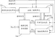
图1为一般DDR SDRAM内存的方框图,从SDRAM开始的主流DRAM皆具有类似结构。该内存被划分为多个记忆槽(Bank),每个记忆槽通过槽地址来选取,而记忆槽中的数据可以通过多个行(column)地址及列(row)地址来加以选择存取。如图1所示,随着内存容量的逐渐增大以及为了配合内存内部结构的设置,行地址及列地址一般以多任务的方式进行选择。以256M的32M*8内存为例,即,将图1左上侧的总线A0-A12分配给列地址,而其中有部分总线(如A0-A9)按照命令的不同被分配给行地址,因此可以达到节省管脚的目的。如图1所示,该内存的总线还包括:用以选择记忆槽的记忆槽地址BA0、BA1,在图1左下侧的控制信号线/CAS、/RAS、/WE及/CS(斜线“/”代表反相信号),右下侧的数据输出和输入信号线DQ0-DQ7。此外,地址总线BA0、BA1和A0-A12除了用于寻址外,还用于模式寄存器(Mode Registers)的设定。Figure 1 is a block diagram of a general DDR SDRAM memory. The mainstream DRAM starting from SDRAM has a similar structure. The memory is divided into multiple memory slots (Bank), and each memory slot is selected by a bank address, and the data in the memory slot can be selectively accessed by multiple row (column) addresses and column (row) addresses. As shown in Figure 1, with the gradual increase of the memory capacity and in order to cooperate with the setting of the internal structure of the memory, the row address and the column address are generally selected in a multi-task manner. Take the 256M 32M*8 memory as an example, that is, assign the bus A0-A12 on the upper left side of Figure 1 to the column address, and some of the buses (such as A0-A9) are assigned to the row address according to different commands, so you can To achieve the purpose of saving pins. As shown in Figure 1, the bus of the memory also includes: memory slot addresses BA0 and BA1 for selecting memory slots, control signal lines /CAS, /RAS, /WE and /CS on the lower left side of Figure 1 (slash " /"represents the inverted signal), the data output and input signal lines DQ0-DQ7 on the lower right side. In addition, the address buses BA0, BA1 and A0-A12 are not only used for addressing, but also used for setting of mode registers (Mode Registers).
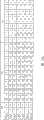
图2为标准SDRAM内存的内存大小与行地址、列地址及记忆槽地址(Bank address)的分配关系图。以256M的32M*8结构的内存为例,如图2所示,其槽地址、列地址、行地址被设定为(2,13,10)。从图2的标准内存的地址配置可以看出,为了使内存控制器能正确存取公知的内存,内存控制器和内存在各个地址的管脚数目被规范化。Figure 2 is a diagram of the distribution relationship between the memory size of the standard SDRAM memory and the row address, column address and memory slot address (Bank address). Taking a 256M memory with a 32M*8 structure as an example, as shown in FIG. 2 , its slot address, column address, and row address are set to (2, 13, 10). It can be seen from the address configuration of the standard memory in FIG. 2 that in order to enable the memory controller to correctly access the known memory, the number of pins at each address of the memory controller and the memory is standardized.
随着半导体技术的进步,内存的容量也大幅提高,早期的计算机一般仅能存取640K的内存,而目前的操作系统已能存取4G以上的内存,因此目前的内存大都在128M以上。一般内存在制作后必须经过一个测试步骤,如果内存的缺陷(defect)不严重,则在封装前可以使用内存上的冗余(redundant)内存来修补;如果内存的缺陷严重,则此内存不能达到标准的规格。对于这种有缺陷的内存,除了丢弃外,也可以作为次级内存使用,即仅使用内存上可正常存取的部分,因此次级内存可使用的记忆容量比正常内存的额定记忆容量小。With the advancement of semiconductor technology, the capacity of memory has also been greatly increased. Early computers can only access 640K of memory, but the current operating system can access more than 4G of memory, so most of the current memory is above 128M. Generally, the memory must go through a test step after production. If the defect of the memory is not serious, the redundant memory on the memory can be used to repair it before packaging; if the defect of the memory is serious, the memory cannot reach Standard specifications. For this kind of defective memory, in addition to being discarded, it can also be used as a secondary memory, that is, only the normally accessible part of the memory is used, so the memory capacity that the secondary memory can use is smaller than the rated memory capacity of the normal memory.
公知的次级内存的使用方式有以下三种方法或者以下三种方法的综合:The known ways of using the secondary memory include the following three methods or a combination of the following three methods:
第一种方法如图3A所示,是以外部冗余内存76来修补次级内存70的错误,这种方法以一个外部非易失性记忆单元72来记录经测试得到的缺陷位置。外部非易失性记忆单元72可利用如EEPROM/Flash实现;而外部冗余内存76可利用如SRAM/DRAM实现,外部冗余内存76可被集成在ASIC内或单独存在。比较与控制单元74对比存取地址是否位于缺陷位置,并根据对比结果来控制数据总线多任务器78,以决定是否由外部冗余内存76来取代输出。该方法的一种变化方式是不使用数据总线多任务器78,而由比较与控制单元74直接控制次级内存70的DM/DQM信号,以达到关闭一方输出的效果。该方法的缺点是成本高,需要高速及复杂的比较与控制单元74,或需要将冗余内存集成在同一ASIC中。此外,不论是使用多任务器还是使用DM/DQM信号拦截在数据总线衍生的数据总线冲突(BusContention),都使该方法在速度上无法提高。再者,如图1所示,由于要在非易失性记忆单元72分别记录经测试得到的错误点的缺陷位置或错误地址区,以及需要考虑比较与控制单元74中的比较器的复杂度等问题,因此该方法仅能适用于缺陷较少或用于对存取速度要求不高的应用中。The first method, as shown in FIG. 3A , uses an external
第二种公知方法是使用数据线切割的方式,即,利用数据线(DQ)来排除有瑕疵的区域使其不予存取。如图3B所示,以32M*8的SDRAM为例,若有两个32M*8的SDRAM经过测试筛选,以每一个32M*1bit DQ线作为一个单元来看,假设测试的结果是该两个32M*8的SDRAM分别具有32M*2(DQ0-DQ1)及32M*6(DQ2-DQ7)的可用区域,则可经由电路板的线路设置将两个SDRAM总共可用的8(2+6)个DQ线拉出即可模拟成一个完整的32M*8的SDRAM来使用。此方法的优点是成本低,但缺点是使用率不够理想,这是因为32M*1bit DQ的单元并不符合内存内部结构的大区域安排,因此有些内存如果仅有微小的瑕疵,却因为某个地址的8个位全坏,而无法用此方法,因此很多有瑕疵的内存不能依此方式作为次级内存使用。The second known method is to use data line cutting, ie, use data lines (DQ) to exclude defective areas from being accessed. As shown in Figure 3B, taking the 32M*8 SDRAM as an example, if two 32M*8 SDRAMs have been tested and screened, each 32M*1bit DQ line is regarded as a unit, assuming that the test result is that the two The 32M*8 SDRAM has available areas of 32M*2 (DQ0-DQ1) and 32M*6 (DQ2-DQ7) respectively, and the total available 8 (2+6) of the two SDRAMs can be set through the circuit board circuit settings. Pull out the DQ line to simulate a complete 32M*8 SDRAM for use. The advantage of this method is that the cost is low, but the disadvantage is that the utilization rate is not ideal. This is because the 32M*1bit DQ unit does not conform to the large area arrangement of the internal structure of the memory. The 8 bits of the address are all broken, and this method cannot be used, so many defective memories cannot be used as secondary memory in this way.
第三种公知方法是使用地址切割的方式,即以地址来排除有瑕疵的区域不予存取。例如32M*8的DRAM(如图2所示,Bank*Row*Column为2*13*10),如果经测试后所有瑕疵的区域都对应在Row地址A12为高(High)的区域内,则可以通过将实体地址线A12变为低(Low)(参见图3C),来排除瑕疵区域并使其不予使用。此时该内存的地址变成Bank*Row*Column为2*12*10,如图2所示,此次级内存符合标准的16M*8DRAM。因为地址的数量多,所以这种地址切割方式可变化种类繁多,且除了High/Low外,还有地址相等/反相等诸多变化可运用。可以降一级、降两级(32M*8降为8M*8)甚至更多级,因此可提高使用率。该方法的缺点是多数运用都需使用ASIC来做地址转换,这是因为若选用的地址所对应的地址线非专用(具有列地址及行地址的多任务功能),或者虽为专用但被简单地置为High/Low后却非标准的内存地址配置,这样必须用AISC做地址转换,举例来说,对于2*12*10的16M*8内存而言,如经测试分类后的结果是将A1l置为Low后才能避免存取瑕疵,但将A11置为Low后却为2*11*10的地址配置。如图2所示,该配置并非标准的内存地址配置,需再经由一特定的ASIC转换成对外部而言为2*12*9的标准型8M*8DRAM。另一个需要使用ASIC的原因是SDRAM及其后继的内存的地址线还被用于初始化的命令用途(MRS,EMRS等命令),因此需使用额外的转换电路。The third known method is to use address segmentation, that is, use addresses to exclude defective areas from being accessed. For example, for a 32M*8 DRAM (as shown in Figure 2, Bank*Row*Column is 2*13*10), if after testing all defective areas correspond to the area where Row address A12 is High (High), then The defective area can be excluded and unused by turning the physical address line A12 to Low (see FIG. 3C ). At this time, the address of the memory becomes Bank*Row*Column to be 2*12*10, as shown in Figure 2, the secondary memory conforms to the standard 16M*8DRAM. Because of the large number of addresses, this address cutting method can be changed in a variety of ways, and in addition to High/Low, there are many changes of address equality/reverse equality that can be used. It can be reduced by one level, two levels (32M*8 to 8M*8) or even more levels, so the utilization rate can be improved. The disadvantage of this method is that most applications need to use ASIC to do address translation. After the address is set to High/Low, it is not a standard memory address configuration, so AISC must be used for address translation. Only after A11 is set to Low can access defects be avoided, but after A11 is set to Low, the address configuration is 2*11*10. As shown in Figure 2, this configuration is not a standard memory address configuration, and needs to be converted into a standard 8M*8DRAM that is 2*12*9 for the outside through a specific ASIC. Another reason for using ASIC is that the address lines of SDRAM and its subsequent memory are also used for initialization commands (MRS, EMRS and other commands), so additional conversion circuits are required.
上述方法在使用ASIC后,除了增加成本,还会造成信号延迟,影响高速应用的可行性。而且,各种不同转换地址方式需不同ASIC电路设计,弹性不足。此外,有些转换需求无法达成,例如只能通过仿真将行地址减少,但不能增加。After the above method uses ASIC, in addition to increasing the cost, it will also cause signal delay and affect the feasibility of high-speed applications. Moreover, various address conversion methods require different ASIC circuit designs, which is insufficient in flexibility. In addition, some conversion requirements cannot be achieved, for example, the row address can only be reduced through simulation, but cannot be increased.
本发明的内容Contents of the invention
上述公知技术在成本、高速应用或在可使用率方面存在上述缺陷。本发明的次级内存装置克服了上述缺陷,并具有成本低、使用率高的优点,并且几乎没有速度延迟。The above-mentioned known techniques have the above-mentioned disadvantages in terms of cost, high-speed application or availability. The secondary memory device of the present invention overcomes the above-mentioned defects, and has the advantages of low cost, high utilization rate, and almost no speed delay.
为了实现本发明的上述目的,本发明提供了一种次级内存装置,用于提供一子系统使用次级内存,所述子系统具有一为m个逻辑地址的内存需求数值,所述次级内存装置包含:一次级内存,具有一含有瑕疵内存区域的降级切割部分,及一完全为正常内存区域的未降级切割部分,所述降级切割部分及所述未降级切割部分皆以次级内存的逻辑地址来界定;In order to achieve the above object of the present invention, the present invention provides a secondary memory device for providing a subsystem using secondary memory, the subsystem has a memory requirement value of m logical addresses, the secondary The memory device comprises: a secondary memory having a degraded cut portion containing a defective memory area, and a non-degraded cut portion which is completely a normal memory area, the degraded cut portion and the non-degraded cut portion are all based on the secondary memory logical address to define;
一内存控制器,连接于所述子系统及所述次级内存之间,其中所述次级内存具有n个逻辑地址,所述n个逻辑地址包含不需所述内存控制器处理的q个逻辑地址及需要所述内存控制器处理的(n-q)=p个逻辑地址,其中所述降级切割部分包含不需所述内存控制器处理的q个逻辑地址和需要所述内存控制器处理的r个逻辑地址,未降级切割部分包括需要所述内存控制器处理的p-r个逻辑地址;及一记录装置,电连接到所述内存控制器,并记录所述次级内存的降级切割设定,所述内存控制器通过连接到所述次级内存的第一数目x的实体地址以对所述次级内存进行初始化,其中第一数目x的实体地址线为所述p个逻辑地址所分布的实体地址线,包括送出设定所述次级内存的列地址选通脉冲时间、包装类型及脉冲时间的信号,降级切割部分的所述r个逻辑地址依照降级切割状态送出适当信号;所述内存控制器可以依据所述记录装置的降级切割设定而选取所述未降级切割部分的p-r个逻辑地址的子集供所述子系统使用,其中p-r大于m,且对于p-r-m未使用的逻辑地址,所述内存控制器送出固定信号,以提供所述子系统的所述内存需求数值。A memory controller, connected between the subsystem and the secondary memory, wherein the secondary memory has n logical addresses, and the n logical addresses include q that do not need to be processed by the memory controller Logical addresses and (n-q)=p logical addresses that need to be processed by the memory controller, wherein the degraded cutting part includes q logical addresses that do not need to be processed by the memory controller and r that need to be processed by the memory controller Logical addresses, the non-degraded cutting part includes p-r logical addresses that need to be processed by the memory controller; and a recording device, electrically connected to the memory controller, and recording the downgraded cutting setting of the secondary memory, so The memory controller initializes the secondary memory by connecting to a first number x of physical addresses of the secondary memory, wherein the first number x of physical address lines are entities distributed by the p logical addresses The address line includes sending signals for setting the column address strobe pulse time, packaging type and pulse time of the secondary memory, and the r logic addresses of the degraded cutting part send appropriate signals according to the degraded cutting state; the memory control The device can select a subset of p-r logical addresses of the non-degraded cut part for use by the subsystem according to the downgraded cutting setting of the recording device, wherein p-r is greater than m, and for p-r-m unused logical addresses, the The memory controller sends a fixed signal to provide the memory requirement value of the subsystem.
本发明同时还提供了一种使用次级内存的方法,可依据一子系统的为m个逻辑地址的内存需求数值以存取一次级内存,所述次级内存具有一含有瑕疵内存区域的降级切割部分,及一完全为正常内存区域的包含p个逻辑地址的未降级切割部分,所述方法包含:提供一内存控制器以连接于所述子系统及所述次级内存之间,其中所述次级内存具有n个逻辑地址,所述n个逻辑地址包含不需所述内存控制器处理的q个逻辑地址及需要所述内存控制器处理的(n-q)=p个逻辑地址,其中所述降级切割部分包含不需所述内存控制器处理的q个逻辑地址和需要所述内存控制器处理的r个逻辑地址,未降级切割部分包括需要所述内存控制器处理的p-r个逻辑地址;设定对于所述次级内存的所需逻辑地址,其中所述所需逻辑地址所决定的内存区域小于未降级切割部分,包括设定在p-r个逻辑地址中选取m个逻辑地址的对应表;通过连接到所述次级内存的第一数目x的实体地址以对所述次级内存进行初始化,其中第一数目x的实体地址线为所述p个逻辑地址所分布的实体地址线,包括送出设定所述次级内存的列地址选通脉冲时间、包装类型及脉冲时间的信号,降级切割部分的所述r个逻辑地址依照降级切割状态送出适当信号;依据所述所需逻辑地址的对应表以存取所述次级内存的部分的未降级切割部分,并对于未使用的p-r-m个逻辑地址送出预定信号,以提供所述子系统的所述内存需求数值。The present invention also provides a method of using secondary memory that can access a secondary memory with a degraded memory region containing a defect based on the memory requirement value of m logical addresses of a subsystem. a segmented part, and a non-degraded segmented part comprising p logical addresses which is completely a normal memory area, the method comprising: providing a memory controller to be connected between the subsystem and the secondary memory, wherein the The secondary memory has n logical addresses, and the n logical addresses include q logical addresses that do not need to be processed by the memory controller and (n-q)=p logical addresses that need to be processed by the memory controller, wherein the The degraded cut part includes q logical addresses that do not need to be processed by the memory controller and r logical addresses that need to be processed by the memory controller, and the non-degraded cut part includes p-r logical addresses that need to be processed by the memory controller; Setting the required logical address for the secondary memory, wherein the memory area determined by the required logical address is smaller than the non-degraded cut part, including setting a corresponding table for selecting m logical addresses from the p-r logical addresses; The secondary memory is initialized by connecting to a first number x of physical addresses of the secondary memory, wherein the first number x of physical address lines are physical address lines distributed by the p logical addresses, including Send out the signal of setting the column address strobe pulse time, packaging type and pulse time of the secondary memory, and the r logical addresses of the degraded cutting part send appropriate signals according to the degraded cutting state; according to the required logical address A table is used to access the non-degraded cut portion of the portion of the secondary memory, and a predetermined signal is sent for unused p-r-m logical addresses to provide the memory requirement value of the subsystem.
绝大多数现有的内存控制器设计都可以很容易引用本发明的方法,而涵盖的切割地址可以包括槽地址、列地址、以及脉冲时间(Burst Length)范围以外的行地址。少数以全页突发(Full Page Burst)模式来存取内存的较简单型内存控制器(例如运用于视频转换的视频帧缓冲存储器的控制器即可能采用此种简单方式),只要次级内存的页大小(Page Size)大于原本需要的页大小,就可以在槽地址、列地址、以及超过原需求的页大小以上的高的行地址上引用本发明的方法,所以本发明在实施上并无困难。Most existing memory controller designs can easily refer to the method of the present invention, and the cutting addresses covered can include slot addresses, column addresses, and row addresses outside the range of the burst length (Burst Length). A small number of simpler memory controllers that access memory in Full Page Burst mode (such as the controller of video frame buffer memory used in video conversion may use this simple method), as long as the secondary memory If the page size (Page Size) is greater than the original required page size, the method of the present invention can be quoted on the slot address, the column address, and the high row address exceeding the page size of the original requirement, so the present invention does not implement No difficulty.
附图的简要说明Brief description of the drawings
图1为一般DDR SDRAM内存的方框图;Figure 1 is a block diagram of a general DDR SDRAM memory;
图2为标准SDRAM内存的内存大小与行地址、列地址及记忆槽地址的分配关系图;Fig. 2 is the memory size of the standard SDRAM memory and the allocation relationship diagram of row address, column address and memory slot address;
图3A为表示公知的一种次级内存使用方式的方框图;FIG. 3A is a block diagram showing a known way of using secondary memory;
图3B为表示公知的另一种次级内存使用方式的方框图;Fig. 3B is a block diagram representing another known secondary memory usage;
图3C为表示公知的另一种次级内存使用方式的方框图;FIG. 3C is a block diagram representing another known secondary memory usage;
图4A为本发明第一优选实施例的示意方框图;Figure 4A is a schematic block diagram of a first preferred embodiment of the present invention;
图4B为本发明第二优选实施例的示意方框图;4B is a schematic block diagram of a second preferred embodiment of the present invention;
图4C为本发明第三优选实施例的示意方框图;Fig. 4C is a schematic block diagram of a third preferred embodiment of the present invention;
图4D为本发明第四优选实施例的示意方框图;4D is a schematic block diagram of a fourth preferred embodiment of the present invention;
图4E为本发明第五优选实施例的示意方框图;Figure 4E is a schematic block diagram of a fifth preferred embodiment of the present invention;
图5为本发明第一优选实施例工作原理的示意图;5 is a schematic diagram of the working principle of the first preferred embodiment of the present invention;
图6为本发明第一优选实施例的操作流程;Fig. 6 is the operation process of the first preferred embodiment of the present invention;
图7A为说明一种可行的前后端映射关系的图;FIG. 7A is a diagram illustrating a feasible front-end and back-end mapping relationship;
图7B为说明另一种可行的前后端映射关系的图;FIG. 7B is a diagram illustrating another feasible front-end and back-end mapping relationship;
图8为说明本发明设计概念的示意图。Fig. 8 is a schematic diagram illustrating the design concept of the present invention.
附图中,各标号所代表的部件列表如下:In the accompanying drawings, the list of parts represented by each label is as follows:
70-内存 72-外部非易失性记忆单元70-Memory 72-External non-volatile memory unit
74-比较与控制单元 76-外部冗余内存74-comparison and control unit 76-external redundant memory
78-数据总线多任务器78 - data bus multiplexer
10-电子系统 20-次级内存10-Electronic system 20-Secondary memory
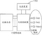
100-子系统 140-记录装置100-subsystem 140-recording device
具体实施方式Detailed ways
为了使本领域技术人员进一步了解本实用新型的特征及技术内容,请参阅以下有关本实用新型的详细说明与附图,附图仅提供参考与说明用,并非用来对本实用新型加以限制。In order for those skilled in the art to further understand the features and technical contents of the present utility model, please refer to the following detailed description and accompanying drawings of the present utility model. The accompanying drawings are provided for reference and illustration only, and are not intended to limit the present utility model.
在任何使用内存的应用系统中,其一或多个子系统要存取内存时,通过一个内存控制器装置来进行。为了后文叙述方便,我们将上述子系统称为内存需求者(Memory Requester),而该内存控制器朝向内存的部分称为前端(Front-End),朝向内存需求者(即,上述子系统)的部分称为后端(Back-End)。内存控制器的功能是多重的,其功能与复杂性根据应用系统而定,但基本上会有内存刷新(Refresh)控制、内存页(Page)的开关控制与追踪、内存初始化控制和建立内存控制器前端与后端的映像关系等等。In any application system using memory, when one or more subsystems want to access the memory, they do so through a memory controller device. For the convenience of the following description, we will refer to the above-mentioned subsystem as the memory requester (Memory Requester), and the part of the memory controller facing the memory is called the front-end (Front-End), facing the memory requester (that is, the above-mentioned subsystem) The part called back-end (Back-End). The functions of the memory controller are multiple, and its function and complexity depend on the application system, but basically there are memory refresh (Refresh) control, memory page (Page) switch control and tracking, memory initialization control and memory establishment control The image relationship between the front end and the back end of the server and so on.
在公知的次级内存运用技术中,将一或多个次级内存仿真成一个标准的内存以供内存控制器连接使用。而本发明对通过以地址切割来进行降级的次级内存,依照其切割方式,在内存控制器内部建立新的初始化控制及前后端映像关系,并在降级的地址上做指定输出,从而达成直接使用通过地址切割后的次级内存的目的。In the known secondary memory utilization technology, one or more secondary memories are emulated as a standard memory for connection and use by a memory controller. However, the present invention establishes a new initialization control and front-end and front-end image relationship inside the memory controller according to the cutting method for the secondary memory that is downgraded by address cutting, and makes a designated output on the downgraded address, so as to achieve direct The purpose of using the secondary memory after cutting by address.
图4A为本发明第一优选实施例的示意方框图,本发明可以应用在任何需要内存的电子系统10中。如图4A所示,电子系统10包括一个或是多个子系统100,子系统100通过内存控制器120来存取次级内存20。FIG. 4A is a schematic block diagram of a first preferred embodiment of the present invention, and the present invention can be applied to any
图5为说明本发明第一优选实施例工作原理的示意图。假设子系统100所需的内存容量在地址部分为2的m次方,也就是有m个逻辑地址。而在地址部分的容量为2的n次方的内存20(其逻辑地址包含了槽地址、列地址及行地址共有n个)在地址切割后的容量大于2的m次方。Fig. 5 is a schematic diagram illustrating the working principle of the first preferred embodiment of the present invention. Assume that the memory capacity required by the
假定其中有分布在y个实体地址线的q个逻辑地址(q大于或等于零)属于降级切割的逻辑地址,且其降级切割和初始化控制命令并不需经过逻辑闸(即,这y个实体地址线可被简单置于high/low或被直接连接到某些信号),则这些地址线可以选择性地不连接到本发明的内存控制器120而直根据降级来被定义。其余(n-q)=p(p>m)个逻辑地址所分布的x个实体地址线则全部连接到该内存控制器120上,而p个逻辑地址中有r(r>0)个降级逻辑地址,而(p-r)≧m,该内存控制器装置120在送出内存初始化命令时,通过连接在其上的x个地址线依照初始化的需求送出正确的信号;在内存存取阶段,则仅利用了子系统100所需的m个未作降级切割的有效逻辑内存,而降级切割用的r个地址则依照降级切割状态来送出适当信号,若存在有超过m个以上的未降级切割的(p-r-m)个有效记忆地址,超过而未使用的部分可送出任意但固定的信号,这样等同于将这(p-r-m)个有效而冗余的地址线视为降级地址使用,从而简化了设计。Assume that q logical addresses (q greater than or equal to zero) distributed on y physical address lines belong to the logical addresses of degraded cutting, and its degraded cutting and initialization control commands do not need to pass through logic gates (that is, these y physical addresses line can be simply set high/low or directly connected to some signal), then these address lines can be selectively not connected to the
图6为本发明第一优选实施例的操作流程图。Fig. 6 is a flowchart of the operation of the first preferred embodiment of the present invention.
步骤S600:决定电子系统所需的逻辑地址数目m并决定连接的内存逻辑地址数目p;Step S600: Determine the number m of logical addresses required by the electronic system and determine the number p of logical addresses of the connected memory;
步骤S610:决定降级切割的逻辑地址数目r;Step S610: Determine the number r of logical addresses for degraded cutting;
步骤S620:依据连接的x个内存实体地址线送出初始化信号;Step S620: sending an initialization signal according to the connected x memory entity address lines;
步骤S630:根据电子系统所需的逻辑地址数目m,存取内存中2的m次方个记忆单元部分;Step S630: According to the number m of logical addresses required by the electronic system,
步骤S640:对于r个降级切割用的地址,依照降级切割状态来送出适当信号;及Step S640: For the r addresses for degraded cutting, send appropriate signals according to the degraded cutting state; and
步骤S650:对于(p-r-m)个未使用的未降级切割的有效内存,送出任意但固定的信号。Step S650: For (p-r-m) unused effective memories that are not degraded and cut, send an arbitrary but fixed signal.
图4B为本发明第二优选实例的示意方框图,为了提高本发明的内存控制器的使用弹性,本发明可以导入辨识用的记录装置140,以使内存控制器120可通过其指示来根据内存20不同的切割降级方式来使用有效逻辑地址、送出正确初始化命令和送出正确的降级状态。Fig. 4B is a schematic block diagram of the second preferred example of the present invention. In order to improve the flexibility of use of the memory controller of the present invention, the present invention can introduce a
记录装置140可以是任何记录型式,例如是跳线(Jumper)或跳接状态的电阻或EEPROM或通过应用系统中的微控制器(Micro-Controller)可读取的任何记录装置。而记录装置140还可用来指示内存控制器120支持不同结构的内存的次级内存,例如为4M*16或8M*16的内存。The
在本发明的第二个实施例中,内存控制器120的后端只有一个需求者微控制器100,假定其需求的记忆容量为8M*16,其连接到内存控制器120的地址线有SA0,SA1...SA22,而前端的内存20选用的是16M*16 SDRAM降级为8M*16的次级内存。该内存20所支持的地址切割形式有以下六种,我们以BA代表槽地址,RA代表列地址,CA表行地址。第一种切割形式是CA7=L的区域为无瑕疵区,第二种为CA7=H的区域为无瑕疵区,第三种为RA7=L的区域为无瑕疵区,第四种为RA7=H的区域为无瑕疵区,第五种为CA7=RA7的区域为无瑕疵区,第六种为CA7=/RA7(斜线代表反相)的区域为无瑕疵区。而内存20的所有实体地址线A0...A12,BA0,BA1连接到内存控制器装置的MA0...MA14管脚。在该实施例的中,记录装置140通过采用三个跳接的跳线JP0-JP2连接到内存控制器装置120的三个输入脚S2,S1和S0来实现。本领域的普通技术人员应该认识到,上述六种地址切割形式的次级内存中,虽有8M*16的可用容量,但却无法通过任何电路仿真成标准的8M*16结构来使用。In the second embodiment of the present invention, there is only one demander
本实施例依照本发明的内存控制器120的运作方式如下:假设内存控制器120固定使用的列地址选通脉冲时间(CAS Latency)=3,包装类型(WrapType)为线性模式(linear Mode),脉冲时间(Burst Length)=4,则在执行内存初始化的MRS命令时,其MA14..MA0送出的信号为0,0,0,0,0,0,0,0,0,1,1,0,0,1,0,也就是MA1,MA4,MA5为High,其余为Low,(此部分的说明可对应于前述的步骤S620)。In this embodiment, the operation mode of the
而在存取命令时,将前端的逻辑地址BA0,1,RA0..RA12,CA0..CA8与后端的SA0,SA1...SA22依照S2,S1,S0的输入状态建立如图7A所示的对应关系或输出状态,由图7A中可以看出,当S2,S1,S0分别为L,L,L时,可支持CA7=L时所确定的次级内存,当S2,S1,S0分别为L,L,H时可支持CA7=H时所确定的次级内存,依此类推(此部分的说明可对应于前述的步骤S630)。When accessing commands, the front-end logical addresses BA0, 1, RA0..RA12, CA0..CA8 and the back-end SA0, SA1...SA22 are established according to the input states of S2, S1, and S0, as shown in Figure 7A Corresponding relationship or output state, as can be seen from Fig. 7A, when S2, S1, S0 are L, L, L respectively, can support the secondary memory determined when CA7=L, when S2, S1, S0 respectively When it is L, L, H, it can support the secondary memory determined when CA7=H, and so on (the description of this part may correspond to the aforementioned step S630).
本发明的第三实施例的电路方框图如图4C所示。在本实施例中,记录装置140进一步增加一个用于辨识的输入脚S3以增加其它的切割方式。在S3为Low时,保持支持原来的6种切割;在S3为High时,则增加了6种新的切割。即S3,S2,S1,S0分别为H,L,L,L时支持CA5=L的切割降级方式;S3,S2,S1,S0分别为H,L,L,H时支持CA5=H的切割降级方式;S3,S2,S1,S0分别为H,L,H,L时支持RA5=L的切割降级方式;S3,S2,S1,S0分别为H,L,H,H时支持RA5=H的切割降级方式;S3,S2,S1,S0分别为H,H,L,L时支持CA5=RA5的切割降级方式;S3,S2,S1,S0分别为H,H,L,H时支持CA5=/RA5的区域为无瑕疵区。本实施例的运作方式如下,在初始化MRS命令时与第一或二实施例相同,而在存取命令时,在S3为Low时与图7A相同,在S3为High时前端与后端的对应关系或输出状态如图7B所示。The circuit block diagram of the third embodiment of the present invention is shown in Fig. 4C. In this embodiment, the
通过上面的描述,本领域的普通技术人员可以很容易看出,在保留根据应用需求决定的最小页大小(Page Size)所需的行地址数量,以及排除脉冲时间相关的行地址等前提下,依照本发明所设计的内存控制器120几乎可支持任何地址切割方式,而没有公知的地址降级切割方法的限制。而且,公知的地址降级切割技术对于不同的切割方法需设计不同的电路结构,而依照本发明所设计的内存控制器120仅需依据记录装置140的设定而改变地址线的对应关系即可,这样简化了设计的复杂度。Through the above description, those of ordinary skill in the art can easily see that under the premise of retaining the number of row addresses required for the minimum page size (Page Size) determined according to application requirements, and excluding row addresses related to pulse time, etc., The
由第二与第三实施例可知,本发明可以用等同的观念继续延伸而支持各式各样的地址切割方法,但随着支持切割种类的增加,会造成对应关系复杂化而产生较高的内部延迟。对于高效或高速的应用,我们以第四和第五实施例来说明一些简化的方法。It can be seen from the second and third embodiments that the present invention can continue to extend with the same concept to support various address segmentation methods, but as the types of supported segmentation increase, the corresponding relationship will be complicated and generate higher internal delay. For high-efficiency or high-speed applications, we use the fourth and fifth embodiments to illustrate some simplified methods.
第四实施例如图4D所示,内存控制器120与后端等的功能都与第二实施例完全相同,但在内存20与内存控制器120的连接部分(A6原本接到MA6,A7原本接到MA7),通过外部电阻或跳线的跳接可让A6接到MA7,A7接到MA6,这样就可以在不增加内存控制器装置的复杂度的前提下,新增CA6=L,CA6=H,RA6=L,RA6=H,CA6=RA6,CA6=/RA6等切割降级方式。In the fourth embodiment, as shown in FIG. 4D , the functions of the
第五实施例如图4E所示,本实施例与第三实施例支持相同的降级切割,但是以不同的方法来实现。与第三实施例比较,在该实施例中同样新增一个辨识输入脚S3,但图中的A5与A7可以通过电阻或跳线的跳接而在控制器的连接管脚互换连接。本实施例的运作方式如下,对于内存初始化的MRS命令而言,若A5,A7接到MA5,MA7时,设定S3为Low使MA14...MA0的输出信号保持与第三实施例相同,而若A5,A7互调时,设定S3为High使MA14..MA0送出的信号为0,0,0,0,0,0,0,1,0,0,1,0,0,1,0,如此确保SDRAM收到正确的MRS命令。另外,前后端对应或输出与S3无关,仍如图7A图所示。这样的方式可将电路的复杂度转移到初始化的输出逻辑电路上,这些初始化相关电路可任意增加等待状态(Wait State)而不会影响系统存取动作的效率,而决定效率关键的前后端所对应的电路则保持精简化。The fifth embodiment is shown in FIG. 4E . This embodiment supports the same downgrade cutting as the third embodiment, but implements it in different ways. Compared with the third embodiment, an identification input pin S3 is added in this embodiment as well, but A5 and A7 in the figure can be interchangeably connected to the connection pins of the controller by jumping a resistor or a jumper wire. The operation mode of this embodiment is as follows. For the MRS command of memory initialization, if A5 and A7 are connected to MA5 and MA7, set S3 to Low so that the output signals of MA14...MA0 remain the same as the third embodiment. And if A5 and A7 intermodulate, set S3 to High so that the signal sent by MA14..MA0 is 0, 0, 0, 0, 0, 0, 0, 1, 0, 0, 1, 0, 0, 1 , 0, so ensure that SDRAM receives the correct MRS command. In addition, the correspondence or output of the front and rear ends has nothing to do with S3, as shown in Figure 7A. In this way, the complexity of the circuit can be transferred to the initialized output logic circuit. These initialization-related circuits can arbitrarily increase the wait state (Wait State) without affecting the efficiency of system access operations. The corresponding circuit remains simplified.
对于第五实施例,仍有一些简化空间,对于具有微控制器的应用而言,有些初始化的控制通过设置微控制器的固件(fireware)而实现简化硬件的设计。在引入第五实施例的概念时,可将S3的输入状态由微控制器来读取,以固件实现不同的MRS输出信号,这样,不会增加硬件的复杂度。For the fifth embodiment, there is still some room for simplification. For applications with a microcontroller, some initialization control is achieved by setting the firmware of the microcontroller to simplify the design of the hardware. When introducing the concept of the fifth embodiment, the input state of S3 can be read by the microcontroller, and different MRS output signals can be realized by firmware, so that the complexity of the hardware will not be increased.
以上的实施例都是通过内存控制器前后端的逻辑地址信号之间的对应关系来实现,然而本发明并不局限于此。这些以逻辑地址信号为对应的方法,只是前述后端虚拟地址空间与前端整体内存空间作对应关系的子集合而已。若运用记忆空间对应的思考方式,本发明可以很容易应用在非2的幂次的降级容量的内存使用中。The above embodiments are realized through the corresponding relationship between the logical address signals of the front and rear ends of the memory controller, but the present invention is not limited thereto. These methods corresponding to the logical address signals are only a subset of the aforementioned correspondence between the back-end virtual address space and the front-end overall memory space. If the way of thinking corresponding to the memory space is used, the present invention can be easily applied to the use of memory with degraded capacity that is not a power of two.
本发明的第六实施例为非2的幂次的降级应用,我们可通过记忆地址空间对应的观念来说明。在此实施例中,后端有三个需求者,每一个都需要单独的1M*16的记忆容量,共需要3M*16的容量,本实施例的内存控制器装置有两个辨识输入信号S1,S0,以分辨并支持将标准8M*16降级为3M*16的次级内存,支持的降级种类为:当S1,S0为L,L时,支持(CA8=H)和(RA8=L AND CA7=L)做AND NOT操作而确定的区域为无瑕疵区的3M*16降级内存,S1,S0为L,H时,支持(CA8=H)和(RA8=L AND CA7=H)做AND NOT操作而确定的区域为无瑕疵区的3M*16降级内存,S1,S0为H,L时,支持(CA8=H)和(RA8=H AND CA7=L)做AND NOT操作而确定的区域为无瑕疵区的3M*16降级内存,S1,S0为H,H时,支持(CA8=H)和(RA8=H AND CA7=H)做AND NOT操作而确定的区域为无瑕疵区的3M*16降级内存。在这里本领域的普通技术人员应该认识到,上述“AND”表示“与”操作,“AND NOT”表示“与非”操作。我们将三个需求端称为RQ0,RQ1,RQ2,其单个的1M*16合起来形成3M*16的虚拟记忆空间,而在内存端,若将CA8,RA8,CA7视为最高地址,其所形成的记忆空间可视为以CA8,RA8,CA7来寻址的8个1M*16的记忆空间,而前述的四种3M*16的降级内存的分别可用的3个1M*16的区域则是8个1M*16区域中的某3个区域,因此内存控制器装置只要将需求端的3个1M*16的记忆空间对应到前端内存可用的3个1M*16的区域即可。The sixth embodiment of the present invention is a non-power-of-two degraded application, which can be described by using the concept of memory address space correspondence. In this embodiment, there are three demanders at the back end, each of which requires a separate memory capacity of 1M*16, and a total capacity of 3M*16 is required. The memory controller device of this embodiment has two identification input signals S1, S0, to distinguish and support the secondary memory that downgrades the standard 8M*16 to 3M*16, the supported downgrade types are: when S1, S0 are L, L, support (CA8=H) and (RA8=L AND CA7 =L) The area determined by AND NOT operation is the 3M*16 degraded memory in the flawless area. When S1 and S0 are L and H, it supports (CA8=H) and (RA8=L AND CA7=H) to do AND NOT The area determined by the operation is the 3M*16 degraded memory in the flawless area. When S1 and S0 are H and L, it supports (CA8=H) and (RA8=H AND CA7=L) to do the AND NOT operation. The determined area is 3M*16 degraded memory in the non-defective area, when S1 and S0 are H, H, support (CA8=H) and (RA8=H AND CA7=H) to do AND NOT operation to determine the area as 3M* in the
本实施例将需求端的每个1M*16的逻辑地址SA19,SA18...SA0以一对一的方式对应到前端内存的逻辑地址BA1,BA0,RA11...RA9,RA7,RA6...RA0,CA6,CA5...CA0。而当S1,S0为L,L时,若RQ0欲存取时,CA8,RA8,CA7为H,H,H;若RQ1欲存取时,CA8,RA8,CA7为H,L,H;若RQ2欲存取时,CA8,RA8,CA7为H,H,L;当S1,S0为L,H时,若RQ0欲存取时,CA8,RA8,CA7为H,L,L;若RQ1欲存取时,CA8,RA8,CA7为H,H,H;若RQ2欲存取时,CA8,RA8,CA7为H,H,L。当S1,S0为H,L时,若RQ0欲存取时,CA8,RA8,CA7为H,L,L;若RQ1欲存取时,CA8,RA8,CA7为H,L,H;若RQ2欲存取时,CA8,RA8,CA7为H,H,H。当S1,S0为H,H时,若RQ0欲存取时,CA8、RA8、CA7为H、L、L;若RQ1欲存取时,CA8、RA8、CA7为H、L、H;若RQ2欲存取时,CA8、RA8、CA7为H、H、L。In this embodiment, each 1M*16 logical address SA19, SA18...SA0 on the demand side corresponds to the logical address BA1, BA0, RA11...RA9, RA7, RA6... of the front-end memory in a one-to-one manner RA0, CA6, CA5...CA0. And when S1, S0 is L, L, if RQ0 wants to access, CA8, RA8, CA7 is H, H, H; if RQ1 wants to access, CA8, RA8, CA7 is H, L, H; if When RQ2 wants to access, CA8, RA8, CA7 is H, H, L; when S1, S0 is L, H, if RQ0 wants to access, CA8, RA8, CA7 is H, L, L; if RQ1 wants When accessing, CA8, RA8, CA7 are H, H, H; if RQ2 wants to access, CA8, RA8, CA7 are H, H, L. When S1, S0 is H, L, if RQ0 wants to access, CA8, RA8, CA7 is H, L, L; if RQ1 wants to access, CA8, RA8, CA7 is H, L, H; if RQ2 When wanting to access, CA8, RA8, CA7 are H, H, H. When S1 and S0 are H, H, if RQ0 wants to access, CA8, RA8, CA7 are H, L, L; if RQ1 wants to access, CA8, RA8, CA7 are H, L, H; if RQ2 For access, CA8, RA8, and CA7 are H, H, and L.
图8为更进一步说明本发明设计概念的示意图,依据本发明的一个特点,次级内存20以x个实体接线与内存控制器120连接,该x个实体接线可以提供的逻辑地址数目p大于系统的需求的m个逻辑地址数目。由于x个实体接线大于系统需求,因此该连接方式可以适用于多种损坏状况的次级内存,即可以通过记录装置140的设定而存取这些x个实体接线中部分的接线,从而更有弹性地使用不同损毁地址的内存。相反的,公知的次级内存皆以系统所需的实体接线连接到内存控制器,因此须筛选出特定损毁状况的次级内存,并以特定接线方式连接,因此仅能适用少量的内存。本发明的内存控制器可以连接至不同毁损地址的次级内存,并依据记录装置140的设定而存取该次级内存,因此可以更弹性使用多种损坏状况的次级内存,以降低成本。FIG. 8 is a schematic diagram further illustrating the design concept of the present invention. According to a feature of the present invention, the
此外,由于内存控制器根据其后端需求者的要求不同或各种特定的目的而可能有千变万化的设计方式,所以上述说明采用了“使用其中m个未作降级切割的有效逻辑内存”来代表应用系统所需的2的m次方的记忆容量,在其它逻辑地址为指定状态的条件下,将由这m个逻辑地址所寻址的2的m次方的记忆空间对应到内存上。实际的对应关系视设计者的需求而定,例如可以用虚拟地址空间(virtual space)代表内存控制器的后端的人为指定的地址空间。如果后端仅为单一微处理机(Micro)控制器,我们可以指定该虚拟地址空间就是该微处理机控制器的地址空间。而若后端为多个不同的需求者,则各个需求者所要求的或重叠或不重叠的地址空间在虚拟地址空间中的位置是可以人为任意指定。在虚拟地址空间的标号为VA(0),VA(1)...VA(m-1)的虚拟地址可以通过内存控制器装置与次级内存所使用的m个逻辑地址来作对应关系,例如一对一的对应。例如本发明应用在数字电视(DTV)时,虚拟地址空间可以代表微处理器及数字信号处理器所需求的资源,该内存资源可以通过内存控制器存取次级内存而获得。另外,对于需求端的需求容量并非是2的幂次的情况下,可以在虚拟地址空间和内存地址空间之间进行空间映像,而不必局限为以地址线来对应的方式思考。实际上在需求为2的幂次的应用的中,地址对应也仅是空间对应的子集而已。In addition, because the memory controller may have various design methods according to the requirements of its back-end demanders or various specific purposes, so the above description uses "m valid logical memories that have not been degraded and cut" to represent The memory capacity of the power of 2 required by the application system corresponds to the memory space of the power of 2 addressed by the m logical addresses to the memory under the condition that other logical addresses are in a specified state. The actual corresponding relationship depends on the needs of the designer. For example, a virtual address space (virtual space) can be used to represent the artificially designated address space of the back end of the memory controller. If the backend is only a single microprocessor (Micro) controller, we can specify that the virtual address space is the address space of the microprocessor controller. And if the backend is a plurality of different demanders, the positions of the overlapping or non-overlapping address spaces required by each demander in the virtual address space can be arbitrarily designated. In the virtual address space, the virtual addresses labeled VA(0), VA(1)...VA(m-1) can be associated with the m logical addresses used by the memory controller device and the secondary memory, For example, one-to-one correspondence. For example, when the present invention is applied to a digital television (DTV), the virtual address space can represent the resources required by the microprocessor and the digital signal processor, and the memory resources can be obtained by accessing the secondary memory through the memory controller. In addition, when the required capacity of the demand side is not a power of 2, space mapping can be performed between the virtual address space and the memory address space, instead of being limited to thinking in terms of address lines. In fact, in applications where the requirement is a power of 2, the address correspondence is only a subset of the space correspondence.
依照本发明的可使用次级内存的内存控制器,有以下优点:The memory controller capable of using secondary memory according to the present invention has the following advantages:
1、低成本,由于现今的电子应用系统都走向整合与集成电路化,内存控制器早已不再单独存在,而是整合在其它芯片内部,例如,在个人计算机中,主存储器的内存控制器是整合在北桥的中;在AGP接口的VGA卡中,内存控制器是和GPU及AGP接口控制器整合在单一芯片中。因此内存控制器轻微的复杂化不仅几乎不会增加芯片成本,反而由于可以使用原本其它公知技术无法使用的次级内存来降低整体成本。1. Low cost. As today's electronic application systems are moving toward integration and integrated circuits, the memory controller no longer exists alone, but is integrated inside other chips. For example, in a personal computer, the memory controller of the main memory is Integrated in the north bridge; in the AGP interface VGA card, the memory controller is integrated with the GPU and the AGP interface controller in a single chip. Therefore, the slight complication of the memory controller not only hardly increases the cost of the chip, but also reduces the overall cost by using the secondary memory that cannot be used by other known technologies.
2、可应用于高速环境,这是因为应用本发明的内存控制器,对内存需求者和内存之间只增加极微小的IC内部的闸延迟,而非公知技术的外部ASIC的IO延迟。2. It can be applied to high-speed environments, because the application of the memory controller of the present invention only adds a very small IC internal gate delay between the memory demander and the memory, rather than the IO delay of the external ASIC of the known technology.
3、对内存有极高的可用率,由于无需以仿真标准内存为目标,所以几乎可使用任何地址切割方法,这样可使用种类非常多,例如在不要求效率的低阶系统中,通过使用降级为单一槽(Bank)的内存,可大幅提高使用率,这是因为以槽地址来分割是内存实体芯片的最大区块分割,所以数量多且使用上的稳定性高。再举一个提高使用率并降低成本的例子,在公知技术中大部分都以2的幂次的容量作为降级应用的标的物,但如第六实施例所示,假若一视频转换器处理三个信号源,每一个信号源需用1M*16的容量当作缓冲存储器,则可以很容易应用控制器前后端的映射关系的变化而通过将诸如8M*16或4M*16等内存降级为3M*16的次级内存来使用。3. It has a very high availability rate for memory. Since it does not need to emulate standard memory as the target, almost any address cutting method can be used, so that there are many types that can be used. For example, in low-level systems that do not require efficiency, by using downgrade The memory with a single slot (Bank) can greatly increase the utilization rate. This is because the division by the slot address is the largest division of the memory physical chip, so the number is large and the stability in use is high. To give another example of increasing usage and reducing costs, most of the known technologies use the power of 2 capacity as the target of degraded applications, but as shown in the sixth embodiment, if a video converter handles three Signal source, each signal source needs to use a capacity of 1M*16 as a buffer memory, it is easy to apply changes in the mapping relationship between the front and rear ends of the controller and downgrade the memory such as 8M*16 or 4M*16 to 3M*16 secondary memory to use.
上述附图及说明仅是本发明的具体优选实施例,本领域的技术人员可按照上述的说明对其进行其它各种改进,如本发明可与公知技术混合使用,例如:搭配数据线切割。本发明前端的内存不限于只有一个,且本发明使用次级内存的内存控制器的控制方法还可以使用在其它型式的内存上,而这些改变仍属于本发明的专利范围内。The above drawings and descriptions are only specific preferred embodiments of the present invention. Those skilled in the art can make various other improvements according to the above descriptions. For example, the present invention can be used in combination with known technologies, for example, with data line cutting. The front-end memory of the present invention is not limited to only one, and the control method of the memory controller using the secondary memory of the present invention can also be used on other types of memory, and these changes still belong to the patent scope of the present invention.
Claims (6)
Translated fromChinesePriority Applications (1)
| Application Number | Priority Date | Filing Date | Title |
|---|---|---|---|
| CNB2005100734650ACN100487673C (en) | 2005-05-30 | 2005-05-30 | Secondary memory device and method for using secondary memory |
Applications Claiming Priority (1)
| Application Number | Priority Date | Filing Date | Title |
|---|---|---|---|
| CNB2005100734650ACN100487673C (en) | 2005-05-30 | 2005-05-30 | Secondary memory device and method for using secondary memory |
Publications (2)
| Publication Number | Publication Date |
|---|---|
| CN1873627A CN1873627A (en) | 2006-12-06 |
| CN100487673Ctrue CN100487673C (en) | 2009-05-13 |
Family
ID=37484107
Family Applications (1)
| Application Number | Title | Priority Date | Filing Date |
|---|---|---|---|
| CNB2005100734650AExpired - Fee RelatedCN100487673C (en) | 2005-05-30 | 2005-05-30 | Secondary memory device and method for using secondary memory |
Country Status (1)
| Country | Link |
|---|---|
| CN (1) | CN100487673C (en) |
Families Citing this family (3)
| Publication number | Priority date | Publication date | Assignee | Title |
|---|---|---|---|---|
| US8006032B2 (en)* | 2007-08-22 | 2011-08-23 | Globalfoundries Inc. | Optimal solution to control data channels |
| CN102880552B (en)* | 2012-07-31 | 2015-01-14 | 中国人民解放军国防科学技术大学 | Hybrid address mapping method for multi-core multi-threading processor |
| CN114121117B (en)* | 2021-11-30 | 2025-04-15 | 深圳市嘉合劲威电子科技有限公司 | A method, device and equipment for repairing single crystal memory |
Citations (3)
| Publication number | Priority date | Publication date | Assignee | Title |
|---|---|---|---|---|
| CN1338681A (en)* | 2000-08-15 | 2002-03-06 | 矽统科技股份有限公司 | Memory controller with page organizer |
| CN1412775A (en)* | 2001-10-10 | 2003-04-23 | 旺宏电子股份有限公司 | Memory structures and the controllers they use |
| US20030185058A1 (en)* | 2002-03-29 | 2003-10-02 | Leclerg Frank E. | Method and apparatus providing an interface to allow physical memory to be initialized using firmware/hardware methods |
- 2005
- 2005-05-30CNCNB2005100734650Apatent/CN100487673C/ennot_activeExpired - Fee Related
Patent Citations (3)
| Publication number | Priority date | Publication date | Assignee | Title |
|---|---|---|---|---|
| CN1338681A (en)* | 2000-08-15 | 2002-03-06 | 矽统科技股份有限公司 | Memory controller with page organizer |
| CN1412775A (en)* | 2001-10-10 | 2003-04-23 | 旺宏电子股份有限公司 | Memory structures and the controllers they use |
| US20030185058A1 (en)* | 2002-03-29 | 2003-10-02 | Leclerg Frank E. | Method and apparatus providing an interface to allow physical memory to be initialized using firmware/hardware methods |
Also Published As
| Publication number | Publication date |
|---|---|
| CN1873627A (en) | 2006-12-06 |
Similar Documents
| Publication | Publication Date | Title |
|---|---|---|
| US6260127B1 (en) | Method and apparatus for supporting heterogeneous memory in computer systems | |
| US8253751B2 (en) | Memory controller interface for micro-tiled memory access | |
| US8200883B2 (en) | Micro-tile memory interfaces | |
| US8310854B2 (en) | Identifying and accessing individual memory devices in a memory channel | |
| US10025737B2 (en) | Interface for storage device access over memory bus | |
| TWI446357B (en) | Memory accessing circuit system | |
| US6970968B1 (en) | Memory module controller for providing an interface between a system memory controller and a plurality of memory devices on a memory module | |
| US6968419B1 (en) | Memory module having a memory module controller controlling memory transactions for a plurality of memory devices | |
| US7007130B1 (en) | Memory system including a memory module having a memory module controller interfacing between a system memory controller and memory devices of the memory module | |
| US20220269513A1 (en) | Serial NAND Flash With XIP Capability | |
| US20060149857A1 (en) | Memory system including a memory module having a memory module controller | |
| US7558941B2 (en) | Automatic detection of micro-tile enabled memory | |
| KR20040106303A (en) | Memory system with burst length shorter than prefetch length | |
| CN100419901C (en) | Memory device with different burst sequential addressing for read and write operations | |
| CN114461472B (en) | ATE-based full-speed functional testing method for GPU core | |
| US7840744B2 (en) | Rank select operation between an XIO interface and a double data rate interface | |
| CN117912527A (en) | Multimodal memory device and system | |
| CN115881206A (en) | memory | |
| CN100487673C (en) | Secondary memory device and method for using secondary memory | |
| US7586779B2 (en) | Controller apparatus for utilizing downgrade memory and method for operating the same | |
| KR100884587B1 (en) | Multiport memory device | |
| CN120199312B (en) | Memory controller and 3D stacked memory | |
| CN120164514B (en) | Memory controller and three-dimensional stacked memory |
Legal Events
| Date | Code | Title | Description |
|---|---|---|---|
| C06 | Publication | ||
| PB01 | Publication | ||
| C10 | Entry into substantive examination | ||
| SE01 | Entry into force of request for substantive examination | ||
| C14 | Grant of patent or utility model | ||
| GR01 | Patent grant | ||
| C17 | Cessation of patent right | ||
| CF01 | Termination of patent right due to non-payment of annual fee | Granted publication date:20090513 Termination date:20120530 |