CN100485872C - Method for preparing amorphous semiconductor film and semiconductor device - Google Patents
Method for preparing amorphous semiconductor film and semiconductor deviceDownload PDFInfo
- Publication number
- CN100485872C CN100485872CCNB2006101445629ACN200610144562ACN100485872CCN 100485872 CCN100485872 CCN 100485872CCN B2006101445629 ACNB2006101445629 ACN B2006101445629ACN 200610144562 ACN200610144562 ACN 200610144562ACN 100485872 CCN100485872 CCN 100485872C
- Authority
- CN
- China
- Prior art keywords
- film
- semiconductor film
- concentration
- semiconductor
- substrate
- Prior art date
- Legal status (The legal status is an assumption and is not a legal conclusion. Google has not performed a legal analysis and makes no representation as to the accuracy of the status listed.)
- Expired - Fee Related
Links
Images


Landscapes
- Thin Film Transistor (AREA)
Abstract
Translated fromChinese
Description
Translated fromChinese本申请是申请日为2002年5月31日、申请号为02121623.1、发明名称为“半导体膜、半导体器件和它们的生产方法”的发明专利申请的分案申请。This application is a divisional application of the invention patent application with the filing date of May 31, 2002, the application number of 02121623.1, and the invention title of "semiconductor film, semiconductor device and their production method".
技术领域technical field
本发明涉及依靠等离子体CVD方法生产具有非晶结构的半导体膜的方法,涉及具有由使用半导体膜的薄膜晶体管(下文中称作TFT)组成的电路的半导体器件,并涉及它们的生产方法。本发明涉及以,例如,液晶显示面板为代表的电光器件和安装了这类电光器件作为其部件的电子器件。The present invention relates to a method of producing a semiconductor film having an amorphous structure by means of a plasma CVD method, to a semiconductor device having a circuit composed of thin film transistors (hereinafter referred to as TFTs) using the semiconductor film, and to their production methods. The present invention relates to electro-optical devices typified by, for example, liquid crystal display panels and electronic devices incorporating such electro-optical devices as components thereof.
本技术说明中,半导体器件代表通过利用半导体性能作为整体来工作的器件。因而,电光器件、半导体电路和电子器件都是半导体器件。In this specification, a semiconductor device represents a device that operates as a whole by utilizing semiconductor properties. Thus, electro-optical devices, semiconductor circuits, and electronic devices are all semiconductor devices.
背景技术Background technique
迄今薄膜晶体管(下文中称作TFT)作为使用具有结晶结构的半导体膜的典型半导体器件是众所周知的。虽然TFT作为用于在诸如玻璃的绝缘衬底上形成集成电路的技术正在引起关注,但是与驱动电路集成的这类的液晶显示器件现在已经投入实际应用。迄今为止,已经通过使等离子体CVD法或低压CVD法淀积的非晶半导体膜受到热处理或激光退火法(通过用激光辐射晶化半导体膜的技术)的处理制备出具有结晶结构的半导体膜。Thin film transistors (hereinafter referred to as TFTs) are known heretofore as a typical semiconductor device using a semiconductor film having a crystalline structure. While TFTs are attracting attention as a technology for forming integrated circuits on insulating substrates such as glass, such liquid crystal display devices integrated with driving circuits are now put into practical use. Heretofore, a semiconductor film having a crystalline structure has been prepared by subjecting an amorphous semiconductor film deposited by plasma CVD or low pressure CVD to heat treatment or laser annealing (a technique for crystallizing a semiconductor film by irradiation with laser light).
这样制备的具有结晶结构的半导体膜是大量结晶颗粒的集合体,它们的晶体方位在任意方向取向并且是不可控的,其成为对TFT性能加以限制的因素。为了处理上述问题,日本专利特许公开号7-183540公开了一种通过添加诸如镍的促进半导体膜晶化的金属元素制备具有结晶结构的半导体膜的技术,使不仅降低晶化所必需的加热温度而且增加晶体方位在一个方向的取向成为可能。当用具有这种结晶结构的半导体膜形成TFT时,不仅改善电场迁移率,而且降低次阈值(sub-threshold)系数(S-值),并且电性能得到显著地改善。The thus produced semiconductor film having a crystalline structure is an aggregate of a large number of crystalline grains whose crystal orientations are oriented in arbitrary directions and are uncontrollable, which becomes a limiting factor for TFT performance. In order to deal with the above problems, Japanese Patent Laid-Open No. 7-183540 discloses a technique for preparing a semiconductor film having a crystalline structure by adding a metal element such as nickel that promotes crystallization of the semiconductor film, so that not only the heating temperature necessary for crystallization is lowered And it becomes possible to increase the orientation of the crystal orientation in one direction. When a TFT is formed with a semiconductor film having such a crystalline structure, not only the electric field mobility is improved, but also the sub-threshold coefficient (S-value) is lowered, and electrical properties are remarkably improved.
促进晶化的金属元素的使用使控制晶化过程中核的产生成为可能。因而,膜的质量比起通过其它允许核以任意方式产生的晶化方法得到的膜来变得更均匀。理想地,希望完全地除去金属元素或到可允许的范围。但是,随着金属元素被添加以促进晶化,金属元素会残留在具有结晶结构的半导体膜的内部或表面上,变成所获得的元件的性能的偏差的原因。例如,TFT中关电流增加,引起各元件之间的偏差的问题。这就是说,促进晶化的金属元素在形成具有结晶结构的半导体膜之后变成非常不必要的。The use of metal elements that promote crystallization makes it possible to control the generation of nuclei during crystallization. Thus, the quality of the film becomes more uniform than films obtained by other crystallization methods that allow nuclei to be generated in any manner. Ideally, it is desirable to completely remove metal elements or to an allowable range. However, as a metal element is added to promote crystallization, the metal element may remain inside or on the surface of a semiconductor film having a crystalline structure, causing variations in the performance of the obtained device. For example, an off current increases in a TFT, causing a problem of variation among elements. That is to say, metal elements that promote crystallization become very unnecessary after forming a semiconductor film having a crystalline structure.
使用磷的吸取被有效地用作从具有结晶结构的半导体膜的特定区域除去促进晶化的金属元素的方法。例如,在450-700℃进行热处理同时向TFT的源/漏区添加磷,金属元素能很容易地从沟道形成区中除去。Gettering using phosphorus is effectively used as a method of removing crystallization-promoting metal elements from a specific region of a semiconductor film having a crystalline structure. For example, by performing heat treatment at 450-700°C while adding phosphorus to the source/drain regions of TFT, metal elements can be easily removed from the channel formation region.
磷通过离子掺杂法(其中PH3等用等离子体分解、在电场中加速离子以便于注入到半导体中但是不会由质量分离离子的方法)注入到具有结晶结构的半导体膜中。但是,为了实现吸取,磷的浓度不得低于1×10²⁰/cm3。通过离子掺杂法的磷的加入使具有结晶结构的半导体膜变成非晶的,同时磷浓度的增加阻碍了随后通过退火进行的重结晶。另外,在高浓度添加的磷造成掺杂所需的处理时间的增加,引起掺杂步骤中生产量减小的问题。Phosphorus is implanted into a semiconductor film having a crystalline structure by an ion doping method (a method in which PH3 etc. is decomposed with plasma, accelerates ions in an electric field to be implanted into a semiconductor but does not separate ions by mass). However, in order to achieve uptake, the phosphorus concentration must not be lower than 1×10²⁰ /cm3 . The addition of phosphorus by the ion doping method makes a semiconductor film having a crystalline structure amorphous, while an increase in phosphorus concentration hinders subsequent recrystallization by annealing. In addition, phosphorus added at a high concentration causes an increase in the processing time required for doping, causing a problem of reduced throughput in the doping step.
另外,用于转变导电类型的硼的浓度必须是加到p沟道TFT的源/漏区的磷的浓度的1.5-3倍,其导致了伴随着实现重结晶中的困难的源/漏区电阻增加的问题。In addition, the concentration of boron used to switch the conductivity type must be 1.5-3 times the concentration of phosphorus added to the source/drain regions of p-channel TFTs, which leads to source/drain regions accompanied by difficulties in achieving recrystallization The problem of increased resistance.
当没有充分地进行吸取且吸取在衬底中变得无规律时,TFT的性能中就出现差异或偏差。透射型液晶显示器件的情形中,安排在像素部分的TFT的电性能的偏差是供给像素电极的电压的偏差,由此偏差出现在透射的光量上,所述光然后由观察者的眼睛感知为显示器上的深浅。When the uptake is not sufficiently performed and the uptake becomes irregular in the substrate, a difference or deviation occurs in the performance of the TFT. In the case of a transmissive liquid crystal display device, the deviation in the electrical properties of the TFTs arranged in the pixel portion is the deviation in the voltage supplied to the pixel electrode, whereby the deviation appears in the amount of transmitted light, which is then perceived by the observer's eyes as The shades on the monitor.
对于使用OLED的发光器件,TFT是实现有源矩阵驱动系统不可缺少的元件。因而,使用OLED的发光器件必须有至少作为开关元件工作的TFT和供给每个像素中的OLED电流的TFT。无论是何种像素的电路构造和其驱动方法,像素的亮度决定于电连接到OLED并供给OLED电流的TFT的开电流(Ion)。因而,当白色显示在整个表面上时,除非电流保持恒定,否则亮度中就出现偏差。For light-emitting devices using OLEDs, TFTs are indispensable components for realizing active matrix drive systems. Thus, a light emitting device using an OLED must have at least a TFT operating as a switching element and a TFT supplying current to the OLED in each pixel. Regardless of the circuit configuration of the pixel and its driving method, the luminance of the pixel is determined by the on-current (Ion ) of the TFT electrically connected to the OLED and supplying the OLED current. Thus, when white is displayed on the entire surface, unless the current is kept constant, deviations occur in brightness.
发明内容Contents of the invention
本发明涉及解决上述问题的方法,并提供在通过使用促进半导体膜晶化的金属元素得到具有结晶结构的半导体膜之后,有效地除去残留在膜中的金属元素的技术。The present invention relates to a method for solving the above-mentioned problems, and provides a technique for efficiently removing a metal element remaining in the film after obtaining a semiconductor film having a crystalline structure by using a metal element that promotes crystallization of the semiconductor film.
吸取技术作为一种重要的技术在使用单晶硅晶片的集成电路的生产中占据着重要的位置。吸取是一种技术,其中半导体中包含的金属杂质由于某种能量被分离到吸取位,由此杂质浓度在元件的有源区内降低。吸取可以粗略地分为两种:即外部吸取和内部吸取。外部吸取造成通过从外边施加畸变场或化学作用的吸取效果。这可以用一种吸取为代表,通过该吸取高浓度磷离子从单晶硅晶片的背面扩散。上面提到的使用磷的吸取可以被认为是外部吸取的一种。Imbibe technology occupies an important position as an important technology in the production of integrated circuits using single crystal silicon wafers. Extraction is a technique in which metal impurities contained in a semiconductor are separated to an extraction site due to a certain energy, whereby the impurity concentration is lowered in an active region of an element. Absorption can be roughly divided into two types: external absorption and internal absorption. External wicking creates wicking effects by applying a distortion field or chemical action from outside. This can be represented by a kind of uptake by which high-concentration phosphorous ions diffuse from the backside of a single-crystal silicon wafer. The uptake using phosphorus mentioned above can be considered as a type of external uptake.
另一方面,内部吸取是利用单晶硅晶片内形成的氧引起的晶格缺陷的畸变场的一种吸取。本发明基于利用晶格缺陷或晶格畸变的内部吸取,并采用下面的手段以适应具有约10-约100nm的厚度并具有结晶结构的半导体膜。On the other hand, internal extraction is a type of extraction utilizing a distortion field of lattice defects caused by oxygen formed within a silicon single crystal wafer. The present invention is based on internal suction using lattice defects or lattice distortions, and adopts the following means to accommodate a semiconductor film having a thickness of about 10 to about 100 nm and having a crystalline structure.
本发明包括通过使用促进半导体结晶的金属元素在绝缘表面上形成具有结晶结构的第一半导体膜的步骤;在第一半导体膜上形成作为刻蚀阻止层的膜(阻挡层)的步骤;在阻挡层上形成包含稀有气体元素的第二半导体膜(吸取位)的步骤;把金属吸取到吸取位的步骤;和除去第二半导体膜的步骤。The present invention includes the steps of forming a first semiconductor film having a crystalline structure on an insulating surface by using a metal element that promotes semiconductor crystallization; the step of forming a film (barrier layer) as an etching stopper layer on the first semiconductor film; A step of forming a second semiconductor film (getter site) containing a rare gas element on the layer; a step of getting metal into the getter site; and a step of removing the second semiconductor film.
因此,本发明提供了一种制造非晶半导体膜的方法,包括:将含有硅烷、稀有气体和氢气的起始气体中引入到膜形成室;产生所述起始气体的等离子体;和使用所述等离子体形成包含浓度为1×1018cm-3至1×1022cm-3的稀有气体元素的非晶半导体膜;其中所述非晶半导体膜包含浓度在1×1015cm-3至1×1017cm-3的氟。Therefore, the present invention provides a method of manufacturing an amorphous semiconductor film, comprising: introducing a starting gas containing silane, a rare gas, and hydrogen into a film forming chamber; generating plasma of the starting gas; and using the The plasma forms an amorphous semiconductor film containing rare gas elements at a concentration of 1×1018 cm-3 to 1×1022 cm-3 ; wherein the amorphous semiconductor film contains a concentration of 1×1015 cm-3 to 1×1017 cm-3 of fluorine.
本发明还提供了相应的制造半导体器件的方法,包括:在衬底上形成栅电极;在栅电极上形成栅绝缘膜;将含有硅烷、稀有气体和氢气的起始气体中引入到膜形成室;产生所述起始气体的等离子体;形成包含浓度为1×1018cm-3至1×1022cm-3的稀有气体元素的非晶半导体膜;和构图所述非晶半导体膜;其中所述构图的非晶半导体膜包含浓度在1×1015cm-3至1×1017cm-3的氟。The present invention also provides a corresponding method for manufacturing a semiconductor device, comprising: forming a gate electrode on a substrate; forming a gate insulating film on the gate electrode; introducing an initial gas containing silane, rare gas and hydrogen into a film forming chamber generating plasma of the starting gas; forming an amorphous semiconductor film containing a rare gas element at a concentration of 1×1018 cm−3 to 1×1022 cm−3 ; and patterning the amorphous semiconductor film; wherein The patterned amorphous semiconductor film contains fluorine at a concentration of 1×1015 cm−3 to 1×1017 cm−3 .
根据本发明在形成吸取位的步骤中,用甲硅烷、稀有气体元素和氢作为起始气体通过等离子体CVD法形成膜,膜被用作半导体膜,或,典型地,用作包含高浓度稀有气体元素并具有非晶结构的非晶硅膜。还允许用乙硅烷或丙硅烷代替甲硅烷。等离子体CVD法能够用气体清洁膜形成室(也称为室)的内部,比溅射法需要更少的维持费用,因而是适用于批量生产的膜形成方法。In the step of forming the gettering site according to the present invention, a film is formed by plasma CVD using monosilane, a rare gas element, and hydrogen as starting gases, and the film is used as a semiconductor film, or, typically, as a film containing a high concentration of rare An amorphous silicon film that is a gas element and has an amorphous structure. It is also permissible to substitute disilane or trisilane for monosilane. The plasma CVD method can clean the inside of a film forming chamber (also referred to as a chamber) with a gas, requires less maintenance cost than the sputtering method, and thus is a film forming method suitable for mass production.
此外,这种方法用氢作为起始气体之一形成膜,因此,与氢没有用作起始气体之一的方法相比,氢以减小的浓度被包含在膜中。另外,与氢没有用作起始材料之一的方法相比,由于用氢作为起始气体之一形成膜,氟以减小了的浓度被包含在膜中。In addition, this method forms a film using hydrogen as one of the starting gases, and therefore, hydrogen is contained in the film at a reduced concentration compared with the method in which hydrogen is not used as one of the starting gases. In addition, since the film is formed using hydrogen as one of the starting gases, fluorine is contained in the film at a reduced concentration compared to the method in which hydrogen is not used as one of the starting materials.
上述方法包括形成包含1×10¹⁸/cm3-1×1022/cm3浓度的稀有气体元素并具有非晶结构的半导体膜。The above method includes forming a semiconductor film containing a rare gas element at a concentration of 1×10¹⁸ /cm3 to 1×10²² /cm3 and having an amorphous structure.
上述构造中产生等离子体的过程中,期望膜形成室内的压力是2.666Pa-133.3Pa,理想地,小于53.32Pa(0.4Torr)。另外,上述构造中,氢相对于稀有气体的流速的比(H2/稀有气体)控制为0.2-5。During the generation of plasma in the above configuration, it is desirable that the pressure in the film forming chamber is 2.666Pa-133.3Pa, ideally, less than 53.32Pa (0.4Torr). In addition, in the above configuration, the ratio of the flow rate of hydrogen to the rare gas (H2 /rare gas) is controlled to be 0.2-5.
另外,上述构造中,产生等离子体的RF功率密度为0.0017W/cm2-1W/cm2。当RF功率不小于1W/cm2时,膜变成有缺陷的,诸如变成粉末状的或在膜表面形成半球形气泡。In addition, in the above configuration, the RF power density for generating plasma is 0.0017 W/cm2 -1 W/cm2 . When the RF power was not less than 1 W/cm2 , the film became defective, such as becoming powdery or forming hemispherical bubbles on the film surface.
另外,上述构造中,甲硅烷、稀有气体和氢被用作起始气体,控制在0.1:99.9-1:9、优选的1:99-5:95的(甲硅烷:稀有气体)比例以形成膜从而获得半导体膜,或,典型地,非晶硅膜,包含高浓度稀有气体元素并具有非晶结构。另外允许用乙硅烷或丙硅烷代替甲硅烷。形成膜的温度优选地为300-500℃。In addition, in the above configuration, monosilane, rare gas and hydrogen are used as starting gases, controlled at a ratio of (silane: rare gas) of 0.1:99.9-1:9, preferably 1:99-5:95 to form film thereby obtaining a semiconductor film, or, typically, an amorphous silicon film, containing a high concentration of rare gas elements and having an amorphous structure. In addition, disilane or trisilane is allowed instead of monosilane. The temperature for film formation is preferably 300-500°C.
另外,上述方法中,半导体膜中氟的浓度为2×10¹⁶/cm3-8×1016/cm3,优选地为1×1015/cm3-1×1017/cm3。In addition, in the above method, the concentration of fluorine in the semiconductor film is 2×10¹⁶ /cm3 -8×10¹⁶ /cm3 , preferably 1×10¹⁵ /cm3 -1×10¹⁷ /cm3 .
另外,上述方法中,金属元素是促进硅的晶化的元素,并且是选自Fe、Ni、Co、Ru、Rh、Pd、Os、Ir、Pt、Cu和Au中的一种或多种。In addition, in the above method, the metal element is an element that promotes the crystallization of silicon, and is one or more selected from Fe, Ni, Co, Ru, Rh, Pd, Os, Ir, Pt, Cu, and Au.
附图说明Description of drawings
图1A至1G是说明生产TFT的步骤的图示;1A to 1G are diagrams illustrating steps of producing a TFT;
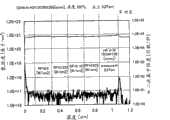
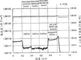
图2A是表示氩浓度的SIMS数据(与RF功率的相关性)的图示,图2B是表示氟浓度的SIMS数据(实验1)的图示;Figure 2A is a graphical representation of SIMS data representing argon concentration (as a function of RF power), and Figure 2B is a graphical representation of SIMS data representing fluorine concentration (Experiment 1);
图3A是表示氧浓度的SIMS数据的图示,图3B是表示氮浓度的SIMS数据(实验1)的图示;Figure 3A is a graphical representation of SIMS data representing oxygen concentration, and Figure 3B is a graphical representation of SIMS data representing nitrogen concentration (Experiment 1);
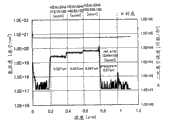
图4A是表示氩浓度的SIMS数据(与压力的相关性)的图示,图4B是表示氟浓度的SIMS数据(实验2)的图示;Figure 4A is a graphical representation of SIMS data representing argon concentration (dependence on pressure), and Figure 4B is a graphical representation of SIMS data representing fluorine concentration (Experiment 2);
图5A是表示氧浓度的SIMS数据的图示,图5B是表示氮浓度的SIMS数据(实验2)的图示;Figure 5A is a graphical representation of SIMS data representing oxygen concentration, and Figure 5B is a graphical representation of SIMS data representing nitrogen concentration (Experiment 2);
图6A至6D是说明生产有源矩阵衬底的步骤的图示;6A to 6D are diagrams illustrating steps of producing an active matrix substrate;
图7A至7C是说明有源矩阵衬底的视图;7A to 7C are views illustrating an active matrix substrate;
图8是说明有源矩阵衬底的视图;FIG. 8 is a view illustrating an active matrix substrate;
图9是说明AM-LCD外观的视图;FIG. 9 is a view illustrating the appearance of an AM-LCD;
图10是说明透射型液晶显示器件的视图;FIG. 10 is a view illustrating a transmissive liquid crystal display device;
图11A是上面的设计中的EL模块的视图,图11B是EL模块的在横截面的视图;FIG. 11A is a view of the EL module in the above design, and FIG. 11B is a view of the EL module in cross-section;
图12是EL模块的在横截面的视图;FIG. 12 is a view in cross section of an EL module;
图13A至13F是说明电子器件的视图;13A to 13F are views illustrating electronic devices;
图14A至14D是说明电子器件的视图;14A to 14D are views illustrating electronic devices;
图15A至15C是说明电子器件的视图;以及15A to 15C are views illustrating electronic devices; and
图16是用FT-IR法得到的光谱数据的图示。Fig. 16 is a graphical representation of spectral data obtained by the FT-IR method.
具体实施方式Detailed ways
(实验1)(experiment 1)
进行实验以检验通过用甲硅烷、氩和氢作为起始气体依赖于RF功率密度的等离子体CVD方法在半导体衬低上形成的非晶硅膜中的氩浓度。Experiments were conducted to examine the argon concentration in an amorphous silicon film formed on a semiconductor substrate by an RF power density-dependent plasma CVD method using monosilane, argon, and hydrogen as starting gases.
进一步,半导体衬底传送到室中,加热并保持在300℃,室内的压力用排气系统调节至66.65Pa(0.5Torr)。其次,SiH4气体从气体引入系统在100sccm的流速下引入到室中,通过等离子体CVD法形成第一非晶硅膜,同时在27.12MHz的放电频率、20W的RF功率(0.033W/cm2的RF功率密度)(600cm2的电极面积)从RF电源进行放电。第一非晶硅膜作为基准。Further, the semiconductor substrate was transferred into a chamber, heated and maintained at 300°C, and the pressure in the chamber was adjusted to 66.65 Pa (0.5 Torr) with an exhaust system. Next, SiH4 gas was introduced into the chamber from the gas introduction system at a flow rate of 100 sccm, and the first amorphous silicon film was formed by plasma CVD, while the discharge frequency was 27.12 MHz, the RF power of 20 W (0.033 W/cm2 RF power density) (electrode area of 600 cm2 ) was discharged from the RF power source. The first amorphous silicon film was used as a reference.
其次,第二非晶硅膜形成于第一非晶硅膜上,保持200nm的厚度。第二非晶硅膜通过等离子体CVD法通过保持温度在300℃、用排气系统调节室内的压力为26.66Pa(0.2Torr)、从气体引入系统向室内以100sccm的流速引入SiH4气体、500sccm的流速引入氩气、200sccm的流速引入氮气、同时在27.12MHz的放电频率、20W的RF功率(0.033W/cm2的RF功率密度)下从RF电源进行放电来形成。Next, a second amorphous silicon film was formed on the first amorphous silicon film to maintain a thickness of 200 nm. The second amorphous silicon film is maintained at 300° C. by plasma CVD, the pressure in the chamber is adjusted to 26.66 Pa (0.2 Torr) with an exhaust system, andSiH gas is introduced into the chamber at a flow rate of 100 sccm from the gas introduction system, 500 sccm Argon gas was introduced at a flow rate of 200 sccm and nitrogen gas was introduced at a flow rate of 200 sccm while discharging from an RF power supply at a discharge frequency of 27.12 MHz and an RF power of 20 W (RF power density of 0.033 W/cm2 ).
其次,只改变RF功率的条件时,在第二非晶硅膜上形成第三非晶硅膜(0.166W/cm2的RF功率密度)、第四非晶硅膜(0.333W/cm2的RF功率密度)和第五非晶硅膜(0.5W/cm2的RF功率密度)。Next, when only the RF power conditions were changed, a third amorphous silicon film (RF power density of 0.166W/cm2 ), a fourth amorphous silicon film (0.333W/cm2 RF power density) and the fifth amorphous silicon film (RF power density of 0.5 W/cm2 ).
对这样层叠在半导体衬底上的膜进行SIMS分析。测得膜中的氩浓度示于图2A中,测得膜中的氟浓度示于图2B中,测得膜中的氮浓度示于图3A中,测得膜中的氧浓度示于图3B中。从图3A中读出膜中的氮浓度为大约1×10¹⁶/cm3-大约1×1017/cm3。从图3B中读出膜中的氧浓度为大约4 X 1017/cm3-大约3 X 1018/cm3。虽然没有用图表示,膜中的碳浓度为1×1016/cm3-5 X 1017/cm3。The SIMS analysis was performed on the film thus laminated on the semiconductor substrate. The measured argon concentration in the film is shown in Figure 2A, the measured fluorine concentration in the film is shown in Figure 2B, the measured nitrogen concentration in the film is shown in Figure 3A, and the measured oxygen concentration in the film is shown in Figure 3B middle. The nitrogen concentration in the film was read from FIG. 3A to be about 1×10¹⁶ /cm3 to about 1×10¹⁷ /cm3 . The oxygen concentration in the film was read from FIG. 3B to be about 4 X 10¹⁷ /cm3 to about 3 X 10¹⁸ /cm3 . Although not shown in the graph, the carbon concentration in the film was 1×10¹⁶ /cm3 to 5×10¹⁷ /cm3 .
从图2A、2B、3A和3B中显而易见,作为使用氢、氩和甲硅烷为起始气体的结果,非晶硅膜中的氩浓度中提高到1×10²⁰/cm3-1×1021/cm3。因而,依靠使用氢、氩和甲硅烷气体作为起始气体的等离子体CVD法,形成包含高浓度,或具体地说,1×1020/cm3-1×1021/cm3的浓度的氩的非晶硅膜。另一方面,当只有甲硅烷和氩作为起始气体时,氩以约1×1018/cm3的浓度,即以大约5 X 1017/cm3-大约2 X 1018/cm3的浓度包含在膜中。As apparent from FIGS. 2A, 2B, 3A, and 3B, as a result of using hydrogen, argon, and monosilane as starting gases, the argon concentration in the amorphous silicon film increases to 1×10²⁰ /cm3 -1×10²¹ /cm3 . Thus, by virtue of the plasma CVD method using hydrogen, argon, and monosilane gas as starting gases, argon containing a high concentration, or specifically, a concentration of 1×10²⁰ /cm3 to 1×10²¹ /cm3 is formed amorphous silicon film. On the other hand, when only monosilane and argon are used as starting gases, argon is present at a concentration of about 1×10¹⁸ /cm3 , that is, at a concentration of about 5 X 10¹⁷ /cm3 to about 2 X 10¹⁸ /cm3 contained in the film.
另外,用氢、氩和甲硅烷作为起始气体,非晶硅膜中氟的浓度降到2 X 10¹⁶/cm3-8 X 1016/cm3。In addition, using hydrogen, argon and monosilane as starting gases, the concentration of fluorine in the amorphous silicon film was reduced to 2 X 10¹⁶ /cm3 -8 X 10¹⁶ /cm3 .
另外,非晶硅膜中氩的浓度随着RF功率密度的增加而增加。RF功率密度的增加几乎没有伴随膜中氟浓度、氮浓度、氧浓度或碳浓度的变化。In addition, the concentration of argon in the amorphous silicon film increases as the RF power density increases. The increase in RF power density was accompanied by little change in fluorine concentration, nitrogen concentration, oxygen concentration, or carbon concentration in the film.
(实验2)(experiment 2)
其次,依赖于改变室内压力条件时的等离子体CVD法检测非晶硅膜中氩浓度与室内压力的关系。Secondly, the relationship between the concentration of argon in the amorphous silicon film and the pressure in the chamber was detected by the plasma CVD method when the pressure condition in the chamber was changed.
首先,作为基准的第一非晶硅膜通过等离子体CVD法在与实验1相同的条件下形成于半导体衬底上。First, a reference first amorphous silicon film was formed on a semiconductor substrate by the plasma CVD method under the same conditions as in
其次,第二非晶硅膜保持200nm的厚度形成于第一非晶硅膜上。第二非晶硅膜通过等离子体CVD法通过保持温度在300℃、用排气系统调节室内的压力为5.332Pa(0.04Torr)、从气体引入系统向室内以100sccm的流速引入SiH4气体、100sccm的流速引入氩气、50sccm的流速引入氢气、同时在27.12MHz的放电频率、20W的RF功率(0.033W/cm2的RF功率密度)下从RF电源进行放电来形成。Next, a second amorphous silicon film was formed on the first amorphous silicon film maintaining a thickness of 200 nm. The second amorphous silicon film is maintained at 300°C by plasma CVD, the pressure in the chamber is adjusted to 5.332Pa (0.04Torr) with an exhaust system, SiH gas is introduced into the chamber at a flow rate of100sccm from the gas introduction system, 100sccm Argon gas is introduced at a flow rate of 50 sccm, and hydrogen gas is introduced at a flow rate of 50 sccm while discharging from an RF power source at a discharge frequency of 27.12 MHz and an RF power of 20 W (RF power density of 0.033 W/cm2 ).
其次,当改变室内压力和气体流速的条件时,在第二非晶硅膜上形成第三非晶硅膜(压力=4Pa(0.03Torr),100sccm的SiH4气体流速,50sccm的氩气流速和40sccm的氢气流速)、第四非晶硅膜(压力=2.666Pa(0.02Torr),100sccm的SiH4气体流速,15sccm的氩气流速和12sccm的氢气流速)。Next, when changing the conditions of chamber pressure and gas flow rate, a third amorphous silicon film was formed on the second amorphous silicon film (pressure = 4 Pa (0.03 Torr), SiH gas flow rate of100 sccm, argon flow rate of 50 sccm and 40 sccm hydrogen flow rate), the fourth amorphous silicon film (pressure = 2.666 Pa (0.02 Torr), 100 sccm SiH4 gas flow rate, 15 sccm argon flow rate and 12 sccm hydrogen flow rate).
对这样层叠在半导体衬底上的膜进行SIMS分析。测得膜中的氩浓度示于图4A中,测得膜中的氟浓度示于图4B中,测得膜中的氮浓度示于图5A中,测得膜中的氧浓度示于图5B中。碳浓度为1×10¹⁶/cm3-5 X 1017/cm3。The SIMS analysis was performed on the film thus laminated on the semiconductor substrate. The measured argon concentration in the film is shown in Figure 4A, the measured fluorine concentration in the film is shown in Figure 4B, the measured nitrogen concentration in the film is shown in Figure 5A, and the measured oxygen concentration in the film is shown in Figure 5B middle. The carbon concentration is 1×10¹⁶ /cm3 -5×10¹⁷ /cm3 .
从图4A、4B、5A和5B中显而易见,当压力减小,即真空度提高时,非晶硅膜中的氩浓度减小。压力的减小几乎没有伴随膜中氟浓度、氮浓度、氧浓度或碳浓度的变化。As apparent from FIGS. 4A, 4B, 5A and 5B, when the pressure decreases, that is, the degree of vacuum increases, the concentration of argon in the amorphous silicon film decreases. The decrease in pressure is accompanied by little change in fluorine concentration, nitrogen concentration, oxygen concentration or carbon concentration in the membrane.
(实验3)(Experiment 3)
下面说明的是通过等离子体CVD法用甲硅烷、氩元素和氢作为起始气体形成的非晶硅膜的质量。Described below is the quality of an amorphous silicon film formed by the plasma CVD method using monosilane, argon element and hydrogen as starting gases.
图16是表示通过Fourier变换红外线光谱法(FT-IR)从用甲硅烷、氩元素和氢作为起始气体形成的非晶硅膜中得到的光谱数据的图表。图16中,可见Si-Si键的峰在640/cm的波数,并可见另一个峰在2020/cm的波数。据报道,2000/cm的波数对应Si-H键的峰、2100/cm的波数对应Si-H2键的峰。可以说图16中在2020/cm的波数的峰主要是来自Si-H键,以及少量的Si-H2键。Fig. 16 is a graph showing spectral data obtained by Fourier transform infrared spectroscopy (FT-IR) from an amorphous silicon film formed using monosilane, argon and hydrogen as starting gases. In Fig. 16, the peak of the Si-Si bond is seen at the wave number of 640/cm, and another peak is seen at the wave number of 2020/cm. It is reported that the wave number of 2000/cm corresponds to the peak of Si-H bond, and the wave number of 2100/cm corresponds to the peak of Si-H2 bond. It can be said that the peak at the wave number of 2020/cm in Fig. 16 is mainly from Si-H bonds, and a small amount of Si-H2 bonds.
优选实施方案的说明Description of the preferred embodiment
本发明的实施方案将给予说明。Embodiments of the present invention will be described.
(实施方案1)(implementation 1)
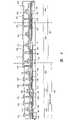
根据本发明的生产典型的TFT的过程将参考图1A至1G给予简要说明。这里说明的是使用本发明的包含稀有气体元素并具有非晶结构的半导体膜作为吸取位的实例。A process for producing a typical TFT according to the present invention will be briefly explained with reference to FIGS. 1A to 1G. Explained here is an example of using the semiconductor film of the present invention containing a rare gas element and having an amorphous structure as the gettering site.
图1A中参考编号10指具有绝缘表面的衬底,11指作为阻塞层的绝缘膜,12指具有非晶结构的半导体膜。Reference numeral 10 in FIG. 1A designates a substrate having an insulating surface, 11 designates an insulating film as a blocking layer, and 12 designates a semiconductor film having an amorphous structure.
图1A中,衬底10可以是玻璃衬底、石英衬底或陶瓷衬底。另外可以用硅衬底、金属衬底或不锈钢衬底,在其表面上形成绝缘膜。另外可以用具有热阻性能承受各步骤中的处理温度的塑料衬底。In FIG. 1A, the substrate 10 may be a glass substrate, a quartz substrate, or a ceramic substrate. Alternatively, a silicon substrate, a metal substrate or a stainless substrate may be used, and an insulating film is formed on the surface thereof. Alternatively, a plastic substrate having thermal resistance properties to withstand the processing temperature in each step can be used.
参考图1A,首先,在衬底10上形成诸如氧化硅膜、氮化硅膜或氮氧化硅膜(SiOxNy)的下层绝缘膜11。典型地,下层绝缘膜是双层结构,用SiH4、NH3和N2O作为反应气体形成第一氮氧化硅膜,保持50-100nm的厚度,在其上用SiH4和N2O作为反应气体形成第二氮氧化硅膜,保持100-150nm的厚度。另外期望下层绝缘膜11的第一层是具有不大于10nm的厚度的氮化硅膜(SiN膜)或是第二氮氧化硅膜(SiNxOy膜(x>>y))。吸取过程中,镍趋向于迁移到其中氧浓度很高的区域。因而,与半导体膜接触的下层绝缘膜是氮化硅膜是非常有意义的。另外可以通过顺序层叠第一氮氧化硅膜、第二氮氧化硅膜和氮化硅膜采用三层结构。Referring to FIG. 1A , first, an underlying insulating
其次,在下层绝缘膜上形成具有非晶结构的第一半导体膜12。第一半导体膜12由主要包括硅的半导体材料形成。典型地,非晶硅膜或非晶锗硅膜通过等离子体CVD法、减压CVD法或溅射法形成,保持10-100nm的厚度。为了通过随后的晶化得到具有良好结晶结构的半导体膜,理想的是包含在具有非晶结构的第一半导体膜12中诸如氧和氮的杂质的浓度不高于5 X 10¹⁸/cm3(用二次离子质量分析法测得的原子浓度(SIMS))。这些杂质成为阻碍随后的晶化的因素。甚至晶化之后,杂质变成增加陷阱中心和复合中心密度的原因。因而期望是使用为高真空处理而设计的CVD装置,其中反应室内部是镜面处理的(在电场下抛光)并除了使用高纯度材料气体外装配有无油抽空系统。Next, the
然后,具有非晶结构的第一半导体膜12通过日本专利公开特许号8-78329中公开的技术晶化。这项公开的技术是通过向非晶硅膜中选择性地添加金属元素以促进晶化,随后加热形成具有结晶结构的半导体膜,该半导体膜具有从金属元素添加的区域扩散开的结晶结构。首先,在具有非晶结构的第一半导体膜12的表面上,用旋转器涂敷含1-100ppm重量的金属元素(这里是镍)的醋酸镍溶液,其表现出促进晶化的催化功能从而形成含镍的层13(图1B)。除了涂敷的方法外,含镍层13还可以用诸如溅射法、蒸发法或通过等离子体处理形成极薄的膜的方法等其它方法形成。尽管涂敷是在整个表面上实施的,含镍的层可以通过形成掩膜选择性地形成。Then, the
其次,进行热处理以实现晶化。本情形中,硅化物形成在金属元素所接触的半导体膜的那部分以促进半导体的晶化,且晶化以硅化物作为核来进行。这样,形成具有结晶结构的第一半导体膜14,如图1C所示。理想的是第一半导体膜14中氧浓度在晶化以后不超过5 X 10¹⁸/cm3。这里,用于除氢的热处理(450℃,1小时)之后进行用于晶化的热处理(550-650℃,4-24小时)。当通过强光辐射进行晶化时,允许用红外线、可见光或紫外线中的任何一个或其组合。典型地,用发自卤素灯、金属卤化物灯、氙弧光灯、碳弧光灯、高压钠灯或高压汞灯的光。光源打开1-60秒,理想地,30-60秒,重复1-10次,因而半导体膜被迅速地加热到约600-约1000℃。如所需要的那样,在强光辐射之前可以进行热处理以释放具有非晶结构的第一半导体膜14中所包含的氢。另外,允许同时进行热处理和强光辐射来实现晶化。考虑到生产率,期望用强光辐射来实现晶化。Next, heat treatment is performed to achieve crystallization. In this case, silicide is formed at the portion of the semiconductor film in contact with the metal element to promote crystallization of the semiconductor, and the crystallization proceeds with the silicide as a nucleus. In this way, the first semiconductor film 14 having a crystalline structure is formed, as shown in FIG. 1C. It is desirable that the oxygen concentration in the first semiconductor film 14 does not exceed 5 X 10¹⁸ /cm3 after crystallization. Here, heat treatment for dehydrogenation (450°C, 1 hour) is followed by heat treatment for crystallization (550-650°C, 4-24 hours). When the crystallization is carried out by intense light irradiation, any one or combination of infrared rays, visible rays or ultraviolet rays is allowed. Typically, light from a halogen, metal halide, xenon arc, carbon arc, high pressure sodium or high pressure mercury lamp is used. The light source is turned on for 1-60 seconds, ideally, 30-60 seconds, and repeated 1-10 times, whereby the semiconductor film is rapidly heated to about 600-about 1000°C. As required, heat treatment may be performed to release hydrogen contained in the first semiconductor film 14 having an amorphous structure before intense light irradiation. In addition, simultaneous heat treatment and intense light irradiation are allowed to achieve crystallization. In consideration of productivity, it is desirable to achieve crystallization by intense light irradiation.
在这样所获得的第一半导体膜14中残留着金属元素(这里是镍)。金属元素残留在超过1×10¹⁹/cm3的平均浓度,尽管其可以不均匀地分布在膜中。甚至在这种状态下,允许形成TFT和各种其它半导体元件。然而,还是用后面说明的方法除去金属元素。A metal element (here, nickel) remains in the first semiconductor film 14 thus obtained. The metal element remains at an average concentration exceeding 1×10¹⁹ /cm3 , although it may be unevenly distributed in the film. Even in this state, TFTs and various other semiconductor elements are allowed to be formed. However, metal elements are also removed by the method described later.
然后,为了增加晶化的程度(晶体成分在膜总体积中的比例)并修复(fix)残留在晶粒在中的缺陷,理想的是用激光束辐射具有结晶结构的半导体膜14。当用激光束辐射时,薄的氧化物膜(没有图示)形成于表面上。作为激光束,可以用不超过400nm的波长的准分子激光束、YAG激光的二次谐波或三次谐波。还允许通过使用连续振荡激光器(YAG激光器、YVO4激光器、YLF激光器、YAlO3激光器、玻璃激光器、红宝石激光器、金绿宝石激光器或钛蓝宝石激光器)用基本波长的二次谐波到四次谐波。典型地,可以用Nd:YVO4(基本波长,1064nm)的二次谐波(532nm)或三次谐波(355nm)。当使用连续振荡激光器时,发自10W的输出的连续振荡YVO4激光器的激光束通过非线形光学元件转换成谐波。或者,可以采用通过将YVO4晶体和非线性光学元件放入谐振腔中发射谐波的方法。理想地,矩形或椭圆形的激光束通过光学系统形成于辐射的表面上,并允许落到待处理的物体上。在辐射表面上的激光束的形状(激光光斑)通过光学系统中的光束形成装置设定以采取具有3-100μm短轴直径和不小于100μm的长轴直径的椭圆形状。可以采取短边为3-100μm的长度、长边不小于100μm的矩形代替椭圆形。上面提到的形状设定为矩形或椭圆形是从衬底表面要用激光束充分退火的观点考虑的。这里,长轴(长边)的长度设为不小于100μm是从以下观点考虑的,即当激光束具有适于激光退火的能量密度时,那么操作者可以适当地决定长轴(或长边)的长度。本情形中,能量密度必须是大约0.01-大约100MW/cm2(优选地0.1-10MW/cm2)。半导体膜可以相对于激光束在大约10-大约2000cm/s的速度移动,以便于用激光束辐射。Then, in order to increase the degree of crystallization (the ratio of crystal components in the total volume of the film) and to fix defects remaining in crystal grains, it is desirable to irradiate the semiconductor film 14 having a crystal structure with a laser beam. When irradiated with a laser beam, a thin oxide film (not shown) is formed on the surface. As the laser beam, an excimer laser beam having a wavelength not exceeding 400 nm, a second harmonic wave or a third harmonic wave of YAG laser light can be used. It also allows the use of continuous oscillation lasers (YAG lasers, YVO4 lasers, YLF lasers, YAlO3 lasers, glass lasers, ruby lasers, chrysoberyl lasers, or titanium sapphire lasers) from the second harmonic to the fourth harmonic of the fundamental wavelength . Typically, the second harmonic (532nm) or third harmonic (355nm) of Nd:YVO4 (fundamental wavelength, 1064nm) can be used. When a continuous oscillation laser is used, a laser beam from a continuous oscillation YVO4 laser of output of 10 W is converted into harmonics by a nonlinear optical element. Alternatively, a method of emitting harmonics by placing a YVO4 crystal and a nonlinear optical element in a resonant cavity can be used. Ideally, a rectangular or elliptical laser beam is formed by the optical system on the surface of the radiation and allowed to fall on the object to be treated. The shape of the laser beam (laser spot) on the radiation surface is set by the beam forming means in the optical system to take an elliptical shape having a minor axis diameter of 3-100 μm and a major axis diameter of not less than 100 μm. Instead of an ellipse, a rectangle having a short side of 3-100 μm in length and a long side of not less than 100 μm may be adopted. The above-mentioned setting of the shape as a rectangle or an ellipse is considered from the viewpoint that the substrate surface is sufficiently annealed with a laser beam. Here, the length of the long axis (long side) is set to be not less than 100 μm from the viewpoint that when the laser beam has an energy density suitable for laser annealing, then the operator can appropriately determine the long axis (or long side) length. In this case, the energy density must be about 0.01 to about 100 MW/cm2 (preferably 0.1 to 10 MW/cm2 ). The semiconductor film may be moved at a speed of about 10 to about 2000 cm/s relative to the laser beam so as to be irradiated with the laser beam.
通过用激光束辐射形成的氧化物膜在晶化后是不充分的。因而,通过使用含臭氧的水溶液(典型地臭氧水)形成氧化物膜(称为化学氧化)从而形成具有1-10nm的总厚度的氧化物膜的阻挡层15,且含稀有气体元素的第二半导体膜16形成于阻挡层15上(图1D)。这里,通过用激光束辐射具有结晶结构的第一半导体膜14形成的氧化物膜也被认为是阻挡层的一部分。当第二半导体膜16在后续步骤中仅仅被选择性地除去时,阻挡层15是作为刻蚀阻止层工作的。化学氧化物能简单地甚至通过用其中硫酸、盐酸、硝酸和过氧化氢混合在一起的水溶液代替使用含臭氧的水溶液处理来形成。阻挡层15可以另外通过用紫外线在氧化气氛中辐射产生臭氧来氧化具有结晶结构的半导体膜的表面形成。阻挡层15另外可以通过等离子体CVD法、溅射法或蒸发法淀积保持约1-10nm的厚度的氧化物膜来形成。当阻挡层通过等离子体CVD法、溅射法或蒸发法形成时,理想的是阻挡层在冲洗具有结晶结构的半导体膜表面并且除去自发氧化的膜或用激光辐射形成的氧化物膜之后形成。An oxide film formed by irradiation with a laser beam is insufficient after crystallization. Thus, the
当等离子体CVD法用于阻挡层的形成时,用硅烷气体(甲硅烷、乙硅烷或丙硅烷)和氮氧气体(能用NOx表示的气体)作为起始气体,用脉冲振荡形成膜。也就是,氮氧化硅膜通过用甲硅烷(SiH4)和氧化氮(N2O)或TEOS气体和N2O或TEOS气体、N2O和O2作为起始气体形成不大于10nm,优选地,不大于5nm的厚度。与通过用含臭氧的水溶液(典型地,臭氧水)得到的氧化物膜(称为化学氧化物)和通过用紫外线在氧化气氛中辐射产生臭氧来氧化具有结晶结构的半导体膜的表面形成的氧化物膜相比,氮氧化硅膜非常紧密地附着在具有结晶结构的第一半导体膜上且在随后的形成(第二半导体膜的)步骤中不发生剥落。为了进一步改善紧密附着性,用氩等离子体的处理可以在形成阻挡层之前实现。另外,在吸取的步骤中,具有处于上述范围内的厚度的氮氧化硅膜允许金属元素穿过阻挡层以便于迁移到吸取位中。When the plasma CVD method is used for the formation of the barrier layer, a film is formed by pulse oscillation using silane gas (monosilane, disilane or trisilane) and nitrogen oxygen gas (gas that can be represented by NOx ) as starting gases. That is, the silicon oxynitride film is formed not larger than 10 nm by using monosilane (SiH4 ) and nitrogen oxide (N2 O) or TEOS gas and N2 O or TEOS gas, N2 O and O2 as starting gases, preferably ground, with a thickness not greater than 5nm. Oxidation formed by oxidizing the surface of a semiconductor film having a crystalline structure by oxidizing an oxide film (called a chemical oxide) obtained by using an aqueous solution containing ozone (typically, ozone water) and generating ozone by irradiating ultraviolet rays in an oxidizing atmosphere The silicon oxynitride film adheres very closely to the first semiconductor film having a crystalline structure and does not peel off in the subsequent step of forming (of the second semiconductor film) compared to a physical film. In order to further improve tight adhesion, treatment with argon plasma can be carried out before forming the barrier layer. In addition, in the step of gettering, the silicon oxynitride film having a thickness within the above range allows the metal element to pass through the barrier layer to facilitate migration into the gettering site.
另外,当等离子体CVD法用于形成阻挡层时,含稀有气体元素的第二半导体膜和阻挡层能够在不与外界空气接触时形成。此外,它们可以在同样的室里连续形成,以保持高的生产量。In addition, when the plasma CVD method is used to form the barrier layer, the second semiconductor film containing a rare gas element and the barrier layer can be formed without contact with the outside air. Furthermore, they can be formed consecutively in the same chamber to maintain high throughput.
另外阻挡层15能通过在大约200-350℃加热洁净炉形成薄的氧化物膜来形成。通过上述方法中任何一种或通过这些方法的组合形成的阻挡层15必须拥有允许第一半导体膜中的镍在后续的吸取中迁移到第二半导体膜中的膜质量或膜厚度。本技术说明中,阻挡层是具有允许金属元素在吸取的步骤中穿透、并在除去变成吸取位的层的步骤中作为刻蚀阻止层的一层。Alternatively the
这里,用等离子体CVD法形成含稀有气体元素的第二半导体膜16,以形成吸取位。作为稀有气体元素,能够用选自氦(He)、氖(Ne)、氩(Ar)、氪(Kr)和氙(Xe)中的一个或多个。其中,理想的是用氩(Ar),它是廉价的可用气体。这里,通过等离子体CVD法,用甲硅烷、氩和氢作为起始气体形成含1×10¹⁸/cm3-1×1022/cm3,优选地1×1020/cm3-1×1021/cm3浓度的氩的第二半导体膜以得到吸取效果。第二半导体膜中,氟浓度降低到2 X 1016/cm3-8 X 1016/cm3,氢浓度也采用相对小的值。Here, the
因为两个原因,形成惰性气体的稀有气体元素被包含在膜中。一个原因是形成悬挂键以给予半导体膜畸变。另一个原因是将畸变给予半导体膜的晶格中。当使用诸如氩(Ar)氪(Kr)或氙(Xe)这样具有大于硅的原子半径的元素时,畸变给予半导体膜的晶格中,达到显著的程度。另外,用包含在膜中的稀有气体元素,不仅晶格发生畸变,而且形成有利于得到吸取作用的非对称键。Noble gas elements forming noble gases are contained in the film for two reasons. One reason is the formation of dangling bonds to impart distortion to the semiconductor film. Another reason is imparting distortion in the crystal lattice of the semiconductor film. When an element having an atomic radius larger than silicon such as argon (Ar) krypton (Kr) or xenon (Xe) is used, distortion is imparted to the crystal lattice of the semiconductor film to a significant degree. In addition, with the rare gas element contained in the film, not only the crystal lattice is distorted, but also an asymmetric bond is formed which is favorable for obtaining the absorption effect.
其次,实现热处理以进行用于减少第一半导体元件所包含的金属元素(镍)的浓度或用于除去该金属元素的吸取(图1E)。吸取通过用强光辐射或通过热处理来进行。由于吸取,金属元素沿着图1E中箭头的方向迁移(即,沿着从衬底侧到第二半导体膜表面的方向),包含在被阻挡层15覆盖的第一半导体层14中的金属元素被除去,或其中金属元素的浓度减少。金属元素在吸取过程中迁移的距离需要至少粗略的为第一半导体膜的厚度,并且吸取在相对短的时间周期内完成。这里,镍全部迁移到第二半导体膜16中,所以不会分离在第一半导体膜14中;即在第一半导体膜中14中几乎不包含镍。也就是,吸取进行到充分的程度以便于膜中的镍浓度变得不大于1×10¹⁸/cm3,或理想地,不大于1×1017/cm3。Next, heat treatment is performed to perform gettering for reducing the concentration of the metal element (nickel) contained in the first semiconductor element or for removing the metal element (FIG. 1E). Absorption takes place by irradiation with intense light or by heat treatment. Due to the absorption, the metal element migrates in the direction of the arrow in FIG. be removed, or the concentration of metal elements in it is reduced. The distance that the metal element migrates during gettering needs to be at least roughly the thickness of the first semiconductor film, and gettering is completed within a relatively short period of time. Here, nickel completely migrates into the
依赖于用于吸取的热处理的条件或第二半导体膜的厚度,第二半导体膜经常部分地晶化。当第二半导体膜晶化时,导致了悬挂键、晶格畸变和非对称键的减少,吸取效果降低。因而,理想地,热处理条件和第二半导体膜的厚度是使第二半导体膜不被晶化的条件和厚度。无论如何,第二半导体膜,即含稀有气体元素的非晶硅膜,比不含稀有气体元素的非晶硅膜更不容易晶化,并最适合于作为吸取位。Depending on the conditions of the heat treatment for gettering or the thickness of the second semiconductor film, the second semiconductor film is often partially crystallized. When the second semiconductor film is crystallized, dangling bonds, lattice distortion, and asymmetric bonds are reduced, and the sucking effect is reduced. Thus, ideally, the heat treatment conditions and the thickness of the second semiconductor film are conditions and thicknesses such that the second semiconductor film is not crystallized. In any case, the second semiconductor film, that is, an amorphous silicon film containing a rare gas element, is less likely to be crystallized than an amorphous silicon film not containing a rare gas element, and is most suitable as a gettering site.
依赖于吸取的热处理条件,第一半导体膜的晶化程度能随着吸取同时得到增强,以修复留在晶粒中的缺陷,即,改善结晶性能。Depending on the heat treatment conditions for the uptake, the degree of crystallization of the first semiconductor film can be enhanced simultaneously with the uptake to repair defects remaining in crystal grains, ie, to improve crystallization properties.
本技术说明中,吸取代表待吸取的区域中(这里是第一半导体膜)的金属元素由于热能被释放并由于扩散而迁移到吸取位。因而,吸取依赖于处理温度并由于温度升高在短的时间周期内进行。In this specification, gettering means that a metal element in a region to be gettered (here, the first semiconductor film) is released due to thermal energy and migrates to a gettering site due to diffusion. Thus, uptake is process temperature dependent and takes place within a short period of time due to temperature rise.
在通过用强光辐射处理的情形中,用于加热的光源打开1-60秒,优选地,30-60秒,重复1-10次,优选地2-6次。虽然光源的光强度可以任意地选择,但是被这样选择以便于半导体膜迅速地加热到600-1000℃,优选地大约700-大约750℃。In the case of treatment by irradiation with strong light, the light source for heating is turned on for 1-60 seconds, preferably, 30-60 seconds, and repeated 1-10 times, preferably 2-6 times. Although the light intensity of the light source can be selected arbitrarily, it is selected so that the semiconductor film is rapidly heated to 600-1000°C, preferably about 700-about 750°C.
热处理的情形中,热处理在氮气氛中在450-800℃进行1-24小时,例如,在550℃进行14小时。可以辐射强光代替热处理。In the case of heat treatment, the heat treatment is performed in a nitrogen atmosphere at 450-800°C for 1-24 hours, for example, at 550°C for 14 hours. Intense light can be radiated instead of heat treatment.
其次,用阻挡层15作为刻蚀阻止层,指定为16的第二半导体膜只被选择性地除去。之后,除去阻挡层15,依靠众所周知图形形成技术对第一半导体膜14形成图形以形成所需形状的半导体层17(图1F)。作为只选择性地刻蚀第二半导体膜的方法,可采用无需等离子体的基于ClF3的干刻或用诸如包含联氨或氢氧化四乙铵(化学式(CH3)4NOH)的水溶液的碱溶液湿刻。即使除去第二半导体膜之后,用TXRF测量阻挡层表面内的镍浓度,仍旧很高。因而用期望用含氢氟酸的刻蚀剂除去阻挡层。阻挡层除去以后,进一步,期望在形成由抗蚀剂构成的掩膜之前用臭氧水形成薄的氧化物膜。Next, using the
其次,半导体层的表面用含氢氟酸刻蚀剂清洗,形成主要包括硅的绝缘膜以形成栅绝缘膜18。理想的是表面的清洗和栅绝缘膜的形成在不暴露于外界空气时连续地进行。Next, the surface of the semiconductor layer is cleaned with an etchant containing hydrofluoric acid, and an insulating film mainly composed of silicon is formed to form the
栅绝缘膜的表面清洗之后,形成栅电极19。然后,添加杂质元素(P、As等)或在该情形中添加磷以给予半导体n型从而形成源区20和漏区21。添加了杂质元素以后,进行热处理,辐射强光或辐射激光以激活杂质元素。另外,激活的同时,恢复由等离子体对栅绝缘膜的损害或恢复由等离子体对栅绝缘膜和半导体层之间的界面的损害。特别是,如果杂质元素在室温的气氛下用YAG激光器的二次谐波从前面或从背面辐射到300℃来激活的话,特别有效。YAG激光器因其需要较少的维护,所以是优选的激活装置。After the surface of the gate insulating film is cleaned, the
在随后的步骤中,形成夹层绝缘膜23,氢化之后形成到达源区和漏区的接触孔,并形成源电极24和漏电极25以完成TFT(n沟道TFT)(图1G)。In subsequent steps, interlayer insulating film 23 is formed, contact holes reaching source and drain regions are formed after hydrogenation, and
这样得到的TFT的沟道形成区22包含浓度小于1×10¹⁷/cm3的金属元素。The
本发明不局限于图1G的TFT结构,只有根据需要可采取在沟道形成区和漏区(或源区)之间具有LDD区的低密度漏(LDD:轻掺杂漏)结构。这个结构中,在沟道形成区和以高浓度添加杂质元素形成的源区或漏区之间提供以低浓度添加杂质元素的区域。该区域称作LDD区。另外还可以采用所谓的GOLD(源漏重叠LDD)结构,其中LDD区通过栅绝缘膜重叠在栅电极上。The present invention is not limited to the TFT structure of FIG. 1G, but only a low-density drain (LDD: lightly doped drain) structure having an LDD region between the channel formation region and the drain region (or source region) can be adopted as required. In this structure, a region where an impurity element is added at a low concentration is provided between a channel formation region and a source region or a drain region where an impurity element is added at a high concentration. This area is called the LDD area. Alternatively, a so-called GOLD (Source-Drain Overlapped LDD) structure in which an LDD region overlaps a gate electrode via a gate insulating film may also be employed.
尽管这里的说明涉及n沟道TFT,无需指出p沟道TFT也能通过以p型杂质元素代替n型杂质元素来形成。Although the description here refers to n-channel TFTs, it need not be pointed out that p-channel TFTs can also be formed by substituting p-type impurity elements for n-type impurity elements.
另外,虽然,这里的说明涉及顶栅型TFT,本发明能应用于无论何种TFT结构。例如,本发明能应用于底栅型(反转交错的)TFT和向前交错型(forwardly staggered)TFT。In addition, although the description herein refers to a top gate type TFT, the present invention can be applied to any TFT structure. For example, the present invention can be applied to bottom gate type (inverted staggered) TFTs and forwardly staggered type (forwardly staggered) TFTs.
(实施方案2)(implementation 2)
本实施方案中,本发明的含稀有气体元素并具有非晶结构的半导体膜被用作TFT的有源层。In this embodiment, the semiconductor film of the present invention containing a rare gas element and having an amorphous structure is used as an active layer of a TFT.
首先,栅电极形成于具有绝缘表面的衬底上,形成栅绝缘膜以覆盖栅电极,本发明的含稀有气体元素的并具有非晶结构的第一半导体膜形成于栅绝缘膜上。这里用的起始气体是甲硅烷、氩和氢,由此通过等离子体CVD形成具有非晶结构的第一半导体膜,以包含1×10¹⁸/cm3-1×1022/cm3,优选地,1×1020/cm3-1×1021/cm3的氩浓度、2 X 1016/cm3-8 X 1016/cm3的氟浓度和相对低的浓度的氢。然后,含一种导电类型(n型或p型)的杂质元素的第二半导体膜层叠在其上。然后,具有非晶结构的第一半导体膜的除了变成有源层的部分以外的不必要的部分通过刻蚀除去。然后,导电膜形成于整个表面上,导电膜和含一种导电类型(n-型或p型)的杂质元素的第二半导体膜的部分被除去,从而形成半导体膜的源区和漏区,同时,形成导电膜的漏线路和源线路。另外,部分除去第一半导体膜以制备沟道刻蚀的底栅型结构的TFT。配备了像素电极后,TFT能用于液晶显示器件的像素部分。First, a gate electrode is formed on a substrate having an insulating surface, a gate insulating film is formed to cover the gate electrode, and the first semiconductor film of the present invention containing a rare gas element and having an amorphous structure is formed on the gate insulating film. The starting gases used here are monosilane, argon and hydrogen, whereby the first semiconductor film having an amorphous structure is formed by plasma CVD to contain 1×10¹⁸ /cm3 -1×10²² /cm3 , preferably Basically, an argon concentration of 1×10²⁰ /cm3 to 1×10²¹ /cm3 , a fluorine concentration of 2×10¹⁶ /cm3 to 8×10¹⁶ /cm3 , and a relatively low concentration of hydrogen. Then, a second semiconductor film containing an impurity element of one conductivity type (n-type or p-type) is laminated thereon. Then, unnecessary portions of the first semiconductor film having an amorphous structure other than the portion that becomes the active layer are removed by etching. Then, a conductive film is formed on the entire surface, the conductive film and a portion of the second semiconductor film containing an impurity element of one conductivity type (n-type or p-type) are removed, thereby forming a source region and a drain region of the semiconductor film, At the same time, a drain line and a source line of the conductive film are formed. In addition, the first semiconductor film is partially removed to prepare a channel-etched bottom-gate type TFT. Equipped with pixel electrodes, TFTs can be used in the pixel portion of liquid crystal display devices.
另外,不局限于上述所谓非晶TFT的TFT,本发明另外能用于所谓多晶TFT的TFT的有源层。In addition, the present invention is not limited to the TFT of the above-mentioned so-called amorphous TFT, and the present invention can also be applied to the active layer of the TFT of the so-called polycrystalline TFT.
本情形中,本发明的含稀有气体元素并具有非晶结构的第一半导体膜被用作具有非晶结构的第一半导体膜12,其形成于实施方案1中所示的下层绝缘膜上。具有结晶结构的半导体通过基于晶化技术(固相生长法、激光晶化法或基于用金属元素作为催化剂的热处理法)实现晶化,并被形成图形以便于用它作为TFT的有源层。因为含有降低的浓度的氢和氟,本发明的具有非晶结构的半导体膜有利地被晶化。这里用的起始气体是甲硅烷、氩和氢,由此通过等离子体CVD形成具有非晶结构的第一半导体膜,包含1×10¹⁸/cm3-1×1022/cm3,优选地1×1020/cm3-1×1021/cm3浓度的氩。In this case, the first semiconductor film containing a rare gas element and having an amorphous structure of the present invention is used as the
当晶化通过用,例如,激光实现时,含稀有气体元素和氮并具有结晶结构的第一半导体膜形成于具有绝缘表面的衬底上,随后用激光晶化。When crystallization is performed by using, for example, a laser, a first semiconductor film containing a rare gas element and nitrogen and having a crystalline structure is formed on a substrate having an insulating surface, followed by crystallization with a laser.
所用的激光束可以是脉冲振荡型或连续发光准分子激光器、YAG激光器、YVO4激光器、YLF激光器、YAlO3激光器、玻璃激光器、红宝石激光器、金绿宝石激光器或钛蓝宝石激光器的激光束。当使用这些激光器时,发自激光振荡器的激光束通过光学系统被线性地聚集并投影到半导体膜上。晶化的条件由操作者适当地选择。当使用脉冲振荡型准分子激光器时,脉冲振荡频率选为30Hz,激光能量密度选为100-400mJ/cm2(典型地200-300mJ/cm2)。另外,当使用脉冲振荡型YAG激光器或YVO4激光器时,使用二次谐波或三次谐波,脉冲振荡频率选为1-10kHz,激光能量密度选为300-600mJ/cm2(典型地,350-500mJ/cm2)。线性聚焦以具有100-1000μm宽度的激光束,例如400μm,投到衬底的整个上,线形光束以80-98%的比例(重叠比)重叠。The laser beam used may be a laser beam of a pulse oscillation type or a continuous emitting excimer laser, a YAG laser, aYVO4 laser, a YLF laser, aYAlO3 laser, a glass laser, a ruby laser, a chrysoberyl laser or a titanium sapphire laser. When these lasers are used, a laser beam from a laser oscillator is linearly collected and projected onto a semiconductor film by an optical system. Conditions for crystallization are appropriately selected by an operator. When a pulse oscillation type excimer laser is used, the pulse oscillation frequency is selected to be 30 Hz, and the laser energy density is selected to be 100-400 mJ/cm2 (typically 200-300 mJ/cm2 ). In addition, when a pulse oscillation type YAG laser or YVO4 laser is used, the second harmonic or the third harmonic is used, the pulse oscillation frequency is selected to be 1-10 kHz, and the laser energy density is selected to be 300-600 mJ/cm2 (typically, 350 -500mJ/cm2 ). A laser beam focused linearly to have a width of 100-1000 μm, for example 400 μm, is projected onto the entire substrate, and the linear beams overlap at a ratio (overlap ratio) of 80-98%.
当使用以YVO4激光器为代表的连续振荡型激光器时,发自10W输出的连续振荡型YVO4激光器的激光束通过非线性光学元件转换成谐波(二次谐波-四次谐波)。可以采用通过将YVO4晶体和非线性光学元件放入谐振腔中来发射谐波。优选地,激光束在辐射面上通过光学系统形成为矩形或椭圆形,并投到待处理的物体上。这里,能量密度必须是大约0.01-大约100MW/cm2(优选地0.1-10MW/cm2)。当以0.5-2000cm/sec的速度相对于激光束运动同时,半导体膜可以用激光束辐射。When a continuous oscillation type laser represented by a YVO4 laser is used, a laser beam from a continuous oscillation type YVO4 laser of 10 W output is converted into harmonics (second harmonic - fourth harmonic) by a nonlinear optical element. Harmonics can be emitted by placing a YVO4 crystal and a nonlinear optical element in a resonant cavity. Preferably, the laser beam is formed into a rectangle or ellipse by an optical system on the radiating surface, and projected onto the object to be processed. Here, the energy density must be about 0.01 to about 100 MW/cm2 (preferably 0.1 to 10 MW/cm2 ). The semiconductor film may be irradiated with the laser beam while moving at a speed of 0.5 to 2000 cm/sec relative to the laser beam.
(实施方案3)(Embodiment 3)
本发明的含稀有气体元素并具有非晶结构的半导体膜可用作一种层(剥落层),其由于刻蚀或在元件已经形成于衬底上之后将诸如TFT的元件从衬底上分离时用激光束的辐射,在界面上或层内发生剥落。剥落层形成于与之接触的衬底上,并在剥落层上形成绝缘膜和TFT。The semiconductor film containing a rare gas element and having an amorphous structure of the present invention can be used as a layer (exfoliation layer) that separates an element such as a TFT from a substrate due to etching or after the element has been formed on the substrate. When irradiated with a laser beam, exfoliation occurs on the interface or within the layer. A peeling layer is formed on the substrate in contact therewith, and an insulating film and TFTs are formed on the peeling layer.
与具有非晶结构的传统半导体相比,本发明的含稀有气体元素并具有非晶结构的半导体膜以不同的速率刻蚀并能在各种刻蚀步骤中用作刻蚀阻止层。Compared with conventional semiconductors having an amorphous structure, the semiconductor film containing a rare gas element and having an amorphous structure of the present invention is etched at a different rate and can be used as an etch stopper in various etching steps.
另外,本发明的包括稀有气体元素的非晶半导体膜能用作通过不同于实施方案1所说明的方法晶化的半导体膜和其它普通半导体膜的吸取位。In addition, the amorphous semiconductor film including a rare gas element of the present invention can be used as a gettering site of a semiconductor film crystallized by a method different from that explained in
如上所述构成的本发明将以工作实例的方式进一步详细说明。The present invention constituted as above will be further explained in detail by way of working examples.
实例example
(实例1)(Example 1)
本发明的一个实例参考图6A至8说明。这里,详细说明在同一衬底上同时制造像素部分和配备在像素部分外围的驱动电路的TFT(n沟道TFT和p沟道TFT)。An example of the present invention is described with reference to FIGS. 6A to 8 . Here, TFTs (n-channel TFTs and p-channel TFTs) that simultaneously manufacture a pixel portion and a driver circuit provided on the periphery of the pixel portion on the same substrate will be described in detail.
首先,基础绝缘膜形成于衬底100上,得到具有结晶结构的第一半导体膜。然后,半导体膜被刻蚀以具有所需的形状以形成以岛状互相分离的半导体层102-106。First, a base insulating film is formed on a
玻璃衬底(#1737)用作衬底100。对于基础绝缘膜101,以SiH4、NH3和N2O为材料气体(组分比:Si=32%,O=27%,N=24%,H=17%)形成的氮氧化硅膜101a通过等离子体CVD在400℃的膜淀积温度温度下形成50nm(优选地10-200nm)的厚度。然后,用臭氧水清洁表面以后,表面上的氧化物膜通过稀释的氢氟酸(1/100稀释)除去。其次,以SiH4和N2O为材料气体(组分比:Si=32%,O=59%,N=7%,H=2%)形成的氮氧氢化硅膜(silicon hydride oxynitride film)101b通过等离子体CVD在400℃的膜淀积温度温度下在其上形成100nm(优选地50-200nm)的厚度以从而形成叠层。另外,不暴露于大气中,通过等离子体CVD在300℃的膜淀积温度下以SiH4为膜淀积气体形成具有非晶结构的半导体膜(该情形中是非晶硅膜),具有54nm(优选地25-80nm)的厚度。A glass substrate (#1737) was used as the
本实例中,基础膜101以两层结构的形式给出,但是可以采用绝缘膜的单层或其中其两层或多层层叠的结构。另外,对半导体膜的材料没有限制。然而,半导体膜优选地优硅或锗硅(SixGe1-x(x=0.0001-0.02))合金通过已知方法(溅射、LPCVD、等离子体CVD等)形成。另外,等离子体CVD装置可以是单片型或批量型。此外,基础绝缘膜和半导体膜可以在不暴露于大气中的条件下在相同的膜淀积室中连续地形成。In this example, the
接下来,具有非晶结构的半导体膜表面被清洁之后,由臭氧水在表面形成约2nm厚度的极薄的氧化物膜。然后,为了控制TFT的阈值,实施少量杂质元素(硼或磷)的掺杂。使用离子掺杂法,其中硼烷(B2H6)在没有质量分离时被等离子体激发,硼在15kV的加速电压、30sccm的用氢稀释到1%的硼烷的气流速率、2 X 10¹²/cm2的剂量的掺杂条件下添加到非晶硅膜中。Next, after the surface of the semiconductor film having an amorphous structure is cleaned, an extremely thin oxide film with a thickness of about 2 nm is formed on the surface by ozone water. Then, in order to control the threshold of the TFT, doping of a small amount of impurity element (boron or phosphorus) is performed. Using ion doping method, wherein borane (B2 H6 ) is excited by plasma without mass separation, boron at an accelerating voltage of 15 kV, a gas flow rate of 30 sccm of borane diluted to 1% with hydrogen, 2 X 10 Added to the amorphous silicon film under the doping condition of the dose of12 /cm2 .
然后,用旋转器涂敷含100ppm重量的镍的醋酸镍盐溶液。还可以用通过旋转器将镍元素喷射到整个表面上的方法代替涂敷。Then, a nickel acetate salt solution containing 100 ppm by weight of nickel was applied using a spinner. Instead of coating, it is also possible to spray the nickel element over the entire surface by means of a spinner.
然后,进行热处理以实施晶化,从而形成具有结晶结构的半导体膜。可以进行使用电炉的加热工艺或强光的辐射用于这热处理。在使用电炉的加热工艺的情形中,可以在500-650℃进行4-24小时。这里,进行用于除氢的加热工艺(500℃,1小时)之后,进行用于晶化的加热工艺(550℃,4小时),从而得到具有结晶结构的硅膜。注意,虽然通过使用电炉的加热工艺实施晶化,还可以通过灯退火装置实施晶化。而且,注意,虽然这里用使用镍作为促进硅晶化的金属元素的晶化技术,还可以用其它已知的晶化技术,例如,固相生长法和激光晶化法。Then, heat treatment is performed to effect crystallization, thereby forming a semiconductor film having a crystalline structure. A heating process using an electric furnace or radiation of strong light may be performed for this heat treatment. In the case of the heating process using an electric furnace, it may be performed at 500-650° C. for 4-24 hours. Here, after performing a heating process for hydrogen removal (500° C., 1 hour), a heating process for crystallization (550° C., 4 hours) is performed, thereby obtaining a silicon film having a crystalline structure. Note that although crystallization is performed by a heating process using an electric furnace, crystallization can also be performed by a lamp annealing device. Also, note that although a crystallization technique using nickel as a metal element for promoting crystallization of silicon is used here, other known crystallization techniques such as solid phase growth method and laser crystallization method may also be used.
其次,用稀释的氢氟酸等除去具有结晶结构的硅膜表面上的氧化物膜之后,在大气中或氧气氛中实施第一激光辐射(XeCl:308nm的波长)用于提高晶化速率并修复残留在晶粒中的缺陷。具有400nm或更短波长的准分子激光,或YAG激光的二次谐波或三次谐波被用于激光。任何情形中,使用具有大约10-1000Hz的重复频率的脉冲激光,脉冲激光通过光学系统会聚成100-500mJ/cm2,用90-95%的重叠比实施辐射,由此可以扫描硅膜。这里,第一激光的辐射用30Hz的重复频率和393mJ/cm2的能量密度在大气中实施。注意,由于辐射在大气中或在氧气氛中进行,通过第一激光辐射在表面上形成氧化物膜。Next, after removing the oxide film on the surface of the silicon film having a crystalline structure with diluted hydrofluoric acid or the like, the first laser irradiation (XeCl: wavelength of 308 nm) is performed in the air or in an oxygen atmosphere for increasing the crystallization rate and Repair defects remaining in the die. An excimer laser having a wavelength of 400 nm or less, or a second or third harmonic of YAG laser is used for the laser. In any case, the silicon film can be scanned using pulsed laser light having a repetition frequency of about 10-1000 Hz, which is condensed to 100-500 mJ/cm2 by an optical system, and irradiated with an overlap ratio of 90-95%. Here, irradiation of the first laser light was carried out in the atmosphere with a repetition rate of 30 Hz and an energy density of 393 mJ/cm2 . Note that since the irradiation is performed in the air or in an oxygen atmosphere, an oxide film is formed on the surface by the first laser irradiation.
其次,通过第一光辐射形成的氧化物膜被稀释的氢氟酸除去之后,在氮气氛或真空中实施第二激光辐射,从而平整半导体膜表面。具有400nm或更短波长的准分子激光,或YAG激光的二次谐波或三次谐波被用于激光(第二激光)。让第二激光的能量密度高于第一激光的,优选地高30-60mJ/cm2。这里,第二激光的辐射用30Hz的重复频率和453mJ/cm2的能量密度实施,从而将半导体膜表面内不均匀性的P-V值设定为5nm或更少。第二激光辐射的情形中,由第一激光辐射形成的不均匀性(P-V值:峰对谷,高度最大值和最小值之间的差别)等级的差别减小了,即,平坦化了。这里,不均匀性的P-V值可以用AFM(原子力显微镜)观察。Next, after the oxide film formed by the first light irradiation is removed by diluted hydrofluoric acid, second laser irradiation is performed in a nitrogen atmosphere or in a vacuum, thereby flattening the surface of the semiconductor film. Excimer laser light having a wavelength of 400 nm or shorter, or the second or third harmonic wave of YAG laser light is used for the laser light (second laser light). Let the energy density of the second laser be higher than that of the first laser, preferably 30-60 mJ/cm2 . Here, the irradiation of the second laser light was performed with a repetition frequency of 30 Hz and an energy density of 453 mJ/cm2 , thereby setting the PV value of unevenness within the surface of the semiconductor film to 5 nm or less. In the case of the second laser radiation, the difference in level of non-uniformity (PV value: peak-to-valley, difference between height maximum value and minimum value) formed by the first laser radiation is reduced, that is, flattened. Here, the PV value of the inhomogeneity can be observed with an AFM (atomic force microscope).
另外,虽然本实例中在表面上进行第二激光辐射,由于关电流的减小特别对像素部分的TFT有影响,可以采用至少在像素部分选择性地实施辐射的步骤。In addition, although the second laser irradiation is performed on the surface in this example, since the reduction of off current affects especially the TFT of the pixel portion, a step of selectively performing irradiation at least at the pixel portion may be employed.
本实例中,说明用第二激光辐射平面化的实例,然而不需要特别地实施。In this example, an example of planarization with second laser radiation is described, however, it does not need to be particularly implemented.
其次,用臭氧水处理表面120秒,从而形成包括1-5nm总厚度的氧化物膜的阻挡层。Next, the surface was treated with ozone water for 120 seconds, thereby forming a barrier layer including an oxide film with a total thickness of 1-5 nm.
然后,包括氩元素的非晶硅膜,其将通过实施方案1所示的等离子体CVD成为吸取位,以150nm的厚度形成于阻挡层上。Then, an amorphous silicon film including an argon element, which will become a gettering site by plasma CVD shown in
本实例中用等离子体CVD的膜淀积条件是:26.66Pa(0.2Torr)的膜淀积压力;100sccm的气(SiH4)流速率;500sccm的气(Ar)流速率,从装置系统中引入。并且,用27.12MHz的放电、300W的RF充电(RF功率密度0.5W/cm2)实施放电。注意,在上述条件下,非晶硅膜中包含的氩元素的原子浓度是1×1020/cm3-1×1021/cm3。之后,用灯退火装置在650℃进行3分钟的热处理以实施吸取。The film deposition conditions with plasma CVD in this example are: film deposition pressure of 26.66Pa (0.2Torr); gas (SiH4 ) flow rate of 100 sccm; gas (Ar) flow rate of 500 sccm, introduced from the device system . Then, discharge was performed by 27.12 MHz discharge and 300 W RF charge (RF power density 0.5 W/cm2 ). Note that under the above conditions, the atomic concentration of the argon element contained in the amorphous silicon film is 1×10²⁰ /cm3 to 1×10²¹ /cm3 . Thereafter, heat treatment was performed at 650° C. for 3 minutes using a lamp annealing apparatus to perform absorption.
接下来,含氩元素的非晶硅膜,其是吸取位,用阻挡层作为刻蚀阻止层被选择性地除去,然后,用稀释的氢氟酸选择性地除去阻挡层。注意,有一个趋势,即镍在吸取过程中容易移动到具有高氧浓度的区域,这样,理想的是包括氧化物膜的阻挡层在吸取之后被除去。Next, the amorphous silicon film containing argon element, which is the gettering site, is selectively removed using the stopper layer as an etching stopper, and then, the stopper layer is selectively removed with diluted hydrofluoric acid. Note that there is a tendency that nickel easily moves to a region with a high oxygen concentration during the suction, so it is desirable that the barrier layer including the oxide film be removed after the suction.
然后,薄的氧化物膜由臭氧水形成于所得到的具有结晶结构的硅膜(也称作多晶硅膜)表面上之后,形成由抗蚀剂构成的掩膜,并对其进行刻蚀工艺以得到所需的形状,从而形成互相分离的岛状半导体层102-106。半导体层的形成之后,由抗蚀剂构成的掩膜被除去。Then, after a thin oxide film is formed by ozone water on the surface of the resulting silicon film (also referred to as a polysilicon film) having a crystalline structure, a mask made of a resist is formed, and an etching process is performed on it to A desired shape is obtained, thereby forming island-shaped semiconductor layers 102-106 separated from each other. After the formation of the semiconductor layer, the mask made of resist is removed.
然后,用含氢氟酸的刻蚀剂除去氧化物膜,并同时清洁硅膜的表面。之后,形成包含硅作为其主要成分的绝缘膜,其变成栅绝缘膜107。本实例中,氮氧化硅膜(组分比:Si=32%,O=59%,N=7%,H=2%)用等离子体CVD形成115nm的厚度。Then, the oxide film is removed with an etchant containing hydrofluoric acid, and at the same time, the surface of the silicon film is cleaned. After that, an insulating film containing silicon as its main component, which becomes
其次,如图6A所示,在栅绝缘膜107上,具有20-100nm厚度的第一导电膜108a和具有100-400nm厚度的第二导电膜108b以层叠的方式形成。本实例中,50nm厚的氮化钽膜和370nm厚的钨膜顺序层叠在栅绝缘膜107上。Next, as shown in FIG. 6A, on the
作为形成第一导电膜和第二导电膜的导电材料,采用选自包含Ta、W、Ti、Mo、Al和Cu的组中的元素或包含上述元素作为其主要成分的合金材料或化合物材料。另外,以掺杂了诸如磷或AgPdCu合金的杂质元素的多晶硅膜为代表的半导体膜可用作第一导电膜和第二导电膜。另外,本发明不限于两层结构。例如,可以采用三层结构,其中50nm厚钨膜、具有500nm厚度的铝和硅(Al-Si)的合金膜、和30nm厚氮化钛膜顺序地层叠。而且,在三层结构的情形中,氮化钨可用来代替第一导电膜的钨,铝和钛(Al-Ti)的合金膜可用来代替第二导电膜的铝和硅(Al-Si)的合金膜,钛膜可用来代替第三导电膜的氮化钛膜。此外,还可以采用单层结构。As the conductive material forming the first conductive film and the second conductive film, an element selected from the group containing Ta, W, Ti, Mo, Al, and Cu or an alloy material or compound material containing the above element as its main component is used. In addition, a semiconductor film typified by a polysilicon film doped with an impurity element such as phosphorus or an AgPdCu alloy can be used as the first conductive film and the second conductive film. In addition, the present invention is not limited to a two-layer structure. For example, a three-layer structure may be adopted in which a tungsten film having a thickness of 50 nm, an alloy film of aluminum and silicon (Al-Si) having a thickness of 500 nm, and a titanium nitride film having a thickness of 30 nm are sequentially stacked. Also, in the case of a three-layer structure, tungsten nitride may be used instead of tungsten for the first conductive film, and an alloy film of aluminum and titanium (Al-Ti) may be used instead of aluminum and silicon (Al-Si) for the second conductive film. alloy film, the titanium film can be used to replace the titanium nitride film of the third conductive film. In addition, a single-layer structure may also be employed.
其次,如图6B所示,掩膜110-115通过曝光步骤形成,实施用于形成栅电极和线路的第一刻蚀工艺。第一刻蚀工艺用第一和第二刻蚀条件实施。ICP(诱导偶合等离子体)刻蚀法可以优选地用于刻蚀工艺。使用ICP刻蚀法,适当地调节刻蚀条件(加载到线圈形电极的电能、加载到衬底侧上电极的电能、衬底侧上电极的温度等),由此膜被刻蚀以具有所需的锥形。注意,以Cl2、BCl3、SiCl4、CCl4为代表的氯基气体,以CF4、SF6、NF3为代表的氟基气体,和O2能适当地用于刻蚀气体。Next, as shown in FIG. 6B, masks 110-115 are formed through an exposure step, and a first etching process for forming gate electrodes and wiring is performed. The first etch process is performed using first and second etch conditions. ICP (Induced Coupled Plasma) etching can be preferably used for the etching process. Using the ICP etching method, the etching conditions (electrical energy applied to the coil-shaped electrode, electric energy applied to the upper electrode on the substrate side, temperature of the upper electrode on the substrate side, etc.) are appropriately adjusted, whereby the film is etched to have the desired required cone. Note that chlorine-based gases represented by Cl2 , BCl3 , SiCl4 , CCl4 , fluorine-based gases represented by CF4 , SF6 , NF3 , and O2 can be suitably used for the etching gas.
本实例中,150W的RF(13.56MHz)功率也加载到衬底上(样品台)以基本提供负的自偏压。对衬底侧的电极面积是12.5cm X 12.5cm,线圈形电极区域(这里说明石英盘形成的线圈)是25cm直径的盘。第一刻蚀条件下,对W的刻蚀速率是200.39nm/min,对TaN的刻蚀速率是80.32nm/min,W对TaN的选择比是大约2.5。另外,用第一刻蚀条件,W的锥形角大约是26°。之后,在不除去由抗蚀剂构成的掩膜110-115时,第一刻蚀条件转变成第二刻蚀条件。用1Pa的压力,CF4和Cl2用作刻蚀气体,气体的流速设定为30/30sccm,500W的RF(13.56MHz)功率加载到线圈形电极上以产生等离子体,从而实施约30秒的刻蚀。20W的RF(13.56MHz)功率也加载到衬底侧(样品台)以基本加载负的自偏压。在第二刻蚀条件下,其中混合了CF4和Cl2,W膜和TaN膜以同样的水平刻蚀。用第二刻蚀条件,对W的刻蚀速率是58.97nm/min,对TaN的刻蚀速率是66.43nm/min。注意,刻蚀时间可以提高10-20%以进行在栅绝缘膜上不残留残余物地刻蚀。In this example, 150W of RF (13.56MHz) power was also applied to the substrate (sample stage) to essentially provide a negative self-bias. The electrode area on the substrate side is 12.5 cm X 12.5 cm, and the coil-shaped electrode area (here, a coil formed by a quartz disc is described) is a 25 cm diameter disc. Under the first etching condition, the etching rate for W is 200.39 nm/min, the etching rate for TaN is 80.32 nm/min, and the selectivity ratio of W to TaN is about 2.5. In addition, with the first etching condition, the taper angle of W is about 26°. After that, the first etching conditions are changed to the second etching conditions while the masks 110-115 made of resist are not removed. With a pressure of 1 Pa, CF4 and Cl2 were used as etching gas, the flow rate of the gas was set to 30/30 sccm, and the RF (13.56 MHz) power of 500 W was loaded on the coil-shaped electrode to generate plasma, thereby implementing about 30 seconds of etching. 20W of RF (13.56MHz) power was also applied to the substrate side (sample stage) to substantially load a negative self-bias. Under the second etching condition, in whichCF4 andCl2 were mixed, the W film and the TaN film were etched at the same level. Using the second etching condition, the etching rate for W is 58.97 nm/min, and the etching rate for TaN is 66.43 nm/min. Note that the etching time can be increased by 10-20% to perform etching without leaving a residue on the gate insulating film.
在上面说明的第一刻蚀工艺中,让由抗蚀剂构成的掩膜的形状合适,由此,第一导电层的末端部分与第二导电层的末端部分由于施加在衬底侧的偏压的影响,都具有锥形的形状。锥形部分的角度充分地设定为15°-45°。In the first etching process described above, the shape of the mask made of resist is made appropriate, whereby the end portion of the first conductive layer and the end portion of the second conductive layer are separated due to bias applied on the substrate side. Pressure effects, all have a conical shape. The angle of the tapered portion is sufficiently set at 15°-45°.
这样,包括第一导电层和第二导电层(第一导电层117a-121a)和第二导电层117b-121b)的第一形状导电层117-121通过第一刻蚀工艺形成。变成栅绝缘膜的绝缘膜107被刻蚀约10-20nm,并变成栅绝缘膜116,其中没有被第一形状导电层117-121覆盖的区域被减薄。In this way, the first shape conductive layers 117-121 including the first conductive layer and the second conductive layer (the first
其次,第二刻蚀工艺在不除去由抗蚀剂构成的掩膜时进行。(图6C)这里,SF6、Cl2和O2用作刻蚀气体,气体的流速设为24/12/24sccm,700W的RF(13.56MHz)功率加载到线圈形电极用1.3Pa的压力来产生等离子体,从而实施刻蚀25秒。10W的RF(13.56MHz)功率液加载到衬底侧(样品台)以基本提供负的自偏压。第二刻蚀工艺中,对W的刻蚀速率是227.3nm/min,对TaN的刻蚀速率是32.1nm/min,W对TaN的选择比是7.1,对作为绝缘膜116的SiON的刻蚀速率是33.7nm/min,W对SiON的选择比是6.83。在SF6用作刻蚀气体的情形中,相对于绝缘膜116的选择比如上所述是高的。这样,膜厚度的减小就能被抑制。本实例中,绝缘膜116的膜厚度只减少约8nm。Next, the second etching process is performed without removing the mask made of resist. (Fig. 6C) Here, SF6 , Cl2 and O2 are used as etching gas, the gas flow rate is set to 24/12/24 sccm, 700W of RF (13.56MHz) power is applied to the coil-shaped electrode with a pressure of 1.3Pa to Plasma was generated to perform etching for 25 seconds. 10 W of RF (13.56 MHz) power was applied to the substrate side (sample stage) to essentially provide a negative self-bias. In the second etching process, the etching rate for W is 227.3nm/min, the etching rate for TaN is 32.1nm/min, the selectivity ratio of W to TaN is 7.1, and the etching rate for SiON as the insulating
通过第二刻蚀工艺,W的锥形角变成70°。通过第二刻蚀工艺,形成第二导电层124b-129b。另一方面,第一导电层几乎不能被刻蚀以变成第一导电层124a-129a。注意,第一导电层124a-129a基本与第一导电层117a-121a具有同样的尺寸。实际上,第一导电层的宽度可以减少约0.3μm,即,总的线宽约0.6μm,与第二刻蚀工艺之前相比。图6B和6C中,第一导电层的锥形在尺寸上几乎没有改变。然而,因为锥形部分的线宽依赖于线路宽度,第一导电层的锥形根据线路宽度改变。Through the second etching process, the taper angle of W becomes 70°. Through the second etching process, the second
另外,在其中采用三层结构代替两层结构的情形中,所述三层结构中50nm厚的钨膜、具有500nm的厚度的铝和硅(Al-Si)的合金膜、和30nm厚的氮化钛膜顺序地层叠,在第一刻蚀工艺的第一刻蚀条件下,其中:BCl3,Cl2,和O2用作材料气体;气体的流速设为65/10/5(sccm);300W的RF(13.56MHz)功率加载到衬底侧(样品台);以1.2Pa的压力450W的RF(13.56MHz)功率加载到线圈形电极以产生等离子体,实施刻蚀117秒。至于第一刻蚀工艺的第二刻蚀条件,用CF4、Cl2和O2,气体流速设为25/25/10sccm,20W的RF(13.56MHz)功率也加载到衬底侧(样品台);以1Pa的压力500W的RF(13.56MHz)功率加载到线圈形电极以产生等离子体。用上述条件,刻蚀实施30秒就足够了。在第二刻蚀工艺中,用BCl3和Cl2,气体流速设为20/60sccm,100W的RF(13.56MHz)功率加载到衬底侧(样品台),以1.2Pa的压力600W的RF(13.56MHz)功率加载到线圈形电极以产生等离子体,从而实施刻蚀。In addition, in the case where a three-layer structure is employed instead of a two-layer structure, in the three-layer structure a tungsten film having a thickness of 50 nm, an alloy film of aluminum and silicon (Al—Si) having a thickness of 500 nm, and a nitrogen film having a thickness of 30 nm Titanium oxide films are stacked sequentially, under the first etching conditions of the first etching process, wherein: BCl3 , Cl2 , and O2 are used as material gases; the flow rate of the gas is set to 65/10/5 (sccm) RF (13.56MHz) power of 300W was applied to the substrate side (sample stage); RF (13.56MHz) power of 450W was applied to the coil-shaped electrode at a pressure of 1.2Pa to generate plasma, and etching was performed for 117 seconds. As for the second etching condition of the first etching process, CF4 , Cl2 and O2 are used, the gas flow rate is set to 25/25/10 sccm, and the RF (13.56 MHz) power of 20 W is also applied to the substrate side (sample stage ); RF (13.56 MHz) power of 500 W at a pressure of 1 Pa was applied to the coil-shaped electrode to generate plasma. With the above conditions, it is sufficient to carry out etching for 30 seconds. In the second etching process, BCl3 and Cl2 are used, the gas flow rate is set to 20/60sccm, 100W RF (13.56MHz) power is applied to the substrate side (sample stage), and 600W RF ( 13.56MHz) power is applied to the coil-shaped electrode to generate plasma, thereby performing etching.
其次,除去由抗蚀剂构成的掩膜,然后,进行第一掺杂工艺以得到图6D的状态。可以用离子掺杂或离子注入进行掺杂工艺。离子掺杂用1.5 X 10¹⁴原子/cm2的剂量和60-100keV的加速电压的条件进行。作为给出n型导电性的杂质元素,典型地用磷(P)或砷(As)。这种情形中,第一导电层和第二导电层124-128变成阻止给出n型导电性的掩膜,第一杂质区130-134以自对准的方式形成。给予n型导电性的杂质元素在1×1016-1×1017/cm3的浓度范围添加到第一杂质区130-134。这里,与第一杂质区具有同样浓度范围的区域也称作n-区。Next, the mask made of resist is removed, and then, a first doping process is performed to obtain the state of FIG. 6D. The doping process may be performed with ion doping or ion implantation. Ion doping was performed under the conditions of a dose of 1.5 X 10¹⁴ atoms/cm2 and an acceleration voltage of 60-100 keV. As an impurity element giving n-type conductivity, phosphorus (P) or arsenic (As) is typically used. In this case, the first and second conductive layers 124-128 become masks that prevent n-type conductivity from being given, and the first impurity regions 130-134 are formed in a self-aligned manner. An impurity element imparting n-type conductivity is added to the first impurity regions 130-134 in a concentration range of 1×10¹⁶ -1×10¹⁷ /cm3 . Here, a region having the same concentration range as the first impurity region is also referred to as an n- region.
注意,虽然本实例中第一掺杂工艺在除去由抗蚀剂构成的掩膜之后实施,第一掺杂工艺也可以在不除去由抗蚀剂构成的掩膜时实施。图6D中,第一导电层的锥形的尺寸是相同的,但是,第一导电层的锥形的尺寸实际上根据线路宽度改变。这样,当具有不同线宽的多个线路形成于同一衬底上时,待掺杂的区域的宽度之间互相是不同的。Note that although the first doping process is performed after removing the mask made of resist in this example, the first doping process may also be performed without removing the mask made of resist. In FIG. 6D, the size of the taper of the first conductive layer is the same, however, the size of the taper of the first conductive layer actually changes according to the line width. Thus, when a plurality of lines having different line widths are formed on the same substrate, the widths of regions to be doped are different from each other.
接下来,如图7A所示,形成由抗蚀剂构成的掩膜135-137,并进行第二掺杂工艺。掩膜135是用于保护形成驱动电路的p沟道TFT的半导体层的沟道形成区和其周围的掩膜,掩膜136是用于保护形成驱动电路的n沟道TFT之一的半导体层的沟道形成区和其周围的掩膜,掩膜137是用于保护形成像素部分TFT的半导体层的沟道形成区、其周围区域和存储电容器的掩膜。Next, as shown in FIG. 7A, masks 135-137 made of resist are formed, and a second doping process is performed. The
用第二掺杂工艺中的离子掺杂条件:1.5 X 10¹⁵原子/cm2的剂量;60-100keV的加速电压,掺杂磷(P)。这里,用第二导电层124b-126b作为掩膜以自对准的方式杂质区在各自的半导体层内形成。当然,磷不添加到被掩膜135-137覆盖的区域。这样,形成第二杂质区138-140和第三杂质区142。给出n型导电性的杂质元素在1×1020-1×1021/cm2的浓度范围添加到第二杂质区138-140。这里,与第二杂质区具有同样浓度范围的区域也称作n+区。Using the ion doping conditions in the second doping process: dose of 1.5×10¹⁵ atoms/cm2 ; acceleration voltage of 60-100 keV, phosphorus (P) is doped. Here, impurity regions are formed in the respective semiconductor layers in a self-aligned manner using the second
另外,第三杂质区通过第一导电层在低于第二杂质区的浓度下形成,并在1×10¹⁸-1×10¹⁹/cm2的浓度范围添加给出n型导电性的杂质元素。注意,由于通过具有锥形形状的第一导电层的部分进行掺杂,第三杂质区具有浓度梯度,其中杂质浓度向着锥形部分的末端部分增加。这里,与第三杂质区具有同样浓度范围的区域也称作n-区。更进一步,在第二掺杂工艺中,由掩膜136和137覆盖的区域不添加杂质元素,并变成第一杂质区144和145。In addition, the third impurity region is formed at a concentration lower than that of the second impurity region through the first conductive layer, and an impurity element giving n-type conductivity is added in a concentration range of 1×10¹⁸ -1×10¹⁹ /cm2 . Note that the third impurity region has a concentration gradient due to doping through the portion of the first conductive layer having a tapered shape in which the impurity concentration increases toward the end portion of the tapered portion. Here, a region having the same concentration range as the third impurity region is also referred to as an n- region. Further, in the second doping process, the regions covered by the
其次,除去由抗蚀剂构成的掩膜135-137之后,新形成由抗蚀剂构成的掩膜146和148,进行如图7B所示的第三掺杂工艺。Next, after the masks 135-137 made of resist are removed,
驱动电路中,通过上述第三掺杂工艺,形成第四杂质区149、150和第五杂质区151、152,其中给出p型导电性的杂质元素添加到形成p沟道TFT的半导体层和形成存储电容器的半导体层中。In the drive circuit, the
另外,给出p型导电性的杂质元素在1×10²⁰-1×10²¹/cm2的浓度范围添加到第四杂质区149和150中。注意,在第四杂质区149、150中,磷(P)在前面的步骤中(n-区)添加,但是给出p型导电性的杂质元素以高出磷浓度1.5-3倍的浓度添加。这样,第四杂质区149、150具有p型导电性。这里,与第四杂质区具有同样浓度范围的区域也称作p+区。In addition, an impurity element giving p-type conductivity is added to
另外,在与第二导电层125a的锥形部分重叠的区域形成第五杂质区151和152,并在1×10¹⁸-1×10²⁰/cm2的浓度范围添加给出p型导电性的杂质元素。这里,与第五杂质区具有同样浓度范围的区域也称作p-区。In addition,
通过上述步骤,具有n型或p型导电性的杂质区在各自的半导体层中形成。导电层124-127变成TFT的栅电极。另外,导电层128变成电极之一,其形成像素部分的存储电容器。而且,导电层129在像素部分形成源线路。Through the above steps, impurity regions having n-type or p-type conductivity are formed in the respective semiconductor layers. The conductive layers 124-127 become gate electrodes of TFTs. In addition, the
如果形成导电层124-127和杂质区(第一杂质区到第五杂质区),上面提到的步骤的顺序不受到限制。各自的刻蚀步骤顺序和各自的掺杂步骤顺序能够适当地交换。If the conductive layers 124-127 and impurity regions (first to fifth impurity regions) are formed, the order of the above-mentioned steps is not limited. The sequence of the respective etching steps and the sequence of the respective doping steps can be suitably interchanged.
其次形成基本覆盖整个表面的绝缘膜(没有图示)。这个实例中,用等离子体CVD形成50nm厚的氧化硅膜。当然,绝缘膜不局限于氧化硅膜,也可以以单层或叠层结构形成其它含硅的绝缘膜。Next, an insulating film (not shown) is formed covering substantially the entire surface. In this example, a 50 nm thick silicon oxide film was formed by plasma CVD. Of course, the insulating film is not limited to the silicon oxide film, and other insulating films containing silicon may be formed in a single layer or in a multilayer structure.
然后,进行激活添加到各自半导体层中的杂质元素的步骤。在这个激活步骤中,采用使用灯光光源的快速热退火(RTA)法、从背面辐射发自YAG激光器或准分子激光器的光的方法、用炉子的热处理或其组合。Then, a step of activating the impurity elements added to the respective semiconductor layers is performed. In this activation step, a rapid thermal annealing (RTA) method using a lamp light source, a method of radiating light from a YAG laser or an excimer laser from the back, heat treatment with a furnace, or a combination thereof is employed.
另外,虽然这个实例中给出其中绝缘膜在激活之前形成的实例,形成绝缘膜的步骤还可以在进行激活之后进行。In addition, although an example in which an insulating film is formed before activation is given in this example, the step of forming an insulating film may also be performed after performing activation.
其次,由氮化硅膜形成第一夹层绝缘膜153,并实施热处理(300-550℃,1-12小时),从而进行氢化半导体膜的步骤。(图7C)这个步骤是通过第一夹层绝缘膜153中所含的氢终结半导体层的悬挂键的步骤。半导体层无论是否存在由氧化硅膜形成的绝缘膜(没有给出)都可被氢化。顺便提及,该实例中,含铝作为其主要成分的材料被用于第二半导体层,这样,应用第二半导体层在氢化的步骤中能承受的热处理条件是重要的。作为另一种氢化的方式,可以进行等离子体氢化(使用等离子体激发的氢)。Next, the first
其次,第二夹层绝缘膜154由有机绝缘材料形成于第一夹层绝缘膜153上。该实例中,形成1.6μm厚度的丙烯酸树脂膜。然后,形成到达源线路129的接触孔(没有图示)、分别到达导电层127和128的接触孔(没有图示)、到达各自杂质区的接触孔(没有图示)。该实例中,多个刻蚀过程相继执行。该实例中,第二夹层绝缘膜用第一夹层绝缘膜作为刻蚀阻止层刻蚀,第一夹层绝缘膜用绝缘膜(没有图示)作为刻蚀阻止层刻蚀,然后,刻蚀绝缘膜(没有图示)。Next, the second
之后,用Al、Ti、Mo、W等形成线路和像素电极。作为电极和像素电极的材料,理想的是用反射性能极好的材料,诸如含Al或Ag的膜或上述膜的叠层膜。这样,形成源电极或漏电极155-160,栅线路162,连接线路161和像素电极163。After that, Al, Ti, Mo, W, etc. are used to form wiring and pixel electrodes. As the material of the electrodes and the pixel electrodes, it is desirable to use a material excellent in reflection performance, such as a film containing Al or Ag or a laminated film of the above films. In this way, source or drain electrodes 155-160,
如上所述,具有n沟道TFT201、p沟道TFT202、n沟道TFT203的驱动电路206和具有包括n沟道TFT和存储电容器205的像素TFT204的像素部分207能形成于同一衬底上。(图8)本技术说明中,为方便起见,上述衬底被称作有源矩阵衬底。As described above,
在像素部分207中,像素TFT204(n沟道TFT)有沟道形成区167、在形成栅电极的导电层127的外面形成的第一杂质区(n-区)145、和作为源区起作用的第二杂质区(n+区)。另外,在作为存储电容器205的电极之一起作用的半导体层中,形成第四杂质区150和第五杂质区152。存储电容器205的组成包括第二电极128和半导体层150、152和168,其以绝缘膜(与栅绝缘膜一样的膜)116作为电介质。In the
另外,在驱动电路206中,n沟道TFT201(第一n沟道TFT)有沟道形成区164、通过绝缘膜与形成栅电极的导电层124的一部分重叠的第三杂质区(n-区)142、和作为源区或漏区起作用的第二杂质区(n+区)138。In addition, in the
另外,在驱动电路206中,p沟道TFT202有沟道形成区165、通过绝缘膜与形成栅电极的导电层125的一部分重叠的第五杂质区(p-区)151、和作为源区或漏区起作用的第四杂质区(p+区)149。In addition, in the
而且,在驱动电路206中,n沟道TFT203(第二n沟道TFT)有沟道形成区166、形成栅电极的导电层126外面的第一杂质区(n-区)144、和作为源区或漏区起作用的第二杂质区(n+区)139。Also, in the
上述TFT201-203适当地组合以形成移位寄存器(shift resister)电路、缓冲电路、电平移动电路、锁存器电路等,从而形成驱动电路206。例如,在其中形成CMOS电路的情形中,n沟道TFT201和p沟道TFT202可以互补地互相连接。The above-mentioned TFTs 201-203 are appropriately combined to form a shift register circuit, a buffer circuit, a level shift circuit, a latch circuit, etc., thereby forming the
特别是,n沟道TFT203的结构适合于具有高驱动电压的缓冲电路,以防止由热载流子引起的劣化为目的。In particular, the structure of the n-
而且,n沟道TFT201的结构,其是GOLD结构,适合于其中可靠性占优先位置的电路。Also, the structure of the n-
从上面看来,可靠性能通过改善半导体膜表面的平坦度得到改善。这样,具有GOLD结构的TFT中,即使通过栅绝缘膜与栅电极重叠的杂质区域的面积减小,也能得到足够的可靠性。特别地,在具有GOLD结构的TFT中,即使变成栅电极的锥形部分的部分的尺寸减小,也能得到足够的可靠性。From the above, the reliability performance is improved by improving the flatness of the surface of the semiconductor film. In this way, in the TFT having the GOLD structure, even if the area of the impurity region overlapping the gate electrode via the gate insulating film is reduced, sufficient reliability can be obtained. In particular, in a TFT having a GOLD structure, sufficient reliability can be obtained even if the size of the portion that becomes the tapered portion of the gate electrode is reduced.
在具有GOLD结构的TFT中,当栅绝缘膜被减薄时,寄生电容增加。然而,栅电极(第一导电层)的锥形部分的尺寸被减小以减小寄生电容,由此TFT变成能够以改善的f性能实现高速运转并具有足够的可靠性。In a TFT having a GOLD structure, when the gate insulating film is thinned, parasitic capacitance increases. However, the size of the tapered portion of the gate electrode (first conductive layer) is reduced to reduce parasitic capacitance, whereby the TFT becomes capable of high-speed operation with improved f performance and sufficient reliability.
注意,还有在像素部分207的像素TFT中,第二激光辐射能实现关电流的减小和波动的减小。Note that also in the pixel TFT of the
另外,该实例中给出制造用于形成反射型显示器件的有源矩阵衬底的实例。然而,如果像素电极由透明导电膜形成,还能够形成透射型显示器件,尽管光掩膜的数目增加了一个。In addition, an example of manufacturing an active matrix substrate for forming a reflective display device is given in this example. However, if the pixel electrode is formed of a transparent conductive film, a transmissive display device can also be formed although the number of photomasks is increased by one.
(实例2)(Example 2)
该实例说明从实例1中制备的有源矩阵衬底制造有源矩阵液晶显示器件的工艺。参考图9给出说明。This example illustrates a process for manufacturing an active matrix liquid crystal display device from the active matrix substrate prepared in Example 1. An explanation is given with reference to FIG. 9 .
根据实例1中得到如图8说明的有源矩阵衬底之后,定向膜形成于图8的有源矩阵衬底上并受到研磨处理。该实例中,形成定向膜之前,对诸如丙烯酸树脂膜的有机树脂膜形成图形以在所需的位置形成柱状间隔物以保持衬底间分离。柱状间隔物可以用喷射到衬底整个表面上的球形间隔物代替。After obtaining the active matrix substrate as illustrated in FIG. 8 according to Example 1, an alignment film was formed on the active matrix substrate of FIG. 8 and subjected to grinding treatment. In this example, prior to forming the alignment film, an organic resin film such as an acrylic resin film is patterned to form columnar spacers at desired positions to maintain separation between substrates. The columnar spacers can be replaced by spherical spacers sprayed onto the entire surface of the substrate.
其次制备相对衬底。相对衬底有滤色器,其中色彩层和遮光层相对于像素安列。遮光层还放在驱动电路部分。形成平面化的膜以覆盖滤色器和遮光层。在平面化的膜上,相对电极在像素部分由透明导电膜形成。相对衬底的整个表面上形成定向膜并受到研磨处理。Next prepare the opposite substrate. There is a color filter opposite to the substrate, wherein the color layer and the light-shielding layer are arranged relative to the pixels. The light-shielding layer is also placed on the driving circuit part. A planarized film is formed to cover the color filter and light shielding layer. On the planarized film, the opposite electrode is formed of a transparent conductive film at the pixel portion. An alignment film is formed on the entire surface of the opposite substrate and subjected to grinding treatment.
然后,相对衬底用密封组件粘接到其上形成了像素部分和驱动电路的有源矩阵衬底。密封组件有混合在其中的装填物,并且当两个衬底粘接时,装填物与柱状间隔物一起保持两个衬底之间的距离。其后,液晶材料注入到衬底之间,密封剂(没有图示)被用于完整地密封衬底。可以用已知的液晶材料。这样,就完成了有源矩阵液晶显示器件。如有必要,有源矩阵衬底或相对衬底被切成所需形状的片。显示器件可以用已知的技术适当地配备偏振板。然后,用已知的技术将FPC附连到衬底上。Then, the opposite substrate was bonded to the active matrix substrate on which the pixel portion and the driver circuit were formed with a sealing member. The sealing assembly has a filler mixed therein, and when the two substrates are bonded, the filler maintains a distance between the two substrates together with the columnar spacer. Thereafter, a liquid crystal material is injected between the substrates, and a sealant (not shown) is used to completely seal the substrates. Known liquid crystal materials can be used. In this way, an active matrix liquid crystal display device is completed. If necessary, the active matrix substrate or the opposite substrate is cut into pieces of desired shape. The display device can be suitably equipped with polarizing plates by known techniques. The FPC is then attached to the substrate using known techniques.
参考图9中的俯视图来说明这样所得到的液晶模块的结构。The structure of the liquid crystal module thus obtained will be described with reference to the plan view in FIG. 9 .
像素部分304放在有源矩阵衬底301的中心。用于驱动源信号线的源信号线驱动电路302放在像素部分304的上方。用于驱动栅信号线的栅信号线驱动电路303放在像素部分304的左边和右边。尽管本实例中栅信号线驱动电路303相对于像素部分是对称的,液晶模块可以在像素部分中一侧只有一个栅信号线驱动电路。上述两个选项中,设计者可以考虑液晶模块的尺寸等来选择更适合的排列。但是,根据电路运行可靠性、驱动效率等,图9所示的栅信号线驱动电路的对称排列是优选的。The
信号从柔性印刷电路(FPC)305输入到驱动线路中。在夹层绝缘膜和树脂膜中开接触孔并形成连接电极后FPC305经过各向异性导电膜等压配合以便于到达排列在衬底301的给定位置的线路线。本实例中连接电极形成自ITO。Signals are input from a flexible printed circuit (FPC) 305 into the drive lines. After contact holes are opened in the interlayer insulating film and resin film and connection electrodes are formed, the
密封试剂307沿着衬底周边围绕驱动电路和像素部分涂敷到衬底上。相对衬底306用密封试剂307粘接到衬底301上,同时预先形成于有源矩阵衬底上的间隔物保持两个衬底之间的距离为常数(衬底301和相对衬底306之间的距离)。液晶单元经过没有被密封试剂307覆盖的衬底区域注入。然后用密封剂308密封衬底。液晶模块通过上述步骤完成。A sealing
尽管这里所给的实例中所有的驱动电路形成在衬底上,几种IC还可以用于驱动电路的某些电路。Although all of the driver circuits are formed on the substrate in the examples given here, several ICs can be used for some of the driver circuits.
另外,本实例可以与实例1的任何结构自由地组合。In addition, this example can be freely combined with any structure of Example 1.
(实例3)(Example 3)
实例1给出反射型显示器件的实例,其中像素电极由反射型金属材料形成。本实例中所给出的是透射型显示器件的实例,其中像素电极由透光导电膜形成。Example 1 gives an example of a reflective display device in which a pixel electrode is formed of a reflective metal material. Given in this example is an example of a transmissive display device in which a pixel electrode is formed of a light-transmitting conductive film.
直到形成夹层绝缘膜的步骤的制造工艺与实例1的工艺是相同的,其详细说明在这里就省略了。根据实例1形成了夹层绝缘膜之后,由透光导电膜形成像素电极601。透光导电膜的实例包括ITO(氧化铟锡合金)膜、氧化铟-氧化锌合金(In2O3-ZnO)膜、氧化锌(ZnO)膜等。The manufacturing process up to the step of forming the interlayer insulating film is the same as that of Example 1, and a detailed description thereof is omitted here. After the interlayer insulating film was formed according to Example 1, the pixel electrode 601 was formed from a light-transmitting conductive film. Examples of the light-transmitting conductive film include an ITO (indium tin oxide alloy) film, an indium oxide-zinc oxide alloy (In2 O3 —ZnO) film, a zinc oxide (ZnO) film, and the like.
之后,在夹层绝缘膜600中形成接触孔。其次形成与像素电极重叠的连接电极602。连接电极经过接触孔连接到漏区。在形成连接电极的同时,形成其它TFT的源电极或漏电极。After that, a contact hole is formed in the interlayer insulating film 600 . Next, a connection electrode 602 overlapping the pixel electrode is formed. The connection electrode is connected to the drain region through the contact hole. At the same time as the connection electrodes are formed, source electrodes or drain electrodes of other TFTs are formed.
尽管这里所给的实例中所有的驱动电路形成在衬底上,几种IC还可以用于驱动电路的某些电路。Although all of the driver circuits are formed on the substrate in the examples given here, several ICs can be used for some of the driver circuits.
如上所述完成了有源矩阵衬底。根据实例2由该有源矩阵衬底制造液晶模块。液晶模块配有背光604和光导片605,并用覆盖物606覆盖以完成有源矩阵液晶显示器件,其部分横截面图示于图10。覆盖物用粘合剂或有机树脂粘接到液晶模块上。当把衬底粘接到相对衬底上时,衬底可以形成框架以便于用于粘接的有机树脂装填帧和衬底之间的空间。因为显示器件是透射型的,有源矩阵衬底和相对衬底都需要粘接偏振片603。The active matrix substrate was completed as described above. A liquid crystal module was fabricated from this active matrix substrate according to Example 2. The liquid crystal module is equipped with a backlight 604 and a light guide plate 605, and is covered with a cover 606 to complete an active matrix liquid crystal display device, a partial cross-sectional view of which is shown in FIG. 10 . The cover is bonded to the liquid crystal module with adhesive or organic resin. When the substrate is bonded to the opposite substrate, the substrate may form a frame so that the organic resin for bonding fills the space between the frame and the substrate. Since the display device is transmissive, both the active matrix substrate and the opposite substrate need to be bonded with a polarizer 603 .
本实例能与实例1或2中任何一个结构自由地组合。This example can be freely combined with any structure in Example 1 or 2.
(实例4)(Example 4)
本实例中,制造配备有EL(电致发光)元件的发光显示器件的实例示于图11A和11B中。In this example, an example of manufacturing a light-emitting display device equipped with an EL (Electroluminescence) element is shown in FIGS. 11A and 11B .
图11A是EL模块的俯视图,图11B是沿着图18A的线A-A’的横截面图。在具有绝缘表面的衬底900上(例如,玻璃衬底、结晶的玻璃衬底、塑料衬底等),形成像素部分902、源侧驱动电路901和漏侧驱动电路903。像素部分和驱动电路可以根据以上所说明的实例获得。Fig. 11A is a plan view of the EL module, and Fig. 11B is a cross-sectional view along line A-A' of Fig. 18A. On a
进一步,参考编号918指密封组件,参考编号919指保护膜(DLC膜等)。用密封组件918覆盖像素部分和驱动电路部分,用保护膜919覆盖密封组件。另外,保护膜919用粘接剂通过覆盖元件920密封。理想的是覆盖元件920用与衬底900一样的材料构成,例如,是玻璃衬底,以便承受起因于加热或外力的形变。覆盖组件920通过喷沙等处理以具有图11B所示的凸起形状(具有3-10μm的深度)。理想的是,覆盖组件920受到进一步处理以形成凸起部分(具有50-200μm的深度),干燥试剂921能被安排到其中。另外,制造多个EL模块的情形中,衬底和覆盖组件互相附连在一起之后,可以用CO2激光器等进行分割成段以便于末端表面互相匹配。Further,
注意,参考编号908指用于向源侧驱动电路901和栅侧驱动电路903传输信号输入的线路,并从作为外部输入端子的FPC(柔性印刷电路)909接收视频信号和时钟信号。注意,虽然图中只给出了FPC,印刷线路板(PWB)也可以附连到FPC上。本技术说明中的发光器件不仅包括发光器件的主体,而且包括附连有FPC或PWB的发光器件。Note that
其次,参考图11B说明横截面结构。绝缘膜910配备在衬底900上,像素部分902和栅侧驱动电路903形成于绝缘膜910的上方,且像素部分902由包括电流控制TFT911和电连接到电流控制TFT911的像素电极912的多个像素组成。另外,栅侧驱动电路903通过使用其中n沟道TFT913和p沟道TFT914组合的CMOS电路形成。Next, the cross-sectional structure is explained with reference to FIG. 11B. An insulating
以上TFT(包括911、913和914)可根据实例1中的n沟道TFT201和p沟道TFT202来制造。The above TFTs (including 911, 913, and 914) can be manufactured according to the n-
注意,至于配备在TFT和EL元件之间的绝缘膜的材料,适当的是用不仅能阻挡诸如碱金属离子或碱土金属离子这样的杂质离子的扩散、而且能主动吸收诸如碱金属离子或碱土金属离子这样的杂质离子的材料,另外用能承受随后的处理温度的材料。作为满足上述条件的材料,给出包含大量氟的氮化硅膜作为实例。氮化硅膜中所含氟的浓度是1×10¹⁹/cm3或更多,优选地,氮化硅膜中氟的组分比是1-5%。氮化硅膜中的氟与碱金属离子或碱土金属离子成键,并被吸收到膜中。另外,作为另一个实例,给出包含其组成包括锑(Sb)化合物、锡(Sn)化合物或铟(In)化合物的颗粒的有机树脂膜,其吸收碱金属离子、碱土金属离子等,例如,包含五氧化锑(Sb2O5·nH2O)颗粒的有机树脂膜。注意,该树脂膜包含具有10-20nm的平均颗粒尺寸的颗粒,并具有高的光透射性能。以五氧化锑颗粒为代表的锑化合物容易吸收诸如碱金属离子或碱土金属离子这样的杂质离子。Note that, as for the material of the insulating film provided between the TFT and the EL element, it is appropriate not only to block the diffusion of impurity ions such as alkali metal ions or alkaline earth metal ions, but also to actively absorb impurities such as alkali metal ions or alkaline earth metal ions. For materials such as impurity ions such as ions, materials that can withstand the subsequent processing temperature are used in addition. As a material satisfying the above conditions, a silicon nitride film containing a large amount of fluorine is given as an example. The concentration of fluorine contained in the silicon nitride film is 1×10¹⁹ /cm3 or more, and preferably, the composition ratio of fluorine in the silicon nitride film is 1 to 5%. Fluorine in the silicon nitride film bonds with alkali metal ions or alkaline earth metal ions and is absorbed into the film. In addition, as another example, given an organic resin film comprising particles whose composition includes an antimony (Sb) compound, a tin (Sn) compound, or an indium (In) compound, which absorbs alkali metal ions, alkaline earth metal ions, etc., for example, An organic resin film containing antimony pentoxide (Sb2 O5 ·nH2 O) particles. Note that the resin film contains particles having an average particle size of 10-20 nm, and has high light-transmitting properties. Antimony compounds typified by antimony pentoxide particles easily absorb impurity ions such as alkali metal ions or alkaline earth metal ions.
像素电极912作为发光元件(EL元件)的阳极起作用。另外在像素电极912的两端形成围堤915,发光元件的阴极917和EL层916形成于像素电极912上。The
至于EL层916,发光层、电荷输运层和电荷注入层可以自由地组合以形成EL层(用于光发射和用于光发射的载流子的运动的层)。例如,可以用小分子量的有机EL材料或高分子量的有机EL材料。另外,作为EL层,还能使用由能通过单重态激发(荧光)发光的发光材料(单重态化合物)形成的薄膜或由能通过三重态激发(磷光)发光的发光材料(三重态化合物)形成的薄膜。另外,诸如碳化硅的无机材料可以用作电荷输运层或电荷注入层。众所周知的材料可用于有机EL材料或无机材料。As for the
阴极927还作为所有像素共同的线路起作用,并通过连接线路908与FPC909电连接。另外,像素部分902和栅侧驱动电路903中所包含的所有元件都被阴极917、密封组件918和保护膜919覆盖。The cathode 927 also functions as a common line for all pixels, and is electrically connected to the
注意,对可见光透明或半透明的材料优选地用于密封组件918。另外,密封组件918理想地由尽可能不渗透湿气或氧的材料形成。Note that a material that is transparent or translucent to visible light is preferably used for the sealing
另外,发光元件完全由密封组件918覆盖之后,优选的是由DLC膜等组成的保护膜配备至少在密封组件918的表面上(暴露的表面),如图11A和11B所示。另外,保护膜可以配备在包括衬底背面的整个表面上。这里,有必要引起的注意以便于保护膜不淀积在配备有外部输入端子(FPC)的部分。可以用掩膜以便于不形成保护膜。另外,外部输入终端部分可以用带子覆盖,其在CVD装置中用作掩膜带以便于不形成保护膜。In addition, after the light emitting element is completely covered by the sealing
发光元件由具有上面所说明的结构的保护膜和密封组件918密封,由此,发光元件能够完全与外界隔离。这样,有可能防止诸如湿气或氧这样促进由EL层氧化引起的劣化的物质从外界渗入。因而,能够获得具有高可靠性的发光器件。The light emitting element is sealed by the protective film and the sealing
另外,可以采用一种结构,其中像素电极是阴极,EL层和阳极层叠从而在与图11A和11B中的方向相反的方向提供光发射。图12给出其实例。注意,该实例的俯视图与图11A的一样,这里就省略了。Alternatively, a structure may be employed in which the pixel electrode is a cathode, and an EL layer and an anode are laminated so as to provide light emission in a direction opposite to that in FIGS. 11A and 11B. Figure 12 gives an example of this. Note that the top view of this example is the same as that of FIG. 11A and is omitted here.
图12所示的横截面结构在下面给予说明。作为衬底1000,除了玻璃衬底和石英衬底以外还可以用半导体衬底或金属衬底。绝缘膜1010配备在衬底1000上,像素部分1002和栅侧驱动电路1003形成于绝缘膜1010之上,像素部分1002由包括电流控制TFT1011和电连接到电流控制TFT1011的漏区的像素电极1012的多个像素组成。另外,栅侧驱动电路1003用其中n沟道TFT1013和p沟道TFT1014组合的CMOS电路形成。The cross-sectional structure shown in Fig. 12 is described below. As the
像素电极1012作为发光元件的阴极起作用。另外,在像素电极1012的两端形成围堤1015,并在像素电极1012上形成发光元件的EL层1016和阳极1017。The
阳极1017还作为所有像素的共同线路起作用,并通过连接线路1008电连接到FPC1009上。另外,包含在像素部分1002和栅侧驱动电路1003中的所有元件都被阳极1017、密封组件1018和由DLC膜等组成的保护膜1019覆盖。另外,覆盖组件1020和衬底1000用粘接剂粘在一起。此外,覆盖组件内提供凹入的部分,干燥试剂1021安排在其中。The
注意,对可见光透明或半透明的材料优选地用于密封组件1018。进一步,密封组件1018理想地由尽可能不渗透湿气或氧的材料形成。Note that a material that is transparent or translucent to visible light is preferably used for the sealing
另外,图12中,像素电极是阴极,EL层和阳极层叠。这样,光发射的方向由图12中箭头指明。In addition, in FIG. 12, the pixel electrode is a cathode, and an EL layer and an anode are laminated. Thus, the direction of light emission is indicated by the arrow in FIG. 12 .
本实例中,使用实例1中得到的具有高电性能和高可靠性的TFT,因而,能够形成比传统元件具有更高可靠性的发光元件。另外,具有这样的发光元件的发光器件被用作显示部分。这样,就能获得高性能的电设备。In this example, the TFT with high electrical performance and high reliability obtained in Example 1 was used, and thus, a light-emitting element with higher reliability than conventional elements could be formed. In addition, a light emitting device having such a light emitting element is used as a display portion. Thus, a high-performance electric device can be obtained.
注意,本实例能与实例1中的任何一个自由地组合。Note that this example can be freely combined with any of Example 1.
(实例5)(Example 5)
通过实现本发明而形成的驱动电路和像素部分能用于各种模块中(有源矩阵型液晶模块、有源矩阵型EL模块和有源矩阵型EC模块)。这就是说,本发明能在所有集成了其显示部分模块的电子设备中实现。The drive circuit and pixel portion formed by implementing the present invention can be used in various modules (active matrix type liquid crystal module, active matrix type EL module, and active matrix type EC module). That is to say, the present invention can be implemented in all electronic devices that integrate their display part modules.
作为这类电子设备,可以指出的有视频相机、数码相机、头戴式显示器(护目镜式显示器)、汽车导航系统、投影仪、汽车立体声、个人计算机、便携式信息终端(移动式计算机、蜂窝电话或电子图书)等。这些设备的实例示于图13A-13F、14A-14D和15A-15C。As such electronic equipment, video cameras, digital cameras, head-mounted displays (goggle displays), car navigation systems, projectors, car stereos, personal computers, portable information terminals (mobile computers, cellular phones) can be mentioned. or e-books), etc. Examples of these devices are shown in Figures 13A-13F, 14A-14D and 15A-15C.
图13A给出包括机体2001、图象输出部分2002、显示部分2003和键盘2004的个人计算机。FIG. 13A shows a personal computer including a
图13B给出包括机体2101、显示部分2102、声音输入部分2103、操作开关2104、电池2105和图象接收部分2106的视频相机。13B shows a video camera including a
图13C给出包括机体2201、相机部分2202、图象接收部分2203、操作开关2204和显示部分2205的可移动计算机。FIG. 13C shows a mobile computer including a
图13D给出包括机体2301、显示部分2302和臂部分2303的护目镜式显示器。FIG. 13D shows a goggle display including a
图13E给出使用上面记录了节目的记录介质(以下称作记录介质)的播放器,其包括机体2401、显示部分2402、扬声器部分2403、记录介质2404和操作开关2405。该播放器用DVD(数字通用盘)或CD作为记录介质并能欣赏音乐、欣赏电影以及玩游戏或上互联网。13E shows a player using a recording medium (hereinafter referred to as recording medium) on which a program is recorded, which includes a
图13F给出包括机体2501、显示部分2502、眼睛接触部分2503、操作开关2504和图象接收部分(没有图示)的数码相机。FIG. 13F shows a digital camera including a body 2501, a display portion 2502, an eye contact portion 2503, an operation switch 2504, and an image receiving portion (not shown).
图14A给出包括投影设备2601和屏幕2602的前投式投影仪。实例3可用于形成投影设备2601的一部分的液晶模块2808以完成整个设备。FIG. 14A shows a front projector including a
图14B给出包括机体2701、投影设备2702、反射镜2703和屏幕2704的背投式投影仪。实例3可用于构成投影设备2702的一部分的液晶模块2808以完成整个设备。FIG. 14B shows a rear projection projector including a
另外,图14C是给出图14A和图14B中投影设备2601和2702的结构的实例的视图。投影设备2601或2702的组成包括光源光学系统2801、反射镜2802及2804至2806、分色镜2803、棱镜2807、液晶显示设备2808、相位差片2809和投影光学系统2810。投影光学系统2810的由包括投影透镜的光学系统组成。尽管这个实例给出三片型的例子,该实例不特别局限于此,而可以是,例如,单片型。另外,实施这项方案的人可以适当地在图14C中箭头标识给出的光路中配备诸如光学透镜、具有偏振功能的膜、用于调节相差的膜或IR膜的光学系统。In addition, FIG. 14C is a view giving an example of the structure of the
另外,图14D是给出图14C中光源光学系统2801的结构的实例的视图。根据这个实例,光源光学系统的组成包括反射器2811、光源2812、透镜阵列2813和2814,偏振转换元件2815和聚光器透镜2816。另外,图14D所示的光源光学系统只是一个实例且这个实例不特别地局限于此。例如,实施这项方案的人可以适当地在光源光学系统中配备诸如光学透镜、具有偏振功能的膜、用于调节相差的膜或IR膜。In addition, FIG. 14D is a view giving an example of the structure of the light source
然而,根据图14A-14B所示的投影仪,给出了使用透射型电光器件的情形,而应用反射型电光器件和EL模块的实例没有说明。However, according to the projector shown in Figs. 14A-14B, the case of using the transmissive electro-optical device is given, and the example of applying the reflective electro-optical device and the EL module is not described.
图15A给出包括机体2901、声音输出部分2902、声音输入部分2903、显示部分2904、操作开关2905、天线2906和图象输出部分(CCD、图象传感器等)2907的蜂窝电话。15A shows a cellular phone including a
图15B给出包括机体3001、显示部分3002和3003、记录介质3004、操作开关3005和天线3006的便携式图书(电子图书)。FIG. 15B shows a portable book (electronic book) including a
图15C给出包括机体3101、支撑基座3102和显示部分3103的显示器。FIG. 15C shows a display including a
此外,图15C所示的显示器是小型和中型或大型的,例如,显示器屏幕尺寸5-20英寸。而且,优选的是通过利用尺寸是1×1m的衬底实施多图形来形成这类尺寸的显示器部分以大量生产。In addition, the display shown in FIG. 15C is small and medium or large, for example, the display screen size is 5-20 inches. Also, it is preferable to form a display portion of such a size for mass production by implementing multi-patterning using a substrate having a size of 1×1 m.
如已经说明的那样,应用本发明的范围极其广泛,适用于所有领域的电子设备。本发明的电子设备可通过自由组合实施方案1-7来实现。As already explained, the scope of application of the present invention is extremely wide, and it is applicable to electronic devices in all fields. The electronic equipment of the present invention can be realized by freely combining Embodiments 1-7.
本发明使依靠等离子体CVD法形成含高浓度的氩的非晶硅膜成为可能,具体的说,1×1020/cm3-1×1021/cm3的浓度,并含低于1×1017/cm3的浓度的氟。The present invention makes it possible to form an amorphous silicon film containing a high concentration of argon by means of plasma CVD, specifically, a concentration of 1×10²⁰ /cm3 -1×10²¹ /cm3 , and containing less than 1× Fluorine at a concentration of 1017 /cm3 .
本发明使得到具有结晶结构,含非常少量,或不含促进晶化的金属元素的半导体膜成为可能,其有助于改善使用半导体膜作为有源层的TFT的电性能,并降低元件中的偏差。特别是在液晶显示器件中,这能使降低由TFT性能中的偏差引起的显示器中的阴影成为可能。The present invention makes it possible to obtain a semiconductor film with a crystalline structure containing a very small amount or no metal element that promotes crystallization, which contributes to improving the electrical properties of a TFT using a semiconductor film as an active layer, and reduces the deviation. Especially in liquid crystal display devices, this makes it possible to reduce shading in the display caused by variations in TFT performance.
此外,在由OLED的半导体器件中,本发明降低了TFT开电流(Ion)的偏差(向安排在驱动电路或像素中的OLED提供电流的TFT),其如此安排以便于给予像素电极稳定电流,并且亮度的偏差被抑制。In addition, in the semiconductor device made of OLED, the present invention reduces the deviation of TFT on-current (Ion ) (TFT that supplies current to OLED arranged in a driver circuit or pixel), which is arranged so as to give stable current to pixel electrode , and the deviation of brightness is suppressed.
另外本发明不仅除去或减少有助于晶化的金属元素,而且除去或减少作为杂质的其它金属元素(Fe、Cu等)。In addition, the present invention removes or reduces not only metal elements contributing to crystallization but also other metal elements (Fe, Cu, etc.) as impurities.
Claims (10)
Applications Claiming Priority (4)
| Application Number | Priority Date | Filing Date | Title |
|---|---|---|---|
| JP167330/01 | 2001-06-01 | ||
| JP2001167330 | 2001-06-01 | ||
| JP209354/01 | 2001-07-10 | ||
| JP295484/01 | 2001-09-27 |
Related Parent Applications (1)
| Application Number | Title | Priority Date | Filing Date |
|---|---|---|---|
| CNB021216231ADivisionCN1293607C (en) | 2001-06-01 | 2002-05-31 | Semiconductor film, semiconductor device and their production method |
Publications (2)
| Publication Number | Publication Date |
|---|---|
| CN1956150A CN1956150A (en) | 2007-05-02 |
| CN100485872Ctrue CN100485872C (en) | 2009-05-06 |
Family
ID=38063388
Family Applications (1)
| Application Number | Title | Priority Date | Filing Date |
|---|---|---|---|
| CNB2006101445629AExpired - Fee RelatedCN100485872C (en) | 2001-06-01 | 2002-05-31 | Method for preparing amorphous semiconductor film and semiconductor device |
Country Status (1)
| Country | Link |
|---|---|
| CN (1) | CN100485872C (en) |
- 2002
- 2002-05-31CNCNB2006101445629Apatent/CN100485872C/ennot_activeExpired - Fee Related
Also Published As
| Publication number | Publication date |
|---|---|
| CN1956150A (en) | 2007-05-02 |
Similar Documents
| Publication | Publication Date | Title |
|---|---|---|
| US7384828B2 (en) | Semiconductor film, semiconductor device and method of their production | |
| US7442592B2 (en) | Manufacturing a semiconductor device | |
| US7655513B2 (en) | Method of manufacturing a semiconductor device | |
| US6803296B2 (en) | Method of manufacturing a semiconductor device with leveling of a surface of a semiconductor film through irradiation | |
| US7998845B2 (en) | Semiconductor device and method of manufacturing the same | |
| US7199027B2 (en) | Method of manufacturing a semiconductor film by plasma CVD using a noble gas and nitrogen | |
| JP4230160B2 (en) | Method for manufacturing semiconductor device | |
| JP4860055B2 (en) | Method for manufacturing semiconductor device | |
| JP4216003B2 (en) | Method for manufacturing semiconductor device | |
| JP4212844B2 (en) | Method for manufacturing semiconductor device | |
| CN100485872C (en) | Method for preparing amorphous semiconductor film and semiconductor device | |
| JP2004022900A (en) | Method for manufacturing semiconductor device | |
| JP4342843B2 (en) | Method for manufacturing semiconductor device | |
| JP2005327865A (en) | Method for manufacturing semiconductor device | |
| JP2002359196A (en) | Method for manufacturing semiconductor device | |
| JP2003332342A (en) | Manufacturing method of semiconductor device |
Legal Events
| Date | Code | Title | Description |
|---|---|---|---|
| C06 | Publication | ||
| PB01 | Publication | ||
| C10 | Entry into substantive examination | ||
| SE01 | Entry into force of request for substantive examination | ||
| C14 | Grant of patent or utility model | ||
| GR01 | Patent grant | ||
| CF01 | Termination of patent right due to non-payment of annual fee | Granted publication date:20090506 Termination date:20190531 | |
| CF01 | Termination of patent right due to non-payment of annual fee |