CN100485762C - Display device, driving method of display device, and electronic apparatus - Google Patents
Display device, driving method of display device, and electronic apparatusDownload PDFInfo
- Publication number
- CN100485762C CN100485762CCNB2005800333865ACN200580033386ACN100485762CCN 100485762 CCN100485762 CCN 100485762CCN B2005800333865 ACNB2005800333865 ACN B2005800333865ACN 200580033386 ACN200580033386 ACN 200580033386ACN 100485762 CCN100485762 CCN 100485762C
- Authority
- CN
- China
- Prior art keywords
- voltage
- monitoring element
- monitoring
- display device
- amplifier
- Prior art date
- Legal status (The legal status is an assumption and is not a legal conclusion. Google has not performed a legal analysis and makes no representation as to the accuracy of the status listed.)
- Expired - Fee Related
Links
Images


Classifications
- G—PHYSICS
- G09—EDUCATION; CRYPTOGRAPHY; DISPLAY; ADVERTISING; SEALS
- G09G—ARRANGEMENTS OR CIRCUITS FOR CONTROL OF INDICATING DEVICES USING STATIC MEANS TO PRESENT VARIABLE INFORMATION
- G09G3/00—Control arrangements or circuits, of interest only in connection with visual indicators other than cathode-ray tubes
- G09G3/20—Control arrangements or circuits, of interest only in connection with visual indicators other than cathode-ray tubes for presentation of an assembly of a number of characters, e.g. a page, by composing the assembly by combination of individual elements arranged in a matrix no fixed position being assigned to or needed to be assigned to the individual characters or partial characters
- G09G3/22—Control arrangements or circuits, of interest only in connection with visual indicators other than cathode-ray tubes for presentation of an assembly of a number of characters, e.g. a page, by composing the assembly by combination of individual elements arranged in a matrix no fixed position being assigned to or needed to be assigned to the individual characters or partial characters using controlled light sources
- G09G3/30—Control arrangements or circuits, of interest only in connection with visual indicators other than cathode-ray tubes for presentation of an assembly of a number of characters, e.g. a page, by composing the assembly by combination of individual elements arranged in a matrix no fixed position being assigned to or needed to be assigned to the individual characters or partial characters using controlled light sources using electroluminescent panels
- G09G3/32—Control arrangements or circuits, of interest only in connection with visual indicators other than cathode-ray tubes for presentation of an assembly of a number of characters, e.g. a page, by composing the assembly by combination of individual elements arranged in a matrix no fixed position being assigned to or needed to be assigned to the individual characters or partial characters using controlled light sources using electroluminescent panels semiconductive, e.g. using light-emitting diodes [LED]
- G09G3/3208—Control arrangements or circuits, of interest only in connection with visual indicators other than cathode-ray tubes for presentation of an assembly of a number of characters, e.g. a page, by composing the assembly by combination of individual elements arranged in a matrix no fixed position being assigned to or needed to be assigned to the individual characters or partial characters using controlled light sources using electroluminescent panels semiconductive, e.g. using light-emitting diodes [LED] organic, e.g. using organic light-emitting diodes [OLED]
- G09G3/3225—Control arrangements or circuits, of interest only in connection with visual indicators other than cathode-ray tubes for presentation of an assembly of a number of characters, e.g. a page, by composing the assembly by combination of individual elements arranged in a matrix no fixed position being assigned to or needed to be assigned to the individual characters or partial characters using controlled light sources using electroluminescent panels semiconductive, e.g. using light-emitting diodes [LED] organic, e.g. using organic light-emitting diodes [OLED] using an active matrix
- G09G3/3233—Control arrangements or circuits, of interest only in connection with visual indicators other than cathode-ray tubes for presentation of an assembly of a number of characters, e.g. a page, by composing the assembly by combination of individual elements arranged in a matrix no fixed position being assigned to or needed to be assigned to the individual characters or partial characters using controlled light sources using electroluminescent panels semiconductive, e.g. using light-emitting diodes [LED] organic, e.g. using organic light-emitting diodes [OLED] using an active matrix with pixel circuitry controlling the current through the light-emitting element
- G—PHYSICS
- G09—EDUCATION; CRYPTOGRAPHY; DISPLAY; ADVERTISING; SEALS
- G09G—ARRANGEMENTS OR CIRCUITS FOR CONTROL OF INDICATING DEVICES USING STATIC MEANS TO PRESENT VARIABLE INFORMATION
- G09G3/00—Control arrangements or circuits, of interest only in connection with visual indicators other than cathode-ray tubes
- G09G3/20—Control arrangements or circuits, of interest only in connection with visual indicators other than cathode-ray tubes for presentation of an assembly of a number of characters, e.g. a page, by composing the assembly by combination of individual elements arranged in a matrix no fixed position being assigned to or needed to be assigned to the individual characters or partial characters
- G09G3/22—Control arrangements or circuits, of interest only in connection with visual indicators other than cathode-ray tubes for presentation of an assembly of a number of characters, e.g. a page, by composing the assembly by combination of individual elements arranged in a matrix no fixed position being assigned to or needed to be assigned to the individual characters or partial characters using controlled light sources
- G09G3/30—Control arrangements or circuits, of interest only in connection with visual indicators other than cathode-ray tubes for presentation of an assembly of a number of characters, e.g. a page, by composing the assembly by combination of individual elements arranged in a matrix no fixed position being assigned to or needed to be assigned to the individual characters or partial characters using controlled light sources using electroluminescent panels
- G09G3/32—Control arrangements or circuits, of interest only in connection with visual indicators other than cathode-ray tubes for presentation of an assembly of a number of characters, e.g. a page, by composing the assembly by combination of individual elements arranged in a matrix no fixed position being assigned to or needed to be assigned to the individual characters or partial characters using controlled light sources using electroluminescent panels semiconductive, e.g. using light-emitting diodes [LED]
- G09G3/3208—Control arrangements or circuits, of interest only in connection with visual indicators other than cathode-ray tubes for presentation of an assembly of a number of characters, e.g. a page, by composing the assembly by combination of individual elements arranged in a matrix no fixed position being assigned to or needed to be assigned to the individual characters or partial characters using controlled light sources using electroluminescent panels semiconductive, e.g. using light-emitting diodes [LED] organic, e.g. using organic light-emitting diodes [OLED]
- G09G3/3216—Control arrangements or circuits, of interest only in connection with visual indicators other than cathode-ray tubes for presentation of an assembly of a number of characters, e.g. a page, by composing the assembly by combination of individual elements arranged in a matrix no fixed position being assigned to or needed to be assigned to the individual characters or partial characters using controlled light sources using electroluminescent panels semiconductive, e.g. using light-emitting diodes [LED] organic, e.g. using organic light-emitting diodes [OLED] using a passive matrix
- G—PHYSICS
- G09—EDUCATION; CRYPTOGRAPHY; DISPLAY; ADVERTISING; SEALS
- G09G—ARRANGEMENTS OR CIRCUITS FOR CONTROL OF INDICATING DEVICES USING STATIC MEANS TO PRESENT VARIABLE INFORMATION
- G09G3/00—Control arrangements or circuits, of interest only in connection with visual indicators other than cathode-ray tubes
- G09G3/20—Control arrangements or circuits, of interest only in connection with visual indicators other than cathode-ray tubes for presentation of an assembly of a number of characters, e.g. a page, by composing the assembly by combination of individual elements arranged in a matrix no fixed position being assigned to or needed to be assigned to the individual characters or partial characters
- G09G3/22—Control arrangements or circuits, of interest only in connection with visual indicators other than cathode-ray tubes for presentation of an assembly of a number of characters, e.g. a page, by composing the assembly by combination of individual elements arranged in a matrix no fixed position being assigned to or needed to be assigned to the individual characters or partial characters using controlled light sources
- G09G3/30—Control arrangements or circuits, of interest only in connection with visual indicators other than cathode-ray tubes for presentation of an assembly of a number of characters, e.g. a page, by composing the assembly by combination of individual elements arranged in a matrix no fixed position being assigned to or needed to be assigned to the individual characters or partial characters using controlled light sources using electroluminescent panels
- G09G3/32—Control arrangements or circuits, of interest only in connection with visual indicators other than cathode-ray tubes for presentation of an assembly of a number of characters, e.g. a page, by composing the assembly by combination of individual elements arranged in a matrix no fixed position being assigned to or needed to be assigned to the individual characters or partial characters using controlled light sources using electroluminescent panels semiconductive, e.g. using light-emitting diodes [LED]
- G09G3/3208—Control arrangements or circuits, of interest only in connection with visual indicators other than cathode-ray tubes for presentation of an assembly of a number of characters, e.g. a page, by composing the assembly by combination of individual elements arranged in a matrix no fixed position being assigned to or needed to be assigned to the individual characters or partial characters using controlled light sources using electroluminescent panels semiconductive, e.g. using light-emitting diodes [LED] organic, e.g. using organic light-emitting diodes [OLED]
- G09G3/3266—Details of drivers for scan electrodes
- G—PHYSICS
- G09—EDUCATION; CRYPTOGRAPHY; DISPLAY; ADVERTISING; SEALS
- G09G—ARRANGEMENTS OR CIRCUITS FOR CONTROL OF INDICATING DEVICES USING STATIC MEANS TO PRESENT VARIABLE INFORMATION
- G09G3/00—Control arrangements or circuits, of interest only in connection with visual indicators other than cathode-ray tubes
- G09G3/20—Control arrangements or circuits, of interest only in connection with visual indicators other than cathode-ray tubes for presentation of an assembly of a number of characters, e.g. a page, by composing the assembly by combination of individual elements arranged in a matrix no fixed position being assigned to or needed to be assigned to the individual characters or partial characters
- G09G3/22—Control arrangements or circuits, of interest only in connection with visual indicators other than cathode-ray tubes for presentation of an assembly of a number of characters, e.g. a page, by composing the assembly by combination of individual elements arranged in a matrix no fixed position being assigned to or needed to be assigned to the individual characters or partial characters using controlled light sources
- G09G3/30—Control arrangements or circuits, of interest only in connection with visual indicators other than cathode-ray tubes for presentation of an assembly of a number of characters, e.g. a page, by composing the assembly by combination of individual elements arranged in a matrix no fixed position being assigned to or needed to be assigned to the individual characters or partial characters using controlled light sources using electroluminescent panels
- G09G3/32—Control arrangements or circuits, of interest only in connection with visual indicators other than cathode-ray tubes for presentation of an assembly of a number of characters, e.g. a page, by composing the assembly by combination of individual elements arranged in a matrix no fixed position being assigned to or needed to be assigned to the individual characters or partial characters using controlled light sources using electroluminescent panels semiconductive, e.g. using light-emitting diodes [LED]
- G09G3/3208—Control arrangements or circuits, of interest only in connection with visual indicators other than cathode-ray tubes for presentation of an assembly of a number of characters, e.g. a page, by composing the assembly by combination of individual elements arranged in a matrix no fixed position being assigned to or needed to be assigned to the individual characters or partial characters using controlled light sources using electroluminescent panels semiconductive, e.g. using light-emitting diodes [LED] organic, e.g. using organic light-emitting diodes [OLED]
- G09G3/3275—Details of drivers for data electrodes
- G09G3/3283—Details of drivers for data electrodes in which the data driver supplies a variable data current for setting the current through, or the voltage across, the light-emitting elements
- G—PHYSICS
- G09—EDUCATION; CRYPTOGRAPHY; DISPLAY; ADVERTISING; SEALS
- G09G—ARRANGEMENTS OR CIRCUITS FOR CONTROL OF INDICATING DEVICES USING STATIC MEANS TO PRESENT VARIABLE INFORMATION
- G09G3/00—Control arrangements or circuits, of interest only in connection with visual indicators other than cathode-ray tubes
- G09G3/20—Control arrangements or circuits, of interest only in connection with visual indicators other than cathode-ray tubes for presentation of an assembly of a number of characters, e.g. a page, by composing the assembly by combination of individual elements arranged in a matrix no fixed position being assigned to or needed to be assigned to the individual characters or partial characters
- G09G3/22—Control arrangements or circuits, of interest only in connection with visual indicators other than cathode-ray tubes for presentation of an assembly of a number of characters, e.g. a page, by composing the assembly by combination of individual elements arranged in a matrix no fixed position being assigned to or needed to be assigned to the individual characters or partial characters using controlled light sources
- G09G3/30—Control arrangements or circuits, of interest only in connection with visual indicators other than cathode-ray tubes for presentation of an assembly of a number of characters, e.g. a page, by composing the assembly by combination of individual elements arranged in a matrix no fixed position being assigned to or needed to be assigned to the individual characters or partial characters using controlled light sources using electroluminescent panels
- G09G3/32—Control arrangements or circuits, of interest only in connection with visual indicators other than cathode-ray tubes for presentation of an assembly of a number of characters, e.g. a page, by composing the assembly by combination of individual elements arranged in a matrix no fixed position being assigned to or needed to be assigned to the individual characters or partial characters using controlled light sources using electroluminescent panels semiconductive, e.g. using light-emitting diodes [LED]
- G09G3/3208—Control arrangements or circuits, of interest only in connection with visual indicators other than cathode-ray tubes for presentation of an assembly of a number of characters, e.g. a page, by composing the assembly by combination of individual elements arranged in a matrix no fixed position being assigned to or needed to be assigned to the individual characters or partial characters using controlled light sources using electroluminescent panels semiconductive, e.g. using light-emitting diodes [LED] organic, e.g. using organic light-emitting diodes [OLED]
- G09G3/3275—Details of drivers for data electrodes
- G09G3/3291—Details of drivers for data electrodes in which the data driver supplies a variable data voltage for setting the current through, or the voltage across, the light-emitting elements
- G—PHYSICS
- G09—EDUCATION; CRYPTOGRAPHY; DISPLAY; ADVERTISING; SEALS
- G09G—ARRANGEMENTS OR CIRCUITS FOR CONTROL OF INDICATING DEVICES USING STATIC MEANS TO PRESENT VARIABLE INFORMATION
- G09G2300/00—Aspects of the constitution of display devices
- G09G2300/04—Structural and physical details of display devices
- G09G2300/0439—Pixel structures
- G—PHYSICS
- G09—EDUCATION; CRYPTOGRAPHY; DISPLAY; ADVERTISING; SEALS
- G09G—ARRANGEMENTS OR CIRCUITS FOR CONTROL OF INDICATING DEVICES USING STATIC MEANS TO PRESENT VARIABLE INFORMATION
- G09G2320/00—Control of display operating conditions
- G09G2320/02—Improving the quality of display appearance
- G09G2320/0223—Compensation for problems related to R-C delay and attenuation in electrodes of matrix panels, e.g. in gate electrodes or on-substrate video signal electrodes
- G—PHYSICS
- G09—EDUCATION; CRYPTOGRAPHY; DISPLAY; ADVERTISING; SEALS
- G09G—ARRANGEMENTS OR CIRCUITS FOR CONTROL OF INDICATING DEVICES USING STATIC MEANS TO PRESENT VARIABLE INFORMATION
- G09G2320/00—Control of display operating conditions
- G09G2320/02—Improving the quality of display appearance
- G09G2320/029—Improving the quality of display appearance by monitoring one or more pixels in the display panel, e.g. by monitoring a fixed reference pixel
- G—PHYSICS
- G09—EDUCATION; CRYPTOGRAPHY; DISPLAY; ADVERTISING; SEALS
- G09G—ARRANGEMENTS OR CIRCUITS FOR CONTROL OF INDICATING DEVICES USING STATIC MEANS TO PRESENT VARIABLE INFORMATION
- G09G2320/00—Control of display operating conditions
- G09G2320/04—Maintaining the quality of display appearance
- G09G2320/041—Temperature compensation
Landscapes
- Engineering & Computer Science (AREA)
- Physics & Mathematics (AREA)
- Computer Hardware Design (AREA)
- General Physics & Mathematics (AREA)
- Theoretical Computer Science (AREA)
- Control Of Indicators Other Than Cathode Ray Tubes (AREA)
- Control Of El Displays (AREA)
Abstract
Description
Translated fromChinese技术领域technical field
本发明涉及一种半导体装置,其具有利用晶体管控制供给到负载的电流的功能.具体而言,本发明涉及一种具有多个像素及其信号线驱动电路的半导体装置,每个像素包括亮度随电流变化的电流驱动类型发光元件.此外,本发明涉及电子设备.The present invention relates to a semiconductor device having a function of controlling the current supplied to a load using a transistor. Specifically, the present invention relates to a semiconductor device having a plurality of pixels and their signal line drive circuits, each pixel including a luminance Current-driven type light-emitting element in which current changes. Further, the present invention relates to electronic equipment.
背景技术Background technique
近年来,所谓的自发光显示装置引起了人们的关注,这种显示装置具有分别包括例如发光二极管(LED)的发光元件的像素.对于用于这种自发光显示装置的发光元件,有机发光二极管(也称为OLED、有机EL元件、电致发光/EL元件等)引起人们的关注,且正被用于有机EL显示器.In recent years, so-called self-luminous display devices having pixels each including light-emitting elements such as light-emitting diodes (LEDs) have attracted attention. As light-emitting elements used in such self-luminous display devices, organic light-emitting diodes (also known as OLED, organic EL element, electroluminescence/EL element, etc.) has attracted attention and is being used in organic EL displays.
例如OLED的发光元件为自发光类型;因此其具有如下优点,像素的可视度高、不需要背光、且与液晶显示器相比可实现高的响应速率.此外,发光元件的亮度由流到其的电流值控制.因此,为了精确地显示灰度级,已经提出了一种使用恒定电流驱动的显示装置,其中恒定电流被供给到发光元件(见专利文献1).For example, the light-emitting element of OLED is a self-luminous type; therefore, it has the advantages that the visibility of pixels is high, no backlight is required, and a high response rate can be achieved compared with liquid crystal displays. In addition, the brightness of the light-emitting element is controlled by the flow to its Current value control. Therefore, in order to accurately display gray scales, a display device using constant current drive in which a constant current is supplied to a light emitting element has been proposed (see Patent Document 1).
[专利文献1]日本专利公开No.2003-323159[Patent Document 1] Japanese Patent Laid-Open No. 2003-323159
发明内容Contents of the invention
发光元件中的发光层具有其电阻值(内部电阻值)根据环境温度而改变的特性.具体而言,假设室温为正常温度,当环境温度高于正常温度时,电阻值减小,且另一方面,当环境温度低于正常温度时,电阻值增大.因此,即使执行恒定电压驱动以将恒定电压施加到发光元件,电流值仍随环境温度升高而增加,这导致比期望亮度高的亮度.同时,随着环境温度降低,电流值减小,这导致比期望亮度低的亮度.此外,发光元件具有其电流值随时间减小的特性.即,与电流开始供给到发光元件的初始状态相比,在经过特定时间段之后发光元件的电阻值增大.因此,流到发光元件的电流值随时间减小,即使恒定电压施加到该发光元件.The light-emitting layer in the light-emitting element has a characteristic that its resistance value (internal resistance value) changes according to the ambient temperature. Specifically, assuming that the room temperature is a normal temperature, when the ambient temperature is higher than the normal temperature, the resistance value decreases, and another On the one hand, when the ambient temperature is lower than the normal temperature, the resistance value increases. Therefore, even if constant voltage driving is performed to apply a constant voltage to the light emitting element, the current value still increases as the ambient temperature increases, which results in higher than desired luminance Brightness. At the same time, as the ambient temperature decreases, the current value decreases, which results in a brightness lower than the desired brightness. In addition, the light-emitting element has a characteristic that its current value decreases with time. That is, with the initial Compared to the state, the resistance value of the light emitting element increases after a certain period of time has elapsed. Therefore, the value of current flowing to the light emitting element decreases with time even if a constant voltage is applied to the light emitting element.
当环境温度变化或者由于上述发光元件特性而导致随时间的退化时,其亮度改变.鉴于前述情形,本发明的主要目标是提供一种显示装置,其中由于环境温度变化以及随时间的退化而导致的发光元件的电流值波动效应得到抑制.When the ambient temperature changes or the degradation over time due to the above-mentioned light-emitting element characteristics, its luminance changes. In view of the foregoing, the main object of the present invention is to provide a display device in which the The current value fluctuation effect of the light-emitting element is suppressed.
本发明的显示装置包括监测元件、用于向监测元件供给电流的电流源、放大器、以及发光元件.监测元件的电压由放大器检测,且基本上相同的电压施加到发光元件.The display device of the present invention includes a monitoring element, a current source for supplying current to the monitoring element, an amplifier, and a light emitting element. The voltage of the monitoring element is detected by the amplifier, and substantially the same voltage is applied to the light emitting element.
本发明的显示装置包括监测元件、用于向监测元件供给电流的电流源、放大器、以及发光元件.监测元件的一个电极和发光元件的一个电极连接到具有固定电势的电源,且发光元件的另一个电极被放大器设定为与监测元件的另一个电极相同的电势.The display device of the present invention includes a monitoring element, a current source for supplying current to the monitoring element, an amplifier, and a light emitting element. One electrode of the monitoring element and one electrode of the light emitting element are connected to a power supply having a fixed potential, and the other of the light emitting element One electrode is set by the amplifier to the same potential as the other electrode of the monitoring element.
具有前述结构的本发明的显示装置还包括外推电源电路,用于采样监测元件内产生的电压,得到采样电压的变化的数学公式,并基于该数学公式产生电压.当预设条件满足时,由该外推电源电路产生的电压被施加到发光元件.The display device of the present invention having the aforementioned structure also includes an extrapolation power supply circuit, which is used to sample the voltage generated in the monitoring element, obtain a mathematical formula for the change of the sampled voltage, and generate a voltage based on the mathematical formula. When the preset condition is satisfied, The voltage generated by this extrapolated power supply circuit is applied to the light emitting element.
本发明的显示装置包括:监测元件;用于向监测元件供给电流的电流源;放大器,用于输出与监测元件内产生的电压相同或基本上相同的电压;外推电源电路,用于采样监测元件内产生的电压,得到采样电压的数学公式,并基于该数学公式产生电压;发光元件;以及选择开关,用于选择放大器的输出与外推电源电路的输出之一作为向发光元件供给电压的电压源.The display device of the present invention includes: a monitoring element; a current source for supplying current to the monitoring element; an amplifier for outputting a voltage identical or substantially identical to that generated in the monitoring element; an extrapolating power supply circuit for sampling and monitoring a voltage generated in an element, a mathematical formula for sampling a voltage is obtained, and a voltage is generated based on the mathematical formula; a light emitting element; and a selection switch for selecting one of an output of an amplifier and an output of an extrapolation power supply circuit as a voltage supply to the light emitting element power source.
本发明的显示装置包括监测元件;用于向监测元件供给电流的电流源、;外推电源电路,用于采样监测元件内产生的电压,得到采样电压的变化的数学公式,并基于该数学公式产生电压;发光元件;用于输出与输入电压相同或基本上相同的电压的放大器;以及选择开关,用于选择监测元件内产生的电压与外推电源电路产生的电压之一作为输入放大器的电压.The display device of the present invention includes a monitoring element; a current source for supplying current to the monitoring element; an extrapolation power supply circuit for sampling the voltage generated in the monitoring element, obtaining a mathematical formula for the change of the sampling voltage, and based on the mathematical formula A generating voltage; a light-emitting element; an amplifier for outputting a voltage identical or substantially identical to an input voltage; and a selection switch for selecting one of a voltage generated in the monitoring element and a voltage generated by an extrapolation power supply circuit as a voltage input to the amplifier .
在具有前述结构的本发明显示装置中,提供多个监测元件且将其彼此并联连接.In the display device of the present invention having the aforementioned structure, a plurality of monitoring elements are provided and connected to each other in parallel.
在具有前述结构的本发明显示装置中,与发光元件的每种发光颜色相对应地提供监测元件,且监测元件的发光层和发光元件的发光层由相同材料形成.In the display device of the present invention having the aforementioned structure, the monitor element is provided corresponding to each luminescent color of the luminescent element, and the luminescent layer of the monitor element and the luminescent layer of the luminescent element are formed of the same material.
在具有前述结构的本发明显示装置中,放大器为电压输出器电路.In the display device of the present invention having the aforementioned structure, the amplifier is a voltage follower circuit.
在具有前述结构的本发明显示装置中,在经过监测元件的预设发光时间段之后,选择开关的选择被切换.In the display device of the present invention having the aforementioned structure, the selection of the selection switch is switched after the preset lighting time period of the monitoring element has elapsed.
本发明的电子设备包括具有前述结构的显示装置作为显示部分.An electronic device of the present invention includes the display device having the aforementioned structure as a display portion.
本发明的有源矩阵显示装置包括:监测元件;用于向监测元件供给电流的电流源;用于输出与监测元件的阳极相同或基本上相同的电势的放大器;外推电源电路,用于采样监测元件的阳极的电势,得到采样电势的变化的数学公式,并基于该数学公式产生电势;发光元件;用于控制发光元件的驱动的晶体管;以及开关,用于控制该晶体管的源极端或漏极端连接到该放大器的输出端与该外推电源电路的输出端之一.The active matrix display device of the present invention includes: a monitoring element; a current source for supplying current to the monitoring element; an amplifier for outputting the same or substantially the same potential as the anode of the monitoring element; an extrapolating power supply circuit for sampling monitoring the potential of the anode of the element, obtaining a mathematical formula for sampling the change in potential, and generating a potential based on the mathematical formula; a light emitting element; a transistor for controlling driving of the light emitting element; and a switch for controlling the source terminal or the drain of the transistor Terminals connected to the output of the amplifier and one of the outputs of the extrapolated power circuit.
本发明的有源矩阵显示装置包括:监测元件;用于向监测元件供给电流的电流源;外推电源电路,用于采样监测元件的阳极的电势,得到采样电势的变化的数学公式,并基于该数学公式产生电势;用于输出与输入电压相同或基本上相同的电压的放大器;开关,用于控制放大器的输入端连接到监测元件的阳极和外推电源电路的输出端之一;发光元件;以及用于控制发光元件的驱动的晶体管,其中放大器的输出端连接到所述晶体管的源极端或漏极端.Active matrix display device of the present invention comprises: monitor element; Be used for the electric current source of current supply to monitor element; Extrapolate power supply circuit, be used for sampling the potential of the anode of monitor element, obtain the mathematical formula of the change of sampling potential, and based on The mathematical formula produces an electric potential; an amplifier for outputting a voltage equal or substantially the same as the input voltage; a switch for controlling the connection of the input of the amplifier to the anode of the monitoring element and one of the outputs of the extrapolated power supply circuit; a light emitting element ; and a transistor for controlling the driving of the light-emitting element, wherein the output terminal of the amplifier is connected to the source terminal or the drain terminal of the transistor.
在具有前述结构的有源矩阵显示装置中,提供多个监测元件且将它们并联连接.In the active matrix display device having the aforementioned structure, a plurality of monitoring elements are provided and connected in parallel.
在具有前述结构的有源矩阵显示装置中,监测元件的阴极和发光元件的阴极相连接.In the active matrix display device having the aforementioned structure, the cathode of the monitoring element is connected to the cathode of the light emitting element.
本发明的无源矩阵显示装置包括:具有多个发光元件以及矩阵排列的列信号线和行信号线的像素部分;监测元件;用于向监测元件供给电流的电流源;用于输出与监测元件的阳极相同或基本上相同的电势的放大器;外推电源电路,用于采样监测元件的阳极的电势,得到采样电势的变化的数学公式,并基于该数学公式产生电势;以及开关,用于控制所述列信号线连接到放大器的输出端或者外推电源电路的输出端.The passive matrix display device of the present invention includes: a pixel portion having a plurality of light-emitting elements and column signal lines and row signal lines arranged in a matrix; a monitoring element; a current source for supplying current to the monitoring element; an output and monitoring element An amplifier with the same or substantially the same potential as the anode of the anode; an extrapolation power supply circuit for sampling the potential of the anode of the monitoring element, obtaining a mathematical formula for the change in the sampled potential, and generating a potential based on the mathematical formula; and a switch for controlling The column signal line is connected to the output end of the amplifier or the output end of the extrapolation power supply circuit.
本发明的无源矩阵显示装置包括:具有多个发光元件以及矩阵排列的列信号线和行信号线的像素部分;监测元件;用于向监测元件供给电流的电流源;外推电源电路,用于采样监测元件的阳极的电势,得到采样电势的变化的数学公式,并基于该数学公式产生电势;放大器;以及开关,用于控制该放大器的输入端连接到监测元件的阳极或者外推电源电路的输出端,其中所述列信号线的电势由该放大器输入.The passive matrix display device of the present invention includes: a pixel portion having a plurality of light-emitting elements and column signal lines and row signal lines arranged in a matrix; a monitoring element; a current source for supplying current to the monitoring element; an extrapolating power supply circuit for Based on the potential of the anode of the sampling monitoring element, a mathematical formula for the change of the sampling potential is obtained, and a potential is generated based on the mathematical formula; an amplifier; and a switch for controlling the input of the amplifier to be connected to the anode of the monitoring element or an extrapolation power supply circuit The output terminal of which the potential of the column signal line is input by the amplifier.
在具有前述结构的本发明的无源矩阵显示装置中,提供多个监测元件且将它们并联连接.In the passive matrix display device of the present invention having the aforementioned structure, a plurality of monitoring elements are provided and connected in parallel.
在具有前述结构的本发明的无源矩阵显示装置中,监测元件连接到所述行信号线.In the passive matrix display device of the present invention having the aforementioned structure, the monitoring element is connected to the row signal line.
本发明的显示装置驱动的方法,其中该显示装置包括监测元件、电流源、外推电源电路、放大器和发光元件,该方法包括步骤:将电流从电流源提供到监测元件;由外推电源电路采样监测元件的电压,获得采样电压的变化的数学公式,并基于该数学公式产生电压;由放大器阻抗转换在监测元件内产生的电压;将从放大器输出的电压施加到发光元件,直到预设条件满足;以及将从外推电源电路输出的电压施加到发光元件,即,当所述预设条件满足时切换发光元件的电压源.The method for driving a display device of the present invention, wherein the display device includes a monitoring element, a current source, an extrapolation power supply circuit, an amplifier and a light-emitting element, the method includes the steps of: providing current from the current source to the monitoring element; Sampling the voltage of the monitoring element, obtaining the mathematical formula of the change of the sampling voltage, and generating a voltage based on the mathematical formula; converting the voltage generated in the monitoring element by the amplifier impedance; applying the voltage output from the amplifier to the light-emitting element until the preset condition satisfying; and applying the voltage output from the extrapolation power supply circuit to the light-emitting element, that is, switching the voltage source of the light-emitting element when the preset condition is satisfied.
本发明的显示装置的驱动方法,其中该显示装置包括监测元件、电流源、外推电源电路、放大器和发光元件,该方法包括步骤:将电流从电流源供给到监测元件;由外推电源电路采样监测元件的电压,获得采样电压的变化的数学公式,并基于该数学公式产生电压;通过放大器阻抗转换在监测元件内产生的电压或者在外推电源电路内产生的电压;保持放大器的输入端连接到监测元件的阳极,直到预设条件满足;以及将放大器的输入端连接到外推电源电路的输出端,即,当所述预设条件满足时切换发光元件的电压源.The driving method of the display device of the present invention, wherein the display device includes a monitoring element, a current source, an extrapolation power supply circuit, an amplifier and a light emitting element, the method includes the steps of: supplying current from the current source to the monitoring element; Sampling the voltage of the monitoring element, obtaining the mathematical formula for the change of the sampling voltage, and generating a voltage based on the mathematical formula; converting the voltage generated in the monitoring element or the voltage generated in the extrapolation power supply circuit through the amplifier impedance; keeping the input terminal of the amplifier connected to the anode of the monitoring element until the preset condition is satisfied; and the input terminal of the amplifier is connected to the output terminal of the extrapolation power supply circuit, that is, the voltage source of the light-emitting element is switched when the preset condition is satisfied.
可以减小由于环境温度变化导致的发光元件的亮度变化,且可以提供具有表观亮度退化得到抑制的发光元件的显示装置.Changes in luminance of a light emitting element due to changes in ambient temperature can be reduced, and a display device having a light emitting element in which deterioration in apparent luminance is suppressed can be provided.
附图说明Description of drawings
图1说明了适用于有源矩阵显示装置的补偿电路.Figure 1 illustrates a compensation circuit suitable for an active matrix display device.
图2A和2B说明了施加于发光元件的电压随时间的变化.Figures 2A and 2B illustrate the variation of the voltage applied to the light-emitting element with time.
图3说明了适用于有源矩阵显示装置的补偿电路.Figure 3 illustrates a compensation circuit suitable for an active matrix display device.
图4为具有补偿电路的有源矩阵显示装置的示意性图示.4 is a schematic illustration of an active matrix display device with a compensation circuit.
图5说明了用于切换电源的开关.Figure 5 illustrates the switch used to switch the power supply.
图6说明了用于切换电源的开关.Figure 6 illustrates the switches used to toggle the power supply.
图7说明了用于切换电源的开关.Figure 7 illustrates the switches used to toggle the power supply.
图8为具有补偿电路的有源矩阵显示装置的示意性图示.8 is a schematic illustration of an active matrix display device with a compensation circuit.
图9说明了适用于无源矩阵显示装置的补偿电路.Figure 9 illustrates a compensation circuit suitable for passive matrix display devices.
图10为具有补偿电路的无源矩阵显示装置的示意性图示.10 is a schematic illustration of a passive matrix display device with a compensation circuit.
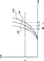
图11说明了监测元件的V-I特性的温度依赖性.Figure 11 illustrates the temperature dependence of the V-I characteristic of the monitoring element.
图12说明了监测元件的V-I特性由于其退化而随时间的变化.Figure 12 illustrates the V-I characteristics of the monitoring element as a function of time due to its degradation.
图13为具有补偿电路的无源矩阵显示装置的示意性图示.13 is a schematic illustration of a passive matrix display device with a compensation circuit.
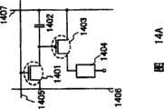
图14A和14B说明了适用于本发明的有源矩阵显示装置的像素配置的示例.14A and 14B illustrate examples of pixel configurations suitable for active matrix display devices of the present invention.
图15A和15B分别说明了有源矩阵显示装置的面板结构.15A and 15B respectively illustrate the panel structure of an active matrix display device.
图16A和16B分别说明了无源矩阵显示装置的面板结构.16A and 16B respectively illustrate the panel structure of a passive matrix display device.
图17A和17B说明了适用于有源矩阵显示装置的发光元件的示例.17A and 17B illustrate examples of light emitting elements suitable for active matrix display devices.
图18说明了适用于有源矩阵显示装置的发光元件的示例.Figure 18 illustrates an example of a light emitting element suitable for an active matrix display device.
图19A和19B说明了适用于无源矩阵显示装置的发光元件的示例.19A and 19B illustrate examples of light emitting elements suitable for passive matrix display devices.
图20说明了适用于无源矩阵显示装置的发光元件的示例.Figure 20 illustrates an example of a light emitting element suitable for a passive matrix display device.
图21A至21H说明了可以应用本发明显示装置的电子设备.21A to 21H illustrate electronic equipment to which the display device of the present invention can be applied.
具体实施方式Detailed ways
尽管将参照附图通过实施方式和实施例全面地描述本发明,但是应该理解,对于本领城技术人员而言各种变化和改进是显而易见的.因此,除非这些变化和改进偏离本发明的范围,否则应将这些变化和改进理解为包含在该范围内.Although the present invention will be fully described by means of embodiments and examples with reference to the accompanying drawings, it should be understood that various changes and improvements will be apparent to those skilled in the art. Therefore, unless these changes and improvements depart from the scope of the present invention, Otherwise such changes and improvements should be construed as being included within the scope.
[实施方式1][Embodiment 1]
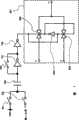
下面参照图1,对包含在本发明显示装置内的温度/退化补偿电路(下文中简称为补偿电路)的基本原理进行描述.1, the basic principle of the temperature/degradation compensation circuit (hereinafter simply referred to as the compensation circuit) included in the display device of the present invention will be described.
基本电流源101向监测元件102供给恒定电流.即,监测元件102受恒定电流驱动.因此,监测元件102的电流值一直保持恒定.当环境温度在这些条件下改变时,监测元件102的电阻值本身发生变化.当监测元件102的电阻值改变时,监测元件102的相反电极之间的电势差改变,因为其电流值恒定.通过检测监测元件102的相反电极之间的电势差,检测环境温度的变化.具体而言,固定在恒定电势的监测元件102的一个电极的电势,即图1中阴极的电势没有变化.因此,连接到电流源101的监测元件102的另一个电极的电势变化,即图1中阳极103的电势被检测.The basic
这里,参照图11描述监测元件102的V-I特性的温度依赖性.监测元件102在室温(例如25℃)、低温(例如-20℃)和高温(例如70℃)下的V-I特性分别用线1101、1102和1103表示.假设从电流源101流到监测元件102的电流值为I0,室温下在监测元件102内产生电压V0.同时,在低温下产生电压V1,在高温下产生电压V2.即,当电流I0在室温下流过监测元件102时,电压降落到V0;当电流I0在低温下流过监测元件102时,电压降落到V1;当电流I0在高温下流过监测元件102时,电压降落到V2.因此,当环境温度降低时通过对发光元件115施加电压V1,而当环境温度变高时对发光元件115施加电压V2,即可对温度进行补偿.Here, the temperature dependence of the VI characteristic of the
图12说明了监测元件102的V-I特性随时间的变化.监测元件102的初始特性用线1201表示,而退化的监测元件102的特性用线1202表示.注意,这里假设在相同的温度条件(室温)下测量该初始特性和退化后的特性.在初始特性的条件下当电流I0流到监测元件102时,在监测元件102内产生电压V0,而在已经退化的监测元件102内产生电压V3.因此,如果将电压V3施加到已经类似地退化的发光元件115,则发光元件115的表观退化可以减小.Figure 12 illustrates the VI characteristics of the
根据本发明,基于有关环境温度以及随时间的退化的数据而产生的电压被施加到发光元件115.即,根据由于环境温度变化以及随时间的退化而导致的发光元件115的电阻值变化,设定该电压值.按照这种方式,由于环境温度变化以及随时间的退化而导致的发光元件115的亮度变化得到抑制.此外,预先设定特定的条件,当满足该条件时切换电压源.由此可以提供稳定的电压源.According to the present invention, a voltage generated based on data on ambient temperature and degradation over time is applied to the light-emitting
下面进行更详细的描述.首先,连接开关106的端子a和c.此时,监测元件102的阳极103的电势输入到放大器104,且进行阻抗转换.接着,放大器104输出与阳极103的电势相同的电势,该电势随后输入到驱动晶体管114的源极端.因此,当驱动晶体管114导通时,在监测元件102内产生的电压施加到发光元件115.因此,通过实际上使用恒定电压驱动该显示装置,可以表观地执行发光元件115的恒流驱动.即,由于温度变化以及随时间的退化所致的电流值的波动可以得到抑制.注意在图1中,监测元件102的阴极和发光元件115的阴极连接到接地电势GND;然而,本发明不限于此,只要监测元件102的阴极和发光元件115的阴极的电势相同即可.A more detailed description is carried out below. First, the terminals a and c of the
同时,包括在监测元件102内产生的电压的模拟数据此时在A/D转换器107内被转换成数字数据,且随后输入到电压数学处理电路108.温度特性检测监测电路111监测温度,且将检测的温度数据输入电压数学处理电路108。此外,由计数器电路113计数的有关监测元件102发光时间段的数据被输入到电压数学处理电路108.基于这些数据,电压数学处理电路108根据每个温度条件对电压进行数学处理.接着,经过数学处理的数据存储于存储器电路112。Meanwhile, the analog data including the voltage generated in the
基于通过获得存储于存储器电路112内的监测元件102的电压变化的数学公式、由温度特性检测监测电路111监测的温度条件、以及从计数器电路113输入的时间条件而得到的数据,电压数学处理电路108计算将被施加到发光元件115的电压.通过这样计算得到的电压的数字数据输入到D/A转换器电路109.接着,该数据被D/A转换器电路109转换成模拟电压.此外,该模拟电压的数据被放大器110进行阻抗转换.按照该方式,通过补偿由于温度变化以及随时间的退化引起的电流值变化而得到的电势也被输入到开关106的端子b.Based on the data obtained by obtaining the mathematical formula of the voltage change of the
接着,当预设条件满足时,开关106的连接被切换.即,开关106的端子a和c被断开,而其端子b和c被连接.按照该方式,施加于发光元件115的电压被切换到由外推电源电路105所产生的电压,外推电源电路105从检测监测元件102的电势并在放大器104内阻抗转换该电势之后输入的电压产生所述电压.Then, when the preset condition is satisfied, the connection of the
图2A说明了发光元件115内产生的电压的变化.线201a表示室温下的电压变化,线201b表示低温下的电压变化,线201c表示高温下的电压变化.logt0之前的实线表示监测元件102的阳极103的电势的实际测量值,而logt0之后的虚线表示基于阳极103的采样电势变化,通过估计随时间变化的监测元件102的电压而得到的数学处理值.即,外推电源电路105对监测元件102的阳极103的电势变化进行采样直至1ogt0,从而采用内插方法等执行数学处理.换而言之,得到表达监测时段102的累计发光时间段和施加到监测元件102的电压之间关系的数学公式.在logt0之后,外推电源电路105产生由该数学公式得到的电压.对于图2A的情形,测量实际测量数据直至logt0,通过估计来数学处理之后的电压变化.此外,根据每个温度条件得到并数学处理实际测量数据.即,通过根据每个温度条件使用温度特性检测监测电路111监测温度,数学处理监测元件102的阳极103的电压变化.Figure 2A illustrates the change in voltage generated within the light-emitting
备选地,如图2B所示,可通过测量有关监测元件102的阳极103的实际电势值的数据,直到升高至特定电压VDD2为止,来数学处理所述电压变化。注意,线202a表示常温下的电压变化,线202b表示低温下的电压变化,线202c表示高温下的电压变化.Alternatively, as shown in FIG. 2B , the voltage variation can be mathematically processed by measuring data on the actual potential value of the
通过像本发明一样切换电压源,即使当监测元件102连续使用并因此损坏时,仍可以将电压供给到发光元件.此外,由于可以根据发光元件在各个温度条件下的特性变化而供给电压,可以补偿温度和退化.By switching the voltage source like the present invention, even when the
此外,通过将开关106置于放大器301的输入端侧,如图3所示,可以使用一个放大器301替代放大器104和放大器110.此外,使用运算放大器的电压输出器电路可以应用于放大器104和110,同样可以应用于放大器301.这是因为电压输出器电路的不倒相输入端具有高的输入阻抗,而其输出端具有低的输出阻抗,这使得输入端和输出端可具有相同或者基本上相同的电势,由此可以从该输出端供给电流,而不需要从电流源101流到电压输出器电路的电流.即,可以实施阻抗转换.因此,不言而喻,本发明不限于电压输出器电路,只要提供了具有这种功能的电路即可.此外,不一定需要由放大器104和110或者放大器301执行该阻抗转换,只要可替代的放大器从输出端输出与输入到输入端的电势基本上相同的电势即可.因此,电压反馈放大器或者电流反馈放大器可以恰当地用于放大器104、110和301.In addition, by placing the
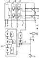
接着参照图4描述具有补偿功能的显示装置的具体配置.该显示装置包括源极信号线驱动电路401、栅极信号线驱动电路402和像素部分403.像素部分403具有多个像素413.该显示装置还包括监测元件组404、基本电流源405、外推电源电路406、放大器407和开关408.将电流从基本电流源405供给到监测元件组404.接着,在包含于监测元件组404的各个监测元件中发生电压降落.即,由于包含于监测元件组404内的各个监测元件具有电阻值,发生电压降.监测元件组404的监测元件的阴极连接到GND;因此,通过检测阳极409的电势,可以得到有关监测元件组404的监测元件中产生的电压的数据.注意,如图4所示通过提供多个监测元件,由于各个监测元件的电阻值变化导致的电压降的变化可以被平均化.此外,根据特定条件(例如电压变化或时间变化)切换开关408的连接,且外推电路406基于通过获得监测元件组404内产生的电压的变化的数学公式而得到的数据,确定将被供给到电源线V1至Vm的电势。省略了其详细操作,因为已经参考图1和3进行了描述.Next, a specific configuration of a display device having a compensation function is described with reference to FIG. 4. The display device includes a source signal
源极信号线驱动电路401包括脉冲输出电路410、第一锁存电路411、和第二锁存电路412.SCK信号、SCKB信号和SSP信号输入到脉冲输出电路410,且脉冲输出电路410的输出信号依次输入到对应于源极信号线S1至Sm的第一锁存电路411.接着,DATA信号串行输入到第一锁存电路411.串行DATA信号被第一锁存电路411根据依次从脉冲输出电路410输入的信号并行地锁存于各级中.接着,并行锁存的DATA信号在SLAT信号输入时被传输到第二锁存电路412.接着,并行保持的DATA信号被写入连接到选定的栅极信号线的像素.The source signal
以下描述开关的配置及其工作原理,该开关可以作为图1和3所示具有三个端子的开关106和如图4所示的开关408.The following describes the configuration and working principle of the switch, which can be used as a
图5说明了经过特定时间段之后,用于切换电源的开关的示例.开关501包括模拟开关502、模拟开关503和反相器504.由判定电路506产生用于控制开关501的控制信号.由计数器电路505对时钟信号进行计数,且其数据作为信号输入到判定电路506.接着,在判定电路506中对记录于判定参考值存储器(存储判定参考值的存储器)中的信号与来自计数器电路505的信号进行比较.当判定参考值存储器507的信号值大于计数器电路505的信号值时,判定电路506输出L-level信号,由此使模拟开关502断开且模拟开关503导通.即,开关501的端子a和c相连接,直到计数器电路505的信号值超过判定参考值存储器507的值(即,直到经过某一时间段为止).接着,当计数器电路505的信号值大于存储于判定参考值存储器507内的值时,H-level从判定电路506输出,由此使模拟开关502导通且模拟开关503断开.即,经过某一时间段之后,开关501的端子b和c相连接.按照该方式,经过预设时间后,发光元件的电压源可以切换到外推电源电路105或406。Figure 5 illustrates an example of a switch for switching a power supply after a certain period of time has elapsed. The
以下参照图6和7描述具有三个端子的开关的工作,其中在输入电势超过某一电压值之后,电源被切换.开关501的配置类似于图5中的开关501,因此省略了对其的描述.这种情况下,运算放大器601可以作为控制信号的发生器.监测元件的阳极的电势作为输入电势被输入到运算放大器601的不倒相输入端.同时,参考电势被输入到其反相输入端。这里,图2B所示的电势VDD2被输入作为参考电势.因此,如果输入电势低于VDD2,则运算放大器601输出L-level信号,由此使模拟开关502断开且模拟开关503导通.即,开关501的端子a和c相连接.当输入电势高于VDD2时,运算放大器601输出H-level信号,由此使模拟开关502导通且模拟开关503断开.即,开关501的端子b和c相连接.按照该方式,当输入电势超过预设电势(图6中的VDD2)时,发光元件的电压源可以被切换到外推电源电路105或406.The operation of a switch with three terminals, in which the power source is switched after the input potential exceeds a certain voltage value, is described below with reference to FIGS. 6 and 7. The configuration of the
此外,如图7所示,可以由斩波反相比较器(chopper invertercomparator)替代图6的运算放大器产生控制信号.首先,开关704导通,从而将反相器705的输入端和输出端短路.接着,反相器705被偏移抵消(offset-cancelled),由此使其输入端和输出端具有相同的电势.随后,在该状态下,开关701导通.接着,与被偏移抵消的反相器705的电势与参考电势VDD2之间的电势差相对应的电荷累积于电容器703中.当开关701断开时,电容器703保持该电势差.接着,开关704断开,且开关702导通.接着,当输入电势低于预设电势VDD2时,反相器705的输入端的电势低于使反相器705偏移抵消的电势,因为该电势差被保持于电容器703内.即,L-level信号被输入到反相器705的输入端,H-level信号从其输出端输出,且该信号进一步被反相器706反相.因此,L-level信号作为控制信号输入开关501.此时,模拟开关502断开且模拟开关503导通.因此,开关501的端子a和c相连接.另一方面,如果输入电势高于参考电势VDD2,则反相器705的输入端高于使反相器705偏移抵消的电势,因为该电势差被保持于电容器703内.接着,H-level信号输入到反相器705,该信号在反相器706内被反相.因此,H-level信号作为控制信号输入到开关501.接着,模拟开关502导通且模拟开关503断开.因此,开关501的端子b和c相连接.按照该方式,当监测元件的电势变为高于预设电势(图7中的VDD2)时,发光元件的电压源可以切换到外推电源电路105或406.In addition, as shown in Figure 7, the operational amplifier in Figure 6 can be replaced by a chopper inverter comparator to generate the control signal. First, the
像本发明这样的具有温度补偿功能和退化补偿功能的这种驱动方法也称为恒定亮度.This driving method with temperature compensation function and degradation compensation function like the present invention is also called constant brightness.
注意,可以恰当地选择监测元件的数目.不言而喻,可以提供单个监测元件或如图4所示的多个监测元件.当使用单个监测元件时,流到基本电流源101的电流可以设定为具有将被供给到各个像素内发光元件的电流值;因此可以降低功耗.Note that the number of monitoring elements can be chosen appropriately. It goes without saying that a single monitoring element or a plurality of monitoring elements as shown in FIG. 4 can be provided. When a single monitoring element is used, the current flowing to the basic
此外,本发明不限于图4中的配置,可以采样这样的配置,即,使得监测元件置于源极信号线驱动电路侧上,置于跨过像素部分与栅极信号线驱动电路相对的一侧上,或者置于跨过像素部分与源极信号线驱动电路相对的一侧上.为了有效地实现温度补偿功能,可以恰当地选择监测元件的位置.In addition, the present invention is not limited to the configuration in FIG. 4, and a configuration may be sampled such that the monitoring element is placed on the side of the source signal line driver circuit, placed on a side opposite to the gate signal line driver circuit across the pixel portion. On the side, or on the side opposite to the source signal line driver circuit across the pixel portion. In order to effectively realize the temperature compensation function, the position of the monitoring element can be properly selected.
监测元件和发光元件优选地使用相同材料同时形成于相同基板上.这是因为可以减小监测元件和发光元件的V-I特性的差异.The monitoring element and the light emitting element are preferably simultaneously formed on the same substrate using the same material. This is because the difference in V-I characteristics of the monitoring element and the light emitting element can be reduced.
注意,如图4的公共电势输入到电源线V1至Vm的配置,优选应用于单色显示装置或者应用于与白光发射元件及滤色器组合可以全色显示的显示装置.Note that the configuration in which the common potential is input to the power supply lines V1 to Vm as in FIG. 4 is preferably applied to a monochrome display device or to a display device capable of full-color display in combination with a white light emitting element and a color filter.
此外,可以为每个RGB像素设定电源线的电势.图8说明了这种情形的示例。图8中的显示装置包括源极信号线驱动电路801、栅极信号线驱动电路802、以及包括多个像素809的像素部分803.In addition, the potential of the power supply line can be set for each RGB pixel. Figure 8 illustrates an example of this situation. The display device in FIG. 8 includes a source signal
连接到发R(红)光像素的源极信号线用信号源极线Sr1至Srm表示.连接到发G(绿)光像素的源极信号线用源极信号线Sg1至Sgm表示.连接到发B(蓝)光像素的源极信号线用源极信号线Sb1至Sbm表示.The source signal lines connected to the pixels emitting R (red) light are indicated by signal source lines Sr1 to Srm. The source signal lines connected to the pixels emitting G (green) light are indicated by source signal lines Sg1 to Sgm. The source signal lines of the pixels emitting B (blue) light are represented by source signal lines Sb1 to Sbm.
这里,电流源805r将电流供给到监测元件804r1至804rn,电压输出器电路807r检测监测元件804r1至804rn的阳极的电势.接着,所检测电势输入到电源线Vr1至Vrm.电流源805g将电流供给到监测元件804g1至804gn,电压输出器电路807g检测监测元件804g1至804gn的阳极的电势.接着,所检测电势输入到电源线Vg1至Vgm.电流源805b将电流供给到监测元件804b1至804bn,电压输出器电路807b检测监测元件804b1至804bn的阳极的电势.接着,所检测电势输入到电源线Vb1至Vbm.Here, the
按照该方式,可以为每个RGB像素设定电势.例如,当RGB像素的温度特性或退化特性根据其EL材料而不同时,可以将期望的电势输入到每个发光元件.即,通过设定用于每个RGB像素的电源线的电势,可以校正由于温度变化以及随时间的退化而波动的流入各个发光元件的电流值.此外,假设预设特定条件且该条件满足,则开关808r、808g和808b被切换,使得电势从外推电源电路806r输入到电源线Vr1至Vrm,电势从外推电源电路806b输入到电源线Vg1至Vgm,且电势从外推电源电路806b输入到电源线Vb1至Vbm.按照该方式,即使在显示装置连续使用,导致监测元件804r1至804rn、804g1至804gn和804b1至804bn损坏时,电势仍从外推电源电路806r、806g和806b分别输入到电源线Vr1至Vrm、Vg1至Vgm和Vb1至Vbm.因此显示装置可以正常工作.此外,通过从外推电源电路806r、806g和806b输入电势,可以校正由于温度变化以及随时间的退化而波动的发光元件的电流值.In this way, the potential can be set for each RGB pixel. For example, when the temperature characteristics or degradation characteristics of RGB pixels differ according to their EL materials, a desired potential can be input to each light emitting element. That is, by setting The potential of the power supply line for each RGB pixel can correct the current value flowing into each light emitting element fluctuating due to temperature change and degradation with time. Furthermore, assuming that a certain condition is preset and satisfied, the
接着描述可以用于该实施方式的显示装置的像素配置.注意,本发明不限于图4和8所示像素配置,可以应用其中使用了电压驱动类型的晶体管作为像素晶体管的其他像素配置.即,本发明可以应用于具有如下像素配置的显示装置,该像素配置中工作于线性区域的晶体管用作发光元件的驱动晶体管.Next, a pixel configuration that can be used in the display device of this embodiment mode is described. Note that the present invention is not limited to the pixel configuration shown in FIGS. The present invention can be applied to a display device having a pixel configuration in which a transistor operating in a linear region is used as a driving transistor of a light emitting element.
首先,参照图14A描述图4和8所示显示装置的像素配置的工作.该像素包括开关晶体管1401、电容器1402、驱动晶体管1403、发光元件1404、栅极信号线1405、源极信号线1406和电源线1407.开关晶体管1401的栅极端连接到栅极信号线1405.开关晶体管1401的源极端连接到源极信号线1406,而其漏极端连接到驱动晶体管1403的栅极端.此外,电容器1402的一个端子连接到驱动晶体管1403的栅极端,而其另一个端子连接到电源线1407.驱动晶体管1403的源极端还连接到电源线1407,其漏极端连接到发光元件1404的阳极.当开关晶体管1401被从栅极信号线1405输入的信号导通时,数字视频信号从源极信号线1406输入到驱动晶体管1403的栅极端.输入的数字视频信号的电压保持于电容器1402内.通过该输入的数字视频信号,选择驱动晶体管1403的导通/断开,从而控制是否将从电源线1407输入的电势输入到发光元件1404的阳极.通过根据本发明设定电源线1407的电势,可以校正由于温度变化以及随时间的退化而波动的发光元件1404的电流值.此外,可以提供稳定的电压源.First, the operation of the pixel configuration of the display device shown in FIGS. 4 and 8 will be described with reference to FIG. 14A. The pixel includes a
此外,本发明可以应用于具有图14B所示像素配置的显示装置.图14B的配置对应于通过对图14A的配置另外提供擦除晶体管1408和擦除信号线1409而实现的配置.因此,图14A和14B之间的共同部分使用相同参考数字表示.在该配置中,当擦除信号输入到擦除信号线1409以导通擦除晶体管1408时,保持于电容器1402内的电荷被释放以断开驱动晶体管1403,由此发光元件1404可变得不发光.此外,在该配置中,通过根据本发明设定电源线1407的电势,可以校正由于温度变化以及随时间的退化而波动的发光元件1404的电流值.此外,可以提供稳定的电压源.In addition, the present invention can be applied to a display device having a pixel configuration shown in FIG. 14B. The configuration of FIG. 14B corresponds to a configuration realized by additionally providing an erasing
此外,本发明不限于前述配置,且本发明可以应用于其中像素内晶体管的导电类型改变、连接改变、或者提供附加晶体管的像素配置.Furthermore, the present invention is not limited to the foregoing configuration, and the present invention can be applied to a pixel configuration in which the conductivity type of transistors within a pixel is changed, the connection is changed, or an additional transistor is provided.
[实施方式2][Embodiment 2]
在实施方式1中,描述了有源矩阵显示装置(也称为有源显示装置);然而,本发明还可以应用于无源矩阵显示装置(也称为无源显示装置).因此,在该实施方式中,描述本发明的补偿电路应用于无源矩阵显示装置的情形.In
以下参考图9描述列信号线驱动电路和补偿电路的配置和工作.图9所示的列信号线驱动电路913可以控制从温度/退化补偿电路(下文中简称为补偿电路)输入的电势被输出到列信号线S1、S2...的时间段,由此可以执行时间灰度级显示.The configuration and operation of the column signal line driver circuit and the compensation circuit are described below with reference to FIG. 9. The column signal
首先,连接开关906的端子a和c.接着,电流源901将恒定电流供给到监测元件902.即,使用恒定电流驱动监测元件902.接着,监测元件902的阳极903的电势被放大器904检测,并输出到列信号线S1、S2....注意,放大器904可以是例如电压输出器电路.First, the terminals a and c of the
此外,从脉冲输出电路914输出脉冲,DATA信号根据该脉冲依次保持于第一锁存电路915内.接着,在SLAT信号输入时,保持于第一锁存电路915内的数据传输到第二锁存电路916.接着,保持于第二锁存电路916内的数据控制开关917a1、917a2...的导通时间段,由此设定将电势供给到列信号线S1至Sn的时间段,即,将电势供给到发光元件的时间段.按照该方式,可以执行时间灰度级显示。In addition, a pulse is output from the
注意,例如对于实际显示3位灰度级的情形,第一锁存电路915和第二锁存电路916分别具有三个锁存电路.接着,从第二锁存电路916输出的3位数据被转换成具有针对显示8级灰度级情形的脉冲宽度的信号,且开关917a1、917a2...在所述脉冲宽度的时间段内被导通.按照该方式可以显示8级灰度级.Note that, for example, for the case of actually displaying 3-bit grayscale, the
此外,根据预设条件,切换开关906的连接,由此使由外推电源电路905产生的电压被放大器904阻抗转换,从而电势被输入到列信号线.Furthermore, according to preset conditions, the connection of the
注意,包括在监测元件902内产生的电压的模拟数据在A/D转换器电路907内被转换为数字数据,且随后输入到电压数学处理电路908.温度特性检测监测电路910监测温度,且将检测的温度数据输入电压数学处理电路108.此外,与由计数器电路912计数的监测元件902发光时间段有关的数据被输入到电压数学处理电路908.基于这些数据,电压数学处理电路908根据各个温度条件对电压进行数学处理.接着,经过数学处理的电压存储于存储器电路911.基于通过获得存储于存储器电路911内的监测元件902的电压变化的数学公式、由温度特性检测监测电路910监测的温度条件、以及从计数器电路912输入的时间条件而得到的数据,电压数学处理电路908计算将被输入到列信号线S1、S2...的电压.通过计算得到的电压的数字数据被D/A转换器电路109转换成模拟电压.按照该方式,可以减小由于温度变化以及随时间的退化引起的流入发光元件的电流值波动.Note that analog data including the voltage generated in the
图10说明了图9的列信号驱动电路应用于显示装置的示例.该显示装置包括列信号线驱动电路1001、行信号线驱动电路1002和像素部分1003.通过行信号线驱动电路1002,选择行信号线V1至Vm之一.即,一个行信号线设定为使得,通过输入到行信号线和列信号线的电势之间的电势差,电流流到发光元件1009.接着,输入到选定行信号线和列信号线的电势之间的电势差施加到介于该行信号线和列信号线之间的发光元件1009.于是发光元件1009由于电流而发光.此时,尽管输入到列信号线S1至Sn中每个的电势设定为具有相同电平,但是输入电势的时间段不同.按照该方式可以执行时间灰度级显示.Figure 10 illustrates an example in which the column signal driving circuit of Figure 9 is applied to a display device. The display device includes a column signal
在本发明中,恒定电流从电流源1004供给到监测元件1007.即,执行恒定电流驱动。开关1008的端子a和c相连接,直到满足预设条件(例如时间或电压)为止.接着,监测元件1007的阳极1010的电势被检测,由此通过电压输出器电路1006设定供给到列信号线的电势.按照该方式,可以提供具有温度和退化补偿功能的显示装置.In the present invention, a constant current is supplied from the
接着,当预设条件满足时,开关1008的连接被切换,由此开关1008的端子b和c相连接.接着,由外推电源电路1005产生的电势通过电压输出器电路1006输入到列信号线S1至Sn.Next, when the preset condition is satisfied, the connection of the
按照该方式,通过切换电压源,即使在监测元件1007由于其连续使用而损坏时,该显示装置仍可正常工作.此外,可以根据各个温度条件对监测元件1007内产生的电压随时间的变化进行数学处理,外推电源电路1005基于此产生电势.因此可以补偿温度和退化导致的变化.In this way, by switching the voltage source, even when the
注意,可以恰当地选择监测元件的数目.不言而喻,可以提供如图10所示的单个监测元件或者多个监测元件.当使用单个监测元件时,电流源1004只需要设定将被供给到各个像素内的发光元件1109的电流值;因此可以降低功耗.Note that the number of monitoring elements can be chosen appropriately. It goes without saying that a single monitoring element as shown in Figure 10 or a plurality of monitoring elements can be provided. When a single monitoring element is used, the
备选地,多个监测元件可以并联连接,或者可以提供与行信号线相同数目的监测元件,这种情况下监测元件的阴极分别连接到行信号线.此外,可以采样这样的配置,即,使得监测元件置于行信号线驱动电路侧或列信号线驱动电路侧,置于跨过像素部分与行信号线驱动电路相对的一侧,或者置于跨过像素部分与列信号线驱动电路相对的一侧.为了有效地实现温度补偿功能,可以恰当地选择监测元件的位置.Alternatively, multiple monitoring elements can be connected in parallel, or the same number of monitoring elements as the row signal lines can be provided, in which case the cathodes of the monitoring elements are respectively connected to the row signal lines. Furthermore, such a configuration can be sampled that, The monitoring element is placed on the side of the row signal line driver circuit or the side of the column signal line driver circuit, placed on the side across the pixel portion opposite to the row signal line driver circuit, or placed across the pixel portion opposite to the column signal line driver circuit One side. In order to effectively realize the temperature compensation function, the position of the monitoring element can be properly selected.
监测元件和发光元件优选使用相同材料同时形成于相同基板上.这是因为可以减小监测元件和发光元件的V-I特性的差异.The monitoring element and the light emitting element are preferably formed on the same substrate at the same time using the same material. This is because the difference in V-I characteristics of the monitoring element and the light emitting element can be reduced.
注意,如图10的公共电势输入到每个列信号线的配置,优选应用于单色显示装置,或者与白光发射元件及滤色器组合可以全色显示的显示装置.Note that the configuration in which the common potential is input to each column signal line as in FIG. 10 is preferably applied to a monochrome display device, or a display device that can display full colors in combination with a white light emitting element and a color filter.
此外,可以将连接到电源线的像素的电势设定为对应于RGB颜色.图13说明了这种情形的示例.Furthermore, the potentials of the pixels connected to the power lines can be set to correspond to RGB colors. Figure 13 illustrates an example of this situation.
图13中的显示装置包括列信号线驱动电路1301、行信号线驱动电路1302、以及包括R(红色)像素1309r、G(绿色)像素1309g和B(蓝色)像素1309b的像素部分1303.The display device in FIG. 13 includes a column signal
连接到发R(红)光像素的信号线用信号线Sr1至Srm表示.连接到发G(绿)光像素的信号线用信号线Sg1至Sgm表示.连接到发B(蓝)光像素的信号线用信号线Sb1至Sbm表示.The signal lines connected to the R (red) light emitting pixels are represented by signal lines Sr1 to Srm. The signal lines connected to the G (green) light emitting pixels are represented by signal lines Sg1 to Sgm. The signal lines connected to the B (blue) light emitting pixels are represented by signal lines Sg1 to Sgm. The signal lines are represented by signal lines Sb1 to Sbm.
简要描述图13中列信号线驱动电路的工作.从脉冲输出电路1310输出脉冲,根据所述脉冲,DATA信号依次输入第一锁存电路1311.接着,保持于第一锁存电路1311内的数据在SLAT信号输入时被传输到第二锁存电路1312.接着,保持于第二锁存电路1312的数据控制开关1313的导通时间段,由此设定用于将电压输出器1307r、1307g和1307b的输出分别供给到列信号线Sr1至Srn、Sg1至Sgn和Sb1至Sbn的时间段(即,在一个水平周期内发光元件的发光时间段).接照该方式,可以执行时间灰度级显示.Briefly describe the operation of the column signal line driver circuit in Figure 13. The pulse is output from the
在本发明中,电流源1304r、1304g和1304b分别使恒定电流流到监测元件组1308r、1308g和1308b.即,使用恒定电流驱动监测元件组1308r、1308g和1308b.于是,各个开关1306r、1306g和1306b的端子a和c相连接,直到满足预设条件(例如时间或电压)为止.接着,监测元件组1308r、1308g和1308b的阳极的电势分别被检测,由此通过电压输出器1307r、1307g和1307b设定供给到列信号线的电势.按照该方式,可以提供具有温度和退化补偿功能的显示装置.In the present invention, the
按照该方式,可以为每个RGB像素设定电势.例如,当RGB像素的温度特性或退化特性根据EL材料而不同时,可以将期望的电势输入到每个发光元件.即,可以为每个RGB像素设定和校正列信号线的电势.In this way, the potential can be set for each RGB pixel. For example, when the temperature characteristics or degradation characteristics of the RGB pixels differ depending on the EL material, a desired potential can be input to each light emitting element. That is, it is possible to set the potential for each The RGB pixels set and correct the potential of the column signal lines.
此外,假设预设条件满足,则开关1306r、1306g和1306b的连接被切换,由此其端子b和c相连接.于是,由外推电源电路1305r、1305g和1305b产生的电势分别从电压输出器电路1307r、1307g和1307b输入到列信号线Sr1至Srn、Sg1至Sgn和Sb1至Sbn.Furthermore, assuming that the preset conditions are satisfied, the connections of the
按照该方式,通过切换电压源,即使在由于其连续使用而导致监测元件组1308r、1308g和1308b损坏时,该显示装置仍可以正常工作。此外,根据每个温度条件对监测元件组1308r、1308g和1308b内产生的电压随时间的变化进行数学处理,外推电源电路1305r、1305g和1305b基于此产生电压.因此可以补偿温度和退化.In this way, by switching the voltage source, even when the
在图13的配置中,仅一个监测元件连接到一条行信号线,监测元件组1308r、1308g和1308b中包含的每个监测元件的阴极连接到该行信号线,因此仅一个监测元件为一个RGB像素发光.然而,当将监测元件组1308r、1308g和1308b内包含的每个监测元件并联连接到RGB像素时,每个RGB(像素)的监测元件内产生的电压可以被平均.In the configuration of FIG. 13, only one monitoring element is connected to one row signal line, and the cathode of each monitoring element contained in the
[实施方式3][Embodiment 3]
以下描述实施方式1和2所示显示装置的面板结构.The panel structures of the display devices shown in
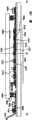
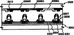
首先描述实施方式1所示显示装置的面板结构的一个示例.图15A为该显示装置的顶视图,而图15B为沿线A-A’-A”的该显示装置的剖面视图.如虚线所示,该显示装置包括驱动电路部分(源极信号线驱动电路)1501、像素部分1502、监测元件部分1503和驱动电路部分(栅极信号线驱动电路)1504.由密封基板1505和密封剂1506围绕的空间对应于空间1507.First, an example of the panel structure of the display device shown in
注意,布线1509是这样的布线,其用于传送输入到源极信号线驱动电路1501或栅极信号线驱动电路1504的信号,并用于从作为外部输入端的FPC(柔性即刷电路)1510接收视频信号、时钟信号、起始信号、复位信号等.IC芯片(半导体集成电路)1511通过COG(玻璃上芯片)接合连接在FPC 1510上.注意,还可以通过TAB(载带自动接合)或通过使用印刷板连接IC芯片1511.Note that the
接着参照图15B描述图15A的剖面结构.在基板1508上形成了源板信号线驱动电路1501、像素部分1502、监测元件部分1503和栅极信号线驱动电路1504.Next, the cross-sectional structure of FIG. 15A will be described with reference to FIG. 15B. A source plate signal
注意,源极信号线驱动电路1501由具有n沟道TFT1512和p沟道TFT 1513的CMOS电路组成.TFT 1525为组成栅极信号线驱动电路1504的TFT.还可以使用已知的CMOS电路、PMOS电路或者NMOS电路形成用于形成该驱动电路的TFT.此外,尽管本实施方式示出了驱动电路形成于基板上的驱动器集成结构,但是本发明不限于此,驱动电路还可以形成于基板外部.Note that the source signal
此外,像素部分1502包括多个像素,每个像素包括开关TFT1514、电流控制TFT 1515以及电连接到该电流控制TFT 1515漏极的第一电极1516.注意,形成了覆盖第一电极1516边缘的绝缘体1517.这里,绝缘体1517由正光敏丙烯酸树脂膜形成.In addition, the
此外,为了提高覆盖度,绝缘体1517的顶端或底端形成为具有有曲率的弯曲表面.例如,对于绝缘体1517的材料使用正光敏丙烯酸树脂的情形,优选地仅绝缘体1517的顶端具有弯曲表面,该弯曲表面具有曲率半径(0.2至3μm).此外,可以使用通过曝光不溶解于蚀刻剂的负光敏材料或者通过曝光溶解于蚀刻剂的正光敏材料形成绝缘体1517.In addition, in order to improve coverage, the top or bottom of the
在第一电极1516上形成电致发光层1518和第二电极1519.这里,期望由具有高功函数的材料形成用作阳极的第一电极1516.例如,可以使用例如钛膜、铬膜、钨膜、Zn膜或Pt膜的单层膜,以及氮化钛膜和含铝为主要成分的膜的叠层结构,氮化钛膜、含铝为主要成分的膜以及氮化钛膜的三层结构等形成该第一电极1516.注意,当第一电极1516形成为具有叠层结构时,作为布线的电阻可以得到抑制,可以得到极好的欧姆接触且第一电极可以作为阳极.An
通过使用蒸镀掩模的气相沉积或者喷墨沉积形成电致发光层1518.使用元素周期表的第四族的金属络合物部分地形成电致发光层1518,低分子量或高分子量的材料可以与该金属络合物组合.一般而言,经常使用有机化合物将该电致发光层形成为单层或者叠层;然而,在本发明中,由有机化合物形成的膜可以部分包含无机化合物.此外,还可以使用已知的三重态发光材料.The
此外,作为形成于电致发光层1518上的第二电极1519的材料,可以使用具有低功函数的材料(例如Al、Ag、Li或Ca,或者其合金,例如MgAg、MgIn、AlLi,或者其化合物CaF2和CaN).注意,这里的显示面板具有顶部发光结构;因此,第二电极1519优选形成为厚度为1至10nm的铝膜、含少量Li的铝膜或者薄金属膜、以及透光导电膜(例如ITO(氧化铟锡)、IZO(氧化铟锌)、ZnO(氧化锌))的叠层.In addition, as the material of the
形成监测元件1523,其具有如下结构,电致发光层1518置于布线1521、连接到部分1521的阳极1522以及第二电极1519之间,其中布线1521使用与电学连接到像素部分1502内电流控制TFT 1515的漏极的第一电极1516相同的材料形成.注意,光屏蔽膜1524形成于监测元件部分1503上,从而屏蔽从监测元件1523发出的光.A
此外,通过使用密封剂1506将密封基板1505粘合到元件基板1508,得到这样的结构,即,由元件基板1508、密封基板1505和密封剂1506围绕的空间1507设有电致发光元件1520和监测元件1523.注意,除了使用惰性气体(例如氮气或氢气)填充空间1507的结构之外,可以采用使用密封剂1506填充空间1507的结构.Furthermore, by bonding the
注意,密封剂1506优选由环氧树脂形成.此外,期望这种材料不应透湿气或氧气.此外,可以使用玻璃基板或石英基板以及由FRP(纤维玻璃增强塑料)、PVF(聚氟乙烯)、丙烯酸等形成的塑料基板,形成密封基板1505.Note that the
按照该方式,可以得到有源矩阵显示装置.In this way, an active matrix display device can be obtained.
注意,图15A和15B说明了顶部发光结构的显示装置的面板;然而,本发明当然可以应用于底部发光结构或者双向发光结构.Note that FIGS. 15A and 15B illustrate a panel of a display device of a top emission structure; however, the present invention can of course be applied to a bottom emission structure or a bidirectional light emission structure.
以下参照图17A描述双向发光结构的发光元件.A light-emitting element with a bidirectional light-emitting structure will be described below with reference to FIG. 17A.
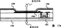
在基板1700上形成电流控制TFT 1701,且第一电极1702形成为与电流控制TFT 1701的漏电极接触,其上形成了包含有机化合物的层1703和第二电极1704.A
第一电极1702为发光元件的阳极.此外,第二电极1704为发光元件的阴极.即,其中包含有机化合物的层1703夹置于第一电极1702和第二电极1704之间的部分对应于该发光元件.The
对于作为阳极的第一电极1702的材料,期望采用具有高功函数的材料.例如可以采用诸如ITO(氧化铟锡)膜和IZO(氧化铟锌)膜的透光导电膜.通过使用这种透光导电膜,可以形成能够透射光的阳极.For the material of the
同时,对于作为阴极的第二电极1704的材料,优选使用由具有低功函数的材料(例如Al、Ag、Li或Ca,或者其合金,例如MgAg、MgIn、AlLi,CaF2或CaN)形成的薄金属膜以及透光导电膜(例如ITO(氧化铟锡)、IZO(氧化锌锡)、ZnO(氧化锌))的叠层.通过使用这种薄金属膜和透光导电膜,可以形成能够透射光的阴极.Meanwhile, for the material of the
按照该方式,如图17A中箭头所示,可以将来自发光元件的光提取到两侧.即,当图17A所示结构应用于图15A和15B的显示装置的面板时,光可以发射到基板1508和密封基板1505侧.因此,对于在显示装置中使用双向发光结构的发光元件的情形,基板1508和密封基板1505均由透光基板形成.In this way, as shown by the arrow in FIG. 17A, the light from the light-emitting element can be extracted to both sides. That is, when the structure shown in FIG. 17A is applied to the panel of the display device of FIGS. 15A and 15B, the light can be emitted to the
此外,对于提供光学膜的情形,基板1508和密封基板1505均可设有光学膜.In addition, for the case of providing an optical film, both the
以下参照图17B描述底部发光结构的发光元件.The light emitting element of the bottom emission structure will be described below with reference to FIG. 17B.
在基板1710上形成电流控制TFT 1711,且第一电极1712形成为与电流控制TFT 1711的漏电极接触,其上形成包含有机化合物的层1713和第二电极1714.A
第一电极1712为发光元件的阳极.此外,第二电极1714为发光元件的阴极.即,其中包含有机化合物的层1713夹置于第一电极1712和第二电极1714的部分对应于发光元件.The
对于作为阳极的第一电极1712的材料,期望采用具有高功函数的材料.例如可以采用诸如ITO(氧化铟锡)膜和IZO(氧化铟锌)膜的透光导电膜.通过使用这种透光导电膜,可以形成能够透射光的阳极.For the material of the
同时,对于作为阴极的第二电极1714的材料,可以采用由具有低功函数的材料(例如Al、Ag、Li或Ca,例如MgAg、MgIn、AlLi的其合金,或者例如CaF2或CaN的其化合物)形成的金属膜.通过使用这种反光金属膜,可以形成不透射光的阴极.Meanwhile, for the material of the
按照该方式,如图17B中箭头所示,可以将来自发光元件的光提取到底侧.即,当图17B所示结构应用于图15A和15B的显示装置的面板时,光可以发射到基板1508侧.因此,对于在显示装置中使用底部发光结构的发光元件的情形,基板1508由透光基板形成.In this way, as shown by the arrow in FIG. 17B, the light from the light-emitting element can be extracted to the bottom side. That is, when the structure shown in FIG. 17B is applied to the panel of the display device of FIGS. 15A and 15B, the light can be emitted to the
此外,对于提供光学膜的情形,基板1508可设有光学膜.In addition, for the case of providing an optical film, the
此外,本发明还可以应用于通过使用白光发射元件和滤色器实现全色显示的显示装置.In addition, the present invention can also be applied to a display device that realizes full-color display by using white light emitting elements and color filters.
如图18所示,电流控制TFT 1801形成于基板1800上,基底膜1802夹置于二者之间,且第一电极1803形成为与电流控制TFT 1801的漏电极接触,其上形成了包含有机化合物的层1804和第二电极1805.注意,不是必须提供基底膜1802.As shown in FIG. 18, a
第一电极1803为发光元件的阳极.此外,第二电极1805为发光元件的阴极。即,其中包含有机化合物的层1804夹置于第一电极1803和第二电极1805之间的部分对应于发光元件.在图18的结构中,发射白光。在该发光元件上提供红色滤色器1806R、绿色滤色器1806G和蓝色滤色器1806B,由此可以执行全色显示.此外,提供了用于将这些滤色器分隔开的黑矩阵(也称为BM)1807.The
图18的结构可以应用于实施方式1中描述的显示装置,其中公共电势输入到电流源线.像素部分中的发光元件仅仅是白光发射元件.因此,通过使用与像素部分内发光元件相似的材料形成监测元件,可以提供一致的元件特性,这导致了更高精确度的补偿功能.The structure of FIG. 18 can be applied to the display device described in
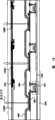
接着参照图16A和16B描述实施方式2所示显示装置的面板结构的示例.注意,图16A为显示装置的顶视图,图16B为沿线B-B’-B”的该显示装置的剖面视图.如虚线所示,该显示装置包括形成于IC芯片1601内的驱动电路部分(列信号线驱动电路)、像素部分1602、监测元件部分1603、和形成于IC芯片1604内的驱动电路部分(行信号线驱动电路).由基板1608、密封基板1605和密封剂1606围绕的空间对应于空间1607.Next, an example of the panel structure of the display device shown in Embodiment Mode 2 will be described with reference to FIGS. 16A and 16B. Note that FIG. 16A is a top view of the display device, and FIG. 16B is a sectional view of the display device along the line BB'-B". As shown by dotted lines, the display device includes a driver circuit part (column signal line driver circuit) formed in an
注意,布线1609是这样的布线,即,用于传送输入到列信号线驱动电路或行信号线驱动电路的信号,并用于从作为外部输入端的FPC(柔性印刷电路)1610接收视频信号、时钟信号、起始信号等.IC芯片(半导体集成电路)1611通过COG(玻璃上芯片)接合,连接到FPC.注意,还可以通过TAB(载带自动接合)或通过使用印刷板连接该IC芯片.Note that the
接着参照图16B描述图16A的剖面结构.在基板1608上形成像素部分1602和监测元件部分1603.列信号线驱动电路部分和行信号线驱动电路部分形成于IC芯片1601和1604上,其通过COG(玻璃上芯片)接合,连接到基板1608.Next, the cross-sectional structure of FIG. 16A is described with reference to FIG. 16B. A
在基板1608上形成基底绝缘膜1612,在该基底绝缘膜上形成叠层的列信号线.下层1613为反光金属膜,上层1614为透光导电氧化物膜.上层1614优选地由具有高功函数的导电膜形成,其包括:透光导电材料,例如氧化铟锡(ITO)以及含Si的ITO(ITSO),和为氧化铟与2至20%氧化锌(ZnO)的混合物的氧化铟锌(IZO);或者组合这些材料的化合物膜.最重要的是,即使进行了烘烤,ITSO也保持为非晶状态,而不像ITO那样会结晶.因此,ITSO在平整度上优于ITO,且即使当含有机化合物的层薄时也不容易导致与阴极的短路,因此适用于发光元件的阳极.A
下层1613由Ag、Al或Al(C+Ni)合金膜形成,最重要的是,Al(C+Ni)膜(包含碳和镍(1至20重量%)的铝合金膜)是优选的,因为即使导电或者施加了热处理之后,其也不会导致Al(C+Ni)膜与ITO或ITSO之间接触电阻值的大的波动.The
用于绝缘相邻的列信号线的分隔壁1618为黑色树脂,其用作与不同颜色的层(设于密封基板一侧)之间的边界交叠或者与间隙交叠的黑矩阵(BM).由黑色分隔壁围绕的区域相应地具有与发光区域相同的面积.The
包含有机化合物的层1615具有从列信号线(阳极)侧依次形成的HIL(空穴注入层)、HTL(空穴输运层)、BML(发光层)、ETL(电子输运层)、EIL(电子注入层)的叠层.注意,包含有机化合物的层1615可具有单层结构或者混合结构以及叠层结构.The
行信号线(阴极)1616形成为与列信号线(阳极)交叉.行信号线(阴极)1616由透光导电膜形成,例如ITO、含Si元素的ITO(ITSO)、以及为氧化铟与2至20%氧化锌(ZnO)的混合物的IZO.本实施方式的结构为顶部发光结构的显示装置的示例,其中光传播穿过密封基板1605;因此,行信号线1616必须透射光.注意,使用正光敏树脂(未曝光部分留下成为图案)通过光刻,以通过控制曝光量和显影时间而使得图案的下部更大程度被蚀刻的方式,形成用于绝缘相邻行信号线的分隔壁1619.The row signal line (cathode) 1616 is formed to cross the column signal line (anode). The row signal line (cathode) 1616 is formed of a light-transmitting conductive film such as ITO, ITO containing Si element (ITSO), and indium oxide with 2 IZO of a mixture of zinc oxide (ZnO) to 20%. The structure of the present embodiment is an example of a display device of a top emission structure in which light propagates through the sealing
按照该方式形成了发光元件1617.In this manner, the
为了保护发光元件1617免受由湿气或者除气引起的损伤,可以提供用于覆盖行信号线1616的透光保护膜.该透光保护膜优选地由通过PCVD得到的致密无机绝缘膜(例如SiN膜或SiNO膜)、通过溅射得到的致密无机绝缘膜(例如SiN膜或SiNO膜)、含碳为主要成分的薄膜(例如DLC膜、CN膜或者非晶碳膜)、金属氧化物膜(例如WO2、CaF2或Al2O3)等形成.注意,“透光的”是指对可见光的透射率为80至100%.In order to protect the light-emitting
在其中形成了监测元件1626的监测元件部分1603上形成光屏蔽膜1620,使得从监测元件部分1603发出的光不会泄漏到外部.A light-shielding
此外,使用密封剂1606和密封基板1605密封包括发光元件的像素部分1602,且由它们围绕的空间1607被气密性密封.In addition, a
密封剂1606可以由紫外固化树脂、热固化树脂、硅酮树脂、环氧树脂、丙烯酸树脂、聚酰亚胺树脂、酚醛树脂、PVC(聚氯乙稀)、PVB(聚乙烯醇缩丁醛)、BVA(乙烯-醋酸乙烯共聚物)等形成.此外,密封剂1606可以添加填充物(条状隔离物或纤维状隔离物)或球形间隔物.The
此外,密封基板1605由玻璃基板或者塑料基板形成.塑料基板可以使用呈板或膜的形式的聚酰亚胺、聚酰胺、丙烯酸树脂、环氧树脂、PES(聚醚砜)、PC(聚碳酸酯)、PET(聚对苯二甲酸乙二酯)和PEN(聚萘二甲酸乙二醇酯)的任意一种.In addition, the sealing
另一方面,基板1608的边缘形成有端电极,用于与外部电路连接的FPC(柔性印刷电路)1610粘结到该端电极.该端电极形成为叠层,下层1613为反光金属膜且与上层1614为透光导电膜;然而本发明并不具体受限于此.On the other hand, a terminal electrode is formed on the edge of the
在像素部分的外围上,分别包括用于传送每个信号到像素部分的驱动电路的IC芯片1601和1604与包括外推电源电路的IC芯片1611通过各向异性导电材料1621电连接到显示面板.此外,为了形成对应于彩色显示的像素部分,XGA类显示面板需要3072条列信号线和768条行信号线.该多个列信号线和行信号线在像素部分的边缘被分为若干块,这些块按照IC输出端子的节距聚集.On the periphery of the pixel portion,
前述显示装置为顶部发光结构的显示装置,且其对比度通过黑色分隔壁1618和1619得以改善.The aforementioned display device is a display device with a top emission structure, and its contrast is improved by the
图16A和16B说明了顶部发光结构的显示装置;然而,不言而喻,本发明可以应用于底部发光结构或双向发光结构.16A and 16B illustrate a display device of a top emission structure; however, it goes without saying that the present invention can be applied to a bottom emission structure or a bidirectional light emission structure.
以下参照图19A描述双向发光结构的发光元件.A light-emitting element with a bidirectional light-emitting structure will be described below with reference to FIG. 19A.
双向发光结构的发光元件包括由透光导电氧化物膜形成的列信号线(阳极)1902、包含有机化合物的层1904和由透光导电氧化物膜形成的行信号线1905.此外,分隔壁1903由光屏蔽材料形成.The light-emitting element of the bidirectional light-emitting structure includes a column signal line (anode) 1902 formed of a light-transmitting conductive oxide film, a
从发光元件发射的光沿图19A中箭头所示方向发射,即沿第一基板1901和第二基板1906的方向发射.因此,第一基板1901和第二基板1906分别由透光基板形成.The light emitted from the light-emitting element is emitted in the direction indicated by the arrow in FIG. 19A, that is, in the direction of the
对于提供光学膜的情形,第一基板1901和第二基板1906均可设有光学膜.For the case of providing an optical film, both the
以下参照图19B描述底部发光结构的发光元件.The light emitting element of the bottom emission structure will be described below with reference to FIG. 19B.
底部发光结构的发光元件包括由透光导电氧化物膜形成的列信号线(阳极)1912、包含有机化合物的层1914和由反光导电膜形成的行信号线1915.此外,分隔壁1913由光屏蔽材料形成.The light-emitting element of the bottom emission structure includes a column signal line (anode) 1912 formed of a light-transmitting conductive oxide film, a
从发光元件发射的光沿图19B中箭头所示方向发光,即沿向着第一基板1911的方向.因此,第二基板1917不特别要求是透光的,其可以是金属板.此外,提供厚的保护膜1916以改善发光元件的可靠性是优选的,因为其不会降低光提取效率.The light emitted from the light-emitting element emits light along the direction indicated by the arrow in FIG. 19B, that is, along the direction toward the
对于提供光学膜的情形,第一基板1911可设有光学膜.For the case of providing an optical film, the
以下参照图20描述分隔壁不是呈倒锥形而是呈正锥形的示例.注意,图20所示结构说明了通过使用白光发射元件和滤色器实现全色显示的示例.An example in which the partition wall is not in the reverse tapered shape but in the forward tapered shape is described below with reference to FIG. 20. Note that the structure shown in FIG. 20 illustrates an example in which full-color display is realized by using white light emitting elements and color filters.
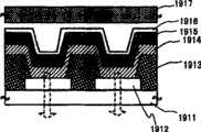
在第一基板2001上形成条形第一电极2002.在该结构中,在第一电极2002上形成具有开口的分隔壁2003,其上形成由第一隔离物2006与宽度大于第一隔离物2006的第二间隔物2007组成的分隔壁.A strip-shaped
第一隔离物2006由例如聚酰亚胺的有机树脂膜形成,第二隔离物2007由例如抗蚀剂的光敏树脂膜形成.例如,首先沉积例如聚酰亚胺的有机树脂膜,在该有机树脂膜上沉积例如抗蚀剂的光敏树脂.接着,在待隔离的电极之间留下例如抗蚀剂的光敏树脂的图案,且暴露的有机树脂被蚀刻.对于该蚀刻,控制蚀刻条件,使得光敏树脂膜的图案被底切(undercut).通过上述步骤,可以形成元件隔离的结构,即分隔壁.The
在图20中,使用光屏蔽材料形成具有开口的分隔壁2003、第一隔离物2006和第二隔离物2007中的每一个,从而改善对比度.In FIG. 20, each of a
在形成分隔壁之后,形成包含有机化合物的层以及透光导电膜,由此可以形成隔离的包含有机化合物的层2004和隔离的第二电极2005.After forming the partition wall, a layer containing an organic compound and a light-transmitting conductive film are formed, whereby an isolated organic compound-containing
此外,在图20中,包含有机化合物的层2004形成为绿色发光层(由掺香豆素6的Alq3形成)和黄色发光层(由掺红荧烯的TPD形成)的叠层,从而组成利用来自两个层的光发射的白光发射元件.在该结构中,可以省略各个发光颜色的选择性涂覆步骤;因此可以减少无源矩阵发光器件的制造时间.In addition, in FIG. 20, a
此外,为了执行全色显示,在与具有白光发射元件的像素相对的位置,在第二基板2009上提供仅由有色层2008R、2008G和2008B组成的滤色器.此外,提供黑矩阵(也称为BM)2010以分隔这些滤色器.In addition, in order to perform full-color display, a color filter consisting of only
此外,图20的结构可以应用于实施方式2中描述的显示装置,其中公共电势输入到每个列信号线.像素部分中的发光元件仅仅是白光发射元件.因此,当监测元件由相似材料形成时,可以得到一致的元件特性,这导致了更高精确度的补偿功能.In addition, the structure of FIG. 20 can be applied to the display device described in Embodiment Mode 2, in which a common potential is input to each column signal line. The light emitting element in the pixel portion is only a white light emitting element. Therefore, when the monitoring element is formed of a similar material When , consistent component characteristics can be obtained, which leads to a higher accuracy compensation function.
[实施方式3][Embodiment 3]
本发明可以应用于各种电子设备.具体而言,本发明可以应用于电子设备的显示部分.这些电子设备包括:摄像机、数码相机、护目镜型显示器(头戴式显示器)、汽车导航系统、声音再现装置(例如汽车音响、立体声组合音响等)、计算机、游戏机、便携式信息终端(例如移动计算机、便携电话、便携式游戏机或电子书)、设有记录介质的图像再现装置(具体而言,用于再现诸如数字化多功能盘(DVD)的记录介质且具有用于显示再现图像的显示部分的装置)等.The present invention can be applied to various electronic devices. Specifically, the present invention can be applied to display parts of electronic devices. These electronic devices include: video cameras, digital cameras, goggle-type displays (head-mounted displays), car navigation systems, Audio reproduction devices (such as car audio, stereo system, etc.), computers, game machines, portable information terminals (such as mobile computers, mobile phones, portable game machines, or electronic books), image reproduction devices provided with recording media (specifically, , an apparatus for reproducing a recording medium such as a digital versatile disk (DVD) and having a display portion for displaying reproduced images), etc.
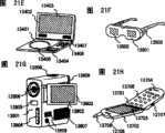
图21A示出了显示器,包含外壳13001、支撑底座13002、显示部分13003、扬声器部分13004、视频输入端13005等.具有应用了本发明的显示部分13003的该显示器,可以抑制由于环境温度变化所致亮度变化,由此可以减小表观亮度衰减.注意,该显示器包括用于信息显示的所有显示装置,例如用于个人计算机、TV广播接收机、广告显示器等的显示器.Fig. 21A shows a display including a casing 13001, a supporting
图21B示出了照相机,包含主体13101、显示部分13102、图像接收部分13103、操作键13104、外部连接端口13105、快门13106等.具有应用了本发明的显示部分13102的该照相机可以抑制由于环境温度变化所致亮度变化,由此可以减小表观亮度衰减.21B shows a camera including a
图21C示出了计算机,包含主体13201、外壳13202、显示部分13203、键盘13204、外部连接端口13205、指点鼠标13206等.具有应用了本发明的显示部分13203的该计算机可以抑制由于环境温度变化所致亮度变化,由此可以减小表观亮度衰减.21C shows a computer, including a
图21D示出了移动计算机,包含主体13301、显示部分13302、开关13303、操作键13304、IR端口13305等.具有应用了本发明的显示部分13302的该移动计算机可以抑制由于环境温度变化所致亮度变化,由此可以减小表观亮度衰减.Fig. 21D shows a mobile computer including a
图21E示出了设有记录介质的便携图像再现装置(特别地指DVD再现装置),其包含主体13401、外壳13402、显示部分A 13403、显示部分B 13404、记录介质(DVD)读取部分13405、操作键13406、扬声器部分13407等.显示部分A 13403主要显示图像数据,而显示部分B 13404主要显示文字数据.具有应用了本发明的显示部分A13403和B 13404的该图像再现装置可以抑制由于环境温度变化所致亮度变化,由此可以减小表观亮度衰减.Figure 21E shows a portable image reproducing device (in particular, a DVD reproducing device) provided with a recording medium, which includes a
图21F示出了护目镜型显示器(头戴式显示器),其包括主体13501、显示部分13502、臂部分13503等.具有应用了本发明的显示部分13502的该护目镜型显示器可以抑制由于环境温度变化所致亮度变化,由此可以减小表观亮度衰减.Fig. 21F shows a goggle-type display (head-mounted display), which includes a
图21G示出了摄像机,其包含主体13601、显示部分13602、外壳13603、外部连接端口13604、遥控器接收部分13605、图像接收部分13606、电池13607、音频输入部分13608、操作键13609、目镜部分13610等.具有应用了本发明的显示部分13602的该摄像机可以抑制由于环境温度变化所致亮度变化,由此可以减小表观亮度衰减.FIG. 21G shows a video camera, which includes a
图21H示出了便携电话,其包含主体13701、外壳13702、显示部分13703、音频输入部分13704、音频输出部分13705、操作键13706、外部连接端口13707、天线13708等.具有应用了本发明的显示部分13703的该便携电话可以抑制由于环境温度变化所致亮度变化,由此可以减小表观亮度衰减.FIG. 21H shows a cellular phone including a
如前所述,本发明可以应用于各种电子设备.As mentioned above, the present invention can be applied to various electronic devices.
Claims (19)
Translated fromChineseApplications Claiming Priority (2)
| Application Number | Priority Date | Filing Date | Title |
|---|---|---|---|
| JP2004224309 | 2004-07-30 | ||
| JP224309/2004 | 2004-07-30 |
Publications (2)
| Publication Number | Publication Date |
|---|---|
| CN101031947A CN101031947A (en) | 2007-09-05 |
| CN100485762Ctrue CN100485762C (en) | 2009-05-06 |
Family
ID=35786394
Family Applications (1)
| Application Number | Title | Priority Date | Filing Date |
|---|---|---|---|
| CNB2005800333865AExpired - Fee RelatedCN100485762C (en) | 2004-07-30 | 2005-07-28 | Display device, driving method of display device, and electronic apparatus |
Country Status (3)
| Country | Link |
|---|---|
| US (1) | US8154541B2 (en) |
| CN (1) | CN100485762C (en) |
| WO (1) | WO2006011666A1 (en) |
Families Citing this family (29)
| Publication number | Priority date | Publication date | Assignee | Title |
|---|---|---|---|---|
| US7442950B2 (en) | 2004-12-06 | 2008-10-28 | Semiconductor Energy Laboratory Co., Ltd. | Light emitting device |
| CN100538794C (en) | 2005-05-02 | 2009-09-09 | 株式会社半导体能源研究所 | Light emitting device, method of driving the same, display module, and electronic apparatus |
| US7986287B2 (en) | 2005-08-26 | 2011-07-26 | Semiconductor Energy Laboratory Co., Ltd. | Display device and method of driving the same |
| US7995012B2 (en) | 2005-12-27 | 2011-08-09 | Semiconductor Energy Laboratory Co., Ltd. | Light emitting device |
| EP1804229B1 (en) | 2005-12-28 | 2016-08-17 | Semiconductor Energy Laboratory Co., Ltd. | Display device and method for inspecting the same |
| FR2903224A1 (en)* | 2006-06-30 | 2008-01-04 | Thomson Licensing Sa | DISPLAY DEVICE AND USES THEREOF. |
| US7928939B2 (en)* | 2007-02-22 | 2011-04-19 | Apple Inc. | Display system |
| JP2009037221A (en)* | 2007-07-06 | 2009-02-19 | Semiconductor Energy Lab Co Ltd | LIGHT EMITTING DEVICE, ELECTRONIC DEVICE, AND LIGHT EMITTING DEVICE DRIVE METHOD |
| JP5301299B2 (en)* | 2008-01-31 | 2013-09-25 | 株式会社半導体エネルギー研究所 | Semiconductor device |
| JP4775408B2 (en)* | 2008-06-03 | 2011-09-21 | ソニー株式会社 | Display device, wiring layout method in display device, and electronic apparatus |
| US9370075B2 (en) | 2008-12-09 | 2016-06-14 | Ignis Innovation Inc. | System and method for fast compensation programming of pixels in a display |
| KR101750126B1 (en)* | 2010-01-20 | 2017-06-22 | 가부시키가이샤 한도오따이 에네루기 켄큐쇼 | Method for driving display device and liquid crystal display device |
| KR101744906B1 (en)* | 2010-01-20 | 2017-06-20 | 가부시키가이샤 한도오따이 에네루기 켄큐쇼 | Display device and method for driving the same |
| JP5422736B2 (en)* | 2010-04-13 | 2014-02-19 | 富士通株式会社 | Operation check test method, operation check test program, and clock distribution circuit |
| JP2012064570A (en) | 2010-08-20 | 2012-03-29 | Semiconductor Energy Lab Co Ltd | Illumination device |
| TWI440392B (en)* | 2011-03-09 | 2014-06-01 | Chunghwa Picture Tubes Ltd | Backlight module, over temperature protecting circuit and over temperature protecting method thereof |
| CN102169672B (en)* | 2011-03-19 | 2014-02-26 | 福州华映视讯有限公司 | Backlight module, over-temperature protective circuit and over-temperature protective method |
| US9935622B2 (en) | 2011-04-28 | 2018-04-03 | Semiconductor Energy Laboratory Co., Ltd. | Comparator and semiconductor device including comparator |
| CN107770462B (en)* | 2011-12-28 | 2020-09-22 | 株式会社尼康 | Imaging element and imaging device |
| US9183779B2 (en)* | 2012-02-23 | 2015-11-10 | Broadcom Corporation | AMOLED light sensing |
| JP6042187B2 (en)* | 2012-11-30 | 2016-12-14 | 株式会社ジャパンディスプレイ | OLED display device |
| US9245935B2 (en) | 2013-04-02 | 2016-01-26 | Semiconductor Energy Laboratory Co., Ltd. | Light-emitting device |
| JP6801943B2 (en)* | 2014-02-21 | 2020-12-16 | セイコーエプソン株式会社 | Organic electroluminescence equipment and electronic equipment |
| US10186512B2 (en)* | 2015-04-03 | 2019-01-22 | Sony Semiconductor Solutions Corporation | Solid-state image sensor, image capturing device, and electronic device |
| CN105007656B (en)* | 2015-07-14 | 2018-04-06 | 海宁海微电子科技有限公司 | The latch cicuit of multifunctional electric torch |
| CN105405864B (en)* | 2015-12-08 | 2019-05-17 | 昆山工研院新型平板显示技术中心有限公司 | The packaging method of display device and display device |
| US10854129B2 (en)* | 2018-06-18 | 2020-12-01 | Apple Inc. | Hybrid architecture for zero border display |
| CN116825030B (en)* | 2023-08-25 | 2023-11-10 | 惠科股份有限公司 | Driving control circuit of light emitting array, driving control method of driving control circuit and display screen |
| CN117219019B (en)* | 2023-09-07 | 2025-10-03 | 惠科股份有限公司 | Pixel driving circuit, display panel driving circuit, and display panel |
Citations (5)
| Publication number | Priority date | Publication date | Assignee | Title |
|---|---|---|---|---|
| EP1117085A2 (en)* | 2000-01-17 | 2001-07-18 | Sel Semiconductor Energy Laboratory Co., Ltd. | EL display system |
| JP2002123219A (en)* | 2000-08-10 | 2002-04-26 | Semiconductor Energy Lab Co Ltd | Display device and its driving method |
| JP2002333861A (en)* | 2000-04-18 | 2002-11-22 | Semiconductor Energy Lab Co Ltd | Display device |
| CN1409403A (en)* | 2001-09-28 | 2003-04-09 | 株式会社半导体能源研究所 | Light-emitting device and electronic equipment using said device |
| JP2003263132A (en)* | 2002-03-11 | 2003-09-19 | Matsushita Electric Ind Co Ltd | Display device |
Family Cites Families (18)
| Publication number | Priority date | Publication date | Assignee | Title |
|---|---|---|---|---|
| US6329758B1 (en)* | 1994-12-20 | 2001-12-11 | Unisplay S.A. | LED matrix display with intensity and color matching of the pixels |
| US20010030511A1 (en) | 2000-04-18 | 2001-10-18 | Shunpei Yamazaki | Display device |
| JP4841754B2 (en) | 2000-06-13 | 2011-12-21 | 株式会社半導体エネルギー研究所 | Active matrix light emitting device and electronic device |
| TW512304B (en) | 2000-06-13 | 2002-12-01 | Semiconductor Energy Lab | Display device |
| US6828950B2 (en)* | 2000-08-10 | 2004-12-07 | Semiconductor Energy Laboratory Co., Ltd. | Display device and method of driving the same |
| TW569016B (en)* | 2001-01-29 | 2004-01-01 | Semiconductor Energy Lab | Light emitting device |
| JP2003029710A (en) | 2001-07-19 | 2003-01-31 | Nippon Seiki Co Ltd | Drive circuit for organic electroluminescence element |
| JP2003202838A (en)* | 2001-10-31 | 2003-07-18 | Matsushita Electric Ind Co Ltd | Display device |
| US7023141B2 (en) | 2002-03-01 | 2006-04-04 | Semiconductor Energy Laboratory Co., Ltd. | Light emitting device and drive method thereof |
| JP4454943B2 (en) | 2002-03-01 | 2010-04-21 | 株式会社半導体エネルギー研究所 | Driving method of light emitting device |
| US20040150594A1 (en) | 2002-07-25 | 2004-08-05 | Semiconductor Energy Laboratory Co., Ltd. | Display device and drive method therefor |
| JP4447262B2 (en) | 2002-07-25 | 2010-04-07 | 株式会社半導体エネルギー研究所 | Display device, display device driving method, and electronic apparatus |
| JP2004205704A (en) | 2002-12-24 | 2004-07-22 | Toshiba Matsushita Display Technology Co Ltd | Organic el display |
| JP4205629B2 (en) | 2003-07-07 | 2009-01-07 | セイコーエプソン株式会社 | Digital / analog conversion circuit, electro-optical device and electronic apparatus |
| JP4781009B2 (en) | 2004-05-21 | 2011-09-28 | 株式会社半導体エネルギー研究所 | Display device and electronic device |
| US8421715B2 (en) | 2004-05-21 | 2013-04-16 | Semiconductor Energy Laboratory Co., Ltd. | Display device, driving method thereof and electronic appliance |
| JP4809658B2 (en) | 2004-10-29 | 2011-11-09 | 株式会社半導体エネルギー研究所 | Display device and electronic apparatus using the same |
| US9734901B2 (en) | 2004-10-29 | 2017-08-15 | Semiconductor Energy Laboratory Co., Ltd. | Display device with semiconductor memory cell |
- 2005
- 2005-07-28CNCNB2005800333865Apatent/CN100485762C/ennot_activeExpired - Fee Related
- 2005-07-28WOPCT/JP2005/014256patent/WO2006011666A1/enactiveApplication Filing
- 2005-07-28USUS11/572,158patent/US8154541B2/ennot_activeExpired - Fee Related
Patent Citations (5)
| Publication number | Priority date | Publication date | Assignee | Title |
|---|---|---|---|---|
| EP1117085A2 (en)* | 2000-01-17 | 2001-07-18 | Sel Semiconductor Energy Laboratory Co., Ltd. | EL display system |
| JP2002333861A (en)* | 2000-04-18 | 2002-11-22 | Semiconductor Energy Lab Co Ltd | Display device |
| JP2002123219A (en)* | 2000-08-10 | 2002-04-26 | Semiconductor Energy Lab Co Ltd | Display device and its driving method |
| CN1409403A (en)* | 2001-09-28 | 2003-04-09 | 株式会社半导体能源研究所 | Light-emitting device and electronic equipment using said device |
| JP2003263132A (en)* | 2002-03-11 | 2003-09-19 | Matsushita Electric Ind Co Ltd | Display device |
Also Published As
| Publication number | Publication date |
|---|---|
| US20080094009A1 (en) | 2008-04-24 |
| WO2006011666A1 (en) | 2006-02-02 |
| CN101031947A (en) | 2007-09-05 |
| US8154541B2 (en) | 2012-04-10 |
Similar Documents
| Publication | Publication Date | Title |
|---|---|---|
| CN100485762C (en) | Display device, driving method of display device, and electronic apparatus | |
| JP5288656B2 (en) | Light emitting device and driving method thereof | |
| US10998382B2 (en) | Self-light emitting display unit and electronic device | |
| CN100416865C (en) | display device | |
| CN1174356C (en) | Drive circuit and electronic device including organic electroluminescent element, and electro-optical device | |
| US8830218B2 (en) | Display device and electronic apparatus | |
| JP2002358048A (en) | Display device and its driving method | |
| CN115831047A (en) | A pixel circuit and its driving method, display substrate and display device | |
| USRE48891E1 (en) | Display apparatus and electronic apparatus | |
| CN100410988C (en) | Display device and driving method thereof | |
| CN112102775A (en) | Display device and brightness compensation method thereof | |
| US20230237949A1 (en) | Electronic device and driving method of electronic device | |
| JP4877872B2 (en) | Display device and active matrix display device | |
| JP2006091860A (en) | Display device, driving method of the same, and electronic device | |
| JP4539967B2 (en) | Luminescent panel drive device | |
| KR101383456B1 (en) | Organic Light Emitting Display | |
| KR101137710B1 (en) | Display device | |
| JP2008185671A (en) | Organic electroluminescence display device, control method for organic electroluminescence device, and electronic equipment | |
| JP2008191610A (en) | Organic el display device, method of controlling organic el display, and electronic equipment | |
| JP4823651B2 (en) | Light emitting device and manufacturing method thereof | |
| JP4849876B2 (en) | Display device |
Legal Events
| Date | Code | Title | Description |
|---|---|---|---|
| C06 | Publication | ||
| PB01 | Publication | ||
| C10 | Entry into substantive examination | ||
| SE01 | Entry into force of request for substantive examination | ||
| C14 | Grant of patent or utility model | ||
| GR01 | Patent grant | ||
| CF01 | Termination of patent right due to non-payment of annual fee | ||
| CF01 | Termination of patent right due to non-payment of annual fee | Granted publication date:20090506 Termination date:20180728 |