CN100481659C - Tunable semiconductor laser, method of manufacturing the same, and gas detector using the same - Google Patents
Tunable semiconductor laser, method of manufacturing the same, and gas detector using the sameDownload PDFInfo
- Publication number
- CN100481659C CN100481659CCNB2006800002566ACN200680000256ACN100481659CCN 100481659 CCN100481659 CCN 100481659CCN B2006800002566 ACNB2006800002566 ACN B2006800002566ACN 200680000256 ACN200680000256 ACN 200680000256ACN 100481659 CCN100481659 CCN 100481659C
- Authority
- CN
- China
- Prior art keywords
- diffraction grating
- semiconductor laser
- wavelength
- heating
- heating part
- Prior art date
- Legal status (The legal status is an assumption and is not a legal conclusion. Google has not performed a legal analysis and makes no representation as to the accuracy of the status listed.)
- Expired - Fee Related
Links
Images


Classifications
- H—ELECTRICITY
- H01—ELECTRIC ELEMENTS
- H01S—DEVICES USING THE PROCESS OF LIGHT AMPLIFICATION BY STIMULATED EMISSION OF RADIATION [LASER] TO AMPLIFY OR GENERATE LIGHT; DEVICES USING STIMULATED EMISSION OF ELECTROMAGNETIC RADIATION IN WAVE RANGES OTHER THAN OPTICAL
- H01S3/00—Lasers, i.e. devices using stimulated emission of electromagnetic radiation in the infrared, visible or ultraviolet wave range
- H01S3/10—Controlling the intensity, frequency, phase, polarisation or direction of the emitted radiation, e.g. switching, gating, modulating or demodulating
- H—ELECTRICITY
- H01—ELECTRIC ELEMENTS
- H01S—DEVICES USING THE PROCESS OF LIGHT AMPLIFICATION BY STIMULATED EMISSION OF RADIATION [LASER] TO AMPLIFY OR GENERATE LIGHT; DEVICES USING STIMULATED EMISSION OF ELECTROMAGNETIC RADIATION IN WAVE RANGES OTHER THAN OPTICAL
- H01S5/00—Semiconductor lasers
- H01S5/06—Arrangements for controlling the laser output parameters, e.g. by operating on the active medium
- H01S5/062—Arrangements for controlling the laser output parameters, e.g. by operating on the active medium by varying the potential of the electrodes
- H01S5/0625—Arrangements for controlling the laser output parameters, e.g. by operating on the active medium by varying the potential of the electrodes in multi-section lasers
- H01S5/06255—Controlling the frequency of the radiation
- H01S5/06256—Controlling the frequency of the radiation with DBR-structure
- G—PHYSICS
- G01—MEASURING; TESTING
- G01J—MEASUREMENT OF INTENSITY, VELOCITY, SPECTRAL CONTENT, POLARISATION, PHASE OR PULSE CHARACTERISTICS OF INFRARED, VISIBLE OR ULTRAVIOLET LIGHT; COLORIMETRY; RADIATION PYROMETRY
- G01J3/00—Spectrometry; Spectrophotometry; Monochromators; Measuring colours
- G01J3/02—Details
- G01J3/10—Arrangements of light sources specially adapted for spectrometry or colorimetry
- G—PHYSICS
- G01—MEASURING; TESTING
- G01J—MEASUREMENT OF INTENSITY, VELOCITY, SPECTRAL CONTENT, POLARISATION, PHASE OR PULSE CHARACTERISTICS OF INFRARED, VISIBLE OR ULTRAVIOLET LIGHT; COLORIMETRY; RADIATION PYROMETRY
- G01J3/00—Spectrometry; Spectrophotometry; Monochromators; Measuring colours
- G01J3/28—Investigating the spectrum
- G01J3/42—Absorption spectrometry; Double beam spectrometry; Flicker spectrometry; Reflection spectrometry
- G—PHYSICS
- G01—MEASURING; TESTING
- G01N—INVESTIGATING OR ANALYSING MATERIALS BY DETERMINING THEIR CHEMICAL OR PHYSICAL PROPERTIES
- G01N21/00—Investigating or analysing materials by the use of optical means, i.e. using sub-millimetre waves, infrared, visible or ultraviolet light
- G01N21/17—Systems in which incident light is modified in accordance with the properties of the material investigated
- G01N21/25—Colour; Spectral properties, i.e. comparison of effect of material on the light at two or more different wavelengths or wavelength bands
- G01N21/31—Investigating relative effect of material at wavelengths characteristic of specific elements or molecules, e.g. atomic absorption spectrometry
- G01N21/39—Investigating relative effect of material at wavelengths characteristic of specific elements or molecules, e.g. atomic absorption spectrometry using tunable lasers
- H—ELECTRICITY
- H01—ELECTRIC ELEMENTS
- H01S—DEVICES USING THE PROCESS OF LIGHT AMPLIFICATION BY STIMULATED EMISSION OF RADIATION [LASER] TO AMPLIFY OR GENERATE LIGHT; DEVICES USING STIMULATED EMISSION OF ELECTROMAGNETIC RADIATION IN WAVE RANGES OTHER THAN OPTICAL
- H01S5/00—Semiconductor lasers
- H01S5/06—Arrangements for controlling the laser output parameters, e.g. by operating on the active medium
- H01S5/0607—Arrangements for controlling the laser output parameters, e.g. by operating on the active medium by varying physical parameters other than the potential of the electrodes, e.g. by an electric or magnetic field, mechanical deformation, pressure, light, temperature
- H01S5/0612—Arrangements for controlling the laser output parameters, e.g. by operating on the active medium by varying physical parameters other than the potential of the electrodes, e.g. by an electric or magnetic field, mechanical deformation, pressure, light, temperature controlled by temperature
- H—ELECTRICITY
- H01—ELECTRIC ELEMENTS
- H01S—DEVICES USING THE PROCESS OF LIGHT AMPLIFICATION BY STIMULATED EMISSION OF RADIATION [LASER] TO AMPLIFY OR GENERATE LIGHT; DEVICES USING STIMULATED EMISSION OF ELECTROMAGNETIC RADIATION IN WAVE RANGES OTHER THAN OPTICAL
- H01S5/00—Semiconductor lasers
- H01S5/06—Arrangements for controlling the laser output parameters, e.g. by operating on the active medium
- H01S5/062—Arrangements for controlling the laser output parameters, e.g. by operating on the active medium by varying the potential of the electrodes
- H01S5/0625—Arrangements for controlling the laser output parameters, e.g. by operating on the active medium by varying the potential of the electrodes in multi-section lasers
- H01S5/06255—Controlling the frequency of the radiation
- H01S5/06258—Controlling the frequency of the radiation with DFB-structure
- G—PHYSICS
- G01—MEASURING; TESTING
- G01J—MEASUREMENT OF INTENSITY, VELOCITY, SPECTRAL CONTENT, POLARISATION, PHASE OR PULSE CHARACTERISTICS OF INFRARED, VISIBLE OR ULTRAVIOLET LIGHT; COLORIMETRY; RADIATION PYROMETRY
- G01J3/00—Spectrometry; Spectrophotometry; Monochromators; Measuring colours
- G01J3/02—Details
- G01J3/027—Control of working procedures of a spectrometer; Failure detection; Bandwidth calculation
- G—PHYSICS
- G01—MEASURING; TESTING
- G01N—INVESTIGATING OR ANALYSING MATERIALS BY DETERMINING THEIR CHEMICAL OR PHYSICAL PROPERTIES
- G01N21/00—Investigating or analysing materials by the use of optical means, i.e. using sub-millimetre waves, infrared, visible or ultraviolet light
- G01N21/17—Systems in which incident light is modified in accordance with the properties of the material investigated
- G01N21/25—Colour; Spectral properties, i.e. comparison of effect of material on the light at two or more different wavelengths or wavelength bands
- G01N21/31—Investigating relative effect of material at wavelengths characteristic of specific elements or molecules, e.g. atomic absorption spectrometry
- G01N21/39—Investigating relative effect of material at wavelengths characteristic of specific elements or molecules, e.g. atomic absorption spectrometry using tunable lasers
- G01N2021/396—Type of laser source
- G01N2021/399—Diode laser
- H—ELECTRICITY
- H01—ELECTRIC ELEMENTS
- H01L—SEMICONDUCTOR DEVICES NOT COVERED BY CLASS H10
- H01L2224/00—Indexing scheme for arrangements for connecting or disconnecting semiconductor or solid-state bodies and methods related thereto as covered by H01L24/00
- H01L2224/01—Means for bonding being attached to, or being formed on, the surface to be connected, e.g. chip-to-package, die-attach, "first-level" interconnects; Manufacturing methods related thereto
- H01L2224/42—Wire connectors; Manufacturing methods related thereto
- H01L2224/47—Structure, shape, material or disposition of the wire connectors after the connecting process
- H01L2224/48—Structure, shape, material or disposition of the wire connectors after the connecting process of an individual wire connector
- H01L2224/4805—Shape
- H01L2224/4809—Loop shape
- H01L2224/48091—Arched
- H—ELECTRICITY
- H01—ELECTRIC ELEMENTS
- H01S—DEVICES USING THE PROCESS OF LIGHT AMPLIFICATION BY STIMULATED EMISSION OF RADIATION [LASER] TO AMPLIFY OR GENERATE LIGHT; DEVICES USING STIMULATED EMISSION OF ELECTROMAGNETIC RADIATION IN WAVE RANGES OTHER THAN OPTICAL
- H01S5/00—Semiconductor lasers
- H01S5/02—Structural details or components not essential to laser action
- H01S5/022—Mountings; Housings
- H01S5/02208—Mountings; Housings characterised by the shape of the housings
- H—ELECTRICITY
- H01—ELECTRIC ELEMENTS
- H01S—DEVICES USING THE PROCESS OF LIGHT AMPLIFICATION BY STIMULATED EMISSION OF RADIATION [LASER] TO AMPLIFY OR GENERATE LIGHT; DEVICES USING STIMULATED EMISSION OF ELECTROMAGNETIC RADIATION IN WAVE RANGES OTHER THAN OPTICAL
- H01S5/00—Semiconductor lasers
- H01S5/02—Structural details or components not essential to laser action
- H01S5/022—Mountings; Housings
- H01S5/023—Mount members, e.g. sub-mount members
- H01S5/02325—Mechanically integrated components on mount members or optical micro-benches
- H—ELECTRICITY
- H01—ELECTRIC ELEMENTS
- H01S—DEVICES USING THE PROCESS OF LIGHT AMPLIFICATION BY STIMULATED EMISSION OF RADIATION [LASER] TO AMPLIFY OR GENERATE LIGHT; DEVICES USING STIMULATED EMISSION OF ELECTROMAGNETIC RADIATION IN WAVE RANGES OTHER THAN OPTICAL
- H01S5/00—Semiconductor lasers
- H01S5/02—Structural details or components not essential to laser action
- H01S5/022—Mountings; Housings
- H01S5/0233—Mounting configuration of laser chips
- H01S5/02345—Wire-bonding
- H—ELECTRICITY
- H01—ELECTRIC ELEMENTS
- H01S—DEVICES USING THE PROCESS OF LIGHT AMPLIFICATION BY STIMULATED EMISSION OF RADIATION [LASER] TO AMPLIFY OR GENERATE LIGHT; DEVICES USING STIMULATED EMISSION OF ELECTROMAGNETIC RADIATION IN WAVE RANGES OTHER THAN OPTICAL
- H01S5/00—Semiconductor lasers
- H01S5/02—Structural details or components not essential to laser action
- H01S5/024—Arrangements for thermal management
- H01S5/02407—Active cooling, e.g. the laser temperature is controlled by a thermo-electric cooler or water cooling
- H01S5/02415—Active cooling, e.g. the laser temperature is controlled by a thermo-electric cooler or water cooling by using a thermo-electric cooler [TEC], e.g. Peltier element
- H—ELECTRICITY
- H01—ELECTRIC ELEMENTS
- H01S—DEVICES USING THE PROCESS OF LIGHT AMPLIFICATION BY STIMULATED EMISSION OF RADIATION [LASER] TO AMPLIFY OR GENERATE LIGHT; DEVICES USING STIMULATED EMISSION OF ELECTROMAGNETIC RADIATION IN WAVE RANGES OTHER THAN OPTICAL
- H01S5/00—Semiconductor lasers
- H01S5/02—Structural details or components not essential to laser action
- H01S5/024—Arrangements for thermal management
- H01S5/02438—Characterized by cooling of elements other than the laser chip, e.g. an optical element being part of an external cavity or a collimating lens
- H—ELECTRICITY
- H01—ELECTRIC ELEMENTS
- H01S—DEVICES USING THE PROCESS OF LIGHT AMPLIFICATION BY STIMULATED EMISSION OF RADIATION [LASER] TO AMPLIFY OR GENERATE LIGHT; DEVICES USING STIMULATED EMISSION OF ELECTROMAGNETIC RADIATION IN WAVE RANGES OTHER THAN OPTICAL
- H01S5/00—Semiconductor lasers
- H01S5/02—Structural details or components not essential to laser action
- H01S5/026—Monolithically integrated components, e.g. waveguides, monitoring photo-detectors, drivers
- H—ELECTRICITY
- H01—ELECTRIC ELEMENTS
- H01S—DEVICES USING THE PROCESS OF LIGHT AMPLIFICATION BY STIMULATED EMISSION OF RADIATION [LASER] TO AMPLIFY OR GENERATE LIGHT; DEVICES USING STIMULATED EMISSION OF ELECTROMAGNETIC RADIATION IN WAVE RANGES OTHER THAN OPTICAL
- H01S5/00—Semiconductor lasers
- H01S5/04—Processes or apparatus for excitation, e.g. pumping, e.g. by electron beams
- H01S5/042—Electrical excitation ; Circuits therefor
- H01S5/0425—Electrodes, e.g. characterised by the structure
- H01S5/04256—Electrodes, e.g. characterised by the structure characterised by the configuration
- H—ELECTRICITY
- H01—ELECTRIC ELEMENTS
- H01S—DEVICES USING THE PROCESS OF LIGHT AMPLIFICATION BY STIMULATED EMISSION OF RADIATION [LASER] TO AMPLIFY OR GENERATE LIGHT; DEVICES USING STIMULATED EMISSION OF ELECTROMAGNETIC RADIATION IN WAVE RANGES OTHER THAN OPTICAL
- H01S5/00—Semiconductor lasers
- H01S5/10—Construction or shape of the optical resonator, e.g. extended or external cavity, coupled cavities, bent-guide, varying width, thickness or composition of the active region
- H01S5/12—Construction or shape of the optical resonator, e.g. extended or external cavity, coupled cavities, bent-guide, varying width, thickness or composition of the active region the resonator having a periodic structure, e.g. in distributed feedback [DFB] lasers
- H01S5/1203—Construction or shape of the optical resonator, e.g. extended or external cavity, coupled cavities, bent-guide, varying width, thickness or composition of the active region the resonator having a periodic structure, e.g. in distributed feedback [DFB] lasers over only a part of the length of the active region
- H—ELECTRICITY
- H01—ELECTRIC ELEMENTS
- H01S—DEVICES USING THE PROCESS OF LIGHT AMPLIFICATION BY STIMULATED EMISSION OF RADIATION [LASER] TO AMPLIFY OR GENERATE LIGHT; DEVICES USING STIMULATED EMISSION OF ELECTROMAGNETIC RADIATION IN WAVE RANGES OTHER THAN OPTICAL
- H01S5/00—Semiconductor lasers
- H01S5/20—Structure or shape of the semiconductor body to guide the optical wave ; Confining structures perpendicular to the optical axis, e.g. index or gain guiding, stripe geometry, broad area lasers, gain tailoring, transverse or lateral reflectors, special cladding structures, MQW barrier reflection layers
- H01S5/22—Structure or shape of the semiconductor body to guide the optical wave ; Confining structures perpendicular to the optical axis, e.g. index or gain guiding, stripe geometry, broad area lasers, gain tailoring, transverse or lateral reflectors, special cladding structures, MQW barrier reflection layers having a ridge or stripe structure
- H01S5/223—Buried stripe structure
- H01S5/2231—Buried stripe structure with inner confining structure only between the active layer and the upper electrode
- H—ELECTRICITY
- H01—ELECTRIC ELEMENTS
- H01S—DEVICES USING THE PROCESS OF LIGHT AMPLIFICATION BY STIMULATED EMISSION OF RADIATION [LASER] TO AMPLIFY OR GENERATE LIGHT; DEVICES USING STIMULATED EMISSION OF ELECTROMAGNETIC RADIATION IN WAVE RANGES OTHER THAN OPTICAL
- H01S5/00—Semiconductor lasers
- H01S5/20—Structure or shape of the semiconductor body to guide the optical wave ; Confining structures perpendicular to the optical axis, e.g. index or gain guiding, stripe geometry, broad area lasers, gain tailoring, transverse or lateral reflectors, special cladding structures, MQW barrier reflection layers
- H01S5/22—Structure or shape of the semiconductor body to guide the optical wave ; Confining structures perpendicular to the optical axis, e.g. index or gain guiding, stripe geometry, broad area lasers, gain tailoring, transverse or lateral reflectors, special cladding structures, MQW barrier reflection layers having a ridge or stripe structure
- H01S5/227—Buried mesa structure ; Striped active layer
Landscapes
- Physics & Mathematics (AREA)
- Spectroscopy & Molecular Physics (AREA)
- General Physics & Mathematics (AREA)
- Optics & Photonics (AREA)
- Electromagnetism (AREA)
- Condensed Matter Physics & Semiconductors (AREA)
- Chemical & Material Sciences (AREA)
- Life Sciences & Earth Sciences (AREA)
- Health & Medical Sciences (AREA)
- Analytical Chemistry (AREA)
- Biochemistry (AREA)
- General Health & Medical Sciences (AREA)
- Immunology (AREA)
- Pathology (AREA)
- Engineering & Computer Science (AREA)
- Plasma & Fusion (AREA)
- Semiconductor Lasers (AREA)
Abstract
Description
Translated fromChinese技术领域technical field
本发明涉及可调半导体激光器、其制造方法、以及使用该激光器的气体检测器。更特别地,本发明涉及能够输出激光束并控制波长的简单配置的可调激光器、其制造方法、以及使用该激光器的气体检测器。The present invention relates to a tunable semiconductor laser, a manufacturing method thereof, and a gas detector using the laser. More particularly, the present invention relates to a simple configuration tunable laser capable of outputting a laser beam and controlling a wavelength, a manufacturing method thereof, and a gas detector using the same.
背景技术Background technique
常规地,已知有利用TDLAS(可调二极管激光吸收光谱)方案类型的气体检测器,其中与检测目标气体(例如甲烷气体或乙醇气体)的吸收线波长匹配的激光束通过利用气体特有的吸收线辐射到检测空间中。然后,检测气体的存在与否、浓度等通过测量辐射激光束的衰减状态来检测。Conventionally, there is known a gas detector utilizing a TDLAS (Tunable Diode Laser Absorption Spectroscopy) scheme type in which a laser beam matching the wavelength of an absorption line of a detection target gas (such as methane gas or ethanol gas) is obtained by utilizing the gas-specific absorption The line radiates into the detection space. Then, the presence or absence, concentration, etc. of the detection gas are detected by measuring the attenuation state of the irradiated laser beam.
作为用于上述类型气体检测器的半导体激光器,已知有可调半导体激光器,例如后述专利文献1中公开的DFB(分布式反馈)激光器和述专利文献2中公开的DBR(分布式布拉格反射器)激光器。As semiconductor lasers used in the above-mentioned type of gas detectors, tunable semiconductor lasers are known, such as DFB (Distributed Feedback) lasers disclosed in
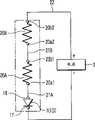
如图9所示,例如,专利文献1公开的DFB激光器构成如下:有源层51和InP层52形成在n-InP衬底53的一个表面上,n型电极54形成在n-InP衬底53的相反表面上。As shown in FIG. 9, for example, the DFB laser disclosed in
包括窗口的SiO2绝缘膜55和形成为含有Au以用于驱动电流注入的p型电极56形成在有源层51上方。A SiO2
此外,用于电阻膜58的电极59a和59b分别以岛状形成在p型电极56的右手区域中。Further, electrodes 59 a and 59 b for the resistance film 58 are formed in an island shape in the right-hand region of the p-
此外,包括SiO2绝缘膜57和Pt的电阻膜58形成在有源层51上方。In addition, a resistance film 58 including a SiO2 insulating film 57 and Pt is formed over the
在这种情况下,电阻膜58的两端形成为接触预先形成的电极59a和59b。In this case, both ends of the resistance film 58 are formed in contact with previously formed electrodes 59a and 59b.
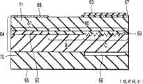
如图10A和10B所示,专利文献2中公开的DBR激光器包括半导体光学器件64和热沉65,其中半导体光学器件64包括光波导62和通过绝缘膜67形成以加热光波导62的至少一部分的加热部分63;热沉65形成来安装半导体光学器件64,直接接触光波导62的一部分,且通过空隙部分66接触光波导62的其他部分。As shown in FIGS. 10A and 10B , the DBR laser disclosed in
此外,将衬底70周期性蚀刻,并由此将波纹状衍射光栅69形成在光波导62的除有源区61之外的区域80中。In addition, the
根据DBR激光器,在除有源区61之外的区域中,形成衍射光栅69的部分称作DBR区域C,且其余部分称作相位控制区域B。According to the DBR laser, in a region other than the
如图10B所示,用作非辐射区域80的InGaAsP波导层、和InP盖层71形成在有源区61的外围部分。As shown in FIG. 10B , an InGaAsP waveguide layer serving as the
N型电极68通过进行例如Au和Ge的气相沉积经由InP盖层71形成在有源区61的上表面上。N-
P型电极(未示出)通过进行例如Au和Zn的气相沉积形成在衬底70的底表面上。A P-type electrode (not shown) is formed on the bottom surface of the
例如,具有不同于上述专利文献1中公开的DFB激光器构造的DFB激光器有后述专利文献3中公开的局部衍射光栅半导体激光器(PC-LD)和具有两个衍射光栅的分布式反馈半导体激光器,其为后述专利文献4中公开的激光器。For example, DFB lasers having a structure different from the DFB laser disclosed in
专利文献1:日本专利申请特开No.4-72783Patent Document 1: Japanese Patent Application Laid-Open No. 4-72783
专利文献2:日本专利申请特开No.9-74250Patent Document 2: Japanese Patent Application Laid-Open No. 9-74250
专利文献3:日本专利申请特开No.6-310806Patent Document 3: Japanese Patent Application Laid-Open No. 6-310806
专利文献4:日本专利申请特开No.2004-31827Patent Document 4: Japanese Patent Application Laid-Open No. 2004-31827
发明内容Contents of the invention
在上述可调半导体激光器用作气体检测器光源由此通过利用TDLAS方案检测检测空间中的检测目标气体的情况下,进行如下操作。调节半导体激光器,锁定辐射束的波长到检测目标气体特有的吸收线,锁定波长的激光束向检测空间辐射,并接收与激光束的辐射相关的来自检测空间的反射光。In the case where the above-described tunable semiconductor laser is used as a light source for a gas detector to thereby detect a detection target gas in a detection space by utilizing the TDLAS scheme, the following operations are performed. Adjust the semiconductor laser, lock the wavelength of the radiation beam to the specific absorption line of the detection target gas, radiate the locked wavelength laser beam to the detection space, and receive the reflected light from the detection space related to the radiation of the laser beam.
在这种情况下,半导体激光器的特征在于,辐射束的波长根据光波导的折射率来确定,且光波导的折射率根据温度或载流子密度(注入电流)来确定。In this case, the semiconductor laser is characterized in that the wavelength of the radiation beam is determined according to the refractive index of the optical waveguide, and the refractive index of the optical waveguide is determined according to the temperature or carrier density (injection current).
其他特征在于,在温度改变的情况下,虽然在激光束被调节从而被锁定到检测目标气体特有的吸收线时的响应速度低,但折射率的变化范围增大,以致于可以设置大的可调波长范围。Other features are that in the case of a temperature change, although the response speed is low when the laser beam is adjusted so as to be locked to the absorption line peculiar to the detection target gas, the range of change in the refractive index is increased so that a large adjustable range can be set. Tuning wavelength range.
另一方面,特征在于,在载流子密度改变的情况下,虽然在激光束被调节从而锁定到检测目标气体特有的吸收线时的响应速度高,但折射率在载流子密度的某一水平饱和,以致于变化范围窄,且因此可调波长范围不能设置得很大。On the other hand, it is characterized in that, in the case where the carrier density is changed, although the response speed when the laser beam is adjusted so as to be locked to the absorption line peculiar to the detection target gas is high, the refractive index is at a certain level of the carrier density. The level is saturated so that the variation range is narrow, and thus the adjustable wavelength range cannot be set very large.
在具有上述特征的半导体激光器被调节从而将辐照束的波长锁定到检测目标气体特有的吸收线的情况下,检测目标气体的吸收线波长和包括吸收线波长中心的范围是不同的。因此,使激光束的波长可调,以便能够有与检测目标气体的类型相应的足够的波长可调波长范围。In the case where the semiconductor laser having the above characteristics is adjusted to lock the wavelength of the irradiated beam to the absorption line specific to the detection target gas, the absorption line wavelength of the detection target gas and the range including the center of the absorption line wavelength are different. Therefore, the wavelength of the laser beam is made tunable so that there can be a sufficient wavelength tunable wavelength range corresponding to the type of detection target gas.
然而,已知,在根据上述类型的TDLAS方案的气体检测器中,只要气体具有约10KHz的调制频率,那么任何类型的检测目标气体都是充分可寻的。因此,即使当越过响应速度优先设置折射率变化大小时,仅通过改变温度就足以追踪气体。However, it is known that any type of detection target gas is sufficiently seekable as long as the gas has a modulation frequency of about 10 KHz in a gas detector according to the above-mentioned type of TDLAS scheme. Therefore, even when the magnitude of the refractive index change is prioritized over the response speed, it is sufficient to track the gas simply by changing the temperature.
后述的专利文献5公开了一种便携式气体浓度测量装置,其被小型化以便于使用并能够容易地检测例如气体的浓度和存在与否。然而,在这种便携式气体浓度测量装置的情况下,外壳中的部件安装空间是有限的,由于装置采用电池驱动,因此必须限制功耗,并且仅能在外壳中提供单个电源。
专利文献5:日本专利申请特开No.2005-106521Patent Document 5: Japanese Patent Application Laid-Open No. 2005-106521
因此,作为用于上述类型的这种便携式气体浓度测量装置的半导体激光器,需要能够利用单个电源输出激光并调节波长,且同时能够获得足够的可调波长范围的半导体激光器。Therefore, as a semiconductor laser used in such a portable gas concentration measuring device of the above-mentioned type, a semiconductor laser capable of outputting laser light and adjusting the wavelength with a single power source while obtaining a sufficient adjustable wavelength range is required.
然而,在如上述专利文献1和专利文献2中公开的半导体激光器中,虽然激光输出和波长可以彼此独立控制,但加热电源和激光驱动电源单独配置。在这种情况下,问题在于不仅结构复杂,而且该结构不能适用于例如其中仅单个电源能设置在外壳中的便携式气体浓度测量装置。However, in the semiconductor lasers disclosed in
为了解决上述常规技术的问题,本发明的目的在于,提供一种可调半导体激光器、其制造方法、以及使用该激光器的气体检测器,其中,采用简单配置,在通过TDLAS方案检测气体的情况下,半导体激光器能够在足够的可调波长范围内通过单路电流控制波长和激光输出,且因此能够实现公用单个电源用于加热电源和激光器驱动电源。因此,降低了实际安装中所需的安装空间。In order to solve the problems of the above-mentioned conventional techniques, an object of the present invention is to provide a tunable semiconductor laser, its manufacturing method, and a gas detector using the same, wherein, with a simple configuration, in the case of detecting gas by the TDLAS scheme , the semiconductor laser can control the wavelength and laser output through a single current within a sufficient adjustable wavelength range, and therefore can realize a common single power supply for heating power and laser driving power. Therefore, the installation space required in actual installation is reduced.
为了实现上述目的,根据本发明的第一方面,提供一种可调半导体激光器,包括:半导体衬底(10);形成在该半导体衬底上方并产生光的有源层(12);波长控制区域(D),该波长控制区域形成为包括该有源层,形成在光波导中且在至少一部分中包括衍射光栅(14),该光波导引导该有源层产生的光,该衍射光栅(14)从该有源层产生的光选择具有预定波长的光;形成在该光波导上方的盖层(cladding layer)(13);形成在该盖层上方的绝缘膜(19);形成在该半导体衬底下面的第一驱动电极(17);形成在该盖层上方的第二驱动电极(18);形成在该绝缘膜上方并用于加热该波长控制区域的至少一部分的加热部分(20);设置在该加热部分(20)中的第一加热端子(20a)和第二加热端子(20b);连接在该第二驱动电极和该第一加热端子之间的第一连接线(21);以及通过电源连接在该第一驱动电极和该第二加热端子之间的第二连接线(22),其中调节从该电源提供到通过该加热部分串联连接的该第一和第二连接线的电流,由此可以控制从该光波导传送到外部的光的波长。In order to achieve the above object, according to the first aspect of the present invention, a tunable semiconductor laser is provided, comprising: a semiconductor substrate (10); an active layer (12) formed on the semiconductor substrate and generating light; wavelength control A region (D), the wavelength control region formed to include the active layer, is formed in an optical waveguide that guides light generated by the active layer and includes a diffraction grating (14) in at least a portion, the diffraction grating ( 14) Select light having a predetermined wavelength from the light generated from the active layer; a cladding layer (13) formed over the optical waveguide; an insulating film (19) formed over the cladding layer; A first driving electrode (17) under the semiconductor substrate; a second driving electrode (18) formed over the capping layer; a heating portion (20) formed over the insulating film and for heating at least a part of the wavelength control region ; a first heating terminal ( 20 a ) and a second heating terminal ( 20 b ) arranged in the heating portion ( 20 ); a first connection line ( 21 ) connected between the second driving electrode and the first heating terminal and a second connection line (22) connected between the first drive electrode and the second heating terminal through a power supply, wherein regulation is provided from the power supply to the first and second connection lines connected in series through the heating portion The current can control the wavelength of light transmitted from the optical waveguide to the outside.
此外,根据本发明的第二方面,提供一种根据第一方面的可调半导体激光器,其中:该波长控制区域包括由衍射光栅形成的分布式布拉格反射区(C)和邻接该分布式布拉格反射区的相位调节区(B);且该加热部分构造为能够加热该相位调节区的至少一部分。Furthermore, according to a second aspect of the present invention, there is provided a tunable semiconductor laser according to the first aspect, wherein: the wavelength control region includes a distributed Bragg reflection region (C) formed by a diffraction grating and adjacent to the distributed Bragg reflection A phase adjustment zone (B) of the zone; and the heating portion is configured to be capable of heating at least a portion of the phase adjustment zone.
此外,根据本发明的第三方面,提供一种根据第二方面的可调半导体激光器,其中该加热部分进一步构造为能够均匀加热该分布式布拉格反射区的整个区域。Furthermore, according to a third aspect of the present invention, there is provided a tunable semiconductor laser according to the second aspect, wherein the heating portion is further configured to be able to uniformly heat the entire area of the distributed Bragg reflection region.
此外,根据本发明的第四方面,提供一种根据第一方面的可调半导体激光器,其中:该波长控制区包括一衍射光栅;且该加热部分构造为能够均匀加热所述一衍射光栅的整个区域。Furthermore, according to a fourth aspect of the present invention, there is provided a tunable semiconductor laser according to the first aspect, wherein: the wavelength control region includes a diffraction grating; and the heating portion is configured to uniformly heat the entirety of the diffraction grating area.
此外,根据本发明的第五方面,提供一种根据第四方面的可调半导体激光器,其中所述一衍射光栅跨该光波导的整个区域形成。Furthermore, according to a fifth aspect of the present invention, there is provided the tunable semiconductor laser according to the fourth aspect, wherein said one diffraction grating is formed across the entire area of the optical waveguide.
此外,根据本发明的第六方面,提供一种根据第四方面的可调半导体激光器,其中所述一衍射光栅形成在该光波导的一部分中。Furthermore, according to a sixth aspect of the present invention, there is provided the tunable semiconductor laser according to the fourth aspect, wherein said one diffraction grating is formed in a part of the optical waveguide.
此外,根据本发明的第七方面,提供一种根据第一方面的可调半导体激光器,其中:该波长控制区域由形成在该光波导的多个部分中的多个衍射光栅(14a、14b)构成;且该加热部分构造为能够加热该多个衍射光栅,使得各个该多个衍射光栅选择的各波长彼此相同。Furthermore, according to a seventh aspect of the present invention, there is provided a tunable semiconductor laser according to the first aspect, wherein: the wavelength control region is formed by a plurality of diffraction gratings (14a, 14b) formed in parts of the optical waveguide and the heating portion is configured to be capable of heating the plurality of diffraction gratings so that the wavelengths selected by each of the plurality of diffraction gratings are the same as each other.
此外,根据本发明的第八方面,提供一种根据第七方面的可调半导体激光器,其中该加热部分由分别加热该多个衍射光栅的多个加热部分构成,且该多个加热部分串联连接。Furthermore, according to an eighth aspect of the present invention, there is provided a tunable semiconductor laser according to the seventh aspect, wherein the heating section is composed of a plurality of heating sections respectively heating the plurality of diffraction gratings, and the plurality of heating sections are connected in series .
此外,根据本发明的第九方面,提供一种根据第一方面的可调半导体激光器,其中该加热部分由薄膜电阻器构成。Furthermore, according to a ninth aspect of the present invention, there is provided the tunable semiconductor laser according to the first aspect, wherein the heating portion is constituted by a thin film resistor.
此外,根据本发明的第十方面,提供一种根据第一方面的可调半导体激光器,其用在气体检测器中,该气体检测器辐射具有预定波长的激光束到检测空间中,并利用检测目标气体削弱激光束的特性通过使用可调二极管激光吸收谱方案进行气体检测。Furthermore, according to a tenth aspect of the present invention, there is provided the tunable semiconductor laser according to the first aspect, which is used in a gas detector that radiates a laser beam having a predetermined wavelength into a detection space, and uses the detection The properties of the target gas attenuate the laser beam by using a tunable diode laser absorption spectroscopy scheme for gas detection.
此外,为了实现上述目的,根据本发明的第十一方面,提供一种包括可调半导体激光器的气体检测器,其将具有预定波长的激光束辐射到检测空间中,并利用检测目标气体削弱激光束的特性通过使用可调二极管激光吸收谱方案进行气体检测,其中该可调半导体激光器包括:半导体衬底(10);形成在该半导体衬底上方并产生光的有源层(12);波长控制区域(D),该波长控制区域形成为包括该有源层,形成在光波导中且在至少一部分中包括衍射光栅(14),该光波导引导该有源层产生的光,该衍射光栅(14)从该有源层产生的光选择具有预定波长的光;形成在该光波导上方的盖层(13);形成在该盖层上方的绝缘膜(19);形成在该半导体衬底下面的第一驱动电极(17);形成在该盖层上方的第二驱动电极(18);形成在该绝缘膜上方并用于加热该波长控制区域的至少一部分的加热部分(20);设置在该加热部分(20)中的第一加热端子(20a)和第二加热端子(20b);连接在该第二驱动电极和该第一加热端子之间的第一连接线(21);以及通过电源连接在该第一驱动电极和该第二加热端子之间的第二连接线(22),其中调节从该电源提供到通过该加热部分串联连接的该第一和第二连接线的电流,由此可以控制从该光波导传送到外部的光的波长。In addition, in order to achieve the above object, according to the eleventh aspect of the present invention, there is provided a gas detector including a tunable semiconductor laser, which radiates a laser beam with a predetermined wavelength into the detection space, and weakens the laser light by detecting the target gas. The characteristics of the beam are gas detection by using a tunable diode laser absorption spectrum scheme, wherein the tunable semiconductor laser comprises: a semiconductor substrate (10); an active layer (12) formed over the semiconductor substrate and generating light; wavelength a control region (D), the wavelength control region formed to include the active layer, formed in an optical waveguide that guides light generated by the active layer and including in at least a portion a diffraction grating (14), the diffraction grating (14) Select light having a predetermined wavelength from the light generated from the active layer; a cover layer (13) formed over the optical waveguide; an insulating film (19) formed over the cover layer; formed on the semiconductor substrate The lower first drive electrode (17); the second drive electrode (18) formed above the cover layer; the heating portion (20) formed above the insulating film and used to heat at least a part of the wavelength control region; disposed on The first heating terminal (20a) and the second heating terminal (20b) in the heating part (20); the first connection line (21) connected between the second driving electrode and the first heating terminal; and through a power source is connected to the second connection line (22) between the first driving electrode and the second heating terminal, wherein current supplied from the power source to the first and second connection lines connected in series through the heating part is adjusted, Thereby, the wavelength of light transmitted from the optical waveguide to the outside can be controlled.
此外,根据本发明的第十二方面,提供一种根据第十一方面的气体检测器,其中:该波长控制区域包括由衍射光栅形成的分布式布拉格反射区(C)和邻接该分布式布拉格反射区的相位调节区(B);且该加热部分构造为能够加热该相位调节区的至少一部分。Furthermore, according to a twelfth aspect of the present invention, there is provided a gas detector according to the eleventh aspect, wherein: the wavelength control region includes a distributed Bragg reflection region (C) formed by a diffraction grating and adjacent to the distributed Bragg a phase adjustment region (B) of the reflective region; and the heating portion is configured to be capable of heating at least a portion of the phase adjustment region.
此外,根据本发明的第十三方面,提供一种根据第十二方面的气体检测器,其中:进一步配置该加热部分从而能够均匀加热该分布式布拉格反射区的整个区域。Furthermore, according to a thirteenth aspect of the present invention, there is provided the gas detector according to the twelfth aspect, wherein: the heating portion is further configured so as to be able to uniformly heat the entire area of the distributed Bragg reflection region.
此外,根据本发明的第十四方面,提供一种根据第十一方面的气体检测器,其中:该波长控制区包括一衍射光栅;且该加热部分构造为能够均匀加热所述一衍射光栅的整个区域。Furthermore, according to a fourteenth aspect of the present invention, there is provided a gas detector according to the eleventh aspect, wherein: the wavelength control region includes a diffraction grating; the whole area.
此外,根据本发明的第十五方面,提供一种根据第十四方面的气体检测器,其中所述一衍射光栅跨该光波导的整个区域形成。Furthermore, according to a fifteenth aspect of the present invention, there is provided the gas detector according to the fourteenth aspect, wherein said one diffraction grating is formed across the entire area of the optical waveguide.
此外,根据本发明的第十六方面,提供一种根据第十四方面的气体检测器,其中所述一衍射光栅形成在该光波导的一部分中。Furthermore, according to a sixteenth aspect of the present invention, there is provided the gas detector according to the fourteenth aspect, wherein said one diffraction grating is formed in a part of the optical waveguide.
此外,根据本发明的第十七方面,提供一种根据第十一方面的气体检测器,其中:该波长控制区域由形成在该光波导多个部分中的多个衍射光栅(14a、14b)构成;且该加热部分构造为能够加热该多个衍射光栅从而由各个所述多个衍射光栅选择的各波长彼此相同。Furthermore, according to a seventeenth aspect of the present invention, there is provided a gas detector according to the eleventh aspect, wherein: the wavelength control region is formed by a plurality of diffraction gratings (14a, 14b) formed in parts of the optical waveguide and the heating portion is configured to be capable of heating the plurality of diffraction gratings so that the respective wavelengths selected by each of the plurality of diffraction gratings are the same as each other.
此外,根据本发明的第十八方面,提供一种根据第十七方面的气体检测器,其中:该加热部分由分别加热该多个衍射光栅的多个加热部分(20A、20B)构成,且该多个加热部分串联连接。Furthermore, according to an eighteenth aspect of the present invention, there is provided a gas detector according to the seventeenth aspect, wherein: the heating section is constituted by a plurality of heating sections (20A, 20B) which respectively heat the plurality of diffraction gratings, and The plurality of heating sections are connected in series.
此外,根据本发明的第十九方面,提供一种根据第十一方面的气体检测器,其中该加热部分由薄膜电阻器构成。Furthermore, according to a nineteenth aspect of the present invention, there is provided the gas detector according to the eleventh aspect, wherein the heating portion is constituted by a thin film resistor.
此外,为了实现上述目的,根据本发明的第二十方面,提供一种制造可调半导体激光器的方法,该方法包括:在半导体衬底上形成光波导的步骤,该光波导包括产生光的有源层(12)和波长控制区(D),该波长控制区在至少一部分中包括衍射光栅(14),该衍射光栅从该有源层产生的光选择并反射具有预定波长的光;在该光波导上形成盖层(13)的步骤;在该盖层上方形成绝缘膜(19)的步骤;在该半导体衬底下面形成第一驱动电极(17)的步骤;在该盖层上方形成第二驱动电极(18)的步骤;在该绝缘膜上方形成加热部分(20)的步骤,用于加热该波长控制区的至少一部分;在该加热部分(20)中形成第一加热端子(20a)和第二加热端子(20b)的步骤;通过使用第一连接线(21)连接该第二驱动电极和该第一加热端子之间的步骤;以及通过使用第二连接线(22)经由电源连接第一驱动电极和该第二加热端子之间的步骤,其中调节从该电源提供到通过该加热部分串联连接的该第一和第二连接线的电流,由此可以控制从该光波导传送到外部的光的波长。Furthermore, in order to achieve the above object, according to the twentieth aspect of the present invention, there is provided a method of manufacturing a tunable semiconductor laser, the method comprising: a step of forming an optical waveguide on a semiconductor substrate, the optical waveguide including an active a source layer (12) and a wavelength control region (D) comprising in at least a portion a diffraction grating (14) which selects and reflects light having a predetermined wavelength from light generated by the active layer; in the A step of forming a cover layer (13) on the optical waveguide; a step of forming an insulating film (19) above the cover layer; a step of forming a first driving electrode (17) under the semiconductor substrate; forming a first drive electrode (17) above the cover layer two steps of driving an electrode (18); a step of forming a heating portion (20) above the insulating film for heating at least a part of the wavelength control region; forming a first heating terminal (20a) in the heating portion (20) and the second heating terminal (20b); the step of connecting the second drive electrode and the first heating terminal by using a first connection line (21); and connecting via a power source by using a second connection line (22) A step between the first driving electrode and the second heating terminal, wherein the current supplied from the power supply to the first and second connection lines connected in series through the heating part is adjusted, whereby the transmission from the optical waveguide to the The wavelength of the external light.
此外,根据本发明的第二十一方面,提供一种根据第二十方面的制造可调半导体激光器的方法,其中:该波长控制区域包括由该衍射光栅形成的分布式布拉格反射区(C)和邻接该分布式布拉格反射区的相位调节区(B);且该加热部分构造为能够加热该相位调节区的至少一部分。In addition, according to the twenty-first aspect of the present invention, there is provided a method of manufacturing a tunable semiconductor laser according to the twentieth aspect, wherein: the wavelength control region includes a distributed Bragg reflection region (C) formed by the diffraction grating and a phase adjustment region (B) adjacent to the distributed Bragg reflection region; and the heating portion is configured to heat at least a portion of the phase adjustment region.
此外,根据本发明的第二十二方面,提供一种根据第二十一方面的制造可调半导体激光器的方法,其中进一步配置该加热部分从而能够均匀加热该分布式布拉格反射区的整个区域。Furthermore, according to a twenty-second aspect of the present invention, there is provided a method of manufacturing a tunable semiconductor laser according to the twenty-first aspect, wherein the heating portion is further configured so as to be able to uniformly heat the entire area of the distributed Bragg reflection region.
此外,根据本发明的第二十三方面,提供一种根据第二十方面的制造可调半导体激光器的方法,其中:该波长控制区由一衍射光栅构成;且该加热部分构造为能够均匀加热所述衍射光栅的整个区域。Furthermore, according to a twenty-third aspect of the present invention, there is provided a method of manufacturing a tunable semiconductor laser according to the twentieth aspect, wherein: the wavelength control region is constituted by a diffraction grating; and the heating portion is configured to be able to uniformly heat the entire area of the diffraction grating.
此外,根据本发明的第二十四方面,提供一种根据第二十三方面的制造可调半导体激光器的方法,其中所述一衍射光栅跨该光波导的整个区域形成。Furthermore, according to a twenty-fourth aspect of the present invention, there is provided a method of manufacturing a tunable semiconductor laser according to the twenty-third aspect, wherein said one diffraction grating is formed across the entire area of the optical waveguide.
此外,根据本发明的第二十五方面,提供一种根据第二十三方面的制造可调半导体激光器的方法,其中所述一衍射光栅形成在该光波导的一部分中。Furthermore, according to a twenty-fifth aspect of the present invention, there is provided a method of manufacturing a tunable semiconductor laser according to the twenty-third aspect, wherein said one diffraction grating is formed in a part of the optical waveguide.
此外,根据本发明的第十六方面,提供一种根据第二十方面的制造可调半导体激光器的方法,其中:该波长控制区域由形成在该光波导的多个部分中的多个衍射光栅(14a、14b)构成;且该加热部分构造为能够加热该多个衍射光栅从而由各个该多个衍射光栅选择的各波长彼此相同。Furthermore, according to a sixteenth aspect of the present invention, there is provided a method of manufacturing a tunable semiconductor laser according to the twentieth aspect, wherein: the wavelength control region is formed by a plurality of diffraction gratings formed in a plurality of parts of the optical waveguide (14a, 14b); and the heating portion is configured to be capable of heating the plurality of diffraction gratings so that the respective wavelengths selected by each of the plurality of diffraction gratings are identical to each other.
此外,根据本发明的第二十七方面,提供一种根据第二十六方面的制造可调半导体激光器的方法,其中:该加热部分由分别加热该多个衍射光栅的多个加热部分(20A、20B)构成,且该多个加热部分串联连接。Furthermore, according to a twenty-seventh aspect of the present invention, there is provided a method of manufacturing a tunable semiconductor laser according to the twenty-sixth aspect, wherein: the heating section is composed of a plurality of heating sections (20A) that respectively heat the plurality of diffraction gratings , 20B), and the plurality of heating parts are connected in series.
此外,根据本发明的第二十八方面,提供一种根据第二十方面的制造可调半导体激光器的方法,其中该加热部分由薄膜电阻器构成。Furthermore, according to a twenty-eighth aspect of the present invention, there is provided a method of manufacturing a tunable semiconductor laser according to the twentieth aspect, wherein the heating portion is constituted by a thin film resistor.
根据本发明,相位调节区的至少一部分可以被加热部分加热。由此,可以实现一种可调半导体激光器,其中该部分光波导的折射率大地改变,由此可以通过使用单路电流将波长和激光输出控制在期望的可调波长范围内。According to the present invention, at least a part of the phase adjustment region may be heated by the heating portion. Thereby, a tunable semiconductor laser can be realized in which the refractive index of the part of the optical waveguide is greatly changed, whereby the wavelength and laser output can be controlled within a desired tunable wavelength range by using a single current.
此外,根据本发明,可以实现一种可调半导体激光器,其中在通过TDLAS方案检测气体的情况下,可以通过共用单个电源来控制波长和激光输出,因此简化了构造。因此,即使在其中仅一个电源可设置在外壳中的气体检测器的情况下,实际安装所需的安装空间也可以尽可能得小。Furthermore, according to the present invention, it is possible to realize a tunable semiconductor laser in which, in the case of detecting gas by the TDLAS scheme, the wavelength and laser output can be controlled by sharing a single power source, thus simplifying the configuration. Therefore, even in the case of a gas detector in which only one power supply can be provided in the casing, the installation space required for actual installation can be made as small as possible.
此外,根据本发明,该加热部分布置为不直接加热该有源区,由此可以增长该半导体激光器的寿命。Furthermore, according to the present invention, the heating portion is arranged not to directly heat the active region, whereby the lifetime of the semiconductor laser can be increased.
附图说明Description of drawings
图1A是说明根据本发明的可调半导体激光器第一实施例的结构的示意性透视图。FIG. 1A is a schematic perspective view illustrating the structure of a first embodiment of a tunable semiconductor laser according to the present invention.
图1B是说明根据本发明的可调半导体激光器第一实施例的变型例的结构的示意性透视图。1B is a schematic perspective view illustrating the structure of a modification of the first embodiment of the tunable semiconductor laser according to the present invention.
图2A是说明根据本发明的可调半导体激光器的基本部分的电路配置的一个示例的等效电路图。FIG. 2A is an equivalent circuit diagram illustrating one example of a circuit configuration of an essential part of a tunable semiconductor laser according to the present invention.
图2B是说明根据本发明的可调半导体激光器的基本部分的电路配置的另一示例的等效电路图。FIG. 2B is an equivalent circuit diagram illustrating another example of the circuit configuration of the essential part of the tunable semiconductor laser according to the present invention.
图3是说明根据本发明的可调半导体激光器第二实施例的结构的示意性透视图。Fig. 3 is a schematic perspective view illustrating the structure of a second embodiment of a tunable semiconductor laser according to the present invention.
图4是说明根据本发明的可调半导体激光器第三实施例的结构的示意性透视图。Fig. 4 is a schematic perspective view illustrating the structure of a third embodiment of a tunable semiconductor laser according to the present invention.
图5是说明根据本发明的可调半导体激光器第四实施例的结构的示意性透视图。Fig. 5 is a schematic perspective view illustrating the structure of a fourth embodiment of a tunable semiconductor laser according to the present invention.
图6是说明常规可调半导体激光器的输出特性的图。Fig. 6 is a graph illustrating output characteristics of a conventional tunable semiconductor laser.
图7是说明根据本发明的可调半导体激光器的输出特性的图。Fig. 7 is a graph illustrating output characteristics of a tunable semiconductor laser according to the present invention.
图8A是作为第五实施例的采用本发明的可调半导体激光器的气体检测器的一个示例的示意图。Fig. 8A is a schematic diagram of an example of a gas detector using the tunable semiconductor laser of the present invention as a fifth embodiment.
图8B是说明图8A所示的半导体激光器模块31和激光器驱动控制单元50的总体结构的示意图。FIG. 8B is a schematic diagram illustrating the overall configuration of the
图8C是说明图8A所示的气体检测器和气体检测单元60的总体结构的图。FIG. 8C is a diagram illustrating an overall configuration of the gas detector and the
图9是说明常规DFB激光器结构的示意性透视图。Fig. 9 is a schematic perspective view illustrating the structure of a conventional DFB laser.
图10A是说明常规DBR激光器结构的示意性透视图。Fig. 10A is a schematic perspective view illustrating the structure of a conventional DBR laser.
图10B是沿图10A的线10B-10B的截面图。FIG. 10B is a cross-sectional view along
具体实施方式Detailed ways
下面将参考附图描述本发明的实施例。Embodiments of the present invention will be described below with reference to the drawings.
(第一实施例)(first embodiment)
首先,下面将参考图1A描述根据本发明的可调半导体激光器的第一实施例。First, a first embodiment of a tunable semiconductor laser according to the present invention will be described below with reference to FIG. 1A.
图1A是示出根据本发明的可调半导体激光器第一实施例的结构的示意性透视图。FIG. 1A is a schematic perspective view showing the structure of a first embodiment of a tunable semiconductor laser according to the present invention.
参考图1A,在由附图标记1A(1)表示的可调半导体激光器中,光波导由三个区域构成,即,有源区A、相位调节区B和DBR区C。Referring to FIG. 1A, in a tunable semiconductor laser denoted by
如图1A所示,截面为梯形的台地(mesa)10a形成为在设置为用于制造多层半导体层的半导体衬底的n-InP衬底10的上中心部分中沿长度方向(光辐射方向)延伸。As shown in FIG. 1A, a
用于产生光的有源层12和p-InP盖层13依次形成在台地10a上方。An
P-InP埋层15和n-InP埋层16形成在台地10a的两侧,藉此稳固提供在下面将进一步描述的电极对之间的电流路径的窄部,并形成条形光波导。P-InP buried
一对电极17和18形成在如上构成的半导体层的正面和反面表面上。更具体地,每个由诸如Au的金属膜构成的n型电极17(第一驱动电极)和p型电极18(第二驱动电极)分别形成。A pair of
虽然未示出,但用于促进电流注入的接触层可以形成在p-InP盖层13和p型电极18之间。Although not shown, a contact layer for facilitating current injection may be formed between the p-
优选地,例如,用于接触层的材料为p-InGaAs或p-InGaAsP。Preferably, for example, the material used for the contact layer is p-InGaAs or p-InGaAsP.
在图1A所示的示例中,n型电极17形成在n-InP衬底10的反面上,p型电极18形成在p-InP盖层13的部分表面上(左手侧前部)。In the example shown in FIG. 1A, n-
在半导体激光器1A中,形成用于分布光的光波导,其由其中形成用于产生光的有源层12的有源区A、与有源区A连续设置的第一无源区(下文称“相位调节区B”)、以及与相位调节区B连续设置并具有其中形成衍射光栅14的一端侧(one-end side)的第二无源区(下文称“布拉格反射区(或DBR区C)”)构成。In the
附图标记11表示形成部分光波导的光导层。
由诸如Pt、Au等构成的薄膜电阻器形成的加热部分20通过绝缘层19形成在p-InP盖层13表面的相位调节区B上。A
第一加热端子20a和第二加热端子20b形成在加热部分20中。A
加热部分20通过导线连接到与该对电极17和18串联连接的单个外部电源2。The
在这种情况下,第二驱动电极18(p型电极)和第一加热端子20a通过由键合线等形成的第一连接线21互连。第一驱动电极17(n型电极)和第二加热端子20b通过由键合线等形成的第二连接线22经由外部电源2互连。In this case, the second driving electrode 18 (p-type electrode) and the
如此,如图2A所示,构造了等效电路,以使可调半导体激光器1中该对电极17和18以及加热部分20串联连接到单个外部电源2。In this way, as shown in FIG. 2A , an equivalent circuit is constructed such that the pair of
单路电流作为驱动功率同步地从单个外部电源2提供到该对电极17和18与加热部分20之间的互连部分。A single current is synchronously supplied from a single
更特别地,如图1A所示,在第一实施例的可调半导体激光器1中,波长控制区域D由设置在波长控制区域D的一部分中的衍射光栅14形成的分布式布拉格反射器(DBR)区域C和与DBR区C相邻地定位的相位调节区域B构成。More particularly, as shown in FIG. 1A, in the
形成加热部分20,从而在加热包括在波长控制区域D中的相位调节区域B的情况下能加热相位调节区B的至少一部分。The
因此,根据第一实施例,实现了可调半导体激光器1,其中相位调节区B的至少一部分由加热部分20加热,从而极大地改变该部分中光波导的折射率,由此通过使用单路电源可以在期望的可调波长范围内控制有源层12产生的光的波长和激光输出。Therefore, according to the first embodiment, a
此外,根据第一实施例,实现了可调半导体激光器1,其中由有源层12产生的光的波长和激光输出可以通过共同使用单个外部电源2来控制。此外,由于简化了构造,因此即使在应用于其中仅能在外壳中设置单个电源的便携式气体检测器的情况下,实际安装所需的安装空间也可以尽可能地小。Furthermore, according to the first embodiment, a
此外,根据第一实施例,加热部分20仅形成在相位调节区B上,且用于产生光的有源区A不被加热部分20直接加热,从而实现了能够增大寿命的可调半导体激光器1。Furthermore, according to the first embodiment, the
在第一实施例中,虽然已经参考其中加热部分20仅形成在相位调节区B上的示例进行了描述,但该构造不限于此。In the first embodiment, although the description has been made with reference to the example in which the
例如,如图1B所示,该构造可以是,加热部分20均匀加热除相位调节区B的全部或一部分外的整个DBR区C。For example, as shown in FIG. 1B , the configuration may be such that the
(第一实施例的变型例)(Modification of the first embodiment)
下面将参考图1B描述根据本发明的可调半导体激光器第一实施例的变型例。A modified example of the first embodiment of the tunable semiconductor laser according to the present invention will be described below with reference to FIG. 1B.
图1B是示出根据本发明的可调半导体激光器第一实施例的变型例的结构的示意性透视图。1B is a schematic perspective view showing the structure of a modification of the first embodiment of the tunable semiconductor laser according to the present invention.
在图1B中,相同的附图标记表示类似于图1A所示的第一实施例的可调半导体激光器结构中的部分,且将在此处省略其描述。In FIG. 1B , the same reference numerals denote parts similar to those in the structure of the tunable semiconductor laser of the first embodiment shown in FIG. 1A , and descriptions thereof will be omitted here.
参考图1B,根据第一实施例的变型例的可调半导体激光器类似于第一实施例。波长控制区D由提供在波长控制区D的一部分中的衍射光栅14形成的分布式布拉格反射(DBR)区C、以及邻接DBR区C设置的相位调节区B构成。Referring to FIG. 1B , a tunable semiconductor laser according to a modification of the first embodiment is similar to the first embodiment. The wavelength control region D is composed of a distributed Bragg reflection (DBR) region C formed of a
形成加热部分20以便能够在加热包括于波长控制区D中的相位调节区B和DBR区C的情况下加热相位调节区B的至少一部分并均匀加热整个DBR区C。The
由此,根据第一实施例的变型例,实现了可调半导体激光器1,其中相位调节区B的至少一部分由加热部分20加热且整个DBR区C被均匀加热以使该部分中光波导的折射率比第一实施例的情况下改变更大,从而将由有源层12产生的光的波长和激光输出通过使用单路电流控制在期望的可调波长范围内。Thus, according to a modification of the first embodiment, a
(第二实施例)(second embodiment)
下面将参考图3详细描述根据本发明的可调半导体激光器第二实施例。A second embodiment of a tunable semiconductor laser according to the present invention will be described in detail below with reference to FIG. 3 .
图3是显示根据本发明的可调半导体激光器第二实施例的结构的示意性透视图。Fig. 3 is a schematic perspective view showing the structure of a second embodiment of a tunable semiconductor laser according to the present invention.
参考图3,第二实施例的由附图标记1B(1)表示的可调半导体激光器是DFB激光器,其包括形成在有源层12下面在整个光导层11上的衍射光栅14。Referring to FIG. 3 , the tunable semiconductor laser denoted by
如图3所示,截面为梯形的台地10a形成为在n-InP衬底10的上中心部分中沿长度方向(光辐射方向)延伸,所述衬底10设置为用于制造多层半导体层的半导体衬底。As shown in FIG. 3, a
在其整个上形成衍射光栅14的光导层11、用于产生光的有源层12和p-InP盖层13依次形成在台地10a上方。A
P-InP埋层15和n-InP埋层16形成在台地10a的两侧,藉此稳固提供在下面将进一步描述的一对电极之间的电流路径的窄部,并形成条形光波导。P-InP buried
一对电极17和18形成在如上构成的半导体层的正面和反面表面上。更具体地,每个由诸如Au的金属膜构成的n型电极17(第一驱动电极)和p型电极18(第二驱动电极)分别形成。A pair of
在图3所示的示例中,n型电极17形成在n-InP衬底10的反面上,p型电极18形成在p-InP盖层13的部分表面(基本上为右手侧的半部分,除有源层12的上表面之外)上。In the example shown in FIG. 3 , n-
由Pt、Au等构成的薄膜电阻器形成的加热部分20通过绝缘层19形成在p-InP盖层13的上表面上。加热部分以一方式形成从而覆盖衍射光栅14的整个区域,衍射光栅14在光导层11的整个区域上形成为波长控制区域D。A
第一加热端子20a和第二加热端子20b形成在加热部分20中。A
加热部分20通过导线连接到与该对电极17和18串联连接的单个外部电源2。The
在这种情况下,第二驱动电极18(p型电极)和第一加热端子20a通过由键合线等形成的第一连接线21互连。第一驱动电极17(n型电极)和第二加热端子20b通过由键合线等形成的第二连接线22经由外部电源2互连。In this case, the second driving electrode 18 (p-type electrode) and the
如此,如图2A所示,构造了等效电路,以使可调半导体激光器1中该对电极17和18以及加热部分20串联连接到单个外部电源2。In this way, as shown in FIG. 2A , an equivalent circuit is constructed such that the pair of
单路电流作为驱动功率同步地从单个外部电源2提供到该对电极17和18与加热部分20之间的互连部分。A single current is synchronously supplied from a single
由此,根据第二实施例,实现了可调半导体激光器1,其中形成在光导层11整个区域中的衍射光栅14的整个区域由加热部分20加热从而大地改变该部分中光波导的折射率,由此可以将由有源层12产生的光的波长和激光输出通过使用单路电流控制在期望的可调波长范围内。Thus, according to the second embodiment, the
此外,根据第二实施例,实现了可调半导体激光器1,其中在有源区A中产生的光的波长和激光输出可以通过共用单个外部电源2来控制。此外,在这种情况下,由于简化了构造,因此即使在应用于其中仅单个电源可设置在外壳中的便携式气体检测器的情况下,实际安装所需的安装空间也可以尽可能得小。Furthermore, according to the second embodiment, a
(第三实施例)(third embodiment)
下面将参考图4详细描述根据本发明的可调半导体激光器的第三实施例。A third embodiment of the tunable semiconductor laser according to the present invention will be described in detail below with reference to FIG. 4 .
图4是显示根据本发明的可调半导体激光器第三实施例的结构的剖视图。4 is a cross-sectional view showing the structure of a third embodiment of a tunable semiconductor laser according to the present invention.
参考图4,第三实施例的由附图标记1C(1)表示的可调半导体激光器是局部衍射光栅半导体激光器(PC-LD),其中形成在第二实施例的可调半导体激光器1B(1)中的类型的衍射光栅14不形成在有源层12上的整个区域中,而是局部地形成在辐射方向的端面侧(end face side)。Referring to FIG. 4, the tunable semiconductor laser represented by
光导层11、用于产生光的有源层12和p-InP盖层13依次形成在衍射光栅14上方。A
此后,与第二实施例中类似,p-InP埋层和n-InP埋层(未示出)以规则埋设和生长工艺形成。Thereafter, a p-InP buried layer and an n-InP buried layer (not shown) are formed in regular burying and growth processes similarly to the second embodiment.
然后,抗反射膜23(AR涂层)形成在激光辐射表面上且高反射膜24(HR涂层)形成在反射表面上。Then, an antireflection film 23 (AR coating) is formed on the laser radiation surface and a high reflection film 24 (HR coating) is formed on the reflection surface.
一对电极17和18形成在如上构成的半导体晶体的正面和反面表面上。更具体地,每个由金属电极构成的n型电极17(第一驱动电极)和p型电极18(第二驱动电极)分别形成。A pair of
在图4所示的示例中,n型电极17形成在n-InP衬底10的反面上,p型电极18形成在p-InP盖层13的部分表面上(左手侧的部分)。In the example shown in FIG. 4, n-
由Pt、Au等构成的薄膜电阻器形成的加热部分20通过绝缘层19形成在p-InP盖层13的上表面上。加热部分以一方式形成从而覆盖衍射光栅14的总体区域,衍射光栅14局部地形成在辐射表面侧。A
第一加热端子20a和第二加热端子20b形成在加热部分20中。A
加热部分20通过导线连接到与该对电极17和18串联的单个的外部电源2。The
在这种情况下,第二驱动电极18(p型电极)和第一加热端子20a通过由键合线等形成的第一连接线21互连。第一驱动电极17(n型电极)和第二加热端子20b通过由键合线等形成的第二连接线22经由外部电源2互连。In this case, the second driving electrode 18 (p-type electrode) and the
如此,如图2A所示,构造了等效电路,以使可调半导体激光器1中该对电极17和18以及加热部分20串联连接到单个外部电源2。In this way, as shown in FIG. 2A , an equivalent circuit is constructed such that the pair of
单路电流作为驱动功率同步地从单个外部电源2提供到该对电极17和18与加热部分20之间的互连部分。A single current is synchronously supplied from a single
由此,根据第三实施例,实现了可调半导体激光器1,其中局部地形成在光导层11的辐射表面侧的衍射光栅14的整个区域被加热部分20加热从而大地改变该区域中光导层11的折射率,由此可以通过使用单路电流将有源层12产生的光的波长和激光输出控制在期望的可调波长范围内。Thus, according to the third embodiment, a
此外,根据第三实施例,有源层12产生的光的波长和激光输出可以通过共同使用单个外部电源2而被控制。此外,由于简化了构造,因此即使在应用于其中仅单个电源可设置在外壳中的便携式气体检测器的情况下,实际安装所需的安装空间也可以尽可能得小。Furthermore, according to the third embodiment, the wavelength of light generated by the
(第四实施例)(fourth embodiment)
下面将参考图5详细描述根据本发明的可调半导体激光器的第四实施例。A fourth embodiment of the tunable semiconductor laser according to the present invention will be described in detail below with reference to FIG. 5 .
图5是显示根据本发明的可调半导体激光器第四实施例的结构的剖视图。5 is a sectional view showing the structure of a fourth embodiment of a tunable semiconductor laser according to the present invention.
参考图5,在第四实施例的由附图标记1D(1)表示的可调半导体激光器中,由n-InGaAsP构成的第一衍射光栅区E、相位偏移区F和由n-InGaAsP构成的第二衍射光栅区G形成在n-InP衬底10上方,衬底10是用于制造多层半导体层的半导体衬底。Referring to FIG. 5, in the tunable semiconductor laser indicated by
在这种情况下,第一和第二衍射光栅14a和14b分别形成在第一和第二衍射光栅区E和G中。In this case, the first and
此外,包括下SCH层、MQW层和上SCH层的光产生有源层12形成在光导层11上方,下SCH层、MQW层和上SCH层每个由具有合适组分的InGaAsP构成。In addition, a light-generating
p-InP盖层13形成在有源层12上方。A p-
一对电极17和18形成在如上构成的半导体层的正面和反面表面上。更具体地,形成每个由金属电极构成的n型电极17(第一驱动电极)和p型电极18(第二驱动电极)。A pair of
在图5所示的示例中,p型电极18形成在n-InP盖层13上方的预定位置,n型电极17形成在p-InP衬底10的下表面上。In the example shown in FIG. 5 , p-
抗反射膜23形成在光导层11的每个端部小平面(end facet)上(可以形成在一个端部小平面上),激光束穿过其辐射,光导层11设置为光波导。An
由Pt、Au等构成的薄膜电阻器形成的第一和第二加热部分20A和20B分别形成在p-InP盖层上方与第一和第二衍射光栅区E和G相对的部分中。各加热部分以一方式形成从而通过绝缘层19覆盖各第一和第二衍射光栅14a和14b的整个区域。First and
第一加热端子20a1和20a2以及第二加热端子20b1和20b2分别形成在第一和第二加热部分20A和20B中。The first heating terminals 20a1 and 20a2 and the second heating terminals 20b1 and 20b2 are formed in the first and
第一和第二加热部分20A和20B通过导线连接到与该对电极17和18串联的单个外部电源2。The first and
在这种情况下,第二驱动电极18(p型电极)和加热部分20的第一加热端子20a1通过由键合线等形成的第一连接线21A互连。第一加热部分20A的第二加热端子20b1和第二加热部分20B的第一加热端子20a2通过由键合线等形成的中继连接线21B互连。In this case, the second driving electrode 18 (p-type electrode) and the first heating terminal 20a1 of the
第一驱动电极17(n型电极)和第二加热部分20B的第二加热端子20b2通过由键合线等形成的第二连接线22经由外部电源2互连。The first drive electrode 17 (n-type electrode) and the second heating terminal 20b2 of the
如此,如图2B所示,构造了等效电路,以使可调半导体激光器1中该对电极17和18以及第一和第二加热部分20A和20B串联连接到单个外部电源2。Thus, as shown in FIG. 2B , an equivalent circuit is constructed so that the pair of
单路电流作为驱动功率同步地从单个外部电源2提供到第一和第二加热部分20A和20B与该对电极17和18之间的互连部分。A single current is synchronously supplied as driving power from a single
即,如图5所示,在第四实施例的可调半导体激光器1中,波长控制区D由形成在光导层11中的第一和第二衍射光栅区E和G构成。That is, as shown in FIG. 5, in the
构造第一和第二加热部分20A和20B,以便在分别加热形成在包括于波长控制区D中的第一和第二衍射光栅区E和G中的第一和第二衍射光栅14a和14b的情况下,可以加热第一和第二衍射光栅14a和14b,使得各衍射光栅中选择的各波长变得彼此相等。The first and
由此,根据第四实施例,实现了可调半导体激光器1,其中形成在包括于波长控制区D中的第一和第二衍射光栅区E和G中的各第一和第二衍射光栅14a和14b被第一和第二加热部分20A和20B加热,从而大地改变该区域中光导的折射率,由此可以通过使用单路电流将有源层12产生的光的波长和激光输出控制在期望的可调波长范围内。Thus, according to the fourth embodiment, a
此外,根据第四实施例,由有源层12产生的光波长和激光输出可以通过共用单个外部电源2来控制。此外,由于简化了构造,因此即使在应用于其中仅单个电源能设置在外壳中的便携式气体检测器的情况下,实际安装所需的安装空间也可以尽可能得小。Furthermore, according to the fourth embodiment, the wavelength of light generated by the
(波长特性的描述)(Description of wavelength characteristics)
下面将参考图6和7更详细地描述根据本发明的可调半导体激光器1和常规可调半导体激光器的波长特性。The wavelength characteristics of the
图6是显示常规可调半导体激光器的输出特性和波长特性的图。Fig. 6 is a graph showing output characteristics and wavelength characteristics of a conventional tunable semiconductor laser.
图7是显示根据本发明的可调半导体激光器的输出特性和波长特性的图。Fig. 7 is a graph showing output characteristics and wavelength characteristics of a tunable semiconductor laser according to the present invention.
在图6和7的每一个中,实线所示的特性是可调半导体激光器的与驱动电流mA相关的输出特性(功率mW),虚线所示的特性是可调半导体激光器的与驱动电流mA相关的波长特性(波长偏移量Δλ nm)。In each of Fig. 6 and 7, the characteristic shown in the solid line is the output characteristic (power mW) related to the drive current mA of the tunable semiconductor laser, and the characteristic shown in the dotted line is the output characteristic (power mW) of the tunable semiconductor laser related to the drive current mA Relevant wavelength characteristics (wavelength offset Δλ nm).
将参考本发明第二实施例的可调半导体激光器1B作为示例来描述本发明的可调半导体激光器1的波长特性。同时,将参考图9所示的没有加热部分的DFB激光器的波长特性作为示例来描述常规可调半导体激光器的波长特性。The wavelength characteristics of the
通常,实现单模振荡的可调半导体激光器类型的特征在于,当提供在一对电极之间的驱动电流超过阈值电流时光被辐射,且辐射光的波长与电流值的平方成比例地增大。In general, a tunable semiconductor laser type realizing single-mode oscillation is characterized in that light is irradiated when a driving current supplied between a pair of electrodes exceeds a threshold current, and the wavelength of radiated light increases in proportion to the square of the current value.
在没有加热部分的常规DFB激光器的情况下,如图6所示,可以得知,输出随电流值增大而最终升高,由图6中的虚线所示的波长偏移量Δλ沿所示缓慢倾斜度改变。In the case of a conventional DFB laser without a heating section, as shown in Fig. 6, it can be known that the output eventually rises as the current value increases, as shown by the wavelength shift Δλ along the dotted line in Fig. 6 Slow slope changes.
相较之下,在本发明第二实施例的可调半导体激光器1B的波长特性的情况下,加热部分20加热在光导层11的整个区域中形成为波长控制区D的衍射光栅14的整个区域。因此,可以得知,如图7所示,随着输出随电流值增大而升高,图7中虚线所示的波长偏移量Δλ的倾斜度变大,且与没有加热部分的常规DFB激光器相比,波长偏移量Δλ的变化量增大。In contrast, in the case of the adjustable wavelength characteristic of the
更特别地,这表明,本发明的可调半导体激光器的光波导的折射率变化大于没有加热部分的常规DFB激光器的折射率变化。More particularly, this shows that the refractive index variation of the optical waveguide of the tunable semiconductor laser of the present invention is larger than that of a conventional DFB laser without a heating section.
图6和7所示的各示例代表了没有加热部分的常规DFB激光器和本发明第二实施例的可调半导体激光器的波长特性。The respective examples shown in FIGS. 6 and 7 represent the wavelength characteristics of a conventional DFB laser without a heating portion and the tunable semiconductor laser of the second embodiment of the present invention.
因此,即使在没有加热部分的常规DFB激光器的波长特性与本发明第一、第三和第四实施例的各可调半导体激光器1A、1C和1D的波长特性之间的比较中,也得到类似于上述结果的比较结果。Therefore, even in the comparison between the wavelength characteristics of the conventional DFB laser without the heating portion and the wavelength characteristics of the respective
此外,在比较本发明第一实施例的半导体激光器1A与本发明第二、第三和第四实施例的各可调半导体激光器1B、1C和1D之间的激光输出值的情况下,结果如下。在其中有源层12被加热部分20或第一和第二加热部分20A和20B直接加热的可调半导体激光器1B、1C和1D的情况下,激光输出值最终饱和。然而,在半导体激光器1A的情况下,由于有源区A(有源层12)未被加热部分20直接加热,因此获得了其中激光输出值不易倾向饱和(未示出)的结果。Furthermore, in the case of comparing the laser output values between the
以上表示,与第二至第四实施例的可调半导体激光器1B、1C和1D相比,由第一实施例的可调半导体激光器1A形成的DBR激光器能够获得与温度相关的更大折射率变化。The above shows that, compared with the
此外,在第一实施例的半导体激光器1A中,由于有源区A(有源层12)以外的区域被加热部分20加热,因此与加热的有源区A(有源层12)相关的激光束的输出减小可以被防止。因此,该结构具有能够增大可调半导体激光器自身寿命的效果。Furthermore, in the
(第五实施例)(fifth embodiment)
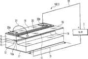
作为本发明的第五实施例,将相关于参考图8A的总体配置描述采用本发明第一至第四实施例所述的可调半导体激光器1之一的气体检测器。As a fifth embodiment of the present invention, a gas detector employing one of the
图8A是作为第五实施例的采用根据本发明的可调半导体激光器的气体检测器的一个示例的配置示意图。FIG. 8A is a schematic configuration diagram of an example of a gas detector employing a tunable semiconductor laser according to the present invention as a fifth embodiment.
如图8A所示,在用于进行气体检测的气体检测器30中,衬底33设置在构成半导体激光器模块31的圆柱外壳32内。As shown in FIG. 8A , in a gas detector 30 for gas detection, a substrate 33 is provided in a cylindrical case 32 constituting a
由珀耳帖(Peltier)装置形成的温度控制装置35安装到设置在衬底33上的基体34的表面上。A
此外,将本发明上述第一至第四实施例之一的可调半导体激光器1安装在设置于温度控制装置35上的安装基体36上。In addition, the
在此情况下,可调半导体激光器1布置为能够沿圆柱外壳32的中心轴辐射激光束到外部。In this case, the
在朝向检测目标辐射激光束以用于测量检测目标气体的浓度的情况下,通过将在下面详细描述的图8B所示的激光器驱动控制单元50的温度稳定PID电路55,可调半导体激光器1由珀耳帖装置形成的温度控制装置35进行温度控制,由此将激光束控制到与检测目标气体匹配的波长。In the case where a laser beam is irradiated toward the detection target for measuring the concentration of the detection target gas, the
在气体检测器30具有图8A所示配置的情况下,来自可调半导体激光器1的激光束辐射到两侧的检测目标气体和参考气体。In the case of the gas detector 30 having the configuration shown in FIG. 8A , the laser beam from the
用于将辐射到检测目标气体侧和参考气体侧的各激光束射线会聚成平行束的会聚透镜37和38设置为在安装基体36上在可调半导体激光器1的两侧沿透镜光轴定位。Converging
因此,从可调半导体激光器1到检测目标气体侧的激光束通过会聚透镜37和为保护半导体激光器模块31而设置的保护玻璃39输出到外部,然后辐射到检测空间。Therefore, the laser beam from the
从可调半导体激光器1到参考气体侧的激光束通过会聚透镜38形成为平行束,并穿过参考气体单元40被光检测器41检测。The laser beam from the
参考气体单元40是填充以用作参考气体的检测目标气体的单元,并使用如下。根据辐射到参考气体侧并穿过参考气体单元40被光检测器41检测的激光束的检测输出,通过使用将在下面描述的图8B所示的激光器驱动控制单元50的波长稳定控制电路54,将从可调半导体激光器1辐射的激光束的波长调节到检测目标气体的吸收线。The
光检测器41检测辐射到检测空间的激光束的反射和返回激光束,然后将接收到的激光束转换成电信号(电流),并将电信号(电流)提供到将在下面详细描述的图8C所示的气体检测单元60。The
如以下进一步描述的,气体检测单元60检测来自光检测器41转换的电信号的基谐波电平和倍谐波电平,用倍谐波电平除以基谐波电平,然后进行测量,从而根据除法得到的值检测检测目标气体存在与否、浓度等。As further described below, the
图8A至8C以及其相关描述已经省略了本发明第一至第四实施例之一的可调半导体激光器1的结构说明和描述,其中,如上所述,电极对17和18以及加热部分20(或者20A和20B)串联连接到单个外部电源2,由此驱动电流同步地从单个外部电源2提供到电极对17和18与加热部分20(或者20A和20B)。8A to 8C and their related descriptions have omitted the structural illustration and description of the
图8B是示出半导体激光器模块31和激光器驱动控制单元50的总体结构的图。FIG. 8B is a diagram showing the overall configuration of the
激光器驱动控制单元50配置为包括电流-电压转换器(converter)51、基谐波信号放大器52、信号微分检测器(signal differentiation detector)53、波长稳定控制电路54、温度稳定PID电路55和激光器驱动电路56。The laser
电流-电压转换器51将所接收的来自光检测器41的电信号转换成电压。基谐波信号放大器52放大由电流-电压转换器51转换的电压。信号微分检测器53进行由基谐波信号放大器52放大的电压波形的微分并产生从参考气体的吸收中心波长λ0偏移的偏移信号。The current-
波长稳定控制电路54将可调半导体激光器1的发射波长λ稳定到参考气体的吸收中心波长λ0。The wavelength
更特别地,波长稳定控制电路54将从信号微分检测器53接收到的偏移信号转换成可调半导体激光器1的温度,将结果输出到温度稳定PID电路55,并根据表示从其偏移的偏移信号将控制信号输出到参考气体单元40。More specifically, the wavelength
温度稳定PID电路55控制由珀耳帖装置构成的温度控制装置35。更特别地,根据来自波长稳定控制电路54的温度信号,温度稳定PID电路55提供PID控制,使得可调半导体激光器1被设置到引起在期望波长处振荡的温度,从而稳定地将可调半导体激光器1的温度保持在期望温度处。The temperature
相关于与中心电流值(偏置电流值)或者可调半导体激光器1的振荡波长对应于参考气体(待测气体)的吸收特性的吸收中心波长的电流值对应的中心,激光器驱动电路56施加具有预定振幅的调制信号b和调制频率到包括在半导体激光器模块31中的可调半导体激光器1。With respect to the center corresponding to the center current value (bias current value) or the current value corresponding to the absorption center wavelength of the oscillation wavelength of the
结果,其波长可根据与吸收中心波长相关的预定振幅和频率而改变的激光束从半导体激光器模块31输出。As a result, a laser beam whose wavelength can be changed according to a predetermined amplitude and frequency related to the absorption center wavelength is output from the
根据来自波长稳定控制电路54的温度信号,激光器驱动电路56控制中心电流值(偏置电流值)从而能够获得由半导体激光器模块31输出的激光束的上述波长特性。Based on the temperature signal from the wavelength
由此,在第五实施例的气体检测器中,使从可调半导体激光器1辐射的激光束穿过填充有与测量目标气体相同的气体的参考气体单元40,其中可调半导体激光器1的温度和施加到可调半导体激光器1的调制信号b的中心电流值(偏置电流值)被自动控制,使得激光束的中心波长与参考气体(测量目标气体)的吸收特性的吸收中心波长匹配。Thus, in the gas detector of the fifth embodiment, the laser beam irradiated from the
图8C是显示图8A所示的气体检测器和气体检测单元60的总体结构的图。FIG. 8C is a diagram showing the overall structure of the gas detector and the
参考图8C,从半导体激光器模块31输出的与吸收中心波长相关地波长调制激光束在穿过测量目标气体时相应于吸收特性被吸收;之后,光检测器41接收的激光束被转换成电(电流)信号c,并输入到气体检测单元60。Referring to FIG. 8C, the wavelength-modulated laser beam correlated with the absorption center wavelength output from the
为了便于描述,图8C单独示出半导体激光器模块31的光检测器41。For convenience of description, FIG. 8C shows the
已经参考图8B描述了激光器驱动控制单元50的详细构造及其操作。The detailed configuration of the laser
气体检测单元60包括电流-电压转换器61、基谐波信号检测器(fundamental harmonic signal detector)62、倍谐波信号检测器(doubleharmonic signal detector)63和驱动器64。The
电流-电压转换器61将输入电流的电(电流)信号c转换成电压的电信号c,并将已转换的信号传送到基谐波信号检测器62和倍谐波信号检测器63。The current-
基谐波信号检测器62取出基谐波信号d1,其是包含于输入电信号c中的调制频率的信号分量,并将取出的信号输送到驱动器64。The fundamental
倍谐波信号检测器63取出倍谐波信号d2,其是包含于输入电信号c中的调制频率的倍频的信号分量,并将取出的信号输送到驱动器64。The double
驱动器64计算倍谐波信号d2的振幅D2与基谐波信号d1的振幅D1之间的比率(D2/D1),并输出所计算的比率(D2/D1)作为与相应气体浓度对应的检测值D(=D2/D1)。The
如上所述,构造本发明的可调半导体激光器1,使电极对17和18以及加热部分20(或者20A和20B)串联连接到单个的外部电源2,由此将驱动电流从单个外部电源2同时提供到电极对17和18以及加热部分20(或者20A和20B)。As described above, the
因此,在采用本发明的可调半导体激光器1的TDLAS方案的气体检测器的情况下,可以增大折射率变化,从而利用单路电流控制波长在期望的可调波长范围内并控制激光器输出。Therefore, in the case of the gas detector adopting the TDLAS scheme of the
此外,在控制激光输出和波长的情况下,由于共用单个电源,因此只需要提供单个电源来完成操作。Furthermore, in the case of controlling the laser output and wavelength, only a single power supply needs to be supplied to complete the operation since a single power supply is shared.
因此,简化了本发明可调半导体激光器1的构造,使得可调半导体激光器1可以通过引入到便携式气体检测器30中而被使用,便携式气体检测器30中功耗低,且外壳中的部件安装空间、电源容量等被限制。Therefore, the structure of the
此外,当采用第一实施例的可调半导体激光器时,形成如下结构,其中有源区A(有源层12)不直接被加热部分20加热,由此可以增长器件自身的寿命。Furthermore, when the tunable semiconductor laser of the first embodiment is employed, a structure is formed in which the active region A (active layer 12) is not directly heated by the
在第三或第四实施例的各可调半导体激光器1C或1D中,衍射光栅14设置在抗反射膜21所夹区域中在一端或两端中的每一个。In each
然而,本发明不限于这样的结构,本发明的结构(其中电极对和加热部分串联连接到单个电源的结构)还可以在光波导中具有至少单个衍射光栅区域的可调半导体激光器中采用。However, the present invention is not limited to such a structure, and the structure of the present invention (a structure in which electrode pairs and a heating portion are connected in series to a single power source) can also be employed in a tunable semiconductor laser having at least a single diffraction grating region in an optical waveguide.
更特别地,本发明的可调半导体激光器1的结构可以如此,优选地,加热部分20(或者20A和20B)设置在没有模式调变(mode hopping)的区域中,电极对17和18以及加热部分20(20A、20B)串联连接到单个外部电源。More particularly, the structure of the
虽然已经在上面描述了本发明的优选实施例,但本发明不受优选实施例的描述和附图的限制。Although the preferred embodiments of the present invention have been described above, the present invention is not limited by the description and drawings of the preferred embodiments.
当然,本领域技术人员根据优选实施例可完成的其他实施例、示例、操作技术全部包括在本发明的范围内。Of course, other embodiments, examples, and operation techniques that can be accomplished by those skilled in the art according to the preferred embodiment are all within the scope of the present invention.
Claims (28)
Applications Claiming Priority (2)
| Application Number | Priority Date | Filing Date | Title |
|---|---|---|---|
| JP2005077373AJP4231854B2 (en) | 2005-03-17 | 2005-03-17 | Semiconductor laser element and gas detector |
| JP077373/2005 | 2005-03-17 |
Publications (2)
| Publication Number | Publication Date |
|---|---|
| CN1957508A CN1957508A (en) | 2007-05-02 |
| CN100481659Ctrue CN100481659C (en) | 2009-04-22 |
Family
ID=36991771
Family Applications (1)
| Application Number | Title | Priority Date | Filing Date |
|---|---|---|---|
| CNB2006800002566AExpired - Fee RelatedCN100481659C (en) | 2005-03-17 | 2006-03-17 | Tunable semiconductor laser, method of manufacturing the same, and gas detector using the same |
Country Status (6)
| Country | Link |
|---|---|
| US (1) | US7620078B2 (en) |
| EP (1) | EP1737089B1 (en) |
| JP (1) | JP4231854B2 (en) |
| KR (1) | KR100799782B1 (en) |
| CN (1) | CN100481659C (en) |
| WO (1) | WO2006098427A1 (en) |
Cited By (1)
| Publication number | Priority date | Publication date | Assignee | Title |
|---|---|---|---|---|
| CN105765799A (en)* | 2013-11-30 | 2016-07-13 | 统雷量子电子有限公司 | Tunable semiconductor radiation source |
Families Citing this family (35)
| Publication number | Priority date | Publication date | Assignee | Title |
|---|---|---|---|---|
| JP4231854B2 (en)* | 2005-03-17 | 2009-03-04 | アンリツ株式会社 | Semiconductor laser element and gas detector |
| US20100168405A1 (en) | 2006-08-11 | 2010-07-01 | Toyo Boseki Kabushiki Kaisha | Activator including biosurfactant as active ingredient, mannosyl erythritol lipid, and production method thereof |
| JP4850757B2 (en) | 2007-03-08 | 2012-01-11 | 日本電信電話株式会社 | Wavelength tunable semiconductor laser device, control device and control method thereof |
| DE102007039219B4 (en)* | 2007-08-20 | 2010-04-22 | Fraunhofer-Gesellschaft zur Förderung der angewandten Forschung e.V. | Spectrally tunable laser module |
| KR100959170B1 (en)* | 2008-02-26 | 2010-05-24 | 한국광기술원 | Fabrication method of self-oscillating multi-region DVF laser diode with integrated metal thin film heater |
| US8149890B2 (en)* | 2008-12-04 | 2012-04-03 | Electronics And Telecommunications Research Institute | Multiple distributed feedback laser devices |
| US7864824B2 (en) | 2008-12-04 | 2011-01-04 | Electronics And Telecommunications Research Institute | Multiple distributed feedback laser devices |
| EP3739635B1 (en)* | 2010-06-30 | 2022-03-09 | Alcatel Lucent | A device comprising an active component and associated electrodes and a method of manufacturing such device |
| JP5919682B2 (en)* | 2011-08-26 | 2016-05-18 | 富士通株式会社 | Semiconductor laser device |
| DE102012202893B3 (en)* | 2012-02-27 | 2013-01-17 | Siemens Aktiengesellschaft | Method for measuring concentration of gas component in measuring gas for visual gas analysis, involves triggering and producing current signals and burst-current signals such that signals are modified with directly generated current signals |
| JP6155770B2 (en)* | 2013-03-29 | 2017-07-05 | 富士通株式会社 | Optical element and optical module |
| USD734187S1 (en)* | 2013-06-24 | 2015-07-14 | New Cosmos Electric Co., Ltd. | Gas detector |
| JP6277660B2 (en)* | 2013-10-16 | 2018-02-14 | 住友電気工業株式会社 | Full duplex optical transceiver |
| US9537287B2 (en) | 2014-10-08 | 2017-01-03 | Futurewei Technologies, Inc. | Thermal compensation for burst-mode laser wavelength drift |
| US9246307B1 (en)* | 2014-10-08 | 2016-01-26 | Futurewei Technologies, Inc. | Thermal compensation for burst-mode laser wavelength drift |
| US20180083421A1 (en) | 2015-03-06 | 2018-03-22 | Apple Inc. | Independent control of emission wavelength and output power of a semiconductor laser |
| US11437779B2 (en)* | 2015-04-30 | 2022-09-06 | Apple Inc. | Vernier effect DBR lasers incorporating integrated tuning elements |
| DE102015119226A1 (en)* | 2015-11-09 | 2017-05-11 | Osram Opto Semiconductors Gmbh | Semiconductor laser diode |
| KR102729488B1 (en)* | 2016-11-08 | 2024-11-12 | 삼성전자주식회사 | Spectrometer, apparatus and method for measuring bio-information |
| CN107093839B (en)* | 2017-06-14 | 2024-04-09 | 西安炬光科技股份有限公司 | Semiconductor laser wavelength stabilizing system and implementation method |
| EP3688849A1 (en) | 2017-09-28 | 2020-08-05 | Apple Inc. | Laser architectures using quantum well intermixing techniques |
| US11552454B1 (en)* | 2017-09-28 | 2023-01-10 | Apple Inc. | Integrated laser source |
| CN108336634A (en)* | 2018-04-17 | 2018-07-27 | 大连藏龙光电子科技有限公司 | Tunable Laser Transmitter Heat Sink for Next Generation PON Technology |
| US11171464B1 (en) | 2018-12-14 | 2021-11-09 | Apple Inc. | Laser integration techniques |
| CN111089850B (en)* | 2020-02-17 | 2021-09-28 | 北京航空航天大学 | Multi-component concentration estimation method based on single-component absorption spectrum |
| KR102426648B1 (en)* | 2020-10-20 | 2022-07-29 | 한국과학기술연구원 | Integrated photoacoustic gas sensor and method for manufacturing the same |
| CN112713504A (en)* | 2021-01-11 | 2021-04-27 | 宁波元芯光电子科技有限公司 | Thermally tuned DFB laser |
| US12204155B2 (en) | 2021-09-24 | 2025-01-21 | Apple Inc. | Chip-to-chip optical coupling for photonic integrated circuits |
| CN113625381B (en)* | 2021-10-08 | 2022-01-04 | 中国工程物理研究院流体物理研究所 | Adjustable surface type body Bragg grating and spectral imager |
| CN114199809B (en)* | 2021-11-23 | 2024-02-09 | 南京大学 | Monolithic integrated infrared laser gas detection device |
| WO2023248412A1 (en)* | 2022-06-23 | 2023-12-28 | 日本電信電話株式会社 | Wavelength-variable laser, wavelength-variable laser module, and method for producing layered structure of wavelength-variable laser |
| US12426139B1 (en) | 2022-06-27 | 2025-09-23 | Apple Inc. | Feedback control of a diode element |
| US12159516B1 (en)* | 2023-09-05 | 2024-12-03 | Bank Of America Corporation | Detecting a hardware failure using optical absorption spectroscopy |
| CN117578172B (en)* | 2024-01-17 | 2024-05-17 | 山东中芯光电科技有限公司 | Wavelength expansion method and system based on DBR laser |
| CN118336512B (en)* | 2024-06-12 | 2024-09-03 | 天津市极光创新智能科技有限公司 | TDLAS middle infrared laser control system and method |
Citations (3)
| Publication number | Priority date | Publication date | Assignee | Title |
|---|---|---|---|---|
| CN1396685A (en)* | 2001-07-05 | 2003-02-12 | 朗迅科技公司 | Adjustable wavelength laser |
| CN1424794A (en)* | 2003-01-03 | 2003-06-18 | 复旦大学 | Semiconductor laser with continuously adjustable wavelength and preparation thereof |
| JP2003318483A (en)* | 2002-02-19 | 2003-11-07 | Mitsubishi Electric Corp | Tunable semiconductor laser |
Family Cites Families (12)
| Publication number | Priority date | Publication date | Assignee | Title |
|---|---|---|---|---|
| JPH03196587A (en)* | 1989-12-25 | 1991-08-28 | Mitsubishi Electric Corp | Electrode split type semiconductor laser |
| JP3152424B2 (en) | 1990-07-13 | 2001-04-03 | 株式会社日立製作所 | Tunable semiconductor laser |
| JP2804838B2 (en)* | 1990-10-11 | 1998-09-30 | 国際電信電話株式会社 | Tunable semiconductor laser |
| JP2536390B2 (en) | 1993-04-21 | 1996-09-18 | 日本電気株式会社 | Semiconductor laser and manufacturing method thereof |
| JP2713256B2 (en) | 1995-07-21 | 1998-02-16 | 日本電気株式会社 | Tunable semiconductor laser used for optical communication etc. |
| JP3990745B2 (en) | 1995-09-06 | 2007-10-17 | アンリツ株式会社 | Semiconductor optical module |
| JP2001142037A (en)* | 1999-11-17 | 2001-05-25 | Oki Electric Ind Co Ltd | Method of manufacturing field effect optical modulator and semiconductor optical element |
| AU2002245062A1 (en)* | 2000-10-30 | 2002-07-30 | Santur Corporation | Laser thermal tuning |
| JP3773880B2 (en) | 2002-06-27 | 2006-05-10 | アンリツ株式会社 | Distributed feedback semiconductor laser |
| US20040190580A1 (en)* | 2003-03-04 | 2004-09-30 | Bardia Pezeshki | High-yield high-precision distributed feedback laser based on an array |
| JP2005106521A (en) | 2003-09-29 | 2005-04-21 | Anritsu Corp | Semiconductor laser unit and gas concentration measuring device |
| JP4231854B2 (en)* | 2005-03-17 | 2009-03-04 | アンリツ株式会社 | Semiconductor laser element and gas detector |
- 2005
- 2005-03-17JPJP2005077373Apatent/JP4231854B2/ennot_activeExpired - Fee Related
- 2006
- 2006-03-17CNCNB2006800002566Apatent/CN100481659C/ennot_activeExpired - Fee Related
- 2006-03-17WOPCT/JP2006/305360patent/WO2006098427A1/enactiveApplication Filing
- 2006-03-17KRKR1020067024014Apatent/KR100799782B1/ennot_activeExpired - Fee Related
- 2006-03-17EPEP06729350Apatent/EP1737089B1/ennot_activeExpired - Fee Related
- 2006-03-17USUS11/578,637patent/US7620078B2/ennot_activeExpired - Fee Related
Patent Citations (3)
| Publication number | Priority date | Publication date | Assignee | Title |
|---|---|---|---|---|
| CN1396685A (en)* | 2001-07-05 | 2003-02-12 | 朗迅科技公司 | Adjustable wavelength laser |
| JP2003318483A (en)* | 2002-02-19 | 2003-11-07 | Mitsubishi Electric Corp | Tunable semiconductor laser |
| CN1424794A (en)* | 2003-01-03 | 2003-06-18 | 复旦大学 | Semiconductor laser with continuously adjustable wavelength and preparation thereof |
Cited By (2)
| Publication number | Priority date | Publication date | Assignee | Title |
|---|---|---|---|---|
| CN105765799A (en)* | 2013-11-30 | 2016-07-13 | 统雷量子电子有限公司 | Tunable semiconductor radiation source |
| CN105765799B (en)* | 2013-11-30 | 2020-06-23 | 统雷量子电子有限公司 | Tunable semiconductor radiation source |
Also Published As
| Publication number | Publication date |
|---|---|
| EP1737089B1 (en) | 2011-12-21 |
| EP1737089A1 (en) | 2006-12-27 |
| US7620078B2 (en) | 2009-11-17 |
| KR100799782B1 (en) | 2008-01-31 |
| CN1957508A (en) | 2007-05-02 |
| JP4231854B2 (en) | 2009-03-04 |
| WO2006098427A1 (en) | 2006-09-21 |
| US20090086206A1 (en) | 2009-04-02 |
| JP2006261424A (en) | 2006-09-28 |
| KR20070015201A (en) | 2007-02-01 |
| EP1737089A4 (en) | 2011-02-02 |
Similar Documents
| Publication | Publication Date | Title |
|---|---|---|
| CN100481659C (en) | Tunable semiconductor laser, method of manufacturing the same, and gas detector using the same | |
| US8563991B2 (en) | Optical semiconductor device, laser chip and laser module | |
| US9935426B2 (en) | Optical semiconductor device | |
| US8279907B2 (en) | Semiconductor laser device and method for controlling semiconductor laser | |
| JP2019087572A (en) | Wavelength variable light source and optical semiconductor device | |
| US9025628B2 (en) | Semiconductor laser | |
| US8194710B2 (en) | Semiconductor laser with heater | |
| US11050218B2 (en) | Method to tune emission wavelength of laser apparatus | |
| JP6308089B2 (en) | Control method of optical semiconductor device | |
| US7656927B2 (en) | Optical semiconductor element and optical semiconductor device | |
| US20190052054A1 (en) | Laser arrangement, method for controlling laser and measuring method | |
| JP2009081321A (en) | Wavelength stabilized laser apparatus, method for the same, and raman amplifier equipped with wavelength stabilized laser apparatus | |
| JP2015088675A (en) | Method for controlling wavelength variable laser | |
| JP6382506B2 (en) | Control method of wavelength tunable laser | |
| JP5303580B2 (en) | Optical semiconductor device, laser chip and laser module | |
| JP2024114192A (en) | Tunable laser device and wavelength control method for tunable laser device |
Legal Events
| Date | Code | Title | Description |
|---|---|---|---|
| C06 | Publication | ||
| PB01 | Publication | ||
| C10 | Entry into substantive examination | ||
| SE01 | Entry into force of request for substantive examination | ||
| C14 | Grant of patent or utility model | ||
| GR01 | Patent grant | ||
| CF01 | Termination of patent right due to non-payment of annual fee | ||
| CF01 | Termination of patent right due to non-payment of annual fee | Granted publication date:20090422 Termination date:20160317 |