CN100477217C - Plasma damage protection circuit - Google Patents
Plasma damage protection circuitDownload PDFInfo
- Publication number
- CN100477217C CN100477217CCNB2005100761658ACN200510076165ACN100477217CCN 100477217 CCN100477217 CCN 100477217CCN B2005100761658 ACNB2005100761658 ACN B2005100761658ACN 200510076165 ACN200510076165 ACN 200510076165ACN 100477217 CCN100477217 CCN 100477217C
- Authority
- CN
- China
- Prior art keywords
- word line
- semiconductor substrate
- assembly
- transistor
- electric charge
- Prior art date
- Legal status (The legal status is an assumption and is not a legal conclusion. Google has not performed a legal analysis and makes no representation as to the accuracy of the status listed.)
- Expired - Fee Related
Links
- 239000004065semiconductorSubstances0.000claimsabstractdescription81
- 239000000758substrateSubstances0.000claimsabstractdescription77
- 238000000034methodMethods0.000claimsabstractdescription20
- 230000015654memoryEffects0.000claimsdescription45
- 238000004519manufacturing processMethods0.000claimsdescription22
- 230000000694effectsEffects0.000claimsdescription4
- 230000002265preventionEffects0.000abstract1
- 238000010586diagramMethods0.000description9
- 238000013461designMethods0.000description3
- 238000002347injectionMethods0.000description3
- 239000007924injectionSubstances0.000description3
- 239000003989dielectric materialSubstances0.000description2
- 239000002184metalSubstances0.000description2
- 238000012986modificationMethods0.000description2
- 230000004048modificationEffects0.000description2
- 238000012545processingMethods0.000description2
- 230000008021depositionEffects0.000description1
- 238000005530etchingMethods0.000description1
- 239000000463materialSubstances0.000description1
- 229920002120photoresistant polymerPolymers0.000description1
- 230000001012protectorEffects0.000description1
- 230000005612types of electricityEffects0.000description1
Images


Classifications
- G—PHYSICS
- G11—INFORMATION STORAGE
- G11C—STATIC STORES
- G11C8/00—Arrangements for selecting an address in a digital store
- G11C8/08—Word line control circuits, e.g. drivers, boosters, pull-up circuits, pull-down circuits, precharging circuits, for word lines
Landscapes
- Engineering & Computer Science (AREA)
- Microelectronics & Electronic Packaging (AREA)
- Semiconductor Memories (AREA)
Abstract
Description
Translated fromChinese技术领域technical field
本发明是有关于一种集成电路组件,且特别是有关于一种避免集成电路在制造过程中遭受等离子体损害的组件。The present invention relates to an integrated circuit assembly, and more particularly to an assembly for protecting integrated circuits from plasma damage during the manufacturing process.
背景技术Background technique
保护集成电路免于遭受等离子体损害为许多从事保护组件门电路设计者所热衷的课题。集成电路的制造过程通常包括等离子体处理工艺。例如金属蚀刻的后端(backend)处理、光阻材料后端剥除(stripping)以及介电质沉积等都会使用等离子体在欲处理的结构表面感应电荷。由等离子体感应产生的电荷会破坏组件本身与工作效益有关的基本结构。例如使用于闪存的通道介电质以与门极介电质就会遭受等离子体感应电荷的破坏。另外,使用于N位存储器SONOS(可捕捉电荷捕捉结构不同位置电荷的电荷捕捉存储单元)以及PHINES的电荷存储结构特别容易遭受等离子体感应工艺的破坏。Protecting integrated circuits from plasma damage is a hot topic for many designers engaged in protecting component gates. The fabrication process of integrated circuits often includes plasma processing processes. For example, backend processing of metal etching, stripping of photoresist material, and dielectric deposition etc. all use plasma to induce charge on the surface of the structure to be processed. The charge induced by the plasma destroys the basic structure of the component itself related to the working efficiency. For example, channel dielectrics and gate dielectrics used in flash memory are damaged by plasma-induced charges. In addition, the charge storage structures used in N-bit memories SONOS (charge trapping memory cells capable of trapping charges at different positions of the charge trapping structure) and PHINES are particularly susceptible to damage by plasma-induced processes.
等离子体感应电荷可以是正电荷或者是负电荷,而等离子体感应电荷的类型不同所造成的集成电路破坏程度也不同。Plasma-induced charges can be positive or negative, and different types of plasma-induced charges cause different degrees of damage to integrated circuits.
如图1所示,在公知的半导体存储器集成电路中,每一个字线(Word Line)驱动器101包括各自的保护电路,例如是CMOS晶体管对102。字线驱动器101在存储器操作过程中提供字线106不同的操作电压。CMOS晶体管对102包括PMOS 103及NMOS 105,可将等离子体感应电荷传导至半导体衬底。正电荷通过PMOS 103来传导,而负电荷则通过NMOS 105传导。字线驱动器的每一条字线具有保护电路,例如是CMOS晶体管对。然而,这种设计方式将占用大量芯片体积并降低电路密度。因此,这种等离子体保护电路设计将有碍于集成电路尺寸持续小型化的趋势。As shown in FIG. 1 , in a known semiconductor memory integrated circuit, each word line (Word Line)
发明内容Contents of the invention
有鉴于此,本发明的目的就是在提供一种等离子体损害保护电路,用以保护集成电路避免于制造过程中遭受等离子体损害。In view of this, the object of the present invention is to provide a plasma damage protection circuit for protecting integrated circuits from plasma damage during the manufacturing process.
根据本发明的目的,提出一种集成电路,包括半导体衬底、存储器阵列、多条字线以及多个字线驱动器。存储器阵列连接于半导体衬底。各字线连接于存储器阵列。各字线驱动器包括一组件,且在存储器操作中该组件耦接一电压到这些字线驱动器的至少一字线。其中当制造中电荷产生于字线时,该组件连接至半导体衬底,且电荷由字线通过组件传导至半导体衬底。According to the purpose of the present invention, an integrated circuit is provided, including a semiconductor substrate, a memory array, a plurality of word lines and a plurality of word line drivers. The memory array is connected to the semiconductor substrate. Each word line is connected to the memory array. Each wordline driver includes a component that couples a voltage to at least one wordline of the wordline drivers during memory operation. Wherein when charge is generated in the word line during manufacture, the component is connected to the semiconductor substrate, and the charge is conducted from the word line to the semiconductor substrate through the component.
根据本发明的目的,提出一种集成电路,包括半导体衬底、存储器阵列、多条字线、多个字线驱动器以及一组件。存储器阵列连接半导体衬底。各字线连接存储器阵列。多个字线驱动器连接这些字线。该组件则连接字线驱动器。其中当制造中电荷产生于字线时,电荷由这些字线通过至少该组件传导至半导体衬底。According to the purpose of the present invention, an integrated circuit is provided, including a semiconductor substrate, a memory array, a plurality of word lines, a plurality of word line drivers and a component. The memory array is connected to the semiconductor substrate. Each word line is connected to the memory array. A plurality of wordline drivers connect the wordlines. The component is connected to the word line driver. Wherein when charges are generated in the word lines during manufacture, the charges are conducted from the word lines to the semiconductor substrate through at least the component.
根据本发明的目的,提出一种集成电路,包括半导体衬底、存储器阵列、多条字线、多个字线驱动器以及一组件。存储器阵列连接半导体衬底。各字线连接存储器阵列。各字线驱动器包括一字线驱动器组件,于存储器操作中字线驱动器组件耦接一电压到至少这些字线驱动器的一字线,且字线驱动器组件连接半导体衬底以及其中至少一字线。组件则连接这些字线驱动器。其中当制造中电荷产生于字线时,电荷由字线通过至少该组件及字线驱动器组件其中的一传导至半导体衬底。According to the purpose of the present invention, an integrated circuit is provided, including a semiconductor substrate, a memory array, a plurality of word lines, a plurality of word line drivers and a component. The memory array is connected to the semiconductor substrate. Each word line is connected to the memory array. Each word line driver includes a word line driver unit. The word line driver unit couples a voltage to at least one word line of the word line drivers during memory operation, and the word line driver unit is connected to the semiconductor substrate and at least one word line therein. Components are connected to these word line drivers. Wherein when charge is generated in the word line during manufacture, the charge is conducted from the word line to the semiconductor substrate through at least one of the component and the word line driver component.
根据本发明的目的,提出一种制造集成电路组件的方法,包括提供一半导体衬底;形成一存储器阵列,以连接半导体衬底;形成多条字线,以连接存储器阵列;形成多个字线驱动器,以连接这些字线,其中各字线驱动器包括一组件,且于存储器操作中该组件耦接一电压到这些字线驱动器的至少一字线;以及当制造中电荷产生于字线时,将电荷由这些字线通过该组件传导至半导体衬底。According to the purpose of the present invention, a method for manufacturing integrated circuit components is proposed, including providing a semiconductor substrate; forming a memory array to connect the semiconductor substrate; forming a plurality of word lines to connect the memory array; forming a plurality of word lines drivers to connect the word lines, wherein each word line driver includes a component, and the component couples a voltage to at least one word line of the word line drivers during memory operation; and when charge is generated on the word line during manufacture, Charge is conducted from the word lines through the assembly to the semiconductor substrate.
根据本发明的目的,提出一种制造集成电路组件的方法,包括提供一半导体衬底;形成一存储器阵列,以连接半导体衬底;形成多条字线,以连接存储器阵列;形成多个字线驱动器,以连接这些字线;形成一组件,以连接这些字线驱动器;以及当制造中电荷产生于这些字线时,将电荷由这些字线通过至少该组件传导至半导体衬底。According to the purpose of the present invention, a method for manufacturing integrated circuit components is proposed, including providing a semiconductor substrate; forming a memory array to connect the semiconductor substrate; forming a plurality of word lines to connect the memory array; forming a plurality of word lines a driver for connecting the word lines; forming a component for connecting the word line drivers; and conducting charge from the word lines to the semiconductor substrate through at least the component when charges are generated in the word lines during manufacture.
根据本发明的目的,提出一种制造集成电路组件的方法,包括提供一半导体衬底;形成一存储器阵列,以连接半导体衬底;形成多条字线,以连接存储器阵列;形成多个字线驱动器,以连接这些字线,各字线驱动器包括一字线驱动器组件。其中于存储器操作中字线驱动器组件耦接一电压到这些字线驱动器的至少一字线;形成一组件,以连接这些字线驱动器;当制造中电荷产生于这些字线时,将电荷由这些字线通过至少字线驱动器组件传导至半导体衬底;以及当制造中电荷产生于这些字线时,将电荷由这些字线驱动器的各字线通过至少该组件传导至半导体衬底。According to the purpose of the present invention, a method for manufacturing integrated circuit components is proposed, including providing a semiconductor substrate; forming a memory array to connect the semiconductor substrate; forming a plurality of word lines to connect the memory array; forming a plurality of word lines drivers to connect the word lines, and each word line driver includes a word line driver component. wherein the word line driver assembly couples a voltage to at least one word line of the word line drivers during memory operation; forms an assembly to connect the word line drivers; and transfers the charge from the word lines when charges are generated in the word lines during manufacture conducting lines to the semiconductor substrate through at least the wordline driver assembly; and conducting charge from each of the wordlines of the wordline drivers to the semiconductor substrate through at least the assembly when charge is generated in the wordlines during manufacture.
某些实例中每个字线驱动器包括连接半导体衬底及字线的一组件,例如是一晶体管。通过此晶体管电荷可由字线传导至半导体衬底。通过使用字线驱动器的一晶体管,可有效节省集成电路的使用空间。例如在正常的存储器操作中,晶体管将一供电电压耦接至字线。晶体管具有某一种电荷类型,且传导同一类型的电荷。例如产生于字线的空穴由字线通过字线驱动器中至少一P型晶体管传导至半导体衬底。而产生于字线的电子由字线通过字线驱动器中至少一N型晶体管传导至半导体衬底。其中一实例中晶体管形成于连接半导体衬底的一半导体阱中,且晶体管的电流负载端,例如是源极或漏极,则连接至字线。In some embodiments, each wordline driver includes a component, such as a transistor, connecting the semiconductor substrate and the wordline. Through this transistor charge can be conducted from the word line to the semiconductor substrate. By using a transistor of the word line driver, the use space of the integrated circuit can be effectively saved. For example, during normal memory operation, the transistor couples a supply voltage to the word line. Transistors have a certain type of charge and conduct the same type of charge. For example, holes generated in the word line are conducted from the word line to the semiconductor substrate through at least one P-type transistor in the word line driver. The electrons generated in the word line are conducted from the word line to the semiconductor substrate through at least one N-type transistor in the word line driver. In one example, the transistor is formed in a semiconductor well connected to the semiconductor substrate, and the current carrying terminal of the transistor, such as the source or the drain, is connected to the word line.
某些实例中,电荷通过两个字线驱动器以及连接字线驱动器的一组件传导。某一实例中,同一类型的电通过字线驱动器以及连接字线驱动器的组件来传导。通过提供由字线至半导体衬底的不同传导电荷路径,本发明可对集成电路提供更多的保护,且使用到较少的集成电路空间。在另一实例中,某一类型电荷通过该组件传导,而另一类型电荷则通过字线驱动器传导,进而缩小集成电路的使用空间。例如,产生于字线的电子通过至少该组件传导至半导体衬底,而产生于字线的空穴则通过至少字线驱动器传导至半导体衬底。在另一实例中,产生于字线的空穴通过至少该组件传导至半导体衬底,而产生于字线的电子则通过至少字线驱动器传导至半导体衬底。In some examples, charge is conducted through two wordline drivers and a component connecting the wordline drivers. In one example, the same type of electricity is conducted through the wordline driver and components connected to the wordline driver. By providing a different conduction charge path from the word line to the semiconductor substrate, the present invention can provide more protection to the integrated circuit and use less integrated circuit space. In another example, a certain type of charge is conducted through the device, while another type of charge is conducted through the word line driver, thereby reducing the footprint of the integrated circuit. For example, electrons generated in the word line are conducted to the semiconductor substrate through at least the component, and holes generated in the word line are conducted to the semiconductor substrate through at least the word line driver. In another example, holes generated in the word line are conducted to the semiconductor substrate through at least the device, and electrons generated in the word line are conducted to the semiconductor substrate through at least the word line driver.
为让本发明的上述目的、特征、和优点能更明显易懂,下文特举一较佳实施例,并配合附图,详细说明如下:In order to make the above-mentioned purposes, features, and advantages of the present invention more comprehensible, a preferred embodiment is specifically cited below, together with the accompanying drawings, and the details are as follows:
附图说明Description of drawings
图1表示公知的半导体存储器集成电路图。FIG. 1 shows a diagram of a known semiconductor memory integrated circuit.
图2表示依照本发明一较佳实施例具有字线的一种电路图。Figure 2 shows a circuit diagram with word lines in accordance with a preferred embodiment of the present invention.
图3表示图2部份线路剖面图。Fig. 3 shows a sectional view of part of the circuit in Fig. 2 .
图4表示依照本发明一较佳实施例包括分别连接于不同字线的两个字线驱动器线路图。FIG. 4 shows a circuit diagram including two word line drivers respectively connected to different word lines according to a preferred embodiment of the present invention.
图5表示图4部份线路剖面图。Fig. 5 shows a sectional view of part of the circuit in Fig. 4 .
图6表示依照本发明较佳实施例连接不同字线的两个字字线驱动器线路图。FIG. 6 shows a circuit diagram of two word line drivers connected to different word lines according to a preferred embodiment of the present invention.
图7表示具有保护多个字线驱动器及字线的保护装置的集成电路部份线路平面图。FIG. 7 shows a partial circuit plan view of an integrated circuit with a protection device for protecting a plurality of word line drivers and word lines.
图8表示依照本发明较佳实施例集成电路的简化方块图。Figure 8 shows a simplified block diagram of an integrated circuit in accordance with a preferred embodiment of the present invention.
主要组件符号说明Explanation of main component symbols
101、201、401、402:字线驱动器101, 201, 401, 402: word line drivers
601、602、701、702:字线驱动器601, 602, 701, 702: word line drivers
102:CMOS晶体管对102: CMOS transistor pair
103:PMOS103: PMOS
105:NMOS105: NMOS
106、208、209、709、710、802:字线106, 208, 209, 709, 710, 802: word line
205、215、223、231:源极/漏极的一端205, 215, 223, 231: one end of source/drain
207、217、225、233:源极/漏极的另一端207, 217, 225, 233: the other end of the source/drain
211:P阱211: P well
213:N阱213: N well
220、240:NMOS晶体管220, 240: NMOS transistors
221:导线221: wire
230:PMOS晶体管230: PMOS transistor
235:结点235: node
250:接地参考点250: Ground reference point
261:电压NDIS261: Voltage NDIS
262:电压WLDRVSS262: Voltage WLDRVSS
263:电压AVX263: Voltage AVX
264:电压GWL264: Voltage GWL
265:电压PP265: Voltage PP
266:电压NP266: Voltage NP
105A及105B:保护用NMOS晶体管105A and 105B: NMOS transistors for protection
210:保护用PMOS晶体管210: PMOS transistor for protection
705:导线705: Wire
711:深度掺杂区711: Deeply doped region
720、730:半导体阱720, 730: semiconductor well
740:等离子体保护装置740: Plasma Protector
800:电荷捕捉元阵列800: Array of Charge Trapping Elements
801:行译码器/字线驱动器801: Row Decoder/Word Line Driver
803:列译码器803: column decoder
804:位线804: bit line
805:总线805: bus
806:检测放大器/数据输入结构806: Sense Amplifier/Data Input Structure
807:数据总线807: Data bus
808:偏压设置供电电压808: Bias setting supply voltage
809:偏压设置状态机构809: Bias Setting State Mechanism
810:等离子体损害保护装置810: Plasma Damage Protection
811:数据输入线811: Data input line
812:数据输出线812: data output line
850:集成电路850: integrated circuit
具体实施方式Detailed ways
接下来就以实施例来对本发明进行详细说明。值得注意的是,所参考的附图以简化的形式呈现而非实际的尺寸。Next, the present invention will be described in detail with examples. It is worth noting that the drawings referred to are presented in simplified form and not to actual dimensions.
虽然接下来参考实施例来公开本发明,然而当知所描述的实施例仅是用以举例说明的目的,不应用以限制本发明。而接下来以实施例来叙述的详细说明内容可包括任何的更动与修改以及等效的实施例,此皆落入本发明所定义的权利要求范围及精神中。Although the present invention is disclosed below with reference to the embodiments, it should be understood that the described embodiments are only for the purpose of illustration and should not be used to limit the present invention. The detailed description described in the following embodiments may include any changes, modifications and equivalent embodiments, which all fall within the scope and spirit of the claims defined by the present invention.
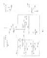
请参照图2,其表示依照本发明一较佳实施例具有字线的一种电路图。字线驱动器201包括两个NMOS晶体管220及240以及一个PMOS晶体管230。NMOS晶体管220中源极/漏极的一端205连接接地参考点250,以作为存储器操作中电压提供的参考点。NMOS晶体管220中源极/漏极的另一端207则连接至字线209。Please refer to FIG. 2, which shows a circuit diagram with word lines according to a preferred embodiment of the present invention. The
NMOS晶体管220的栅极连接至电压NDIS 261,用以于操作过程中导通或关断NMOS晶体管220。NMOS晶体管220的P阱211于操作过程中连接至电压WLDRVSS 262。NMOS晶体管220的N阱213则连接至电压AVX 263,以避免在操作过程中产生PN结(junction)效应。The gate of the
PMOS晶体管230中源极/漏极的一端215连接字线209。PMOS晶体管230中源极/漏极的另一端217连接电压GWL 264以进行例如是编程、删除及读取的存储器操作。PMOS晶体管230的N阱通过导线221连接至NMOS晶体管240的N阱。PMOS晶体管230的栅极则连接电压PP 265以于存储器操作中导通/关断PMOS晶体管230。One
NMOS晶体管240中源极及漏极的一端223连接PMOS晶体管230中源极/漏极的一端217。NMOS晶体管240中源极/漏极的另一端225连接字线209。如上所述,NMOS晶体管240的N阱通过导线221连接PMOS晶体管230的N阱。NMOS晶体管240的P阱于存储器操作中耦接电压WLDRVSS 262。NMOS晶体管240的栅极连接电压NP 266,以于存储器操作过程中导通/关断NMOS晶体管240。One
PMOS晶体管103连接每一个字线驱动器,并将等离子体感应电荷传导至半导体衬底。The
在制造过程中,电压PP 265、NDIS 261以及NP 266为浮接,因此NMOS晶体管220及240以及PMOS晶体管230的栅极为浮接。在制造工艺中,等离子体感应电荷由字线传导至半导体衬底。负电荷由字线209通过NMOS晶体管220传导至半导体衬底。因为在存储器操作中负电荷通过作为字线驱动电路201部份电路的NMOS晶体管220而不是通过用以保护字线驱动器受等离子体损害的额外NMOS晶体管105,于是可以节省大量的集成电路使用空间。正电荷由字线209通过PMOS晶体管103传导至半导体衬底。半导体衬底为整个集成电路的接地参考点250。因此,本发明可避免具有字线驱动电路的集成电路遭受具有正负两种极性的等离子体电荷破坏。During the manufacturing process,
当进行例如是读取、删除以及编程的存储器操作时,字线驱动器具有下列的电压特性。The word line driver has the following voltage characteristics when performing memory operations such as reading, erasing, and programming.
在删除模式中,由于NMOS晶体管220的栅极偏压NDIS=-4V,因此NMOS晶体管220不导通。In the erase mode, since the gate bias voltage of the
请参照图3,其表示图2部份线路剖面图。NMOS晶体管220中源极/漏极的一端205连接接地参考点250,作为存储器操作过程的供电电压参作点。NMOS晶体管220中源极/漏极的另一端207连接字线209。NMOS晶体管220形成于P阱211中。P阱211又形成于N阱213中,而N阱213则形成于作为接地点250的P型衬底。在制造过程中,等离子体感应负电荷由字线209通过NMOS晶体管220传导至作为接地点250的半导体衬底。在字线209上的等离子体感应负电荷造成字线209的电压低于P阱211的电压。而P阱211的电压相对于端点205为负值。因此,N+源极/漏极端205及207与P阱211通过少量的载流子注入传导电流,犹如一个工作于有源模式的双极结型晶体管(bipolar junction transistor)。Please refer to FIG. 3 , which shows a sectional view of part of the circuit in FIG. 2 . One
请参照图4,其表示依照本发明一较佳实施例包括分别连接于不同字线的两个字线驱动器线路图。字线驱动器401及402的线路与图2的字线驱动器201的线路相似。然而,在图4中,字线209及208分别连接于等离子体保护NMOS晶体管105A及105B。在制造过程中,等离子体感应负电荷由字线209通过NMOS晶体管105A传导至作为接地点250的半导体衬底。Please refer to FIG. 4 , which shows a circuit diagram including two word line drivers respectively connected to different word lines according to a preferred embodiment of the present invention. The circuitry of the wordline
在图4中,多个字线驱动器,例如是字线驱动器401及402,同时连接至一个保护用PMOS晶体管210。PMOS晶体管210中源极/漏极的一端231连接至导线221的结点235。PMOS晶体管210中源极/漏极的另一端233连接至作为接地点250的半导体衬底。PMOS晶体管210的栅极连接至PMOS晶体管210的N阱,且PMOS晶体管210的栅极输入AVX1电压以于存储器操作中关断PMOS晶体管210。In FIG. 4 , a plurality of word line drivers, such as
在制造过程中,电压AVX1浮接,因此保护用PMOS晶体管210的栅极也是浮接的。等离子体感应正电荷由字线209通过PMOS晶体管230、导线211以及保护用PMOS晶体管210,传导至作为接地点250的半导体衬底。而且在存储器操作过程中正电荷通过字线驱动电路401部份电路,并通过作为多条字线等离子体保护线路的PMOS晶体管210。因此,相对于每一个字线驱动器皆使用额外一个等离子体保护NMOS晶体管(例如是105A或105B),本发明的集成电路设计可节省大量的使用空间。During the manufacturing process, the voltage AVX1 is floating, so the gate of the
请参照图5,其表示图4部份线路剖面图。PMOS晶体管230中源极/漏极的一端连接至字线209。保护用PMOS晶体管230中源极/漏极的一端231连接结点235,而结点235又连接至PMOS晶体管230的N阱。PMOS晶体管210中源极/漏极的另一端233连接至作为接地点250的半导体衬底。在制造过程中,保护用PMOS晶体管210的栅极浮接。等离子体感应正电荷由字线209通过PMOS晶体管230、导线221及保护用PMOS晶体管210传导至作为接地点250的半导体衬底。字线209的等离子体感应正电荷使得字线209的电压高于N阱232的电压,并导通由P+端234与N阱232形成的P-N结区。因此,P+端234与N阱232便可以二极管方式导通电流。类似于图3的NMOS晶体管220,PMOS晶体管210通过少数载流子注入传递空穴产生电流。在结点235的等离子体感应正电荷使得P+端231的电压高于N阱237,并导通由P+端231与N阱237形成的P-N结区。而且N阱237的电压相对于P+端233为正值。因此,P+源极/漏极231及233与N阱237犹如操作于有源模式的双极结型晶体管可通过少量载流子注入来传导电流。Please refer to FIG. 5 , which shows a section view of part of the circuit in FIG. 4 . One end of the source/drain of the
请参照图6,其表示依照本发明较佳实施例连接不同字线的两个字字线驱动器线路图。字线驱动器601及602线路类似于图4的字线驱动器401线路。然而在制造过程中,等离子体感应负电荷由字线209通过NMOS晶体管220传导至半导体衬底。因为在存储器操作中负电荷通过作为字线驱动器电路601的部份电路的NMOS晶体管220,并非通过用以保护每个字线驱动器遭等离子体损害的额外NMOS晶体管,因此可节省大量集成电路的使用空间。等离子体感应正电荷由字线209通过PMOS晶体管230、导线221及保护用PMOS晶体管210传导至作为接地点250的半导体衬底。Please refer to FIG. 6 , which shows a circuit diagram of two word line drivers connected to different word lines according to a preferred embodiment of the present invention. The circuitry of the wordline
请参照图7表示具有保护多个字线驱动器及字线的保护装置740的集成电路部份线路平面图。多条字线,例如是字线709及710彼此平行排列。这些字线分别连接至字线驱动器线路,例如是字线驱动器701及702。字线驱动器电路形成于半导体阱720中。字线709连接字线驱动器701,而字线710连接字线驱动器702。第一导电类型的等离子体感应电荷由字线709及710分别通过字线驱动器701及702再经由导线705传导至衬底。Please refer to FIG. 7 , which shows a partial circuit plan view of an integrated circuit with a protection device 740 for protecting multiple word line drivers and word lines. A plurality of word lines, such as
等离子体保护装置740形成于半导体阱730中,并通过作为well pick up的深度掺杂区(deep doped region)711连接至包括字线驱动器701及702的每一个字线驱动器。第二导电类型的等离子体感应电荷由字线709及710分别通过字线驱动器701及702,经由深度掺杂区711及等离子体保护装置740传导至衬底。The plasma protection device 740 is formed in the semiconductor well 730 and is connected to each word line driver including the
在集成电路制造过程中,字线709及710、字线驱动器701及702、深度掺杂区711、等离子体保护装置740以及衬底彼此间的连接形成于第一金属连接层的前。集成电路可避免遭受正或负极性等离子体电荷的破坏。In the integrated circuit manufacturing process, the word lines 709 and 710, the
请参照图8,其表示依照本发明较佳实施例集成电路的简化方块图。集成电路850包括存储器阵列(array)800,且存储器阵列800利用区域性电荷捕捉存储单元来执行。供电电压808提供集成电路850所需的电源。行译码器(row decoder)/字线驱动器801连接存储器阵列800中呈列状排列的多个字线802。列译码器803连接至于存储器阵列800中呈列排列的多条位线804。地址由总线805提供至列译码器803以及行译码器/字线驱动器801。方块806的检测放大器/数据输入(sense amplifier/data in)结构通过数据总线807连接至列译码器803。数据通过数据输入线811由集成电路850的输入/输出端口,或集成电路850内部或外部的其它数据源提供给方块806的数据输入结构。数据通过数据输出线812由方块806的检测放大器提供至集成电路850的输入/输出端口或集成电路850内部或外部的其它数据标的组件。等离子体损害保护线路810连接于行译码器/字线驱动器801。Please refer to FIG. 8, which shows a simplified block diagram of an integrated circuit according to a preferred embodiment of the present invention.
本发明上述实施例所公开等离子体损害保护电路的优点在于不同于公知必须于每个字线驱动器上设置各自的保护用晶体管,而改为在存储器操作中由属于字线驱动器部份电路的晶体管来传导等离子体感应产生的电荷,以有效避免集成电路遭受等离子体损害,同时可节省大量集成电路的使用空间。The advantage of the plasma damage protection circuit disclosed in the above-mentioned embodiments of the present invention is that it is different from the conventionally known that each word line driver must be provided with a separate protection transistor, and instead, the transistor belonging to the part of the word line driver circuit is used in the operation of the memory. To conduct the charge induced by the plasma to effectively prevent the integrated circuit from being damaged by the plasma, and at the same time save a lot of space for the integrated circuit.
综上所述,虽然本发明虽以优选实施例公开如上,然其并非用以限定本发明,任何本领域技术人员,在不脱离本发明的精神和范围的情况下,可进行更动与修改,因此本发明的保护范围以所提出的权利要求所限定的范围为准。In summary, although the present invention is disclosed as above with preferred embodiments, it is not intended to limit the present invention. Any person skilled in the art can make changes and modifications without departing from the spirit and scope of the present invention. , so the scope of protection of the present invention is subject to the scope defined by the proposed claims.
Claims (18)
Applications Claiming Priority (2)
| Application Number | Priority Date | Filing Date | Title |
|---|---|---|---|
| US11/014,258 | 2004-12-16 | ||
| US11/014,258US7170816B2 (en) | 2004-12-16 | 2004-12-16 | Method and apparatus for passing charge from word lines during manufacture |
Publications (2)
| Publication Number | Publication Date |
|---|---|
| CN1790711A CN1790711A (en) | 2006-06-21 |
| CN100477217Ctrue CN100477217C (en) | 2009-04-08 |
Family
ID=36595551
Family Applications (1)
| Application Number | Title | Priority Date | Filing Date |
|---|---|---|---|
| CNB2005100761658AExpired - Fee RelatedCN100477217C (en) | 2004-12-16 | 2005-06-08 | Plasma damage protection circuit |
Country Status (2)
| Country | Link |
|---|---|
| US (1) | US7170816B2 (en) |
| CN (1) | CN100477217C (en) |
Families Citing this family (1)
| Publication number | Priority date | Publication date | Assignee | Title |
|---|---|---|---|---|
| US8270222B2 (en)* | 2009-09-24 | 2012-09-18 | Macronix International Co., Ltd. | Local word line driver of a memory |
Citations (5)
| Publication number | Priority date | Publication date | Assignee | Title |
|---|---|---|---|---|
| US6060347A (en)* | 1998-06-11 | 2000-05-09 | United Microelectronics Corp. | Method for preventing damage to gate oxide from well in complementary metal-oxide semiconductor |
| US6437408B1 (en)* | 1999-10-14 | 2002-08-20 | Taiwan Semiconductor Manufacturing Company | Plasma damage protection cell using floating N/P/N and P/N/P structure |
| US6534833B1 (en)* | 1998-03-18 | 2003-03-18 | Texas Instruments Incorporated | Semiconductor device with protection circuitry and method |
| CN1469473A (en)* | 2002-07-15 | 2004-01-21 | �����ɷ� | Integrated circuit device and method of manufacturing integrated circuit device |
| CN1494157A (en)* | 2002-09-18 | 2004-05-05 | ��ʽ���綫֥ | Semiconductor memory device and control method thereof |
Family Cites Families (39)
| Publication number | Priority date | Publication date | Assignee | Title |
|---|---|---|---|---|
| NL8002635A (en) | 1980-05-08 | 1981-12-01 | Philips Nv | PROGRAMMABLE SEMICONDUCTOR DEVICE AND METHOD OF MANUFACTURE THEREOF |
| US4654824A (en) | 1984-12-18 | 1987-03-31 | Advanced Micro Devices, Inc. | Emitter coupled logic bipolar memory cell |
| US4635230A (en) | 1984-12-18 | 1987-01-06 | Advanced Micro Devices, Inc. | Emitter coupled logic bipolar memory cell |
| US4669180A (en) | 1984-12-18 | 1987-06-02 | Advanced Micro Devices, Inc. | Method of forming emitter coupled logic bipolar memory cell using polysilicon Schottky diodes for coupling |
| JP3522788B2 (en) | 1992-10-29 | 2004-04-26 | 株式会社ルネサステクノロジ | Semiconductor integrated circuit device |
| EP0613176B1 (en) | 1993-02-17 | 1997-07-30 | STMicroelectronics S.r.l. | Process for fabricating integrated devices including nonvolatile memories and transistors with tunnel oxide protection |
| US5559368A (en) | 1994-08-30 | 1996-09-24 | The Regents Of The University Of California | Dynamic threshold voltage mosfet having gate to body connection for ultra-low voltage operation |
| KR100372905B1 (en) | 1994-09-13 | 2003-05-01 | 애질런트 테크놀로지스, 인크. | A device and method of manufacture for frotection against plasma charging damage in advanced mos technologies |
| US5691234A (en) | 1995-08-03 | 1997-11-25 | United Microelectronics Corporation | Buried contact method to release plasma-induced charging damage on device |
| US5994742A (en) | 1995-12-08 | 1999-11-30 | Texas Instruments Incorporated | Plasma emission triggered protection device for protecting against charge-induced damage |
| US5985709A (en) | 1996-04-16 | 1999-11-16 | United Microelectronics Corp. | Process for fabricating a triple-well structure for semiconductor integrated circuit devices |
| US6043123A (en) | 1996-05-30 | 2000-03-28 | Hyundai Electronics America, Inc. | Triple well flash memory fabrication process |
| JP3082671B2 (en) | 1996-06-26 | 2000-08-28 | 日本電気株式会社 | Transistor element and method of manufacturing the same |
| US5793069A (en) | 1996-06-28 | 1998-08-11 | Intel Corporation | Apparatus for protecting gate electrodes of target transistors in a gate array from gate charging by employing free transistors in the gate array |
| US5998299A (en) | 1996-12-09 | 1999-12-07 | Texas Instruments Incorporated | Protection structures for the suppression of plasma damage |
| JPH10241361A (en)* | 1997-02-25 | 1998-09-11 | Toshiba Corp | Semiconductor storage device |
| JP3178799B2 (en) | 1997-04-18 | 2001-06-25 | シャープ株式会社 | MOS logic circuit and semiconductor device provided with the MOS logic circuit |
| US6218895B1 (en) | 1997-06-20 | 2001-04-17 | Intel Corporation | Multiple well transistor circuits having forward body bias |
| US6166584A (en) | 1997-06-20 | 2000-12-26 | Intel Corporation | Forward biased MOS circuits |
| US6300819B1 (en) | 1997-06-20 | 2001-10-09 | Intel Corporation | Circuit including forward body bias from supply voltage and ground nodes |
| US5776807A (en) | 1997-08-13 | 1998-07-07 | Tritech Microelectronics, Ltd. | Method for fabricating a triple well for bicmos devices |
| US5963412A (en) | 1997-11-13 | 1999-10-05 | Advanced Micro Devices, Inc. | Process induced charging damage control device |
| US6034433A (en) | 1997-12-23 | 2000-03-07 | Intel Corporation | Interconnect structure for protecting a transistor gate from charge damage |
| KR100260559B1 (en) | 1997-12-29 | 2000-07-01 | 윤종용 | Well Structure of Nonvolatile Memory Device and Manufacturing Method Thereof |
| TW384526B (en) | 1998-07-01 | 2000-03-11 | United Microelectronics Corp | Device structure for preventing the device from damage caused by plasma charging and vertical interference and the manufacturing method |
| US6307233B1 (en) | 1998-07-31 | 2001-10-23 | Texas Instruments Incorporated | Electrically isolated double gated transistor |
| KR100267107B1 (en) | 1998-09-16 | 2000-10-02 | 윤종용 | Semiconductor device and method for fabricating the same |
| US6066347A (en)* | 1998-11-25 | 2000-05-23 | Nestec S.A. | Aromatized food package |
| US6172392B1 (en) | 1999-03-29 | 2001-01-09 | Vantis Corporation | Boron doped silicon capacitor plate |
| US6433403B1 (en) | 1999-04-21 | 2002-08-13 | Micron Technology, Inc. | Integrated circuit having temporary conductive path structure and method for forming the same |
| US6066879A (en) | 1999-05-03 | 2000-05-23 | Taiwan Semiconductor Manufacturing Company, Ltd. | Combined NMOS and SCR ESD protection device |
| US6261878B1 (en) | 1999-06-21 | 2001-07-17 | Intel Corporation | Integrated circuit with dynamic threshold voltage |
| KR100343210B1 (en) | 1999-08-11 | 2002-07-10 | 윤종용 | MNOS series memory using single electron transistor and fabrication method thereof |
| JP2001077368A (en) | 1999-09-03 | 2001-03-23 | Mitsubishi Electric Corp | Semiconductor device and manufacturing method thereof |
| JP2001094050A (en) | 1999-09-21 | 2001-04-06 | Mitsubishi Electric Corp | Semiconductor device |
| US6291281B1 (en) | 1999-09-28 | 2001-09-18 | United Microelectronics Corp. | Method of fabricating protection structure |
| US6466489B1 (en) | 2001-05-18 | 2002-10-15 | International Business Machines Corporation | Use of source/drain asymmetry MOSFET devices in dynamic and analog circuits |
| US6512700B1 (en) | 2001-09-20 | 2003-01-28 | Agere Systems Inc. | Non-volatile memory cell having channel initiated secondary electron injection programming mechanism |
| US6624480B2 (en) | 2001-09-28 | 2003-09-23 | Intel Corporation | Arrangements to reduce charging damage in structures of integrated circuits |
- 2004
- 2004-12-16USUS11/014,258patent/US7170816B2/ennot_activeExpired - Lifetime
- 2005
- 2005-06-08CNCNB2005100761658Apatent/CN100477217C/ennot_activeExpired - Fee Related
Patent Citations (5)
| Publication number | Priority date | Publication date | Assignee | Title |
|---|---|---|---|---|
| US6534833B1 (en)* | 1998-03-18 | 2003-03-18 | Texas Instruments Incorporated | Semiconductor device with protection circuitry and method |
| US6060347A (en)* | 1998-06-11 | 2000-05-09 | United Microelectronics Corp. | Method for preventing damage to gate oxide from well in complementary metal-oxide semiconductor |
| US6437408B1 (en)* | 1999-10-14 | 2002-08-20 | Taiwan Semiconductor Manufacturing Company | Plasma damage protection cell using floating N/P/N and P/N/P structure |
| CN1469473A (en)* | 2002-07-15 | 2004-01-21 | �����ɷ� | Integrated circuit device and method of manufacturing integrated circuit device |
| CN1494157A (en)* | 2002-09-18 | 2004-05-05 | ��ʽ���綫֥ | Semiconductor memory device and control method thereof |
Also Published As
| Publication number | Publication date |
|---|---|
| US7170816B2 (en) | 2007-01-30 |
| US20060133184A1 (en) | 2006-06-22 |
| CN1790711A (en) | 2006-06-21 |
Similar Documents
| Publication | Publication Date | Title |
|---|---|---|
| US7196369B2 (en) | Plasma damage protection circuit for a semiconductor device | |
| TWI587448B (en) | Integrated circuit device and method of manufacturing same | |
| US6700166B2 (en) | Semiconductor memory device with improved soft-error resistance | |
| US6975041B2 (en) | Semiconductor storage device having high soft-error immunity | |
| US7719879B2 (en) | Semiconductor integrated circuit | |
| KR960000964B1 (en) | Semiconductor integrated circuit device | |
| US8947938B2 (en) | Two-transistor non-volatile memory cell and related program and read methods | |
| US6617637B1 (en) | Electrically erasable programmable logic device | |
| US7709898B2 (en) | Semiconductor protection circuit, method for fabricating the same and method for operating semiconductor protection circuit | |
| US8928056B2 (en) | Nonvolatile semiconductor memory device | |
| US6693481B1 (en) | Fuse circuit utilizing high voltage transistors | |
| CN116266468A (en) | Non-volatile memory cell and non-volatile memory cell array | |
| US6869844B1 (en) | Method and structure for protecting NROM devices from induced charge damage during device fabrication | |
| CN105185776B (en) | Antenna effect discharge circuit and method for manufacturing the same | |
| US7116606B2 (en) | Method and circuit of plasma damage protection | |
| WO2022115242A1 (en) | Active protection circuits for semiconductor devices | |
| US12382726B2 (en) | Capacitor structures | |
| US7317633B2 (en) | Protection of NROM devices from charge damage | |
| CN100477217C (en) | Plasma damage protection circuit | |
| US7218560B2 (en) | Semiconductor memory device | |
| KR102134605B1 (en) | Antenna effect discharge circuit and manufacturing method | |
| JP2005203668A (en) | Semiconductor memory device | |
| US7825471B2 (en) | Semiconductor memory device including SRAM cell having well power potential supply region provided therein | |
| CN1801391B (en) | Memory Components and Circuits | |
| TWI247412B (en) | Plasma damage protection circuit |
Legal Events
| Date | Code | Title | Description |
|---|---|---|---|
| C06 | Publication | ||
| PB01 | Publication | ||
| C10 | Entry into substantive examination | ||
| SE01 | Entry into force of request for substantive examination | ||
| C14 | Grant of patent or utility model | ||
| GR01 | Patent grant | ||
| CF01 | Termination of patent right due to non-payment of annual fee | ||
| CF01 | Termination of patent right due to non-payment of annual fee | Granted publication date:20090408 Termination date:20210608 |