CN100477091C - processing device - Google Patents
processing deviceDownload PDFInfo
- Publication number
- CN100477091C CN100477091CCNB2006800011989ACN200680001198ACN100477091CCN 100477091 CCN100477091 CCN 100477091CCN B2006800011989 ACNB2006800011989 ACN B2006800011989ACN 200680001198 ACN200680001198 ACN 200680001198ACN 100477091 CCN100477091 CCN 100477091C
- Authority
- CN
- China
- Prior art keywords
- block
- processing unit
- segment body
- plasma
- container handling
- Prior art date
- Legal status (The legal status is an assumption and is not a legal conclusion. Google has not performed a legal analysis and makes no representation as to the accuracy of the status listed.)
- Expired - Fee Related
Links
- 238000012545processingMethods0.000titleclaimsabstractdescription162
- 230000002093peripheral effectEffects0.000claimsdescription24
- 238000007789sealingMethods0.000claimsdescription16
- 230000001681protective effectEffects0.000claimsdescription15
- 230000007246mechanismEffects0.000claimsdescription10
- 230000015572biosynthetic processEffects0.000claimsdescription5
- 238000001514detection methodMethods0.000claimsdescription5
- 238000004891communicationMethods0.000claimsdescription4
- 230000005684electric fieldEffects0.000claimsdescription4
- 230000005672electromagnetic fieldEffects0.000claimsdescription3
- 230000009471actionEffects0.000claimsdescription2
- 238000005086pumpingMethods0.000claims3
- 230000008676importEffects0.000claims2
- 238000003475laminationMethods0.000claims2
- 230000006835compressionEffects0.000claims1
- 238000007906compressionMethods0.000claims1
- 239000008141laxativeSubstances0.000claims1
- 229910052755nonmetalInorganic materials0.000claims1
- 230000000149penetrating effectEffects0.000claims1
- 230000001543purgative effectEffects0.000claims1
- 238000012546transferMethods0.000abstractdescription15
- 229910052751metalInorganic materials0.000abstractdescription10
- 239000002184metalSubstances0.000abstractdescription10
- 238000000034methodMethods0.000abstractdescription9
- 239000004065semiconductorSubstances0.000abstractdescription9
- 230000008569processEffects0.000abstractdescription6
- 239000010410layerSubstances0.000description64
- 238000009413insulationMethods0.000description29
- 239000010408filmSubstances0.000description25
- 235000012431wafersNutrition0.000description22
- 238000010438heat treatmentMethods0.000description21
- 238000001816coolingMethods0.000description13
- 230000000694effectsEffects0.000description10
- 125000006850spacer groupChemical group0.000description10
- 238000012423maintenanceMethods0.000description9
- 238000005268plasma chemical vapour depositionMethods0.000description8
- 239000003507refrigerantSubstances0.000description6
- VYPSYNLAJGMNEJ-UHFFFAOYSA-Nsilicon dioxideInorganic materialsO=[Si]=OVYPSYNLAJGMNEJ-UHFFFAOYSA-N0.000description6
- 239000004020conductorSubstances0.000description5
- 238000000151depositionMethods0.000description5
- 230000008021depositionEffects0.000description5
- NBVXSUQYWXRMNV-UHFFFAOYSA-NfluoromethaneChemical compoundFCNBVXSUQYWXRMNV-UHFFFAOYSA-N0.000description5
- 230000004048modificationEffects0.000description5
- 238000012986modificationMethods0.000description5
- 230000005855radiationEffects0.000description5
- 235000012239silicon dioxideNutrition0.000description5
- 230000004907fluxEffects0.000description4
- 238000002347injectionMethods0.000description4
- 239000007924injectionSubstances0.000description4
- 239000010453quartzSubstances0.000description4
- 229920005989resinPolymers0.000description4
- 239000011347resinSubstances0.000description4
- 239000000758substrateSubstances0.000description4
- 229910052782aluminiumInorganic materials0.000description3
- XAGFODPZIPBFFR-UHFFFAOYSA-NaluminiumChemical compound[Al]XAGFODPZIPBFFR-UHFFFAOYSA-N0.000description3
- 238000010586diagramMethods0.000description3
- 238000005530etchingMethods0.000description3
- 238000010926purgeMethods0.000description3
- 239000002313adhesive filmSubstances0.000description2
- PNEYBMLMFCGWSK-UHFFFAOYSA-Naluminium oxideInorganic materials[O-2].[O-2].[O-2].[Al+3].[Al+3]PNEYBMLMFCGWSK-UHFFFAOYSA-N0.000description2
- 238000004380ashingMethods0.000description2
- 230000008859changeEffects0.000description2
- PMHQVHHXPFUNSP-UHFFFAOYSA-Mcopper(1+);methylsulfanylmethane;bromideChemical compoundBr[Cu].CSCPMHQVHHXPFUNSP-UHFFFAOYSA-M0.000description2
- 238000009792diffusion processMethods0.000description2
- 238000005108dry cleaningMethods0.000description2
- 238000001312dry etchingMethods0.000description2
- 230000002500effect on skinEffects0.000description2
- 238000009434installationMethods0.000description2
- 239000000463materialSubstances0.000description2
- 239000007769metal materialSubstances0.000description2
- 230000003647oxidationEffects0.000description2
- 238000007254oxidation reactionMethods0.000description2
- 238000005192partitionMethods0.000description2
- 238000000926separation methodMethods0.000description2
- 239000000243solutionSubstances0.000description2
- RYGMFSIKBFXOCR-UHFFFAOYSA-NCopperChemical compound[Cu]RYGMFSIKBFXOCR-UHFFFAOYSA-N0.000description1
- XUIMIQQOPSSXEZ-UHFFFAOYSA-NSiliconChemical compound[Si]XUIMIQQOPSSXEZ-UHFFFAOYSA-N0.000description1
- 238000009825accumulationMethods0.000description1
- 238000000137annealingMethods0.000description1
- 230000008901benefitEffects0.000description1
- 239000000919ceramicSubstances0.000description1
- 229910010293ceramic materialInorganic materials0.000description1
- 238000005229chemical vapour depositionMethods0.000description1
- 229910052681coesiteInorganic materials0.000description1
- 229910052802copperInorganic materials0.000description1
- 239000010949copperSubstances0.000description1
- 229910052906cristobaliteInorganic materials0.000description1
- 238000005520cutting processMethods0.000description1
- 230000002542deteriorative effectEffects0.000description1
- 238000009826distributionMethods0.000description1
- 238000005755formation reactionMethods0.000description1
- 239000011521glassSubstances0.000description1
- 229920006015heat resistant resinPolymers0.000description1
- 239000011810insulating materialSubstances0.000description1
- 239000011229interlayerSubstances0.000description1
- 230000010355oscillationEffects0.000description1
- 230000001590oxidative effectEffects0.000description1
- 239000002245particleSubstances0.000description1
- 230000035515penetrationEffects0.000description1
- 238000001020plasma etchingMethods0.000description1
- 238000009832plasma treatmentMethods0.000description1
- 229920001721polyimidePolymers0.000description1
- 239000009719polyimide resinSubstances0.000description1
- 230000002265preventionEffects0.000description1
- 230000001105regulatory effectEffects0.000description1
- 238000004904shorteningMethods0.000description1
- 229910052710siliconInorganic materials0.000description1
- 239000010703siliconSubstances0.000description1
- 239000000377silicon dioxideSubstances0.000description1
- 229910001220stainless steelInorganic materials0.000description1
- 239000010935stainless steelSubstances0.000description1
- 229910052682stishoviteInorganic materials0.000description1
- 238000002230thermal chemical vapour depositionMethods0.000description1
- 239000010409thin filmSubstances0.000description1
- 229910052905tridymiteInorganic materials0.000description1
Images


Landscapes
- Plasma Technology (AREA)
Abstract
Description
Translated fromChinese技术领域technical field
本发明涉及对半导体晶片等被处理体进行规定处理时所使用的处理装置。The present invention relates to a processing apparatus used when performing predetermined processing on a target object such as a semiconductor wafer.
背景技术Background technique
一般,为了生产集成电路等半导体产品,对硅基板等半导体晶片反复进行成膜处理、氧化扩散处理、蚀刻处理、改性处理、退火处理(annealing treatment)等各种处理。有时会采用等离子体处理装置进行成膜、蚀刻、灰化等处理(例如参照JP2003-257933A)。最近,由于微波等离子体(microwave plasma)装置具有即使在0.1mTorr(13.3mPa)~数10mTorr(数Pa)左右的高真空状态中也能稳定地形成高密度等离子体这一优点,有被频繁使用的倾向。这种等离子体处理装置公开在JP3-191073A、JP5-343334A、JP9-181052A等专利文献中。In general, in order to produce semiconductor products such as integrated circuits, various processes such as film formation, oxidation diffusion, etching, modification, and annealing are repeatedly performed on semiconductor wafers such as silicon substrates. In some cases, processes such as film formation, etching, and ashing are performed using a plasma processing apparatus (for example, refer to JP2003-257933A). Recently, the microwave plasma (microwave plasma) device has the advantage of stably forming high-density plasma even in a high vacuum state of about 0.1mTorr (13.3mPa) to several 10mTorr (several Pa), and has been frequently used. Propensity. Such plasma processing apparatuses are disclosed in patent documents such as JP3-191073A, JP5-343334A, and JP9-181052A.
图11是概略表示现有技术中一般的微波等离子体处理装置的结构的截面图。在微波等离子体处理装置2中,在可以进行抽真空的处理容器4内设置有载置半导体晶片W的载置台6。由穿透微波的氮化铝或石英而形成的圆板状顶板8气密性地安装在与载置台6相对的处理容器4的顶棚部上。处理容器4的侧壁上设置有用于将处理气体导入容器的气体喷嘴9。Fig. 11 is a cross-sectional view schematically showing the structure of a conventional conventional microwave plasma processing apparatus. In the microwave
顶板8的上方设置有厚度数mm左右的圆板状的平面天线部件10、以及为了缩短沿该平面天线部件10半径方向的微波的波长而由电介体而形成的滞波(slow wave)件12。在平面天线部件10上形成有多个细长缝(slot)形状的微波放射孔14。平面天线部件10的中心部上连接有同轴波导管16的中心导体18。由微波发生器20产生的2.45GHz的微波通过模式变换器22被变换成规定的振动模式后,被导入平面天线部件10。微波在向天线部件10的半径方向呈放射状传播的同时,从微波放射孔14放射,并穿透顶板8而被导入处理容器4内。通过该微波的能量而在处理容器4内的处理空间S内产生来自处理气体的等离子体,并利用该等离子体对半导体晶片W进行蚀刻或成膜等规定的等离子体处理。A disk-shaped
通过等离子体CVD(化学气相沉积:Chemical Vapor Deposition)进行成膜时,为了防止在处理容器的侧壁内面上附着不需要的膜,或者为了即使附着了不需要的膜也能够易于通过干式清洗而除去,有时需要在成膜时将处理容器的侧壁内表面维持一定左右的高温。例如,采用CF系气体通过等离子体CVD处理而在晶片上进行低介电常数的碳氟(fluorocarbon)膜(层间绝缘膜)的成膜时,如果处理容器的侧壁内表面的温度较低,则易于在此堆积不需要的膜,另外,在低温下附着上的该不需要的膜难以通过干式清洗除去。When forming a film by plasma CVD (Chemical Vapor Deposition), in order to prevent unnecessary film from adhering to the inner surface of the side wall of the processing container, or to facilitate dry cleaning even if an unnecessary film is attached On the other hand, it may be necessary to maintain a high temperature on the inner surface of the side wall of the processing container at the time of film formation. For example, when a CF-based gas is used to form a low dielectric constant fluorocarbon (fluorocarbon) film (interlayer insulating film) on a wafer by plasma CVD, if the temperature of the inner surface of the side wall of the processing container is low , it is easy to deposit an unnecessary film here, and it is difficult to remove the unnecessary film attached at low temperature by dry cleaning.
为解决所述问题,如图11所示,在离开处理容器4的侧壁内表面数mm左右的内侧,沿侧壁内表面设置了加热器内置型的厚度4~9mm左右的内壁(inner wall)24。在进行成膜时,通过将内壁24加热至100~200℃左右,能够防止不需要的膜堆积在内壁内侧。另外,在处理容器4的侧壁中设置流通制冷剂用的制冷剂通路26,通过在此流通制冷剂,可以将处理容器4的温度维持在90℃左右的安全温度。In order to solve the above-mentioned problem, as shown in FIG. 11 , an inner wall (inner wall with a thickness of about 4 to 9 mm) with a built-in heater is provided along the inner surface of the side wall on the inner side of the
但是,所述解决办法存在以下问题。首先,如果设置内壁24,由于晶片W半径方向的外侧空间变窄因而流过晶片W周围的气流将发生变化,另外,晶片W受到的辐射热也将发生变化。因此,存在膜厚的面内均匀性降低的危险。另外,即使对内壁24进行加热,但如果处理大量的晶片W便无法回避堆积不需要的膜的问题。如前所述,如果晶片W与内壁24之间的距离较小,则由于不需要的膜的堆积而造成内壁表面状态逐渐发生变化,由此,存在膜厚再现性下降的危险。尽管可以通过仅将处理容器4的尺寸增加内壁24的设置空间的大小来解决所述问题,但如果处理容器4的尺寸增大,则装置的所占空间随之增大,因而不是优选方案。However, the solution has the following problems. First, if the
再有,当同时进行处理容器4的侧壁的冷却和与处理容器4邻近设置的内壁24的加热时,由于加热效果和冷却效果的相抵作用导致能量浪费,存在能量效率降低的问题。另外,在图11所示的结构中,无法进行与处理容器的上下方向相关、有意识地使之产生温度分布的温度控制,特别是存在无法对特定的部分进行局部冷却的问题。Furthermore, when cooling the side wall of the
发明内容Contents of the invention
本发明是鉴于上述现有技术的问题而提出的,其主要目的在于可以对处理容器的各个部分分别进行温度控制,并且,提高与处理容器的加热以及/或冷却相关的能量效率。The present invention has been made in view of the problems of the prior art described above, and its main purpose is to individually control the temperature of each part of the processing container and to improve energy efficiency related to heating and/or cooling of the processing container.
为实现上述目的,本发明提供一种对被处理体进行规定处理的处理装置,具有可排气的金属制的处理容器、为了载置被处理体设置在上述处理容器内的载置台、用于加热被处理体的加热部件、以及将处理气体导入上述处理容器内的气体导入单元,上述处理容器由相互连接的多个块体形成,在邻接的块体之间设置有块体间真空隔热层。In order to achieve the above object, the present invention provides a processing device for performing predetermined processing on an object to be processed, which has a metal processing container capable of exhausting gas, a mounting table provided in the processing container for mounting the object to be processed, and a A heating unit for heating the object to be processed, and a gas introduction unit for introducing a processing gas into the above-mentioned processing container, the above-mentioned processing container is formed of a plurality of blocks connected to each other, and an inter-block vacuum insulation is provided between adjacent blocks layer.
由此,由于设置在块体间的真空隔热层对块体间的热传导进行抑制,因而能够对各个块体进行分别有效的温度控制。Thereby, since the heat conduction between blocks is suppressed by the vacuum heat insulating layer provided between blocks, effective temperature control can be performed individually for each block.
在本发明的一个优选实施方式中,上述邻接的块体以在上下方向相互邻接的方式设置,上述块体间的真空隔热层通过在上述上下方向邻接的块体以及气密地封闭设置在这些块体之间的块体间间隙的内周侧以及外周侧的封闭部件而构成,该处理装置还包括将上述块体间的间隙抽真空并使其作为上述块体间真空隔热层而起作用的真空排气系统。In a preferred embodiment of the present invention, the above-mentioned adjacent blocks are arranged adjacent to each other in the vertical direction, and the vacuum heat insulation layer between the above-mentioned blocks is arranged in the air-tight seal between the above-mentioned adjacent blocks in the vertical direction. The inner peripheral side and the outer peripheral side of the inter-block gap between these blocks are constituted by sealing members, and the processing device further includes vacuumizing the inter-block gap as the above-mentioned inter-block vacuum heat insulation layer. Functional vacuum exhaust system.
在本发明的一个优选实施方式中,上述邻接的块体之间相互不直接接触。用于在上述邻接的块体之间形成上述块体间间隙的非金属制的间隔部件优选设置在上述邻接块体之间。In a preferred embodiment of the present invention, the above-mentioned adjacent blocks are not in direct contact with each other. A non-metallic spacer member for forming the inter-block gap between the adjacent blocks is preferably provided between the adjacent blocks.
在本发明的一个优选实施方式中,上述多个块体中至少一个块体的外周面被保护罩部件遮盖,外侧真空隔热层被设置在上述外周面与保护罩部件之间。上述外侧真空隔热层可以由上述块体和上述保护罩部件、以及将设置在其间的外侧间隙的两端部气密性封闭的封闭部件而构成。上述处理装置进一步优选具有对上述外侧间隙进行抽真空并使其作为上述外侧真空隔热层而起作用的真空排气系统。优选上述块体间隙之间和外侧间隙之间通过连通管连通并且通过共同的真空排气系统进行抽真空。In a preferred embodiment of the present invention, the outer peripheral surface of at least one of the plurality of blocks is covered by a protective cover member, and the outer vacuum heat insulation layer is provided between the outer peripheral surface and the protective cover member. The outer vacuum heat insulating layer may be constituted by the block, the boot member, and a sealing member that airtightly seals both ends of the outer gap provided therebetween. The processing apparatus further preferably has a vacuum exhaust system that evacuates the outer gap to function as the outer vacuum heat insulating layer. Preferably, the gaps between the above-mentioned blocks and the gaps outside are communicated through communication pipes and vacuumized through a common vacuum exhaust system.
在本发明的一个优选实施方式中,在上述多个块体中的至少一个上设置有块体加热部件,或块体冷却部件。优选进行如下设置,即:上述各个块体上设置对该块体进行加热的块体加热部件或进行冷却的块体冷却部件;在上述各个块体上设置用于对该块体的温度进行检测的温度检测部件;设置在上述各个块体上的上述块体加热部件或上述块体冷却部件与温度控制单元连接;上述温度控制单元,为使上述各个块体温度成为目标值,根据通过该温度检测部件而检测出的各个块体的温度而对设置在上述各个块体上的上述块体加热部件或上述块体冷却部件进行控制。上述各个块体能够分别控制成不同的温度。In a preferred embodiment of the present invention, at least one of the plurality of blocks is provided with a block heating component or a block cooling component. Preferably, the following settings are made, that is: a block heating part for heating the block or a block cooling part for cooling is arranged on each of the above blocks; The temperature detection part; the above-mentioned block heating part or the above-mentioned block cooling part arranged on each of the above-mentioned blocks is connected to the temperature control unit; The temperature of each block detected by the detection means controls the block heating means or the block cooling means provided on each block. The above-mentioned respective blocks can be controlled to have different temperatures respectively.
在本发明的一个优选实施方式中,该处理装置还包括为了在上述处理容器内产生等离子体而在上述处理容器内形成电场、磁场或电磁场的等离子体形成单元、或者将在上述处理容器外产生的等离子体供给至上述处理容器内的等离子体导入单元,在上述块体间隙之间,在比上述内周侧的密封部件的更靠内的内周侧上设置有用于防止处理容器内的等离子体侵入上述块体间隙之间的等离子体侵入防止用环部件。在一个优选实施方式中,上述处理装置具有上述等离子体形成单元;上述等离子体形成单元由将微波或高频波供给至上述处理容器内的供给部件而构成,在上述块体间隙之间存在使上述邻接的块体间电气导通并且用于防止微波或高频波向上述处理容器的外部泄漏的屏蔽部件。In a preferred embodiment of the present invention, the processing device further includes a plasma forming unit that forms an electric field, a magnetic field, or an electromagnetic field in the above-mentioned processing container in order to generate plasma in the above-mentioned processing container, or generates plasma outside the above-mentioned processing container. The plasma is supplied to the plasma introduction unit in the above-mentioned processing container, and between the above-mentioned block gaps, on the inner peripheral side of the sealing member on the above-mentioned inner peripheral side, there is a A ring member for preventing plasma intrusion into the gap between the above-mentioned blocks. In a preferred embodiment, the processing apparatus has the plasma forming unit; the plasma forming unit is composed of a supply member for supplying microwaves or high-frequency waves into the processing container, and there is a gap between the blocks to make the adjoining A shielding member that is electrically connected between the blocks and used to prevent microwave or high-frequency waves from leaking to the outside of the above-mentioned processing container.
在本发明的一个优选实施方式中,上述处理装置具有上述等离子体形成单元,上述等离子体形成单元由将微波供给至上述处理容器内的供给部件而构成,在上述处理容器的顶棚部设置有使微波透过的顶板,在上述顶板上设置有用于将微波导入上述处理容器内的平面天线部件。In a preferred embodiment of the present invention, the processing apparatus includes the plasma forming unit, the plasma forming unit is composed of a supply member for supplying microwaves into the processing container, and a ceiling portion of the processing container is provided with a A microwave-permeable top plate is provided with a planar antenna component for introducing microwaves into the processing container.
在本发明的一个优选实施方式中,上述多个块体包括:支承上述顶板的上层块体;作为上述气体导入单元的一部分,支承将处理气体排出至上述处理容器内的气体吐出部的中层块体;以及与上述载置台位于的部分对应的下层块体。In a preferred embodiment of the present invention, the plurality of blocks include: an upper block that supports the top plate; and a middle block that supports a gas discharge unit that discharges processing gas into the processing container as part of the gas introduction unit. body; and a lower block body corresponding to the part where the above-mentioned loading platform is located.
在本发明的一个优选实施方式中,上述中层块体由在上下方向层积的多个段体(piece)而构成,上述多个段体中最下层段体以外的一个段体支承上述气体吐出部。在本发明的一个优选实施方式中,上述多个段体采用如下结构方式,即:在上下方向邻接的段体以直接接触的形式进行层积,上述上层块体和支承上述气体吐出部的段体被结合为一体,支承上述气体吐出部的段体可以从位于下方的某个段体分离,并设置有使上述上层块体和支承上述气体吐出部的段体一体展开的展开机构。在其他优选实施方式中,上述中层块体具有三个段体,在上述三个段体中的上层段体中设置有供给清洗气的气环结构,上述气体吐出部被支承在上述三个段体中的中层段体上,上述上层块体和上述上层段体以及上述中层段体被一体连结,上述三个段体中的下层段体可以从上述中层段体分离,设置有使上述上层块体和上述上层段体以及上述中层段体一体展开的展开机构,通过使该展开机构动作,形成为被一体化的上述上层块体和上述上层段体以及上述中层段体,可以从上述下层段体分离的结构形式。In a preferred embodiment of the present invention, the middle layer block is composed of a plurality of pieces stacked vertically, and one of the plurality of pieces other than the lowermost piece supports the gas discharge. department. In a preferred embodiment of the present invention, the above-mentioned plurality of segments adopts a structure in which adjacent segments in the vertical direction are stacked in direct contact, and the upper block and the segment supporting the gas discharge part The body is combined into one body, the segment body supporting the above-mentioned gas discharge part can be separated from a certain segment body located below, and an unfolding mechanism is provided to integrally expand the above-mentioned upper layer block and the segment body supporting the above-mentioned gas discharge part. In another preferred embodiment, the above-mentioned middle layer block has three segments, the upper segment of the three segments is provided with a gas ring structure for supplying purge gas, and the gas discharge part is supported by the three segments. On the middle segment body in the body, the above-mentioned upper layer block body, the above-mentioned upper layer segment body and the above-mentioned middle layer segment body are integrally connected, and the lower layer segment body among the above-mentioned three segment bodies can be separated from the above-mentioned middle layer segment body, and a device is provided to make the above-mentioned upper layer block body body, the above-mentioned upper layer block body and the above-mentioned middle layer segment body are integrally deployed, and the above-mentioned upper layer block body, the above-mentioned upper layer block body and the above-mentioned middle layer body are formed by actuating the deployment mechanism, and the above-mentioned lower layer block body can be Structural forms of body separation.
附图说明Description of drawings
图1是表示本发明涉及的处理装置的一个实施方式的截面图。FIG. 1 is a cross-sectional view showing an embodiment of a processing apparatus according to the present invention.
图2是表示处理容器下层块(block)体的平面图。Fig. 2 is a plan view showing a lower block of a processing container.
图3是表示处理容器的侧壁部分的部分放大截面图。Fig. 3 is a partially enlarged cross-sectional view showing a side wall portion of a processing container.
图4是表示处理容器局部的分解图。Fig. 4 is an exploded view showing part of a processing container.
图5是说明块体之间的利用金属螺栓的连结的图。Fig. 5 is a diagram illustrating connection between blocks by metal bolts.
图6是表示真空隔热层内的压力和间隔(gap)对热通量(heat flux)的影响的曲线图。Fig. 6 is a graph showing the effect of pressure and gap in a vacuum insulation layer on heat flux.
图7是表示本发明涉及处理装置的处理容器的第一变形例子的局部放大截面图。7 is a partially enlarged cross-sectional view showing a first modified example of the processing container of the processing apparatus according to the present invention.
图8是表示本发明涉及处理装置的第二变形例子的局部放大截面图。Fig. 8 is a partially enlarged cross-sectional view showing a second modified example of the processing device according to the present invention.
图9是表示用于说明处理容器能够分离的位置的局部放大截面图。Fig. 9 is a partially enlarged cross-sectional view illustrating a position where the processing container can be separated.
图10是表示上层块体以及与其结合的中层块体的片断展开后的状态的图。Fig. 10 is a view showing a fragmented state of the upper layer block and the middle layer block combined therewith.
图11是表示现有技术的一般等离子体处理装置的概略结构图。Fig. 11 is a schematic configuration diagram showing a conventional conventional plasma processing apparatus.
具体实施方式Detailed ways
以下,参照附图,对本发明的优选实施方式进行说明。另外,请注意,在附图中,为了便于对处理容器的侧壁部分的构造进行理解而特别将该部分进行了放大显示。在本实施方式中,处理装置作为微波等离子体处理装置32而形成。Hereinafter, preferred embodiments of the present invention will be described with reference to the drawings. In addition, please note that in the drawings, in order to facilitate the understanding of the structure of the side wall portion of the processing container, this portion is particularly enlarged and displayed. In this embodiment, the processing device is formed as a microwave
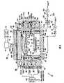
如图1所示,等离子体处理装置32具有整体上形成筒形的处理容器34,在处理容器34的内部形成有密封的处理空间S。处理容器34的侧壁以及底壁由铝等金属构成。处理容器34被电气接地。As shown in FIG. 1 , the
在处理容器34内,收容有将被处理体、例如半导体晶片W载置在其上的圆板状载置台36。载置台36能够由被进行了氧化铝处理(alumite treatment)的铝而形成。载置台36由从处理容器34的底壁立起的、由绝缘性材料而形成的支柱38支承。在载置台36中埋设有适当的加热器、例如电阻加热器40,用于加热载置在其上面的晶片W。在载置台36的上部设置有用于保持晶片W的静电卡盘(electrostaticchuck)或者夹紧(clamp)机构(未图示)。此外,载置台36也有可能与规定频率例如13.56MHz的偏置(bias)用高频电源连接。Inside the
在载置台36的上方设置有喷头44形态的气体吐出部42,用来将需要的气体喷出至该处理容器34内。在例举的实施方式中,喷头44由从平面看呈格子形排列的多个石英管而构成,石英管的排列间距为5cm左右。喷头44被安装在处理容器34的侧壁上,通过该侧壁而被支承。喷头44能够从在其下面侧形成的多个气体喷射孔44A,将成膜气体等处理气体以经控制的流量排至处理空间S。此外,喷头44的结构不局限于所述形式。A
如图2所示,在处理容器34的侧壁上设置有闸阀46,在将晶片搬入以及搬出处理容器34时该闸阀46开启。在容器底壁上设置有排气口48。在排气口48上连接有设置着压力调整阀50以及真空泵52的排气通路54,据此,根据需要,可以将处理容器34内抽真空至期望的压力。处理容器34在顶棚部具有开口,该开口通过石英或氧化铝等陶瓷材料形成的微波透过性顶板56,经由O形环等密封部件58而被气密性地闭塞。考虑到抗压性能,顶板56的厚度被设定为20mm左右。As shown in FIG. 2 , a
等离子体处理装置32具有用于在处理容器34内形成等离子体的等离子体形成单元。在本实施方式中,等离子体形成单元由将微波供给至处理容器34内的微波供给单元60而形成。微波供给单元60具有设置在顶板56上面的平面天线部件62。平面天线部件62上设置有由高介电常数材料、例如氮化铝形成的滞波件64。滞波件64根据其波长缩短的效果,将微波的管内波长缩短。平面天线部件62作为波导箱66的底板而构成,该波导箱66由覆盖滞波件64的上方整体区域的导电性中空圆筒形容器构成。平面天线部件62与处理容器34内的载置台36相对。The
波导箱66以及平面天线部件62的周边部都电气接地。同轴波导管68的外侧导体68A连接在波导箱66的上部中心部。设置在外侧导体68A内部的中心导体68B穿通滞波件64的中心贯通孔,与平面天线部件62的中心部连接。同轴波导管68经由模式变换器70、波导管72以及匹配器74与产生规定频率例如2.45GHz微波的微波发生器76连接。微波的频率不局限于2.45GHz,也可以是其他频率,例如8.35GHz。此外,作为波导管可以使用截面为圆形或矩形的波导管,或使用同轴波导管。Both the
当被处理体是8英尺大小的晶片时,可设定平面天线部件62的直径为300~400mm。在本实施方式中,平面天线部件62由厚度为1~数mm的导电性材料,例如表面镀银的铜板或铝板形成。由细长贯通孔乃至狭缝形成的多个微波放射孔62A形成在平面天线部件62上。微波放射孔62A的配置形式可以是同心圆状、漩涡状或放射状,或者也可以将其均匀分布在天线部件62整面上。When the object to be processed is an 8-foot wafer, the diameter of the
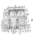
特别是如图3及图4详细所示,处理容器34由多个、此处是由三个环形金属制的块体80、82、84构成。换言之,通过沿水平面切断处理容器34而将该处理容器34分割为多个块体。块体80、82、84被沿上下方向进行层积,真空隔热层(块体间真空隔热层)86、88被设置在邻接块体间的分界部上。In particular, as shown in detail in FIGS. 3 and 4 , the
在本实施方式中,处理容器34的侧壁被分割成支承顶板56的上层块体80、支承喷头44的中层块体82、以及对应于载置台36的高度位置的下层块体84。下层块体84的下部与处理容器34的底壁90以直接金属接触的方式连接,通过未图示的金属螺栓进行结合。在下层块体84与底壁90之间设置有O形环等密封部件92。中层块体82以及下层块体84的外周面被由不锈钢等金属材料形成的保护罩部件98、100覆盖。在中层块体82以及下层块体84和保护罩部件98、100之间分别设置有外侧真空隔热层94、96。保护罩部件98、100的外侧表面上分别设置有树脂制的外罩本体98A、100A,用以提高防火的安全性。In this embodiment, the side wall of the
特别如图3所示,在邻接的块体80、82以及邻接的块体82、84之间分别设置有多个非金属制的间隔(spacer)部件102、104,用以调整邻接块体间的间隙(块体间的间隙)即真空隔热层的尺寸。间隔部件102、104具有长方体或立方体形状并沿圆周方向等间隔配置。如表示下层块体84上面的图2所示,沿圆周方向配置多个、例如四个间隔部件104。间隔部件104的数量不局限于图示的例子。间隔部件102、104为了抑制块体间的热传导,由非金属制的材料,例如低热传导性的聚酰亚胺树脂而形成。Especially as shown in FIG. 3, a plurality of non-metallic spacer (spacer)
各个块体的形状可以相异。如图2所示,下层块体84的形状从平面看为四角形。中层块体82也能够形成从平面看的八角形的形状。在图1、图3以及图4等中为了避免图面的复杂化,各个块体80、82、84均以相同的截面形状表示。The shapes of the individual blocks may vary. As shown in FIG. 2 , the shape of the
在本实施方式中,为了形成真空隔热层86、88,将沿处理容器34的周边方向延伸的相对较宽的环状凹部106、108形成在中层块体82以及下层块体84的上面。环形密封槽110、112以及114、116形成在该凹部106、108的内周侧以及外周侧上。各密封槽110、112以及114、116内分别安装有O形环等密封部件110A、112A以及114A、116A。如果相互结合块体80、82、84,则凹部106、108的内周部分以及外周部分通过密封部件110A、112A以及114A、116A被气密地密封,分别形成隔热用间隙118、120。隔热用间隙118、120部分上的块体间的间隔(gap)H1为1mm左右,隔热用间隙118、120以外部分上的块体间的间隔H2为0.2mm左右。In this embodiment, relatively wide
在中层块体82以及下层块体84的内部,贯通有排气通路121,其将隔热用间隙118以及120相互连通,并且具有在下层块体84的下面开口的出口122A。如图1所示,在排气通路121的出口122A上连接有间隙用真空排气系统124。真空排气系统124由其一端连接在出口122A上的排气通路126、依次设置在该排气通路126上的涡轮式分子泵(turbo-molecular pump)128、压力计130、压力控制阀132以及干燥泵(dry pump)134而构成。通过真空排气系统124将隔热用间隙部118、120内抽真空至规定的压力,由此,隔热用间隙118以及120作为真空隔热层86、88而起作用。此外,由于涡轮式分子泵128是用于抽高真空的泵,当不要求高真空时,能够省略涡轮式分子泵128。另外,通过增加排气通路121的数量也能够促进真空隔热层86、88间的排气速度。Inside the
再次返回到图3,在划分隔热用间隙118、120的两凹部106、108内的内周侧的局部上,形成有沿处理容器34的周边方向延伸的环状屏蔽(shield)用凹部138、140。在屏蔽用凹部138、140内设置有具有盘簧(coil spring)形态并整体呈环状的屏蔽部件142、144。各个屏蔽部件以被夹持在其上下的块体之间并在沿上下方向被弹性压坏的状态下与该上下的块体接触,确保该上下块体间的电气导通。因此,从处理空间S侧传至块体间的缝隙的微波或高频波被屏蔽部件142、144的屏蔽而不会泄漏到处理容器34的外侧。此外,在本实施方式中,各个块体80、82、84分别电气接地。Returning to FIG. 3 again, an annular shielding (shield)
并且,在内周侧的密封部件110A、114A的更内侧上,在邻接块体间的间隙中,沿处理容器34的周边方向设置有由例如树脂材料形成的防止等离子体侵入用环部件150、152,防止由于处理空间S内的等离子体等自由基(radical)到达密封部件110A、114A而产生的密封部件110A、114A的损伤。In addition, on the inside of the sealing
另外,在中层以及下层块体82、84的外周侧形成的外侧真空隔热层94、96由外侧隔热用间隙(外侧间隙)162、164构成。外侧隔热用间隙162、164,通过由O形环等密封部件154、156以及158、160分别气密性地密封在各个块体82、84的外周面和各个保护罩部件98、100之间形成的小间隙的上下两端部而进行划分。外侧隔热用间隙162、164经由连通通路166、168与所述排气通路121连通。因此,通过使与排气通路121连接的真空排气系统124运行,外侧隔热用间隙162、164也被抽真空,其结果,外侧隔热用间隙162、164作为外侧真空隔热层94、96而起作用。也可以不使隔热用间隙118、120与外侧隔热用间隙部162、164连通,而使隔热用间隙118以及120相互连通,并且使外侧隔热用间隙162以及164相互连通,使间隙118以及120和间隙162以及164与另外的真空排气系统连接。由此,例如,通过仅使隔热用空间部118、120为大气压状态,就能够在维修时将高温化的处理容器34的温度迅速降低。In addition, the outer vacuum
如图2所示,下层块体84的保护罩部件100,在容器周边方向上适当的位置上被分割成多个、例如四个,使该保护罩部件100的安装易于进行。中层块体82的保护罩部件98也优选被进行同样的分割。As shown in FIG. 2 , the
如图1所示,在上层块体80中设置有可将制冷剂流入其内部的制冷剂通路170,作为块体冷却单元。也可以使用冷却器作为块体冷却部件。在中层块体82以及下层块体84中分别设置有块体加热部件172、174。设置在中层块体82中的块体加热部件172,能够为埋设在中层块体82内并沿处理容器34的周边方向延伸的电阻加热封装加热器(sheath heater)。设置在下层块体84中的块体加热部件174能够为埋设在下层块体84内的棒状的多个筒形加热器(cartridge heater)。这些加热器的种类不局限于上述的加热器。As shown in FIG. 1 , a
为了将块体80、82、84之间相互连结,能够使用金属制的螺栓和螺母。图5是表示中层块体82与下层块体84之间的连结的示意图。将金属制的螺栓180通插入螺栓孔中,并将其用螺母182拧紧。在螺栓180以及螺母182与其座面之间存在环形垫圈184,并分别存在导热性低的耐热树脂制的环状隔板185、186,通过隔板185、186的隔热作用而抑制两块体82、84间的热传导。设定隔板185的高度为20~30mm左右,具有比另一个隔板186高的隔热作用。上层块体80与中层块体82之间的连结也能够采取同样的方法实施。In order to connect the
再次回到图1,在各个块体80、82、84上分别设置有例如热电偶188A、188B、188C,作为温度检测部件。各个热电偶188A~188C的输出被输入至由微型计算机等构成的温度控制单元190。温度控制单元190根据热电偶188A、188B、188C的输出(即各个块体的实际温度)以及各个块体的目标温度对上述块体冷却部件170以及块体加热部件172、174分别进行控制。Returning again to FIG. 1 , for example,
以下,针对采用等离子体处理装置32进行的根据等离子体CVD的成膜方法进行说明。首先,针对形成处理容器34的各个块体80、82、84的目标(设定)温度进行说明。为了抑制氧化铝制顶板56的消耗而将支承顶板56的上层块体80的设定温度定为100℃左右。为了防止在中层块体82内侧表面产生不必要的附着膜的堆积,将中层块体82的设定温度定为200℃左右。为了防止在下层块体84的内侧表面产生不必要的附着膜的堆积,将下层块体84的设定温度定在150℃~200℃范围,例如、定在150℃左右。此外,处理容器34的底壁90的温度也基本与下层块体84的温度相同。此外,使下层块体84的控制温度低于中层块体82的理由是,由于下层块体84与底壁90热接触,将其设定为不产生不必要的附着膜堆积的最低限温度。Hereinafter, a film forming method by plasma CVD using the
在成膜时,首先,经由闸阀46(参照图2)将半导体晶片W通过搬运臂(未图示)将收容在处理容器34内,通过上下移动升降销(liftpin)(未图示)而将晶片W载置在载置台36上面的载置面上。然后,通过载置台36的电阻加热器40将晶片W维持在加工温度。When forming a film, first, the semiconductor wafer W is stored in the
另外,将处理容器34内维持在规定的加工压力,例如0.01~数Pa范围内,从气体吐出部42的喷头44供给例如CF系等气体并进行流量控制。同时将通过微波发生器76而发生的微波经由波导管72以及同轴波导管68而供给至平面天线部件62,将经滞波件64而缩短波长后的微波导入处理空间S,由此,使在处理空间S内产生等离子体并进行规定的等离子体CVD处理。此时,等离子体在顶板56的正下方区域200产生,该等离子体向下方扩散并使气体活性化而产生活性种,通过该活性种的作用对晶片W的表面进行规定的等离子体CVD处理。其结果,在晶片表面形成例如氟碳膜。此时的加工温度例如晶片温度为330℃左右。In addition, the inside of the
在进行所述处理的同时,间隙用真空排气系统124被驱动并且各个真空隔热层86、88以及各个外侧真空隔热层94、96内被抽真空,同时,通过来自温度控制单元190的控制,各个块体80、82、84被分别控制成如前所述的规定温度。在进行处理时,顶板56由于在其正下方区域200形成的等离子体辐射热而被曝露于高温中,但通过支承该顶板56的上层块体80将制冷剂流入冷却通路170内,顶板56以及上层块体80被维持在100℃左右。因此,抑制了由于等离子体的顶板56的消耗,因而能够抑制伴随顶板56消耗而产生的微粒,并能够延长顶板56的寿命。Simultaneously with the processing, the
另外,中层块体82通过设置其中的块体加热部件172而被加热并被维持在200℃左右,另外,下层块体84以及与其金属性接触的底壁90通过设置在下层块体84中的块体加热部件174而被加热,被维持在例如150℃。通过将块体82、84维持相对较高的温度,能够防止不需要的碳氟膜附着在其内侧表面,另外,即使附着也能够通过干法蚀刻容易地除去。In addition, the
另外,邻接块体80、82、84之间没有直接的金属性接触,而且由于邻接块体之间设置有真空隔热层86、88,所以能够大幅度地抑制各个块体间的热传导。其结果,能够对各个块体进行分别并且有效的温度控制。另外,因为不需要如现有技术那样设置内壁,结构简单,也不需扩大装置的尺寸。In addition, there is no direct metallic contact between the
另外,由于在被维持高温状态的中层以及下层块体82、84的外周上分别经由外侧真空隔热层94、96设置有保护罩部件98、100,因而能够大幅度抑制从块体82、84向保护罩部件98、100的热传导,其结果,能够不使结构复杂化而将保护罩部件98、100的温度维持在安全温度。另外,由于能够抑制热量向外部溢出,因而能够提高加热效率。In addition, since the
另外,由于设置了防止等离子体侵入用的环部件150、152,能够防止由于从处理空间S侧侵入各个块体80、82、84间的间隙的等离子体等自由基而对密封部件110A、114A造成的损伤。另外,由于设置了密封部件142、144,能够防止由于集肤效应(skin effect)而使微波(高频波时也同样)从处理空间S一侧侵入各个块体80、82、84之间的间隙并泄漏到处理容器34的外部。In addition, since the
另外,对附着在处理容器34的内壁面上的不需要的膜进行干法蚀刻(清除)时,通过一边从喷头44流出氧化气体,例如O2气体一边产生等离子体而进行。此时,与前面说明的等离子体CVD处理时相同,使间隙用真空排气系统124以及温度控制单元190运行,将各个块体80、82、84分别维持在例如与等离子体CVD处理时的温度相同的温度。In addition, dry etching (removal) of an unnecessary film adhering to the inner wall surface of the
此处,针对各个真空隔热层86、88以及外侧真空隔热层94、96的间隔H1的最佳值进行了探讨,所以下面针对其探讨结果进行说明。图6是表示真空隔热层内的压力和间隔H1对热通量产生的影响的图表。此处,使间隔H1在1~100mm范围变化。如图表所示,如果将真空隔热层内的压力设定在10-3Torr以下,则与间隔H1的大小无关,热通量依存于压力。因此发现,从装置小型化的角度看,如果将间隔H1设定在1mm左右,优选设定在1mm以上,将真空隔热层内的压力设定在10-3Torr以下,则能够确认能获得高的隔热效果。另外,当压力在10-2~10-3Torr范围内,间隔为1mm的情况与10mm的情况下,在热通量间基本没有差。因此发现,如果使用能够将压力保持在10-2Torr以下的间隙用真空排气系统124,则只要将间隔H1设定为1mm左右,优选设定在1mm以上即可。Here, since the optimum value of the space|interval H1 of each vacuum
接着,将在两个块体之间流动的传热量针对每个部位进行了比较,以下参照表1针对比较结果进行说明。此处,为了进行比较,同时记录了采用不是真空的空气隔热层时的数值。Next, the amount of heat transfer flowing between the two blocks was compared for each site, and the comparison results will be described with reference to Table 1 below. Here, for comparison, values are also recorded when an air insulation layer other than vacuum is used.
【表1】【Table 1】
在表1中,表示Qvac表示经由1mTorr的真空隔热层流动的传热量、Qatm表示经由间隙中的空气层(外侧密封部件的外周侧)流动的传热量、Qrad表示经由放射的传热量、Qo-ring表示经由密封部件、树脂制的间隔部件、树脂制的防止等离子体侵入用环形部件而流动的传热量、Qshield表示经由金属制的屏蔽部件流动的传热量。In Table 1, Qvac represents the amount of heat transfer through a vacuum heat insulating layer of 1 mTorr, Qatm represents the amount of heat transfer through the air layer in the gap (outer peripheral side of the outer sealing member), Qrad represents the amount of heat transfer through radiation, and Qo -ring represents the heat transfer amount flowing through the sealing member, the resin spacer member, and the resin plasma penetration preventing annular member, and Qshield represents the heat transfer amount flowing through the metal shielding member.
从表1可以发现,当块体间的隔热用间隙被大气填满(空气隔热层)时,存在538W(瓦特)的传热量,与此相对,采用本发明的真空隔热层时传热量降至149W,能够将传热量降低至30%以下。并且,在采用真空隔热层的传热量中,经由真空隔热层流动的传热量Qvac的值与其他部分的传热量相比极小,因而也可以将间隔H1设定在1mm以下。It can be found from Table 1 that when the gaps between the blocks for heat insulation are filled with the atmosphere (air heat insulation layer), there is a heat transfer of 538W (Watt). The heat is reduced to 149W, which is able to reduce the heat transfer to less than 30%. In addition, in the heat transfer amount using the vacuum heat insulating layer, the value of the heat transfer amount Qvac flowing through the vacuum heat insulating layer is extremely small compared with the heat transfer amount in other parts, so the interval H1 can also be set at 1 mm or less.
另外,从表1发现,经由真空隔热层传导的传热量Qvac相对于总传热量所占的比例极小,因此,如前参照图6所示的图表进行的说明一样,即使将真空隔热层内的压力设定为10-2Torr左右也能够充分地维持隔热效果。这样,如果将到达压力设定为不那么低的压力,便可以不使用涡轮式分子泵等高真空用的泵。In addition, it is found from Table 1 that the proportion of the heat transfer Qvac conducted through the vacuum insulation layer to the total heat transfer is extremely small. Therefore, as explained above with reference to the graph shown in FIG. The heat insulation effect can be maintained sufficiently even if the pressure in the layer is set to about 10-2 Torr. In this way, if the attained pressure is set to a pressure that is not so low, it is not necessary to use a pump for high vacuum such as a turbo molecular pump.
另外,针对外侧真空隔热层94、96的效果进行研究发现,使空气进入该隔热层而呈大气压的情况时,保护罩部件98、100的表面侧的温度为78℃,与此相对,当使外侧真空隔热层94、96起作用时,保护罩部件98、100的表面侧的温度为40℃,确认能够下降38℃。In addition, studies on the effect of the outer vacuum
第一变形例First Modification
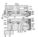
如上所述的实施方式中,中层块体82由单一的段体(piece)而构成,但如图7所示,也可以由相互层积的多个、例如三个段体82A、82B、82C构成中层块体82。此时,邻接段体(82A~82C)之间介设有O形环等密封部件202,将段体间的间隙密封,并且,使邻接段体(82A~82C)之间进行金属性接触以良好地保持段体之间的热传导性。此时,在邻接段体之间也可以设置防止微波等泄漏用的屏蔽部件。这样,通过以多个段体组合构成中层块体82,能够使各个段体分别持有特别的功能。例如,能够在上层块体82A上设置沿其内周面形成多个气体喷射口并供给清洗气的气环(gas ring)结构(参照图8)。In the embodiment described above, the
第二变形例Second Modification
在已经说明的图1及图7所示的处理装置中,例如对该处理容器34内进行维修时,将顶板56和设置在处理容器34顶棚部的上层块体80一起拆除将处理容器34开放,之后,操作者进行处理容器34内的维修作业。In the processing apparatus shown in FIGS. 1 and 7 that have been described, for example, when performing maintenance in the
但是,此时,由于喷头44被固定在中层块体82上使得维修作业非常难以进行,另外,有时不得不将喷头44拆除,使得维修操作非常麻烦。另外,当再次组合安装上层块体80时,必需进行对其与中层块体82之间的隔热用间隙的宽度进行调整的繁琐操作。But at this time, because the
此处,在本第二变形例中,能够将固定着喷头44的部分和上层块体80一起从喷头44下侧的部分分离,以便能够迅速地进行维修作业。Here, in this second modified example, the portion to which the
以下,针对第二变形例,参照图8至图10进行详细说明。此外,在图8至图10中,对于与图1以及图7中所示的构成部分相同的构成部分付与相同的编号并省略对其的说明。如参照图7已经进行的说明一样,中层块体82被分割成多个,此处是三个环状的段体82A、82B、82C。上层段体82A沿其内周面设置有多个气体喷射孔204,形成气环的结构。能够根据需要将清洗气体从气体喷射孔204供给至处理容器34内。Hereinafter, a second modified example will be described in detail with reference to FIGS. 8 to 10 . In addition, in FIGS. 8 to 10 , the same components as those shown in FIGS. 1 and 7 are denoted by the same reference numerals, and description thereof will be omitted. As already described with reference to FIG. 7 , the
中层段体82B支承喷头44。各个段体82A、82B、82C以在维修时等根据需要下层段体82C和其上面的中层段体82B能够分离的形式进行组合安装。上层块体80与上层以及中层段体82A以及82B通过未图示的螺栓被结合成一体。如上所述,图9是表示由上层块体80和上层及中层段体82A及82B构成的整体从下层段体82C分离的状态。The
对应于所述结构,外侧真空隔热层94以及保护罩98被分别分割成上下的外侧真空隔热层94X、94Y和保护罩98X、98Y,形成能够与所述分离操作对应的形式。另外同样,对应于被分离成两个的外侧真空隔热层94X、94Y,分别形成与间隙用真空排气系统124的排气通路121连通的连通通路166X、166Y。Corresponding to the above structure, the outer vacuum
另外,如图10所示,在处理容器34的侧部上设置有对上层块体80进行开关用的展开机构210。该展开机构210具有通过气缸等执行机构进行旋转的旋转轴212。将臂214从该旋转轴212延伸,将该臂214的前端与上层块体80连接固定。因此,通过使展开机构210运行,上层块体80和上层及中层段体82A、82B一体化后的一体物,如图10所示以旋转轴212为旋转中心旋转展开。In addition, as shown in FIG. 10 , an unfolding mechanism 210 for opening and closing the
由此,处理容器34的顶棚侧被开放,操作者不受喷头44的干扰可以迅速并且方便地进行维修操作。另外,当将上述一体物反向旋转进行组合安装时,只要能将分离的中层段体82B和下层段体82C密封性良好地进行接合就可以,不需要对两者间进行微妙的调整等,因而操作方便。As a result, the ceiling side of the
由于上述展开操作能够在保持上层块体80与上层及中层段体82A、82B结合为一体的状态下进行,因而不需要对隔热用间隙118进行再次调整。由此,可以迅速进行维修作业。此处,将中层块体82分割成了三块,但分割数并不局限于此。也可以将上层和中层的段体82A、82B结合成一个整体段体。此时,中层块体82被分割成两个段体。Since the above-mentioned unfolding operation can be performed while keeping the
此外,展开机构210也可适用在图1及图7的实施方式中,但是,图1的情形中,包括顶板56的上层块体80被展开。In addition, the unfolding mechanism 210 can also be applied to the embodiments of FIGS. 1 and 7 , however, in the case of FIG. 1 , the
本发明并不局限于所述实施方式以及变形例。例如,所述的各个块体80、82、84的设定温度仅为一个举例,并非局限于此。The present invention is not limited to the above-described embodiments and modifications. For example, the set temperatures of the
另外,根据块体80的设定温度,也可以在块体80上设置块体加热部件。另外,处理容器34的分割数(块体的数量)也不局限于三个。In addition, a block heating member may be provided on the
等离子体处理装置进行的处理,不局限于由等离子体CVD进行的氟碳膜的成膜处理,例如也可以是SiO2膜等其他薄膜的堆积、等离子体蚀刻处理或者等离子体灰化处理等其他等离子体处理。The processing performed by the plasma processing apparatus is not limited to the film-forming processing of the fluorocarbon film carried out by plasma CVD, and may be, for example, deposition of other thin films such asSiO2 film, plasma etching processing or plasma ashing processing, etc. plasma treatment.
在所述实施方式中,为了产生等离子体而采用了微波,但并不局限于此,例如也可以采用13.54MHz等的高频波,也可采用由磁控管的磁场和直流电场产生的磁控管振荡。即,等离子体形成单元可以作为在处理容器内形成适当强度的电场、磁场、电磁场的部件而构成。In the above-described embodiment, microwaves are used to generate plasma, but it is not limited thereto. For example, high-frequency waves such as 13.54 MHz may be used, and magnetrons generated by the magnetic field of a magnetron and a DC electric field may also be used. oscillation. That is, the plasma forming unit can be configured as a means for forming an electric field, a magnetic field, and an electromagnetic field of appropriate strength in the processing container.
在所述实施方式中,采用在处理容器34内形成等离子体的等离子体形成单元,但并不局限于此,也可采用类似所谓远程等离子体发生器这样,在处理容器34的外部生成等离子体并将该等离子体导入处理容器34内的等离子体导入单元。In the above-described embodiment, a plasma forming unit that forms plasma inside the
本发明也能够适用于不采用通过微波或高频波产生的等离子体的处理装置,例如进行热CVD处理、改性处理、以及氧化扩散处理等的情形中。此时,当然不需要防止等离子体侵入用的环形件150、152以及屏蔽部件142、144。The present invention can also be applied to a processing apparatus that does not use plasma generated by microwaves or high-frequency waves, for example, when thermal CVD processing, modification processing, and oxidation diffusion processing are performed. In this case, of course, the
另外,被处理体不局限于半导体晶片,也可以是LCD基板、玻璃基板、陶瓷基板等。In addition, the object to be processed is not limited to a semiconductor wafer, and may be an LCD substrate, a glass substrate, a ceramic substrate, or the like.
Claims (17)
Applications Claiming Priority (3)
| Application Number | Priority Date | Filing Date | Title |
|---|---|---|---|
| JP2005302592 | 2005-10-18 | ||
| JP302592/2005 | 2005-10-18 | ||
| JP171484/2006 | 2006-06-21 |
Publications (2)
| Publication Number | Publication Date |
|---|---|
| CN101061572A CN101061572A (en) | 2007-10-24 |
| CN100477091Ctrue CN100477091C (en) | 2009-04-08 |
Family
ID=38866688
Family Applications (1)
| Application Number | Title | Priority Date | Filing Date |
|---|---|---|---|
| CNB2006800011989AExpired - Fee RelatedCN100477091C (en) | 2005-10-18 | 2006-10-18 | processing device |
Country Status (1)
| Country | Link |
|---|---|
| CN (1) | CN100477091C (en) |
Families Citing this family (5)
| Publication number | Priority date | Publication date | Assignee | Title |
|---|---|---|---|---|
| JP5582819B2 (en)* | 2010-02-24 | 2014-09-03 | 東京エレクトロン株式会社 | Processing equipment |
| CN104299874B (en)* | 2013-07-17 | 2017-10-20 | 中微半导体设备(上海)有限公司 | A kind of plasma processing apparatus |
| CN103397309A (en)* | 2013-08-02 | 2013-11-20 | 光垒光电科技(上海)有限公司 | Air-inlet device and reaction chamber |
| CN109727838B (en)* | 2017-10-31 | 2021-09-17 | 北京北方华创微电子装备有限公司 | Plasma generating cavity and semiconductor processing equipment |
| CN116121708B (en)* | 2023-01-04 | 2023-09-08 | 上海欧展电器有限公司 | Heating device for be used for vacuum coating machine |
- 2006
- 2006-10-18CNCNB2006800011989Apatent/CN100477091C/ennot_activeExpired - Fee Related
Also Published As
| Publication number | Publication date |
|---|---|
| CN101061572A (en) | 2007-10-24 |
Similar Documents
| Publication | Publication Date | Title |
|---|---|---|
| TWI390605B (en) | Processing device | |
| KR101317018B1 (en) | Plasma treatment apparatus | |
| CN100388434C (en) | Substrate holding structure and plasma processing apparatus for semiconductor processing | |
| JP4230556B2 (en) | Remote microwave plasma source module | |
| JP3906203B2 (en) | Inductively coupled plasma processing equipment | |
| KR100927913B1 (en) | Substrate Mounting Mechanism and Substrate Processing Equipment | |
| WO2010038729A1 (en) | Plasma processing apparatus | |
| JP2006041539A (en) | Dual-chamber plasma processing apparatus | |
| JP5121698B2 (en) | Plasma processing equipment | |
| TWI749109B (en) | Substrate processing device and heat insulation board | |
| US20170369996A1 (en) | Plasma film-forming apparatus and substrate pedestal | |
| JP7686038B2 (en) | Substrate Processing Equipment | |
| JP4878782B2 (en) | Plasma processing apparatus and plasma processing method | |
| CN100477091C (en) | processing device | |
| KR20180133225A (en) | Plasma processing apparatus and gas shower head | |
| JP6662998B2 (en) | Plasma processing equipment | |
| KR20080080414A (en) | Plasma processing equipment | |
| JP3889280B2 (en) | Plasma processing equipment | |
| KR101768761B1 (en) | High-frequency plasma processing apparatus and high-frequency plasma processing method | |
| JP4861208B2 (en) | Substrate mounting table and substrate processing apparatus | |
| KR102047160B1 (en) | Plasma film-forming method and plasma film-forming apparatus | |
| JP2009099807A (en) | Plasma processing device | |
| US20150176125A1 (en) | Substrate processing apparatus | |
| JP4747404B2 (en) | Plasma processing equipment | |
| CN114360994A (en) | Substrate processing apparatus |
Legal Events
| Date | Code | Title | Description |
|---|---|---|---|
| C06 | Publication | ||
| PB01 | Publication | ||
| C10 | Entry into substantive examination | ||
| SE01 | Entry into force of request for substantive examination | ||
| C14 | Grant of patent or utility model | ||
| GR01 | Patent grant | ||
| CF01 | Termination of patent right due to non-payment of annual fee | Granted publication date:20090408 Termination date:20141018 | |
| EXPY | Termination of patent right or utility model |