CN100474751C - Switching power converter and system for controlling multiple switching power converters - Google Patents
Switching power converter and system for controlling multiple switching power convertersDownload PDFInfo
- Publication number
- CN100474751C CN100474751CCNB2003801084377ACN200380108437ACN100474751CCN 100474751 CCN100474751 CCN 100474751CCN B2003801084377 ACNB2003801084377 ACN B2003801084377ACN 200380108437 ACN200380108437 ACN 200380108437ACN 100474751 CCN100474751 CCN 100474751C
- Authority
- CN
- China
- Prior art keywords
- signal
- voltage
- output
- circuit
- power supply
- Prior art date
- Legal status (The legal status is an assumption and is not a legal conclusion. Google has not performed a legal analysis and makes no representation as to the accuracy of the status listed.)
- Expired - Fee Related
Links
Images


Classifications
- H—ELECTRICITY
- H02—GENERATION; CONVERSION OR DISTRIBUTION OF ELECTRIC POWER
- H02M—APPARATUS FOR CONVERSION BETWEEN AC AND AC, BETWEEN AC AND DC, OR BETWEEN DC AND DC, AND FOR USE WITH MAINS OR SIMILAR POWER SUPPLY SYSTEMS; CONVERSION OF DC OR AC INPUT POWER INTO SURGE OUTPUT POWER; CONTROL OR REGULATION THEREOF
- H02M3/00—Conversion of DC power input into DC power output
- H02M3/02—Conversion of DC power input into DC power output without intermediate conversion into AC
- H02M3/04—Conversion of DC power input into DC power output without intermediate conversion into AC by static converters
- H02M3/10—Conversion of DC power input into DC power output without intermediate conversion into AC by static converters using discharge tubes with control electrode or semiconductor devices with control electrode
- H02M3/145—Conversion of DC power input into DC power output without intermediate conversion into AC by static converters using discharge tubes with control electrode or semiconductor devices with control electrode using devices of a triode or transistor type requiring continuous application of a control signal
- H02M3/155—Conversion of DC power input into DC power output without intermediate conversion into AC by static converters using discharge tubes with control electrode or semiconductor devices with control electrode using devices of a triode or transistor type requiring continuous application of a control signal using semiconductor devices only
- H02M3/156—Conversion of DC power input into DC power output without intermediate conversion into AC by static converters using discharge tubes with control electrode or semiconductor devices with control electrode using devices of a triode or transistor type requiring continuous application of a control signal using semiconductor devices only with automatic control of output voltage or current, e.g. switching regulators
- H02M3/157—Conversion of DC power input into DC power output without intermediate conversion into AC by static converters using discharge tubes with control electrode or semiconductor devices with control electrode using devices of a triode or transistor type requiring continuous application of a control signal using semiconductor devices only with automatic control of output voltage or current, e.g. switching regulators with digital control
- G—PHYSICS
- G05—CONTROLLING; REGULATING
- G05F—SYSTEMS FOR REGULATING ELECTRIC OR MAGNETIC VARIABLES
- G05F1/00—Automatic systems in which deviations of an electric quantity from one or more predetermined values are detected at the output of the system and fed back to a device within the system to restore the detected quantity to its predetermined value or values, i.e. retroactive systems
- G05F1/10—Regulating voltage or current
- G05F1/46—Regulating voltage or current wherein the variable actually regulated by the final control device is DC
- G05F1/56—Regulating voltage or current wherein the variable actually regulated by the final control device is DC using semiconductor devices in series with the load as final control devices
- G—PHYSICS
- G05—CONTROLLING; REGULATING
- G05F—SYSTEMS FOR REGULATING ELECTRIC OR MAGNETIC VARIABLES
- G05F3/00—Non-retroactive systems for regulating electric variables by using an uncontrolled element, or an uncontrolled combination of elements, such element or such combination having self-regulating properties
- G05F3/02—Regulating voltage or current
- G05F3/08—Regulating voltage or current wherein the variable is DC
- G05F3/10—Regulating voltage or current wherein the variable is DC using uncontrolled devices with non-linear characteristics
- G05F3/16—Regulating voltage or current wherein the variable is DC using uncontrolled devices with non-linear characteristics being semiconductor devices
- G05F3/20—Regulating voltage or current wherein the variable is DC using uncontrolled devices with non-linear characteristics being semiconductor devices using diode- transistor combinations
- G05F3/26—Current mirrors
- G05F3/262—Current mirrors using field-effect transistors only
- H—ELECTRICITY
- H02—GENERATION; CONVERSION OR DISTRIBUTION OF ELECTRIC POWER
- H02M—APPARATUS FOR CONVERSION BETWEEN AC AND AC, BETWEEN AC AND DC, OR BETWEEN DC AND DC, AND FOR USE WITH MAINS OR SIMILAR POWER SUPPLY SYSTEMS; CONVERSION OF DC OR AC INPUT POWER INTO SURGE OUTPUT POWER; CONTROL OR REGULATION THEREOF
- H02M1/00—Details of apparatus for conversion
- H02M1/08—Circuits specially adapted for the generation of control voltages for semiconductor devices incorporated in static converters
- H02M1/084—Circuits specially adapted for the generation of control voltages for semiconductor devices incorporated in static converters using a control circuit common to several phases of a multi-phase system
- H02M1/0845—Circuits specially adapted for the generation of control voltages for semiconductor devices incorporated in static converters using a control circuit common to several phases of a multi-phase system digitally controlled (or with digital control)
- H—ELECTRICITY
- H02—GENERATION; CONVERSION OR DISTRIBUTION OF ELECTRIC POWER
- H02M—APPARATUS FOR CONVERSION BETWEEN AC AND AC, BETWEEN AC AND DC, OR BETWEEN DC AND DC, AND FOR USE WITH MAINS OR SIMILAR POWER SUPPLY SYSTEMS; CONVERSION OF DC OR AC INPUT POWER INTO SURGE OUTPUT POWER; CONTROL OR REGULATION THEREOF
- H02M3/00—Conversion of DC power input into DC power output
- H02M3/02—Conversion of DC power input into DC power output without intermediate conversion into AC
- H02M3/04—Conversion of DC power input into DC power output without intermediate conversion into AC by static converters
- H02M3/10—Conversion of DC power input into DC power output without intermediate conversion into AC by static converters using discharge tubes with control electrode or semiconductor devices with control electrode
- H02M3/145—Conversion of DC power input into DC power output without intermediate conversion into AC by static converters using discharge tubes with control electrode or semiconductor devices with control electrode using devices of a triode or transistor type requiring continuous application of a control signal
- H02M3/155—Conversion of DC power input into DC power output without intermediate conversion into AC by static converters using discharge tubes with control electrode or semiconductor devices with control electrode using devices of a triode or transistor type requiring continuous application of a control signal using semiconductor devices only
- H02M3/156—Conversion of DC power input into DC power output without intermediate conversion into AC by static converters using discharge tubes with control electrode or semiconductor devices with control electrode using devices of a triode or transistor type requiring continuous application of a control signal using semiconductor devices only with automatic control of output voltage or current, e.g. switching regulators
- H02M3/158—Conversion of DC power input into DC power output without intermediate conversion into AC by static converters using discharge tubes with control electrode or semiconductor devices with control electrode using devices of a triode or transistor type requiring continuous application of a control signal using semiconductor devices only with automatic control of output voltage or current, e.g. switching regulators including plural semiconductor devices as final control devices for a single load
- H02M3/1588—Conversion of DC power input into DC power output without intermediate conversion into AC by static converters using discharge tubes with control electrode or semiconductor devices with control electrode using devices of a triode or transistor type requiring continuous application of a control signal using semiconductor devices only with automatic control of output voltage or current, e.g. switching regulators including plural semiconductor devices as final control devices for a single load comprising at least one synchronous rectifier element
- H—ELECTRICITY
- H03—ELECTRONIC CIRCUITRY
- H03M—CODING; DECODING; CODE CONVERSION IN GENERAL
- H03M5/00—Conversion of the form of the representation of individual digits
- H03M5/02—Conversion to or from representation by pulses
- H03M5/04—Conversion to or from representation by pulses the pulses having two levels
- H03M5/06—Code representation, e.g. transition, for a given bit cell depending only on the information in that bit cell
- H03M5/08—Code representation by pulse width
- H—ELECTRICITY
- H05—ELECTRIC TECHNIQUES NOT OTHERWISE PROVIDED FOR
- H05B—ELECTRIC HEATING; ELECTRIC LIGHT SOURCES NOT OTHERWISE PROVIDED FOR; CIRCUIT ARRANGEMENTS FOR ELECTRIC LIGHT SOURCES, IN GENERAL
- H05B41/00—Circuit arrangements or apparatus for igniting or operating discharge lamps
- H05B41/14—Circuit arrangements
- H05B41/26—Circuit arrangements in which the lamp is fed by power derived from DC by means of a converter, e.g. by high-voltage DC
- H05B41/28—Circuit arrangements in which the lamp is fed by power derived from DC by means of a converter, e.g. by high-voltage DC using static converters
- H05B41/282—Circuit arrangements in which the lamp is fed by power derived from DC by means of a converter, e.g. by high-voltage DC using static converters with semiconductor devices
- H05B41/2825—Circuit arrangements in which the lamp is fed by power derived from DC by means of a converter, e.g. by high-voltage DC using static converters with semiconductor devices by means of a bridge converter in the final stage
- H05B41/2828—Circuit arrangements in which the lamp is fed by power derived from DC by means of a converter, e.g. by high-voltage DC using static converters with semiconductor devices by means of a bridge converter in the final stage using control circuits for the switching elements
- H—ELECTRICITY
- H02—GENERATION; CONVERSION OR DISTRIBUTION OF ELECTRIC POWER
- H02J—CIRCUIT ARRANGEMENTS OR SYSTEMS FOR SUPPLYING OR DISTRIBUTING ELECTRIC POWER; SYSTEMS FOR STORING ELECTRIC ENERGY
- H02J2207/00—Indexing scheme relating to details of circuit arrangements for charging or depolarising batteries or for supplying loads from batteries
- H02J2207/20—Charging or discharging characterised by the power electronics converter
- H—ELECTRICITY
- H02—GENERATION; CONVERSION OR DISTRIBUTION OF ELECTRIC POWER
- H02M—APPARATUS FOR CONVERSION BETWEEN AC AND AC, BETWEEN AC AND DC, OR BETWEEN DC AND DC, AND FOR USE WITH MAINS OR SIMILAR POWER SUPPLY SYSTEMS; CONVERSION OF DC OR AC INPUT POWER INTO SURGE OUTPUT POWER; CONTROL OR REGULATION THEREOF
- H02M1/00—Details of apparatus for conversion
- H02M1/0003—Details of control, feedback or regulation circuits
- H02M1/0012—Control circuits using digital or numerical techniques
- H—ELECTRICITY
- H02—GENERATION; CONVERSION OR DISTRIBUTION OF ELECTRIC POWER
- H02M—APPARATUS FOR CONVERSION BETWEEN AC AND AC, BETWEEN AC AND DC, OR BETWEEN DC AND DC, AND FOR USE WITH MAINS OR SIMILAR POWER SUPPLY SYSTEMS; CONVERSION OF DC OR AC INPUT POWER INTO SURGE OUTPUT POWER; CONTROL OR REGULATION THEREOF
- H02M1/00—Details of apparatus for conversion
- H02M1/0067—Converter structures employing plural converter units, other than for parallel operation of the units on a single load
- H02M1/007—Plural converter units in cascade
- H—ELECTRICITY
- H02—GENERATION; CONVERSION OR DISTRIBUTION OF ELECTRIC POWER
- H02M—APPARATUS FOR CONVERSION BETWEEN AC AND AC, BETWEEN AC AND DC, OR BETWEEN DC AND DC, AND FOR USE WITH MAINS OR SIMILAR POWER SUPPLY SYSTEMS; CONVERSION OF DC OR AC INPUT POWER INTO SURGE OUTPUT POWER; CONTROL OR REGULATION THEREOF
- H02M1/00—Details of apparatus for conversion
- H02M1/0067—Converter structures employing plural converter units, other than for parallel operation of the units on a single load
- H02M1/008—Plural converter units for generating at two or more independent and non-parallel outputs, e.g. systems with plural point of load switching regulators
- Y—GENERAL TAGGING OF NEW TECHNOLOGICAL DEVELOPMENTS; GENERAL TAGGING OF CROSS-SECTIONAL TECHNOLOGIES SPANNING OVER SEVERAL SECTIONS OF THE IPC; TECHNICAL SUBJECTS COVERED BY FORMER USPC CROSS-REFERENCE ART COLLECTIONS [XRACs] AND DIGESTS
- Y02—TECHNOLOGIES OR APPLICATIONS FOR MITIGATION OR ADAPTATION AGAINST CLIMATE CHANGE
- Y02B—CLIMATE CHANGE MITIGATION TECHNOLOGIES RELATED TO BUILDINGS, e.g. HOUSING, HOUSE APPLIANCES OR RELATED END-USER APPLICATIONS
- Y02B20/00—Energy efficient lighting technologies, e.g. halogen lamps or gas discharge lamps
- Y—GENERAL TAGGING OF NEW TECHNOLOGICAL DEVELOPMENTS; GENERAL TAGGING OF CROSS-SECTIONAL TECHNOLOGIES SPANNING OVER SEVERAL SECTIONS OF THE IPC; TECHNICAL SUBJECTS COVERED BY FORMER USPC CROSS-REFERENCE ART COLLECTIONS [XRACs] AND DIGESTS
- Y02—TECHNOLOGIES OR APPLICATIONS FOR MITIGATION OR ADAPTATION AGAINST CLIMATE CHANGE
- Y02B—CLIMATE CHANGE MITIGATION TECHNOLOGIES RELATED TO BUILDINGS, e.g. HOUSING, HOUSE APPLIANCES OR RELATED END-USER APPLICATIONS
- Y02B70/00—Technologies for an efficient end-user side electric power management and consumption
- Y02B70/10—Technologies improving the efficiency by using switched-mode power supplies [SMPS], i.e. efficient power electronics conversion e.g. power factor correction or reduction of losses in power supplies or efficient standby modes
Landscapes
- Engineering & Computer Science (AREA)
- Power Engineering (AREA)
- Physics & Mathematics (AREA)
- Microelectronics & Electronic Packaging (AREA)
- Radar, Positioning & Navigation (AREA)
- Electromagnetism (AREA)
- General Physics & Mathematics (AREA)
- Automation & Control Theory (AREA)
- Nonlinear Science (AREA)
- Theoretical Computer Science (AREA)
- Dc-Dc Converters (AREA)
- Details Of Television Scanning (AREA)
- Communication Control (AREA)
- Arrangements For Transmission Of Measured Signals (AREA)
- Emergency Protection Circuit Devices (AREA)
- Analogue/Digital Conversion (AREA)
Abstract
Description
Translated fromChinese技术领域technical field
本发明涉及开关电源或变换器。特别地,本发明涉及简单、耐用的开关电源,其能够为给定电路中多个不同的稳压电源提供电能。This invention relates to switching power supplies or converters. In particular, the present invention relates to simple, robust switching power supplies capable of powering a number of different regulated power supplies in a given circuit.
背景技术Background technique
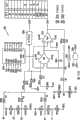
开关电源被用于在多个产品中例如蜂窝电话、照相机、PDA(个人数字助理)、计算器、便携式计算机以及类似的电子设备提供电能。这种开关电源十分复杂,并且使用大量元件以提供多个精确地调整的输出电压,以为包含在被供电的产品中的各种集成电路和其它元件提供电能。相对于使用它们的产品的成本和质量,这种电源是昂贵的、体积大并且效率低。对于为设备提供长电池寿命的功效是很重要的。图1示出了由电池10供电的在便携设备中使用的典型的现有技术的电源。来自电池10的信号通过导线10a传输到电平转换电路12,该电平转换电路被来自模拟脉冲宽度调制的控制器11的控制信号所控制。来自模拟脉冲宽度调制控制器的控制信号对导线17a和17b上的信号检测到的电阻器16两端的压降敏感,导线17a和17b分别将电阻器16的两端连接到模拟PWM控制器11。连接N沟道MOS晶体管13a和13b,以互补方式工作。电平转换电路12为N沟道晶体管13a的栅极提供高电平电压,以将来自电池10的脉冲应用于线圈15的一个输入端。线圈15的另一个输入端连接到电阻器16的一端。电阻器16的另一端连接到负载电容器18,该负载电阻器18包含为该具体的电路供电所必需的电压的充电,其中具体的电路由电源的该部分供电。模拟PWM控制器11测量通过电阻器16的电流并控制N沟道MOS晶体管13a的导通时间。N沟道MOS晶体管13b由驱动N沟道MOS晶体管13a的栅极的信号的反信号(complement)驱动,并且导通以使线圈15的输入导线接地并切断通过电阻器16提供给电源所需要的电流。图2示意性地示出了模拟脉冲宽度控制器11的内部电路。Switching power supplies are used to provide power in a variety of products such as cellular phones, cameras, PDAs (Personal Digital Assistants), calculators, portable computers, and similar electronic devices. Such switching power supplies are complex and use a large number of components to provide multiple precisely regulated output voltages to power the various integrated circuits and other components contained in the powered product. Such power supplies are expensive, bulky and inefficient relative to the cost and quality of the products in which they are used. Important for providing long battery life to devices. FIG. 1 shows a typical prior art power supply used in portable devices powered by a
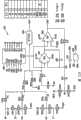
如图2所示,电流源20为电容器21提供充电电流,以生成该电容器两段的斜线电压(ramp voltage)。该斜线电压被提供给差分放大器22a的正极输入导线,其负极输入导线接收差分放大器22b的输出信号。放大器22b的正极输入导线连接到负载电容器18并传递表示负载电容器18两端电压的信号。差分放大器22b的负极输入导线连接到电阻器23a和23b之间的节点,电阻器23a和23b组成分压器(其一端连接到参考电压VREF,而另一端连接到差分放大器22b的输出导线)。这样当电容器18两端的输出电压小于电阻器23a和电阻器23b之间的节点A的电压时,差分放大器22b的输出电压转向低电平。该低电平输出电压被提供给放大器22a的负极输入导线,使放大器22a产生正的输出脉冲。该正的输出脉冲被传输到线圈15,以为电容器18提供充电电流。随着时间的增加,电容器18上的电荷增加,直到电容器18两端的电压超过节点A处的电压。在这一点上,差分放大器22b的输出电压转向高电平,以致差分放大器22a的负极输入导线上的电压超过差分放大器22a的正极输入导线上的电压,使放大器22a的输出电压变为低电平,并因此防止电容器18的进一步充电。线圈15两端的电压为负,反映电流的负的变化率,其是响应来自放大器22a的脉冲的下降沿从高电平变为低电平。由于线圈的磁场,通过线圈15的电流不会瞬间变化,但是随时间逐渐变化。这种类型的电源,其特点在于电流源驱动电容器,其被认为是模拟补偿转换器。每个MOSFET调制周期由精密比较器和误差放大器形成。这种电源难于定标和集成到集成电路中,并且典型地利用受控(captive)半导体工厂专用的模拟加工工艺制造。As shown in FIG. 2 , the
因此,需要一种能提供不同电平精度电压并同时易于用比现有技术更少的元件来实现的电源。这种电源同时必须相对便宜、耐用和可靠。Therefore, there is a need for a power supply that can provide voltages of varying levels of precision while being easy to implement with fewer components than the prior art. This power supply must at the same time be relatively cheap, durable and reliable.
发明内容Contents of the invention
根据本发明,提供了一种开关电源,其既便宜又耐用,并且同时能够提供多个不同的输出电压。According to the present invention, there is provided a switching power supply which is cheap and durable and capable of providing a plurality of different output voltages at the same time.
根据本发明的一个实施例,环形振荡器与开关矩阵一同使用,以提供一对信号,然后该对信号用于产生脉冲宽度调制信号以控制通过电感器的电流和电源中输出电容器两端的电压。来自环形振荡器被选为产生脉冲宽度调制信号的一对特殊的信号由控制器确定,该控制器检测输出电容器两端的电压并提供足够的电流以保持输出电容器两端希望的电压。输出电容器为电源驱动的电路提供选择的电压时的电流。可以控制脉冲宽度调制信号的占空比为从0到接近100%的值。环形振荡器包括奇数个反相器,反相器的数目越多,占空比越可以接近100%。相位比较器将环形振荡器的振荡频率锁定为要求的值。According to one embodiment of the invention, a ring oscillator is used with a switch matrix to provide a pair of signals which are then used to generate a pulse width modulated signal to control the current through the inductor and the voltage across the output capacitor in the power supply. The particular pair of signals from the ring oscillator selected to generate the pulse width modulated signal is determined by a controller which senses the voltage across the output capacitor and provides sufficient current to maintain the desired voltage across the output capacitor. The current at which the output capacitor supplies the selected voltage to the circuit driven by the power supply. The duty cycle of the pulse width modulated signal can be controlled from 0 to a value close to 100%. A ring oscillator includes an odd number of inverters, and the more the number of inverters, the closer the duty cycle can be to 100%. The phase comparator locks the oscillation frequency of the ring oscillator to the desired value.
在可选的实施例中,n位计数器用于产生两个信号,一个信号与另一个信号有时间偏差,从而两个信号之间的延迟控制脉冲宽度调制器输出的脉冲的宽度。在一个实施例中,该结构包括两个数字比较器,每个驱动触发电路(flip-flop),该触发电路产生由每个比较器中的时延延迟的输出信号。In an alternative embodiment, an n-bit counter is used to generate two signals, one time offset from the other such that the delay between the two signals controls the width of the pulse output by the pulse width modulator. In one embodiment, the structure includes two digital comparators, each driving a flip-flop that produces an output signal delayed by a time delay in each comparator.
本发明的电路可以控制多个不同电源的电压电平。特别地,环形振荡器上不同抽头的可用性允许选择不同对信号,每对信号用于响应相应的输出电容器上不同于要求的标称值的电压,产生单独的脉冲宽度调制信号。因此根据本发明的单个控制器可以控制系统中的多个电源,每个电源提供不同的电压。The circuit of the present invention can control the voltage levels of a plurality of different power supplies. In particular, the availability of different taps on the ring oscillator allows the selection of different pairs of signals, each for generating a separate pulse width modulated signal in response to a voltage on a corresponding output capacitor that differs from the nominal value required. Thus a single controller according to the invention can control multiple power supplies in the system, each supplying a different voltage.
本发明的脉冲宽度调制控制电路经济,便于利用商业半导体工厂可用的标准生产工艺在集成电路基片上制造,并且能够用于要求的脉冲宽度调制输出信号的多种应用中。The pulse width modulation control circuit of the present invention is economical, convenient to manufacture on integrated circuit substrates using standard manufacturing processes available in commercial semiconductor factories, and can be used in a variety of applications requiring a pulse width modulated output signal.
根据本发明的一个实施例,提供预测控制回路以调整一个或多个输出电压。该预测控制回路可以使用计算单元(例如,微控制器)以应用数字控制技术来调整输出电压。在一个实施例中,信号的占空比驱动脉冲宽度调制转换器中的开关以改变外部电感器中的电流,以响应转换器输出电压的改变。在根据本发明的一项控制技术中,利用转换器的线性电路模型,转换器预测对输出电压变化的响应(例如,当负载被接通时),并将非线性修正应用到多个时间步长上。在一个实施例中,转换器试图将其恢复到平衡状态,其中输出电压被恢复,电感器中的平均电流(“线圈电流”)是负载中的平均电流,以及线圈电流从时间步长到时间步长不发生变化。According to one embodiment of the invention, a predictive control loop is provided to regulate one or more output voltages. The predictive control loop may use a computing unit (eg, a microcontroller) to apply digital control techniques to regulate the output voltage. In one embodiment, the duty cycle of the signal drives a switch in a pulse width modulated converter to change the current in an external inductor in response to a change in the converter output voltage. In one control technique according to the invention, using a linear circuit model of the converter, the converter predicts the response to changes in the output voltage (for example, when a load is switched on) and applies nonlinear corrections to multiple time steps grow up. In one embodiment, the converter tries to bring it back to equilibrium, where the output voltage is restored, the average current in the inductor ("coil current") is the average current in the load, and the coil current varies from time step to time The step size does not change.
根据本发明,提供了一种开关电源转换器,其包括:According to the present invention, there is provided a switching power converter comprising:
环形振荡器,其由多个串联的反相器组成;a ring oscillator consisting of a plurality of inverters connected in series;
反馈环路,其连接在所述多个串联的反相器的最后一个反相器的输出导线到所述多个串联的反相器的第一个反相器的输入导线;a feedback loop connecting an output lead of a last inverter of said plurality of series-connected inverters to an input lead of a first inverter of said plurality of series-connected inverters;
选择电路,其能够从所述多个串联的反相器中的一反相器选择一个输出信号;selection circuitry capable of selecting an output signal from one of said plurality of series-connected inverters;
异或门,其在一个输入导线上接收所选择的所述输出信号,和在另一个输入导线上从所述多个串联的反相器中的一反相器的输出导线上接收参考输出信号。an exclusive OR gate receiving the selected output signal on one input lead and the reference output signal on the other input lead from the output lead of an inverter of the plurality of series-connected inverters .
根据本发明所提供的开关电源转换器,其中所述异或门可产生输出信号,该信号可具有与向所述异或门提供输入信号的反相器之间的反相器数量成比例的持续时间。According to the switching power converter provided by the present invention, wherein the exclusive OR gate can generate an output signal, which can have a ratio proportional to the number of inverters between the inverters providing the input signal to the exclusive OR gate duration.
根据本发明所提供的开关电源转换器,其中来自所述异或门的输出信号的占空比能从0变化到(n-1)/n,其中n是所述多个串联的反相器中的反相器的数量。According to the switching power converter provided by the present invention, the duty cycle of the output signal from the exclusive OR gate can be changed from 0 to (n-1)/n, where n is the plurality of inverters connected in series The number of inverters in .
根据本发明所提供的开关电源转换器,其中所述环形振荡器的振荡频率可等于1除以2nΔ,其中n是所述多个串联的反相器中的反相器的数量,而Δ是信号通过每个所述反相器的时间延迟。According to the switching power converter provided by the present invention, the oscillation frequency of the ring oscillator can be equal to 1 divided by 2nΔ, where n is the number of inverters in the plurality of series-connected inverters, and Δ is The signal is time-delayed through each of the inverters.
根据本发明所提供的开关电源转换器,其中所述环形振荡器的振荡周期可为2nΔ。According to the switching power converter provided by the present invention, the oscillation period of the ring oscillator can be 2nΔ.
本发明还提供了一种用于控制多个本发明所提供的开关电源转换器的系统,所述系统包括:The present invention also provides a system for controlling a plurality of switching power converters provided by the present invention, the system comprising:
可编程的控制电路,其被配置为接收数字信息,该数字信息识别每个所述开关电源转换器的电路布局和被所述控制电路控制的所述电源转换器的相关目标电压,该可编程的控制电路接收表示所述电源转换器电压的信息,并比较每个电源转换器相对于其各自的目标电压的电压,并响应在该电压和所述目标电压的区别的识别,执行程序以提供输出控制信号来促使脉冲宽度调制信号的产生,以修正所述开关电源转换器的工作。a programmable control circuit configured to receive digital information identifying the circuit topology of each of said switching power converters and an associated target voltage for said power converters controlled by said control circuit, the programmable The control circuit receives information representing the voltages of the power converters and compares the voltage of each power converter with respect to its respective target voltage, and in response to identification of a difference between that voltage and the target voltage, executes a program to provide A control signal is output to cause generation of a pulse width modulated signal to modify operation of the switching power converter.
本发明还提供了一种用于控制多个本发明所提供的开关电源转换器的系统,所述系统包括:The present invention also provides a system for controlling a plurality of switching power converters provided by the present invention, the system comprising:
可编程的控制电路,其被配置为接收数字信息,该数字信息识别每个所述开关电源转换器的电路布局和被所述控制电路控制的所述电源转换器的相关目标电流,该可编程的控制电路接收表示所述电源转换器电流的信息,并比较每个电源转换器相对于其各自的目标电流的电流,并响应在该电流和所述目标电流的区别的识别,执行程序以提供输出控制信号来促使脉冲宽度调制信号的产生,以修正所述开关电源转换器的工作。a programmable control circuit configured to receive digital information identifying the circuit topology of each of said switching power converters and an associated target current for said power converters controlled by said control circuit, the programmable The control circuit receives information representing the current of the power converters and compares the current of each power converter with respect to its respective target current, and in response to identification of a difference between the current and the target current, executes a program to provide A control signal is output to cause generation of a pulse width modulated signal to modify operation of the switching power converter.
本发明还提供了一种用于多个控制本发明所提供的开关电源转换器的系统,所述系统包括:The present invention also provides a system for controlling multiple switching power converters provided by the present invention, the system comprising:
可编程的控制电路,其被配置为接收数字信息,该数字信息识别每个所述开关电源转换器的电路布局和被所述控制电路控制的所述电源转换器的相关目标电功率,该可编程的控制电路接收表示所述电源转换器电功率的信息,并比较每个电源转换器相对于其各自的目标电功率的电功率,并响应在该电功率和所述目标电功率的区别的识别,执行程序以提供输出控制信号来促使脉冲宽度调制信号的产生,以修正所述开关电源转换器的工作。a programmable control circuit configured to receive digital information identifying the circuit topology of each of said switching power converters and the associated target electrical power of said power converters controlled by said control circuit, the programmable The control circuit receives information representing the electrical power of the power converters and compares the electrical power of each power converter relative to its respective target electrical power, and in response to identification of a difference between the electrical power and the target electrical power, executes a program to provide A control signal is output to cause generation of a pulse width modulated signal to modify operation of the switching power converter.
根据本发明所提供的系统,其可进一步包括According to the system provided by the present invention, it may further include
采样和保持电路,其连接到每个所述开关电源转换器并对来自每个被控制的所述开关电源转换器的数据进行采样;a sample and hold circuit connected to each of said switching power converters and sampling data from each of said switching power converters being controlled;
以及包括and include
模数转换电路,其连接到所述采样和保持电路的输出,并且其输出连接到所述可编程控制电路。an analog-to-digital conversion circuit connected to the output of the sample and hold circuit, and the output of which is connected to the programmable control circuit.
根据本发明所提供的系统,可进一步包括The system provided according to the present invention may further include
数字脉冲控制电路,其连接到所述可编程控制电路的输出,该数字脉冲控制电路响应从所述可编程控制电路接收的信息,产生数字信号以控制所述多个开关电源转换器的工作。A digital pulse control circuit coupled to the output of the programmable control circuit, the digital pulse control circuit responsive to information received from the programmable control circuit, generates digital signals to control the operation of the plurality of switching power converters.
结合与下面详细描述一起说明的附图,将更充分地理解本发明。The present invention will be more fully understood in conjunction with the accompanying drawings that accompany the following detailed description.
附图说明Description of drawings
图1表示现有技术中模拟降压变换器的基本结构;Fig. 1 shows the basic structure of analog buck converter in the prior art;
图2表示图1中模拟PWM控制器11的详细结构;Fig. 2 shows the detailed structure of
图3表示根据本发明的使用环形振荡器的脉冲宽度调制控制器的基本结构;Figure 3 shows the basic structure of a pulse width modulation controller using a ring oscillator according to the present invention;
图4表示根据本发明的脉冲宽度调制控制器的可选的实施方案;Figure 4 shows an alternative embodiment of a pulse width modulation controller according to the invention;
图5表示使用图3的结构产生的波形的例子;Figure 5 shows an example of a waveform generated using the structure of Figure 3;
图6表示根据本发明使用的环形振荡器和用于从环形振荡器中选择特定的输出信号的开关矩阵,该输出信号被提供给异或门63的两条输入导线,以生成脉冲宽度调制的信号;Figure 6 shows a ring oscillator used in accordance with the present invention and a switch matrix for selecting a particular output signal from the ring oscillator which is supplied to the two input leads of an exclusive OR
图7表示利用图6的结构产生的信号的波形;Figure 7 shows the waveform of a signal generated using the structure of Figure 6;
图8表示利用图6的结构产生的波形,其中在图6中,在环形振荡器的每个偶数反相器的输出引线和由信号G,H,I,J及K驱动的旁路晶体管之间连接反相器;Figure 8 shows the waveforms produced using the structure of Figure 6, where in Figure 6, between the output lead of each even inverter of the ring oscillator and the pass transistors driven by signals G, H, I, J, and K Connect the inverter between;
图9表示当从图6的环形振荡器中的反相器对的不同组合选择信号时,得到的相对延时;Figure 9 shows the relative delays obtained when signals are selected from different combinations of inverter pairs in the ring oscillator of Figure 6;
图10表示用于控制对特定门的选择,以将选择的一对信号传输到图6中的异或门63,以产生脉冲宽度调制信号的电路;FIG. 10 shows a circuit for controlling the selection of a specific gate to transmit the selected pair of signals to the exclusive OR
图11表示根据本发明的原理,从图6中的异或门63产生脉冲宽度调制信号的另一个电路;Fig. 11 shows another circuit for generating a pulse width modulated signal from exclusive OR
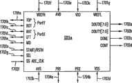
图12是根据本发明一个实施例的开关电源控制器1200的框图;FIG. 12 is a block diagram of a switching
图13是根据一个实施方案的表示数字脉冲变换器封装(wrapper)1201的接口信号的框图;13 is a block diagram representing interface signals of a digital pulse converter package (wrapper) 1201, according to one embodiment;
图14是根据一个实施方案的表示模数转换器1206的接口信号的框图;Figure 14 is a block diagram representing the interface signals of the analog-to-
图15是表示Kelvin温度传感器(KTS)1500的接口信号的框图;Figure 15 is a block diagram representing the interface signals of a Kelvin temperature sensor (KTS) 1500;
图15A是根据一个实施例的用于KTS 1500的示例性电路;Figure 15A is an exemplary circuit for a
图16是说明QSADC模块1211a进行的四重斜率(quad-slope)(即,双重变换)模数转换(ADC)操作的时序图,该模块包含在触摸屏接口1211中;16 is a timing diagram illustrating the quad-slope (i.e., double conversion) analog-to-digital conversion (ADC) operation performed by the
图17是表示在一个实施方案中QSADC模块1211a的接口信号的框图;Figure 17 is a block diagram representing the interface signals of the
图17A是表示在一个实施方案中触摸屏接口1211中的QSADC模块1211a的接口信号的框图;Figure 17A is a block diagram representing the interface signals of the
图18是根据本发明的一个实施例的QSADC模块1211a的俯视框图,包括模拟模块ANLG1801、控制模块CNTRL1802,以及DOWN/UP计数器模块1803;Fig. 18 is a top block diagram of a
图18A表示图18所示的QSADC模块1211a的模拟模块1801的一个实施方案;Figure 18 A shows an embodiment of the
图18B表示四点(four-contact)触摸屏应用的一种排列;Figure 18B shows an arrangement for four-contact touch screen applications;
图18C表示五点(five-contact)触摸屏应用的一种排列;Figure 18C shows an arrangement for five-contact touch screen applications;
图19是概括开关电源控制器1200中的模块的框图,其为电池和电源管理应用提供控制回路;FIG. 19 is a block diagram outlining the modules in a switching
图20说明根据本发明的一个实施例的利用电感器电流IL调整输出电压Vout,和感应输出电压Vout;FIG. 20 illustrates adjusting the output voltage Vout using the inductor currentIL and sensing the output voltage Vout according to one embodiment of the present invention;
图21说明由占空比加权平均的电感器电流的近似值;Figure 21 illustrates an approximation of the inductor current weighted by the duty cycle;
图22说明本发明用于估计MOS开关的寄生电阻的方法;Figure 22 illustrates the method of the present invention for estimating the parasitic resistance of a MOS switch;
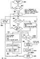
图23表示流程图2300,说明根据本发明一个实施例的控制方法;Figure 23 shows a
图24说明根据本发明一个实施例的低频闭环和高频开环的控制方法;Fig. 24 illustrates the control method of the low-frequency closed-loop and high-frequency open-loop according to one embodiment of the present invention;
图25是表示开关电源控制器1200用于电池和电源管理(例如,在用于个人数字助理(PDA)应用的方框图;FIG. 25 is a block diagram showing a switching
图26说明根据本发明的控制回路的操作;Figure 26 illustrates the operation of the control loop according to the present invention;
图27根据本发明的一个实施例,说明图24的低频闭环和高频开环控制方法,表示受控变量的特征(singature)输入值和开环响应;Fig. 27 illustrates the low-frequency closed-loop and high-frequency open-loop control methods of Fig. 24 according to one embodiment of the present invention, showing the characteristic (singature) input value and open-loop response of the controlled variable;
图28根据本发明的一个实施例,说明连续的瞬态恢复控制方法;Figure 28 illustrates a continuous transient recovery control method according to one embodiment of the present invention;
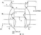
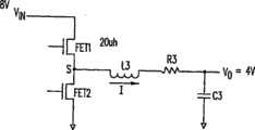
图29说明降压转换器;Figure 29 illustrates a buck converter;
图30到图33表示根据不同门电路驱动电压应用到晶体管时,对于例如电路49的电源电路关于时间的电流曲线;Figures 30 to 33 show current curves with respect to time for a power supply circuit such as
图34是表示时钟发生器1223的接口信号的框图;FIG. 34 is a block diagram representing interface signals of the
图35表示图34和图12所示的时钟发生器模块的端口表格;Figure 35 represents the port table of the clock generator module shown in Figure 34 and Figure 12;
图36表示示例性的脉冲宽度调制实施方案,其包括脉冲宽度发生器和序列发生器,用于数字脉冲转换器1201;FIG. 36 shows an exemplary pulse width modulation implementation including a pulse width generator and a sequencer for
图36A是图36的脉冲宽度发生器的示例性实施方案;Figure 36A is an exemplary embodiment of the pulse width generator of Figure 36;
图36B是图36的序列发生器的示例性实施方案;Figure 36B is an exemplary embodiment of the sequencer of Figure 36;
图36C表示示例性的反馈控制系统;Figure 36C shows an exemplary feedback control system;
图36D表示另一个示例性的反馈控制系统;Figure 36D shows another exemplary feedback control system;
图37表示根据一个实施方案的用于DPC1201的数字脉冲转换器一帧的时序图;FIG. 37 shows a timing diagram for one frame of the digital pulse converter for DPC1201 according to one embodiment;
图37A表示一个实施方案的数字脉冲转换器1201的示例性接口信号;Figure 37 A represents the exemplary interface signal of
图37B说明DPC1201的示例性电路实施方案,其包括CAM;Figure 37B illustrates an exemplary circuit implementation of
图37C说明用于图37B的CAM的一个示例性实施方案;Figure 37C illustrates an exemplary embodiment for the CAM of Figure 37B;
图37D说明用于图37C中CAM的输出逻辑的示例性电路实施方案;Figure 37D illustrates an exemplary circuit implementation for the output logic of the CAM in Figure 37C;
图37E说明用于图37C的CAM的示例性时序图;Figure 37E illustrates an exemplary timing diagram for the CAM of Figure 37C;
图38表示Grey计数器的示例性实施方案;Figure 38 shows an exemplary implementation of a Gray counter;
图38A表示Grey计数器的另一个示例性实施方案;Figure 38A shows another exemplary embodiment of a Gray counter;
图38B表示图38或图38A的触发器的示例性实施方案;Figure 38B represents an exemplary embodiment of the flip-flop of Figure 38 or Figure 38A;
图38C表示图38或图38A的另一个触发器的示例性实施方案;FIG. 38C represents an exemplary embodiment of another flip-flop of FIG. 38 or FIG. 38A;
图38D表示用于逻辑门的示例性电路实施方案;Figure 38D shows an exemplary circuit implementation for logic gates;
图38E表示用于另一个逻辑门的示例性电路实施方案;Figure 38E shows an exemplary circuit implementation for another logic gate;
图38F表示多路复用器的示例性电路实施方案;Figure 38F shows an exemplary circuit implementation of a multiplexer;
图38G表示二进制到Grey以及Grey到二进制转换的示例性电路实施方案;Figure 38G shows an exemplary circuit implementation for binary to Gray and Gray to binary conversion;
图38H说明数字脉冲转换器的示例性实施方案;Figure 38H illustrates an exemplary implementation of a digital pulse converter;
图38I说明数字脉冲转换器的另一个示例性实施方案;Figure 38I illustrates another exemplary embodiment of a digital pulse converter;
图39表示典型的门电路驱动波形的曲线图,其可以被用于,例如,电路49中晶体管的门电路和S端的产生的电压;Figure 39 shows a graph of typical gate drive waveforms that may be used, for example, for the gate and S terminal voltages of transistors in
图40是一个实施方案中SHM1207的框图;Figure 40 is a block diagram of SHM1207 in one embodiment;
图40A是说明用于一个实施方案的电压和电流采样的功能原理图;Figure 40A is a functional schematic illustrating voltage and current sampling for one embodiment;
图40B是说明用于一个实施方案的电压和电流选择的电路示意图;Figure 40B is a circuit schematic illustrating voltage and current selection for one embodiment;
图40C是根据另一个实施方案的用于SHM1207的示例性接口信号模块;Figure 40C is an exemplary interface signal module for SHM1207 according to another embodiment;
图40D是另一个实施方案中的SHM1207的框图;Figure 40D is a block diagram of SHM1207 in another embodiment;
图40E是说明用于另一个实施方案的电压和电流采样的功能原理图;Figure 40E is a functional schematic diagram illustrating voltage and current sampling for another embodiment;
图40F是说明用于另一个实施方案的电压和电流选择的电路示意图;Figure 40F is a circuit schematic illustrating voltage and current selection for another embodiment;
图40G是根据另一个实施方案的时钟发生电路;Figure 40G is a clock generation circuit according to another embodiment;
图40H是根据另一个实施方案的分压器;Figure 40H is a voltage divider according to another embodiment;
图40I是根据另一个实施方案的电压放大器;Figure 401 is a voltage amplifier according to another embodiment;
图40J是根据另一个实施方案的用于输入输出电路的示例性接口信号模块;Figure 40J is an exemplary interface signal module for an input output circuit according to another embodiment;
图40K是根据另一个实施方案的多路复用器方案;Figure 40K is a multiplexer scheme according to another embodiment;
图41是根据本发明一个实施例的图12的调节控制模块(REG)的框图;Figure 41 is a block diagram of the regulation control module (REG) of Figure 12 according to one embodiment of the invention;
图42表示相对于时间的门电路驱动波形;Figure 42 shows gate drive waveforms versus time;
图42A表示升压转换器电路;Figure 42A shows a boost converter circuit;
图42B表示时间上偏移的两个开关波形;Figure 42B shows two switching waveforms shifted in time;
图43表示说明电流的波形A,B和C,其中的电流为开关电源的三个门电路驱动情况的输出;Figure 43 shows waveforms A, B and C illustrating the currents as the output of the three gate drives of the switching power supply;
图43A表示端点S上的电压相对于时间的曲线图,端点S位于图29的降压转换器49中上部和下部晶体管之间;FIG. 43A shows a graph of voltage versus time at terminal S between the upper and lower transistors in
图43B和图43C表示端点S加电压的曲线图,用于电路49中FET50的两个不同占空比;Figures 43B and 43C represent graphs of voltage applied to terminal S for two different duty cycles of
图44表示用于生产高电压以驱动冷阴极荧光灯泡的电路;Figure 44 shows a circuit for producing high voltage to drive a cold cathode fluorescent bulb;
图44A表示两组示例性门电路驱动波形,其可以被用于电路1.2.2.12的晶体管的门电路;Figure 44A shows two sets of exemplary gate drive waveforms that may be used for the gates of the transistors of circuit 1.2.2.12;
图45表示降压转换器电路;Figure 45 shows a buck converter circuit;
图45A表示用于图45中晶体管的门电路驱动波形,和相应的电流和输出电压波形;Figure 45A shows the gate drive waveforms for the transistor in Figure 45, and the corresponding current and output voltage waveforms;
图45B表示升压电路;Figure 45B shows a boost circuit;
图45C表示用于图45B的电路的门电路驱动波形,和相应的电流和输出电压波形;Figure 45C shows gate drive waveforms for the circuit of Figure 45B, and corresponding current and output voltage waveforms;
图46表示调节两个开关电源的操作所连接的开关电源控制器1200;Figure 46 shows a switching
图46A表示相对于时间的在开关电源的一个周期的电流曲线图;FIG. 46A shows a graph of current over one cycle of a switching power supply versus time;
图46B表示降压电源电路;Figure 46B shows a step-down power supply circuit;
图46C表示相对于时间的在开关电源电路的一个周期的电流曲线图;FIG. 46C shows a graph of current in one cycle of a switching power supply circuit versus time;
图46D表示相对于时间的在开关电源的一个周期的电流曲线图;Figure 46D shows a graph of current over one cycle of a switching power supply versus time;
图46E表示相对于时间的用于开关电源电路的电流曲线图;Figure 46E shows a graph of current versus time for a switching power supply circuit;
图47表示连接到多个电源的开关电源控制器1200;Figure 47 shows a switching
图48以框图的形式表示连接到两个开关电源的处理器,非易失性存储器和Kelvin温度传感器,电池连接到开关电源之一上;Figure 48 represents in block diagram form a processor connected to two switching power supplies, a non-volatile memory and a Kelvin temperature sensor, and a battery connected to one of the switching power supplies;
图48A表示对于典型的电池的电池容量与温度的曲线;Figure 48A shows a graph of battery capacity versus temperature for a typical battery;
图49表示与蜂窝电话共同使用的电源系统的框图;Figure 49 shows a block diagram of a power system for use with a cellular telephone;
图49A表示连接到电源的太阳能电池阵列的框图,该电源由本发明的开关电源控制器1200控制;Figure 49A shows a block diagram of a solar cell array connected to a power source controlled by a switching
图50是根据本发明的一个实施例的扩频分频器单元2482.4的框图;Figure 50 is a block diagram of a spread spectrum divider unit 2482.4 according to one embodiment of the present invention;
图50A是根据本发明的一个实施例用于图50中扩频分配器单元2482.4的频谱扩频器210.1的电路图;Figure 50A is a circuit diagram of spectrum spreader 210.1 for spread spectrum divider unit 2482.4 of Figure 50 according to one embodiment of the present invention;
图51是表示另一个实施方案中QSADC模块1211b的接口信号的框图;Figure 51 is a block diagram representing the interface signals of the
图51A是根据本发明的另一个实施例的QSADC模块1211b的俯视框图,其包括模拟模块2001.4、控制模块2002.4、以及up/down计数器模块2003.4;51A is a top block diagram of a
图51B表示图51A模拟模块2001.4的一个实施方案;Figure 51B shows an embodiment of the analog module 2001.4 of Figure 51A;
图51C说明表示触摸屏接口1211和开关电源控制器1200的其它模块之间的示例性接口信号的框图;51C illustrates a block diagram representing exemplary interface signals between
图51D表示执行QSADC模块1211a的诊断的流程图;FIG. 51D shows a flowchart for performing diagnostics of the
图51E表示相应于图51B的实施方案的功能性框图;Figure 51E represents a functional block diagram corresponding to the embodiment of Figure 51B;
图51F说明用于初始测量状态的模拟模块1801的电路连接;FIG. 51F illustrates the circuit connections of the
图51G说明由于与四触点实施方案中Y坐标薄片的连接的模拟模块1801的电路连接以对电压积分;Fig. 51G illustrates the circuit connection of the
图51H说明由于与四触点实施方案中Y坐标薄片的连接的模拟模块1801的电路连接以数字地转换该电压;Figure 51H illustrates the circuit connection of the
图51I说明由于与四触点实施方案中X坐标薄片的连接的模拟模块1801的电路连接以对电压积分;Figure 51I illustrates the circuit connections of the
图51J说明由于与四触点实施方案中X坐标薄片的连接的模拟模块1801的电路连接以数字地转换该电压;Figure 51J illustrates the circuit connection of the
图51K说明模拟模块1801对电压积分的电路连接,由于与五触点实施方案中X—Y坐标薄片水平位置的连接;Fig. 51K illustrates the circuit connection of the
图51L说明模拟模块1801数字地转换电压的电路连接,由于与五触点实施方案中X—Y坐标薄片垂直位置的连接;Figure 51L illustrates the circuit connections for
图51M说明模拟模块1801对电压积分的电路连接,由于与五触点实施方案中X—Y薄片坐标水平位置的连接;Figure 51M illustrates the circuit connections of the
图51N说明模拟模块1801数字地转换电压的电路连接,由于与五触点实施方案中X—Y坐标薄片水平位置的连接;Figure 51N illustrates the circuit connections for
图51O说明模拟模块1801的电路连接,检测四触点实施方案中电阻片间的连续性;Fig. 510 illustrates the circuit connections of the
图51P说明对五点实施方案中接触的检测;Figure 51P illustrates the detection of contacts in the five-point embodiment;
图52说明LED控制模块1214的框图;FIG. 52 illustrates a block diagram of the
图53是根据本发明的一个实施例的图12中的监视定时器模块的框图;Figure 53 is a block diagram of the watchdog timer module in Figure 12 according to one embodiment of the invention;
图54是根据一个实施方案的内部电压电源(IVS)1209的示例性功能图;Figure 54 is an exemplary functional diagram of an internal voltage supply (IVS) 1209, according to one embodiment;
图54A是根据另一个实施方案的IVS1209的示例性接口框图;Figure 54A is an exemplary interface block diagram of the
图54B是根据另一个实施方案的IVS1209的另一个示例性接口框图;Figure 54B is another exemplary interface block diagram of
图54C是根据另一个实施方案的IVS1209的加电顺序的示例性流程图;Figure 54C is an exemplary flowchart of the power-up sequence of the
图55是根据一个实施方案的NFET驱动器模块1202的示例性功能图;Figure 55 is an exemplary functional diagram of an NFET driver module 1202 according to one embodiment;
图55A说明根据另一个实施方案的NFET驱动器模块1202的示例性接口信号;FIG. 55A illustrates exemplary interface signals of the NFET driver module 1202 according to another embodiment;
图55B说明根据另一个实施方案的NFET驱动器模块1202的示例性接口信号;Figure 55B illustrates exemplary interface signals of the NFET driver module 1202 according to another embodiment;
图55C表示图55B的实施方案的示例性功能图;Figure 55C represents an exemplary functional diagram of the embodiment of Figure 55B;
图55D说明对图55B的实施方案利用内部缓冲器直接驱动外部线圈的应用;Figure 55D illustrates the application of the embodiment of Figure 55B to directly drive an external coil with an internal buffer;
图55E说明对图55B的实施方案利用内部缓冲器驱动外部FET的应用;Figure 55E illustrates the application of the implementation of Figure 55B to drive an external FET with an internal buffer;
图55F表示图55B的实施方案的示例性芯片内配置的框图;Figure 55F represents a block diagram of an exemplary on-chip configuration of the embodiment of Figure 55B;
图56是根据本发明的一个实施例的图12的中央处理模块(SYS)1205的框图;Figure 56 is a block diagram of the central processing module (SYS) 1205 of Figure 12 according to one embodiment of the present invention;
图57表示图25的转换器2570的电路模块;Figure 57 shows the circuit modules of the converter 2570 of Figure 25;
图58是根据本发明的一个实施例的说明控制算法5800步骤的流程图;Figure 58 is a flowchart illustrating the steps of a control algorithm 5800 according to one embodiment of the invention;
图59说明图58的控制算法5800的操作。FIG. 59 illustrates the operation of the control algorithm 5800 of FIG. 58 .
具体实施方式Detailed ways
以下详细的描述旨在说明这里讨论的实施例,并不是用于限制本发明的范围。考虑到这个公开,本发明的其它实施例对于本领域技术人员是显而易见的。The following detailed description is intended to illustrate the embodiments discussed herein and is not intended to limit the scope of the invention. In view of this disclosure, other embodiments of the invention will be apparent to those skilled in the art.
1.0 部分,具有同步采样多路输出控制器的转换器(数字平衡多阶段SPS)的结构概述,每个模块的功能描述Section 1.0, a structural overview of a converter with simultaneous sampling multiple output controller (digital balanced multi-stage SPS), a functional description of each module
本发明应用于电能转换器和集成一组电源管理相关功能的电源管理外围设备。开关电源控制器1200(以框图的形式表示在图12中)描述了根据本发明的一个实施例的开关电源转换器控制器产品的实施方案。该系统基本上实现了电源转换器所有预期的功能,例如保持稳定的输出电压(稳压电源),该电压完全独立于从电源得到的电流;或保持稳定的输出电流(恒流电源),该电流完全独立于应用到电源上的负载;确定何时切断负载,并测量电池中的充电状态,给电池充电,以及执行电池排序(sequencing)。此外,该系统执行多个其它外围管理功能,例如数字化触摸板、扫描键盘、以及调整从系统其它部位收到的复位信号。在一个实施例中,提供监视器计时器功能以允许电力循环并向产品的不同子系统提供复位信号,响应异常条件,例如软件加锁或者甚至硬件加锁(例如,SCR锁定或由于输入输出瞬变的中断)。本发明的系统也控制显示各种子系统状态的LED。因此,根据本发明的系统当PDA的处理器断电时可以处理便携电子设备(例如,PDA)执行的很多功能,例如在笔划之间(当用户在PDA上书写注释时),或当PDA显示信息但并不是预期输入或输出时。在该实施方案中,该产品包括控制各种数字接口的数字控制子系统,该数字接口包括复位信号、监视器计时器、使能信号、用于显示内部电源各个状态的状态信号。通过通信接口提供系统中元件间的通信。在一个实施例中,本发明包括时基发生电路和到键盘的数字化仪接口。The invention is applied to power converters and power management peripherals integrating a set of power management related functions. Switching power supply controller 1200 (represented in block diagram form in FIG. 12 ) depicts an implementation of a switching power converter controller product in accordance with one embodiment of the present invention. The system basically realizes all the expected functions of the power converter, such as maintaining a stable output voltage (regulated power supply), which is completely independent of the current drawn from the power supply; or maintaining a stable output current (constant current power supply), the The current is completely independent of the load applied to the power supply; determining when to cut the load, and measuring the state of charge in the battery, charging the battery, and performing battery sequencing. In addition, the system performs several other peripheral management functions, such as digitizing the touchpad, scanning the keyboard, and adjusting reset signals received from other parts of the system. In one embodiment, a watchdog timer function is provided to allow power cycling and provide reset signals to the different subsystems of the product in response to abnormal conditions such as software lock-ups or even hardware lock-ups (for example, SCR lock-up or due to input-output transients). change interruption). The system of the present invention also controls LEDs that display the status of various subsystems. Thus, the system according to the present invention can handle many functions performed by a portable electronic device (e.g., a PDA) when the PDA's processor is powered off, such as between strokes (when the user writes notes on the PDA), or when the PDA displays information but not intended input or output. In this embodiment, the product includes a digital control subsystem that controls various digital interfaces including reset signals, watchdog timers, enable signals, status signals to indicate the various states of the internal power supply. Communication between elements in the system is provided through communication interfaces. In one embodiment, the invention includes a time base generation circuit and a digitizer interface to a keyboard.
参考图12,实际上所有数字接口功能由内部8051或可比较的微处理器执行,该微处理器被包括在中央处理模块(SYS)1205中,其与外部系统利用多个接口通过多个通用输入/输出(GPIO)信号来通信,这些信号可以在微处理器的软件中限定,并灵活地映射到各个输入或输出管脚或集成电路的接线端。例如,每个管脚可以被限定为带有高的真信号或低的真信号,并且可以被限定为输入信号或输出信号。此外,每个管脚可以被分配给单个的电源元件中的任何一个,并且可以被共享,从而多个电源可以从一个管脚收到相同的控制信号。这样,例如,单个使能信号可以被多个电源共享。该GPIO信号可以被用于实现一些外围设备的输入和输出信号。例如,键盘扫描器功能通过GPIO信号与外部键盘交互。监视器计时器可以从集成电路外部的电路接收输入信号和状态信息。同时,中断信号可以与GPIO信号共享管脚。因此该实施方案提供一组很多的功能,以允许该产品能够与基于分离的离散设备的现有技术解决方案“插接兼容”。中央处理模块(SYS)1205处理芯片上和芯片外的串行通信。能够作为GPIO信号实施方案的每个信号,除了中断信号,也可以作为串行通信信号。在为现有技术设备设计的应用中,串行通信可以被用于访问键盘和库仑定量测量能力。该GPIO信号可以被用于开启和关断单个电源,并监视它们的状态。Referring to FIG. 12, virtually all digital interface functions are performed by an internal 8051 or comparable microprocessor included in the central processing module (SYS) 1205, which interfaces with external systems through multiple general-purpose These signals can be defined in the microprocessor's software and mapped flexibly to individual input or output pins or terminals of the integrated circuit. For example, each pin may be defined as having a true high signal or a true low signal, and may be defined as an input signal or an output signal. In addition, each pin can be assigned to any one of the individual power supply elements and can be shared so that multiple power supplies can receive the same control signal from a single pin. Thus, for example, a single enable signal can be shared by multiple power supplies. The GPIO signal can be used to implement input and output signals of some peripheral devices. For example, the keyboard scanner function interacts with an external keyboard through GPIO signals. A watchdog timer can receive input signals and status information from circuits external to the integrated circuit. At the same time, interrupt signals can share pins with GPIO signals. This embodiment therefore provides a large set of functions to allow the product to be "plug compatible" with prior art solutions based on separate discrete devices. Central processing module (SYS) 1205 handles on-chip and off-chip serial communications. Every signal that can be implemented as a GPIO signal, except interrupt signals, can also be used as a serial communication signal. In applications designed for prior art devices, serial communications can be used to access the keypad and coulometric measurement capabilities. This GPIO signal can be used to turn on and off individual power supplies and monitor their status.
计算电路(其可以被提供为超长指令字处理器(“VLIW引擎”)以简化解码逻辑)被包括在调节控制模块(REG)1204中(在图12中被标记为“REG”)。VLIW引擎执行来自中央处理模块(SYS)1205(在图12中被标记为“SYS”)的低级命令。调节控制模块(REG)1204接收并解释来自稳压电源管脚供电的各种电路的电压和电流的测量。使用多个不同类型的控制环路,调节控制模块(REG)1204以精确调制的信号的形式向数字脉冲转换器(DPC)提供命令,其接着被用于通过NFET驱动器模块1202操作外部组件。开关电源控制器1200与外部组件一起构成各种指定集成电路布局的一个或多个电源转换器。Computational circuitry (which may be provided as a very long instruction word processor ("VLIW engine") to simplify decoding logic) is included in the regulation control module (REG) 1204 (labeled "REG" in FIG. 12). The VLIW engine executes low-level commands from a central processing module (SYS) 1205 (labeled "SYS" in Figure 12). A regulation control module (REG) 1204 receives and interprets voltage and current measurements from various circuits powered by the regulated supply pins. Using a number of different types of control loops, the regulation control module (REG) 1204 provides commands in the form of precisely modulated signals to the digital pulse converter (DPC), which are then used to operate external components through the NFET driver module 1202 . Switching
根据本发明该系统的一个独特的特点在于该系统是可编程的。除了允许每个功能外,模式和预先设置的调节参数、外部组件的说明可以被存储在集成电路内部,并用于执行调节器功能。因此,调节控制模块(REG)1204根据大量信息来操作,这些信息是关于开关电源控制器1200外部的电源转换器组件的特征。与现有技术的以模拟技术实施的开关电源控制器电路不同,本发明的电源控制器电路“知道”其试图获得的输出电压(“目标电压”)和误差(即,当前输出电压和目标电压之差)。特别地,现有技术的模拟转换器利用不依赖于当前开关占空比和输入电压值的算法来修正误差。这种现有技术的转换器也不在内部存储关于外部组件的信息。试图设计具有这种现有技术的电源转换器控制电路的工程师只能以补偿网络的形式向电源控制器电路提供“暗示”。与此相反,根据本发明的电源控制器电路比现有技术具有很多优点和好处。例如,由于具有关于当前输出电压和占空比的信息,目标电压和内部存储的外部电路的参数值允许电源控制器计算将导致高精度的正确的输出电压的可能的占空比,并选择遵循外部电路的约束(例如,电感器的饱和电流)的实际的响应。对外部电路异常的适当的响应限制了反射到电源控制器电路的噪声的量。例如,通过控制通过电源控制器电路的瞬时噪声电流,将电源电压提供给电源控制器电路的电池或长导线可以受到并可能辐射更少的电磁干扰(EMI)。A unique feature of the system according to the invention is that the system is programmable. In addition to allowing each function, modes and preset adjustment parameters, instructions for external components can be stored inside the integrated circuit and used to perform the regulator function. Thus, the regulation control module (REG) 1204 operates based on a large amount of information about the characteristics of the power converter components external to the switching
可编程的键盘扫描功能在中央处理模块(SYS)1205中实现,在按键被按下以从待机状态唤醒键盘扫描电路后,允许扫描或检测单个按键。监视器功能由中央处理模块(SYS)1205中的软件执行,并提供全功能的监视器定时器功能。监视器定时器功能可以被用于处理系统中的软件故障。例如运行复杂操作系统(例如,Win CE)的外部处理器可以周期性地暂时地维持(“切换”)指定管脚上的信号。无论何时指定管脚上的信号被切换,监视器定时器复位其定数器。当主机微处理器的软件发生故障时,以致指定管脚上的信号在预定时间内没有切换,那么执行一组预定程序的动作以恢复外部系统处理器的运行。这些动作包括简单地复位处理器或另一个电路元件,或使处理器的电源循环断开和接通。冷开机(power-cycling)消除了来自寄生SCR的电流,其可能出现在处理器或其它集成电路中,从而影响从半导体锁定状态中的恢复。通过冷开机也可以修正通常利用逻辑或复位信号不能恢复的其它异常。A programmable key scan function is implemented in the central processing module (SYS) 1205 and allows scanning or detection of individual keys after the key is pressed to wake up the key scan circuit from standby. The watchdog function is performed by software in the central processing module (SYS) 1205 and provides a full-featured watchdog timer function. The watchdog timer function can be used to handle software faults in the system. For example, an external processor running a complex operating system (eg, Win CE) may periodically and temporarily assert ("toggle") a signal on a specified pin. Whenever the signal on the specified pin is toggled, the watchdog timer resets its counter. When the software of the host microprocessor fails so that the signal on the designated pin does not toggle within a predetermined time, a predetermined set of programmed actions are performed to restore operation of the external system processor. These actions include simply resetting the processor or another circuit element, or cycling power to the processor off and on. Cold power-cycling removes current from parasitic SCRs, which may occur in processors or other integrated circuits, affecting recovery from semiconductor lock-up. Other anomalies that cannot normally be recovered with logic or reset signals can also be corrected by cold booting.
中央处理器模块(SYS)1205控制外部状态LED,或单个多色LED。包括在内部电压电源1209中的内部复位逻辑提供接通电源复位,以允许在操作之前稳定内部时钟和内部产生的电压。这是与下面描述的复位调节特点不同的概念,其在软件中实现,并在内部微控制器上运行。主机复位调节软件利用电源的状态信号来调节外部系统的复位信号以及产品输入管脚的外部信号。Central processing module (SYS) 1205 controls the external status LED, or a single multi-color LED. Internal reset logic included in the
触摸屏接口1211使用双斜率技术(dual-slope technique)来读取电阻式触摸板显示器的X和Y坐标。在PDA中,由于显示器的区域很大,该数字化操作容易受到背光引起的噪声影响。在现有技术中,典型的背光是由冷阴极荧光灯(CCFL)实现的,其本质上是没有阴极加热器的荧光灯泡,该阴极加热器增加用于在低电压电离的内部气体的能量。在CCFL中,对于典型的设备,初始电离(“触发”)是利用700伏或更大的交流电压产生的,并且其后使用大于300伏的交流电压保持触发。驱动CCFL的高压交流波形是潜在的对触摸板的严重的噪声源,其由电阻性材料的面板组成,被直接放置于显示器前的几毫米处。触摸屏接口1211使用四重斜率(quad-slope)模数转换器电路,该电路与电源控制器产生的背光电压同步操作。通过与背光同步地操作,来自背光的噪声在偶数周期中被积分,从而有效地被消除,而不需复杂的滤波或算法方案。The
内部电压电源1209是用于开关电源控制器1200的电源,或者来自两个外部供电管脚之一,或者来自两个外部电池管脚之一,提供各种模块运行需要的内部电压,这些模块包括中央处理模块(SYS)1205和调节控制模块(REG)1204。除了提供各种子系统需要的各种电压,内部电压电源1209还提供晶振功能(不同于晶体,其是离线的(off-chip)),用于建立内部电源的各种电荷泵,和指示电源何时稳定以适于被内部处理元件使用的比较器。The
采样和保持模块1207包括采样阵列、保持电路和扫描电路。采样和保持模块1207监视电源输出部分内的各个点,测量电压和电流,输入电压和各个点处的温度。采样和保持模块1207将其数据、每个时刻的采样提供给模数转换器1206(系统共享的资源),其将外部模拟采样转换为数字采样。数字采样被调节控制模块(REG)1204使用,或向上传递到中央处理模块(SYS)1205。在本发明的该实施例中,模数转换器和采样和保持结构或者基于电容器系数或者基于单位增益。因此,使用单个标准可以实现校准。The sample and
NFET驱动器模块1202包括一组以一个或两个模式运行的输出驱动器。第一个模式是驱动外部电源MOSFET设备。在该模式中,每个输出电压与两组驱动器电路关联;一个用于驱动控制FET,而另一个用于驱动同步FET。对于小量(modest)电流,两个驱动器电路可以用在另一个一起被驱动的运行模式中,并且他们的输出信号可以被连接在一起,以电源转换功能直接驱动外部线圈。NFET driver module 1202 includes a set of output drivers that operate in one or two modes. The first mode is to drive an external power MOSFET device. In this mode, each output voltage is associated with two sets of driver circuits; one to drive the control FET and the other to drive the sync FET. For modest currents, the two driver circuits can be used in an operating mode where the other is driven together, and their output signals can be connected together to directly drive an external coil with a power conversion function.
利用本发明的电源可以是完全可编程的,即,不需选择外部分立元件来设置电压和电流,而单个芯片可以执行在多个不同产品的多个不同的功能。这种可编程性具有减小电路板上元件数量的优点。它同时具有减少终端产品的单个生产商库存的部件数量,这是由于该相同的设备可以被用于多个不同的应用。所有这些特点可以被预先设置,或者在生产芯片的时候,或者在送出芯片的时候,即,通过销售商,利用类似于同可编程逻辑阵列设备使用的编程方法。可选地,本发明的系统可以由客户编程,甚至在其产品的电路内测试阶段或最终阶段在电路板上编程。此外,即使所有这些功能可以被编程,生产和测试期间编程的值仅被当作初始状态,并且可能被包括电源控制器的系统动态地改变(即,在运行中)。例如,系统可以动态地重新编程内部电压和电流,如需要不同电压用于不同运行模式的复杂微处理器通常需要的。为了使显示器变暗和控制发动机,也可以进行重新编程操作。数模转换功能可以通过快速改变调节器的输出电压来实现。开关电源控制器1200的特点是完全可编程的启动和关闭序列,以允许使用电源控制器1200的系统以可以避免锁定状态的序列启动。例如,微处理器的输入/输出(I/O)结构经常需要在微处理器内核之前被供电。反向该次序可能导致微处理器的损害和破坏,或导致故障。为了给这些设备断电,也需要特定的供电序列。在现有技术的解决方案中,该时序被电阻器和电容器相当简单地设置,或者根本不设置。A power supply utilizing the present invention can be fully programmable, ie, no external discrete components need to be selected to set the voltage and current, and a single chip can perform multiple different functions across multiple different products. This programmability has the advantage of reducing the number of components on the board. It also has the ability to reduce the number of components in stock of a single manufacturer of the end product, since the same device can be used for a number of different applications. All of these features can be preset, either at the time the chip is produced, or at the time the chip is shipped, ie, by the vendor, using programming methods similar to those used with programmable logic array devices. Alternatively, the system of the present invention can be programmed by the customer, even on the circuit board during the in-circuit test phase or final phase of their product. Furthermore, even though all of these functions can be programmed, the values programmed during production and testing are only considered initial states and may be changed dynamically (ie, on the fly) by the system including the power supply controller. For example, the system can dynamically reprogram internal voltages and currents, as is often required for complex microprocessors that require different voltages for different modes of operation. Reprogramming operations are also available for dimming the displays and controlling the engines. The digital-to-analog conversion function can be realized by rapidly changing the output voltage of the regulator. The switching
开关电源控制器1200控制的各个电源可以为多种集成电路布局编程,因此可以提供高于输入源、低于输入源、或有时等于输入源的电压。例如,升压转换器集成电路布局用于输出电压高于输入电压的电源,降压转换器集成电路布局用于输出电压低于输入电压的电源,单端初级电感转换器(sepic)集成电路布局用于输入和输出电压相同的电源。当需要非常高的电压时(即,冷阴极荧光灯泡或者甚至数字照相机中的照相闪光灯),可以使用例如半桥式的集成电路布局。所有这些可以被编程并且它们的任何数量可以在任何时间出现在设计中,并且可以同时支持这些集成电路布局的任何组合。The individual power supplies controlled by switching
本发明的开关电源控制器1200也可以利用脉冲宽度调制实现亮度降低。这个能力对于冷阴极荧光灯是重要的,这是因为典型地,电流的简单的降低为电离整个显示器提供不充分的能量,导致所谓的“温度计效应(thermometereffect)”,其中只有部分背光被实际上照亮。需要PWM实现亮度降低的另一个应用是在白色LED中。由于电流的作用,白色LED会有颜色或色彩上从审美角度不可接收的改变。对于亮度降低的白色LED使用脉冲宽度调制,在导通时间保持恒定的电流,因此在大的亮度降低范围内保持不变的颜色。开关电源控制器1200同时具有用在温度补偿中的输入管脚,包括:内部温度传感器,和用于读取外部温度传感器的外部管脚。温度补充用在电池充电中,以调整充电速率,以响应不稳定的环境条件,检测故障条件,和防止外部电池的破坏或由于内部过热的损坏。内部电池充电器的算法适应于多个不同的化学组成(例如,锂离子)。由于在中央处理模块(SYS)1205中执行的软件中提供多个电池充电算法,所以可以适应于任何化学组成。The switching
开关电源控制器1200也允许在不同电池之间选择来作为其电源。中央处理模块(SYS)1205可以被编程为首先使用外部电池,因而保留其内部电池用于紧急情况或当更换外部电池时。它也可以自动地选择以首先为内部电池充电,接着外部辅助电池。中央处理模块(SYS)1205计算可以得到多少能量并同时为两个电池充电,或并列地使用它们。使用本发明的产品提供的另一个功能是向外部系统提供电压、电流和电量数据的能力。这允许在达到各个极限值之前,对电压调节器功能的独立地直接控制和对电池中可获得的能量数量的中间读取。拥有本发明的系统同时保持充电接收历史记录。这在确定电池是否可能被完全充电是非常有用的。它也是电池损耗的初期指示,并且提供了限制过度充电情况的基础,在过度充电中,由于一些故障电池可能被无限地充电。Switching
根据本发明的一个方面,该产品的各个开关波形被认真地交错排列,使得从外部电源,例如电池,获得的能量的数量被尽可能地均匀分配在需要电源的所有不同输出周围。这就有效地增加了从外部电源需要的电流的频率,并可以减小来自外部电源需要的峰值电流,其降低了该外部电源上的噪声数量,同时也降低从内部连线辐射到外部电源的噪声,并使噪声易于被过滤。而且,将扩频的方法用于内部频率。这就降低了在给定频率的来自外部开关电源作用的净(net)能量。也就是说,不是总工作在固定的频率,扩频的特点允许转换频率快速地变化和使用产业标准模式调制的频率,以使在任何具体频率的能量被降低。扩频的特点有效地降低了由相关无线设备(associatedradio)将受到的噪声,该无线设备在使用本发明的产品中,或者在使用该芯片的最终产品或邻近的其它产品中。该工作频率也可以由外部源来确定。在一个实施例中,32KHz的晶振产生所有内部时钟,并提供基于32KHz的供系统内其它元件使用的输出。根据另一个特点,系统提供外部时钟,其保证距离最近的转换边缘20ns。该独特的特点允许外部系统与开关电源功能同步地进行采样,与系统同步地采样以降低内部开关噪声的方式相同。由于通常现有技术的开关电源不知道其将在给定周期中提供什么占空比,因此这种开关电源正常开关不能无法提取时间之前的信息。由于在本发明中所使用的所有脉冲宽度调制器是数字式的,通过另一个控制信号可以实施方案,该信号安排在组成所有脉冲宽度调制器的控制信号阵列中。According to one aspect of the invention, the individual switching waveforms of the product are carefully interleaved so that the amount of energy available from an external source, such as a battery, is distributed as evenly as possible around all the different outputs requiring power. This effectively increases the frequency of the current required from the external power supply and can reduce the peak current required from the external power supply, which reduces the amount of noise on that external power supply while also reducing the amount of noise radiated from the internal wiring to the external power supply noise, and make it easy to filter the noise. Also, a spread spectrum method is used for internal frequencies. This reduces the net energy at a given frequency from the action of the external switching power supply. That is, instead of always operating at a fixed frequency, the spread spectrum feature allows switching frequencies to be changed rapidly and modulated frequencies using industry standard patterns so that the energy at any particular frequency is reduced. The spread spectrum feature effectively reduces the noise that will be experienced by associated radios in the product using the invention, or in the end product or other products in the vicinity of the chip. The operating frequency can also be determined by an external source. In one embodiment, a 32KHz crystal oscillator generates all internal clocks and provides 32KHz based outputs for use by other components within the system. According to another feature, the system provides an external clock that is guaranteed to be 20 ns from the nearest transition edge. This unique feature allows the external system to sample synchronously with the switching power supply function in the same way that the system samples synchronously to reduce internal switching noise. Since typically a prior art switching power supply does not know what duty cycle it will deliver in a given cycle, such a switching power supply cannot extract information from time to time before it switches normally. Since all the pulse width modulators used in the present invention are digital, it can be implemented by means of another control signal arranged in the control signal array making up all the pulse width modulators.
参考图12,时钟发生器模块1223(CLKGEN)产生图12中所述模块需要的时钟信号。在表示接口信号的图34的高电平框图中更详细地说明时钟发生器模块1223。时钟发生器产生基于由数字脉冲控制模块1201提供的源时钟信号的时钟。该源时钟脉冲被时钟发生器模块1223分别在CST[9:0]输出总线1223.2和分别设置在接口1223.4和1223.1上的DPC 1201的输出端口PLOCK和PLLCK接收。在下表中,描述了CST总线1223.2上信号的频率。Referring to FIG. 12 , the clock generator module 1223 (CLKGEN) generates clock signals required by the modules described in FIG. 12 . The
参考到时钟发生器1223的各个接口,来自DPC模块1201的CST接口由图34的参考标记1223.2表示的10位总线组成。该总线连接到DPC1201中GREY计数器的输出,并为时钟发生器1223提供大多数源时钟。表102A表示总线CST[0]到CST[9]中每条线路上信号的频率。With reference to the respective interfaces to the
表102AForm 102A
参考标记1223.3表示的两位总线PD_OUT[1:0]控制产生的时钟信号的工作模式。电源的工作模式被指定为标准的、低功率和关机。下表102B表示在两位总线上的信号表示的模式。The two-bit bus PD_OUT[1:0] denoted by reference numeral 1223.3 controls the operating mode of the generated clock signal. The operating modes of the power supply are specified as standard, low power, and shutdown. Table 102B below shows the modes represented by the signals on the two-bit bus.
表102BForm 102B
在线路1223.7上提供到模数转换器1206的时钟信号,在下表102C中说明不同模式下的频率。低功率和标准模式下的频率来自538,870.921KHz的DPLL时钟通过5分频后的频率。The clock signal to the analog-to-
表102CForm 102C
在线路1223.9上提供采样和保持块1207的时钟信号。下表102D表示不同工作模式需要的频率。标准模式下的频率来自于比特CST[4],而低功率模式下的频率来自于CST[8]的二分频。The clock signal for sample and hold
表102DForm 102D
在线路1223.8上提供到内部电压电源1209的时钟信号,下表102E表示各种工作模式所需要的频率。标准模式下的频率来自于CST[4],即,低功率模式下的频率来自于CST[8]的二分频。The clock signal to the
表102EForm 102E
QSADC_CLK提供触摸屏接口1211的时钟信号。下表102F表示不同工作模式需要的频率。低功率和标准模式下的频率来自于CST[8]的二分频。QSADC_CLK provides a clock signal for the
表102FForm 102F
时钟发生器1223为调节控制模块(REG)1204提供标准、低功率和关机模式下的时钟信号,下表102G表示每种模式下的频率。各种模式的频率来自于,例如标准模式使用CST[0]位,低功率模式的工作频率来自于CST[8]的四分频。此外,CLKGEN 1223向调节控制模块(REG)1204提供SHM CLK和SYS CLK时钟信号。
表102GForm 102G
表102H说明用于提供给中央处理模块(SYS)1205的时钟信号的模式和用于这些模式的频率。如表102H所示,在关机模式中,频率为0。对于低功率和标准模式,频率与来自于CST[2]的频率相同。Table 102H illustrates the modes used for the clock signal provided to central processing module (SYS) 1205 and the frequencies used for these modes. As shown in Table 102H, in shutdown mode, the frequency is zero. For low power and standard modes, the frequencies are the same as those from CST [2].
表102HForm 102H
LED_CLK是用于LED模块的时钟,LED模块与中央处理模块(SYS)1205关联。下表102I表示用于不同模式的频率。标准模式下的频率来自于CST[8]的二分频。LED_CLK is the clock for the LED module, which is associated with the central processing module (SYS) 1205 . Table 102I below indicates the frequencies used for the different modes. The frequency in standard mode comes from the 2nd frequency division of CST[8].
表102IForm 102I
通过连接到中心数字电源的VDD向时钟发生器模块1223提供3.3V±300mV的数字电源电压。类似地,在线路1223.6上提供VSS,且VSS是中心数字地。A digital power supply voltage of 3.3V±300mV is provided to the
转到图35所示的端口表,无论该端口为输入或输出端口,都示出了端口名称、说明、这些端口上信号的源地址和目标地址。Turning to the port table shown in Figure 35, whether the port is an input or output port, the port name, description, source and destination addresses of the signals on those ports are shown.
参考图12所示,复位电路1221产生用于开关电源控制器1200的复位。该由电路接收和产生的信号显示在模块中。如图12所示的其它电路,接近信号名的箭头表示信号是由复位电路1221产生或被复位电路1221接收。Referring to FIG. 12 , the
1.1 部分,DPC及其操作、可选实施方案的详细描述Section 1.1, DPC and its operation, detailed description of alternative implementations
数字脉冲转换器封装1201可以作为常规混合信号电路(DPC)的组合和数字胶合逻辑(digital glue logic)的接口封装实现,数字胶合逻辑由以硬件描述语言(HDL)表示的逻辑电路描述合成。在该实施方案中,数字脉冲转换器封装1201将10位的数字值转换为具有边缘分辨约为2ns的脉冲。如下面进一步的详细解释,提供具有单个写端口和单个读端口的双端口存储器模块,以存储10位的值,该值表示脉冲开始和宽度控制、周期跳步和旁路电路控制(用于直接输出控制)。The digital
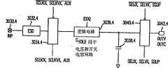
图13是根据一个实施方案的表示数字脉冲转换器封装1201的接口信号的方块图。如图13所示,数字脉冲转换器封装1201有5个接口:(a)时序控制接口1301,(b)调节控制接口1302,(c)功率调节接口1303,(d)采样和保持控制接口1304,以及(e)电源接口1305。Figure 13 is a block diagram representing the interface signals of the digital
时序控制接口1301包括频率为32KHz,占空比为50%的参考时钟信号1301a(FREF),参考时钟旁路控制信号1301b(BYPASS),数字锁相状态信号1301c(PLOCK),计时状态总线1301d(CS[9:0]),以及输出状态总线1301e(STATE[15:0]),这些接口用于为电路外部数字脉冲转换器封装1201提供时钟和控制状态。在该实施方案中,参考时钟信号1301a(即,信号FREF)是提供给数字脉冲转换器封装1201中的数字锁相环(DPLL)用于频率合成的参考时钟,而旁路控制信号1301b(即,BYPASS信号)是用于旁路DPLL的测试控制信号。PLOCK是表示DPLL中的参考时钟信号1301a的锁相状态的状态信号。计时状态总线1301d(即,总线CS[9:0])是10位的时钟状态总线,其提供时钟和控制状态以同步DPC、接口和开关电源控制器1200的其它中心电路。当计时状态总线1301d共同地显示DPC的时间状态时,计时状态总线1301d的每一位可以被用作占空比为50%的时钟。例如,如果使用31.25KHz的参考时钟,则位CS[9]相应于占空比为50%频率为256KHz的时钟,位CS[8]相应于占空比为50%频率为512KHz的时钟。通常,CS[n]相应于占空比为50%频率为f(n,m)=2-(n+m)f0的时钟,其中n ε{0,1,...,9}和mε{0,1,...,6}。输出状态总线1301e(即,总线STATE[15:0])是16位状态总线,其显示开关控制总线1303a和1303b(下述)在通过直接控制逻辑之前的内部状态,直接控制逻辑被调节控制接口1303用于限制开关控制总线1303a(即,HIGHFET)和开关控制总线1303b(即,LOWFET)的输出信号到指定的状态。总线1301e在写操作时发生信号到DPC核心电路(corecircuit)。The timing control interface 1301 includes a frequency of 32KHz, a
调节控制接口1302,提供对数字脉冲转换器封装1201中双端口存储器的存取,其包括存储器写数据总线1302a(DWI[9:0]),存储器地址总线1302b(ADW[7:0]),存储器读数据总线1302c(DWO[9:0]),写使能信号1302d(WE)以及读使能信号1302e(RE)。调节控制接口1302控制偏移和脉冲宽度用于电源调节接口1303中的各种脉冲。Adjustment control interface 1302, which provides access to dual-port memory in digital
电源调节接口1303包括开关控制总线1303a(HIGHFET[6:0])和开关控制总线1303b(LOWFET[6:0])。采样和保持控制接口1304,其通过用于系统控制环路中的ADC控制用于数字转换的模拟电压的采样和保持,该接口1304包括第一采样控制总线1304a(SMPA[6:0]),第二采样控制总线1304b(SMPB[6:0]),以及辅助控制总线1304c(SMPAX[3:0])。采样总线1304a和1304b中每一位的时序与相应的开关总线1303a或开关总线1303b中的每一位相关联。每个采样总线1304a和1304b控制用于数字转换的与HIGHFET或者与LOWFET控制总线关联的模拟电压的采样和保持。该采样控制总线1304c(即,辅助采样SMPAX[3:0])控制系统监视和控制需要的其它模拟信号的采样。The power regulation interface 1303 includes a
电源接口1305包括数字电源参考1305c(VDD),模拟电源参考1305d(AVD),数字地参考1305a(VSS)以及模拟地参考1305b(AVS)。数字电源和数字地参考信号(即,VDD和VSS参考)是全局信号。在该实施方案中,VDD是连接到中心数字电源的数字高电压电源(3.3V±10%)。AVD是连接到中心模拟电源的模拟高电压电源(3.3V±10%)。VSS和AVS分别是连接到中心数字地参考的数字地参考和模拟地参考(0V)。The power interface 1305 includes a
1.1.1 部分,PWM定时信号发生器的第一个实施例Section 1.1.1, First Embodiment of PWM Timing Signal Generator
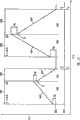
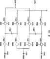
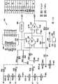
图3表示根据本发明的电源管理控制器。如图3所示,环形振荡器包括串行连接的反相器301-1到301-15。在本发明的实际的实施例中,环形振荡器可以包括多个串行连接的反相器。例如,可以串行连接一千个反相器,结果是本发明控制器得到的占空比几乎为100%。然而,为了便于解释,在该详细描述中,将只说明15个反相器。每个反相器固有地具有延迟“Δ”,其是信号输入反相器的输入导线的时间和每个反相器输出导线上获得的最后输出信号的时间之间经过的时间。该时间“Δ”是施加到包括在反相器中的组件的电压的函数。通过改变用于反相器的组件上的电压,可以改变与反相器关联的实际延迟时间Δ。CMOS技术中典型的反相器将包括电压源和参考电压之间的与N沟道MOS设备连接的P沟道MOS设备系列,其中参考电压通常是系统地。如果与反相器共同使用缓存器,可以使用额外4个晶体管,使每个反相器具有6个晶体管。与信号通过反相器的传输关联的延迟是应用到反相器的电压的函数。用于反相器的电源电压越高,信号从输入端到输出端的传输就越慢,且延迟Δ越大。Figure 3 shows a power management controller according to the present invention. As shown in FIG. 3, the ring oscillator includes serially connected inverters 301-1 to 301-15. In a practical embodiment of the invention, the ring oscillator may comprise a plurality of inverters connected in series. For example, a thousand inverters can be connected in series, resulting in a duty cycle of almost 100% obtained by the controller of the present invention. However, for convenience of explanation, in this detailed description, only 15 inverters will be explained. Each inverter inherently has a delay "Δ", which is the time elapsed between the time a signal is input to the input lead of the inverter and the time the last output signal is obtained on the output lead of each inverter. This time "Δ" is a function of the voltage applied to the components included in the inverter. By changing the voltage on the components used for the inverter, the actual delay time Δ associated with the inverter can be changed. A typical inverter in CMOS technology will consist of a series of P-channel MOS devices connected to an N-channel MOS device between a voltage source and a reference voltage, usually system ground. If the buffer is used with the inverters, an additional 4 transistors can be used, making each
在图3的结构中,能够在32.768KHz振荡的晶体302被导线303a和303b连接到反相放大器304。放大器304提供晶体两端的电压,以使晶体振荡在32.768KHz频率,从而使来自反相放大器304的输出信号振荡于晶体302的频率。环形振荡器的输出信号被八分频电路3058分频,然后送到相位比较器306,相位比较器306还接收来自振荡器302的输出信号。因此环形振荡器的控制频率是262.144KHZ,为晶体302正常频率的8倍。In the structure of FIG. 3, a
环形振荡器的正常工作频率通常被选为大约262KHz。相位比较器306检测环形振荡器输出信号8分频的信号相位和晶体振荡器302的信号相位间的相位差。相位比较器306将线路306a的输出信号中的相位差提供给Vcc控制电路307,以修正环形振荡器的输出信号8分频的频率和与晶体振荡器302的控制频率32.768KHz之间的任何偏差。如果环形振荡器频率太低,那么驱动Vcc控制电路307,以在线路307a上为反相器301-15提供更高的电压,从而减小与该反相器相关的延迟时间,并因此增加环形振荡器的振荡频率。可选地,如果环形振荡器的工作频率太高,那么Vcc控制电路307在输出线路307a上提供低输出电压,从而增加通过反相器301-15的延迟时间,并因此减小与该反相器相关的电压。The normal operating frequency of the ring oscillator is usually chosen to be around 262KHz. The
相位选择器308控制来自异或门309的输出线路310上的脉冲宽度调制(PWM)输出信号的宽度。连接到异或门309的两个输入线的每一个被相位选择器308连接到与环形振荡器中反相器301-i的一个输出线相关的接头。偶数反相器301的输出导线每次可以与一个异或门309的输入导线309a相连。奇数反相器301的输出导线每次可以与一个异或门309的输入导线309b相连。根据异或门309的输出线310上的PWM信号驱动的电源的要求,选择连接到异或门309的输入导线309a和309b的反相器301-1到301-15的特定输出导线。
无论异或门309的输入是否不同,其将具有高输出。每次高的边沿或低的边沿传输通过环形振荡器,通过异或门连接的反相器时,这种情况都会发生。由于环形振荡器的一个周期包括上升沿和下降沿,异或门309的输出导线310检测到的PWM信号频率将是环形振荡器频率的两倍。Regardless of whether the inputs to
环形振荡器(由反相器301-1到301-15组成)的正常频率“f”由与每个反相器关联的延迟时间“Δ”给定。因此如果所有反相器具有相同的延迟,那么正常频率f=1/(2nΔ),其中n是反相器的个数,Δ是与每个反相器相关的延迟时间。因此频率与反相器的个数成反比。环形振荡器的周期由1/f给定。因此,如果反相器的个数等于1000,并且与每个反相器相关的延迟为10-9秒,那么频率为500KHz,周期为2毫秒。The normal frequency "f" of the ring oscillator (consisting of inverters 301-1 to 301-15) is given by the delay time "Δ" associated with each inverter. So if all inverters have the same delay, then the normal frequency f=1/(2n[Delta]), where n is the number of inverters and [Delta] is the delay time associated with each inverter. Therefore the frequency is inversely proportional to the number of inverters. The period of the ring oscillator is given by 1/f. Thus, if the number of inverters is equal to 1000, and the delay associated with each inverter is 10-9 seconds, then the frequency is 500 KHz and the period is 2 milliseconds.
系统能够达到的不同脉冲宽度由反相器输出线路上的接头确定,这些接头连接到异或门309的输入导线309a和309b。The different pulse widths achievable by the system are determined by the connectors on the output lines of the inverters, which are connected to the input leads 309a and 309b of the
1.1.2 部分,PWM定时发生器的第二个实施例Section 1.1.2, Second Embodiment of PWM Timing Generator
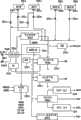
图4表示使用计数器和比较器以产生脉冲宽度调制信号的本发明的可选的实施例。5位的计数器41(如果需要,可以使用不同的位数)从0到31计数,其由16.7772MHz的信号驱动。5位计数器41的瞬时计数值通过5位总线42发送到比较器43a和43b,每个比较器将计数值和存储在其中的值比较。数字比较器43a将存储由相位选择总线44a上的信号确定的数值,且数字比较器43b将存储由相位选择总线44b上的信号确定的第二个数值。相位选择总线44a和相位选择总线44b上的信号被外部电路确定,其测量负载电容器上的电压和进入负载电容器的电流,并将该电压和电流与参考值比较,以确定负载电容器必须充电到的程度。这可以由开关电源控制器1200实现,特别是使用采样和保持电路1207、模数转换器1206以及调节控制模块(REG)1204。下面详细描述这些电路及其操作和系统的操作。数字比较器43a的输出信号切换D触发器45a,而数字比较器43b的输出信号切换D触发器45b。来自D触发器45a的反转输出信号在导线47a上传输到延迟线48a的输入导线。延迟线具有由位4-0确定的长度,以相应于驱动5位计数器为指定值使用的时间,该指定值使数字比较器43a翻转触发器45a。延迟线的输出信号在导线49a上传输到异或门49的一条输入导线。Figure 4 shows an alternative embodiment of the invention using counters and comparators to generate pulse width modulated signals. A 5-bit counter 41 (a different number of bits can be used if desired) counts from 0 to 31, driven by a 16.7772 MHz signal. The instantaneous count value of the 5-
5位计数器41在找到数字比较器43a中的匹配后继续计数,直到在数字比较器43b中找到另一个匹配。数字比较器43b中计数的特定值由来自下述相位选择—红色总线44b的位9-5设置。这种匹配导致输入信号从数字比较器43b发送到D触发器45b。然后D触发器45b在导线47b上产生输出信号,其被传输到延迟线48b的输入导线。然后,延迟线48b在导线49b上产生高电平输出信号到异或门49。在延迟线48a的输出信号为高和在延迟线48b的输出信号为低的时间期间,将由异或门49将在输出导线49c上产生脉冲宽度调制的信号。然而,当输出导线49a和49b上的输出信号电平相同时,异或门49将在输出导线49c上生成低电平输出信号。因此异或门49的输出信号是相位调制的,分别相应于相位选择—绿色总线和相位选择—红色总线44a和44b上的信号。The 5-
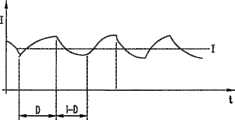
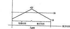
选择16.7772MHz以驱动5位计数器41,使其每秒循环完整的计数524,287.5次。换句话说,图4电路中导线49c上信号的输出频率是262,144KHz。图5说明13个串行连接的反相器的波形。顶部曲线表示到第一个反相器的输入信号。第二条曲线表示从第二个反相器输出的信号。第三条曲线表示第四个反相器输出的信号,而第五条、第六条、第七条和第八条曲线分别表示第六个、第八个、第十个和第十二个反相器的输出信号。底部的曲线表示图3或图4所示电路的脉冲宽度调制的输出信号。应该注意,在该例中,输出信号是由输入到串行连接的反相器中的信号和从第十个反相器输出的信号来控制的。应该知道当输入到串行连接的反相器中的信号和第十个反相器输出的信号幅度相同时,输出信号断开(off);当该两个信号幅度互补时,输出信号接通。在下述的一个实施例中,其中PWM信号驱动DC/DC转换器的主开关,当如虚线所示开关接通时,输出电流被采样,当如曲线左手部分的虚线所示开关断开时,输出电压被采样。脉冲宽度调制信号的输出频率是524,288Hz,而串行连接的反相器的信号的频率变化是该频率的一半,超过262,144Hz。16.7772 MHz is chosen to drive the 5-
1.1.3 部分,计数器+比较器方法的讨论——没有延迟线——该实施方案中的最优化技术Section 1.1.3, Discussion of the Counter + Comparator Approach - No Delay Lines - Optimization Techniques in This Implementation
数字脉冲转换器封装1201可以具有各种实施方案,并包括实现其功能(例如,脉冲宽度调制)的各种类型的接口,正如这里描述的。例如,可以利用以下组件执行脉冲宽度调制:1)具有倒相级和接头的低频数字锁相环(DPLL)压控振荡器(VCO)(例如,如图3所述),2)具有与数字比较器结合的计数器的高频DPLL,或3)与按内容寻址存储器(CAM)结合的DPLL以产生需要的脉冲宽度调制信号。The digital
图36表示示例性脉冲宽度调制实施方案,其包括脉冲宽度发生器(PWG)2300.4和序列发生器2302.4,用于数字脉冲转换器1201。如这里所描述的,该示例性脉冲宽度调制实施方案旨在提出具有与数字比较器结合的高频DPLL(即,上面列出的例2),每个用于被调节的电源的DPLL/计数器/比较器的组合。Figure 36 shows an exemplary pulse width modulation implementation comprising a pulse width generator (PWG) 2300.4 and a sequencer 2302.4 for the
PWG2300.4从序列发生器2302.4接收10位触发信号(TRG[9:0])和8位标记信号TAG[7:0]),以及参考时钟(FREF)和复位(RST)信号。PWG2300.4产生时钟(PLOCK)信号、序列发生器时钟(SCLK)信号、脉冲宽度调制(PWM[7:0])信号、以及时钟(CLK[m:n])信号。序列发生器2302.4产生触发信号(TRG[9:0])和标记信号TAG[7:0]),并从例如调节控制模块(REG)1204的控制逻辑模块接收全局复位RST信号和数据信号(DATA[p:0])。序列发生器2302.4还接收或提供控制信号(CNTL[q:0])。PWG 2300.4 receives 10-bit trigger signal (TRG[9:0]) and 8-bit tag signal TAG[7:0]) from sequencer 2302.4, as well as reference clock (FREF) and reset (RST) signals. PWG2300.4 generates clock (PLOCK) signal, sequencer clock (SCLK) signal, pulse width modulation (PWM[7:0]) signal, and clock (CLK[m:n]) signal. Sequencer 2302.4 generates trigger signal (TRG[9:0]) and tag signal TAG[7:0]), and receives global reset RST signal and data signal (DATA [p:0]). Sequencer 2302.4 also receives or provides control signals (CNTL[q:0]).
标记信号允许不同的PWM信号输出的开始和停止时间的发生在同一触发值(即,时间)上。这允许在正常工作中,PWM开始和停止时间彼此移动(slide through)(即,彼此在时间上独立变化)。作为序列控制的例子,触发信号的值(n0,n1,n2,...,n15)相应于标记信号的值(t0,t1,t2,...,t15),其中1023>n15>...>n2>n1>n0≥0(其中1023表示计数器从0到1023的持续时间)。如果t1相应于PWM[3]信号的开始,t8相应于于PWM[3]信号的结束,那么PWM[3]信号的脉冲宽度是PWM[3]=(n8-n1)τ,其中
图36A是图36中脉冲宽度发生器2300.4的示例性实施方案。图36A包括产生锁定信号和输出频率(FOUT)的DPLL2304.4,该输出频率被提供给产生时钟信号的分频器计数器2308.4。时钟信号的最高有效位被16除(通过除法器2306.4),以向参考时钟提供用于比较的反馈信号。分频器计数器2308.4同时产生10位计数信号(CNT[9:0]),比较器2310.4将该计数信号与触发信号比较,比较器的输出通过触发器2312.4作为PWM电路2314.4的时钟。FIG. 36A is an exemplary implementation of pulse width generator 2300.4 in FIG. 36 . Figure 36A includes a DPLL 2304.4 that generates a lock signal and an output frequency (FOUT ) that is provided to a frequency divider counter 2308.4 that generates a clock signal. The most significant bit of the clock signal is divided by 16 (by divider 2306.4) to provide a feedback signal to the reference clock for comparison. The frequency divider counter 2308.4 simultaneously generates a 10-bit count signal (CNT[9:0]), the comparator 2310.4 compares the count signal with the trigger signal, and the output of the comparator is used as the clock of the PWM circuit 2314.4 through the flip-flop 2312.4.
PWM电路2314.4还接收标记信号和产生PWM信号和序列发生器时钟信号。电路2316.4说明PWM电路2314.4的示例性电路实现。The PWM circuit 2314.4 also receives the flag signal and generates the PWM signal and the sequencer clock signal. Circuit 2316.4 illustrates an exemplary circuit implementation of PWM circuit 2314.4.
图36B是图36的序列发生器2302.4的示例性实施方案。图36B包括一系列寄存器2330.4(其被分别表示为2330.4a到2330.4p)和多路复用器2332.4(其被分别表示为2332.4a到2332.4n),这些多路复用器由序列发生器时钟信号(SCLK)提供时钟,并产生触发信号和标记信号。寄存器2330.4和多路复用器2332.4被控制器2334.4控制,该控制器接收数据信号并且接收或提供控制信号。控制器2334.4的操作可以由调节控制模块(REG)1204或单独的控制器来执行,例如处理器或微控制器,以提供控制和数据程序逻辑。FIG. 36B is an exemplary implementation of the sequencer 2302.4 of FIG. 36 . 36B includes a series of registers 2330.4 (respectively denoted 2330.4a through 2330.4p) and multiplexers 2332.4 (respectively denoted 2332.4a through 2332.4n), which are clocked by the sequencer Signal (SCLK) provides the clock and generates trigger and marker signals. Register 2330.4 and multiplexer 2332.4 are controlled by controller 2334.4, which receives data signals and receives or provides control signals. Operations of controller 2334.4 may be performed by regulation control module (REG) 1204 or a separate controller, such as a processor or microcontroller, to provide control and data program logic.
图36C表示用于没有不工作区域的PWM开关电压调节器的示例性反馈控制系统。例如,反馈控制系统监视感兴趣的电压(voltage of interest)(VM)并将其与目标电压(VT)比较,以产生由控制器2334.4使用的估计的PWM停止目标(即,停止时间)。图36C包括模数转换器(ADC)2340.4、减法器2342.4、加法器2344.4以及寄存器2346.4。FIG. 36C shows an exemplary feedback control system for a PWM switching voltage regulator without a dead zone. For example, the feedback control system monitors the voltage of interest (VM ) and compares it to the target voltage (VT ) to generate an estimated PWM stop target (i.e., stop time) used by the controller 2334.4 . Figure 36C includes an analog-to-digital converter (ADC) 2340.4, a subtractor 2342.4, an adder 2344.4, and a register 2346.4.
电压(VM)被ADC 2340.4数字化,并被减法器2342.4从电压(VT或数字DVT)中减去,并由加法器2344.4累加寄存器2346.4的输出。寄存器2346.4提供PWM停止目标信号(PWMST)。The voltage (VM ) is digitized by ADC 2340.4 and subtracted from the voltage (VT or digital DVT ) by subtractor 2342.4 and the output of register 2346.4 is accumulated by adder 2344.4. Register 2346.4 provides the PWM stop target signal (PWMST ).
如果电压(VT)大于电压(VM),那么PWM停止目标信号被增加,直到电压(VT)小于电压(VM),这导致PWM停止目标信号(PWMST)减小。一旦达到稳定状态,控制回路将继续增加和减小PWM停止目标信号(PWMST),以最小化电压(VT)和电压(VM)之间的差异。该负反馈控制系统依赖于这种事实,即PWM停止目标信号(PWMST)的增加将导致电压(VM)的增加。控制回路的瞬时响应很小,这是由于PWM停止目标信号(PWMST)的变化将仅是(例如)从周期到周期的一个单位(例如,±2ns)。If the voltage (VT ) is greater than the voltage (VM ), the PWM stop target signal is increased until the voltage (VT ) is less than the voltage (VM ), which causes the PWM stop target signal (PWMST ) to decrease. Once steady state is reached, the control loop continues to increase and decrease the PWM stop target signal (PWMST ) to minimize the difference between voltage (VT ) and voltage (VM ). This negative feedback control system relies on the fact that an increase in the PWM stop target signal (PWMST ) will result in an increase in the voltage (VM ). The transient response of the control loop is small since the change of the PWM stop target signal (PWMST ) will only be, eg, one unit (eg, ±2ns) from period to period.
图36D表示用于没有不工作区域的PWM开关电压调节器的示例性反馈控制系统。例如,该反馈控制系统监视感兴趣的电压(voltage of interest)(VM)并将其与目标电压(VT)比较,以产生由控制器2334.4使用的估计的PWM停止目标(即,停止时间)。图36D包括转换器(ADC)2340.4、减法器2342.4、加法器2344.4、寄存器2346.4、比较器2348.4以及逻辑门电路(OR)2352.4。FIG. 36D shows an exemplary feedback control system for a PWM switching voltage regulator without a dead zone. For example, the feedback control system monitors the voltage of interest (VM ) and compares it to a target voltage (VT ) to generate an estimated PWM stop target (i.e., stop time ). Figure 36D includes a converter (ADC) 2340.4, a subtractor 2342.4, an adder 2344.4, a register 2346.4, a comparator 2348.4, and a logic gate (OR) 2352.4.
电压(VM)被ADC 2340.4数字化,并被减法器2342.4从电压(VT或数字DVT)中减去,其结果被比较器2348.4和2350.4与正和负的不工作区域目标比较。将比较器2348.4和2350.4的输出提供给逻辑门电路2352.4,其输出和比较器2350.4的输出被加法器2344.4与寄存器2346.4的输出相加。寄存器2346.4提供PWM停止目标信号(PWMST)。The voltage (VM ) is digitized by ADC 2340.4 and subtracted from the voltage (VT or digital DVT ) by subtractor 2342.4 and the result is compared to positive and negative deadband targets by comparators 2348.4 and 2350.4. The outputs of comparators 2348.4 and 2350.4 are provided to logic gate 2352.4 whose output and the output of comparator 2350.4 are added by adder 2344.4 with the output of register 2346.4. Register 2346.4 provides the PWM stop target signal (PWMST ).
如果差值(即,电压(VT)减去电压(VM))小于正不工作区域目标并大于负不工作区域目标,则PWM停止目标信号(PWMST)保持恒定。否则,PWM停止目标信号(PWMST)根据需要来增加或减小。If the difference (ie, voltage (VT ) minus voltage (VM )) is less than the positive dead band target and greater than the negative dead band target, then the PWM stop target signal (PWMST ) remains constant. Otherwise, the PWM stop target signal (PWMST ) is increased or decreased as needed.
1.1.4 部分,使用CAM的PLL/RO的讨论,在CAM实施方案中的最优化技术Section 1.1.4, discussion of PLL/RO using CAM, optimization techniques in CAM implementations
图7表示图6中11个串连连接反相器的输出波形。在图6中,串连连接的反相器被表示为具有与每个反相器的输出连接的旁路晶体管。与奇数反相器的输出信号相连的旁路晶体管连接异或门63的输入线63a,每个旁路晶体管被标记为A、B、C、D、E和F的信号驱动。同样地,与偶数反相器的输出信号相连的旁路晶体管连接异或门63的输入线63b,每个旁路晶体管被标记为G、H、I、J和K的信号来驱动。来自异或门63的脉冲宽度调制输出信号通过输出导线63c传输到特定电路的负载电容器,该特定电路由图6所示的结构供电。被导通的旁路晶体管的特定组合确定异或门63的导线63c上输出的脉冲宽度调制信号的宽度。转到图7,可以看到从反相器1到11的波形图。当然,在图6中反相器11的波形被反馈到反相器1的输入导线。FIG. 7 shows the output waveforms of the eleven series-connected inverters in FIG. 6. FIG. In FIG. 6, series connected inverters are shown with a bypass transistor connected to the output of each inverter. The pass transistors connected to the output signals of the odd inverters are connected to input
图7和图8表示从图6中每个反相器1到11的输出的信号的波形。图7表示直接从每个反相器得到的这些反相器的输出信号。图8表示直接从反相器1、3、5、7、9和11的输出导线得到的输出信号,而曲线2、4、6、8和10表示反相器2、4、6、8和10输出信号的补(complement)。图9表示分别施加到异或门63的输入线63a和63b的各种信号组合的脉冲宽度,异或门63输出线63c上脉冲的宽度表示在标记为脉冲宽度的列中。如图9所示,只有一个来自各种反相器的输出信号的组合需要产生5个可能的不同脉冲宽度,该组合使用直接来自于反相器的输出而得到。因此,在异或门63的输入线63a上使用旁路晶体管A通过的反相器1的输出信号,和旁路晶体管G、H、I、J、或K通过的反相器2、4、6、8和10的输出信号之一,可以得到脉冲宽度10、8、6、4和2。因此,使用这些组合可以得到10倍时延、8倍时延、6倍时延、4倍时延、以及2倍时延的脉冲宽度。输出信号的唯一其它组合是使用来自反相器11的输出信号和来自反相器2、4、6、8和10的输出信号,也可以产生10倍时延、8倍时延、6倍时延、4倍时延、以及2倍时延的脉冲宽度。7 and 8 show waveforms of signals output from each of the
如果偶数反相器的输出信号被反转,那么通过组合反相器1的输出信号与反相器2、4、6、8和10的输出信号的反转信号可以得到1倍时延、3倍时延、5倍时延、7倍时延、以及9倍时延的脉冲宽度。此外该组脉冲宽度表示使用偶数反相器输出信号的反转和任何一个奇数反相器的输出信号,可以得到的所有可能的脉冲宽度。If the output signals of the even inverters are inverted, then by combining the output signal of
数字脉冲转换器1201执行脉冲宽度调制的可选定实施方案包括与按内容寻址寄存器(CAM)结合的DPLL,以产生需要的脉冲宽度调制信号(即,上述的例3)。An alternative implementation for
数字脉冲转换器(DPC)1201是低功率常规混合信号宏(macro)。通常,DPC1201的输入和输出信号是数字化的,然而提供分离的模拟电源和模拟地信号,以供给用于频率合成的内部数字锁相环(DPLL)电路。Digital Pulse Converter (DPC) 1201 is a low power conventional mixed signal macro. Typically, the input and output signals of the DPC1201 are digital, however separate analog power and analog ground signals are provided to feed the internal digital phase-locked loop (DPLL) circuitry used for frequency synthesis.
DPC1201合成参考时钟(32.768KHZ),以产生具有基于DPC帧的脉冲宽度的多种脉冲,其中该DPC帧开始于计数0,结束于最终计数1023,如图37的时序图所示。在一个实施方案中,DPLL产生时钟频率为524.288KHZ的帧,产生时间为1.907μSec的帧。最小的脉冲宽度由计数差值0表示(即,0%的占空比),而最大的脉冲宽度由计数差值1024表示(即,100%的占空比)。The DPC1201 synthesizes a reference clock (32.768KHZ ) to generate multiple pulses with a pulse width based on a DPC frame starting at a count of 0 and ending at a final count of 1023, as shown in the timing diagram of FIG. 37 . In one embodiment, the DPLL generates frames with a clock frequency of 524.288KHZ and generates frames with a time of 1.907 μSec. The smallest pulse width is represented by a count difference of 0 (ie, a 0% duty cycle), and the largest pulse width is represented by a count difference of 1024 (ie, a 100% duty cycle).
脉冲的上升沿和下降沿具有数值1的最小分辨率,其相应于~1.863ns的实际时间差。该脉冲被用于控制为外部电源调节的在NFET驱动器模块1202内的芯片I/O输出驱动器。该脉冲也被用于控制采样和保持模块(SHM)内的芯片I/O输入驱动器,用于模数转换的采样和保持电路使用在模数转换器1206内发现的芯片上的模数转换器(ADC)。The rising and falling edges of the pulses have a minimum resolution of
DPC 1201也产生其它芯片电路使用的其它输出信号,例如用于调节控制模块(REG)1204的实时时钟状态和同步脉冲,和用于时钟发生和使能(CKGEN)宏1223的源时钟。DPC1201产生如图37所示的脉冲,其中一个DPC帧相应于时序图中的~1.907us。
由DPC1201生成的每个脉冲(即,分别与PFET信号2402.4,SFET信号2404.4,SMPA信号2406.4,以及SMPB信号2408.4相关的PFET脉冲2410.4,SFET脉冲2412.4,SMPA脉冲2414.4,以及SMPB脉冲2416.4)被表示为一对10位Grey编码的数字,其通过调节控制模块(REG)的接口提供给DPC1201。Grey编码的数字被指定为具有一对与每个脉冲关联的原语的原语数字(primitive number)或简单的原语。Each pulse generated by DPC 1201 (i.e., PFET pulse 2410.4, SFET pulse 2412.4, SMPA pulse 2414.4, and SMPB pulse 2416.4 associated with PFET signal 2402.4, SFET signal 2404.4, SMPA signal 2406.4, and SMPB signal 2408.4, respectively) is represented as A pair of 10-digit Gray coded numbers, which are provided to DPC1201 through the interface of the regulation control module (REG). Gray-encoded numbers are specified as primitive numbers or simple primitives with a pair of primitives associated with each pulse.
每一对中的第一个原语数字(即,图37中的PFTS,SFTS,SPAS,以及SPBS)表示脉冲上升沿与计数值0的偏移,其可以为从计数0到1023的任意整数。每一对中的第二个原语数字(即,图37中的PFTR,SFTR,SPAR,以及SPBR)表示脉冲下降沿与计数值0的偏移,其可以为从0到1023的任意整数。第一个原语数字(PFTS,SFTS,SPAS,以及SPBS)的信号参数末尾的字母“S”代表设置(SETUP),第二个原语数字(PFTR,SFTR,SPAR,以及SPBR)的信号参数末尾的字母“R代表复位(RESET)。The first primitive number in each pair (i.e., PFTS, SFTS, SPAS, and SPBS in Figure 37) represents the offset of the rising edge of the pulse from the count value of 0, which can be any integer from
图37时序图的纵坐标表示的PFET脉冲2410.4和SFET脉冲2412.4控制在NFET驱动器模块1202中的初级和次级NFET驱动器,而SMPA脉冲2406.4和SMPB脉冲2416.4控制SHM1207中的输入采样和保持电路。图中所示的脉冲可以被8个独立的10位原语表示。The PFET pulse 2410.4 and SFET pulse 2412.4 represented by the ordinate of the timing diagram of FIG. 37 control the primary and secondary NFET drivers in the NFET driver module 1202, while the SMPA pulse 2406.4 and SMPB pulse 2416.4 control the input sample and hold circuit in the SHM1207. The pulse shown in the figure can be represented by eight independent 10-bit primitives.
8个独立的原语被指定如下:PFTS,PFTR,SFTS,SFTR,SPAS,SPAR,SPBS以及SPBR。Eight separate primitives are specified as follows: PFTS, PFTR, SFTS, SFTR, SPAS, SPAR, SPBS, and SPBR.
这些原语数字(即,PFTS,PFTR,SFTS,SFTR,SPAS,SPAR,SPBS以及SPBR)在特殊用途中存储在DPC1201的双端口按内容寻址存储器中,这些数字的标号在下面的端口说明中详细描述。图37中的时序图表示为DPC1201控制的单个脉冲通道设置的原语数字,然而DPC1201能够提供多个独立的脉冲通道(例如,用于外部PWM-开关电源转换的7个独立的脉冲通道和第8个独立辅助脉冲通道,其可以用于内部或外部电路的同步)。These primitive numbers (i.e., PFTS, PFTR, SFTS, SFTR, SPAS, SPAR, SPBS, and SPBR) are stored in the dual-port content-addressable memory of the DPC1201 for special purposes. These numbers are numbered in the port description below. A detailed description. The timing diagram in Figure 37 represents the number of primitives set up for a single pulse channel controlled by the DPC1201, however the DPC1201 is capable of providing multiple independent pulse channels (for example, 7 independent pulse channels for external PWM-switching power conversion and 8 independent auxiliary pulse channels, which can be used for synchronization of internal or external circuits).
如果DPC1201提供8个独立的脉冲通道,那么用于PFET信号2402.4、SFET信号2404.4、SMPA信号2406.4、以及SMPB信号2408.4的总线代号可以用于将这些独立的通道分别指定为PFET[7:0]信号2454.4、SFET[7:0]信号2452.4、SMPA[7:0]信号2450.4、以及SMPB[7:0]信号2448.4,如图37A所示。PFET[7]、SFET[7]、SMPA[7]和SMPB[7]指的是辅助脉冲通道,而PFET[6:0]信号2454.4和SFET[6:0]信号2452.4指的是控制NFET驱动器模块1202中的驱动器以导通和断开用于电源调节的外部电源FET的脉冲。该SMPA[6:0]信号2450.4和SMPB[6:0]信号2448.4指的是控制SHM 1207中输入采样和保持电路数字化外部模拟电压的脉冲。应该注意,图37所示的时序图说明在进行PFET信号2402.4和SFET信号2404.4之间(即,原语数字PFTR和原语数字SFTS之间)的转换算法之前的间断(break),有效的电源调节通常需要该间断。If the DPC1201 provides 8 independent pulse channels, then the bus designators for PFET signal 2402.4, SFET signal 2404.4, SMPA signal 2406.4, and SMPB signal 2408.4 can be used to designate these independent channels as PFET[7:0] signals respectively 2454.4, SFET[7:0] signal 2452.4, SMPA[7:0] signal 2450.4, and SMPB[7:0] signal 2448.4, as shown in Figure 37A. PFET[7], SFET[7], SMPA[7] and SMPB[7] refer to the auxiliary pulse channel, while PFET[6:0] signal 2454.4 and SFET[6:0] signal 2452.4 refer to the control NFET driver The driver in block 1202 pulses on and off the external power FET for power regulation. The SMPA[6:0] signal 2450.4 and SMPB[6:0] signal 2448.4 refer to the pulses that control the input sample and hold circuit in the
用于该实施方案的DPC1201具有5个接口,与开关电源控制器1200的5个相应的部分(即,IVS1209,CKGEN1223,调节控制模块(REG)1204,NFET驱动器模块1202,以及SHM1207)通信。图37A说明DPC1201的该示例性接口实施方案。与IVS1209的接口包括FREF信号2420.4。The
此外,与IVS1209的接口包括电源和地信号,其中包括VDD信号2464.4、AVD信号2466.4、VSS信号2442.4、以及AVS信号2444.4。数字电源和地、VDD信号2464.4(例如,3.3V)和VSS信号2442.4可分别被处理为全局信号,然而,模拟电源和地、AVD信号2466.4(例如,3.3V)和AVS信号2444.4分别通常不被处理为全局信号。Additionally, the interface to the
FREF信号2420.4是提供给DPC 1201中的DPLL的参考时钟,并且分别具有频率和占空比大约为32.768KHz和50%。在DPLL达到并保持锁相状态后,PLOCK信号2462.4是被置位(asserted)的信号(即,转换为逻辑高或高状态),并保持置位状态(即,保持处于逻辑高状态)。否则,PLOCK不被置位(即,逻辑低或低状态)。AUX信号2446.4是辅助信号端口,其用于同步开关电源控制器1200外部的电路。The FREF signal 2420.4 is the reference clock provided to the DPLL in the
与时钟发生器和使能(CKGEN)1223的接口包括各种信号,包括CST[9:0]信号2458.4、PLLCK信号2460.4、以及PLOCK信号2462.4。CST[9:0]信号2458.4是10位Grey编码的时钟状态总线,其提供时钟和控制状态以同步DPC1201、调节控制模块(REG)1204、以及CKGEN宏1223。在标准的工作模式中,将SSC信号2424.4设置为低电平,将FREF信号2420.4设置为32.768KHz,表1中给出了用于CST[9:0]信号2458.4的示例性频率。PLLCK信号2460.4是DPLL输出时钟,其具有分别为524.288KHz和50%的频率和占空比,假设FREF信号2420.4的参考频率为32.768KHz。用于CST[9:0]信号2458.4的最近两个最高有效位的相同的频率是产生这些频率的10位Grey计数器的制造品(artifact)。MSB(最高有效位)和NMSB(下一个最高有效位),(分别为CST[9:0]信号2458.4的CST[9]和CST[8])彼此具有正交相位关系。Interface to clock generator and enable (CKGEN) 1223 includes various signals including CST[9:0] signal 2458.4, PLLCK signal 2460.4, and PLOCK signal 2462.4. CST[9:0] signal 2458.4 is a 10-bit Gray coded clock status bus that provides clock and control status to synchronize
表1Table 1
具有调节控制模块(REG)1204的接口包括各种信号,其包括是输入总线的PD_OUT[1:0]信号2426.4、SET[28:0]信号2438.4、RST[28:0]信号2440.4、ENBL[21:0]信号2436.4、DWI[19:0]信号2428.4、DRO[19:0]信号2456.4、以及ADW[4:0]信号2430.4,以及是输出总线的CST[9:0]信号2458.4。此外,该接口包括输入信号WE2432.4、输入信号RE2434.4、以及输出信号PLOCK2462.4。The interface with regulation control module (REG) 1204 includes various signals including PD_OUT[1:0] signal 2426.4, SET[28:0] signal 2438.4, RST[28:0] signal 2440.4, ENBL[ 21:0] signal 2436.4, DWI[19:0] signal 2428.4, DRO[19:0] signal 2456.4, and ADW[4:0] signal 2430.4, and CST[9:0] signal 2458.4 which is the output bus. Furthermore, the interface includes an input signal WE2432.4, an input signal RE2434.4, and an output signal PLOCK2462.4.
具有调节控制模块(REG)1204的接口用于产生各种脉冲,例如PFET脉冲2410.4和SFET脉冲2412.4。该DWI[19:0]信号2428.4、ADW[4:0]信号2430.4、DRO[19:0]信号2456.4、以及输入信号WE 2432.4和输入信号RE2434.4传输数据和控制双端口CAM的读/写端口,下面将进一步详细描述。该CAM的读端口位于DPC1201内。An interface with a regulation control module (REG) 1204 is used to generate various pulses, such as PFET pulses 2410.4 and SFET pulses 2412.4. The DWI[19:0] signal 2428.4, ADW[4:0] signal 2430.4, DRO[19:0] signal 2456.4, and input signal WE 2432.4 and input signal RE2434.4 transfer data and control the read/write of the dual-port CAM port, described in further detail below. The read port of this CAM is located inside the DPC1201.
更具体地,该PD_OUT[1:0]信号2426.4是2位总线,其控制DPC1201的工作模式。该工作模式被指定为标准模式、低功率模式和关机模式,如表2总结的。More specifically, the PD_OUT[1:0] signal 2426.4 is a 2-bit bus that controls the operating mode of the DPC1201. The operating modes are designated as standard mode, low power mode, and shutdown mode, as summarized in Table 2.
当PD_OUT[1:0]信号2426.4设置为关机模式,DPLL被断电,CAM处于待机模式,以及DPC1201中的其它数字模块处于低功率状态。当PD_OUT[1:0]信号2426.4设置为低功率模式,DPLL被加电,并锁相到其正常工作频率(536870.912KHz),该DPLL输出被16除,以产生CST[9:0]信号2458.4的最低有效位(即,CST最低有效位的频率是33,554.432KHz),该CAM处于待机模式,而DPC1201的剩余模块处于低功率状态。当PD_OUT[1:0]信号2426.4被设置为标准模式时,DPLL正常地工作,该DPLL输出被4除,以产生CST[9:0]信号2458.4的最低有效位(即,CST最低有效位的频率是134,217.728KHz),该CAM被加电并正常工作,而DPC模块的其它部分也加电并正常工作。When the PD_OUT[1:0] signal 2426.4 is set to shutdown mode, the DPLL is powered down, the CAM is in standby mode, and other digital blocks in the DPC1201 are in a low power state. When the PD_OUT[1:0] signal 2426.4 is set to low power mode, the DPLL is powered on and phase-locked to its normal operating frequency (536870.912KHz), the DPLL output is divided by 16 to generate the CST[9:0] signal 2458.4 (ie, the frequency of the least significant bit of CST is 33,554.432KHz), the CAM is in standby mode, while the remaining modules of the DPC1201 are in a low power state. When the PD_OUT[1:0] signal 2426.4 is set to standard mode, the DPLL operates normally, and the DPLL output is divided by 4 to generate the least significant bit of the CST[9:0] signal 2458.4 (i.e., the least significant bit of the CST frequency is 134,217.728KHz), the CAM is powered up and working normally, and the rest of the DPC module is also powered up and working normally.
表2:示例性模式Table 2: Exemplary Schemas
SET[31:0]信号2438.4是32位控制总线,其用于独立地设置DPC1201的每个输出位。例如,当SET[31:0]信号2438.4的SET[0]为高(HIGH)时,SMPA[7:0]信号2450.4的SMPA[0]被设置为高(HIGH),且当SET[31:0]信号2438.4的SET[1]为高(HIGH)时,该PFET[7:0]信号2454.4的PFET[0]被设置为高(HIGH)。表3说明SET[31:0]信号2438.4、原语数字和DPC1201的输出信号之间的示例性关系。SET[31:0] signal 2438.4 is a 32-bit control bus used to set each output bit of DPC1201 independently. For example, when SET[0] of SET[31:0] signal 2438.4 is HIGH, SMPA[0] of SMPA[7:0] signal 2450.4 is set HIGH, and when SET[31: When SET[1] of 0] signal 2438.4 is HIGH, PFET[0] of the PFET[7:0] signal 2454.4 is set HIGH. Table 3 illustrates an exemplary relationship between the SET[31:0] signal 2438.4, the primitive number, and the output signal of the
表3table 3
RST[31:0]信号2440.4是32位控制总线,其用于独立地复位DPC1201的每个输出位。例如,当RST[31:0]信号2440.4RST[0]为高(HIGH),该SMPA[7:0]信号2450.4的SMPA[0]输出被复位为低,而当RST[31:0]信号2440.4的RST[1]为高(HIGH),该PFET[6:0]信号2454.4的PFET[0]输出被复位为低LOW。表4说明RST[31:0]信号2440.4、原语数字和DPC1201的输出信号之间的示例性关系。The RST[31:0] signal 2440.4 is a 32-bit control bus that is used to reset each output bit of the DPC1201 independently. For example, when the RST[31:0] signal 2440.4RST[0] is HIGH, the SMPA[0] output of the SMPA[7:0] signal 2450.4 is reset to low, and when the RST[31:0] signal RST[1] of 2440.4 is HIGH, the PFET[0] output of the PFET[6:0] signal 2454.4 is reset to LOW. Table 4 illustrates an exemplary relationship between the RST[31:0] signal 2440.4, the primitive number, and the output signal of the
表4Table 4
ENBL[23:0]信号2436.4是24位CAM使能总线,用于独立地使CAM与端口匹配。该ENBL[23:0]信号2436.4的ENBL[3n]位使能SMPA[7:0]信号2450.4的SMPA[n]位和SMPB[7:0]信号2448.4的SMPB[n]位,以使CAM与输出匹配,其中n ε{0,1,2,...,7}。该ENBL[23:0]信号2436.4的ENBL[3n+1]位使能PFET[7:0]信号2454.4的PFET[n]位,以使CAM与输出匹配,以及该ENBL[23:0]信号2436.4的ENBL[3n+2]位使能SFET[7:0]信号2452.4的SFET[n]位,以使CAM与输出匹配,其中n ε{0,1,2,...,7}。表5给出了用于示例性实施方式的CAM ENBL总线(即,ENBL[23:0]信号2436.4)和输出。ENBL[23:0] signal 2436.4 is a 24-bit CAM enable bus used to independently match CAMs to ports. The ENBL[3n] bit of the ENBL[23:0] signal 2436.4 enables the SMPA[n] bit of the SMPA[7:0] signal 2450.4 and the SMPB[n] bit of the SMPB[7:0] signal 2448.4 to enable the CAM Matches output where n ε {0, 1, 2, ..., 7}. The ENBL[3n+1] bit of the ENBL[23:0] signal 2436.4 enables the PFET[n] bit of the PFET[7:0] signal 2454.4 to match the CAM to the output, and the ENBL[23:0] signal The ENBL[3n+2] bits of 2436.4 enable the SFET[n] bits of the SFET[7:0] signal 2452.4 to match the CAM to the output, where nε{0,1,2,...,7}. Table 5 sets forth the CAM ENBL bus (ie, ENBL[23:0] signal 2436.4) and outputs for an exemplary embodiment.
表5table 5
ENBL[23:0]信号2436.4的ENBL位为有效的高电平(HIGH)。为使特定的CAM与端口匹配,相应的使能位被设置为高(HIGH)。该ENBL[23:0]信号2436.4仅影响CAM的读端口,可以通过读/写端口从CAM读出和向CAM写入原语数字,如下面的进一步详细描述。该特点允许CAM安全地更新,而不会在CAM更新期间导致不当的匹配。此外,该ENBL[23:0]信号2436.4允许脉冲在CAM的正常工作中跳转。The ENBL bit of ENBL[23:0] signal 2436.4 is active HIGH. To match a specific CAM to a port, the corresponding enable bit is set to HIGH. The ENBL[23:0] signal 2436.4 affects only the read port of the CAM, and primitive numbers can be read from and written to the CAM through the read/write port, as described in further detail below. This feature allows the CAM to be updated safely without causing improper matching during the CAM update. Additionally, the ENBL[23:0] signal 2436.4 allows pulse skipping during normal operation of the CAM.
DWI[19:0]信号2428.4是用于读/写CAM端口的20位的写数据总线,其用于向CAM写入Grey编码信息。向CAM写入的DWI[19:0]信号2428.4被ADW地址总线(即,ADW[4:0]信号2430.4)和WE信号2432.4控制。该DWI[19:0]信号2428.4的DWI[9:0]位被分配给CAM的存储单元(bank)0,DWI[19:0]信号2428.4的DWI[19:10]位被分配给CAM存储单元1。The DWI[19:0] signal 2428.4 is a 20-bit write data bus for the read/write CAM port, which is used to write Gray coded information to the CAM. DWI[19:0] signal 2428.4 writing to the CAM is controlled by the ADW address bus (ie, ADW[4:0] signal 2430.4) and WE signal 2432.4. The DWI[9:0] bit of the DWI[19:0] signal 2428.4 is assigned to the storage unit (bank) 0 of the CAM, and the DWI[19:10] bit of the DWI[19:0] signal 2428.4 is assigned to the
ADW[4:0]信号2430.4是5位地址总线,被用于在CAM中寻址用于读出和写入的单个(20位)字。为了便于实现和根据一个实施例,CAM被分为两个存储单元,如表6所示。该ADW[4:0]信号2430.4同时在每个CAM存储单元中寻址22个字中的一个10位字。例如,ADW[4:0]信号2430.4的ADW[0]相应于CAM存储单元0中的原语SPBS[0]和CAM存储单元1中的原语SPBS[0]。ADW[4:0] signal 2430.4 is a 5-bit address bus used to address single (20-bit) words in the CAM for reading and writing. For the convenience of implementation and according to an embodiment, the CAM is divided into two storage units, as shown in Table 6. The ADW[4:0] signal 2430.4 simultaneously addresses a 10-bit word out of 22 words in each CAM memory cell. For example, ADW[0] of ADW[4:0] signal 2430.4 corresponds to primitive SPBS[0] in
表6Table 6
多个DRO[19:0]信号2456.4是20位的读数据总线,用于读/写CAM端口,并用于从CAM读取Grey编码字。从CAM中读取的DRO[19:0]信号2456.4被ADW地址总线(即,ADW[4:0]信号2430.4)和RE信号2434.4控制。该DRO[19:0]信号2456.4的DRO[9:0]位被分配给CAM存储单元0,而DRO[19:0]信号2456.4的DRO[19:10]位被分配给CAM存储单元1。Multiple DRO[19:0] signal 2456.4 is a 20-bit read data bus for reading/writing the CAM port and for reading Gray coded words from the CAM. DRO[19:0] signal 2456.4 read from CAM is controlled by ADW address bus (ie, ADW[4:0] signal 2430.4) and RE signal 2434.4. The DRO[9:0] bits of the DRO[19:0] signal 2456.4 are assigned to
PFET[6:0]信号2454.4是7位总线,其向NFET驱动器模块1202提供初级电源FET脉冲(即,诸如PFET脉冲2410.4的脉冲)。该SFET[6:0]信号2452.4是7位总线,其向NFET驱动器模块1202提供次级电源FET脉冲(即,诸如SFET脉冲2412.4的脉冲)。PFET[6:0] signal 2454.4 is a 7-bit bus that provides primary power FET pulses (ie, pulses such as PFET pulse 2410.4) to NFET driver module 1202. The SFET[6:0] signal 2452.4 is a 7-bit bus that provides secondary power FET pulses (ie, pulses such as SFET pulses 2412.4) to the NFET driver module 1202.
WE信号2432.4是用于读/写CAM端口的写使能控制信号。当WE信号2432.4切换为高时,10位的字被写入CAM每个存储单元的ADW[4:0]信号2430.4指定的地址。RE信号2434.4是用于读/写CAM端口的读使能控制信号。当RE信号2434.4切换为高时,将10位字从CAM每个存储单元的ADW[4:0]信号2430.4指定的地址中读出。WE signal 2432.4 is a write enable control signal for reading/writing the CAM port. When WE signal 2432.4 is toggled high, a 10-bit word is written to the address specified by the ADW[4:0] signal 2430.4 of each memory cell of the CAM. RE signal 2434.4 is a read enable control signal for reading/writing the CAM port. When RE signal 2434.4 toggles high, a 10-bit word is read from the address specified by ADW[4:0] signal 2430.4 for each memory cell of the CAM.
用于NFET驱动器模块1202的接口包括各种信号,其包括PFET[6:0]信号2454.4和SFET[6:0]信号2452.4。如上所述,单个PFET(初级FET)和SFET(次级FET)脉冲通道示于上面的时序图(图37)。The interface for the NFET driver module 1202 includes various signals including PFET[6:0] signal 2454.4 and SFET[6:0] signal 2452.4. As mentioned above, a single PFET (primary FET) and SFET (secondary FET) pulse channel is shown in the timing diagram above (Figure 37).
用于SHM1207的接口包括各种信号,其包括SMPA[6:0]信号2450.4和SMPB[6:0]信号2448.4。该接口被用于由模数转换器1206对数字转换控制模拟电压的采样和保持。如上所述,根据一个实施例,采样脉冲SMPA(例如,SMPA脉冲2414.4)和SMPB(例如,SMPB脉冲2416.4)独立于PFET(初级FET)和SFET(次级FET)脉冲。SMPA[6:0]信号2450.4或SMPB[6:0]信号2448.4中的任一个可以被用于为模数转换器1206控制SHM1207中的模拟电压的采样(和保持)。图37A所示表8中描述的剩余的信号包括旁路信号2422.4和SSC信号2424.4。旁路信号2422.4是用于旁路DPLL的测试控制信号。当旁路信号2422.4被保持为高时,FREF信号2420.4旁路DPLL,但是当旁路信号2422.4保持为低时,FREF信号2420.4被用于频率合成。SSC信号2424.4是用于激活扩频同步(clocking)的控制信号。当SSC信号2424.4高时,激活扩频同步(clocking);否则扩频同步被禁止。在DPC1201中执行的扩频同步方案既可以是向上频率扩展,也可以是向下频率扩展,其中DPC帧频率(例如没有扩频同步的524.288KHZ)与其基本频率偏离约0.5%,调制周期约为22us。The interface for the
表8:示例性接口信号的描述总表Table 8: Summary Table of Descriptions of Exemplary Interface Signals
图37B说明用于DPC1201的一个电路实施方案,且包括DPLL2480.4、扩频分频器(扩频分频器)2482.4、Grey计数器2484.4、以及CAM模块2486.4。CAM模块2486.4包括改进的CAM,用于产生PFET[6:0]信号2454.4、SFET[6:0]信号2452.4、SMPA[6:0]信号2450.4、SMPB[6:0]信号2448.4、以及AUX信号2446.4。图37C说明用于CAM模块2486.4的一个示例性实施方案。Figure 37B illustrates one circuit implementation for
例如,CAM模块2486.4存储64个字(即,上面所述的原语),每个字为10位,CAM模块2486.4的地址读端口2502.4(标记为ADR[63:0])不被编码。地址读端口2502.4提供64个地址信号,共同标记为ADR[63:0]信号2508.4。ADR[63:0]信号2508.4的偶数位(ADR[0],ADR[2],...,ADR[62])与CAM存储单元1关联,如前所述(例如,关于ADW[4:0]信号2430.4)。ADR[63:0]信号2508.4通过控制逻辑2506.4与32RS锁存器2504.4连接,该锁存器由RS锁存器2504.4(图37C)表示,代表性地表示在图37C中。图37D表示控制逻辑2506.4和RS锁存器2504.4在CAM模块2486.4的输出与单脉冲通道关联的更详细的示例性实施方案。For example, CAM module 2486.4 stores 64 words (ie, the primitives described above), each word is 10 bits, and address read port 2502.4 (labeled ADR[63:0]) of CAM module 2486.4 is not encoded. The address read port 2502.4 provides 64 address signals, collectively labeled ADR[63:0] signals 2508.4. Even bits of ADR[63:0] signal 2508.4 (ADR[0], ADR[2], ..., ADR[62]) are associated with
DPLL2480.4(图37B)被表示为利用扩频分频器2482.4连接到Grey计数器2484.4(例如,自由振荡的10位Grey计数器),而扩频分频器2482.4位于DPLL2480.4和Grey计数器2484.4之间。如上所述,当SSC信号2424.4被使能,扩频器分配器2482.4通过使用频率变化的均匀的脉冲压制(uniformpulse swallowing)技术产生扩频同步。下面描述扩频工作模式。The DPLL 2480.4 (FIG. 37B) is shown connected to a Gray counter 2484.4 (e.g., a free-running 10-bit Gray counter) with a spread frequency divider 2482.4 located between the DPLL 2480.4 and the Gray counter 2484.4 between. As described above, when the SSC signal 2424.4 is enabled, the spreader divider 2482.4 generates spread spectrum synchronization by using a frequency-varying uniform pulse swallowing technique. The spread spectrum mode of operation is described below.
此外,扩频分频器2482.4为标准模式和低功率模式之间的切换提供各种分频比率,如上面对PD_OUT[1:0]信号2426.4的描述。扩频分频器2482.4提供的额外的分频减小了Grey计数器2484.4在低功率模式中引出的电流。例如,与二进制计数器相比,Grey计数器2484.4为CAM模块2486.4产生无误操作的读取操作。Additionally, the spread spectrum divider 2482.4 provides various divider ratios for switching between standard mode and low power mode, as described above for PD_OUT[1:0] signal 2426.4. The additional frequency division provided by spread spectrum divider 2482.4 reduces the current drawn by Gray counter 2484.4 in low power mode. For example, the Gray counter 2484.4 produces a read operation without error for the CAM module 2486.4 compared to the binary counter.
图37B所示的实施方案的DPC1201的工作的例子从DPLL2480.4开始,该DPLL2480.4使Grey计数器2484.4递增(即,通过扩频分频器2482.4),以为CAM模块2486.4产生DRI信号2488.4识别的读出数据。如果DRI信号2488.4的读出数据在CAM模块2486.4产生CAM匹配,则CAM模块2486.4的CAM输出读地址线(即,ADR[63:0]信号2508.4)变为有效,其置位或复位32RS锁存器(即,RS锁存器2504.4)的一个或多个以产生PFET[7:0]信号2454.4、SFET[7:0]信号2452.4、SMPA[7:0]信号2450.4和SMPB[7:0]信号上的输出脉冲。该32RS锁存器(由RS锁存器2504.4表示)被组织为8个脉冲通道。脉冲通道中的4个脉冲如前所述完全独立,而8个独立的原语数字(一组8个数字用于每个脉冲通道)被进行Grey编码和写入调节控制模块(REG)1204中CAM模块2486.4的CAM中的指定位置。上面参考ADW[4:0]信号2430.4给出了原语数字的地址位置。An example of the operation of
在图37D中详细表示了CAM模块2486.4与一个脉冲通道(例如,PFET[n]信号2512.4,SFET[n]信号2516.4,SMPA[n]信号2510.4,以及SMPB[n]信号2514.4给出的,其中n ε{0,1,2,...,7})关联的逻辑电路。来自ADR[63:0]信号2508.4的8条独立的CAM ADR线(例如,ADR[8n],ADR[8n+1],ADR[8n+2],ADR[8n+3],ADR[8n+4],ADR[8n+5],ADR[8n+6],ADR[8n+7])被表示为控制RS锁存器2504.4的4个RS锁存器(分别表示为RS锁存器2504.4(1)到2504.4(4))。In Figure 37D the CAM module 2486.4 is shown in detail with a pulse channel (e.g., PFET[n] signal 2512.4, SFET[n] signal 2516.4, SMPA[n] signal 2510.4, and SMPB[n] signal 2514.4 given, where n ε{0, 1, 2, ..., 7}) associated logic circuits. 8 independent CAM ADR lines from ADR[63:0] signal 2508.4 (for example, ADR[8n], ADR[8n+1], ADR[8n+2], ADR[8n+3], ADR[8n+ 4], ADR[8n+5], ADR[8n+6], ADR[8n+7]) are represented as 4 RS latches controlling RS latch 2504.4 (respectively represented as RS latch 2504.4 ( 1) to 2504.4(4)).
ENBL[23:0]信号2436.4的控制电路,分别被表示为控制逻辑2506.,4的使能控制逻辑2506.4(1),在图37D中详细描述。ENBL[23:0]信号2436.4的ENBL[3n+1]信号和ENBL[3n+2]信号控制RS锁存器2504.4(2)和2504.4(4)分别用于PFET[n]信号2512.4和SFET[n]信号2516.4,而ENBL[23:0]信号2436.4的ENBL[3n]信号分别控制RS锁存器2504.4(1)和2504.4(3)用于SMPA[n]信号2510.4和SMPB[n]信号2514.4。上述表5提供了关于ENBL[23:0]信号2436.4的附加的详细资料。The control circuitry for ENBL[23:0] signal 2436.4, denoted respectively as control logic 2506., and enable control logic 2506.4(1) for 4, are detailed in FIG. 37D. ENBL[3n+1] and ENBL[3n+2] signals of ENBL[23:0] signal 2436.4 control RS latches 2504.4(2) and 2504.4(4) for PFET[n] signal 2512.4 and SFET[ n] signal 2516.4, while the ENBL[3n] signal of ENBL[23:0] signal 2436.4 controls RS latches 2504.4(1) and 2504.4(3) for SMPA[n] signal 2510.4 and SMPB[n] signal 2514.4 respectively . Table 5 above provides additional details regarding ENBL[23:0] signal 2436.4.
用于SET[31:0]信号2438.4和RST[31:0]信号2440.4的控制电路分别被表示为控制逻辑2506.4的置位/复位控制逻辑2506.4(2),其也在图37D中详细表示。该SET[31:0]信号2438.4和RST[31:0]信号2440.4允许RS锁存器2504.4的直接控制(例如,在CAM模块2486.4的输出端对RS锁存器2504.4(1)到2504.4(4))。在低功率模式中,该接口通过调节控制模块(REG)1204中的逻辑电路结合ENBL[23:0]信号2436.4使用,以产生该模式工作需要的ADC采样和电源调节脉冲。使用这些控制信号,调节控制模块(REG)1204能够直接控制RS锁存器2504.4,以避免危险情况(例如,防止每个锁存器的置位(S)和复位(R)输入同时有效)。The control circuitry for SET[31:0] signal 2438.4 and RST[31:0] signal 2440.4, respectively, is represented as set/reset control logic 2506.4(2) of control logic 2506.4, which is also shown in detail in Figure 37D. The SET[31:0] signal 2438.4 and RST[31:0] signal 2440.4 allow direct control of the RS latch 2504.4 (e.g., RS latches 2504.4(1) through 2504.4(4) at the output of the CAM module 2486.4 )). In low power mode, this interface is used in conjunction with the ENBL[23:0] signal 2436.4 by the logic in the regulation control block (REG) 1204 to generate the ADC sampling and power regulation pulses required for this mode of operation. Using these control signals, regulation control module (REG) 1204 can directly control RS latches 2504.4 to avoid dangerous situations (eg, prevent each latch's set (S) and reset (R) inputs from being active at the same time).
如图37C所示,CAM 2494.4是双端口存储器设备,具有一个读/写端口2496.4(与DWI[19:0]信号2428.4,ADW[4:0]信号2430.4,WE信号2432.4,RE信号2434.4,以及DRO[19:0]信号2456.4关联)和一个读端口2498.4(与DRI信号2488.4和ADR[63:0]信号2508.4关联)。相同的原语数字可以被写入CAM2494.4中的两个或多个地址位置,当匹配的数据被Grey计数器2484.4提供给CAM2494.4的读端口2498.4(通过DRI信号2488.4)其将导致ADR[63:0]信号2508.4(即,CAM读地址线)上的多个匹配。该多个匹配允许两个或多个输出边缘重合。As shown in Figure 37C, CAM 2494.4 is a dual-port memory device with one read/write port 2496.4 (connected to DWI[19:0] signal 2428.4, ADW[4:0] signal 2430.4, WE signal 2432.4, RE signal 2434.4, and DRO[19:0] signal 2456.4) and one read port 2498.4 (associated with DRI signal 2488.4 and ADR[63:0] signal 2508.4). The same primitive number can be written to two or more address locations in the CAM 2494.4, and when matching data is provided by the Gray counter 2484.4 to the read port 2498.4 of the CAM 2494.4 (via the DRI signal 2488.4) it will cause an ADR[ 63:0] multiple matches on signal 2508.4 (ie, CAM read address line). This multiple matching allows two or more output edges to coincide.
调节控制模块(REG)1204同步到CAM2494.4的写入,以避免在各种脉冲通道上产生不当的低频干扰。当关键的独立脉冲边缘(即,主边缘)从DPC1201的一个DPC帧变换到下一个时,调节控制模块(REG)1204重新计算从属的脉冲边缘(即,从属边缘)并相应地更新CAM2494.4。主边缘相应于原语PFTS[n]、PFTR[n]、SFTS[n]和SFTR[n],其中n ε{0,1,...,7}。所有其它边缘或者为从属边缘,或者为辅助边缘。The regulation control module (REG) 1204 is synchronized to the writing of the CAM2494.4 to avoid undue glitches on the various pulse channels. When a critical individual pulse edge (i.e., master edge) transitions from one DPC frame of
如果主边缘从其在DPC1201的当前DPC帧的位置移到下一个帧中的不同位置,与指定主边缘有关的从属边缘被重新计算,并被调节控制模块(REG)1204写入到CAM2494.4,以用在下一个帧中。调节控制模块(REG)1204提供有效地没有故障地执行这些任务所需要的计算、Grey编码和CAM写入调整。If a master edge moves from its position in the current DPC frame of the
根据主边缘信息计算从属边缘必需的信息被包含在调节控制模块(REG)1204中,而该信息通常不从DPC1201的一个DPC帧变换到下一个。例如,为每个通道计算原语数据SPAS和SPBS边缘所必需的从属边缘信息可以作为单个10位的二进制常数(或脉冲宽度)提供,如果原语PFTS值改变,其被调节控制模块(REG)1204用于计算和Grey编码新的原语SPAS值,或者如果给定的PFTR值变化,其被调节控制模块(REG)1204用于计算和Grey编码新的原语SPBS值。The information necessary to calculate the slave edges from the master edge information is contained in the regulation control module (REG) 1204, and this information is not normally transformed from one DPC frame of the
由调节控制模块(REG)1204提供的主边缘信息可以从DPC1201的一个DPC帧变换到下一个。调节控制模块(REG)1204提供该信息作为10位Grey编码数字对,其包括从DPC1201帧初始计数值0的两个偏移。一个偏移相应于在CAM模块2486.4输出端的RS锁存器(即,RS锁存器2504.4)之一的SET输入,而另一个偏移相应于RS锁存器的RESET输入。The master edge information provided by the regulation control module (REG) 1204 can be transformed from one DPC frame of the
如上所述,CAM2494.4的读端口2498.4(与DRI信号2488.4关联)掩埋在DPC1201中,如图37B和图37C所示。ENBL[23:0]信号2436.4只影响CAM2494.4的读端口,并且用于上述的多项功能。如果ENBL[23:0]信号2436.4的指定ENBL总线位保持为低,例如ENBL[0]位,则相应于ENBL[0]位的读地址部分被禁止,并且相应的禁止部分(例如,原语数据SPAS[0],SPAR[0],SPBS[0],SPBR[0])出现的任何数据匹配将不会产生匹配。然而,如果相同的数据出现在CAM2494.4地另一个读地址部分,该部分没有被禁止,则将会产生匹配。As mentioned above, the read port 2498.4 of CAM 2494.4 (associated with DRI signal 2488.4) is buried in
因为ENBL[23:0]信号2436.4只影响CAM2494.4的读端口,而读/写端口2496.4不被影响。因此,通过读/写端口2496.4的到CAM2494.4的读出和写入可以不受阻碍的进行。这种能力可以与PFET[7:0]信号2454.4或SFET[7:0]信号2452.4一同使用,以安全地更新CAM2494.4中的原语数字和避免脉冲干扰的不当的产生。一个可能的更新序列被显示在图37E的时序图中用于更新CAM2494.4的原语SETR[0]。Because the ENBL[23:0] signal 2436.4 only affects the read port of CAM2494.4, but the read/write port 2496.4 is not affected. Therefore, reading and writing to CAM 2494.4 through read/write port 2496.4 can proceed unimpeded. This capability can be used with PFET[7:0] signal 2454.4 or SFET[7:0] signal 2452.4 to safely update primitive numbers in CAM 2494.4 and avoid improper generation of glitches. One possible update sequence is shown in the timing diagram of Figure 37E for the primitive SETR[0] to update CAM2494.4.
CAM2494.4的原语SFTR[0]更新开始于SFET[7:0]信号2452.4的SFET[0]位的上升沿。在SFET[0]位的上升沿,已经产生了SFTS[0]的原语匹配。调节控制模块(REG)1204检测SFET[0]位的上升沿,并且在调节控制模块(REG)1204一个时钟周期后,通过将ENBL[2]信号设置为低而使CAM2494.4中需要的CAM部分无效。应该知道这不会产生关于PFET[7:0]信号2454.4的PFET[7:0]脉冲的问题,因为已经出现了该脉冲的上升沿和下降沿。Primitive SFTR[0] update of CAM2494.4 starts on rising edge of SFET[0] bit of SFET[7:0] signal 2452.4. On the rising edge of the SFET[0] bit, a primitive match for SFTS[0] has occurred. The regulation control module (REG) 1204 detects the rising edge of the SFET[0] bit and, one clock cycle after the regulation control module (REG) 1204, enables the CAM required in the CAM2494.4 by setting the ENBL[2] signal low Partially invalid. It should be understood that this does not create a problem with the PFET[7:0] pulse of the PFET[7:0] signal 2454.4 since the rising and falling edges of this pulse have already occurred.
在CAM2494.4的CAM部分被无效后,调节控制模块(REG)1204通过切换WE信号2432.4为高,使CAM写有效。因为ADW[4:0]信号2430.4(即,读/写地址端口ADW)已经被设置为地址位置2,其相应于表6中所示的原语SFTR[0],将用于SFTR[0]的新的原语写入到CAM2494.4的CAM地址位置2。然后,调节控制模块(REG)1204通过将ENBL[2]位设置为高,使该部分重新有效,当CAM匹配如SFET[0]脉冲的下降沿所示发生时,SFET[7:0]信号2452.4的SFET[0]脉冲的新的下降沿发生在新的SFTR[0]原语值。After the CAM portion of CAM 2494.4 is deactivated, the regulation control module (REG) 1204 enables CAM write by switching WE signal 2432.4 high. Since ADW[4:0] signal 2430.4 (i.e., read/write address port ADW) has been set to address
改变一些原语具有比图37E给出的例子更多的对于其它原语的影响。因为这里讨论的相关性,如果原语PFTR被改变,则原语SPBS、SFTS、以及SFTR可能需要被调节控制模块(REG)1204重新计算、进行Grey编码和更新到CAM2494.4。作为另一个例子,如果原语PFTS被改变,则所有的原语SPAS、SPBS、PFTR、SFTS以及SFTR可能需要被调节控制模块(REG)1204重新计算、进行Grey编码和更新到CAM2494.4。Changing some primitives has more impact on other primitives than the example given in Figure 37E. Because of the dependencies discussed here, if primitive PFTR is changed, primitives SPBS, SFTS, and SFTR may need to be recomputed, Gray encoded, and updated to CAM 2494.4 by Regulatory Control Module (REG) 1204. As another example, if primitive PFTS is changed, all primitives SPAS, SPBS, PFTR, SFTS, and SFTR may need to be recomputed, Gray encoded, and updated to CAM2494.4 by Regulatory Control Module (REG) 1204.
因为CAM2494.4读取周期时间的最坏的情况是(例如)7.5ns,在前面句子描述的更新可以在22.5ns(即,7.5ns的3倍)内完成。更新CAM2494.4中的全部64个字将需要大约240ns。作为一个例子,在图37中,提出了在进行PFET信号2402.4和SFET信号2404.4之间的转换算法之前的停顿(break)。如果PFET信号2402.4和SFET信号2404.4之间的停顿时间总是大于30ns,更新脉冲通道必需的所有原语(8个数字)能在该时期中被写入到CAM2494.4。Since the worst case of the CAM2494.4 read cycle time is (eg) 7.5ns, the update described in the previous sentence can be done in 22.5ns (
1.1.5 部分,用于最优化备用电源和小片尺寸的PLL/RO,DLL和计数器的组合和排列的讨论。Section 1.1.5 discusses the combination and arrangement of PLL/RO, DLL and counters for optimal backup power and die size.
图38表示电路2600.4,其是Grey计数器2484.4(图37B)的示例性实施方案。电路2600.4表示10位Grey计数器,但是基于这里讨论的技术可以实现为任何位数。而且,利用下面讨论的电路技术(例如,参考图38B到图38F),电路2600.4可以实现为低功率电路。Figure 38 shows circuit 2600.4, which is an exemplary implementation of Gray counter 2484.4 (Figure 37B). Circuit 2600.4 represents a 10-bit Gray counter, but could be implemented with any number of bits based on the techniques discussed here. Furthermore, circuit 2600.4 may be implemented as a low power circuit using the circuit techniques discussed below (eg, with reference to FIGS. 38B-38F ).
电路2600.4包括多个触发器2602.4,这些触发器分别表示为与多个与(AND)门2604.4和多个异或(XOR)门2606.4一起的触发器2602.4(1)到2602.4(10)。电路2600.4产生10位Grey计数(即,图38中位C0到C9),这些计数被提供给CAM模块2486.4(图37B)。Circuit 2600.4 includes a plurality of flip-flops 2602.4, represented as flip-flops 2602.4(1) through 2602.4(10), respectively, along with a plurality of AND (AND) gates 2604.4 and a plurality of exclusive-OR (XOR) gates 2606.4. Circuit 2600.4 generates 10-bit Gray counts (ie, bits C0 through C9 in FIG. 38), which are provided to CAM module 2486.4 (FIG. 37B).
图38A表示电路2610.4,其是Grey计数器2484.4的另一个示例性实施方案。电路2610.4类似于电路2600.4,但是使用与非门(NAND)2612.4和或非门(NOR)2614.4,而不是与门(AND)2604.4。如图38和图38A所示,触发器2602.4(1)接收时钟(CLK)信号2603.4,而触发器2602.4(2)到2602.4(10)接收时钟信号(CLK横(CLK bar)2605.4,该信号为时钟信号2603.4的补。使用下图中讨论的低功率电路技术可以实现电路2600.4和2610.4。Figure 38A shows circuit 2610.4, which is another exemplary implementation of Gray counter 2484.4. Circuit 2610.4 is similar to circuit 2600.4, but uses NAND gate (NAND) 2612.4 and NOR gate (NOR) 2614.4 instead of AND gate (AND) 2604.4. As shown in FIG. 38 and FIG. 38A , flip-flop 2602.4(1) receives clock (CLK) signal 2603.4, and flip-flops 2602.4(2) to 2602.4(10) receive clock signal (CLK bar) 2605.4, which is Complement of clock signal 2603.4. Circuits 2600.4 and 2610.4 can be implemented using the low power circuit techniques discussed in the figure below.
图38B和图38C说明通过使用更少电路元件可能比传统触发电路需要更少电源的电路实施方案。图38B表示图38或图38A中触发器2602.4(1)的示例性实施方案。图38B包括晶体管2620.4和2624.4(即,分别为p型和n型晶体管)和反相器2622.4、2626.4以及2628.4。晶体管2620.4接收D输入信号2630.4,而晶体管2620.4和2624.4接收时钟(CLK)信号2632.4,反相器2626.4和2628.4分别提供Q信号2634.4和QN(Q非或Q横)信号2636.4。38B and 38C illustrate circuit implementations that may require less power than conventional trigger circuits by using fewer circuit elements. Figure 38B shows an exemplary implementation of flip-flop 2602.4(1) in Figure 38 or Figure 38A. Figure 38B includes transistors 2620.4 and 2624.4 (ie, p-type and n-type transistors, respectively) and inverters 2622.4, 2626.4, and 2628.4. Transistor 2620.4 receives D input signal 2630.4, while transistors 2620.4 and 2624.4 receive clock (CLK) signal 2632.4, and inverters 2626.4 and 2628.4 provide Q signal 2634.4 and QN (Q not or Q horizontal) signal 2636.4, respectively.
以类似的方式,图38C表示图38或图38A中触发器2602.4(2)到2602.4(10)的示例性实施方案。图38C包括晶体管2640.4和2642.4(即,分别为p型和n型晶体管)和反相器2644.4、2646.4以及2648.4。晶体管2640.4接收D输入信号2650.4,而晶体管2640.4和2642.4接收时钟(CLK横)信号2652.4,反相器2646.4和2648.4分别提供Q信号2654.4和QN(Q非)信号2656.4。In a similar fashion, Figure 38C represents an exemplary implementation of flip-flops 2602.4(2) through 2602.4(10) in Figure 38 or Figure 38A. Figure 38C includes transistors 2640.4 and 2642.4 (ie, p-type and n-type transistors, respectively) and inverters 2644.4, 2646.4, and 2648.4. Transistor 2640.4 receives D input signal 2650.4, while transistors 2640.4 and 2642.4 receive clock (CLK horizontal) signal 2652.4, and inverters 2646.4 and 2648.4 provide Q signal 2654.4 and QN (Q NOT) signal 2656.4, respectively.
图38D表示用于异或(XOR)逻辑门(例如图38和图38A的异或门2606.4或图38D所示的异或门2717.4)的示例性电路实施方案,其比传统的异或门需要更少的电源。图38D包括反相器2700.4、2702.4和晶体管2704.4和2706.4,如图所示,输入信号(A)2708.4和输入(B)2710.4被分别提供给晶体管2704.4和2706.4,而反相器2702.4根据等式Z=A·B+A·B提供输出信号(Z)2712.4。Figure 38D shows an exemplary circuit implementation for an Exclusive OR (XOR) logic gate, such as Exclusive OR gate 2606.4 of Figures 38 and 38A or Exclusive OR gate 2717.4 shown in Figure 38D, which requires more than conventional XOR gates. Less power. FIG. 38D includes inverters 2700.4, 2702.4 and transistors 2704.4 and 2706.4. As shown, input signal (A) 2708.4 and input (B) 2710.4 are provided to transistors 2704.4 and 2706.4, respectively, and inverter 2702.4 according to equation Z =A·B+A·B provides output signal (Z) 2712.4.
同样地,图38E表示用于异或(XNOR)逻辑门2720.4的示例性电路实施方案,其可能比传统的异或门需要更少的电源。图38E包括反相器2722.4和2724.4和晶体管2726.4和2728.4。如图所示,输入信号(A)2730.4和输入信号(B)2732.4被分别提供给晶体管2726.4和2728.4,且反相器2724.4根据等式
另外,图38F表示用于倒置多路复用器2740.4的示例性电路实施方案,其包括晶体管2742.4和2744.4和反相器2746.4。倒置多路复用器2740.4接收输入信号(A)2748.4、(B)2750.4,以及(C)2752.4,并根据等式
图38G表示用于二进制到Grey码转换(BGC)2770.4和Grey码到二进制转换(GBC)2780.4的示例性电路实施方案。BGC 2770.4表示利用异或门2772.4从二进制到Grey码的4位转换,而GBC2780.4表示利用异或门2772.4从Grey码到二进制的4位转换。异或门2772.4可以如关于图38D的上述讨论实现,以最小化使用的电源量。Figure 38G shows an exemplary circuit implementation for Binary to Gray Code Conversion (BGC) 2770.4 and Gray Code to Binary Conversion (GBC) 2780.4. BGC 2770.4 represents 4-bit conversion from binary to Gray code using XOR gate 2772.4, and GBC2780.4 represents 4-bit conversion from Gray code to binary using XOR gate 2772.4. Exclusive OR gate 2772.4 can be implemented as discussed above with respect to Figure 38D to minimize the amount of power used.
根据本发明的实施例,用于执行脉冲宽度调制的另一个可选的实施方案包括低频数字锁相环(DPLL),具有反相器级和抽头(taps)的压控振荡器(VCO)(即,上面列出的例1)。图38H说明根据该实施例的示例性实施方案,其包括相频检波器(PFD和相位检波器)2802.4和分频器2810.4。According to an embodiment of the present invention, another alternative implementation for performing pulse width modulation includes a low-frequency digital phase-locked loop (DPLL), a voltage-controlled oscillator (VCO) with an inverter stage and taps ( That is, example 1) listed above. Figure 38H illustrates an exemplary implementation according to this embodiment, which includes a phase-frequency detector (PFD and phase detector) 2802.4 and a frequency divider 2810.4.
PFD2802.4接收线路2814.4上的参考频率(例如,32KHz)和来自分频器2810.4的线路2812.4上的反馈信号,并确定是否向充电泵2804.4提供加压(pump up)和抽气(pump down)信号。充电泵2804.4根据加压(pump up)和抽气(pump down)信号向环路滤波器2806.4和VCO2808.4提供信号。VCO2808.4包括具有反相器级和抽头的环形振荡器,如上面相对于图3类似讨论的,因此不会重复描述。来自VCO2808.4的输出信号被分频器2810.4接收,其将输出信号的频率分为希望的频率以作为反馈信号提供。PFD 2802.4 receives a reference frequency (eg, 32KHz) on line 2814.4 and a feedback signal on line 2812.4 from frequency divider 2810.4 and determines whether to provide pump up and pump down to charge pump 2804.4 Signal. Charge pump 2804.4 provides signals to loop filter 2806.4 and VCO 2808.4 based on the pump up and pump down signals. The VCO 2808.4 includes a ring oscillator with inverter stages and taps, as similarly discussed above with respect to FIG. 3, so the description will not be repeated. The output signal from VCO 2808.4 is received by frequency divider 2810.4, which divides the frequency of the output signal into desired frequencies to provide as a feedback signal.
用于执行脉冲宽度调制的另一个可选的实施方案可以被看作高频DPLL的混合电路,其具有与数字比较器(即,上面列出的例2)组合的计数器,以及与可按内容寻址存储器(即,上面列出的例2)组合的DPLL,以产生需要的脉冲宽度调制信号。Another alternative implementation for performing pulse width modulation can be seen as a hybrid circuit of a high frequency DPLL with a counter combined with a digital comparator (i.e., example 2 listed above), and with Addressing the memory (ie, Example 2 listed above) combines the DPLL to generate the desired PWM signal.
更特别地,图38I说明帮助生成脉冲宽度调制信号的电路2900.4。电路2900.4包括解码器2902.4,其控制逻辑门2904.4以写入具有地址线(ADR)和数据线(D1)的存储器2906.4(例如,随机存储器)。存储器2906.4存储确定希望的脉冲宽度调制信号的开始和停止时间的数据。More particularly, Figure 38I illustrates circuitry 2900.4 that facilitates generation of pulse width modulated signals. Circuitry 2900.4 includes decoder 2902.4 that controls logic gate 2904.4 to write to memory 2906.4 (eg, random access memory) having an address line (ADR) and a data line (D1). Memory 2906.4 stores data that determines the start and stop times of desired pulse width modulated signals.
存储器2906.4在控制器2924.4的控制下(通过读地址(RA))通过多路复用器2908.4向多路复用器2912.4、异或(XOR)门2910.4以及多路复用器2918.4提供数据(在D0端口)。在控制器2924.4的指示下,异或门2910.4、多路复用器2912.4和2918.4、寄存器2914.4和2920.4以及加法器/减法器2916.4确定提供给比较器2922.4以与参考计数2926.4比较的数据。类似于图36A中的比较器2310.4,比较器2922.4向脉冲宽度调制电路(即,如图36A所述的PWM电路2314.4)提供输出信号。因此,通过使用存储器和比较器,能够产生脉冲宽度调制信号。Memory 2906.4 provides data through multiplexer 2908.4 to multiplexer 2912.4, exclusive OR (XOR) gate 2910.4, and multiplexer 2918.4 under the control of controller 2924.4 (via a read address (RA) (in D0 port). Exclusive OR gate 2910.4, multiplexers 2912.4 and 2918.4, registers 2914.4 and 2920.4, and adder/subtractor 2916.4, under direction of controller 2924.4, determine the data provided to comparator 2922.4 for comparison with reference count 2926.4. Similar to comparator 2310.4 in FIG. 36A, comparator 2922.4 provides an output signal to a pulse width modulation circuit (ie, PWM circuit 2314.4 as described in FIG. 36A). Therefore, by using a memory and a comparator, a pulse width modulated signal can be generated.
1.1.6 部分,同步驱动的相位偏移调整的讨论,以最优化传导损失比空载时间(dead time)。Section 1.1.6, discussion of phase offset adjustment for synchronous drives to optimize conduction loss versus dead time.
开关电源中的一种效率优化是试图最小化肖特基二极管耗散的电源,具体地,该肖特基二极管或者在下级晶体管(图46中电路1301.2中的QB1)的两端插入电路,或者众所周知处于FET内部。在图46中,肖特基二极管由参考字符S1表示,晶体管QB1被插入在S端和地之间,并且在一些情况下导通,以减小二极管S1上的压降,因此基本地减小该二极管耗散的电源。当然,任何这种电源耗散将不被传递到负载,因此是无效电源。我们具有的挑战是最小化二极管S1的导通时间量。人们希望二极管S1仅导通很短的时间量,然而,如果到QB1和QT1的开关信号在时间上十分接近,由于接通和断开所需要的延时,可能两个晶体管同时导通,这不仅将是巨大的功率损失,而且由于无限的电流直接从输入电源通过QT1到QB1流到地端,可能导致灾难性的电路故障。因此最优化方案是移动QB1的门信号最可能地接近QT1的门信号,而不导致导通上的重迭。One efficiency optimization in switching power supplies is to try to minimize the power dissipated by a Schottky diode, specifically, this Schottky diode is either inserted into the circuit across the lower transistor (QB1 in circuit 1301.2 in Figure 46), Or known to be inside a FET. In FIG. 46, the Schottky diode is indicated by reference character S1, and the transistorQB1 is inserted between the S terminal and ground, and is turned on in some cases to reduce the voltage drop across the diode S1, thus substantially reducing small power that the diode dissipates. Of course, any such power dissipation will not be delivered to the load, and is therefore ineffective power. The challenge we have is to minimize the amount of conduction time of diode S1. It is desirable that diode S1 conduct only for a short amount of time, however, if the switching signals to QB1 and QT1 are very close in time, it is possible for both transistors to conduct simultaneously due to the delay required to turn on and off , which would not only be a huge power loss, but could lead to catastrophic circuit failure due to the infinite current flowing directly from the input supply through QT1 to QB1 to ground. Therefore the optimal solution is to move the gate signal of QB1 as close as possible to the gate signal of QT1 without causing overlap in conduction.
图39说明图46中S端预期的电压,用于图中其上的开关时序图。应该理解当到QT1的门驱动被关掉时,S端的电压降低,并降到其被肖特基二极管截止的位置,接着在后续时间内,QB1导通,使电压重新拉回到供电源轨迹(power erail)。该过程在脉冲的另一端以相反的顺序进行,其中QB1的门关断。电流重新被允许流入二极管S1,而S端的电压下降到低于地,其导致多余的电源耗散直到QT1被导通,并且S端的电压向上转换到正供电轨迹,且该周期重复。Figure 39 illustrates the voltage expected at terminal S in Figure 46 for the switching timing diagrams thereon in the figure. It should be understood that when the gate drive to QT1 is turned off, the voltage at terminal S drops to a point where it is blocked by the Schottky diode, and then QB1 turns on for a subsequent time, pulling the voltage back to the supply voltage. power rail. This process occurs in reverse order at the other end of the pulse, where the gate of QB1 turns off. Current is again allowed to flow into diode S1, and the voltage at S drops below ground, which causes excess power to dissipate untilQT1 is turned on, and the voltage at S transitions up to the positive supply rail, and the cycle repeats.
在现有技术解决方案中,必须在该两个门信号的时序之间构造防护带。该防护带必须足够长,以适应可能用于该应用的最慢的晶体管。在本发明中,在一个实施例中,我们使用电源设计者提供的数据,该电源被开关电源控制器1200调节,并将数据编程进入开关电源控制器1200的内部存储器,说明外部晶体管的特性。因此,不需要固定的防护带和时间。在第一个实施例中,我们根据各个设备公布的数据使用可以使用的最小数字,并将相位偏移值存入REGhw。在本发明的另一个实施例中,我们对其进行进一步动态优化。遵守给定输出级的功效可以实现这一目的。例如,我们知道对于降压电源,输出电压等于占空比乘以输入电源。实际输出电压与计算的输出电压的任何偏离将是由于电感器、电阻器、电容器以及晶体管本身的寄生效应。因此,仔细地,可能在多个周期中以低速率调谐QB1和QT1之间的时序直到该功率峰值开始降低。当晶体管重迭时,功率将快速降低,但是这允许根据电路中被调节的实际设备动态调整晶体管门驱动信号的时序。开关电源控制器1200可能根据电路基础在电路上具有多个防护带,这是因为这些晶体管的开关时间也在某些程度上依赖于它们提供的负载电流和它们的工作温度。在QT1断开和QB1导通的时间之间的相位偏移的需要数量和在QB1断开和QT1导通之间的相位偏移可以不同。因此,可以对两个晶体管进行细微的调整。控制器可以从位于内部电源1209中的Kelvin温度传感器得到温度数据。在上述的第一个实施例中,向控制器提供用于晶体管的上升和下降时间参数,可以实现对现有技术最差情况容许方案的重大改进,该方案不考虑使用的时间晶体管的规格。在第二个实施例中,通过动态调整使用的设备可以进一步改进功效,并因此实现对于给定的一组晶体管和分离的输出组件的可能最高的效率。In prior art solutions, a guard band had to be constructed between the timing of the two gate signals. This guard band must be long enough to accommodate the slowest transistor possible for the application. In the present invention, in one embodiment, we use data provided by the designer of the power supply being regulated by the switching
1.1.7 部分,同步采样多个输出Section 1.1.7, Simultaneous sampling of multiple outputs
采样和保持模块(SHM)1207采样各种电压和电流并保持它们,直到模数转换器准备接收它们。如这里指出的,将在控制环路使用的模拟输入信号由数字脉冲转换器1201通过SHM1207提供,并将模拟输入信号通过模数转换器1206转换为数字信号。作为例子,SHM1207采样并保持13个电压和7个电流,7个电压与被控制或驱动的外部电源相关,2个电压与电源A和电源B相关,以及4个辅助电压:来自Kelvin温度传感器3516.4的VOUT,和3个焊点(pads)TEMPEXT、AUX0和AUX1。A sample and hold module (SHM) 1207 samples various voltages and currents and holds them until the analog-to-digital converter is ready to receive them. As noted here, the analog input signal to be used in the control loop is provided by the
图40是一个实施方案中SHM1207的功能性方块图。该功能性方块图包括输入/输出(I/O)电路3008.4,分压器(缩放器scalar)3010.4,多路复用器3012.4,以及多路复用器3016.4。外部电压被I/O电路3008.4通过焊点3000.4采样,而将输出信号(OUTV)提供给分压器3010.4。分压器3010.4在从调节控制模块(REG)1204接收到SCALE[3:0]信号的控制下,将输出信号(OUTV)分压为或缩放为可接受的等级。例如,外部电压(例如,15V或更少)被缩放为用于模数转换器1206的合适的值(例如,0到3.3V的输入范围)。Figure 40 is a functional block diagram of
I/O电路3008.4从调节控制模块(REG)1204接收SSUP信号和SELVX信号,以及从DPC1201接收AUX信号和SCLKVX信号。该AUX信号提供用于采样一个或多个外部电压的采样时钟。而SSUP信号提供用于选择采样哪个外部电压的选择时钟。该SCLKVX信号相应于SMPA[6:0]信号2450.4和SMPB[6:0]信号2448.4,该两个信号为模数转换器1206控制SHM1207中模拟电压的采样(和保持)。该SELVX信号提供用于选择采样哪个外部电压的选择时钟。提供给I/O电路3008.4和3016.4的IDDQ信号表示用于这些电路的测试控制信号。I/O circuit 3008.4 receives SSUP signal and SELVX signal from regulation control module (REG) 1204, and receives AUX signal and SCLKVX signal from
外部电流被I/O电路3016.4通过焊点3002.4和3006.4采样,并利用连接到焊点3002.4和3006.4的电阻器3004.4,I/O电路3016.4提供输出信号(OUTC)。I/O电路3016.4从调节控制模块(REG)1204接收SWCAP[2:0]信号和SELIX信号和从DPC1201接收SCLKIX信号。该SWCAP[2:0]为开关电容网络提供输入控制,下面将进一步描述。该SCLKIX信号相应于SMPA[6:0]信号2450.4和SMPB[6:0]信号2448.4,其为模数转换器1206控制SHM1207中模拟电压(和电流)的采样(和保持)。该SELIX信号提供用于选择采样哪个外部电流的选择时钟。The external current is sampled by I/O circuit 3016.4 through pads 3002.4 and 3006.4, and using resistor 3004.4 connected to pads 3002.4 and 3006.4, I/O circuit 3016.4 provides an output signal (OUTC). The I/O circuit 3016.4 receives the SWCAP[2:0] signal and the SELIX signal from the regulation control module (REG) 1204 and the SCLKIX signal from the
在来自调节控制模块(REG)1204的MXSEL[4:0]信号控制下的多路复用器3012.4选择将哪个输入提供给模数转换器1206作为输出信号VINADC。除了上述的输入信号,多路复用器3012.4也接收来自Kelvin温度感应器的VOUT信号以及来自可用的电池电源(例如,这里进一步讨论的电池0和电池1)的电量测量COUL0和COULI信号。Multiplexer 3012.4 under control of the MXSEL[4:0] signal from regulation control module (REG) 1204 selects which input is provided to analog-to-
图40A是说明用于I/O电路3008.4和3016.4的示例性实施方案的功能示意图。通过焊点3030.4和静电放电保护(ESD)电路3032.4采样外部电压或电流,而采样信号通过通闸(pass gate)3034.4传递到逻辑电路3036.4。例如,在将采样信号提供给电容器3038.4之前,逻辑电路3036.4缓存或缩放采样的信号,电容器3038.4用作为保持电容器,直到通闸3040.4打开和采样的信号通过导线3042.4被提供给模数转换器1206(来自开关电容器网络的输出电压或输出信号被标记为OUTV或OUTC)。Figure 40A is a functional schematic diagram illustrating an exemplary implementation for I/O circuits 3008.4 and 3016.4. External voltage or current is sampled through pad 3030.4 and electrostatic discharge protection (ESD) circuit 3032.4, and the sampled signal is passed to logic circuit 3036.4 through pass gate 3034.4. For example, logic circuit 3036.4 buffers or scales the sampled signal before providing the sampled signal to capacitor 3038.4, which acts as a holding capacitor until pass gate 3040.4 is opened and the sampled signal is provided to analog-to-
按照通常的工作,选择时钟(即,来自DPC1201的SCLKIX、SCLKVX以及AUX信号)控制通闸3034.4以允许输入电压对电容器3038.4充电。选择线路(即,来自调节控制模块(REG)1204的SELIX、SELVX以及SSUP信号)提供存储在电容器3038.4上的将被缩放的值(例如,被分压器3010.4),并将其传递到模数转换器1206。如果电流被测量,则电容器3038.4变为开关电容网络的部分,将被采样的输入电压(即,电阻器3004.4两端)乘以希望的值,以被模数转换器1206转换。In normal operation, select clocks (ie, SCLKIX, SCLKVX, and AUX signals from DPC 1201) control pass gate 3034.4 to allow the input voltage to charge capacitor 3038.4. Select lines (i.e., SELIX, SELVX, and SSUP signals from regulation control block (REG) 1204) provide the value stored on capacitor 3038.4 to be scaled (e.g., by voltage divider 3010.4) and passed to the analog-to-
图40B是说明示例性电压和电流选择的电路原理图。通过焊点3060.4、3062.4以及3064.4分别提供SHWIREI信号、SHWIREV信号以及SNHREF信号。该SHWIREI信号、SHWIREV信号以及SNHREF信号表示将被I/O电路3008.4和3016.4(图40)为相应的电流、电压以及参考地测量的信号。正如所说明的,该SCLKIX和SCLKVX信号控制相应的通闸3066.4、3072.4、3076.4和3080.4以允许输入电压对相应的电容器3084.4和3086.4充电。该SELIX和SELVX信号控制相应的通闸3068.4、3074.4、3078.4和3082.4以允许对相应的电容器3084.4和3086.4充电,以传递输出信号(采样电压或电流被分别标记为VOUTV或VOUTC)。Figure 40B is a circuit schematic illustrating exemplary voltage and current selections. The SHWIREI signal, SHWIREV signal and SNHREF signal are provided through solder joints 3060.4, 3062.4 and 3064.4, respectively. The SHWIREI signal, SHWIREV signal, and SNHREF signal represent signals to be measured by I/O circuits 3008.4 and 3016.4 (FIG. 40) for respective current, voltage, and ground references. As illustrated, the SCLKIX and SCLKVX signals control the respective pass gates 3066.4, 3072.4, 3076.4 and 3080.4 to allow the input voltage to charge the respective capacitors 3084.4 and 3086.4. The SELIX and SELVX signals control the respective pass gates 3068.4, 3074.4, 3078.4 and 3082.4 to allow charging of the respective capacitors 3084.4 and 3086.4 to pass the output signal (the sampled voltage or current is labeled VOUTV or VOUTC, respectively).
图40C是根据另一个实施方案用于SHM1207的示例性接口信号框图。该接口信号包括IDDQ信号3700.4,AUX0信号3702.4,AUX1信号3704.4,TEMPEXT信号3706.4,VOUT信号3708.4,SUPPASENSE信号3710.4,SUPPBSENSE信号3712.4,SHWIREI[6:0]信号3714.4,SHWIREV[6:0]信号3716.4,SMPA[6:0]信号3720.4,SMPB[6:0]信号3722.4,SHNREF[9:0]信号3724.4,SELA[12:0]信号3726.4,SELB[6:0]信号3728.4,DIV[2:0]信号3730.4,SHM_CLK信号3732.4,MUXSEL[1:0]信号3734.4,DONE信号3738.4,VSEL_SMPA[8:0]信号3740.4,ISEL_SMPA[6:0]信号3742.4,VREF_HALF信号3748.4,VSSIOA/B信号3750.4,VSS信号3752.4,AVS信号3754.4,VINADC信号3758.4,AVD信号3760.4,VDD信号3762.4,以及VDDIOA/B信号3764.4。焊点3718.4表示在开关电源控制器1200外部接收的信号。Figure 40C is an exemplary interface signal block diagram for the
IDDQ信号3700.4是测试信号,而AUX0信号3702.4和AUX1信号3704.4是用于辅助应用的外部信号。TEMPEXT信号3706.4从附在外部电池上的温度传感电路接收的。VOUT信号3708.4表示来自Kelvin温度传感器(例如,图54中的Kelvin温度传感器2232.4)的电压,该电压将被采样和保持,当该电压被转换时,将其地与模数转换器1206的地隔离。IDDQ signal 3700.4 is a test signal, while AUX0 signal 3702.4 and AUX1 signal 3704.4 are external signals for auxiliary applications. TEMPEXT signal 3706.4 is received from a temperature sensing circuit attached to the external battery. VOUT signal 3708.4 represents the voltage from a Kelvin temperature sensor (e.g., Kelvin temperature sensor 2232.4 in FIG. 54) that will be sampled and held, and its ground isolated from the ground of the analog-to-
SUPPASENSE信号3710.4和SUPPBSENSE信号3712.4被用于检测外部电源A和电源B上的电压。SHWIREI[6:0]信号3714.4被用于对7个外部电源中的每个检测该检测电阻器上的压降。SHWIREV[6:0]信号3716.4被用于对7个外部电源中的每个检测电压。SHNREF[9:0]信号3724.4是用于每个外部电源的电压和电流的参考地。存在用于电源A、电源B、AUX0信号3702.4、AUX1信号3704.4以及TEMPEXT信号3706.4的3个附加参考。SUPPASENSE signal 3710.4 and SUPPBSENSE signal 3712.4 are used to detect the voltage on external power supply A and power supply B. SHWIREI[6:0] signal 3714.4 is used to sense the voltage drop across the sense resistor for each of the 7 external power supplies. SHWIREV[6:0] signal 3716.4 is used to sense voltage for each of the 7 external power supplies. SHNREF[9:0] signal 3724.4 is the voltage and current reference ground for each external power supply. There are 3 additional references for Power A, Power B, AUX0 signal 3702.4, AUX1 signal 3704.4, and TEMPEXT signal 3706.4.
SMPA[6:0]信号3720.4被从DPC1201接收,并被用于采样7个电源的负载上的电压。SMPB[6:0]信号3722.4被从DPC1201接收,并被用于采样用于7个电源(下面进一步详细描述)的检测电阻器上的压降。SELA[12:0]信号3726.4被从调节控制模块(REG)1204接收,并确定需要将哪个通道电压提供给分压器3804.4(图40D)。SELB[6:0]信号3728.4被从调节控制模块(REG)1204接收,并确定测量哪个通道电流。SMPA[6:0] signal 3720.4 is received from
VSEL_SMPA[8:0]信号3740.4被从调节控制模块(REG)1204接收,并确定采样脉冲前缘的转换(swapping)。ISEL_SMPA[6:0]信号3742.4被从调节控制模块(REG)1204接收,并确定采样脉冲下降沿的转换(swapping)。VSEL_SMPA[8:0] signal 3740.4 is received from regulation control module (REG) 1204 and determines the switching of the leading edge of the sampling pulse. ISEL_SMPA[6:0] signal 3742.4 is received from regulation control module (REG) 1204 and determines the switching of the falling edge of the sampling pulse.
当模数转换器1206完成一个转换时,DONE信号3738.4被从模数转换器1206接收。DIV[2:0]信号3730.4被从调节控制模块(REG)1204接收,并确定用于电压的分压器3804.4的分压值。A DONE signal 3738.4 is received from the analog-to-
SHM_CLK信号3732.4被从CLKGEN1223接收,其频率为帧频率的16倍,并且是这里所述的DPC1201中的CTS[4]产生的值。MUX_SEL[1:0]信号3734.4用于为多路复用器3806.4(图40D,例如,模拟多路复用器)选择输出信号,该信号将被提供给模数转换器1206。VDDIOA/B信号3764.4是当使用高压开关时,基片连接需要的最高电压。VSSIOA/B信号3750.4是当使用高压开关时,基片连接需要的最低电压。SHM_CLK signal 3732.4 is received from
VDD信号3762.4(例如,3.3V)是一些控制逻辑所需的数字电压。VSS信号3752.4是一些控制逻辑所需的数字地。AVD信号3760.4(例如,3.3V)是一些控制逻辑所需的模拟电压。AVS信号3754.4是当将值转换进入模数转换器1206时,连接到模数转换器1206的地的模拟地。VINADC信号3758.4被提供给模数转换器1206,例如具有0到3.0V的范围。VREF_HALF信号3748.4是多路复用器(下面详细描述)所需的电压偏差,以测量模数转换器1206上的正或负的压差。VREF_HALF信号3748.4的值是VREF信号3440.4的一半,其被从IVS1209接收。接口信号被总结在表1.1.7a中。VDD signal 3762.4 (eg, 3.3V) is a digital voltage required by some control logic. The VSS signal 3752.4 is the digital ground required by some control logic. AVD signal 3760.4 (eg, 3.3V) is an analog voltage required by some control logic. AVS signal 3754.4 is an analog ground that is connected to the ground of the analog-to-
表1.1.7aTable 1.1.7a
图40D是另一个实施方案中SHM1207的功能性方块图。图40D类似于图40,因此将不会重复关于一般操作的讨论。图40D中的方块图3788.4包括I/O电路3800.4、多路复用器3802.4、分压器3804.4、多路复用器3806.4、I/O电路3810.4以及多路复用器3808.4、3820.4和3822.4。Figure 40D is a functional block diagram of SHM1207 in another embodiment. Fig. 40D is similar to Fig. 40, so the discussion on general operation will not be repeated. Block diagram 3788.4 in Figure 40D includes I/O circuit 3800.4, multiplexer 3802.4, voltage divider 3804.4, multiplexer 3806.4, I/O circuit 3810.4, and multiplexers 3808.4, 3820.4, and 3822.4.
方块图3788.4的一般功能是采样9个电压,其中的7个电压是外部输出电源,而2个电压是电源A和电源B,并且采样检测电阻(图40D中由检测电阻3814.4表示)上的压差用于测量7个“整流”输出电压源中每个的电流。此外,存在一些在需要基础上被采样的信号,例如,由于连接到电池的温度传感系统的结果而进入开关电源控制器1200的电压(即,VOUT信号3708.4的电压),来自Kelvin温度传感器2232.4(图54)的内部电压和TEMPEXT信号3706.4的电压,AUX0信号3702.4和AUX1信号3704.4。The general function of block diagram 3788.4 is to sample 9 voltages, 7 of which are external output supplies and 2 voltages are Source A and Source B, and sample the voltage across the sense resistor (represented by sense resistor 3814.4 in Figure 40D). The difference is used to measure the current from each of the 7 "rectified" output voltage sources. Additionally, there are some signals that are sampled on an as-needed basis, such as the voltage entering the switching
一般地,方块图3788.4与DPC1201、调节控制模块(REG)1204以及模数转换器1206接口,并且从外部电源接收3个可以达到15V(例如,用于PDA)或16V(例如,用于数字相机)的模拟输入(通过焊点3818.4,3816.4,以及3812.4)。如图40D所示,I/O电路3800.4和3810.4被连接到一起,以同时采样电压和电流,并以所需要的不同倍数转换这些测量值。Generally, the block diagram 3788.4 interfaces with the
在ISEL_SMPA[6:0]信号3742.4控制下的多路复用器3820.4选择来自SMPA[6:0]信号3720.4和SMPB[6:0]信号3722.4的信号,并生成用于I/O电路3810.4的SMPI信号3821.4。在VSEL_SMPA[8:0]信号3740.4控制下的多路复用器3822.4选择来自SMPA[6:0]信号3720.4和SMPB[6:0]信号3722.4的信号,并生成用于I/O电路3800.4的SMPV信号3823.4。Multiplexer 3820.4 under control of ISEL_SMPA[6:0] signal 3742.4 selects signals from SMPA[6:0] signal 3720.4 and SMPB[6:0] signal 3722.4 and generates a signal for I/O circuit 3810.4 SMPI signal 3821.4. Multiplexer 3822.4 under control of VSEL_SMPA[8:0] signal 3740.4 selects signals from SMPA[6:0] signal 3720.4 and SMPB[6:0] signal 3722.4 and generates a signal for I/O circuit 3800.4 SMPV Signal 3823.4.
图40E说明在一个实施方案中I/O电路3800.4和3810.4的示例性方块图,其包括多个传输门电路3824.4和3830.4、ESD保护电路3825.4、一个或多个电容器3828.4和具有检测机制的逻辑电路3826.4(通过IDDQ信号3700.4)。图40E类似于图40A,因此将不会重复一般的操作。Figure 40E illustrates an exemplary block diagram of I/O circuits 3800.4 and 3810.4, including a plurality of transmission gate circuits 3824.4 and 3830.4, ESD protection circuit 3825.4, one or more capacitors 3828.4, and logic circuitry with a detection mechanism, in one embodiment 3826.4 (via IDDQ signal 3700.4). Figure 40E is similar to Figure 40A, so the general operations will not be repeated.
如图40E所示,SHWIREI信号3716.4表示在检测电阻3814.4(图40D)上测量的电压信号。作为用于采样电流的例子,明显地,开关电容器网络将被用于对7个电流中的每个进行倍乘(下面进一步详细描述)。SHWIREV信号3714.4表示被测量的电压信号,而SHNREF信号3724.4表示用于参考地的电压信号。电源A和电源B以及TEMPEXT信号3706.4和VOUT信号3708.4将使用SHWIREV信号3714.4和SHNREF信号3724.4的组合来测量,以采样和测量该电压。As shown in Figure 40E, SHWIREI signal 3716.4 represents the voltage signal measured across sense resistor 3814.4 (Figure 40D). As an example for sampling currents, obviously a switched capacitor network would be used to multiply each of the 7 currents (further detailed below). SHWIREV signal 3714.4 represents the voltage signal being measured, while SHNREF signal 3724.4 represents the voltage signal for reference ground. Source A and Source B and TEMPEXT signal 3706.4 and VOUT signal 3708.4 will be measured using a combination of SHWIREV signal 3714.4 and SHNREF signal 3724.4 to sample and measure this voltage.
图40F是说明用于另一个实施方案的电压和电流选择的示例性电路原理图,可以被看作图40E中一部分的展开图。根据一般的操作(参考图40D和1.1.7g),三个基本的模拟输入信号如下。当存在用于SMPV信号3823.4的采样脉冲时,在焊点3816.4和3818.4之间测量的电压被存储在保持电容器3858.4上,作为负载上的电压测量。Figure 40F is an exemplary circuit schematic illustrating voltage and current selection for another embodiment, and may be viewed as an expanded view of a portion of Figure 40E. According to general operation (see Figures 40D and 1.1.7g), the three basic analog input signals are as follows. When there is a sampling pulse for the SMPV signal 3823.4, the voltage measured between pads 3816.4 and 3818.4 is stored on holding capacitor 3858.4 as a voltage measurement across the load.
当存在用于SMPI信号3821.4的采样脉冲时,在焊点3812.4和3816.4之间测量的电压被存储在电容器3856.4两端,并被通闸3840.4的适当的切换以并列方式排列,其表示检测电阻3814.4两端测量的电压。注意检测电阻3814.4上的压差可以是正的或负的,其依赖于外部电源的集成电路布局。When there is a sampling pulse for SMPI signal 3821.4, the voltage measured between pads 3812.4 and 3816.4 is stored across capacitor 3856.4 and arranged in parallel by appropriate switching of pass gate 3840.4, which represents sense resistor 3814.4 The voltage measured across. Note that the voltage drop across sense resistor 3814.4 can be positive or negative, depending on the IC layout of the external power supply.
当相应于SELA[12:0]信号3726.4的SELA信号被置位(asserted)时,保持电容器3858.4中的电压被转移到分压器3804.4,作为VOUTV信号3912.4。当存在相应于SELB[6:0]信号3728.4的SELB信号时,通过通闸3840.4的适当的切换,电容器3856.4被串行叠加,以执行电压的倍乘(例如,乘以4)并提供VOUTC信号3859.4。用于电压倍乘的参考是相对于VREF_HALF信号3748.4完成的。When the SELA signal corresponding to SELA[12:0] signal 3726.4 is asserted, the voltage in holding capacitor 3858.4 is transferred to voltage divider 3804.4 as VOUTV signal 3912.4. When a SELB signal corresponding to SELB[6:0] signal 3728.4 is present, through appropriate switching of pass gate 3840.4, capacitors 3856.4 are stacked in series to perform voltage multiplication (e.g., by 4) and provide the VOUTC signal 3859.4. The referencing for voltage multiplication is done relative to the VREF_HALF signal 3748.4.
分压器3804.4将电压向下分为0到3V的范围,以致其处于希望的范围内,并且使模数转换器1206能够读取该值。例如,使用具有开关的电容比率(capacitor ratio)、两个不相重叠的时钟以及控制逻辑实现分压器3804.4的分压器电路。不相重叠的时钟对分压网络的电容放电并且为下一个电压采样准备分压网络。The voltage divider 3804.4 divides the voltage down into a range of 0 to 3V so that it is in the desired range and enables the analog to
图40G使根据另一个实施方案的示例性时钟发生电路。通过使用两个RS锁存器3876.4和3878.4和例如具有与门AND 3880.4和或门OR 3882.4的控制逻辑实现两个不相重叠的时钟、DCLKH信号3884.4和DCLKL信号3886.4。如图所示时钟发生电路接收DONE信号3738.4、SHM_CLK信号3732.4以及DIV[2:0]信号3730.4,以产生DCLKH信号3884.4和DCLKL信号3886.4。表1.1.7b为给定的输入电压提供了示例性的分压或缩放值,以产生来自模数转换器1206的代表值。Figure 40G shows an exemplary clock generation circuit according to another embodiment. Two non-overlapping clocks, DCLKH signal 3884.4 and DCLKL signal 3886.4, are implemented by using two RS latches 3876.4 and 3878.4 and control logic eg with AND gate 3880.4 and OR gate 3882.4. The clock generation circuit as shown receives DONE signal 3738.4, SHM_CLK signal 3732.4 and DIV[2:0] signal 3730.4 to generate DCLKH signal 3884.4 and DCLKL signal 3886.4. Table 1.1.7b provides exemplary divide or scale values for a given input voltage to produce representative values from the analog-to-
表1.1.7bTable 1.1.7b
作为一个例子,存储在保持电容器3856.4中的最大输入电压是16V。依赖于所使用的电容器的类型(例如,PiP电容器只能承受13.5V),根据分压器3804.4的设备,可以叠加两个或更多电容器。As an example, the maximum input voltage stored in holding capacitor 3856.4 is 16V. Depending on the type of capacitors used (for example PiP capacitors can only withstand 13.5V), depending on the device of the voltage divider 3804.4 two or more capacitors can be stacked.
图40H是根据分压器3808.4另一个实施方案的示例性分压器3898.4。VOUTV信号3912.4是选择的通道电压,而开关3900.4、3902.4、3904.4、3908.4、3910.4以及3912.4被不相重叠的时钟(DCLKH信号3884.4和DCLKL信号3886.4)控制,如图所示。例如,因为存在4个用于分压的值(即,表1.1.7b中的分压值),默认值将被1除,其将允许VOUTV信号3912.4直接通过,而DIV[2:0]信号3730.4设置为逻辑0。通过充电共用的交叉电容器(across capacitor)来实现分压。通过传输门3900.4、3902.4以及3904.4和其相关的电容器3914.4、3916.4以及3918.4选择不同效果的电容值。该DIV[2:0]确定选择哪个传输门以实现分压比率(divide ratios)。表1.1.7c提供基于DIV[2:0]信号3730.4的示例性分压值。Figure 40H is an exemplary voltage divider 3898.4 according to another embodiment of the voltage divider 3808.4. VOUTV signal 3912.4 is the selected channel voltage, and switches 3900.4, 3902.4, 3904.4, 3908.4, 3910.4, and 3912.4 are controlled by non-overlapping clocks (DCLKH signal 3884.4 and DCLKL signal 3886.4), as shown. For example, since there are 4 values for voltage division (i.e., the voltage division values in Table 1.1.7b), the default value will be divided by 1, which will allow the VOUTV signal 3912.4 to pass through directly, while the DIV[2:0] signal 3730.4 is set to
表1.1.7cTable 1.1.7c
I/O电路3810.4(图40D)包括开关电容器网络,以为检测电阻3814.4上的测量的压差提供电压倍乘,用于相应的电流测量。例如,在2A和使用0.1ohm作为检测电阻3814.4的连续工作模式中,检测电阻3814.4上的压差是200mV。因此,基于希望的电压参数的电压倍乘是理想的。而且,因为外部电池可以从另一个电源配置为其自身充电,相对于模数转换器1206的地,电流检测可以是负的,如图40I所示,乘法器电路具有反转极性的能力,以总是向ADC提供正的压差。I/O circuit 3810.4 (FIG. 40D) includes a switched capacitor network to provide a voltage multiplier for the measured differential voltage across sense resistor 3814.4 for a corresponding current measurement. For example, at 2A and in continuous mode using 0.1 ohm as sense resistor 3814.4, the dropout voltage across sense resistor 3814.4 is 200mV. Therefore, voltage multiplication based on desired voltage parameters is ideal. Also, because the external battery can charge itself from another power supply configuration, the current sense can be negative with respect to the ground of the analog-to-
表1.1.7d为具有检测电阻3814.4的阻值0.1ohm的2A电源系统提供示例性电流测量(其中D.C.S和C.S分别表示大的跳周(deep cycle skipping)和跳周)。Table 1.1.7d provides exemplary current measurements for a 2A power system with sense resistor 3814.4 of resistance 0.1 ohm (where D.C.S and C.S represent deep cycle skipping and cycle skipping, respectively).
表1.1.7dTable 1.1.7d
图40I是根据I/O电路3810.4的另一个实施方案的示例性电压乘法器3928.4。电压乘法器3928.4包括通闸3930.4和电容器3934.4。根据一般的操作,当接收到来自SMPI信号3821.4的采样脉冲时,电容器3934.4通过通闸3930.4并行排列。当SELB[6:0]信号3728.4的SELB信号被置位时,电容器3934.4通过通闸3930.4串行叠加,并连接在VREF_HALF信号3748.4的正或负之间。应该注意无论压降的极性是什么,其将不会影响测量,因为除了VREF_HALF信号3748.4提供的偏移电压,该参考不被接地。Figure 40I is an exemplary voltage multiplier 3928.4 according to another implementation of the I/O circuit 3810.4. Voltage multiplier 3928.4 includes pass gate 3930.4 and capacitor 3934.4. According to general operation, when receiving a sampling pulse from SMPI signal 3821.4, capacitors 3934.4 are arranged in parallel through pass gates 3930.4. When the SELB signal of SELB[6:0] signal 3728.4 is asserted, capacitor 3934.4 is stacked in series through pass gate 3930.4 and connected between positive or negative of VREF_HALF signal 3748.4. It should be noted that whatever the polarity of the voltage drop, it will not affect the measurement since this reference is not grounded except for the offset voltage provided by the VREF_HALF signal 3748.4.
因为存在用于每个电流测量通道(即,用于每个电源的不同电流测量)的立刻完成的4x乘法,将会有7个乘法器,而每个用于每个外部电源。图40J说明具有所示的各种接口信号的I/O电路3810.4的示例性方块图。Since there is a 4x multiplication done at once for each current measurement channel (ie different current measurements for each power supply), there will be 7 multipliers, one for each external power supply. Figure 40J illustrates an exemplary block diagram of I/O circuitry 3810.4 with the various interface signals shown.
多路复用器3806.4(图40D)使用高压开关和需要采取的维护(care),以使分压器3804.4不会通过多路复用器3806.4向模数转换器1206提供高电压。图40K是根据另一个实施方案的多路复用器,其减轻了提供给模数转换器1206的高电压的威胁。如图所示,SHM_CLK信号3732.4与DIV[2:0]信号3730.4被与门4002.4控制,以通过多路复用器4008.4和VINADC信号3758.4向模数转换器1206(未示出)正确地提供来自分压器3898.4的DIVOUT信号4010.4或VOUTC信号3859.4。Multiplexer 3806.4 (FIG. 40D) uses high voltage switches and care needs to be taken so that voltage divider 3804.4 does not provide high voltage to analog-to-
1.2 部分,电压调节器、详细的硬件的操作及优化的讨论Section 1.2, Discussion of Voltage Regulators, Detailed Hardware Operation and Optimization
图11表示用于实现本发明的原理的可选结构。在图11中,控制器111检测通过电阻器R的电流和负载电容器CL两端的电压。负载电容器CL上的电荷用于驱动导线112上的负载。控制器111产生与电容器CL加电压和参考电压之间的压差成比例的误差信号,参考电压被表示为系统地,但是可以为任何其它的希望的参考电压。来自控制器111的输出信号被提供给具有10位输出的A-D转换器113。这允许将被识别和量化的1024个电平。来自A-D转换器的10位输出在10位总线114上被送到比较器115,在比较器115中这些位与来自可编程参考器116中的参考数相比较。参考器116被用户编程,以包含被负载电容器CL保持的希望的参考电压。来自比较器115的输出信号是二进制差分信号D0到D9,其在10位总线117上被传输到相位选择电路118。选择电路118是例如如图6所示的类型。来自比较器115的信号D0到D9被例如如图10所示的电路解码,并被用于产生控制传递晶体管的信号,其中传递晶体管允许来自环形振荡器中的反相器的选择的输出信号被施加到异或门119的红色输入导线119a。如上所述,绿色输入导线119b将典型地为来自环形振荡器串中第一个反相器的输出信号。其结果是来自异或门119的导线119c上的脉冲宽度调制的输出信号,该信号接着被用于通过电阻器R(图11)对电容器CL充电。通过电阻器R的电流被导线111a和111b上检测的信号测量,并被用在控制器111中,以提供对提供给负载电容器CL的电量的测量。Figure 11 shows an alternative architecture for implementing the principles of the invention. In FIG. 11, the
模数转换器1206(图12)测量并数字化模拟信号的电压为解析度为10位的值,模数转换器1206可以通过常规低功率混合信号电路(ADC)和用于接口ADC到外部逻辑电路的数字逻辑电路的组合实现。到模数转换器1206的输入和输出信号包括模拟和数字信号。在一个实施方案中,模数转换可以以10Msps(即,每秒一百万次采样)的速度进行。The analog-to-digital converter 1206 (FIG. 12) measures and digitizes the voltage of the analog signal into a value with a resolution of 10 bits. The analog-to-
图14是根据一个实施方案,表示模数转换器1206的接口信号的方块图。如图14所示,模数转换器1206包括:(a)模拟测量接口(AMI)1401,数字接口(DI)1402,以及电源接口1403。模拟测量接口1401包括用于模数转换采样的模拟输入信号1401a(VIN),和模拟电压参考输入信号1401b(VREF)。Figure 14 is a block diagram illustrating the interface signals of the analog-to-
数字接口1402包括数据输出总线1402a(DOUT[9:0]),模数转换完成或“DONE”信号1402b(DONE),模数转换开始加复位信号1402c(START/RSTN),以及时钟信号1402d(CLK)。在该实施方案中,数据输出总线1402a是提供模数转换结果的10位总线。在该实施方案中,时钟信号1402b频率约为128MHz,且占空比约为50%。当异步复位信号1402e被保持在低的逻辑值时,模数转换器1206中的电路被保持在复位状态。类似地,当断电信号1402f被保持在低的逻辑值时,模数转换器1206中的模拟电路断电,而数字逻辑电路被置于低功率状态。Digital interface 1402 includes data output bus 1402a (DOUT[9:0]), analog-to-digital conversion complete or "DONE"
电源接口1403分别包括模拟电源和参考地1403a和1403b(AVD和AVS)以及数字电源和参考地1403c和1403d(VDD和VSS)。在一个实施方案中,模拟和数字电源参考(即AVD和VDD)被设置为3.3V±10%。The power interface 1403 includes analog power and
图15是表示Kelvin温度感应器(KTS)1500的接口信号的方块图,其是产生与电路的绝对温度线性相关的输出电压的绝对温度感应器电路。如图15所示,Kelvin温度感应器1500在1501端和1502端接收模拟电源和地参考电压,在1503端接收异步断电控制信号(PDN),并在1504端提供输出电压VOUT,该电压与电路温度线性相关,在0.0V到3.0V之间。15 is a block diagram showing the interface signals of a Kelvin temperature sensor (KTS) 1500, which is an absolute temperature sensor circuit that produces an output voltage that is linearly related to the absolute temperature of the circuit. As shown in Figure 15, the
1.2.1 部分,硬件描述调节控制模块(REG)1204Section 1.2.1, Hardware Description Regulation Control Module (REG) 1204
1.2.1.1 部分,REG模块的详细描述以及1.2.1.2部分电压/电流反馈SPS—硬件部分的组合Part 1.2.1.1, detailed description of the REG module and part 1.2.1.2 voltage/current feedback SPS—combination of the hardware part
现在参考图41和图12,调节控制模块(REG)包括微控制器500.1,其被配置为在开关电源控制器1200的控制下产生用于多个开关电源转换器的脉冲宽度调制(PWM)信息。该PWM信号可以包括在PWM开关电源转换器中用于电源开关的开关次数和用于每个开关电源转换器的电压和电流采样次数。调节控制模块(REG)向数字信号到脉冲转换器(DPC)1201提供PWM和采样信息,DPC1201依次产生控制脉冲上升和下降沿的信号,以实现PWM信息,并产生用于电压和电流采样的采样脉冲。Referring now to FIGS. 41 and 12 , the regulation control module (REG) includes a microcontroller 500.1 configured to generate pulse width modulation (PWM) information for a plurality of switching power supply converters under the control of switching
如这里的进一步描述,DPC1201可以以许多方式实现,例如,其可以是基于CAM的、基于环形振荡器的、基于比较器的或是基于RAM的。以下描述将假设DPC1201是在基于CAM的实施例中。然而,应该理解如果DPC1201具有不基于CAM的实施例,则调节控制模块(REG)1204将类似地工作。As further described herein,
由DPC1201实现的帧速率影响需要的微控制器500.1的处理速度。图37说明了DPC帧。例如,如果7个开关电源被开关电源控制器1200控制,并且DPC帧速率为524KHz,则可以大约每2微秒更新用于每个开关电源转换器的PWM信息,其中的2微秒是相应的DPC帧周期。因此,调节调度器模块521.1可以将每个DPC帧周期分为相应于被调节的各个开关电源的计算周期,以执行基于时隙的流水线的方法,用于计算PWM更新和对处于控制下的每个开关电源的电压和电流反馈转换进行调度。此外,对于每个DPC周期可能需要另一个计算周期,用于相对于“管理操作(book-keeping)”任务的相关计算,和对用于被调节的开关电源的各种电源的监视。因此,如果存在7个处于DPC帧速率524KHz控制下的开关电源,将有8个250ns的时隙(7个电源+1个用于管理操作的时隙)。因此,微控制器500.1将只有250纳秒来计算用于7个开关电源中的每个的PWM信息(脉冲宽度)。调节调度器模块521.1接收开关电源控制器1200的时钟信号522.1和CST信号2458.4,并相应地调整调节控制模块(REG)1204中各种模块的时序。如果每个计算周期可以在32个运算步骤(相应于内部时钟522.1的32个周期)中完成,则微控制器500.1将需要128MHz的指令执行速率。每个指令中执行的算术函数可能包括,例如,加、减、乘,大小比较、以及绝对值中的任何一种。可以利用多种体系结构中的任何一种来执行微控制器500.1,以实现需要的操作速度,该体系结构包括基于RISC或基于VLIW的体系结构(即,基于“精简指令集计算机”的体系结构或基于“超长指令字”的体系结构)。例如,在基于VLIW的实施例中,微控制器500.1可以包括与用于译码VLIW指令的译码ROM(即,只读存储器,没有示出)接口的VLIW引擎517.1。此外,微控制器500.1可以包括用于存储数据和参数值的RAM 516.1。寄存器堆518.1存储用于被调节的各个开关电源的调节参数值,并为发生在VLIW引擎517.1中的计算提供运行期间的寄存器资源。在一个实施例中,VLIW引擎517.1包括拓扑寄存器,其指向存储器中32-指令段的开始(相应于可以在一个时隙中处理的指令的数量)。拓扑寄存器这样被命名是因为用于每个拓扑(例如,降压,升压,SEPIC)的调节算法可以被存在存储器中不同的32-指令段。此外,可以通过存储器中的32-指令段为程序化VLIW引擎517.1提供5位程序计数器。The frame rate achieved by
再次参考图37,对于给定的开关电源转换器,调节控制模块(REG)1204计算PFET脉冲2410.4和SFET脉冲2412.4的上升沿和下降沿的时隙。而PFET脉冲2410.4的上升沿和下降沿分别控制给定开关电源转换器的初级FET开关被NFET驱动器模块1202驱动的导通和断开次数。类似地,SFET脉冲2412.4的上升沿和下降沿分别控制给定开关电源转换器的次级FET开关被NFET驱动器模块1202驱动的导通和断开次数。SMPA脉冲2414.4的上升沿和下降沿可以通过采样和保持模块(SHM)1207控制使用的电压采样周期,以获得来自相应的开关电源转换器的电压反馈信息。类似地,SMPB脉冲2416.4的上升沿和下降沿可以控制SHM1207使用的电流采样周期,以获得来自相应的开关电源转换器的电流反馈信息。然而,脉冲SMPA 2414.4或SMPB 2416.4可以被用于电压或电流反馈的目的。Referring again to FIG. 37, for a given switching power converter, the regulation control module (REG) 1204 calculates the time slots of the rising and falling edges of the PFET pulse 2410.4 and the SFET pulse 2412.4. While the rising and falling edges of PFET pulse 2410.4 control the number of times the primary FET switch of a given switching power converter is turned on and off, respectively, driven by NFET driver module 1202. Similarly, the rising and falling edges of SFET pulse 2412.4 control, respectively, the number of times the secondary FET switch of a given switching power converter is driven on and off by NFET driver module 1202 . The rising edge and falling edge of the SMPA pulse 2414.4 can control the voltage sampling period used by the sample and hold module (SHM) 1207 to obtain voltage feedback information from the corresponding switching power converter. Similarly, the rising and falling edges of the SMPB pulse 2416.4 can control the current sampling period used by the SHM1207 to obtain current feedback information from the corresponding switching power converter. However, pulsed SMPA 2414.4 or SMPB 2416.4 can be used for voltage or current feedback purposes.
因此图37所述的4个脉冲相应于8个独立的上升和下降沿时间。例如,因为SMPA脉冲2414.4可以被要求为在PFET2410.4上升沿之前的不少于150纳秒完成,SMPA脉冲2414.4的下降沿可以被编程为与PFET脉冲2410.4(PFTS)的上升沿重合。(这种关系允许微处理器500.1有充分的时间利用数据计算PFET脉冲2410.4的需要的持续时间,其中的数据由SHM1207使用SMPA脉冲2414.4采样和由模数转换器1206转换)。类似地,SMPB脉冲2416.4的下降沿可以被编程为与PFET脉冲2410.4的下降沿(PFTR)一致,从而允许外部电感器中峰值电流的采样,该采样直接发生在PFET脉冲2410.4的下降沿之前。采样脉冲的宽度(即,SMPA脉冲2414.4和2416.4)可以被编程,例如,在2或4纳秒。因为在采样脉冲和在PFET和SFET脉冲之间的转换至少要提供50纳秒的时间,由微处理器500.1计算的有效占空比范围为10%到90%。按照需要,通过屏蔽PFET或SFET脉冲的边缘转换,在DPC中可以实现0%或100%的占空比。The 4 pulses described in Figure 37 therefore correspond to 8 independent rising and falling edge times. For example, because SMPA pulse 2414.4 may be required to complete no less than 150 nanoseconds before the rising edge of PFET 2410.4, the falling edge of SMPA pulse 2414.4 may be programmed to coincide with the rising edge of PFET pulse 2410.4 (PFTS). (This relationship allows sufficient time for microprocessor 500.1 to calculate the required duration of PFET pulse 2410.4 from the data sampled by
与调节控制模块(REG)1204必须控制的独立脉冲边缘无关,除了电源调节的其它目的(objective)可以影响在DPC帧中用于每个受控开关电源转换器的各个脉冲上升和下降沿的调度。例如,使两个开关电源同时切换可以产生电磁干扰(EMI)或其它不希望的影响。此外,同步切换输出(SSO)要求可能限制在任何给定时间被转换的FET的数量。因此,调节控制模块(REG)1204可以使用边缘调度器510.1调度各个脉冲上升沿和下降沿,以满足这种目的。如上所述,微控制器500.1可以执行流水线调节方法,使每个DPC帧被分为计算周期以计算用于每个被开关电源控制器1200控制的开关电源的脉冲宽度信息505.1。在给定的DPC帧中,相对于前面的DPC帧执行更新PWM和调度相关的模拟电压和电流反馈信号的数字化所必须的计算。如果SHM时钟信号3732.4频率为SPS时钟522.1频率的1/16,每个计算周期可以完成两个反馈信号模数转换。因此,给定的DPC帧可以被分为:Regardless of the individual pulse edges that the regulation control module (REG) 1204 must control, other objectives besides power regulation can affect the scheduling of individual pulse rising and falling edges for each controlled switching power converter in a DPC frame . For example, having two switching power supplies switch simultaneously can create electromagnetic interference (EMI) or other undesirable effects. Additionally, simultaneous switching outputs (SSO) requirements may limit the number of FETs being switched at any given time. Accordingly, regulation control module (REG) 1204 may schedule individual pulse rising and falling edges using edge scheduler 510.1 to serve this purpose. As mentioned above, the microcontroller 500.1 can implement a pipeline adjustment method such that each DPC frame is divided into calculation cycles to calculate the pulse width information 505.1 for each switching power supply controlled by the switching

因此,在时隙(或计算周期)0期间,产生第0个开关电源的电压和电流反馈信号的转换。接着,VLIW引擎517.1可以利用计算周期1期间第0个开关电源的已转换的反馈信号执行必须的PWM在寄存器堆518.1的更新。接着,DPC I/F 590.1可以利用来自前一DPC帧的第0个时隙的已转换的反馈信号执行必须的PWM更新。此外,对于第一个开关电压反馈信号的转换可以在计算周期1期间产生。接着,VLIW引擎517.1可以利用第二个计算周期中已转换的反馈信号执行必要的PWM到寄存器堆518.1的更新,而DPCI/F可以利用来自前一帧的第1个时隙的已转换的反馈信号执行PWM更新,对于其余的开关电源也是如此。注意在计算周期7中,对于电源A和B的电压进行模数转换。不需预定相应的计算周期(开关电源控制器1200不对这些电源电压调节)。由于这些转换发生在第7个时隙,下一个DPC帧的第0个时隙可以被调节调度器521.1用于调度任何需要的内部处理通信和管理操作。分离状态机可以被用于执行边缘调度器510.1。在从微控制器500.1接收脉冲宽度信息和采样命令后,边缘调度器510.1可以调度各个脉冲上升沿和下降沿。例如,再次参考图37,每个DPC帧可以被分为多个数值,例如,1024个数值(从0-1023)。这些数值之间的时间确定了可以实现的最大PWM解析度。各个脉冲边缘可以根据DPC帧被划分为的计数来调度。因此,边缘调度将包括将每个边缘分配给DPC帧计数值。许多算法可以被用于提供合适的边缘调度。例如,如果来自两个开关电源转换器的脉冲边缘被调度为相同的数值,则边缘调度器510.1能够将冲突的脉冲边缘之一延迟一个或多个计数值。采样脉冲SPAS 2414.4和SPBS 2416.4可以分别被调度,使上升沿在PFET脉冲2410.4的上升沿和下降沿之前的一个或多个数值。通过可编程寄存器边缘调度器激活特殊的周期跳步模式。这就提供了在指定的周期中省略PFET脉冲的生成的能力。这通过用于PWM脉冲的上升和下降沿向DPC1201写入相同的值,从而产生为这些脉冲产生0%的DC输出来实现。Therefore, during time slot (or calculation period) 0, a transition of the voltage and current feedback signals of the 0th switching power supply occurs. Next, the VLIW engine 517.1 can perform the necessary PWM update of the register file 518.1 using the converted feedback signal of the 0th switching power supply during
为了最小化对边缘调度的需要,中央处理模块(SYS)1205在正常操作之前,用合适的上升和下降沿启动调节控制模块(REG)1204。例如,中央处理模块(SYS)1205在存储器中存储希望的由各个开关电源转换器提供的电平值、希望从负载得到的功率、以及相关的工作特性,例如用在开关电源转换器中的电感器和电容器。根据该信息,中央处理模块(SYS)1205可以计算用于每个开关电源转换器的希望的脉冲宽度。然后,中央处理模块(SYS)1205可以依次分配相应于这些分布在DPC帧上的脉冲宽度的脉冲边缘,以帮助减小对边缘调度的需要。例如,假设执行了流水线式的方法,用于每个开关电源的PFET脉冲2410.4的上升沿被中央处理模块(SYS)1205计算。然后,中央处理模块(SYS)1205通过内部总线520.1向调节控制模块(REG)1204提供这些初始边缘调度信息和其它信息,内部总线520.1可能依次包括用于SFR映射的数据的总线和用于存储器映射的数据的总线。总线接口525.1可以被用于调整数据通过内部总线520.1在调节控制模块(REG)1204和中央处理模块(SYS)1205之间的流动,并向微控制器500.1提供被调整的数据。例如,内部总线520.1可以包括显示SFR处理被设置为发生的SFR使能信号REG_SFR_EN700.1;SFR地址信号SFR_ADDR[7:0]701.1;来自中央处理模块(SYS)1205的SFR数据输出信号SFR_DATA_OUT[7:0]702.1;SFR写使能SFR_WR703.1;SFR读使能SFR_RD704.1;来自中央处理模块(SYS)1205的SFR数据输出信号SFR_DATA_IN[7:0]705.1;显示存储器映射处理被设置为发生的存储器映射使能信号REG_MEM_EN706.1;存储器映射地址信号MEM_ADDR[15:0]707.1;来自中央处理模块(SYS)1205的存储器映射数据输出信号MEM_DATA_OUT[7:0]708.1;存储器映射数据写使能信号MEM_WR_N709.1;存储器映射数据读使能信号MEM_RD_N710.1;来自调节控制模块(REG)1204的存储器映射数据输出信号MEM_DATA_IN[7:0]711.1;模式信号PD[1:0]712.1;REG产生的中断信号REG_INT713.1;以及中央处理模块时钟信号SYS_CLK714.1。通过调整这些信号在内部总线520.1上的流动,接口模块525.1允许中央处理模块(SYS)1205配置调节控制模块(REG)1204并监视其工作。To minimize the need for edge scheduling, the central processing module (SYS) 1205 enables the regulation control module (REG) 1204 with appropriate rising and falling edges prior to normal operation. For example, the central processing module (SYS) 1205 stores in memory the desired level value provided by each switching power converter, the power expected to be drawn from the load, and related operating characteristics, such as the inductance used in the switching power converter devices and capacitors. From this information, the central processing module (SYS) 1205 can calculate the desired pulse width for each switching power converter. The central processing module (SYS) 1205 may then sequentially allocate pulse edges corresponding to these pulse widths distributed over the DPC frame to help reduce the need for edge scheduling. For example, assuming a pipelined approach is implemented, the rising edge of the PFET pulse 2410.4 for each switching power supply is counted by the central processing module (SYS) 1205. Central processing module (SYS) 1205 then provides these initial edge scheduling information and other information to regulation control module (REG) 1204 via internal bus 520.1, which may in turn include a bus for SFR-mapped data and a bus for memory-mapped data bus. The bus interface 525.1 can be used to regulate the flow of data between the regulation control module (REG) 1204 and the central processing module (SYS) 1205 through the internal bus 520.1 and provide the conditioned data to the microcontroller 500.1. For example, internal bus 520.1 may include SFR enable signal REG_SFR_EN 700.1 indicating that SFR processing is set to occur; SFR address signal SFR_ADDR[7:0] 701.1; SFR data output signal SFR_DATA_OUT[7 from central processing module (SYS) 1205 :0] 702.1; SFR write enable SFR_WR 703.1; SFR read enable SFR_RD 704.1; SFR data output signal SFR_DATA_IN[7:0] 705.1 from central processing module (SYS) 1205; display memory map processing is set to occur Memory mapping enable signal REG_MEM_EN706.1; memory mapping address signal MEM_ADDR[15:0]707.1; memory mapping data output signal MEM_DATA_OUT[7:0]708.1 from central processing module (SYS) 1205; memory mapping data write enable Signal MEM_WR_N 709.1; memory mapped data read enable signal MEM_RD_N 710.1; memory mapped data output signal MEM_DATA_IN[7:0] 711.1 from regulation control module (REG) 1204; mode signal PD[1:0] 712.1; REG generated The interrupt signal REG_INT713.1; and the central processing module clock signal SYS_CLK714.1. By regulating the flow of these signals on internal bus 520.1, interface module 525.1 allows central processing module (SYS) 1205 to configure regulation control module (REG) 1204 and monitor its operation.
再次参考图12,调节控制模块(REG)1204从每个开关电源转换器接收来自模数转换器1206的数字化的反馈信息(表示电压和电流采样),作为信号DOUT[9:0]715.1。根据相应于脉冲SPAS2414.4和SPBS2416.4的上升和下降沿时间,SHM模块1207提供被模数转换器1206数字化的模拟电压和电流采样。参考图40D,SHM 1207内的多路复用器3806.4可以在采样和保持电压之间选择,并将选择的电压提供给模数转换器1206。为了保持模数转换器1206有效地工作,转换调度器540.1从信号SMPA 2406.4和SMPB 2408.4接收时序信息,并使用MUX_SEL[1:0]信号3734.4相应地控制多路复用器3806.4。如上所述,如果执行流水线式的方法,DPC帧中的每个计算周期可以完成两次转换。转换调度器540.1驱动SHM模块1207以执行需要的模拟反馈信号的缩放,并适当地调度模数转换器1206中所转换的值的数字化。Referring again to FIG. 12 , regulation control module (REG) 1204 receives digitized feedback information (representing voltage and current samples) from analog-to-
模数转换器1206可以响应来自于转换调度器540.1的START/RSTN信号586.1,将LOW切换为HIGH,以启动用于给定模拟反馈信号的模数转换的处理。在没有有效的ADC行为期间,REG可以使START/RSTN信号586.1为LOW,以使模数转换器1206进入低功率模式。为了保持采样的电压处于模数转换器1206的活动范围内,转换调度器540.1向SHM1207提供缩放变量,DIV[1:0]3730.4,以提供合适的缩放。转换调度器540.1可以通过选择信号SELA[12:0]3726.4驱动SHM1207以选择用于转换的合适的电压反馈信号。类似地,选择信号SELB[8:0]3728.4驱动电流反馈信号的合适的选择。因为每个脉冲SMPA2406.4或SMPB2408.4可以被用于电压或电流反馈,转换调度器540.1指示哪个脉冲被分别用于信号VSEL_SMPA[8:0]3728.4和ISEL_SMPA[6:0]3742.4的电压或电流反馈。Analog-to-
在给定的DPC帧中,多路复用器3806.4将开始接收各种采样和保持电压和电流反馈信号。转换调度器540.1可以简单地使多路复用器3806.4选择实时接收的各种采样和保持电压。可选的,转换调度器540.1可以根据是否已经从给定的开关电源转换器接收所有反馈信息来延迟调度。例如,假设来自给定的开关电源转换器的电压反馈已经被采样和保持,并被多路复用器3734.4接收。然而,转换调度器540.1将不会使多路复用器3734.4选择该电压反馈信号,直到相应的电流反馈信号已经在多路复用器3734.4中被接收。In a given DPC frame, multiplexer 3806.4 will begin receiving various sample and hold voltage and current feedback signals. Conversion scheduler 540.1 may simply cause multiplexer 3806.4 to select various sample and hold voltages received in real time. Optionally, the conversion scheduler 540.1 can delay scheduling based on whether all feedback information has been received from a given switching power converter. For example, assume that the voltage feedback from a given switching power converter has been sampled and held and received by multiplexer 3734.4. However, the conversion scheduler 540.1 will not cause the multiplexer 3734.4 to select the voltage feedback signal until the corresponding current feedback signal has been received in the multiplexer 3734.4.
为了使SHM1207有足够的设置时间,以适当地锁存数据,转换调度器540.1可以在给定DPC帧的计算周期边界前一个SPS时钟周期522.1,转换上述的各种SHM1207控制信号。此外,转换调度器540.1可以在SHM1207控制信号SELA[12:0]3726.4、SELB[6:0]3728.4和DIV[1:0]3730.4的值已经被转换以保护模数转换器1206避免接收任何危险的电压波动后的一半SPS时钟周期522.1来转换MUX_SEL[1:0]信号3734.4。如图40C所示,响应START信号586.1,SHM模块1207将向模数转换器1206产生实际的START脉冲3768.4以启动转换。模数转换器1206利用信号DONE 3738.4向调节控制模块(REG)1204发信号,表示转换完成。In order for the
除了管理来自开关电源的反馈信号的调度,转换调度器540.1也可以管理外部电源A和B电压,以及表示外部和内部温度的电压的采样和转换。根据来自中央处理模块(SYS)1205的请求,调节控制模块(REG)1204调度外部和内部温度电压的转换(如图1.1.7d所述,分别为TEMPEXT信号3706.4和VOUT信号3708.4)。当转换完成时,调节控制模块(REG)1204向状态寄存器写入数据,该状态寄存器被中央处理模块(SYS)1205读取,使被转换的温度值可以被用于电量测量中。In addition to managing the scheduling of feedback signals from switching power supplies, conversion scheduler 540.1 can also manage the sampling and conversion of external power supply A and B voltages, as well as voltages representing external and internal temperatures. Upon request from central processing module (SYS) 1205, regulation control module (REG) 1204 schedules conversion of external and internal temperature voltages (TEMPEXT signal 3706.4 and VOUT signal 3708.4, respectively, as described in Figure 1.1.7d). When the conversion is completed, the regulation control module (REG) 1204 writes data to the status register, which is read by the central processing module (SYS) 1205, so that the converted temperature value can be used in power measurement.
转换调度器540.1控制反馈采样的转换和ADC数据的源识别即,其是电压采样或电流采样和其作为采样数据DOUT[9:0]715.1相应于哪个开关电源。然而,在一个实施例中,如果用于给定开关电源的电压和电流采样处于希望的工作范围内,则不调整脉冲宽度。该条件不要求VLIW引擎517.1进行计算,因此节省功率。这样,调节控制模块(REG)1204可以包括限制比较模块560.1以测试给定的反馈信号是否处于希望的工作范围内(其可以被表示为不工作区域限制)。如果DOUT[9:0]715.1处于限制内,转换调度器540.1可以向微控制器500.1显示该状态,以致不需要PWM调节计算用于相关的开关电源转换器,并且不需要DPC1201写入。此外,限制比较模块560.1也可以测试DOUT[9:0]715.1是否处于可接受的高和低的调节限制内。如果DOUT[9:0]715.1处于这些限制内,则限制比较模块560.1指示VLIW引擎517.1计算上述新的PWM值,并且用于处于限制内的DOUT[9:0]715.1的计算的值被写入DPC1201。如果DOUT[9:0]715.1处于这些限制之外,则限制比较模块560.1指示VLIW引擎517.1计算上述新的PWM值,并且用于处于限制外的DOUT[9:0]715.1的计算的值被写入DPC1201。The conversion scheduler 540.1 controls the conversion of the feedback samples and the source identification of the ADC data ie whether it is a voltage sample or a current sample and which switching power supply it corresponds to as sampled data DOUT[9:0] 715.1. However, in one embodiment, the pulse width is not adjusted if the voltage and current samples for a given switching power supply are within the desired operating range. This condition does not require calculations by the VLIW engine 517.1, thus saving power. As such, the regulation control module (REG) 1204 may include a limit comparison module 560.1 to test whether a given feedback signal is within a desired operating range (which may be denoted as a dead zone limit). If DOUT[9:0] 715.1 is within limits, conversion scheduler 540.1 may indicate this status to microcontroller 500.1 such that no PWM regulation calculations are required for the associated switching power converter and no
响应DONE信号3738.4的置位,限制比较模块560.1锁存在DOUT[9:0]715.1。尽管转换调度器540.1和限制比较模块560.1被说明为与微控制器500.1的功能分离,这些功能可以被微控制器500.1或分离的状态计算机执行。In response to assertion of DONE signal 3738.4, limit compare module 560.1 latches at DOUT[9:0] 715.1. Although transition scheduler 540.1 and constraint comparison module 560.1 are illustrated as separate functions from microcontroller 500.1, these functions may be performed by microcontroller 500.1 or a separate state computer.
在从限制转换模块560.1接收了采样数据DOUT[9:0]715.1后,微控制器500.1执行上述的脉冲宽度计算。如关于DPC1201的更详细的描述,采样调度器510.1通过数据字DWI[19:0]2428.4、它们的地址ADW[4:0]2430.4、以及通过DPC接口590.1将被写入DPC1201中的存储器的控制信号WE2432.4来调度相应的脉冲边缘。DPC1201存储的数据可以被调节控制模块(REG)1204通过DPC接口590.1通过DRO[19:0]2442.4、地址ADW[4:0]2430.4和控制信号RE2434.4来读取,用于测试或其它目的。受来自中央处理模块(SYS)1205的模式信号PD[1:0]712.1的控制,调节控制模块(REG)1204可以被设置为执行低功率模式和这里描述的正常操作。在这种低功率模式中,通过例如,关断相关时钟信号,微处理器500.1和边缘调度器510.1被断电,以使调节控制模块(REG)1204只控制可能的开关电源转换器的子集。调节控制模块(REG)1204连续地将PD信号传递到DPC1201和CLKGEN1223作为信号PD_OUT[9:0],其可以从接收PD[9:0]的时刻被延迟,PD[9:0]是通过总线520.1从中央处理模块(SYS)1205接收的。低功率引擎585.1执行必要的脉冲宽度和采样计算。例如,低功率计算机585.1可以向转换调度器540.1发送转换请求,以接收用于给定的开关电源转换器的反馈数据(电压和/或电流)。为了根据接收的反馈信息计算需要的脉冲宽度,低功率引擎585.1可以执行如相对于限制比较模块560.1讨论的限制比较。如果采样处于希望的工作范围内,则低功率引擎585.1可以越过多个DPC帧,例如,再次采样来自指定的开关电源转换器的反馈前的4个帧。如果采样处于希望的工作范围之外,睡眠引擎(sleep engine)将命令DPC1201以相应地改变SFET 2404.4和PFET 2402.4脉冲边缘。为了节省功率,该改变可以根据存储在与睡眠引擎540.1相关的寄存器(未示出)中的预定的值,以使执行的PWM调整算法是查表函数。After receiving the sampled data DOUT[9:0] 715.1 from the limit conversion module 560.1, the microcontroller 500.1 performs the pulse width calculations described above. As described in more detail with respect to
在这种低功率模式中,如这里关于DPC1201的工作进一步的描述,DPC1201中的CAM功能也被禁止。因此,低功率引擎585.1直接使希望的脉冲边缘时间通过SET[28:0]和RESET[28:0]信号2438.4和2440.4。通过设定的状态计算机或其它合适的装置可以实现低功率引擎585.1。In this low power mode, the CAM functionality in the
x.2 LED控制器x.2 LED controller
因为开关电源控制器1200可以用在包括LED的设备中,例如PDA,其可以包括包含在如图12所示的中央处理模块(SYS)1205中的LED控制模块。图52是LED控制模块1214的方块图。Since the switching
接口模块30.1接收来自于中央处理模块(SYS)1205(图12)的LED控制指令。接口模块30.1利用例如,第一LED驱动模块35.1和第二LED驱动模块40.1依次控制一个或多个LED。每个驱动模块35.1和40.1向其外部LED(未示出)提供PWM调制的驱动信号。The interface module 30.1 receives LED control instructions from the central processing module (SYS) 1205 (FIG. 12). The interface module 30.1 sequentially controls one or more LEDs using, for example, the first LED driver module 35.1 and the second LED driver module 40.1. Each drive module 35.1 and 40.1 provides a PWM modulated drive signal to its external LED (not shown).
在每个驱动模块35.1和40.1中的PWM调制处于被写入到接口模块30.1内的寄存器中的数值的控制下。在每个PWM周期中指定的脉冲宽度越大,则相应的LED显示的亮度值越大。此外,接口模块30.1中的其它寄存器可以控制LED为闪烁,或平滑模式,其中选择的驱动模式逐渐地改变其PWM,以使其相应的LED逐渐地从一个亮度级变换到另一个亮度级。The PWM modulation in each driver module 35.1 and 40.1 is under the control of values written into registers within the interface module 30.1. The larger the pulse width specified in each PWM cycle, the larger the brightness value displayed by the corresponding LED. In addition, other registers in the interface module 30.1 can control the LEDs to blink, or smooth mode, where the selected drive mode changes its PWM gradually so that its corresponding LED changes gradually from one brightness level to another.
x.4 内部电源结构(GM)x.4 Internal power structure (GM)
内部电压电源(IVS)1209(图12)为开关电源控制器1200中的内部工作提供工作电压和电源。IVS 1209接收并提供各种接口信号,包括:复位(RSTn)信号,加电复位(POR)信号,时钟输出(CLK_OUT)信号,时钟输入(CLK_IN)信号,电源A信号,电源B信号,电池0(batt0)信号,电池1(batt1)信号,以及各种电源或参考电压(即,AVD,AVS,VDD,VSS,VDDIO[A,B],以及VSSIO[A,B])。Internal voltage supply (IVS) 1209 ( FIG. 12 ) provides operating voltage and power for internal operations in switching
根据一个实施例,从复位模块1215接收复位信号和加电复位信号,以重新初始化或复位IVS 1209的操作,或者根据另一个实施例,加电复位信号可以被IVS1209提供给开关电源控制器1200内的另一个电路。从外部电路接收时钟输入信号,并将时钟输出信号提供给外部电路,以同步和使能各种时钟工作。According to one embodiment, a reset signal and a power-on reset signal are received from the reset module 1215 to reinitialize or reset the operation of the
电源信号(电源A和电源B)以及电池信号(batt0和batt1)是可以被IVS1209接收的各种外部电源。这些外部电源(例如在下面表x.4a中列出的示例性电源)被连接到开关电源控制器1200(并接着连接到IVS1209),并且被用作供电和产生内部电压(例如。3.3V),以及被用于各种电路的电源,例如核心逻辑,并且用于供电或驱动外部电源NFET(例如,达到15V)。Power signals (Power A and Power B) and battery signals (batt0 and batt1) are various external power sources that can be received by the IVS1209. These external power supplies (such as the exemplary power supplies listed in Table x.4a below) are connected to the switching power supply controller 1200 (and then connected to the IVS1209) and are used to supply power and generate internal voltages (eg. 3.3V) , and are used as power supplies for various circuits, such as core logic, and for powering or driving external power NFETs (eg, up to 15V).
表x.4a 示例性外部电源Table x.4a Exemplary external power supply
IVS1209也包括Kelvin温度感应器(下面关于图54讨论),以监视开关电源控制器1200或外部IC的温度。IVS1209还提供用于各种电路的电压参考(VREF),例如模数转换器1206,并且也可以产生加电复位信号,用于在开关电源控制器1200内分配,如下面的进一步描述。The IVS1209 also includes a Kelvin temperature sensor (discussed below with respect to Figure 54) to monitor the temperature of the switching
图54是根据一个实施方案的IVS1209的示例性功能图。图54表示4个外部电源2202.4到2208.4(即,分别为BATT0,BATT1,SUPPLY A以及SUPPLY B),它们通过焊点2210.4接收这些电源(二极管2212.4作为保护设备,例如防止极性反接情况)。BATT0,BATT1,SUPPLY A以及SUPPLYB标识分别表示外部电池源0、外部电池源1、外部车上适配器或墙上适配器电源A,以及外部车上适配器或墙上适配器电源B。Figure 54 is an exemplary functional diagram of the
如果多个电源可用,IVS1209确定使用电源2202.4到2208.4中的哪个,以产生用于开关电源控制器1200的核心电压和I/O电压。例如,可能需要两个核心电压(例如,数字3.3V和模拟3.3V)。If multiple power supplies are available, the
根据一个实施例,开关电源控制器1200具有3个工作模式:1)关机模式,2)低功率模式,以及3)标准模式。在关机模式中,除了监视外部电源(即电源2202.4到2208.4)的设备,开关电源控制器1200上的设备都断电,且除了开关电源控制器1200中的泄漏电流,没有电流流过。According to one embodiment, the switching
在低功率模式中,内部和I/O电压被保持,而DPC1201和两个外部负载(即,被调节的电源)正在工作,并且开关电源控制器1200执行周期跳步(这里进一步描述)。需要的电流量通常小于标准模式中的电流量。低功率模式是开关电源控制器1200从任何其它模式被加电或当时钟或寄存器都不运行或被设置时的默认的工作模式。在标准模式中,所有开关电源控制器1200都在运行,所有外部负载(例如,7个)被提供调节的电能。IVS1209从中央处理模块(SYS)1205接收指令,该指令控制IVS1209为合适的模式。In low power mode, internal and I/O voltages are maintained while
如图54所示,如果电源2202.4或2204.4提供电能,则该外部电压被指定路由并向晶振2216.4提供电能,晶振2216.4产生用于电压乘法器2214.4(例如,两倍器或三倍器)的时钟。晶振2216.4具有两个管脚,用于通过焊点2210.4输入信号(XTALIN)和输出信号(XTALOUT)。As shown in Figure 54, if the power supply 2202.4 or 2204.4 provides power, this external voltage is routed and provides power to the crystal oscillator 2216.4, which generates the clock for the voltage multiplier 2214.4 (e.g., doubler or tripler) . Crystal oscillator 2216.4 has two pins for input signal (XTALIN) and output signal (XTALOUT) through pad 2210.4.
利用众所周知的电路实现的电压乘法器2214.4的输出被用作电压调节器2226.4、2228.4以及2230.4的输入电压,这些电压调节器可以是常规电路,提供电压VDD、AVD以及VREF。而且,电压VREFH和VREFL分别由电路2236和2238生成,并被提供给触摸屏接口1211。如将从图中可以知道的,为了简化说明,将不会包括表示每个连接的线路。作为代替,在每个模块中使用三角形,以表示信号及其传输方向。电源电压VDD提供输出数字核心电压(例如,3.3V),并作为开关电源控制器1200内的全局电压。电源电压AVD提供输出模拟核心电压(例如,3.3V),并被需要比电源电压VDD更平稳的电源电压的模拟模块使用。图12中的IVS1209和模数转换器1206中示出的电源电压VREF也为模数转换器1206提供输出参考电压。而且,电源电压VDDIOA和VDDIOB是被内部NFET I/O缓冲器使用以驱动外部电源NFET的外部I/O电源(A和B)。外部电容器(通常标识为EXT CAP)通常被连接到每个相应的连接焊点(未示出)。电源电压VDDIO3是一般目的I/O数字焊点需要的外部I/O电源。The output of voltage multiplier 2214.4, implemented using well-known circuits, is used as input voltage for voltage regulators 2226.4, 2228.4 and 2230.4, which may be conventional circuits, providing voltages VDD, AVD and VREF. Also, voltages VREFH and VREFL are generated by
一旦产生了电源电压VDD和AVD,锁相环(PLL)2218.4工作,且分配电源电压VDD和AVD。DONEMU信号被用于使电压乘法器2214.4停止其工作。MODE[1:0]模块2224.4通知电压调节器2226.4和2228.4合适的工作模式,并被要求设置合适的电流。Once the supply voltages VDD and AVD are generated, the phase locked loop (PLL) 2218.4 operates and distributes the supply voltages VDD and AVD. The DONEMU signal is used to cause the voltage multiplier 2214.4 to stop its operation. The MODE[1:0] module 2224.4 informs the voltage regulators 2226.4 and 2228.4 of the proper operating mode and is asked to set the proper current.
输入到电压调节器2226.4和2228.4的电压也被提供给加电复位(POR)模块2234.4,以通过RSTN_INT信号复位或释放开关电源控制器1200,同时也提供给可以由任何众所周知的电荷泵电路实现的电荷泵模块2220.4。电荷泵模块2220.4存储瞬时电流需要的电荷数量(例如,在外部电容器中),其中的瞬时电流需要驱动外部电源NFET,以设置一个或两个调节的电源。PUMPCLK信号和DONEIO信号分别是使电荷泵模块2220.4何时开始工作及何时停止工作的控制信号。The voltage input to voltage regulators 2226.4 and 2228.4 is also provided to power-on reset (POR) module 2234.4 to reset or release switching
如果从电源2206.4或2208.4接收电能,晶振2216.4和电压乘法器2214.4被旁路,而电源电压被直接路由到电压调节器2226.4到2230.4。If receiving power from power supply 2206.4 or 2208.4, crystal oscillator 2216.4 and voltage multiplier 2214.4 are bypassed and the supply voltage is routed directly to voltage regulators 2226.4 to 2230.4.
带隙参考(band gap reference)(BGR)模块2222.4向电压调节器2226.4到2230.4和向Kelvin温度感应器2232.4提供参考信号。如上所述,电压调节器2230.4产生电源电压VREF。Kelvin温度感应器2232.4产生VOUT信号。Band gap reference (BGR) module 2222.4 provides reference signals to voltage regulators 2226.4 through 2230.4 and to Kelvin temperature sensor 2232.4. As described above, voltage regulator 2230.4 generates supply voltage VREF. Kelvin temperature sensor 2232.4 generates the VOUT signal.
图15是表示Kelvin温度感应器(KTS)1500的接口信号的方块图,其是Kelvin温度感应器2232.4的示例性实施方案。Kelvin温度感应器1500是产生与电路的绝对温度线性相关的输出电压(VOUT)的绝对温度感应电路。如图15所示,Kelvin温度感应器1500在1501端和1502端接收模拟电源和地参考电压,并在1503端接收异步断电控制信号(PDN),和在1504端提供输出电压VOUT,该电压VOUT与电路的温度线性相关,处于0.0V到3.0V之间。Figure 15 is a block diagram representing the interface signals of Kelvin temperature sensor (KTS) 1500, which is an exemplary implementation of Kelvin temperature sensor 2232.4. The
图15A是根据一个实施方案的KTS 1500的示例性电路,突出了说明输出电压VOUT如何相应于温度的基本等式。例如,图15A中的所有组件可以被集成在同一个芯片上,因此元件的匹配(matching)可以优于0.1%。在没有校准的情况下,在0℃到125℃的温度范围内可以得到大约±5%的精确度。在有校准的情况下,通过在已知温度(例如,25℃)测量输出电压VOUT,可以得到大于±1%的精确度。Figure 15A is an exemplary circuit of a
图54A是根据另一个实施方案说明IVS1209的接口信号的示例性接口方块图,图54B是相应的功能方块图。如图54A和X.4c所示,接口信号包括:电池(BATT)信号3400.4,开关(SWT)信号3402.4,电源A和B(分别是SUPPLYA和SUPPLYB)3404.4和3406.4,XIN信号3408.4,XOUT信号3410.4,VM1信号3412.4,VM2信号3414.4,VM3信号3416.4,IVS_CLK信号3418.4,DONEPUMP信号3420.4,DONEBOOT信号3422.4,VOUT信号3424.4,RESETN信号3426.4,VSSIOA信号3428.4,VSSIOB信号3430.4,VDDIOA信号3432.4,VDDIOB信号3434.4,VREF_HALF信号3436.4,COLDBOOT信号,SWT_ADAPT信号,FREF信号3438.4,VREF信号3440.4,AVS信号3442.4,VSS信号3444.4,AVD信号3446.4,以及VDD信号3448.4。如图54A所示,一些信号使用焊点3550.4。Figure 54A is an exemplary interface block diagram illustrating interface signals of the
电池(BATT)信号3400.4是外部电池可用时提供的信号。开关(SWT)信号3402.4用于使开关电源控制器1200从关机模式进入低功率模式或标准模式。电源A 3404.4和电源B 3406.4是连接到外部电源的焊点(分别是A或B)。XIN信号3408.4是用于晶振3500.4的输入信号,而XOUT信号3410.4是来自晶振3500.4的输出信号,两个信号都用于与外部晶振(例如,32.768KHz的晶振)通信。Battery (BATT) signal 3400.4 is the signal provided when an external battery is available. Switch (SWT) signal 3402.4 is used to enter switching
VM1信号3412.4、VM2信号3414.4以及VM3信号3416.4是提供给或来自于外部电容器(标识为图54B中的EXT CAP)的信号,这些信号连接到电压乘法器3504.4。IVS_CLK信号3418.4是来自CLKGEN1223的时钟信号,该信号被电荷泵3518.4使用,而DONEPUMP信号3420.4是来自于中央处理模块(SYS)1205的信号,该信号使电荷泵3518.4停止工作。DONEBOOT信号3422.4是来自于中央处理模块(SYS)1205的信号,该信号使电源检测电路3502.4停止电压乘法器3504.4和电压调节器3510.4和3514.4。VM1 signal 3412.4, VM2 signal 3414.4, and VM3 signal 3416.4 are signals to or from an external capacitor (identified as EXT CAP in FIG. 54B ), which are connected to voltage multiplier 3504.4. IVS_CLK signal 3418.4 is the clock signal from
VOUT信号3424.4是来自Kelvin温度感应器3516.4的输出信号,该信号被提供给SHM 1207。RESETN信号3426.4是来自加电复位(POR)电路3512.4的复位信号,并被提供给复位模块1215。VSSIOA信号3428.4和VSSIOB信号3430.4是两个在电荷泵IO 3518.4中产生的电源信号,两个信号都被提供给开关电源控制器1200中的各种模块,包括NFET驱动模块1202。VOUT signal 3424.4 is the output signal from Kelvin temperature sensor 3516.4, which is provided to
VREF信号3440.4是提供给模数转换器1206的参考电压信号(例如,3.0V),而VREF_HALF信号3436.4是被提供给SHM1207的信号,其电平值为VREF信号3440.4的一半。FREF信号3438.4是由晶振3500.4提供的参考频率。AVS信号3442.4是模拟地信号,VSS信号3444.4是数字地信号,AVD信号3446.4是模拟电压信号(例如,3.3V),以及VDD信号3448.4是数字电压信号(例如,3.3V)。VREF signal 3440.4 is a reference voltage signal (eg, 3.0V) provided to analog-to-
作为工作的功能性示例(参考图54B),如果外部电池提供电能,电池信号3400.4将提供电压(例如,至少1.8V)以运行电源检测电路3502.4(其检测电压)和晶振(XTAL OSC1)3500.4,为电压乘法器3504.4生成时钟。电源检测电路3502.4为晶振3500.4提供电压(例如,1.8V)并检测何时退出关机模式。电压乘法器3504.4的输出(例如,输入电压的两倍)被用作电压调节器(VRAVD)3514.4和(VRVDD)3510.4的输入电压,其分别产生VRAVD电压和VRVDD电压。分离的内部电压倍乘器3508.4向VREF模块3506.4提供电压(例如,6.6V或VDD信号3448.4的两倍),VREF模块3506.4通过使用(例如)带隙参考电路,提供稳定的参考电压(即,VREF信号3440.4)。As a functional example of operation (see FIG. 54B ), if the external battery provides power, the battery signal 3400.4 will provide a voltage (e.g., at least 1.8V) to run the power detection circuit 3502.4 (which detects voltage) and the crystal oscillator (XTAL OSC1) 3500.4, Generate clock for voltage multiplier 3504.4. Power detection circuit 3502.4 provides voltage (eg, 1.8V) to crystal oscillator 3500.4 and detects when to exit shutdown mode. The output of voltage multiplier 3504.4 (eg, twice the input voltage) is used as the input voltage for voltage regulators (VRAVD) 3514.4 and (VRVDD) 3510.4, which generate VRAVD voltage and VRVDD voltage, respectively. A separate internal voltage multiplier 3508.4 provides a voltage (e.g., 6.6V or twice the VDD signal 3448.4) to the VREF module 3506.4, which provides a stable reference voltage (i.e., VREF signal 3440.4).
一旦生成核心逻辑VDD信号3448.4和AVD信号3446.4,锁相环(PLL)电路(未示出)和图54B所示的其它电路可以利用来自VDD信号3448.4和/或AVD信号3446.4的电压(例如,3.3V)开始工作。当VRVDD电压达到最小电平时,POR电路3512.4退出复位状态(在复位期间,POR电路3512.4的功能是异步置位或复位在开关电源控制器1200中使用的寄存器)。包括在中央处理模块(SYS)1205中的8051将负责系统的其它部分,这使调节控制模块(REG)1204调节外部电源(例如,3.3V)。Once core logic VDD signal 3448.4 and AVD signal 3446.4 are generated, phase-locked loop (PLL) circuitry (not shown) and other circuitry shown in FIG. V) start working. When the VRVDD voltage reaches a minimum level, the POR circuit 3512.4 exits the reset state (during reset, the function of the POR circuit 3512.4 is to asynchronously set or reset registers used in the switching power supply controller 1200). The 8051 included in the central processing module (SYS) 1205 will take care of the rest of the system, which enables the regulation control module (REG) 1204 to regulate the external power supply (eg, 3.3V).
在调节控制模块(REG)1204调节外部电源(例如,3.3V)后,中央处理模块(SYS)1205将置位DONEBOOT信号3422.4。一旦DONEBOOT信号3422.4被置位(例如,逻辑高电平),则IVS1209将关断电压乘法器3504.4和内部电压调节器3510.4和3514.4。来自电压调节器3510.4的电压也将传递到POR模块3512.4,以使异步寄存器(未示出)能够退出其复位状态。After the regulation control module (REG) 1204 regulates the external power supply (eg, 3.3V), the central processing module (SYS) 1205 will assert the DONEBOOT signal 3422.4. Once the DONEBOOT signal 3422.4 is asserted (eg, logic high), the
而且,电荷泵3518.4将接收电压乘法器3504.4的输出,并在外部电容器(EXT CAP)中存储加电程序期间在NFET驱动模块1202中需要的电荷(例如,大于3V的电源以驱动外部NFET的门电路)。一旦生成IVS_CLK信号3418.4,电荷泵3518.4将开始,并继续充电,直到收到来自中央处理模块(SYS)1205的DONEPUMP信号3420.4。Also, the charge pump 3518.4 will receive the output of the voltage multiplier 3504.4 and store in an external capacitor (EXT CAP) the charge needed in the NFET driver block 1202 during the power-up sequence (e.g., a supply greater than 3V to drive the gate of the external NFET circuit). Once the IVS_CLK signal 3418.4 is generated, the charge pump 3518.4 will start and continue charging until a DONEPUMP signal 3420.4 from the central processing module (SYS) 1205 is received.
如果没有电池可用,而外部电源由电源A 3404.4或电源B 3406.4(例如,在4.5V和14.4V之间提供的电源)提供,该电压将被电源检测电路3502检测并运行晶振3500.4。VREF模块3506.4和电压调节器3510.4和3514.4将接收电源A 3404.4或电源B 3406.4作为其输入电压,以产生模拟和数字电压(即,分别为AVD信号3446.4和VDD信号3448.4)。一旦生成AVD信号3446.4和VDD信号3448.4,将进行与上述关于电池电源相同的程序,以通过AVD信号3446.4和VDD信号3448.4提供接回到芯片的外部3.3V。If no battery is available and external power is provided by either Power A 3404.4 or Power B 3406.4 (eg, a power supply provided between 4.5V and 14.4V), this voltage will be sensed by power detection circuit 3502 and run crystal oscillator 3500.4. VREF module 3506.4 and voltage regulators 3510.4 and 3514.4 will receive either Power A 3404.4 or Power B 3406.4 as their input voltages to generate analog and digital voltages (ie, AVD signal 3446.4 and VDD signal 3448.4, respectively). Once the AVD signal 3446.4 and VDD signal 3448.4 are generated, the same procedure as above for battery power will be followed to provide external 3.3V back to the chip via AVD signal 3446.4 and VDD signal 3448.4.
如果芯片已经进入关机模式,并且仍具有来自电池3400.4、SUPPLYA3404.4或SUPPLYB 3406.4的电能,则芯片将保持在该状态,只有XTAL OSC3500.4和电源检测电路3502.4在运行。芯片将保持在该状态,直到两种情况之一发生:焊点SWT被置为低或电源被提供。一旦出现这些情况之一,将会启动上述的加电程序,并向中央处理模块(SYS)1205提供信号COLDBOOT和SWT_ADAPT。If the chip has entered shutdown mode and still has power from the battery 3400.4, SUPPLYA3404.4 or SUPPLYB 3406.4, the chip will remain in this state with only the XTAL OSC3500.4 and the power detection circuit 3502.4 running. The chip will remain in this state until one of two things happens: pad SWT is set low or power is supplied. Once one of these conditions occurs, the above-mentioned power-on procedure will be initiated and the signals COLDBOOT and SWT_ADAPT will be provided to the central processing module (SYS) 1205 .
图54C是根据另一个实施方案的IVS1209加电程序的示例性流程图。当提供外部电压时,步骤3600.4开始加电程序。如果步骤3602.4中外部电压大于需要的阈值(例如,1.8V),则保持关机模式以允许电路加电(步骤3604.4)。如果外部电压大于希望的电池电压,则外部电压被路由到VREF模块3506.4和电压调节器(LDO)3510.4和3514.4(参考如图54B所讨论的)。Figure 54C is an exemplary flow diagram of the
如果外部电压为希望的电池电压左右,则步骤3608.4确定是否开关(SWT3402.4)被按下,如果没有,则进入关机模式(步骤3604.4)。如果电源开关被按下,则步骤3612.4启动电压乘法器3504.4、VREF模块3506.4以及电压调节器3510.4和3514.4。RESETN信号3426.4被置位(步骤3614.4),电荷泵3518.4开始工作。If the external voltage is around the desired battery voltage, then step 3608.4 determines if a switch (SWT 3402.4) is pressed, if not, enters shutdown mode (step 3604.4). If the power switch is pressed, then step 3612.4 enables voltage multiplier 3504.4, VREF module 3506.4, and voltage regulators 3510.4 and 3514.4. RESETN signal 3426.4 is asserted (step 3614.4), and charge pump 3518.4 is started.
步骤3618.4确定是否退出低电池状态,如果是,则IVS返回步骤3604.4。IVS保持在状态3618.4,直到中央处理模块(SYS)1205(流程图中称为8051)已经完成其冷启动操作。一旦中央处理模块(SYS)1205完成这些操作,步骤3620.4关掉所有冗余系统,而外部电压(即,VDD信号3448.4)被反馈到开关电源控制器1200。步骤3622.4开始电压倍乘器3508.4的操作,以及当DONEBOOT信号3422.4被置位时,启动标准模式或低功率模式(步骤3626.4)。当接收到关机模式指令时,步骤3624.4关掉VREF模块3506.4和电压倍乘器3508.4,重复步骤3606.4。Step 3618.4 determines whether to exit the low battery state, if so, the IVS returns to step 3604.4. The IVS remains in state 3618.4 until the central processing module (SYS) 1205 (referred to as 8051 in the flowchart) has completed its cold start operation. Once the central processing module (SYS) 1205 completes these operations, step 3620.4 turns off all redundant systems, and the external voltage (ie, VDD signal 3448.4 ) is fed back to the switching
x.5部分 转换器结构(ADC)Section x.5 Converter Architecture (ADC)
参考图12,模数转换器1206可以被构造为逐次逼近型转换器(SAR)或其它适当的结构,例如快速模数转换器。由于使用与基于电容率的分压和倍乘结合的采样和保持,对模数转换器的输入可以进行几个不常见的简化。SAR转换器的标准实现需要输入缓冲放大器以调节和缩放输入电压和采样和保持电路以防止当连续的SAR模数转换器的值与输入电压比较时,输入电压在SAR比较器的输入端改变。在SAR模数转换器中,如果输入电压在转换过程中被允许改变,则转换可能被中断。在SAR模数转换器中通常需要的附加的输入级要求被测量的电压可用,且在转换开始前设置有效的时间。该“设置时间”是例如本发明的多路复用系统中的关键问题,这是因为其降低了提供新的输入的速率或从模数转换器对更高速度的要求。因为本发明在其输入端使用采样和保持和基于电容率的缩放(scaling),输入放大器和采样和保持部分可以从一个实施例中实现的SAR模数转换器中省去,因此消除多数设置时间和一些误差源,同时降低了SAR模数转换器的速度要求和能耗。需要的模数转换器1206的处理速度被DPC帧速率和开关电源控制器1200控制下的开关电源的数量和希望的A/D解析度驱动。例如,如果开关电源控制器1200使用524KHz的循环速率并控制7个开关电源,则模数转换器1206必须在大约2微秒的DPC帧周期内转换14个反馈信号和两个输入信号。如果希望得到10位的解析度,则造成A/D逻辑时钟频率约为110MHz。Referring to FIG. 12, the analog-to-
x.7 输出结构NFET(GM)x.7 output structure NFET(GM)
图55是根据一个实施方案的NFET驱动模块1202的示例性功能图。图55包括输入/输出(I/O)缓冲器2102.4和2104.4,其通过焊点2106.4和2110.4(分别相应于图12的NFET驱动模块1202上的UPPER_FET和LOWER_FET端)驱动相应的外部功率MOSFET 2112.4和2114.4。Figure 55 is an exemplary functional diagram of the NFET driver module 1202, according to one embodiment. Figure 55 includes input/output (I/O) buffers 2102.4 and 2104.4 which drive corresponding external power MOSFETs 2112.4 and 2114.4.
如图55所示,功率MOSFET 2112.4被作为“UPPER FET”,功率MOSFET2114.4被作为“LOWER FET”,两者都用于向负载提供稳定的DC电源。NFET驱动模块1202通过开关控制总线1303a(即,HIGHFET)和开关控制总线1303b(即,LOWFET)接收表示为与总线相邻的信号,其包括由NFET驱动模块1202用于控制I/O缓冲器2102.4和2104.4的信息。焊点2108.4被连接到功率MOSFET 2112.4和2114.4,以向NFET驱动模块1202提供关于外部负载参数(例如,电压)的反馈信号(fb)。As shown in Fig. 55, power MOSFET 2112.4 is used as "UPPER FET" and power MOSFET 2114.4 is used as "LOWER FET", both of which are used to supply stable DC power to the load. NFET driver module 1202 receives signals denoted adjacent to the bus through
NFET驱动模块1202(图12)进一步包括接口信号VDDIO[A,B]、VSSIO[A,B]、UPFET_Source、LOWFET_Source以及IDDQ。该VDDIO[A,B]信号是电源电压A和B,而VSSIO[A,B]信号是相应的A和B的地参考。该UPFET_Source和LOWFET_Source信号分别监视和提供关于功率MOSFET2112.4和2114.4的反馈,并用符号与图55所示的反馈(fb)对应。为测试目的而提供IDDQ信号。The NFET driver module 1202 (FIG. 12) further includes interface signals VDDIO[A, B], VSSIO[A, B], UPFET_Source, LOWFET_Source, and IDDQ. The VDDIO[A,B] signal is the supply voltage for A and B, and the VSSIO[A,B] signal is the ground reference for A and B, respectively. The UPFET_Source and LOWFET_Source signals monitor and provide feedback on power MOSFETs 2112.4 and 2114.4, respectively, and correspond in sign to Feedback (fb) shown in FIG. 55 . The IDDQ signal is provided for test purposes.
图55A说明根据另一个实施方案的NFET驱动模块1202的示例性接口信号。接口信号包括:PFET[6:0]信号3200.4,SFET[6:0]信号3202.4,IDDQ信号3204.4,SELMODE信号3206.4,CNTL[1:0]信号3208.4,VSSIOA信号3210.4,VSSIOB信号3212.4,SUPPLYB信号3214.4,SUPPLYA信号3216.4,UPSENSE[6:0]信号3218.4,LOWFET[6:0]信号3220.4,UPFET[6:0]信号3222.4,VDDIOB信号3224.4,VDDIOA信号3226.4,VSS信号3228.4以及VDD信号3230.4。Figure 55A illustrates exemplary interface signals of the NFET driver module 1202 according to another embodiment. Interface signals include: PFET[6:0] signal 3200.4, SFET[6:0] signal 3202.4, IDDQ signal 3204.4, SELMODE signal 3206.4, CNTL[1:0] signal 3208.4, VSSIOA signal 3210.4, VSSIOB signal 3212.4, SUPPLYB signal 3214.4 , SUPPLYA signal 3216.4, UPSENSE[6:0] signal 3218.4, LOWFET[6:0] signal 3220.4, UPFET[6:0] signal 3222.4, VDDIOB signal 3224.4, VDDIOA signal 3226.4, VSS signal 3228.4 and VDD signal 3230.4.
PFET[6:0]信号3200.4和SFET[6:0]信号3202.4是从DPC1201接收的脉冲,以分别驱动初级和次级外部NFET。IDDQ信号3204.4是测试信号,而SELMODE信号3206.4选择工作模式,而CNTL[1:0]信号3208.4提供控制信息。PFET[6:0] signal 3200.4 and SFET[6:0] signal 3202.4 are pulses received from
VSSIOA信号3210.4和VSSIOB信号3212.4是外部电源(即,分别为SUPPLYA信号3216.4和SUPPLYB信号3214.4)的返回地路径。VDDIOA信号3226.4和VDDIOB信号3224.4来自SUPPLY A信号3216.4和SUPPLYB信号3214.4的高压源,其可以被DPC1201控制,以按需要调节负载电压。VSS信号3228.4和VDD信号3230.4分别是数字地和数字电源电压(例如,3.3V)。VSSIOA signal 3210.4 and VSSIOB signal 3212.4 are return ground paths for the external power supply (ie, SUPPLYA signal 3216.4 and SUPPLYB signal 3214.4, respectively). VDDIOA signal 3226.4 and VDDIOB signal 3224.4 come from high voltage sources of SUPPLY A signal 3216.4 and SUPPLYB signal 3214.4, which can be controlled by
UPFET[6:0]信号3222.4和LOWFET[6:0]信号3220.4是驱动初级和次级外部NFET的信号,而UPSENSE[6:0]信号3218.4是用于开关电源转换器的初级外部NFET的参考源电压,其中的开关电源转换器由开关电源控制器1200控制。The UPFET[6:0] signal 3222.4 and the LOWFET[6:0] signal 3220.4 are the signals driving the primary and secondary external NFETs, while the UPSENSE[6:0] signal 3218.4 is the reference for the primary external NFET of the switching power converter The source voltage, where the switching power converter is controlled by the switching
图55B说明根据另一个实施方案被称为NFET驱动模块1202的开关驱动模块的示例性接口信号。NFET驱动模块1202包括I/O驱动器,如下所述,其可以被用于驱动外部功率FET和外部线圈(例如,用于数字照相机应用)。该接口信号包括:PFET[6:0]信号3200.4,SFET[6:0]信号3202.4,PFET_SEL[6:0]信号4402.4,FET_SWAP[6:0]信号4404.4,EN_EXT33信号4406.4,IDDQ信号3204.4,PFETSENSE[6:0]信号4408.4,SUPPLY_SEL[6:0]信号4410.4,VDDIOA信号3226.4,VSSIOA信号3210.4,VDDIOB信号3224.4,VSSIOB信号3212.4,PADIO[6:0]信号4418.4,PFETDRIVE[6:0]信号4416.4,SFETDRIVE[6:0]信号4414.4以及EXTDRIVE信号4412.4。Figure 55B illustrates exemplary interface signals for a switch driver module referred to as NFET driver module 1202, according to another embodiment. NFET driver module 1202 includes I/O drivers, described below, which can be used to drive external power FETs and external coils (eg, for digital camera applications). The interface signals include: PFET[6:0] signal 3200.4, SFET[6:0] signal 3202.4, PFET_SEL[6:0] signal 4402.4, FET_SWAP[6:0] signal 4404.4, EN_EXT33 signal 4406.4, IDDQ signal 3204.4, PFETSENSE [6:0] signal 4408.4, SUPPLY_SEL[6:0] signal 4410.4, VDDIOA signal 3226.4, VSSIOA signal 3210.4, VDDIOB signal 3224.4, VSSIOB signal 3212.4, PADIO[6:0] signal 4418.4, PFETDRIVE[6:0] signal 4416.4 , SFETDRIVE[6:0] signal 4414.4 and EXTDRIVE signal 4412.4.
PFET[6:0]信号3200.4和SFET[6:0]信号3202.4是从DPC1201接收的脉冲,分别用于驱动外部初级NFET和外部次级NFET。从调节控制模块(REG)1204接收的PFET_SEL[6:0]信号4402.4命令是否驱动外部FET或外部线圈。如果驱动外部线圈,则VDDIOA信号3226.4或VDDIOB信号3224.4将被连接到电源A或电源B。如果驱动外部FET,则VDDIOA信号3226.4或VDDIOB信号3224.4将被升压高于电源A或电源B电平的等于3V的电平。PFET[6:0] signal 3200.4 and SFET[6:0] signal 3202.4 are pulses received from
从调节控制模块(REG)1204接收的FET_SWAP[6:0]信号4404.4,根据外部电源电路布局是否为升压或降压(buck),向NFET驱动模块1202发信号,以交换来自PFET[6:0]信号3200.4和SFET[6:0]信号3202.4的脉冲。EN_EXT33信号4406.4驱动EXTDRIVE信号4412.4,该EXTDRIVE信号4412.4驱动外部开关,以将外部电源(例如,3.3V)与系统的其余部分隔离。IDDQ信号3204.4为测试信号。The FET_SWAP[6:0] signal 4404.4 received from the regulation control module (REG) 1204 sends a signal to the NFET driver module 1202 according to whether the external power supply circuit layout is a boost or a buck (buck), to exchange signals from the PFET[6: 0] signal 3200.4 and pulses of SFET[6:0] signal 3202.4. EN_EXT33 signal 4406.4 drives EXTDRIVE signal 4412.4, which drives an external switch to isolate the external power supply (eg, 3.3V) from the rest of the system. IDDQ signal 3204.4 is a test signal.
PFETSENSE[6:0]信号4408.4是初级外部NFET的源,并被连接回开关电源控制器1200,以监视PFETDRIVE[6:0]信号4416.4的源电压。SUPPLY_SEL[6:0]信号4410.4在电源A和电源B之间选择,用于生成VDDIOA信号3226.4或VDDIOB信号3224.4。VDDIOA信号3226.4从外部被连接到PADIO[6:0]信号4418.4,并提供高于电源A电压的电平(例如,大于3.0V)作为用于PFETDRIVE[6:0]信号4416.4或SFETDRIVE[6:0]信号4414.4的主电源(如果驱动外部NFET),或作为预驱动电压(如果驱动外部线圈)。VSSIOA信号3210.4是用于VDDIOA信号3226.4或PADIO[6:0]信号4418.4的地信号。类似地,VDDIOB信号3224.4被外部连接到PADIO[6:0]信号4418.4,并提供高于电源B电压的电平(例如,大于3.0V)作为用于PFETDRIVE[6:0]信号4416.4或SFETDRIVE[6:0]信号4414.4的主电源(如果驱动外部NFET),或作为预驱动电压(如果驱动外部线圈)。PFETSENSE[6:0] signal 4408.4 is the source of the primary external NFET and is connected back to switching
VSSIOB信号3212.4是用于VDDIOB信号3224.4或PADIO[6:0]信号4418.4的地信号。PADIO[6:0]信号4418.4是用于PFETDRIVE[6:0]信号4416.4或SFETDRIVE[6:0]信号4414.4中的末级的输入/输出功率的主电源,根据配置,可以使用VDDIOA信号3226.4或VDDIOB信号3224.4以及电源A或电源B(下面进一步描述)。PFETDRIVE[6:0]信号4416.4驱动外部初级FET。SFETDRIVE[6:0]信号4414.4驱动外部次级FET。EXTDRIVE信号4412.4接通或关闭用于隔离外部电源(例如,3.3V)的外部FET开关,其中外部电源将被连接回到开关电源控制器1200。VSSIOB signal 3212.4 is a ground signal for VDDIOB signal 3224.4 or PADIO[6:0] signal 4418.4. PADIO[6:0] signal 4418.4 is the main power supply for the input/output power of the final stage in PFETDRIVE[6:0] signal 4416.4 or SFETDRIVE[6:0] signal 4414.4, depending on the configuration, VDDIOA signal 3226.4 or VDDIOB signal 3224.4 and either Power A or Power B (further described below). The PFETDRIVE[6:0] signal 4416.4 drives the external primary FET. The SFETDRIVE[6:0] signal 4414.4 drives the external secondary FET. The EXTDRIVE signal 4412.4 turns on or off the external FET switch used to isolate the external power supply (eg, 3.3V) which will be connected back to the switching
图55C表示图55B的实施方案的示例性功能图。根据一般的操作,从DPC1201接收两个脉冲,PFET信号3200.4和SFET信号3202.4。如果这些脉冲重叠,故障保险模式逻辑4430.4(图55D)设置输出信号为LOW以使PFETDRIVE信号4416.4和SFETDRIVE信号4414.4为低,直到下一帧。预驱动逻辑4432.4和4434.4(图55D)检查外部初级和次级输出端的交换。PFET_SEL信号4402.4同时将配置驱动器为驱动外部FET或直接驱动外部线圈。当驱动外部FET时,PFETDRIVE信号4416.4需要(例如)比PFETSENSE信号4408.4高3V。因此,PFETSENSE信号4408.4被连接回到预驱动逻辑,以监视用于外部FET的源电压。Figure 55C shows an exemplary functional diagram of the embodiment of Figure 55B. According to general operation, two pulses are received from
VDDIOA信号3226.4或VDDIOB信号3224.4(图X.7d)被外部连接到NFET驱动模块1202,并且根据SUPPLY_SEL信号3202.4的值,NFET驱动模块1202的每个通道(例如,7个)将被连接到VDDIOA信号3226.4或VDDIOB信号3224.4。7个通道中的每个利用PADIO信号4418.4、PFETDRIVE信号4416.4、PFETSENSE信号4408.4、SFETDRIVE信号4414.4以及其相应的VSSIOA信号3210.4或VSSIOB信号3212.4。在加电程序中,外部NFET将被EXTDRIVE信号4412.4驱动,其是类似于用于PFETDRIVE信号4416.4的缓冲器的I/O缓冲器。从中央处理模块(SYS)1205接收的EN_EXT33信号4406.4控制EXTDRIVE信号4412.4。VDDIOA signal 3226.4 or VDDIOB signal 3224.4 (Fig. X.7d) is externally connected to NFET driver block 1202, and depending on the value of SUPPLY_SEL signal 3202.4, each channel (e.g., 7) of NFET driver block 1202 will be connected to VDDIOA signal 3226.4 or VDDIOB signal 3224.4. Each of the seven channels utilizes PADIO signal 4418.4, PFETDRIVE signal 4416.4, PFETSENSE signal 4408.4, SFETDRIVE signal 4414.4 and its corresponding VSSIOA signal 3210.4 or VSSIOB signal 3212.4. During the power up sequence, the external NFET will be driven by EXTDRIVE signal 4412.4, which is an I/O buffer similar to the buffer used for PFETDRIVE signal 4416.4. EN_EXT33 signal 4406.4 received from central processing module (SYS) 1205 controls EXTDRIVE signal 4412.4.
图55D说明使用内部缓冲器的应用,该内部缓冲器由晶体管4440.4和4442.4表示,以直接驱动用于实现图55B的外部线圈4444.4。如上所述,对于该配置,PADIO信号4418.4外部连接到电源A或电源B(即,在插板层次)。如图所示,PFETDRIVE信号4416.4和SFETDRIVE信号4414.4可以被排列以并行驱动外部线圈4444.4和容性负载4446.4,其可以导致低电源阻抗。Figure 55D illustrates an application using an internal buffer, represented by transistors 4440.4 and 4442.4, to directly drive the external coil 4444.4 used to implement Figure 55B. As noted above, for this configuration, the PADIO signal 4418.4 is connected externally to either Power A or Power B (ie, at the board level). As shown, PFETDRIVE signal 4416.4 and SFETDRIVE signal 4414.4 may be arranged to drive external coil 4444.4 and capacitive load 4446.4 in parallel, which may result in a low source impedance.
故障保险模式逻辑4430.4检验PFET信号3200.4和SFET信号3202.4没有重叠。SUPPLY_SEL 4410.4通过多路复用器4448.4选择VDDIOA信号3226.4或VDDIOB信号3224.4,以路由到控制逻辑4432.4和4434.4,其控制晶体管对4440.4和4442.4。The failsafe mode logic 4430.4 verifies that the PFET signal 3200.4 and the SFET signal 3202.4 do not overlap. SUPPLY_SEL 4410.4 selects either VDDIOA signal 3226.4 or VDDIOB signal 3224.4 through multiplexer 4448.4 for routing to control logic 4432.4 and 4434.4, which control transistor pair 4440.4 and 4442.4.
图55E说明使用由晶体管对4440.4和4442.4表示的内部缓冲器的应用,以驱动用于实现图55B的外部FET4450.4和4452.4。如上所述,对于该配置,PADIO信号4418.4被外部连接到VDDIOA信号3226.4或VDDIOB信号3224.4(即,在插板层次)。图55E所示的应用类似于图55D,因此将不重复描述。然而,如图55E所示,外部FET4450.4和4452.4分别被PFETDRIVE信号4416.4和SFETDRIVE信号4414.4驱动,以驱动外部线圈4444.4和容性负载4446.4。当PFET3200.4为高时,其控制逻辑4432.4保持PFETDRIVE在高于PFETSENSE4408.4上的3V不变。Figure 55E illustrates an application using the internal buffer represented by transistor pair 4440.4 and 4442.4 to drive the external FETs 4450.4 and 4452.4 used to implement Figure 55B. As noted above, for this configuration, PADIO signal 4418.4 is externally connected to VDDIOA signal 3226.4 or VDDIOB signal 3224.4 (ie, at the board level). The application shown in FIG. 55E is similar to that of FIG. 55D, so the description will not be repeated. However, as shown in Figure 55E, external FETs 4450.4 and 4452.4 are driven by PFETDRIVE signal 4416.4 and SFETDRIVE signal 4414.4, respectively, to drive external coil 4444.4 and capacitive load 4446.4. When PFET 3200.4 is high, its control logic 4432.4 keeps PFETDRIVE constant at 3V higher than PFETSENSE 4408.4.
表x.7a以真值表的形式概括了示例性配置中各种信号的状态。对于PFET_SEL信号4402.4,0和1分别表示内部和外部。对于FET_SWAP信号4404.4,0和1分别表示不交换和交换。Table x.7a summarizes the states of the various signals in the exemplary configuration in the form of a truth table. For PFET_SEL signal 4402.4, 0 and 1 represent internal and external, respectively. For FET_SWAP signal 4404.4, 0 and 1 represent no swap and swap, respectively.
表x.7aTable x.7a
图55F表示图55B的实施方案的示例性芯片内配置的方块图。如图所示,开关电源控制器1200通过焊点4462.4或通过PADIO信号4418.4接收电源A和电源B信号,并产生VDDIOA信号3226.4或VDDIOB信号3224.4。开关电源控制器1200通过NFET驱动模块1202产生PFETDRIVE信号4416.4和SFETDRIVE信号4414.4,并接收PFETSENSE 4408.4,和可选的SFETSENSE4460.4。Figure 55F shows a block diagram of an exemplary on-chip configuration of the embodiment of Figure 55B. As shown, switching
x.8 微控制器结构x.8 microcontroller architecture
参考图56,中央处理模块(SYS)1205的示例性实施例,其包括微处理器内核,例如8051,其通过高级通用目的I/O(AGPIO)模块410.1与外部主机接口。AGPIO模块410.1提供31个GPIO端口,这些端口可以分别地被设置为适合主机应用的需要,例如确定电源状态的能力,8X8键盘接口,以及用于与主机设备通信的串行通信总线。Referring to FIG. 56, an exemplary embodiment of a central processing module (SYS) 1205, which includes a microprocessor core, such as 8051, interfaces with an external host through an advanced general purpose I/O (AGPIO) module 410.1. The AGPIO module 410.1 provides 31 GPIO ports that can be individually configured to suit the needs of the host application, such as the ability to determine power state, an 8X8 keyboard interface, and a serial communication bus for communicating with host devices.
这种与主机设备的串行通信可以利用多个串行多路复用器420.1选择的信令协议进行。例如,串行数据可以从通用异步收/发信机(UART)425.1、SPI收/发信机435.1或JTAG收/发信机440.1接收。附加的串行设备也可以被使用,例如Microwire、I2C或SSI2设备。微处理器内核400.1在内部总线450.1与由串行多路复用器420.1选择的串行设备通信。This serial communication with the host device can be performed using a signaling protocol selected by the plurality of serial multiplexers 420.1. For example, serial data may be received from Universal Asynchronous Receiver/Transmitter (UART) 425.1, SPI Receiver/Transmitter 435.1, or JTAG Receiver/Transmitter 440.1. Additional serial devices can also be used, such as Microwire, I2C or SSI2 devices. Microprocessor core 400.1 communicates on internal bus 450.1 with serial devices selected by serial multiplexer 420.1.
数据通路多路复用器470.1多路复用内部总线450.1的读数据通路上的数据,以从不同的源选择数据,例如LED控制器1214和监视器控制器1213。此外,微处理器内核400.1可以通过连接到内部总线450.1的外部接口455.1,从非易失性存储器模块1216(图12)接收数据和向非易失性存储器模块1216存储数据。如这里关于监视器控制器1213和LED控制器1214的进一步描述,微控制器400.1同时通过内部总线450.1与这些模块接口。Datapath multiplexer 470.1 multiplexes data on the read datapath of internal bus 450.1 to select data from different sources, such as
在微控制器内核400.1上的程序执行所必须的数据可以被存储在程序存储器设备460.1。程序存储器设备460.1可以是适合于程序存储和执行的任何技术,例如带掩膜的ROM、闪存存储器、EEPROM或其它合适的介质。微控制器内核400.1也可以在RAM465.1或在非易失性存储器模块1216(图12)中存储数据。微控制器内核400.1通过内部总线520.1与其它模块通信,例如开关电源控制器1200中的调节控制模块(REG)1204,其在图12中也相对于调节控制模块(REG)1204说明和进行了讨论。握手协议或胶合逻辑(gluelogic)可以被用于协调该通信。传出的数据以存储器映射的方式或被SFR映射地址寻址到指定的模块。Data necessary for program execution on microcontroller core 400.1 may be stored in program memory device 460.1. Program memory device 460.1 may be any technology suitable for program storage and execution, such as masked ROM, flash memory, EEPROM, or other suitable media. Microcontroller core 400.1 may also store data in RAM 465.1 or in non-volatile memory module 1216 (FIG. 12). Microcontroller core 400.1 communicates with other modules such as regulation control module (REG) 1204 in switching
微控制器内核400.1由从时钟发生模块1223接收的时钟信号714.1进行时钟控制。然而,因为在正常工作期间,从DPC帧到DPC帧的调节处于调节控制模块(REG)1204的控制之下,因此在正常工作期间,使微控制器400.1被时钟714.1连续地定时将是能量的浪费。因此,当微处理器完成需要的任何处理后,时钟714.1在正常工作期间被微处理器关断。响应来自其它模块(例如监视器控制器1213或LED控制器1214)的中断,电源管理模块480.1允许微处理器内核400.1接收时钟714.1。一旦中断被提供,时钟714.1再次被微处理器内核400.1关断。The microcontroller core 400.1 is clocked by the clock signal 714.1 received from the
1.2.2 部分 控制回路/算法1.2.2 Partial control loop/algorithm
图25是用在电池和电源管理应用中,例如个人数字助理(PDA)中的开关电源控制器1200的框图。如图25所示,开关电源控制器1200(a)调节降压转换器2570以在2540端提供稳定的DC电源,(b)调节DC/AC转换器2571以在2542端和2543端之间直接提供AC电源,(c)当外部DC电源电压(例如,12—15V)在2544端可用时,通过转换器2572对电池2517充电,或者工作在降压模式或者工作在升压模式,以及(d)当外部DC电源电压在2544端不可用时,从电池2517中得到能量,工作在升压模式。在PDA的应用中,例如,开关电源控制器1200可以与主处理机和数据接口2573上的外围设备通信。通常的参考振荡电路2574为开关电源控制器1200提供32.768KHz的参考时钟信号。Figure 25 is a block diagram of a switching
尽管在图25中示出了具体的转换器结构,以说明这里描述的示例性实施例,本领域技术人员应该知道本发明并不限制于此。根据该详细的描述,可以实现处于本发明领域内的其它转换器结构。在图25中,降压转换器2570包括:电感器2503,电流检测电阻2504,输出电容器2501,以及MOS开关2505和2506(其包括本征二极管2502),在其各自的门电路端接收来自开关电源控制器1200的脉冲宽度调制驱动信号(“upper_FET_gate”和“lower_FET_gate”)。Although a specific converter configuration is shown in FIG. 25 to illustrate the exemplary embodiments described herein, those skilled in the art will appreciate that the present invention is not limited thereto. From this detailed description, other converter configurations within the field of the invention can be implemented. In FIG. 25, a buck converter 2570 includes: an
电感器2503、电流检测电阻2504和输出电容器2501串行连接在开关电源控制器1200的感应输入端2518(多个“upper_FET_source_sense”端中的一个)之间,该端被连接到MOS开关2505的源级端和地参考。二极管2502防止感应输入端2518的电压降到低于地参考的预定电压(例如,大约1V)。MOS开关2505的漏级端被连接到开关电源控制器1200的两个电源端(“supply A”或“supply B”)其中之一。MOS开关2506的漏级端和源级端被分别连接到感应输入端2518和地参考。从输出电容器2501的未接地端2540得到稳定的输出电压。该稳定的输出电压被MOS开关2505和2506的栅极端接收的脉冲宽度调制信号的占空比来确定。如图22所示,在一个实施方案中,脉冲调制信号的周期(period)(也被称为“周期”(cycle))是2微秒。
电流检测电阻器2504的两端被连接到开关电源控制器1200的检测输入端2530和2531(来自每个“sense_I”和“sense_VI”总线的一端)。这些感应输入端上的电压(Vout—VIL)与电感器2503中的电流成比例。Both ends of the
来自2544端的外部DC功率可以被提供到系统的电源端2508。在转换器2572中,二极管2511、2512和2513被设置为确保电源只从外部电源流入系统,并防止电源端2508处的电压降到低于地参考的预定电压(即,二极管的正向偏压)。在转换器2572中,电感器2514、检测电阻器2515以及电容器2516串行连接在开关电源控制器1200的感应端2519(多个“upper_FET_source_sense”端的一个)和地参考之间。电容器2516的未接地端被连接到电池2517的正极端。MOS开关2509和2510在其栅极端接收脉冲宽度调制驱动信号。MOS开关2509的漏极端和源极端分别连接到电源端2508和感应端2519。MOS开关2510的漏极端和源极端分别连接到感应端2519和地参考。当外部电源被连接到2544端时,在MOS开关2509和2510的栅极端的脉冲宽度调制驱动信号调节电压和电流,用于充电电池2517。可选地,即,当外部电源没有连接到2544端并且系统用电池2517提供的电能运行时,MOS开关2509和2510的栅极端的脉冲宽度调制驱动信号调节电源端2508的电压。根据电池2517提供的电压是否高于希望的2508端的电压,转换器2572操作为降压转换器或升压转换器工作。External DC power from terminal 2544 may be provided to the system's
电流检测电阻器2515的两端被连接到开关电源控制器1200的检测输入端2535和2536(来自每个“sense_I”和“sense_VI”总线的一端)。这些感应输入端上的电压(Vout—VIL)与电感器2514中的电流成比例。Both ends of current sense resistor 2515 are connected to sense
DC/AC转换器2571为在PDA中用作背面照明的冷阴极荧光灯(CCFL)提供高压AC电源(例如,700V)。在转换器2571中,MOS开关2521和2522两者之一地将电感器2520和2523连接到地参考。电感器2520和2523中每一个都分别连接在电源端2508和MOS开关2521和2522的漏极端。在这些漏极端的电压控制压电变换器CCFL2525的两端2542和2543上的需要的AC信号。2543端通过检测电阻2526被连接到地参考。The DC/AC converter 2571 provides high voltage AC power (eg, 700V) for the cold cathode fluorescent lamps (CCFLs) used as backlights in the PDA. In converter 2571, MOS switches 2521 and 2522 either connect inductors 2520 and 2523 to a ground reference. Each of the inductors 2520 and 2523 is connected to the
1.2.2.1 部分 输入电压/输出电流预控制环路1.2.2.1 Part Input voltage/output current pre-control loop
电流检测电阻器2526的两端被连接到开关电源控制器1200的检测输入端2532和2532(来自每个“sense_I”和“sense_VI”总线的一端)。这些感应输入端上的电压与CCFL2525中的电流成比例。MOS开关2521和2522的栅极端的脉冲宽度调制信号调节提供给CCFL2525的电源。Both ends of current sense resistor 2526 are connected to sense inputs 2532 and 2532 of switching power supply controller 1200 (one end from each of the "sense_I" and "sense_VI" buses). The voltage on these sense inputs is proportional to the current in the CCFL2525. A pulse width modulated signal at the gate terminals of MOS switches 2521 and 2522 regulates the power supplied to CCFL 2525 .
从上述描述可以看出,转换器2570、2571以及2572中的每一个被一对脉冲宽度调制驱动信号(来自每个“upper_FET_gate”和“lower_FET_gate”信号组)调节。这些信号优选地为不重叠(即,这些信号在同一时间不都为高电压)。对于每个转换器,调节是基于接收表示受控变量值的输入信号的控制环路。图19是概括开关电源控制器1200中的模块的方块图,其为电池或电源管理应用提供控制环路。如图19所示,数字脉冲转换器模块1201从调节控制模块(REG)1204接收10位值,并因此提供7对脉冲宽度调制驱动信号1901a和1901b中的一个,其中的10位值表示脉冲宽度调制驱动信号的占空比。脉冲宽度调制驱动信号1901a和1901b被NFET驱动模块1202驱动(在图19中未示出),作为来自开关电源控制器1200的upper_FET_gate和lower_FET_gate信号。同时,7对电压信号1902a和1902b(即,I[0:6],VI[0:6]),每对表示检测电阻器两端上的电压,所述的7对电压信号被采样和保持模块1207接收。此外,两个外部电源端1903和1904的电压(即,电源A和电源B)也被采样和保持模块1207接收。这些模拟电压信号中的每一个依次被采样和保持,以被模数转换器1206转换,模数转换器1206为调节控制模块(REG)1204提供用于每个被转换的电压的10位数字值。调节控制模块(REG)1204执行适用于控制环路的许多方法,并在总线1907上向数字脉冲转换模块1201提供合适的10位值。当然,用于每个被转换的电压值的位数是设计选择的问题,例如,依赖于控制环路中需要的解析度。实际上,在调节控制模块(REG)1204中,可以以比10位更高的解析度进行计算,小于10位解析度的余值可以被保持多个周期,以实现特殊的、更高精度的控制方法。As can be seen from the above description, each of converters 2570, 2571, and 2572 is regulated by a pair of pulse width modulated drive signals (from each of the "upper_FET_gate" and "lower_FET_gate" signal groups). These signals are preferably non-overlapping (ie, the signals are not both high at the same time). For each converter, regulation is based on a control loop receiving an input signal representing the value of the controlled variable. FIG. 19 is a block diagram summarizing the modules in a switching
1.2.2.2 部分 存储的外部组件参数1.2.2.2 Partially stored external component parameters
对于每个电池或电源管理应用,调节控制模块(REG)1204接收电源电压VA(例如,2508端的电压),在电流检测电阻器的一端的稳定的输出电压Vout(例如,2531端的电压),以及在电流检测电阻器的另一端稳定的输出电压(例如,2530端)。图57提供了转换器2570的电路模型。For each battery or power management application, the regulation control module (REG) 1204 receives the supply voltage VA (for example, the voltage at the terminal 2508), and the regulated output voltage Vout (for example, the voltage at the terminal 2531 ) at one end of the current sense resistor. , and a regulated output voltage at the other end of the current sense resistor (for example, the 2530 end). A circuit model of converter 2570 is provided in FIG. 57 .
如图57所示,降压或升压转换器的电感器中的电流IL可以被电流检测电阻器2504两端上的压降(即,Vout—VIL)除以阻抗Rsense来确定。根据接收到的测量的电压值和从这些收到的值导出的数量来实现调节。例如,本发明允许使用2508端的输入电压(例如,电源电压VA)和输出电流(例如电阻器2504中的电流IL)作为控制参数来进行调节。As shown in Figure 57, the currentIL in the inductor of a buck or boost converter can be determined by dividing the voltage drop across the current sense resistor 2504 (i.e., Vout −VIL ) by the impedance Rsense . Regulation is effected based on received measured voltage values and quantities derived from these received values. For example, the present invention allows for regulation using the input voltage at terminal 2508 (eg, supply voltageVA ) and output current (eg, currentIL in resistor 2504 ) as control parameters.
图26说明根据本发明的控制环路的工作。如图26所示,这种控制环路包括3个阶段。在控制周期或周期的开始(在一个实施方式中该周期是2毫秒时间周期),在阶段2601中,受控变量的值(例如,输出电压)被采样和数字化。根据这些输入值,在阶段2602,计算参数值和适当的响应(例如,受控变量值的增加或减小)。该响应(例如,MOS开关的驱动信号的占空比的增加或减小)接着被用于完成受控变量的改变。Figure 26 illustrates the operation of the control loop according to the present invention. As shown in Figure 26, this control loop consists of 3 stages. At the beginning of a control period or period (in one embodiment the period is a 2 millisecond time period), in
回到图57,如果考虑转换器的寄生电阻或阻抗,压降Vp可以归因于,例如,寄生电阻Ron和RL,其中Ron是一个MOS开关(例如,MOS开关2505或2506)的“导通”电阻,而RL是电感器(例如,电感器2503)中的寄生串联电阻。寄生电阻Ron在图57中没有示出,而寄生电阻RL在图57中被表示为电阻器5701。如上所述,电感器中的电流IL可以由Ron+RL除(Vout—VIL)得到。Returning to Figure 57, if the converter's parasitic resistance or impedance is considered, the voltage dropVp can be attributed to, for example, the parasitic resistances Ron andRL , where Ron is a MOS switch (eg, MOS switch 2505 or 2506) , andRL is the parasitic series resistance in the inductor (eg, inductor 2503). The parasitic resistance Ron is not shown in FIG. 57 , while the parasitic resistanceRL is represented as a
电压Vp可以通过使用下述的方法逼进。此外,寄生电阻Rc(由图57中的电阻器5702表示)可以归因于在输出电容器(例如,输出电容器2501)中的寄生串联电阻。因为市场上得到的线圈的实际电感值L可能不同于其额定电感值而超过10%,并且可能随电感器的寿命较大地变化,根据本发明的方法允许周期地或当加电时计算电感器的实际电感值。本发明也提供下述的方法,以计算电容器2501的输出电容值C。The voltageVp can be approximated by using the method described below. Additionally, parasitic resistance Rc (represented by
根据本发明的一个实施例,输出电压Vout的调节可以以图20所述的方式进行。图20所述的调节方式识别电感器具有饱和电流ILSAT,超过该饱和电流,电感器变为阻性(即,额外的电流导致能量作为热量散失,在电感器中没有额外的能量被存储)。最初,输出电压Vout和电感器电流IL为0。如图20所示,本发明的控制方法最初向MOS开关提供脉冲宽度调制驱动信号的占空比(例如,接近100%),这就以最高的速率增加电感器中的电流,直到电感器电流达到预定的饱和电流ILSAT值(例如,ILSAT的95%)。在这个时间期间,电感电流为电感器中的磁场充电和为输出电容器(例如,电容器2501)中的电场充电,以使电感器中的电流和输出电压沿作电流/电压部分2001而增加。当电感电流达到预定的电流值时,如点2003所示,本发明的方法有效地减小到MOS开关的脉冲宽度调制驱动信号的占空比,以保持电感电流在该水平,从而充分地将电感电流传输的所有能量提供给用于充电输出电容器。在本控制方法的部分中,电感电流和输出电压跟随(follow)电流/电压部分2002。当输出电压达到控制目的电压Vtarget时,该控制方法进一步减小占空比,以使由电感电流传输的能量充分地消散在负载(Rload)和转换器的寄生阻抗中。而调节控制MOS开关驱动信号,以使电感电流IL和输出电压Vout跟随电流/电压部分2004到达区域2005中的平衡值。According to an embodiment of the present invention, the adjustment of the output voltage Vout can be performed in the manner described in FIG. 20 . The regulation described in Figure 20 recognizes that the inductor has a saturation current, ILSAT , beyond which the inductor becomes resistive (ie, the extra current causes energy to be dissipated as heat, no additional energy is stored in the inductor) . Initially, the output voltage Vout and the inductor current IL are zero. As shown in Figure 20, the control method of the present invention initially provides the duty cycle (e.g., close to 100%) of the pulse width modulated drive signal to the MOS switch, which increases the current in the inductor at the highest rate until the inductor current A predetermined saturation current ILSAT value (eg, 95% of ILSAT ) is reached. During this time, the inductor current charges the magnetic field in the inductor and charges the electric field in the output capacitor (eg, capacitor 2501 ), so that the current in the inductor and the output voltage increase along operating current/voltage portion 2001 . When the inductor current reaches a predetermined current value, as shown at point 2003, the method of the present invention effectively reduces the duty cycle of the pulse width modulated drive signal to the MOS switch to maintain the inductor current at this level, thereby substantially reducing the All energy delivered by the inductor current is supplied to charge the output capacitor. The inductor current and output voltage follow the current/voltage section 2002 during portions of the control method. When the output voltage reaches the control target voltage Vtarget , the control method further reduces the duty cycle so that the energy transmitted by the inductor current can be fully dissipated in the load (Rload ) and the parasitic impedance of the converter. The MOS switch driving signal is adjusted and controlled so that the inductor current IL and the output voltage Vout follow the current/voltage portion 2004 to a balanced value in the region 2005 .
在一些实施例中,当负载工作在非常低功率模式中时,将输出电压Vout保持在集中在Vtarget的选择的范围2005所必须的MOS开关驱动信号的占空比可以降到最小值以下。在这种情况下,调节继续到“间歇”模式或“周期跳步”模式,其中在每个2微秒的周期中,可以不发送脉冲。而是,每两个或更多周期发送MOS开关驱动信号中的固定持续时间的脉冲,以使两个或多个周期的平均占空比达到保持输出电压处于受控区间内所必须的占空比。In some embodiments, when the load is operating in a very low power mode, the duty cycle of the MOS switch drive signal necessary to maintain the output voltageVout centered at the selected range 2005 ofVtarget can be reduced below a minimum value . In this case, regulation continues to "intermittent" mode or "cycle skipping" mode, where in each 2 microsecond period no pulses may be sent. Instead, fixed-duration pulses in the MOS switch drive signal are sent every two or more cycles such that the average duty cycle over two or more cycles reaches that necessary to keep the output voltage within the controlled range Compare.
接着,负载工作中的任何功率要求的变化(例如,背面照明的转换),将导致输出电压Vout的波动。该控制方法调整MOS开关驱动信号的占空比,以将输出电压Vout沿电流/电压部分2006恢复到稳定的电压Vtarget。Then, any change in power requirement in the load operation (for example, switching of backlighting), will cause the output voltageVout to fluctuate. The control method adjusts the duty cycle of the MOS switch driving signal to restore the output voltage Vout to a stable voltage Vtarget along the current/voltage section 2006 .
想到电感器2503上的电压由下式给出:

可以类似地计算其它控制参数。例如,在降压转换器中,任何给定时间的效率E由
在工作点2005,在施加负载之前,输出的纹波电压和输出电容器的寄生串联阻抗Rc可以使用纹波输出电压除以平均电感电流的比值来逼进,其由在2微秒周期中通过计算最大和最小电感电流的加权平均来确定。最大和最小电感电流通过电流检测电阻2504上最大和最小压降的差(Vout—VIL)来得到,最大和最小压降分别在MOS开关2505导通和闭合前直接采样得到。该最大和最小电流的加权平均通过对最大和最小电流加权占空比D得到。换句话,如图21所示:At operating point 2005, before the load is applied, the ripple voltage at the output and the parasitic series impedance Rc of the output capacitor, Rc, can be approximated using the ratio of the ripple output voltage divided by the average inductor current, which is calculated over a 2 microsecond period by The weighted average of the maximum and minimum inductor currents is determined. The maximum and minimum inductor currents are obtained by the difference between the maximum and minimum voltage drops (Vout −VIL ) on the
输出电容器的寄生串联阻抗Rc可以通过输出电压纹波的差ΔVout除以平均电流IL得到,即
在受控间隔2005期间,当电感电流约为常数时,输入电压Vin和电压VIL之间的压降,表示MOS开关2505和2506之一的寄生阻抗和电感器2503上寄生串联阻抗上的压降,其中电压VIL是在电感器和电流检测电阻器2504的共同点2530的电压。During the controlled interval 2005, when the inductor current is approximately constant, the voltage drop between the input voltage Vin and the voltage VIL, representing the parasitic impedance of one of the MOS switches 2505 and 2506 and the voltage drop across the parasitic series impedance of the
由于MOS开关的切换引起的效率损失可以使用从脉冲调制MOS开关驱动信号的暂时变化得到的数据来逼近。该暂时变化如图22所示。图22表示在相同持续时间相同占空比的两个间隔A和B期间的脉冲调制MOS开关驱动信号。(尽管图22表示间隔A只有两个周期的宽度,实际上,每个间隔中的周期数应该为更大的数,以增加精确度。)然而,间隔A中每个周期的导通部分短于间隔B中每个周期的导通部分,以使对于相同的占空比间隔A中导通脉冲数远大于间隔B中相应的导通脉冲数。因此,转换器在这些间隔之间的任何效率差可以归因于由于每个开关的寄生阻抗的MOS开关的开关损失。输出电压的任何差值ΔVout消耗在寄生阻抗Rp上,其是阻抗Ron和电感器2501的阻抗RL的和。因此Rp可以由
图57也表示具有寄生阻抗Rcin(由电阻5704表示)的输入滤波电容器5705和具有寄生阻抗Rs(由电阻5703表示)的输入电源(由电池5706表示)。Figure 57 also shows an
1.2.2.3 部分 绝对值电源控制环路,包括使用控制不工作区域(controldead band)和可变增益1.2.2.3 Section Absolute power supply control loop, including use of control dead band and variable gain
被计算的参数值,包括电感值、输出电容和寄生阻抗,可以被用于实现控制方法。在现有技术中,电源调节常常由自适应反馈机制提供,在该反馈机制中脉冲宽度调制的校正变化为误差的线性函数。误差是受控变量的实际值和目标值之差,在这种情况下,受控变量是稳定的输出电压Vout。在被称为“PID”方法的方法中,反馈校正是“比例反馈”,由误差、误差的导数,误差的积分的固定倍数的线性和表示。在这种PID自适应系统中,自适应系统的系统函数H’(s)由下式给出:The calculated parameter values, including inductance value, output capacitance and parasitic impedance, can be used to implement the control method. In the prior art, power supply regulation is often provided by an adaptive feedback mechanism in which the correction of the pulse width modulation varies as a linear function of error. The error is the difference between the actual value and the target value of the controlled variable, in this case the regulated output voltage Vout . In the method known as the "PID" method, the feedback correction is "proportional feedback", represented by a linear sum of fixed multiples of the error, the derivative of the error, and the integral of the error. In this PID adaptive system, the system function H'(s) of the adaptive system is given by:
根据本发明一个实施例的控制方法由图23中的流程图2300表示。如图23所示,在步骤2301中,控制方法检查输出电压误差值,该误差值由error=Vout—Vtarget给出。如果该误差值小于预定的阈值(“不工作区域”),则不需要调节,方法返回到步骤2301。否则,即,如果误差值超过阈值,则在步骤2302计算电流受限的占空比Di。电流受限的占空比Di表示使电感电流IL处于饱和电流ILSAT的预定偏差(例如,0安培)内的占空比。如上所述,该控制方法不应使MOS开关2505和2506的占空比超过该占空比。A control method according to one embodiment of the present invention is represented by a
电流受限的占空比Di满足等式:The current limited duty cycle Di satisfies the equation:


注意到K和电感电流IL的乘积提供占空比,不需重新计算基于电压的占空比Dv,可以暂时地存储和重新使用K值,其中在步骤2303中计算占空比Dv。Note that theproduct of K and inductor currentIL provides the duty cycle, instead of recalculating the voltage-based duty cycleDv , which is calculated in
基于电压的占空比Dv使由误差值校正输出电压Vout(即,使输出电压Vout达到目标电压Vtarget)所需要的占空比,而不需考虑电感电流IL的增加。对于给定的效率E,提供输出电压Vtarget所需要的额定占空比Dnom由The voltage-based duty cycle Dv enables the duty cycle required to correct the output voltage Vout (ie, make the output voltage Vout reach the target voltage Vtarget ) from the error value without considering the increase of the inductor currentIL . For a given efficiency E, the nominal duty cycle Dnom required to deliver the output voltage Vtarget is given by
给出。基于电压的占空比Dv是额定占空比Dnom和对该额定占空比的调整ΔDv的和。give. The voltage-based duty cycle Dv is the sum of a nominal duty cycle Dnom and an adjustment ΔDv to this nominal duty cycle.
使用从上述关于输出电容的寄生阻抗Rc得到的等式,校正误差值所需要的额外的电流ΔIL由:
在步骤2304中,选择电流受限的占空比Di和基于电压的占空比Dv中的较小值,以使产生的占空比不提供超过电感器饱和电流ILSAT的电流。在一些实施例中,该被选择的占空比也不能低于预定的最小值。然后该被选择的占空比被用于MOS开关驱动信号。初级MOS开关(即,将电源电压连接到电感器的MOS开关2505)和次级MOS开关(例如,MOS开关2506)的驱动信号不相重叠。控制方法2300返回步骤2301。In
根据本发明的另一个实施例,可以实现试图将转换器恢复到平衡工作状态的控制算法。当满足以下条件时可以实现平衡状态:(a)电路的输出电压Vout等于目标电压Vtarget,(b)电感器2503中的平均电流IL等于负载吸取的平均电流Iload,以及(c)DPC帧之间没有电感电流的变化。According to another embodiment of the invention, a control algorithm may be implemented which attempts to restore the converter to a balanced operating state. A balanced state can be achieved when the following conditions are met: (a) the output voltage Vout of the circuit is equal to the target voltage Vtarget , (b) the average currentIL in the
该算法使用一段时间内电感电流变化的线性近似值,其中的时间段远小于转换器基本频率的周期。在DPC帧的持续时间T中,初级开关(例如,开关2505)在持续时间Tp内“导通”(闭合),而次级开关(例如,开关2506)在持续时间Ts内“导通”(闭合)。因此,增加的电流ΔIL导致输出电压Vout的变化。增加的电流ΔIL可以由时间加权部分增加的电感电流ΔIL(p)和ΔIL(s)逼近,其分别相应于初级和次级开关为“导通”的时间段。ΔIL(p)和ΔIL(s)由下式给出:The algorithm uses a linear approximation of the change in inductor current over a period of time that is much smaller than the period of the converter's fundamental frequency. During the duration T of a DPC frame, the primary switch (e.g., switch 2505) is "on" (closed) for a duration Tp , while the secondary switch (e.g., switch 2506 ) is "on" for a duration Ts "(closure). Therefore, the increased currentΔIL results in a change in the output voltageVout . The increased current ΔIL can be approximated by time-weighted portions of the increased inductor currents ΔIL(p) and ΔIL(s) , which correspond to the time periods during which the primary and secondary switches are "on", respectively. ΔIL(p) and ΔIL(s) are given by:
其中Vp和Vs分别为在持续时间Tp和Ts期间,电流路径中电阻Rpp和Rss上的压降。参考图57,Rpp和Rss由下式给出:whereVp andVs are the voltage drops across the resistorsRpp andRss in the current path during the durationTp andTs respectively. Referring to Figure 57, Rpp and Rss are given by:
Rss=Rsense+RL+RsRss =Rsense +RL +Rs
在一个实施方案中,可以省略检测电阻(即,Rsense=0)。在该实施方案中,电感电流IL不被测量而是被估计。因为
其中Ic=IL—Iloadwhere Ic =IL —Iload
将
等式(2)可以被用于预测应该被用于提供给定的增加的电感电流ΔIL的占空比DC。被使用的增加的电流可从许多可用的增加的电感电流(即,ΔIL′)中选择。Equation (2) can be used to predict the duty cycle DC that should be used to provide a given increased inductor currentΔIL . The augmented current used may be selected from a number of available augmented inductor currents (ie, ΔIL' ).
图58是说明根据本发明一个实施例的控制算法5800的步骤的流程图。如图58所示,在步骤5801,电源转换器的输入电压Vin和输出电压Vout被采样,使用等式(1)估算电感电流VL:Figure 58 is a flowchart illustrating the steps of a control algorithm 5800 according to one embodiment of the invention. As shown in Fig. 58, at step 5801, the input voltage Vin and the output voltage Vout of the power converter are sampled, and the inductor current VL is estimated using equation (1):
IL(tn)=IL(tn-1)+ΔI(tn-1)IL (tn )=IL (tn-1 )+ΔI(tn-1 )
在步骤5802,接着计算当前DPC帧中负载电流Iload。当前DPC帧中希望的增加的电流ΔIL(tn)对电容器2501充电,将其电压Vc增加ΔVc。负载电流Iload可以由下式估算:In step 5802, then calculate the load current Iload in the current DPC frame. The desired increased current ΔIL (tn ) in the current DPC frame charges
其中ΔVout(tn)=Vout(tn)-Vout(tn-1)where ΔVout (tn )=Vout (tn )-Vout (tn-1 )
(从该点往前,理解参数值为当前DPC帧的参数值,为清楚起见撤消标记tn。)(From this point forward, it is understood that the parameter values are those of the current DPC frame, demarkingtn for clarity.)
在步骤5803,也可以在当前帧的结束估算输出电容器2501上的电压,为:At step 5803, the voltage on
也可以估算下一个DPC帧中电容电压的变化:It is also possible to estimate the change in capacitor voltage in the next DPC frame:
在步骤5804,可以计算许多不同的增加的电感电流值作为候选,这些电流值相应于可以用于将转换器恢复为平衡工作状态的占空比。为了在下一个DPC帧中将输出电压Vout恢复为目标电压Vtarget,假设在负载电流Iload中没有更多的变化,需要电感电流变化ΔIL(target)为:At step 5804, a number of different increased inductor current values can be calculated as candidates that correspond to duty cycles that can be used to return the converter to a balanced operating state. In order to restore the output voltage Vout to the target voltage Vtarget in the next DPC frame, assuming there is no more change in the load current Iload , the required inductor current change ΔIL(target) is:
然而,ΔIL(target)在大小上可以很大,以致其需要本质上不可能的占空比—即,大于100%或小于0%的占空比。然而,如果100%的占空比用在下一个DPC帧中,则增加的电流ΔIL(100%)为:However, ΔIL(target) can be so large in magnitude that it requires duty cycles that are inherently impossible—ie, duty cycles greater than 100% or less than 0%. However, if a 100% duty cycle is used in the next DPC frame, the increased currentΔIL(100%) is:
类似地,如果0%的占空比用在下一个DPC帧中,则增加的电流ΔIL(0%)为:Similarly, if a duty cycle of 0% is used in the next DPC frame, the increased currentΔIL(0%) is:
增加的电流ΔIL(0%)是在DPC帧中可以从转换器得到的电感电流数量。在这种情况下,控制算法5800计算“最大电流”ΔIL-max的量,在一个DPC帧中可以除去该电流,以实现Iload=IL:The increased current ΔIL(0%) is the amount of inductor current available from the converter in a DPC frame. In this case, the control algorithm 5800 calculates the amount of "maximum current" ΔIL-max that can be removed in one DPC frame to achieve Iload = IL :
ΔIL-MAX=Iload-IL-ΔIL(0%))ΔIL-MAX =Iload -IL -ΔIL(0%))
而且,在给定的时间,电感电流的增加由电感的饱和电流IL-SAT限制:Also, at a given time, the increase in inductor current is limited by the inductor's saturation currentIL-SAT :
ΔIL-SAT=IL-SAT-ILΔIL-SAT =IL-SAT -IL
因此,在步骤5805,预测控制算法选择ΔIL(target)、ΔIL(100%)、ΔIL-max、以及ΔIL-SAT的最小作为ΔIL。在步骤5806中将选择的ΔIL代入等式(2),得到0%和100%之间及包括0%和100%的占空比,以纠正输出端的瞬时情况。在步骤5807中相应于被选择的ΔIL的占空比被用于控制下一个DPC帧中的初级和次级开关。如果系统从Iload的增加导致的瞬态中恢复,则上述的ΔIL的选择是有效的。如果Iload被减小,则类似的流程导致等式的微小变化。在这种情况下,Therefore, at step 5805, the predictive control algorithm selects the minimum of ΔIL(target) , ΔIL(100%) , ΔIL-max , and ΔIL-SAT as ΔIL . Substituting the selectedΔIL into equation (2) in step 5806 yields a duty cycle between and including 0% and 100% to correct for transient conditions at the output. In step 5807 the duty cycle corresponding to the selectedΔIL is used to control the primary and secondary switches in the next DPC frame. The above selection of ΔIL is valid if the system recovers from a transient caused by an increase in Iload . A similar flow leads to a slight change in the equation if Iload is reduced. in this case,
ΔIL-MAX=Iload-IL-ΔIL(100%))和ΔIL-SAT=-IL。ΔIL-MAX =Iload -IL -ΔIL(100%) ) and ΔIL-SAT =-IL .
预测控制算法将开始选择ΔIL(target)、ΔIL(100%)、ΔIL-max,以及ΔIL-SAT中的最大值。The predictive control algorithm will initially select the maximum of ΔIL(target) , ΔIL(100%) , ΔIL-max , and ΔIL-SAT .
图59说明图58中控制算法5800的工作。在图59中,电源转换器的输出电压Vout被表示为波形5901,电感电流IL被表示为波形5902,而初级开关的占空比被表示为波形5903。在时间t=0之前,转换器以50%占空比工作,输入电压Vin为8V,而输出电压Vout为4V,以及负载电流Iload和电感电流均为0。在时间t=0,负载被连接到电源转换器的输出端,使负载电流增加2安培。在该时刻,检测到输出电压的降低,导致电感电流变化的非零估计,对最近DPC帧的电感电流为0.059安培(即,转换器背离平衡状态)。电感电流的这种变化导致估计的非零负载电流Iload为1.022安培,且输出电容电压Vc为3.850V。在这种情况下,ILSAT为3安培。为了将转换器恢复到平衡状态,控制算法5800估算ΔIL(target)、ΔIL(100%)、ΔIL-max,以及ΔIL-SAT分别为5.882、0.879、2.630和2.941安培。因此,在时间t=2微秒,使用100%的占空比(相应于ΔIL(100%)=0.823)。由于负载电流的估计值低,使用的校正值小,被采样的输出电压Vout继续下降。FIG. 59 illustrates the operation of the control algorithm 5800 in FIG. 58. In FIG. 59 , the output voltage Vout of the power converter is represented as
在时间t=2微秒时,被采样的输出电压降低到3.703V,但是估算的电感电流IL上升到0.059+0.879=0.938安培,负载电流被估算为2.378安培,而预测电容电压降低到3.606V。如同在前面的周期中,控制算法5800为0.870安培的ΔIL(100%)选择100%的占空比。在接下来的2个周期中(t=4,6微秒),控制算法保持以100%的占空比工作,以使估计的电感电流IL上升到2.651安培。在这种电感电流的情况下,被采样的输出电压Vout降低到3.505V,但是现在电感电流IL足以防止电压的进一步下降。At time t = 2 microseconds, the sampled output voltage drops to 3.703V, but the estimated inductor current IL rises to 0.059 + 0.879 = 0.938 amps, the load current is estimated to be 2.378 amps, and the predicted capacitor voltage drops to 3.606V . As in the previous cycle, the control algorithm 5800 selects a duty cycle of100% for a ΔIL(100%) of 0.870 amperes. For the next 2 cycles (t=4, 6 microseconds), the control algorithm remains operating at 100% duty cycle, so that the estimated inductor currentIL rises to 2.651 amps. With this inductor current, the sampled output voltageVout drops to 3.505V, but the inductor currentIL is now sufficient to prevent further drops in voltage.
在时间t=6微秒时,控制算法5800估算ΔIL(target)、ΔIL(100%)、ΔIL-max,以及ΔISAT分别为3.893、0.802、0.102以及0.349安培。因此,为下一个DPC帧(即,时间t=6微秒到t=8微秒)选择55.03%的占空比。在时间t=8、10、12和14微秒时,控制算法选择连续的ΔIL-max值,即,分别为0.020、0.016、0.017以及0.016安培,相应于占空比为51.03%,51.79%,52.93%,以及53.97%。在时间t=14微秒时,被采样的输出电压Vout上升回到3.728V。At time t=6 microseconds, the control algorithm 5800 estimates ΔIL(target) , ΔIL(100%) , ΔIL-max , and ΔISAT to be 3.893, 0.802, 0.102, and 0.349 amps, respectively. Therefore, a duty cycle of 55.03% is selected for the next DPC frame (ie, time t=6 microseconds to t=8 microseconds). At times t = 8, 10, 12 and 14 microseconds, the control algorithm selects successive values of ΔIL-max , i.e., 0.020, 0.016, 0.017 and 0.016 amperes, corresponding to duty cycles of 51.03%, 51.79% , 52.93%, and 53.97%. At time t=14 microseconds, the sampled output voltage Vout rises back to 3.728V.
在时间t=16微秒时,控制算法5800计算增加的电感电流为-0.205安培时能够实现的目标电压,其中的电感电流相应于40.76%的占空比。在时间t=18微秒时,被采样的输出电压Vout达到3.89V,并预测在DPC帧的结束时达到4.0V。选择14.70%的占空比以保持输出电压Vout和消除电感电流,以实现电感电流IL等于负载电流Iload。在时间t=22微秒时,被采样的电压Vout达到4.00V,而电感电流IL等于负载电流Iload,控制算法5800选择52.68%的占空比,该占空比接近长期平衡状态占空比53.01%。在时间t=24微秒实现长期平衡状态占空比53.01%。在一个实施例中,在目标输出电压Vtarget的附近设置“不工作区域”,在该区域内,输出电压Vout可能不正确地偏移。当输出电压Vout偏移出不工作区域时发生校正。该不工作区域使调节更少受高频噪声的影响。At time t=16 microseconds, the control algorithm 5800 calculates the target voltage achievable with an increased inductor current of -0.205 amps, where the inductor current corresponds to a duty cycle of 40.76%. At time t=18 microseconds, the sampled output voltage Vout reaches 3.89V and is predicted to reach 4.0V at the end of the DPC frame. A duty cycle of 14.70% is chosen to maintain the output voltage Vout and eliminate the inductor current so that the inductor current IL is equal to the load current Iload . At time t=22 microseconds, the sampled voltage Vout reaches 4.00V, and the inductor current IL is equal to the load current Iload , the control algorithm 5800 selects a duty cycle of 52.68%, which is close to the long-term equilibrium state The empty ratio is 53.01%. A long-term equilibrium state duty cycle of 53.01% is achieved at time t=24 microseconds. In one embodiment, a "dead zone" is set around the target output voltage Vtarget , within which the output voltage Vout may drift incorrectly. Correction occurs when the output voltage Vout drifts out of the dead zone. This dead zone makes the regulation less susceptible to high frequency noise.
在另一个实施例中,在目标电压和不工作区域的任一边提供高压限制和低压限制。如果输出电压Vout偏移出不工作区域,但是处于高压限制和低压限制定义的范围内,则使用固定的校正值,而不需使调节控制模块(REG)1204离开低功率模式,以将输出电压Vout恢复到不工作区域之内。只当校正值超过高压限制和低压限制定义的范围时使用需要计算的算法,例如上述的控制算法5800。在该方法中,在低功率模式下,在大量的时间内进行功率调节。In another embodiment, a high voltage limit and a low voltage limit are provided on either side of the target voltage and the dead zone. If the output voltageVout drifts out of the dead zone, but is within the range defined by the high-voltage limit and the low-voltage limit, then a fixed correction value is used without taking the regulation control module (REG) 1204 out of the low power mode to turn the output The voltage Vout returns to within the dead zone. Algorithms requiring calculations, such as the control algorithm 5800 described above, are only used when the correction value exceeds the range defined by the high pressure limit and the low pressure limit. In this approach, power regulation occurs for a significant amount of time in low power mode.
在另一个实施例中,环路增益小于1(即,只有误差值的小数部分被纠正),并且根据误差的绝对值来变化。例如,在一个实施例中,对于大的输出电压偏移(例如,误差大于0.5V),提供更高的环路增益(例如,80%)。对于更小的输出偏移(例如,小于0.05V),可以使用更小的(例如,20%)或0增益。可变的环路增益允许对负载端大的功率要求变化的快速响应,但是为小的偏移提供对高频噪声的更高的免疫性。In another embodiment, the loop gain is less than 1 (ie, only a fractional part of the error value is corrected) and varies according to the absolute value of the error. For example, in one embodiment, higher loop gains (eg, 80%) are provided for large output voltage excursions (eg, errors greater than 0.5V). For smaller output offsets (eg, less than 0.05V), a smaller (eg, 20%) or zero gain can be used. Variable loop gain allows fast response to large changes in power requirements at the load, but provides higher immunity to high frequency noise for small excursions.
1.2.2.4 部分 最大/最小受限控制环路1.2.2.4 Section Max/Min Constrained Control Loop
在另一个实施例中,可以提供最小占空比、最大占空比或提供两者。最小或最大占空比限制转换器在最小功率或最大功率之间。在几个转换器从相同的电源取得能量的系统中,例如图25所示的转换器2570和2571,将每个转换器限制在最大功率防止了在一个转换器中大的功率失常激增干扰另一个转换器的工作。例如,如果从转换器2570得到瞬时大电流(图25),而没有最大占空比的限制,则在同时连接到转换器2571的电源A(2508端)上可能出现电压下降。电源A的大的电压下降可能导致转换器2571的瞬态响应。最大占空比限制可以防止这种干扰。指定的最小和最大占空比现在可以存储在寄存器中和由用户编程确定。In another embodiment, a minimum duty cycle, a maximum duty cycle, or both may be provided. The minimum or maximum duty cycle limits the converter between minimum and maximum power. In systems where several converters draw power from the same source, such as converters 2570 and 2571 shown in Figure 25, limiting each converter to maximum power prevents large power surges in one converter from interfering with the other. A converter works. For example, if there is a large instantaneous current from converter 2570 ( FIG. 25 ) without a limit on the maximum duty cycle, a voltage drop may occur on power supply A (terminal 2508 ) which is also connected to converter 2571 . A large voltage drop on source A may cause a transient response of converter 2571 . A maximum duty cycle limit prevents this interference. Specified minimum and maximum duty cycles can now be stored in registers and determined by user programming.
1.2.2.5 部分 低频闭合/高频预控制环路1.2.2.5 Part Low frequency closed/high frequency pre-control loop
如上所述,对于每个周期,采样和数字化输入值、响应计算以及响应应用都必须在该周期中完成。在本发明的一个实施例中,为使在不需要延长周期的持续时间以适应需要的额外计算的情况下,实现最优响应,控制方法对某些已知并被描述为先验的功率事件使用开环调节。例如,在动态随机存储器(DRAM)系统中,以大约近似的间隔发生刷新事件——在该时间中DRAM系统的存储单元被系统地读取。对于这种已知的功率事件,该事件的功率要求(“特征”)和适当的响应可以被描述并存储在存储器中。当已知的功率事件发生和被确认时,预先计算的响应可以用于当前和其后的周期中,而不需重新计算(因此,“开环”)。图24和图27示出了根据本发明的一个实施例说明低频闭环和高频开环控制方法。As mentioned above, for each cycle, the sampling and digitizing of the input value, the calculation of the response, and the application of the response must all be done in that cycle. In one embodiment of the invention, the control method responds optimally to certain known and described a priori power events without requiring additional calculations that extend the duration of the cycle to accommodate the Use open loop regulation. For example, in a dynamic random access memory (DRAM) system, refresh events occur at approximately approximate intervals - the times during which memory cells of the DRAM system are systematically read. For such known power events, the event's power requirements ("signatures") and appropriate responses can be described and stored in memory. When a known power event occurs and is acknowledged, the precomputed response can be used in the current and subsequent cycles without recomputation (hence, "open loop"). Fig. 24 and Fig. 27 illustrate the low-frequency closed-loop and high-frequency open-loop control methods according to an embodiment of the present invention.
如图24所示,在步骤2401中,提供状态机以从受控变量的采样输入值中搜索识别的功率事件的特征(signature)。该状态机可以搜索功率事件特征,例如,从几个周期的移动窗中存储的受控变量值表中。图27表示波形2701,该波形表示受控变量(例如,输入电压)的输入值显示的功率事件的特征,其发生在时间t0和时间t6之间。在特征被确认前,状态机在步骤2402选择闭环控制方法用于功率调节,例如上述受控环路的任何一种。例如,参考图27,在周期t0到周期t1之间,当功率事件的特征被识别时,闭环方法用于提供响应(在这种情况下,为MOS开关驱动信号占空比的递增量)。因此,波形2702在周期t0到周期t1之间的部分(大约几个周期的时间段)表示由闭环控制方法工作得到的响应。然而,在周期t1,状态机识别功率事件,并在步骤2404对于周期t1到t5的时间段中,将控制方法切换到开环控制方法。该开环方法被编程为传递波形2702帧t1和t6之间表示的增加的占空比,只要相同时间段中受控变量的采样值与存储的希望值匹配。否则,即,如果在开环控制方法工作期间受控变量的输入值不是希望的值,则状态机恢复到步骤2402的闭环方法。此外,如图24所示,闭环方法也可以与开环方法一同工作,以纠正没有被开环响应纠正的任何残留误差值。As shown in Figure 24, in step 2401, a state machine is provided to search for the signature of the identified power event from the sampled input values of the controlled variables. The state machine can search for power event signatures, for example, from a table of manipulated variable values stored over a moving window of several cycles. FIG. 27 shows a waveform 2701 that is characteristic of a power event exhibited by an input value of a controlled variable (eg, input voltage) that occurs between time t0 and time t6 . Before the characteristics are confirmed, the state machine selects a closed loop control method for power regulation at step 2402, such as any of the controlled loops described above. For example, referring to Figure 27, between periodt0 and periodt1 , when the signature of a power event is identified, a closed-loop approach is used to provide a response (in this case, an increment of the duty cycle of the MOS switch drive signal ). Thus, the portion of
当可预测的已知的功率事件(例如,报警器发声或CCFL电源产生激励事件)发生时,可能产生该实施例的简化,其中事件定时是已知(因为其处于程序控制下),并且其影响是已知的,因此提前知道合适的电源响应。这里不需要确认特征,而是简单地施加适当的响应。其可以被看作相同的控制方法,但是具有特殊的情况,其中确认“特征”的时间为0。A simplification of this embodiment is possible where the event timing is known (because it is under program control) and its The effects are known, so the proper power response is known in advance. There is no need to identify features, but simply apply the appropriate response. It can be seen as the same control method, but with a special case where the time to confirm a "signature" is zero.
在一个实施例中,闭环响应结合在多个周期中的误差值,并且只有当累加误差超过阈值或者当超过了经过周期数的预定数值时才提供校正的响应。可选地,增加的占空比改正量也可以在多个周期中累加,并且只有当累加的改正量超过阈值或者当超过了经过周期数的预定数值时,应用该累加值。在这种方式中,闭环方法获得了对高频噪声的抗扰性,并提供阻尼瞬态响应。In one embodiment, the closed loop response incorporates error values over multiple cycles and provides a corrective response only when the accumulated error exceeds a threshold or when a predetermined number of elapsed cycles is exceeded. Alternatively, the incremental duty cycle correction may also be accumulated over a number of cycles and the accumulated value applied only when the accumulated correction exceeds a threshold or when a predetermined number of elapsed cycles is exceeded. In this way, the closed-loop approach achieves immunity to high-frequency noise and provides damped transient response.
1.2.2.6 A 部分 连续的瞬态恢复算法1.2.2.6 Part A Continuous Transient Recovery Algorithm
在一个实施例中,可以同时搜索多个特征。为了处理多个瞬态顺序发生的情况,即,当识别的功率事件发生在另一个识别的功率事件完成之前时,状态机及时搜索两个或多个功率事件特征偏差(signature offset)的线性叠加(super-position),以检测这种发生。图28说明根据本发明的一个实施例的连续的瞬态恢复控制方法。在图28中,波形2801和2802分别表示分别在时间t0和t1发生的两个功率事件的特征。在t0时间检测出波形2801的功率事件发生后,状态机也搜索组合特征,例如波形2803,其中波形2803是时间间隔(t1-t0)中波形2801和2803偏移的线性叠加。如果波形2801和2803的功率事件发生,则受控变量值与组合特征之一匹配。相应于相应的编程响应的线性叠加的适当的响应可以被用作开环校正。In one embodiment, multiple features can be searched at the same time. To handle the case where multiple transients occur sequentially, i.e., when an identified power event occurs before another identified power event completes, the state machine searches for a linear superposition of two or more power event signature offsets in time (super-position) to detect this happening. Figure 28 illustrates a continuous transient recovery control method according to one embodiment of the present invention. In FIG. 28 ,
1.2.2.6 部分 相邻相位采样1.2.2.6 Section Adjacent Phase Sampling
在开关电源转换器中,如果需要,有必要测量被提供以进行调整的电压和电流。在具体的现有技术解决方案中,整个波形被用于误差信号放大器,并接着用于比较器。如果不进行任何计算,则误差信号放大器将如实地放大输出电压纹波。这将向比较器提供纹波信号,并使不稳定或不可预测的信息被比较器用于设置脉冲宽度调制。这种情况是不可接受的,因此使用误差信号放大器的具体的现有技术解决方案使用滤波法,以过滤出电压纹波,使平均值被用于比较器,其中滤波法有时被称为误差信号放大器反馈环路中的补偿。至少存在两个不希望的结果。首先,被调节的是纹波电压的平均值。其次,误差信号放大器的频率响应被极大地降低超过其可能的值,因此降低了电源的性能。In switching power converters, it is necessary to measure the voltage and current that are supplied for regulation, if necessary. In a specific prior art solution, the entire waveform is used for the error amplifier and then for the comparator. Without any calculations, the error amplifier will faithfully amplify the output voltage ripple. This will provide a ripple signal to the comparator and enable erratic or unpredictable information to be used by the comparator to set the pulse width modulation. This situation is unacceptable, so a specific prior art solution using an error amplifier uses a filtering method to filter out the voltage ripple so that the average value is used for the comparator, where the filtering method is sometimes called the error signal Compensation in the amplifier feedback loop. There are at least two undesired consequences. First, what is regulated is the average value of the ripple voltage. Second, the frequency response of the error amplifier is greatly degraded beyond what it could possibly be, thus degrading the performance of the power supply.
本发明中使用同步采样提供了一个优点。由于在关于开关波形的相同时间点采样电压,开关纹波本身被排除。而且,选择相应于临界参数的点成为可能。在功率转换器的设计中,非常一般的临界参数是为了维持最小电压,使该电压处于负载的最小要求之上。微处理器和存储器是十分不能容忍电压偏离低于该最小点的。然后,通过在电压最小值采样,随时间过去,对调节器产生的电压最小值进行十分稳定的无纹波电压测量。这就允许调节器传递微处理器需要的最小电压。在现有技术的解决方案中,需要拓展(margin)调节点,以考虑大于和小于平均值的偏差,当误差信号放大器的频率响应被补偿以及电压纹波被平衡(过滤)时,得到该平均值。类似地,对于电流,通过不只与开关波形同步地测量电流以消除测量中的电流纹波影响,而且在电流可能为最大值时测量电流,这样可以实现其它的优点。最大电流是我们关心的,因为需要其防止线圈饱和;即,当电流超过线圈的最大额定值时,线圈就再不能作为电感器工作,线圈电感值降低,线圈中电线的非常小的阻抗变为主导参数,且电流可以快速地增加,并在来自线圈和相关电路的辐射的H和E场噪声方面产生严重的噪声问题。最小化峰值电流的最大值也最小化了可以从外部电源进来的噪声数量。控制最大峰值电流可以被用于调节电源转换器开启其电压斜线上升的速率。因此同步采样电压和电流的优点是有两方面的。首先,消除开关噪声,测量中电压和电流的纹波通过限定被消除,以及其次,允许电路精确地调节参数的临界部分,而不是参数的平均,这将使电路试图推测临界点发生的地方。The use of simultaneous sampling in the present invention provides an advantage. Since the voltage is sampled at the same point in time with respect to the switching waveform, the switching ripple itself is excluded. Furthermore, it becomes possible to select points corresponding to critical parameters. In the design of power converters, a very general critical parameter is to maintain a minimum voltage above the minimum requirement of the load. Microprocessors and memories are very intolerant of voltage excursions below this minimum point. Then, by sampling at the voltage minimum, a very stable, ripple-free voltage measurement of the voltage minimum produced by the regulator is made over time. This allows the regulator to deliver the minimum voltage required by the microprocessor. In prior art solutions, the regulation point needs to be margined to account for deviations above and below the average value obtained when the frequency response of the error amplifier is compensated and the voltage ripple is balanced (filtered). value. Similarly, for current, additional advantages can be realized by not only measuring the current synchronously with the switching waveform to remove the effects of current ripple in the measurement, but also measuring the current when it is likely to be at its maximum value. The maximum current is what we care about because it is needed to prevent the coil from saturating; that is, when the current exceeds the maximum rating of the coil, the coil can no longer function as an inductor, the coil inductance value decreases, and the very small impedance of the wires in the coil becomes dominant parameter, and the current can increase rapidly and create serious noise problems in terms of radiated H and E field noise from the coil and associated circuitry. Minimizing the maximum value of the peak current also minimizes the amount of noise that can come in from the external power supply. Controlling the maximum peak current can be used to regulate the rate at which the power converter turns on its voltage ramp. Therefore, the advantages of synchronously sampling voltage and current are two-fold. Firstly, switching noise is eliminated, and the voltage and current ripple in the measurement is eliminated by definition, and secondly, the circuit is allowed to adjust precisely the critical part of the parameter, rather than the average of the parameter, which will make the circuit try to guess where the critical point occurs.
根据本发明的开关电源转换器系统使用采样数据技术,通过(例如)直接在降压转换器结构中上部晶体管的栅驱动的上升沿之前,在可调整的点或固定的点采样输出电压来消除每个开关电源的开关噪声。考虑图46中的降压转换器1301.2,并参考图42。后一个图中所示的信号是FET QT1的栅电路驱动信号。图42中的参考符号I和V0被提供,以表示相对于提供给晶体管QT1的栅驱动电压而测量电压V0和电路I的时间。即,在晶体管QT1开始将电路传导进入电感器L1之前,测量V0。通过在此时测量V0,输出电压V0在开关波形中处于最低点,因此其已经从前面的开关周期稳定。通过正好在FETQT1停止传导之前,测量通过电感器L1的电流,在每个开关周期测量电感器L1中的峰值电流。类似地,在电流被提供最多的时间斜线上升到其终值的时刻测量电流,即,正好在FET QT1断开之前。The switching power converter system according to the present invention uses sampled data technique to eliminate Switching noise for each switching power supply. Consider buck converter 1301.2 in FIG. 46, and refer to FIG. 42. The signal shown in the latter figure is the gate circuit driving signal of FETQT1 . Reference symbols I andV0 in FIG. 42 are provided to denote the timing of measuring voltageV0 and circuit I with respect to the gate drive voltage supplied to transistorQT1 . That is, V0 is measured before transistor QT1 starts conducting the circuit into
如图42所示,在连续的开关周期中,第一个周期从A延伸到C,而第二个周期从C延伸到E在相对于栅驱动电压的相同的相对位置测量V0和I。波形中的点A和C表示晶体管QT1的栅驱动电压的上升沿。尽管在图42中,电压测量时间和电流测量时间被分别描述为直接在晶体管QT1的栅驱动电压的上升沿和下降沿之前,但也可以使用其它位置。通过在相同的相对位置测量,可以消除电压和电流中的纹波。As shown in Figure 42, in successive switching cycles, the first cycle extends from A to C, while the second cycle extends from C to E. Vand I are measured at the same relative position with respect to the gate drive voltage. Points A and C in the waveform represent rising edges of the gate drive voltage of transistorQT1 . Although in FIG. 42 the voltage measurement time and the current measurement time are described as directly before the rising and falling edges of the gate drive voltage of transistorQT1 , respectively, other positions may be used. Ripple in voltage and current can be removed by measuring at the same relative location.
图42A说明典型的升压开关电源转换器。在该电路中,FET B.2在第一个时间段导通,而FET U.2在第一个时间段截止。通过电感器L1.2的电流E在所示的方向流动。在第二个时间段,FET B.2截止而FET U.2导通,使电压存储在电感器C1.1中。根据本发明,在如图42A所示的升压电路结构中,控制脉冲被周期地施加到FET B.2的栅,在FET B.2开始导通前立即测量输出电压V0。在FET B.2的栅驱动信号结束前,可以立即测量电流I。升压变压器遵照前述程序,提供上面关于降压变压器指出的相同优点。在本发明的一个实施例中,开关周期为2微秒,然而可以使用其它的周期时间。用于测量的示例性采样时间为2纳秒。因此采样时间是整个周期的非常小的部分,其与连续地测量关心的参数的现有技术不同。Figure 42A illustrates a typical boost switching power converter. In this circuit, FET B.2 is on for the first time period and FET U.2 is off for the first time period. The current E through the inductor L1.2 flows in the direction shown. During the second time period, FET B.2 is off and FET U.2 is on, causing voltage to be stored in inductor C1.1. In accordance with the present invention, in a boost circuit configuration as shown in FIG. 42A, control pulses are periodically applied to the gate of FET B.2, and the output voltageVo is measured immediately before FET B.2 starts conducting. The current I can be measured immediately before the end of the gate drive signal for FET B.2. Step-up transformers follow the preceding procedure, providing the same advantages noted above for step-down transformers. In one embodiment of the invention, the switching period is 2 microseconds, however other period times may be used. An exemplary sampling time for the measurements is 2 nanoseconds. The sampling time is thus a very small fraction of the entire period, unlike prior art techniques that continuously measure the parameter of interest.
这里的其它部分详细地描述采样和保持电路1207的工作。然而,简单地,来自数字脉冲控制封装器1201的指令指导采样和保持电路1207何时采样电压(V0)和电流(I)。调节控制模块(REG)1204中的软件根据测量确定什么是返回被调节到平衡的电源所需要的。该决定可以由计算或查找表进行。返回被调节到平衡的电源的过程意味着使V0达到电源的目的电压;使电感器中的平均电流等于负载电流;以及使开关周期中电流的变化为0。根据对什么是返回被调节到平衡的电源所需要的确定,从调节控制模块(REG)1204输出到数字脉冲控制封装1201的输出信号指导数字脉冲控制封装器1201应该被送到两个晶体管的门电路驱动脉冲的宽度。The other sections herein describe the operation of the sample and hold
如果控制单个开关电源转换器,前述技术将足以消除该单个开关电源的噪声。即,其自身的开关噪声将不会影响被用于调节输出电压的电压和电流的测量。在本发明的一个实施例中,存在7个电源。如果开关晶体管的栅驱动信号彼此不引用地被施加,则在一些点可能发生通道间干扰。例如,如果被称为通道

1.2.2.7 部分 存储的外部组件参数1.2.2.7 Section Stored External Component Parameters
中央处理模块(SYS)1205可以被主机编程,该主机具有被控制的开关电源转换器的工作参数。例如,希望的电压电平、希望的由负载得到的功率、以及电路值,例如组件的电感值和电容值,与开关电源关联的晶体管的工作特性都可以存储在非易失性存储器中。如关于调节控制模块(REG)1204的描述,中央处理模块(SYS)1205可以使用这些外部参数以计算在每个开关电源正常工作前的希望的脉冲宽度。使用这些希望的脉冲宽度,中央处理模块(SYS)1205调度DPC周期中相应的脉冲边缘,并向调节控制模块(REG)1204提供脉冲边缘调度。通过启动具有该脉冲边缘调度的正常操作,可以减小在正常操作中调节控制模块(REG)1204需要的脉冲边缘的重新调度。The central processing module (SYS) 1205 can be programmed by a host with the operating parameters of the switching power converter being controlled. For example, desired voltage levels, desired power drawn by a load, and circuit values such as inductance and capacitance of components, operating characteristics of transistors associated with a switching power supply may all be stored in non-volatile memory. As described with respect to the regulation control module (REG) 1204, the central processing module (SYS) 1205 can use these external parameters to calculate the desired pulse width before each switching power supply operates normally. Using these desired pulse widths, central processing module (SYS) 1205 schedules corresponding pulse edges in the DPC cycle and provides pulse edge scheduling to regulation control module (REG) 1204 . By initiating normal operation with this pulse edge scheduling, the rescheduling of pulse edges required by the regulation control module (REG) 1204 in normal operation can be reduced.
1.2.2.11 部分 动态同步和非同步操作Section 1.2.2.11 Dynamic Synchronous and Asynchronous Operations
参考图29,说明了降压转换器49,并应该结合下面的操作说明降压转换器49。如图29所示,设置10V的输入,并且适当地开关晶体管以提供5V的输出Vo。如果希望提供接近于输入电压的输出电压,则在电感器L50将具有图43中波形A所示的电流曲线。更特别地,在FET50导通期间达到电流Imax,且在FET51导通期间,当FET50停止导通时电流下降,在工作周期中移动到Imin。在波形A中,该周期由参考标记CYCLE表示。Referring to Figure 29,
曲线A表示电流总是流入电感器L50,从不到0,因此这里使用名称连续电流来描述该模式。图43A说明连续电流模式下图29中S端的电压波形。图43A说明设备中寄生效应导致的电压波形。应该注意到当晶体管FET50截止时,图43A中虚线区域所示的转换时间,从Imax点到其S低电压状态不为0。FET 50截止需要一定量的时间。该时间量是基于FET 50的物理性质和各种寄生电容效应。在S端的电压从高转换到低之前,应该知道在高电压状态,当FET 50完全导通时,存在流过FET 50的Imax电流,当然因为FET 50完全导通,不存在压降,因此没有明显的由FET 50消耗的能量。在另一个极端,Imax可能仍在流过,但是在不同的电路流过,因为FET 51晶体管被完全关断。因为即使在FET 50存在电压也没有电流流过FET 50,没有能量消耗,因此FET 50消耗的能量实际上发生在FET 50被关断的期间,此时Imax继续流过,且晶体管FET 50两端的电压以或多或少的直线方式朝其中断状态下降。因此能量将在FET 50中消耗,并因为没有被传递到负载而被浪费。应该注意在FET 50关断后,电压波形继续降到0V以下。电感器L50试图继续以Imax导通,但是此时晶体管FET 50和FET 51在此点都导通,因此电压继续下降,直到达到二极管D50的开关阈值,此时二极管D50导通,而Imax流过该二极管。如果不做任何工作,则对于整个时间,S信号为低,电流将流入二极管D50,其具有固有的电压降低。这些电流可以是非常大(许多安培),因此如果允许继续开关周期的相当大的部分,则该例中消耗的能量可能相当大。对于0.6V的二极管压降,2A的电流和50%的占空比,该二极管可能消耗大约600mW的能量。如果电源被设计为在2A时产生3V的电压,则二极管将消耗10%的能量。可以通过FET 51实现同步整流器,其中二极管道压降在每个周期的多数时间内被降低。通过降低二极管D50两端的压降和在低压状态下的传导电流,可浪费更少的能量。如图45C所示,FET 51(在图中由栅驱动波形LF表示)不与FET 50(在图中由门电路驱动波形UF表示)的截止同时地导通,因为在该下降波形的一些时间,两个场效应晶体管都将导通,因此传导了过多的电流,浪费了甚至比我们试图保持的更多的能量。因此,存在延迟,即FET 50必须完全截止,输入到其栅以使其截止的信号被置位,然后为其实际的截止必须经过足够的时间。然后,到导通FET51的栅控制信号,这也存在响应中的滞后时间,直到FET 51完全导通。在图43A波形的右手边,S电压波形处于低压状态,在图中由Imin表示。此时,FET 51截止,而在二极管D50中再次存在电流。该电流将会更低,实际上,其位于图43中固定电流图的Imin点,然而仍有用于二极管D50导通道足够电压,并且晶体管FET 50被导通。为防止两个晶体管同时导通的可能性,再次需要该滞后(lag)时间。当FET50导通时,我们具有与下降沿相同的情况;由于FET50上的电压增加,表示FET50正在导通,存在电流流入上部FET50的时间,即Imin,当FET50没有被完全导通时,因此能量被消耗在FET50中,而没有被送到负载。因此在转换周期的两端存在能耗;然而,很明显地,在Imax点比在Imin点损失更多的能量。前述表示同步降压开关电源的常规波形,同步意味在至少部分周期中两个FET被同时导通。Curve A shows that the current always flows into the inductor L50 and never goes below 0, so the name continuous current is used here to describe this mode. Figure 43A illustrates the voltage waveform at terminal S of Figure 29 in continuous current mode. Figure 43A illustrates voltage waveforms resulting from parasitic effects in the device. It should be noted that when the transistor FET50 is turned off, the transition time shown in the dotted area in Fig. 43A, from the Imax point to its S low voltage state is not zero. A certain amount of time is required for the
非连续操作discontinuous operation
假设在图29的电路49中,例如负载电流为2安培,而周期为2微秒。如果画出波纹图,则得到10V的输入和5V的输出,因此得知占空比将约为50%。则输出电压由近似等式。输入电压乘以占空比等于输出电压,用于FET50的占空比。接着我们将看到如图30所示的关于电感器L50的电流的波形,该电流从2.1安培的高值降到1.9安培的低值,产生平均电流2安培。电容器C50用于对该电流积分,这确实是看到的。这就是所谓的“连续模式”。在连续模式的例子中,每个FET 50和FET 51在2微秒时间周期的一半时间内导通。由于负载电流大于纹波电流的一半,电流总是流入电感器,并从不被允许降到0。注意电流总是沿相同方向流动,但是反转其变化斜率。有时电流增加,有时电流降低,但是该电流从不为0。现在,考虑用于提供正好100毫安电流的电路。如图31所示,将有相同的纹波和相同的2微秒的周期,电流将从+200毫安的高值降到0,平均电流值为100毫安。如果需要更少的电流值将会怎样呢?有一些事情需要去做。让我们检验一个简单的例子,假设需要0毫安的电流。如果使FET50和FET51彼此不在一个阶段导通,则如果想要0毫安,并且因为轮流地当FET50导通时(10V—5V)在线圈L50上得到5V电源,而当FET 51导通时(0V—5V)在线圈上得到5V电源,其纹波电流仍必须是200毫安,这样如何得到0呢?那么,得到0是因为纹波将看起来如图32所示。在时间0和2微秒处存在—100毫安。在时间1微秒处为+100毫安,这就使传递到负载的电流为0。为使电感器L50中的电流为负,这意味电流在该点必须穿过该时间轴,电感器L50中电流实际上反转方向。例如在该阶段中FET 51导通,且电感器L50完全放电,接着在相反的方向中充电。现在,电流以另一个方向(相反的方向)流动。电流流出负载而不是流入负载。当截断FET 51时,电感器L50越过正极性(fly positive)。电流首先流过FET 50中的本征二极管和闭合的FET 50,实际上把能量送回电源,如此循环。这确实不是得到0毫安的好方法,因为200毫安以两种路径流过电路中的所有寄生损耗,以不产生电流。不产生电流的正确答案是不做任何事情,使两个FET均截止。图33中所示的非连续模式在低电流下更有效。使用相同的占空比和斜度,当电流达到,例如100毫安时,其为25%周期时间,截止FET 50和导通FET 51,接着通过在50%周期时间电流降到0。这意味在第一个50%周期,平均电流为50mA。在第二个50%周期,流过线圈的电流为0,且两个FET截止,电感器加电压为0V,以及第二个50%周期流过的电流继续为0。考虑这些百分数,得到的结果是在整个2微秒为25mA,以总的开关周期为例。电流不是连续地流入电感器L50,因此称为非连续电流。在2微秒时间周期的50%到100%之间,FET 50和FET 51均截止。Assume that in
如果需要更进一步减小该电流,那么驱动FET 50和FET 51的栅极的脉冲应越来越短,直到某一点,因为使晶体管导通和截止的动态变化,需要的脉冲将变得太短,以致实现起来很不实际。换句话,脉冲的时间将完全被FET的上升和下降时间占用。在这种情况下,实际上给出一个脉冲,等待许多周期接着给出另一个脉冲。这被称为周期跳步,这是非连续工作模式的更极端的情况。图43的波形C中说明了周期跳步。If this current needs to be reduced even further, then the pulses driving the gates of
作为这是什么程度的问题的例子,考虑被设计为为睡眠状态的PDA提供待机电源的本发明的电源。当PDA处于睡眠状态时,其中的DSRAM消耗的电流为2mA的数量级。对于10微法的滤波电容,如C50,电压将需要150微秒衰减30毫伏,该电压典型地用于控制环路的不工作区域。即在每个用于驱动FET的脉冲之间跳过75个2微秒周期。对于该模式中的一些电源,可能只消耗150微安。在这种情况下,在各个脉冲之间可能经过许多秒。As an example of how much of a problem this is, consider the power supply of the present invention designed to provide standby power to a sleeping PDA. When the PDA is in a sleep state, the current consumed by the DSRAM is on the order of 2mA. For a filter capacitor of 10 microfarads, such as C50, the voltage will take 150 microseconds to decay to 30 millivolts, which is typically used in the dead region of the control loop. i.e.
在连续电流模式中,当电流改变时,稳态占空比变化非常有限。一旦电流降到纹波电流的1/2以下,如希望保持效率,则建议允许电流为非连续的。在非连续模式中,传递的电流被两个FET均截止的时间量缩放,因此传递到FET的脉冲的定时必需随电流快速变化。根据负载电流需要的模式可以使用不同的调节算法。模式的改变可能表示对基于模拟比较器和放大器的现有技术实施方案的巨大挑战。在数字化的基础上,本发明的电路能够检测到负载电流小于计算的纹波电流的1/2,并简单地解决基于非连续模式的修正FET定时的问题。这种变化只影响计算,但对用于输出驱动器、该A到D、或采样和保持电路的结构没有影响。因此,在非连续工作中,不需要电感器将电流反馈回电源。因此,我们避免了所谓的负电流,该负电流表示电流从线圈流回电源。在非连续模式中,主要的目的是防止线圈中的电流变为负电流。在该例中,输出电压是输入电压的1/2,意味着FET 51需要正好与FET 50导通相同的时间长度。因为存在于从S端在FET 51两端的本征二极管D50,存在比这更细微的区别,其中S端是电感器L50与FET 50和51交叉的点。同步晶体管FET 51的目的是当有电流流过时,减小FET两端的压降。等待很长时间以截止FET 51存在危害,因为这将导致二极管中的电流反转,当FET 51最终开路时在S端产生振荡(ring)波形。这种振荡是不希望的,因为其会产生干扰和对效率的小的负面影响。稍微减轻这种潜在问题的一个方法是在电感器L50中的电流过0之前,截止FET 51。因为在这一点上电流很低,在我们的实施方案中存在非常少的电源恶化,我们在调节控制模块(REG)1204中使用算法控制FET的导通/不导通。在现有技术中,电感器中的电流被连续地测量,并试图检测电感器的电流过0的时刻,和然后释放对电感器的驱动。遇到的问题是0电流点的检测常常滞后,这是因为在比较器和开关晶体管中存在传输滞后时间。在试图解决该问题的方法中,可以使用“振荡杀手电路”,其是放置在电感器上的另一个晶体管,在更低的晶体管截止后,线圈两端的晶体管导通以对线圈放电。In continuous current mode, there is very limited change in the steady-state duty cycle as the current changes. Once the current drops below 1/2 of the ripple current, it is recommended to allow the current to be discontinuous if efficiency is to be maintained. In discontinuous mode, the current delivered is scaled by the amount of time both FETs are off, so the timing of the pulses delivered to the FETs must vary rapidly with the current. Different regulation algorithms can be used depending on the mode required by the load current. A change of mode may represent a significant challenge to prior art implementations based on analog comparators and amplifiers. On a digital basis, the circuit of the present invention is able to detect that the load current is less than 1/2 the calculated ripple current and simply solves the problem of correcting FET timing based on discontinuous mode. This change only affects the calculations, but has no effect on the structure used for the output drivers, the A to D, or the sample and hold circuits. Therefore, in discontinuous operation, no inductor is needed to feed current back to the supply. Therefore, we avoid the so-called negative current, which means that the current flows from the coil back to the power supply. In discontinuous mode, the main purpose is to prevent the current in the coil from going negative. In this example, the output voltage is 1/2 the input voltage, meaning that FET 51 needs to be on for exactly the same length of time as
结合下述描述参考图43B和图43C,说明同步工作模式在一些负载情况下是不希望的。首先考虑图43B,其表示非常长的占空比,即S信号为低的时间(图中用A表示)很短。当输入电压十分接近输出电压时,可能发生这种情况。同时地,这也是开关电源可能处于其效率最高的时间,至少在降压转换器的结构中。如果我们假设(例如)时间A等于100ns,则没有充分的时间去导通FET 51,以及如果试图导通FET 51,则其将不得不几乎立刻截止,有与FET 50同时导通的危险。因此,对于非常长的占空比,即FET 50在整个周期的大部分时间导通,不希望使用FET 51。这种限制将典型地定义同步降压开关电源能够达到的最大占空比,即其能够达到很长的占空比,以致没有足够的时间导通和截止FET 51。根据本发明的一个方法,FET 50的占空比被调节控制模块(REG)1204监视,而且如果占空比足够长,则动态地配置系统,以致没有栅驱动信号施加到FET 51,以使FET 51从未导通。下面完整地描述该动态操作。Referring to Figures 43B and 43C in conjunction with the following description, it is illustrated that the synchronous mode of operation is undesirable under some load conditions. Consider first Fig. 43B, which shows a very long duty cycle, ie, the time during which the S signal is low (indicated by A in the figure) is very short. This can happen when the input voltage is very close to the output voltage. Simultaneously, this is also the time when a switching power supply is likely to be at its highest efficiency, at least in a buck converter configuration. If we assume (for example) time A to be equal to 100ns, there is insufficient time to turn on FET 51, and if an attempt is made to turn on FET 51, it will have to be turned off almost immediately, risking simultaneous turn on with
图43C说明在操作的其它极端情况下的工作模式中,即负载电流极低时,电压S作为时间函数的曲线图。该图中的S波形对应于不连续电流模式,例如图43中波形B所示。S端的初始电源处于输入电压Vin和地之间,即初始电压将为输出电压V0;即如果在电感器L50中的电流为0,则电感器L50两端上的电压必为0。从图43C中,应该注意到晶体管FET 50在产生短的导通脉冲之前导通。FET 50的占空比示于图43C中,并且应该注意到FET 50在很短的时间内导通。当FET 50截止时,电感器L50使S项降到地电平并接着降到地电平以下,在这种情况下二极管D50同以前一样导通。然后,二极管D50中的电流随电感器L50中的非常小的电流衰减而衰减,直到最后电感器L50中的电流不再足以使二极管D50导通。电感器L50上的电压由于各种寄生效应上升,即S端的电压由于电路中的各种寄生电容而上升,直到其再次达到输出电压V0,此时电压V0保持到发送下一个脉冲,即当在下一个周期的开始FET 50导通时。在这种模式中,不建议使用FET 51,不是因为没有充分的开关时间导通FET 51,而是因为没有足够的电流保持电感器L50电压处于地电位以下足够长的时间以使FET 51导通。试图使FET 51导通将可能导致其导通很长时间,而电感器L50中的电流将实际上反转方向,即从负载流向地,从而导致当FET 51截止的时振荡效应(ring effect)。因此在该模式中,为了避免电流流出负载导致的无效,和由该环效应产生的干扰,希望操作在非同步模式,其中FET 51在工作周期中不会导通。因此对于极短的占空比,基于FET 50的占空比降低到预定最小值之下,系统动态地从同步操作变化到非同步操作。同时应该注意对于非连续电流模式中的更长的占空比,FET 51应该在周期的一部分导通,但不是在整个周期导通。上述图43的波形C中的S端非连续电流是周期跳步中所看见的典型。在非连续电流的情况下,其中如图43的波形B所示在每个周期产生脉冲,可能存在足够长的时间以使FET 51能够导通一段时间,该时间被计算为小于需要对电感器L50放电的时间,接着FET 51将截止以使电感器L50能够通过二极管D50完成其放电,当其电流为0时将自动地截止,因此避免了振荡效应。Fig. 43C illustrates a graph of voltage S as a function of time in the work mode at the other extreme of operation, ie, when the load current is very low. The S waveform in this figure corresponds to a discontinuous current mode, such as that shown in waveform B in FIG. 43 . The initial power supply at terminal S is between the input voltage Vin and ground, that is, the initial voltage will be the output voltage V0 ; that is, if the current in the inductor L50 is zero, the voltage across the inductor L50 must be zero. From Fig. 43C, it should be noted that
当例如电路49的电源电路将从同步模式变化到非同步模式时,开关电源控制器1200根据许多因素进行计算。例如,要求假设FET 50在周期的相对长的部分中导通,以便产生大小接近Vin幅度的V0。在一种工作模式中,生产商给出的FET 51的工作特性被存储在非易失存储器1216中。特别相关于该操作的是FET 51的导通/截止时间。如上所述,如果FET 50必须导通的占空比部分是相对大,则在下一个周期前导通和然后截止FET 51可用的时间可能并不充分。调节控制模块(REG)1204结合系统硬件中央处理模块(SYS)1205根据驱动FET 50需要的脉冲宽度和在周期中用于导通和截止FET 51的脉冲剩下的时间来计算是否应该生成栅脉冲以在周期的剩下部分导通FET 51并截止截止FET 51。除了需要的FET 51的导通—截止转换时间,也在计算中考虑驱动FET 51的栅极的传输延时。如果周期中剩余的时间不足以导通和截止FET 51,则调节控制模块(REG)1204不向数字脉冲控制封装器1201发送指令使其产生FET 51的栅极的驱动脉冲,因此提供电源的从同步工作到非同步工作的动态变化,其中电源被开关电源控制器1200调节。在确定FET 51在周期中是否应该导通的可选模式中,开关电源控制器1200检查能量损耗因素。即使周期中剩余的时间足以在下一个周期开始前导通和截止FET 51,从能耗的角度,最好不要这样做。例如,如果系统根据流入电感器L50的电流计算,FET 51导通的耗能将大于本征二极管D50的耗能,然后,没有栅驱动信号提供给FET 51,稳定的电源以非同步模式工作。When a power supply circuit such as
在另一个极端,FET 50需要在工作周期的相对短的部分导通,则其可能不适于使FET 51导通。该系统基于通过电感器L50的电流计算在FET 50截止后,L50中的电流降到0需要的时间。这种计算是可能的,因为FET 51和电源49的其它组件的特性存储在NVM1216中。如果计算的电流降到0的时间小于导通和截止FET 51需要的时间,则优选地不要使用FET 51。而是,允许电流通过本征二极管D50衰减到0。在可选的方式中,可以计算能耗以确定导通和截止FET 51的合理性。根据对能耗比较的结果,如果使用FET 51和允许电流通过二极管D50衰减,则系统确定工作应为同步或非同步方式。At the other extreme, where
上述分析考虑降压电路的同步操作和非同步操作。通过用于升压电路或SEPIC的开关电源控制器1200进行类似的工作分析并确定在同步或非同步模式工作。考虑图46所示的电路,假设


进一步假设电池


应该知道在上述讨论中,我们已经描述了这种结构,其中同步整流器只是为提高效率的操作模式用于开关电源中,而在其它的非常长和非常短的占空比的模式中,动态地消除该同步开关特性以避免效率低的情况。It should be understood that in the above discussion, we have described this structure, where the synchronous rectifier is used in the switching power supply only for the operation mode of improving efficiency, and in other modes of very long and very short duty cycles, dynamically This synchronous switching feature is eliminated to avoid inefficiencies.
1.2.2.12 部分 数字谐振控制环路1.2.2.12 Section Digital Resonant Control Loop
图44说明半桥式高压电源电路,由参考标记1.2.2.12表示,其可以被用于为冷阴极荧光灯泡CCFL1提供能量。在半桥式结构中,能量首先被施加到一侧,接着是另一侧。电感器L12和L13代替上面两个晶体管,其将包括一个整桥。上图中描述的半桥式电路1.2.2.12在第一个支路中包括与FET A串联的电感L13,其位于5V电源和地之间。类似地,在第二个支路中,电感L12与FET B串联接在5V电源和地之间。例如,分别用图44A所示的波形WF1和WF2或WF3和WF4驱动FET A和FET B的栅极。例如,通过图12所示的NFET驱动器模块1202提供驱动这些晶体管栅极的控制信号。通过导线C1和
尽管电路1.2.2.12驱动压电转换器,该电路也可以被用于驱动传统的磁性转换器。压电转换器不同于磁性转换器,其区别在于随着电流成比例地降低,将低压转换到高压的方法在本质上是机电的,但是另一方面它们具有类似的特性,即,它们达到输入电压和输出电压的比。在本发明的一个实施例中,PZT1具有100:1的机械优点。这意味着对于施加到输入端T1/T2的每一伏电压,将在输出端OT提供100V电压。因为压电转换器本质上是机电式的,所有基于自然的谐振频率,将不易于在相对窄的频带外工作,其中的频带由设备的机械特性确定。不同的设备频率可能不同。即,其不是完全在生产中控制的过程,而且尽管设备说明提供希望的谐振频率值,实际的谐振频率可能在一个方向或另一个方向变化许多百分数。在谐振频率得到最佳的效率并且离谐振频率足够远的操作将实际上是设备停止振荡。图44A表示驱动波形的几个例子。波形WF1和WF2被分别施加到晶体管FET A和FET B的栅极。这些波形表示可能的最大驱动幅度,这些波形的每一个具有50%占空比,180°异相(out of phase)。WF1的周期被表示在图44A中。WF2的周期具有相同的时间长度;然而开始时间被偏移。这将导致大约5V的到压电转换器PZT1的驱动波形,以及当在谐振范围内工作时,将导致约500V施加到CCFL1 AC。参考图44A应该知道,波形WF3、WF4具有与WF1和WF2相同的频率,然而具有更短的占空比。使用这些更短的占空比减小了传递到PZT1的能量,并相应地实际上提供了控制压电转换器外的电压和电流的功能。利用该电路,发现PZT1的谐振频率并保持在该谐振频率上是非常重要的。可能使用几个算法。谐振算法的一个例子是改变到T1和T2端的驱动信号的频率,而观测反馈信号C1和
1.2.2.13 部分 来自相同结构的线性或折回电流限制Section 1.2.2.13 Linear or Foldback Current Limiting from the Same Structure
电源可以被设计为调节电压、电流或功率。恒压电源用于微处理器和存储器设备这样的设备和其它电压操作的设备。在电源被设计为调节电压的情况下,电源可以具有最大电流,其为安全或噪声原因或其它原因规定该最大电流,而电源将调节电压直到电流超过预定限制时。该限制典型地被外部组件设置,如电阻器或类似的组件。此时,故障情况存在于电源中,且电源将返回到非常低的电流状态。这种技术被称作为折回电流限制。该技术通过使电源将最大电流限制在很小值,以使电源和导致暂时短路的任何其它元件不被损坏,而在电源短路的情况下提供保护。折回模式中的电源并不调节电流,而是将电流限制到非常小的值,其主要的工作模式是在电压上。电源的可选的应用是处在恒定电流中。恒定电流电源为依赖于电流实现其功能的设备提供能量,这种设备的例子是与流入的电流成比例而产生光的LED(发光二极管)。用于LED的电压不是特别地重要,实际上其根据温度和其它因素而变化,但是电流将总是产生相似比例的光,其完全不依赖于其它参数。恒定电流电源不检查其控制环路中的电压;它检查电流并试图通过负载将电流调节到恒定值,实际上提供保持恒定电流需要的任何电压。从这可以看出,具有折回电流限制的恒定电压电源具有控制环路,其调节电压并监视电压,把过电流状态作为故障,并接着采取保护措施使电流很小,直到消除短路情况,并允许电压上升。恒定电流电源调节电流,恒定电流源的故障情况可以是电压上升到很高的值,因此典型地需要负载开路。在本发明的一个实施方案,所有的反馈项、电流和电压来自模数转换器1206(图12)。因此,在试图使用任何控制前的这点上,反馈被变为数个。类似地,控制输出脉冲宽度调制信号被数字化地控制。在这些中是调节控制模块(REG)1204中的处理元件,其可以运行用于控制电源的任何通道的多种算法。例如,这些算法可以调节产生具有折回电流限制误差特性的恒定电压电源电压,或调节恒定电流,此时过量电压将为故障状况,所有这些不需要调整采样结构,例如采样和保持SHM1207(图12)、模数转换器1206(图12)、或DPCI201(图12)。为这种一般目的的应用例子用于电池充电。对于使用锂离子化学特性的电池,应该在充电周期的第一部分提供恒定电流,以及然后提供恒定电压直到电流低于最小值。在该操作中,相同的电源电路可以被开关电源控制器1200(图12)控制,而且电源电路的工作控制模式从恒定电流变化到恒定电压。实现前述功能的硬件包括调节控制模块(REG)1204、SHM1207、模数转换器1206、以及DPC1201。下面在应用的其它部分中将描述该硬件和控制环路。Power supplies can be designed to regulate voltage, current or power. Constant voltage power supplies are used in devices such as microprocessors and memory devices and other voltage operated devices. Where the power supply is designed to regulate voltage, the power supply may have a maximum current that it specifies for safety or noise reasons or otherwise, and the power supply will regulate the voltage until the current exceeds a predetermined limit. This limit is typically set by an external component, such as a resistor or similar. At this point, a fault condition exists in the power supply and the power supply will return to a very low current state. This technique is known as foldback current limiting. This technology provides protection in the event of a power supply short circuit by allowing the power supply to limit the maximum current to a small value so that the power supply and any other components causing the momentary short circuit are not damaged. A power supply in foldback mode does not regulate current, but limits it to a very small value, and its primary mode of operation is on voltage. An optional application of the power supply is in constant current. A constant current power supply supplies power to a device that relies on current for its function, an example of such a device is an LED (Light Emitting Diode) that produces light in proportion to the incoming current. The voltage for the LED is not particularly important, in fact it varies according to temperature and other factors, but the current will always produce a similar proportion of light, completely independent of other parameters. A constant current power supply doesn't check the voltage in its control loop; it checks the current and tries to regulate it to a constant value through the load, providing virtually whatever voltage is needed to maintain a constant current. From this it can be seen that a constant voltage power supply with foldback current limiting has a control loop that regulates the voltage and monitors the voltage, treats an overcurrent condition as a fault, and then takes protective measures to keep the current low until the short circuit condition is removed and allows The voltage rises. A constant current power supply regulates the current, and a fault condition for a constant current source can be that the voltage rises to a very high value, thus typically requiring an open circuit of the load. In one embodiment of the invention, all feedback terms, currents and voltages, come from analog-to-digital converter 1206 (FIG. 12). Therefore, at this point before any control is attempted to be used, the feedback is turned into several. Similarly, the control output pulse width modulated signal is digitally controlled. Among these are processing elements in the regulation control module (REG) 1204, which can run various algorithms for controlling any channel of the power supply. For example, these algorithms can regulate to generate a constant-voltage supply voltage with foldback current-limiting error characteristics, or to regulate a constant current where excess voltage would be a fault condition, all without requiring adjustments to sampling structures such as the sample-and-hold SHM1207 (Figure 12) , analog-to-digital converter 1206 (FIG. 12), or DPCI201 (FIG. 12). An example of such a general purpose application is for battery charging. For batteries using lithium-ion chemistry, a constant current should be supplied for the first part of the charge cycle, and then a constant voltage until the current is below a minimum. In this operation, the same power supply circuit can be controlled by the switching power supply controller 1200 (FIG. 12), and the operation control mode of the power supply circuit is changed from constant current to constant voltage. The hardware for realizing the foregoing functions includes a regulation control module (REG) 1204 , SHM1207 , analog-to-
1.3 部分 转换器电路布局/支持的等效电路布局1.3 Section Converter Circuit Layout/Supported Equivalent Circuit Layout
1.3.1 部分 来自单个控制器结构的降压、升压、SEPIC、同步、半桥、多相结构等1.3.1 Section Buck, Boost, SEPIC, Synchronous, Half Bridge, Multiphase, etc. from a single controller architecture
图45所述的降压转换器通过下面的简单方程得到其输出电压,忽略寄生效应:The buck converter described in Figure 45 derives its output voltage by the following simple equation, ignoring parasitic effects:
V0=Vin×DCUBV0 =Vin ×DCUB
其中:V0是输出电压Where:V0 is the output voltage
Vin是输入电压,以及Vin is the input voltage, and
DCUB是晶体管UB的占空比。DCUB is the duty cycle of transistor UB.
在上述方程中,占空比(DC)是晶体管UB导通时间在整个周期中的百分数,被表示为十进制数。例如,如果占空比(DC)为50%,则V0是Vin的一半。图45A说明作为图45中晶体管UB和LB的导通的函数的电流I和输出电压V0。在该图中应该注意,电压和电流周期由图中的周期表示,并跨越晶体管UB的栅驱动信号的上升沿之间经过的时间。这意味在上部FET(UB)的占空比和输出电压之间有直接的比例关系,而占空比是输入电压和输出电压的比。因此这意味如果输出电压降到低于预定值,则占空比的微小增加将纠正该错误。如果电压高于其应该的值,则占空比的微小降低将使电压回到其应该的值。In the above equation, duty cycle (DC) is the percentage of the total period that transistor UB is on, expressed as a decimal number. For example, if the duty cycle (DC) is 50%, thenV0 is halfof Vin. FIG. 45A illustrates current I and output voltage V0 as a function of conduction of transistors UB and LB in FIG. 45 . It should be noted in this figure that the voltage and current cycles are represented by periods in the figure and span the time elapsed between rising edges of the gate drive signal for transistor UB. This means that there is a direct proportional relationship between the duty cycle of the upper FET (UB) and the output voltage, and the duty cycle is the ratio of the input voltage to the output voltage. So this means that if the output voltage drops below a predetermined value, a small increase in the duty cycle will correct the error. A small decrease in the duty cycle will bring the voltage back to what it should be if the voltage is higher than it should be.
图45B说明升压电源1.3.1B。在升压电源中,动作是十分不同的。更特别地,如上面指出的,能量通过图45的降压电源中的晶体管UB送到电感器L1.3。相反,在图45B所示的升压电源中,晶体管LF的导通给予电感器L1.3B能量。参考图45C中的时序图,应该知道电感器L1.3B中的电流上升由晶体管LF启动,而在图45的降压转换器中,电流上升是由上部晶体管UB启动。输出电压V0可以由下式表示:Figure 45B illustrates Boost Power Supply 1.3.1B. In a boost power supply, the action is quite different. More specifically, as noted above, energy is delivered to inductor L1.3 through transistor UB in the buck power supply of FIG. 45 . In contrast, in the boost supply shown in Figure 45B, the conduction of transistor LF energizes inductor L1.3B. Referring to the timing diagram in Figure 45C, it should be known that the current rise in inductor L1.3B is initiated by transistor LF, whereas in the buck converter of Figure 45, the current rise is initiated by upper transistor UB. The output voltageV0 can be expressed by:
其中CDLF是晶体管LF的占空比。where CDLF is the duty cycle of transistor LF.
在图45的降压转换器中,50%的占空比使输出电压V0为输入电压Vin的一半。在图45B的升压转换器中,50%的占空比使输出电压V0为输入电压Vin的两倍。此外,随着晶体管LF的占空比的增加,升压电源的输出电压V0增加。对于降压电源,随着晶体管UB的占空比的增加,输出电压V0增加。因此从上面可以看出,如果要为降压电源构造反馈环路,其中输出电压的变化将晶体管UB反方向的成比例变化,如果接着采用相同的反馈网络并将其用于升压电源,则该控制将被反转。即,对于升压电路(图45B),希望得到输出电压的增加,而UF的占空比增加,从而降低了晶体管LF的占空比,输出电压V0实际上将向错误的方向变化,因此控制环路将不得不反转。除此之外,如果试图使用占空比的绝对值,这将不会实现这是因为在升压电源中成反比,所以应该清楚地知道两个开关电源需要反转的反馈检测,而它们需要不同的反馈机制和不同的控制顺序。作为例子,在降压转换器中,从图45A应该知道在电源周期中晶体管LB在晶体管UB导通前被截止。但是在升压电路(图45B)中,在电源周期中晶体管LF在晶体管UF截止后导通。因此,在另一方面,实际上事件的顺序、哪个信号提供电源、哪个信号为引导信号都被反转了。In the buck converter of Figure 45, a 50% duty cycle makes the output voltage,Vo, half of the input voltage,Vin . In the boost converter of Figure 45B, a 50% duty cycle makes the output voltageV0 twice theinput voltage Vin. In addition, as the duty cycle of the transistor LF increases, the output voltageV0 of the boost power supply increases. For a step-down power supply, as the duty cycle of transistor UB increases, the output voltageV0 increases. So from the above it can be seen that if one were to construct a feedback loop for a buck supply where a change in output voltage would change transistor UB proportionally in the opposite direction, if one then took the same feedback network and used it for a boost supply, then This control will be reversed. That is, for the boost circuit (Fig. 45B), it is desired to obtain an increase in output voltage, and the duty cycle of UF is increased, thereby reducing the duty cycle of transistor LF, and the output voltageV0 will actually change in the wrong direction, so The control loop would have to be reversed. Other than that, if you try to use the absolute value of the duty cycle, this won't work because it's inversely proportional in a boost supply, so it should be clear that the two switching supplies need reversed feedback detection, and they need Different feedback mechanisms and different control sequences. As an example, in a buck converter, it should be known from FIG. 45A that transistor LB is turned off before transistor UB is turned on during the mains cycle. But in the boost circuit (FIG. 45B), the transistor LF is turned on after the transistor UF is turned off during the power cycle. So, on the other hand, actually the sequence of events, which signal provides power, which signal is the leading signal, is reversed.
开关电源控制器1200(图12)还适用于控制在本领域被称为单端初级电感转换器(SEPIC)电路的电路。图46说明了典型的SEPIC电路,并且由参考标记1301.3表示。在该电路中,提供supply B电压的Batt 3.3驱动转换器T 3.3的一个初级端(由参考标记P表示)。另一个初级端连接到FET 3.3。输入电容器C 3.4跨接在Batt 3.3上。电容器C 3.3连接在FET 3.3的一端和转换器T 3.3的一个次级端(由参考标记S表示)之间,同时也连接到FET 3.4的一端。晶体管FET 3.4连接在次级S的一端和检测电阻R 3.3的一端之间,检测电阻R 3.3的另一端提供Vout。尽管只说明本征二极管跨接在FET QB1,3.4和3.3之上,它们固有在所有场效应晶体管中。电容器C 3.4被连接在Vout端和电路的共同地端之间。在导线S6、S7、S8和S9上提供到开关电源控制器1200的反馈。由开关电源控制器1200提供到FET 3.3和FET 3.4的栅驱动信号。这里将不再描述SEPIC电路的工作,这是因为这是本领域技术人员所熟知的。然而,考虑到晶体管栅极的开关信号,应该想到在第一阶段FET3.3导通,而在第二阶段FET 3.3而截止FET 3.4导通。到晶体管栅极的控制信号的时序和持续时间由来自开关电源控制器1200的信号确定。这里再次,如上述的降压和升压电路,栅极控制信号的时序和持续时间由开关电源控制器1200控制,以在目标恒定值或可选地恒定电流提供希望的输出电压Vout。当具有被开关电源控制器1200控制的其它电路,则电路1301.3的工作由这里其它地方描述的系统结构来确定。该结构在连接到开关电源控制器1200的电源电路的工作的开始被编程。如下面更详细的描述,电路的操作能由开关电源控制器1200动态地改变,作为来自受控电源电路的反馈、外部电源的应用以及在其它方面中与电路共同使用的电池的电压的作用。Switching power supply controller 1200 (FIG. 12) is also suitable for controlling what is known in the art as a single-ended primary inductance converter (SEPIC) circuit. Figure 46 illustrates a typical SEPIC circuit and is indicated by reference numeral 1301.3. In this circuit, a Batt 3.3 providing a supply B voltage drives one primary terminal of a converter T 3.3 (denoted by reference P). The other primary is connected to FET 3.3. The input capacitor C 3.4 is connected across Batt 3.3. Capacitor C 3.3 is connected between one terminal of FET 3.3 and a secondary terminal of converter T 3.3 (indicated by reference S) and is also connected to one terminal of FET 3.4. Transistor FET 3.4 is connected between one terminal of secondary S and one terminal of sense resistor R 3.3, the other terminal of which provides Vout . Although only the intrinsic diodes are shown across FETs QB1 , 3.4 and 3.3, they are inherent in all field effect transistors. A capacitor C 3.4 is connected between the Vout terminal and the common ground of the circuit. Feedback to the switching
开关电源控制器1200也可以支持其它电源结构,例如图25和图44所述的半桥结构。如下面更完整的解释,调节控制模块(REG)1204包括传递函数并被编程以提供用于控制连接到系统的电源的适当的信号。在一个实施例中,DPC 1201和NFET驱动器模块1202被用于产生控制信号,该控制信号被提供给连接到系统的电源的栅极。The switching
在开关电源控制器1200(图12)中,因为由SHM 1207实现的采样功能和驱动功能在采样功能的情况下只由模数转换器控制,而在驱动功能的情况下由数字逻辑控制,其为软件任务,或者为了改变电路布局,实现的一种方法是简单地应用正确的传递函数和控制顺序。在这种方式中,利用相同的内部结构,可以实现外部FET的驱动、采样和保持和多路复用器、读取输入电压的模数转换器、支持多种不同外部电路布局到多种控制环路,而不需变化芯片的外部或内部结构,除了在其中运行的软件。In the switching power supply controller 1200 (FIG. 12), since the sampling function and the driving function implemented by the
我们已经证明上面三种不同的电路布局结构有很大的区别,但是从这里应该看出实际上只要电路布局结构的传递函数已知并且电路本身知道外部电路布局及外部组件的互连方式,则可以实现任何数量的不同电路布局。We have proved that the above three different circuit layout structures are very different, but it should be seen from here that in fact, as long as the transfer function of the circuit layout structure is known and the circuit itself knows the external circuit layout and the interconnection of external components, then Any number of different circuit topologies can be implemented.
1.3.2 部分 来自单控制器结构的降压、升压、SEPIC、同步、半桥、多相等结构1.3.2 Part Buck, boost, SEPIC, synchronous, half bridge, multi-equal structure from single controller structure
参考图12,可以看出在该实施方案中,存在单个调节控制模块(REG)1204,其控制多种输出。通过向软件数据组提供可编程信息用于与每个输出关联的调节软件的每种情况设置,可以同时在不同输出端实现不同电路布局结构(即,降压,升压)。例如,可以向调节硬件模块描述一组输出为连接在降压转换器的结构中。可以向调节硬件模块定义一组相邻输出为升压转换器或半桥、SEPIC、或其它电路布局。然后,调节控制模块(REG)1204可以通过首先处理一个反馈接着处理下一个反馈,而在不同电路布局结构之间动态地切换,从外部系统的角度来看,这些电路布局结构都工作在不同的焊点,并都同时地工作,但是由于数据的采样特性和脉冲宽度调整控制的数字特性,实际上,单个调节引擎及时地一个接一个地处理每个电路布局结构和反馈策略,以维持同时进行所有焊点上的调节。Referring to Figure 12, it can be seen that in this embodiment there is a single Regulatory Control module (REG) 1204, which controls various outputs. By providing a software data set with programmable information for each case setting of the regulation software associated with each output, different topologies (ie buck, boost) can be implemented on different outputs simultaneously. For example, a set of outputs may be described to a regulation hardware module as being connected in the configuration of a buck converter. A group of adjacent outputs can be defined to the regulation hardware block as a boost converter or half-bridge, SEPIC, or other circuit topologies. Regulatory control module (REG) 1204 can then dynamically switch between different topologies that, from the perspective of the external system, all operate on different solder joints, and all work simultaneously, but due to the sampling nature of the data and the digital nature of the pulse width adjustment control, in practice, a single regulation engine processes each circuit layout structure and feedback strategy one after the other in time to maintain simultaneous Adjustment on all solder joints.
1.3.3 部分 空闲(on the fly)电路布局的重新配置1.3.3 Partial reconfiguration of on the fly circuit layout
在本发明的一个实施方案中,提供受控电源的动态重新配置。在一种模式中,受控电源可以作为降压电源工作,在另一个模式中,作为电池充电器,以及在又一个模式中,作为电池升压电路。参考图46,说明了一个实施例,其中电路1300.2的电路布局可以通过到晶体管栅极的控制信号的适当应用来变化。例如,假设不提供外部能量,而且Batt 


1.3.4 部分 多输出控制器上的可编程电路布局1.3.4 Section Programmable Circuit Layout on Multiple Output Controllers
为了现有技术解决方案中的不同电路布局提供支持,实际上相同的内部结构将不得不改变其反馈检测,脉冲宽度调制信号被输入到外部FET的方式将不得不被反转,被重新解释的不工作区域时间意味不重迭地不同事物等等。上述关于由相同的结构支持多种电路布局的讨论表示,如果基本的元素是数字的,即,从外部监视到的反馈信息被转换为数字信号,且对脉冲宽度调制器输出的控制也是数字式地进行,则所有这些可以在软件中实现,即,信号结构可以支持多种电路布局。为了使其成为实际的产品,开关电源在激活的时刻需要知道其应该成为的电源种类。这可以以多种方式实现。在一个实施方案中,可以使用外部模式控制管脚来实现,这些管脚可以在一种情况或另一种情况中被焊接。该策略的一个不足是将不可能动态地改变电路布局,而这可能是希望的。例如,图45的电路可以是电池充电器电路,其是以向连接到V0的电池充电为目的的降压电路布局,但是后来,在不同的环境下,当外部电源不再可用并且电池是功率源时,相同的外部连接可能实际上表示升压电路布局,其中输入和输出电压采样在其意义上被反转,而占空比在其意义上被反转,并采用新的调节。更特别地,电路1.3.1将被转换为升压电路,其中连接到V0的电池变为Vin,而Vin将变为V0。在这种情况下,图45所示的电流方向将自然被反转。因此希望能够即时地改变电路布局,这可以通过提供开关电源内的模式控制位来实现,例如模式控制位可以被存储在非易失性存储器1216(图12)中、或者可在程序控制下改变,例如从电池充电操作变化为升压工作。In order to provide support for different circuit layouts in prior art solutions, virtually the same internal structure would have to have its feedback detection changed, the way in which the PWM signal is input to the external FET would have to be reversed, reinterpreted Non-working zone times mean different things that don't overlap, and so on. The above discussion about the support of multiple circuit topologies by the same structure shows that if the basic elements are digital, that is, the feedback information from external monitoring is converted to digital signals, and the control of the pulse width modulator output is also digital If done properly, all of this can be implemented in software, ie, the signal structure can support a variety of circuit topologies. In order for this to be a practical product, a switching power supply needs to know what kind of power it is supposed to be at the moment it is activated. This can be achieved in a number of ways. In one embodiment, this can be accomplished using external mode control pins, which can be soldered in one case or the other. A disadvantage of this strategy is that it will not be possible to dynamically change the circuit layout, which may be desired. For example, the circuit of Figure 45 could be a battery charger circuit, which is a step-down circuit topology for the purpose of charging a battery connected toV0 , but later, under different circumstances, when the external power source is no longer available and the battery is When using a power source, the same external connections may actually represent a boost circuit topology in which the input and output voltage sampling is reversed in its sense, and the duty cycle in its sense is reversed, with a new regulation. More specifically, circuit 1.3.1 will be converted into a boost circuit, where the battery connected toV0 becomesVin , andVin will becomeV0 . In this case, the current direction shown in Fig. 45 will naturally be reversed. Therefore, it is desirable to be able to change the circuit layout on the fly, which can be realized by providing mode control bits in the switching power supply. For example, the mode control bits can be stored in non-volatile memory 1216 (FIG. 12), or can be changed under program control. , such as changing from battery charging operation to boost operation.
1.4 部分 关于开关电源中电量测量的讨论Section 1.4 Discussion on power measurement in switching power supplies
1.4.1 部分 来自电流/电压脉冲数据的逐周期能量推导1.4.1 Section Cycle-by-cycle energy derivation from current/voltage pulse data
本发明提供对系统设计者能够准确地测量、控制和预测系统可以从可再充电电池或电池获得的能量的能力的重大改进。重要的是,不需额外的组件,即多于这些已经为所述的降压/升压调整系统提供的组件,而可以实现这一改进。结合调节算法描述的许多元件寄生值被重新使用。最后,本发明能效更高,在任何给定情况下能更准确地确定剩余的电池能量,系统设计者可以将该能量转化为更长的电池寿命、更小的电池、更轻的重量、更小的形状因子,更低的成本,或以上的组合。The present invention provides a significant improvement in the ability of system designers to accurately measure, control and predict the energy that a system can obtain from a rechargeable battery or battery. Importantly, this improvement can be achieved without additional components, ie more than those already provided for the buck/boost regulation system described. Many of the component parasitics described in conjunction with the tuning algorithm are reused. Finally, the invention is more energy efficient, allowing more accurate determination of remaining battery energy in any given situation, which system designers can translate into longer battery life, smaller batteries, lighter weight, more Small form factor, lower cost, or a combination of the above.
现有技术没有提供准确地测量电池剩余能量的令人满意的方法。例如,便携式电话一般依赖于被测电压以显示充电状态。然而,如果低压电池被再次充电,即使充电短的时间,当从充电器移开时其将错误地显示充满。因为其只是测量表面电荷,而不是可用的能量,用户将受到短的电池寿命的影响,也许甚至相信电池被耗尽和需要更换。The prior art does not provide a satisfactory method of accurately measuring the remaining energy of a battery. Cellular phones, for example, typically rely on measured voltages to indicate charge status. However, if the low voltage battery is recharged, even for a short time, it will falsely indicate full when removed from the charger. Because it only measures surface charge, not usable energy, users will be affected by short battery life, and perhaps even believe that the battery is dead and needs to be replaced.
使用电量测量的方法,测量传递到和来自于电池的实际能量。可用的能量可能被这些因素影响:经过的充电/放电周期的个数,电池温度,充电/放电速率等等。幸运的是,如果知道向电池中送入多少纯能量,则不需精确地知道这些因素。该方法是确定有多少能量被送入电池、因此可以用于输送、然后准确地测量所述的输送,然后当达到一定条件时告警系统显示器。这对于个人数字助理(PDA)、笔记本电脑、以及其它设备是非常重要的,这些设备将某些信息存储在易失性存储设备中,但是如果将发生不可靠性事件或易失性存储设备故障,则可以将数据转移到非易失性媒质中。Using coulometric methods, the actual energy delivered to and from the battery is measured. Available energy may be affected by factors such as: number of charge/discharge cycles elapsed, battery temperature, charge/discharge rate, etc. Fortunately, these factors do not need to be known precisely if one knows how much pure energy is being put into the battery. The approach is to determine how much energy is being fed into the battery so it is available for delivery, then accurately measure said delivery, and then alert the system display when certain conditions are met. This is very important for personal digital assistants (PDAs), notebook computers, and other devices that store some information in volatile storage, but if an unreliable event or failure of the volatile storage , the data can be transferred to non-volatile media.
例如,使用WIN CE操作系统(OS)的PDA必须在维护易失性存储器的损失而完全关机前,忠实地保存所有打开文件的内容和某些系统变量。实际上,不能在足够的电源丢失前保存这些数据可能破坏OS,以使产品遭受不可挽回的故障。由于这个原因,设计这种产品不只具有用户可移动的电池,而且具有至少一个保持存储器活性的非移动电池。系统设计不能只知道何时能量耗尽,也必须足够提前地预料能量的耗尽,以使有足够的能量将重要数据保存到非易失性媒质中。For example, a PDA using the WIN CE operating system (OS) must faithfully save the contents of all open files and certain system variables before completely shutting down to maintain the loss of volatile memory. In fact, failure to save this data before sufficient power is lost could corrupt the OS, subjecting the product to irreparable failure. For this reason, the product is designed not only to have a user-removable battery, but also to have at least one non-removable battery that keeps the memory active. The system design can't just know when the energy is depleted, it must also anticipate the depletion of energy well in advance so that there is enough energy to save important data to the non-volatile media.
因为仅根据电压确定电池能量是非常不准确的,设计者必须考虑大的余量。因为是当产品停止工作而不是当电池实际上被耗尽时,用户感觉电池被用完了,因此这使得用户遭受短的电池寿命。Because determining battery energy based on voltage alone is very inaccurate, designers must consider large margins. This causes the user to suffer from short battery life because the user perceives the battery as being drained when the product stops functioning rather than when the battery is actually drained.
另一方面,现有技术的更好的方法是使用与电池相关的测量设备。在笔记本电脑中,该设备常常位于电池盒内。在PDA中,该设备是附加的非常昂贵的设备,位于电池外部。如同本发明,这些方案测量输送到电池和从电池移出的能量,并测量电池温度以计算可用的能量。然而两种方法会遭受严重的缺点:需要在低电流消耗(例如,在待机工作中为2毫安)中产生足够的压降以进行测量的检测电阻必须相对大,而这在高电流工作中使检测电阻消耗大量的能量。On the other hand, a better method of prior art is to use battery-related measurement equipment. In notebook computers, this device is often located inside the battery compartment. In a PDA, this device is an additional, very expensive device, external to the battery. Like the present invention, these schemes measure the energy delivered to and removed from the battery, and measure the battery temperature to calculate the available energy. However, both approaches suffer from serious disadvantages: the sense resistor that needs to generate enough voltage drop to make a measurement at low current draw (e.g., 2mA in standby operation) must be relatively large, which in high current operation causing the sense resistor to consume a large amount of energy.
本发明中使用的独特技术是改为准确地测量来自电源/和提供给调节系统的能量。本发明的一个重要方面是在低功率工作中间接地测量电流消耗,而不使用检测电阻。调节需要的电阻则可以为低电阻值,以使在高功率工作中只有很小的能耗。The unique technique used in this invention is instead to accurately measure the energy from the power source and/or supplied to the regulation system. An important aspect of the invention is the indirect measurement of current draw during low power operation without the use of a sense resistor. Resistors required for regulation can then be of low resistance value so that only a small power dissipation occurs during high power operation.
参考图46,所示的电路布局表示可以用于电池充电级的单级多用途级(stage)1300.2和单输出级1301.2。在该结构中,假设不从外部提供能量。电池Batt 


本发明使用两种不同的技术测量从电池移去的能量。一种适用于非常低电流泄露的情况。在低电流放电中和当电路1300.2作为降压电路时,到晶体管
首先,在低电流工作中,让我们检查对来自电池的能量的测量。人们可以通过测量检测电阻

在上述技术中,随时间测量从电容器移开的电荷。如其它地方所述,系统被通知连接到它的外部组件的特性。该系统使用这些外部组件的值并在电量测量的计算中使用它们。这是非常重要的,因为不知道电池的确切容量,我们要测量进入的能量和出来的能量,然后校正影响电池容量的温度和其它因素。In the techniques described above, the charge removed from the capacitor is measured over time. As described elsewhere, the system is notified of the properties of external components connected to it. The system uses the values of these external components and uses them in the calculation of the electricity measurement. This is very important because without knowing the exact capacity of the battery, we measure the energy going in and the energy coming out, and then correct for temperature and other factors that affect the capacity of the battery.
电池容量从单元到单元变化,因此没有方法知道一个周期中的容量。典型地,使用电量测量的产品不精确,直到它们完成一个充电/放电周期。在本发明的方法中,在低电流模式中,我们测量非常非常低的电流,而没有任何效率损失,而这是在现有技术中不得不使用大阻值用于检测电阻所遭受到的。我们也避免使用非常高解析度的AD转换器,因为在我们的实施方案中进行了时间的分解。时间是我们具有的所有最精确的因素。电阻器的电阻值R1和
根据本发明在高功率和中功率传输条件下的电量测量,测量是对传输到负载的功率进行。这将等于从电池移去并根据效率转换的能量。该技术对于测量在充电期间输入电池的能量是非常有用的;使用相同的技术,将电池简单地作为负载。该优点在于:测量的是外部电源输入到电池的净能量,允许设计者忽略在该段时间中输入到其它负载的能量。因此对从电池得到的可用总能量的估算剩为考虑温度以及前述的其它因素之一来记录存储在电池中的纯能量的累计值。According to the present invention for energy measurement under high and medium power transmission conditions, the measurement is performed on the power delivered to the load. This will equal the energy removed from the battery and converted according to efficiency. This technique is useful for measuring the energy input to a battery during charging; use the same technique with the battery simply acting as a load. This has the advantage that the net energy input to the battery from the external power source is measured, allowing the designer to ignore energy input to other loads during that time period. Estimation of the total energy available from the battery therefore remains to record the cumulative value of the pure energy stored in the battery taking into account temperature and one of the other factors previously mentioned.
现在考虑高电流应用的情况。必须在逐个周期的基础上测量电流。这是因为在每个2μsec周期的某个部分能量被输入负载,具有的占空比被连续地重新计算并被设置为将电压V0保持在希望的受控的间隔内。再次参考图46,一种解决方法是通过测量电阻器
下面的解释根据图46B描述简化的实施方案。如图46A所示,该方案具有2安培的基准电流,具有纹波电流为200毫安。即,总电流从1.9-2.1安培变化。本发明的技术是在电流峰值对电流采样,我们知道电流峰值正好发生在FET1截止FET1导通之前。这可以通过在检测线S3和S4上使用检测电阻R3采样输出级的电压来实现。尽管检测电阻器R3具有低电阻值(如低电流模式中所述),电流I现在是足够大以产生AD转换器的足够的压降。The following explanation describes a simplified embodiment based on Figure 46B. As shown in Figure 46A, this scheme has a reference current of 2 amps, with a ripple current of 200 mA. That is, the total current varies from 1.9-2.1 amps. The technique of the present invention is to sample the current at the current peak, which we know occurs just before FET1 turns off and FET1 turns on. This is accomplished by sampling the voltage at the output stage using sense resistor R3 on sense lines S3 and S4. Although the sense resistor R3 has a low resistance value (as described in the low current mode), the current I is now large enough to generate a sufficient voltage drop for the AD converter.
导通时间是已知,截止时间是已知,因此,对于该级dt是已知的。我们知道使用检测线S4测量的输出电压(V0)和输入电压(Vin=supplyA),因此我们知道电感器L3上的电压(Vin—Vout)和电感器L3的特性。这就告诉我在2微秒的基础上有多少能量被传送到负载。典型地,系统每秒报告电量测量信息10次,非常快速的更新电量测量的速率。通过记录输送到负载的总能量以及掌握电池的效率和其它特性,我们可以在任何时刻非常精确地测量从电池得到的能量。因此对于高电流的情况,在用于实现调节的方法中可以进行电量测量。不需要额外的电路,只是计算。在现有技术中,主要的工作之一是滤除噪声。本发明的系统与噪声源同步地采样,因此由于在采样时刻看不到噪声而没有需要滤除的噪声。The on-time is known, the off-time is known, therefore, dt is known for this stage. We know the output voltage (V0 ) and the input voltage (Vin =supplyA) measured using the sense line S4, so we know the voltage on the inductor L3 (Vin −Vout ) and the characteristics of the inductor L3. This tells me how much energy is delivered to the load on a 2 microsecond basis. Typically, the system reports
在连续的模式中,如图46D所示,(TDrive+TSync)=TTotal=2μSec。如这里所使用的,短语“连续的模式”意味电流在整个开关周期中流过电感器。在非连续的模式中,如图46C所示,关系式为:(TDrive+TSync)<TTotal。In continuous mode, as shown in Fig. 46D, (TDrive + TSync ) = TTotal = 2 μSec. As used herein, the phrase "continuous mode" means that current flows through the inductor throughout the switching cycle. In the discontinuous mode, as shown in FIG. 46C , the relationship is: (TDrive +TSync )<TTotal .
参考图46D,说明通过电感器L3的电流I作为时间的函数在2微秒的周期中的例子,用于说明连续模式。在该例中,在一微秒中达到的峰值电流200毫安,由Ipk表示。在该周期的第二个微秒中,电流降到0。在该周期的第一个半周期中,FET1被导通,而FET2不导通。在该周期的第二个半周期中,导通情况反转。在该例中,在该周期的第二个半周期中,通过电感器L3的电流降到0,但没有反转,如同这里描述的一些情况的。图46D中表示FET1导通的时间被表示为TDrive,而表示FET2导通的时间被表示为TSync。测量周期的总时间由TTotal表示。Referring to FIG. 46D, an example of current I through inductor L3 as a function of time over a period of 2 microseconds is illustrated for illustrating the continuous mode. In this example, a peak current of 200 mA is reached in one microsecond, denoted byIpk . In the second microsecond of the cycle, the current drops to zero. During the first half of the cycle, FET1 is turned on and FET2 is off. In the second half of the cycle, the conduction condition is reversed. In this example, in the second half of the cycle, the current through inductor L3 drops to zero, but does not reverse, as in some cases described here. The time that FET1 is turned on is denoted as TDrive and the time that FET2 is turned on is denoted as TSync in FIG. 46D . The total time of the measurement cycle is denoted by TTotal .
现在假设图46C所示的工作在非连续模式的系统。负载要求中值(intermediate)电流,例如25mA。电容器C3衰减需要的时间并不重要,这是因为在每个周期中提供脉冲。我们需要在第一阶段从时间0到1微秒期间具有100mA的峰值电流和50mA平均电流,在2微秒的周期期间总的输出电流为25mA。使用R3计算100mA是困难的,这是因为R3的阻值很低,典型地的为0.05欧姆,因此我们得到很小的解析度。然而,在电路中,我们知道在该例中,电感器L3的值为20μh。我们精确地知道输入电压为多少(Vin=8V)、输出电压为多少(Vout=4V)、导通的时间(1微秒),这就给出了进入电感器L3的电流、电感器L3的放电时间以及给出了流出电感器L3的电流和截止的时间。再次,我们能够在逐个周期的基础上精确地计算负载。Assume now the system shown in Figure 46C operating in discontinuous mode. The load requires an intermediate current, eg 25mA. The time required for capacitor C3 to decay is not critical since pulses are provided in each cycle. We need to have a peak current of 100mA and an average current of 50mA during the first phase from
如果输出电压Vout为较低,则为电感器L3充电比使其放电需要更少的时间。如果(Vout)为(例如)2V,我们在电感器L3两端将得到6V,而电流将比下降更快速地上升。从前述中,应该知道可以得到计算电流所需要的所有数字,而不需要实际地直接测量。我们提供下面的一般方程用于计算进入负载的电流。代替现有技术中的电流测量,只需要时间和电压测量。系统以每秒500,000次的速率进行这些测量,然而通过连续地取得这些数字和求其平均,每秒只更新10次电量测量数据。If the output voltage Vout is lower, it takes less time to charge the inductor L3 than to discharge it. If (Vout ) is (for example) 2V, we will get 6V across inductor L3 and the current will rise faster than fall. From the foregoing, it should be understood that all the numbers needed to calculate the current can be obtained without actually measuring it directly. We provide the general equation below for calculating the current into the load. Instead of current measurements as in the prior art, only time and voltage measurements are required. The system makes these measurements at a rate of 500,000 per second, however by continuously taking and averaging these numbers, the fuel measurement data is only updated 10 times per second.
图46E说明一个例子,其中,在驱动周期的开始,电感器L3的线圈电流为100毫安,而在驱动周期的结束,电流从L3流向R3。在时间TDrive期间,FET1被导通,而FET2不导通,以及在TSync期间,FET的导通情况被反转。总的时间周期由TTotal表示。在该例中,峰值电流IPk大于纹波电流IRipple。如将理解的,IRipple等于200毫安,而IPk为300毫安。当然,这就使(IPk-IRipple)=100毫安。Figure 46E illustrates an example where, at the beginning of the drive cycle, the coil current of inductor L3 is 100 mA, and at the end of the drive cycle, current flows from L3 to R3. During the time TDrive , FET1 is turned on while FET2 is off, and during TSync the conduction of the FETs is reversed. The total time period is indicated by TTotal . In this example, the peak current IPk is greater than the ripple current IRipple . As will be appreciated, IRipple is equal to 200mA and IPk is 300mA. Of course, this makes (IPk -IRipple ) = 100mA.
在上例所述的时间周期中每秒流过的平均电流可以由以下方程确定:The average current flowing per second over the time period described in the example above can be determined by the following equation:

其中TSYNC或者(TTotal-TDrive)是在非连续模式中或在连续模式中,电感器电流达到0所需要的时间。同时,对于上述计算,假设不允许通过电感器L3的电流变为负(即,从Vout流向S端);且通过电感器L3的峰值电流小于其饱和电流。where TSYNC or (TTotal −TDrive ) is the time required for the inductor current to reach zero in discontinuous mode or in continuous mode. Meanwhile, for the above calculation, it is assumed that the current through the inductor L3 is not allowed to become negative (that is, flow from Vout to the S terminal); and the peak current through the inductor L3 is less than its saturation current.
上述方程中的第一项表示图中所示的电流分布的A部分,方程的第二项表示图中所示的电流成份的B部分,最后一项由C表示,其为流入电感器L3的连续电流。从上述应该知道,可以使用从系统中得到的信息计算被传输的电流,而不是如同现有技术被测量。这就大大简化了任务,以及降低了电路的要求。The first term in the above equation represents the A portion of the current distribution shown in the figure, the second term of the equation represents the B portion of the current component shown in the figure, and the last term is represented by C, which is the current flowing into the inductor L3. continuous current. It should be appreciated from the above that the transmitted current can be calculated using information obtained from the system, rather than being measured as in the prior art. This greatly simplifies the task and reduces circuit requirements.
现在注意可选的非连续模式的变换。由于减小了来自级的功率需量,因此减小了占空比,以及TDrive时间。当该时间变小时,FET的开关损失可能变为系统中的重要的能耗。通过在一个或多个周期的时间内不导通FET1,由此在长于(多个)2微秒的时间内求TDrive和TSYNC的平均,这样相同的占空比可以实现更少的能耗,从而具有更高的效率。该模式被称为“周期跳步模式”。然后,注意上述方程仍然适用,且TTotal等于在TDrive脉冲之间的时间间隔。然后应该知道,连续和非连续模式只是TTotal=2微秒的特定情况。Now note the optional non-sequential mode of transformation. Since the power demand from the stages is reduced, the duty cycle is reduced, as well as the TDrive time. When this time becomes small, the switching losses of the FETs can become a significant power consumption in the system. By not conducting FET1 for one or more cycles, thereby averaging TDrive and TSYNC over time(s) longer than 2 microseconds, less energy can be achieved for the same duty cycle. consumption, resulting in higher efficiency. This mode is called "Cycle Skipping Mode". Note, however, that the above equation still applies, and thatTTotal is equal to the time interval betweenTDrive pulses. It should then be known that the continuous and discontinuous modes are only special cases ofTTotal = 2 microseconds.
1.4.2 部分 来自多通道数据的总能量计算1.4.2 Section Total energy calculation from multi-channel data
考虑如图47所示的开关电源转换器阵列。这是一个示例性的排列,可以有许多其它的结构。如较早所述的,任何输出级可以自由地配置为降压转换器(例如,SP1、SP2、SP3、SP4级),或配置为升压转换器(例如,SP5、SP6级)。当SP5或SP6级与电池相连接时,如果电池电压超过降压转换器SP1—SP4的需要时,可以简单地将电池连接到电源总线SB#1。可选地,当电池电压低于满足降压转换器的需要时的电压,但高于电池的最小可用能量时,开关电源控制器1200可以将转换器SP5和SP6配置为升压转换器。此外,如果需要充电并且外部电源连接到总线SB1,则开关电源控制器1200控制电池的充电。开关电源控制器1200根据系统的需要和每个电池的可用能量,在BAT5和BAT6之间选择。为了便于说明,说明开关电源控制器1200和转换器SP1—SP6之间的部分控制连接。在该说明书的其它部分说明开关电源控制器1200和控制的转换器之间的全部连接。Consider the array of switching power converters shown in Figure 47. This is an exemplary arrangement and many other configurations are possible. As mentioned earlier, any output stage can be freely configured as a buck converter (eg SP1, SP2, SP3, SP4 stages), or as a boost converter (eg SP5, SP6 stages). When stage SP5 or SP6 is connected to the battery, the battery can simply be connected to power
在该多输出系统中,BAT5和BAT6(以及两者共同)的能量状态由使用这里讨论的电量测量技术确定,即,确定转换器SP1、SP2、SP3以及SP4中的一个传输的能量、系统效率的因素、和其它地方详述的某些电池参数。然后,整个系统的功率分布图是这些因素的总和。向开关电源控制器1200报告该信息,以实现负载平衡、卸载、为最优效率调谐各个通道或系统、或对问题或者甚至故障情况的识别。In this multiple output system, the energy state of BAT5 and BAT6 (and both together) is determined using the coulometric technique discussed here, i.e., determining the energy delivered by one of the converters SP1, SP2, SP3, and SP4, the system efficiency factors, and certain battery parameters detailed elsewhere. The power profile of the entire system is then the sum of these factors. This information is reported to the switching
一旦理解了这个问题,就应该理解可以使用如图47的系统阵列和由更高级控制系统管理的信息/控制。一个例子是电话中心局,这里该系统可以检测区域内(例如,降温(cooling)突然被阻挡到特定的区域)、或个人电话卡或供电通道(例如,一个负载短路或开路)的问题。如前所述,不需要额外的硬件,只是为另一个目的简单地重新使用已知数据。Once this issue is understood, it should be understood that an array of systems as shown in Figure 47 can be used with information/control managed by a higher level control system. An example is a telephone central office, where the system can detect problems within the zone (for example, cooling (cooling) is suddenly blocked to a specific zone), or personal calling cards or power supply channels (for example, a load short circuit or open circuit). As mentioned, no additional hardware is required, simply reusing known data for another purpose.
1.4.3 部分 在SPS中的电池寿命估算1.4.3 Section Battery Life Estimation in SPS
上面详细讨论了本发明对从电池移去能量的确定。为了完成对系统的描述,参考图48。该系统包括表示为Batt 1.4.3的电池源,充电器升压电路CB1,以及降压转换器CB2,当提供外部电压时,CB1可以作为充电器工作,即电池可以作为CB1电源的负载,并且根据上述描述测量提供给Batt 1.4.3的能量。如说明书中其它地方更全面的解释,当电池电压高于降压转换器CB2需要的电压时,电路CB1可以作为转换器工作,或者当电池电压低于降压转换器CB2需要的电压时,电路CB1可以作为升压电源工作。两个电源都监视流过它们的能量,并向处理单元1.5提供该信息,其中处理单元1.5可以是开关电源控制器1200的一部分。处理单元1.5也从温度感应单元T接收温度数据。The determination of the removal of energy from the battery by the present invention is discussed in detail above. To complete the description of the system, reference is made to FIG. 48 . The system includes a battery source represented as Batt 1.4.3, a charger boost circuit CB1, and a step-down converter CB2. When an external voltage is provided, CB1 can work as a charger, that is, the battery can be used as a load for the CB1 power supply, and Measure the energy supplied to Batt 1.4.3 as described above. As explained more fully elsewhere in the specification, circuit CB1 can operate as a converter when the battery voltage is higher than the voltage required by the buck converter CB2, or when the battery voltage is lower than the voltage required by the buck converter CB2, the circuit CB1 can work as a boost power supply. Both power supplies monitor the energy flowing through them and provide this information to the processing unit 1.5, which may be part of the switching
温度感应器T可以是热电偶、可变热电阻、或可以是Kelvin温度感应器。在本发明的一个实施方案中,使用Kelvin温度感应器。根据集成电路与电池的接近程度,集成电路也具有支持外部Kelvin温度感应器的管脚。可以使用来自一个或另一个感应器的数据,或来自两个感应器的数据。在充电周期中,监视提供给电池的能量的总量,使用由电池生产商提供的数据与电池温度成比例,并计算电池吸收的总电荷。电池温度高时比温度低时吸收更多的电荷。同时,电池温度高时放电比温度低时放电具有更多的可用能量。最坏的可能组合是温度低时充电和温度低时被使用。通过使用容量降低数据以首先计算出实际上有多少能量被传输到电池,接着监视温度和电荷被降压转换器CB2从电池移去的速率,直到计算了电池耗尽的剩余时间,其中降压转换器CB2向处理单元1.5报告其功率信息。The temperature sensor T can be a thermocouple, a varistor, or a Kelvin temperature sensor. In one embodiment of the invention, a Kelvin temperature sensor is used. Depending on the proximity of the IC to the battery, the IC also has pins to support an external Kelvin temperature sensor. Data from one or the other sensor, or data from both sensors can be used. During a charge cycle, the total amount of energy supplied to the battery is monitored, proportional to the battery temperature using data provided by the battery manufacturer, and the total charge absorbed by the battery is calculated. A battery absorbs more charge when it is hot than when it is cold. At the same time, discharging when the battery temperature is high has more available energy than discharging when the temperature is low. The worst possible combination is charging when it's cold and being used when it's cold. By using the capacity reduction data to first calculate how much energy is actually transferred to the battery, then monitor the temperature and the rate at which charge is removed from the battery by the buck converter CB2 until the remaining time to battery depletion is calculated, where the buck The converter CB2 reports its power information to the processing unit 1.5.
图48A说明典型的电池退化曲线,其画出了容量(C)与温度(T)的关系。该信息由电池生产商公开。电池退化曲线信息可以被编程到处理器1.5中。Figure 48A illustrates a typical battery degradation curve, which plots capacity (C) versus temperature (T). This information is made public by battery manufacturers. Battery degradation curve information can be programmed into processor 1.5.
在这些应用中,系统已知电池信息。其或者是系统的一部分、或者电源系统被建立在电池模块中。关于电池容量的电池退化信息可以存储在图中NVM1所示的非易失性存储器中。对于化学电池系列,同样有类似的特性。因此尽管一些生产商的给定容量更好或更坏,例如镍金属氢化物电池的衰变率是类似的,即使并不知道指定品牌电池的数据。明显地,温度越稳定,退化数据就越不重要。In these applications, battery information is known to the system. It is either part of the system, or the power system is built into the battery module. Battery degradation information about battery capacity can be stored in a non-volatile memory shown as NVM1 in the figure. For the chemical battery series, there are also similar characteristics. So although some manufacturers are better or worse for a given capacity, for example the decay rate of nickel metal hydride batteries is similar, even if the data for a given brand of battery is not known. Obviously, the more stable the temperature, the less important the degradation data.
1.4.4 部分 基于电量测量数据的SPS电流·电压(功率)调节1.4.4 Part SPS current and voltage (power) regulation based on power measurement data
在前述的实施例中,电量测量方法可以用于累计和报告消耗或输入的能量。In the foregoing embodiments, a power measurement method may be used to accumulate and report consumed or imported energy.
可选的实施方案是使电量测量数据用作用于调节的输入信息。逐个周期的能量作为控制环路中的规定参数,可以向负载输送或从电源消耗恒定的能量。通过根据保持恒定的电量测量(能量)值,在逐个周期的基础上调节FET的占空比,可以实现该调节。该技术的一个应用将是为实现功率电平控制的目的,将输入能量调节到射频功率放大器。另一个应用将是调节由光电池传输的能量。An alternative implementation is to use coulometric data as input information for regulation. Cycle-by-cycle energy is used as a prescribed parameter in the control loop to deliver a constant amount of energy to the load or draw it from the source. This regulation is achieved by adjusting the duty cycle of the FET on a cycle-by-cycle basis according to a constant coulometric (energy) value. One application of this technique would be to regulate input energy to RF power amplifiers for the purpose of power level control. Another application would be regulating the energy delivered by photovoltaic cells.
在前述的实施例中,电量测量方法使用得到的某些电压测量,这些电压测量用于调节控制程序。即,电量测量算法程序重新使用电压调节程序获得的电压测量(例如,图46中检测电阻R1两端上的电压),并将其存入预定的存储器位置。In the foregoing embodiments, the power measurement method uses certain voltage measurements obtained which are used to adjust the control program. That is, the fuel gauging algorithm program reuses the voltage measurement obtained by the voltage regulation program (eg, the voltage across sense resistor R1 in FIG. 46 ) and stores it in a predetermined memory location.
可选的实施方案是电量测量程序环代替获得该数据,而该调节算法程序则可以使用存储的数据。本发明的一个优点是只能获得数据一次,然后使该数据可以用于其它目的。通过使用程序控制,在每个周期帧中获得关心的数据,并且存储该数据以被其它程序重新使用。An alternative embodiment is that instead of obtaining this data, the coulometer program loops and the regulation algorithm program can use the stored data. An advantage of the present invention is that data can only be obtained once and then made available for other purposes. By using program control, the data of interest is obtained in each periodic frame and stored for reuse by other programs.
电压控制程序(如果其是用于控制给定输出通道的优选方法),将在电量测量环路中使用所述测量的数据,以如前述控制电压。即,在逐个周期的基础上调节FET的占空比。The voltage control procedure, if it is the preferred method for controlling a given output channel, will use the measured data in the coulometer loop to control the voltage as before. That is, the duty cycle of the FET is adjusted on a cycle-by-cycle basis.
1.4.5 部分 SPS恒定能量输出调节模式1.4.5 Partial SPS constant energy output regulation mode
前述关于本发明应用的描述集中在电压上,控制电压保持在某个目标范围内。搜集和使用电量测量数据的能力使其改为用于直接地控制电源。即,电压和电流的组合,而不只是一个或另一个。这对于必须保持功率在目标范围的应用是有益的,例如便携式电话的RF输出,或功率电平的控制可以产生优化的效率,例如太阳电池板阵列。想到本发明在逐个周期的基础上将该信息改进为具有精细的间隔(granularity)和准确度。然后,该信息可以用于管理控制环路。The foregoing description of the application of the present invention has focused on voltage, which is controlled to remain within a certain target range. The ability to collect and use power measurement data allows it to be used instead to directly control power. That is, a combination of voltage and current, not just one or the other. This is beneficial for applications where power must be kept within a target range, such as the RF output of a cellular phone, or where control of power levels can yield optimized efficiency, such as solar panel arrays. It is contemplated that the present invention refines this information to have fine granularity and accuracy on a cycle-by-cycle basis. This information can then be used to manage the control loop.
图49表示了典型的便携式电话的更简化的例子。在保持输出小于经销机构的最大值的同时,希望得到最好的性能建议控制指定的功率电平的值为(例如)1W。电源1.4A可以是降压或升压电路布局,并且具体地,功率放大器1.4将具有50%的效率。策略是根据温度、单元到单元的变化(unit to uintvariation)来控制电源1.4A的输出,以向功率放大器1.4提供恒定的2W,补偿电压或电流的变化。这个实施例是通过使用开关电源控制器1200以调节电源1.4A来完成的Fig. 49 shows a more simplified example of a typical portable telephone. For best performance while keeping the output below the dealer's maximum it is recommended to control the specified power level to a value of (for example) 1W. The power supply 1.4A can be a buck or boost circuit topology, and in particular the power amplifier 1.4 will have 50% efficiency. The strategy is to control the output of the power supply 1.4A based on temperature, unit to uint variation, to provide a constant 2W to the power amplifier 1.4, compensating for voltage or current variations. This embodiment is accomplished by using a switching
对于另一个例子,考虑图49A。该系统包括光电池阵列1.4.3,其本质上为大的硅二极管。这些二极管在依赖于温度的电压下产生电流,每一摄氏度影响大约—2.1mV。典型地,将有100个串联的这种二极管,使温度的影响很大。该系统可以任意工作在任何电压/电流组合的范围内,但是只有一种组合产生最大功率,且该特定组合随温度而变化。该最大功率是使V-I特性曲线下的面积最大的组合。重要的是,在优化可选电池的充电接收率和/或调谐输送的电网的最大功率的情况下需要与电源(太阳能电池阵列)输送的功率匹配。For another example, consider Figure 49A. The system includes an array of photovoltaic cells 1.4.3, which are essentially large silicon diodes. These diodes produce current at a temperature-dependent voltage, affecting about -2.1mV per degree Celsius. Typically there will be 100s of these diodes in series, making the effect of temperature significant. The system is free to operate over any range of voltage/current combinations, but only one combination produces maximum power, and that particular combination varies with temperature. This maximum power is a combination that maximizes the area under the V-I characteristic curve. It is important to match the power delivered by the source (solar array) while optimizing the charge acceptance rate of the optional battery and/or tuning the maximum power delivered to the grid.
确定最优设置点的一项技术是通过开关电源控制器1200对降压转换器1.4.3.1的输出进行小的变化,使用已经讨论过的电量测量方法来检查产生的功率,然后将结果与前面的功率电平比较,并选出最高的功率电平。重复该过程,将阵列保持在其峰值。如同前面,该过程不需要新的硬件。One technique for determining the optimal set point is to make small changes to the output of the buck converter 1.4.3.1 through the switching
1.4.6 部分 充电衰减时间的能量推导1.4.6 Part Energy derivation of charging decay time
参考图41,调节控制模块(REG)1204包括电量测量和温度模块600.1。因为调节控制模块(REG)1204从开关电源转换器接收电压和电流反馈信息,其可以计算从电源电池传输到负载的充电电量,该负载由开关电源转换器供电。与仅仅使用当前电池电压估算剩余电池寿命相比,这就提供了对剩余电池寿命更准确的估算。如关于控制处理模块(SYS)1205的进一步描述,诸如每个开关电源转换器的电感值和电容值的电路参数可以被存储在控制处理模块(SYS)1205中的存储器中。通过根据这些电路参数处理反馈信息,电量测量和温度模块600.1可以确定电池提供的电量。例如,如果来自开关电源转换器的反馈电压测量负载电容器两端上的电压,通过电容器得到的电荷量为:Referring to FIG. 41 , the regulation control module (REG) 1204 includes a power measurement and temperature module 600.1. Because the regulation control module (REG) 1204 receives voltage and current feedback information from the switching power converter, it can calculate the charging power delivered from the source battery to the load powered by the switching power converter. This provides a more accurate estimate of remaining battery life than using only the current battery voltage to estimate remaining battery life. As further described with respect to the control processing module (SYS) 1205 , circuit parameters such as the inductance and capacitance values of each switching power converter may be stored in a memory in the control processing module (SYS) 1205 . By processing the feedback information based on these circuit parameters, the fuel measurement and temperature module 600.1 can determine the charge provided by the battery. For example, if the feedback voltage from a switching power converter measures the voltage across a load capacitor, the amount of charge drawn through the capacitor is:
ΔQ=C×ΔVΔQ=C×ΔV
其中C是负载电容的电容值,ΔV是电压反馈采样确定的电压变化,ΔQ是传输到负载的电荷量。应该理解上述例子只是说明性的,电量测量和温度模块600.1可以以其它方式确定从电源电池传输的电荷量。where C is the capacitance of the load capacitor, ΔV is the voltage change determined by voltage feedback sampling, and ΔQ is the amount of charge transferred to the load. It should be understood that the above examples are illustrative only and that the fuel measurement and temperature module 600.1 may otherwise determine the amount of charge transferred from the power supply battery.
电量测量和温度模块600.1可以为中央处理模块(SYS)1205存储产生的电荷测量,以通过总线接口525.1进行存取。The charge measurement and temperature module 600.1 may store the generated charge measurements for the central processing module (SYS) 1205 for access through the bus interface 525.1.
1.5 部分 周期性的开关频率调制1.5 Partial Periodic Switching Frequency Modulation
如部分1.1.4所述,并参考图37和图37B,所述的CAM 2486.4可以产生表示脉冲上升沿和下降沿的信号,用于来自调节控制模块(REG)指定的多个独立的脉冲通道。每个脉冲通道包括多个脉冲,这些脉冲用于控制相应的外部脉冲宽度调制(PWM)开关电源转换器。在待机工作中,CAM 2486.4以计数器的计数,例如,Grey计数器2484.4,的形式接收读取指令,其命令CAM 2486.4检查每个可能的数据存储位置,以确定调节控制模块(REG)1204是否已经在与当前计数匹配的给定数据存储位置写入数据字。As described in Section 1.1.4, and with reference to Figure 37 and Figure 37B, the CAM 2486.4 can generate signals representing pulse rising and falling edges for multiple independent pulse channels specified by the Regulatory Control Module (REG) . Each pulse channel includes multiple pulses that are used to control a corresponding external pulse width modulation (PWM) switching power converter. In standby operation, CAM 2486.4 receives a read command in the form of a count of a counter, e.g., Gray counter 2484.4, which instructs CAM 2486.4 to check every possible data storage location to determine if regulation control module (REG) 1204 is already in Writes a word of data to a given data memory location matching the current count.
在一个实施例中,CAM 2486.4已经存储64个数据字。该64个数据字对应于8个脉冲通道,其中每个脉冲通道定义4个脉冲。这些脉冲通道中的7个用于外部PWM开关电源转换器,而第8个脉冲通道用于产生辅助脉冲。对于7个脉冲通道,需要指定56个数据字。剩下的8个数据字对应于辅助信号AUX2446.4的4个辅助脉冲边缘,例如AUX 2446.4用于同步外部电路。In one embodiment, CAM 2486.4 has stored 64 data words. The 64 data words correspond to 8 pulse channels, where each pulse channel defines 4 pulses. Seven of these pulse channels are used for external PWM switching power converters, while the eighth pulse channel is used to generate auxiliary pulses. For 7 pulse channels, 56 data words need to be specified. The remaining 8 data words correspond to the 4 auxiliary pulse edges of the auxiliary signal AUX2446.4, such as AUX2446.4 for synchronizing external circuits.
由于Grey计数器2484.4在整个周期中计数,这使CAM 2486.4检查其存储的数据字的任何匹配。Grey计数器2484.4的每个周期定义单个的如图37所示的DPC帧。可以依次看出Grey计数器2484.4的定时控制可能的脉冲上升沿和下降沿的最小距离。As the Gray counter 2484.4 counts throughout the cycle, this causes the CAM 2486.4 to check for any matches in its stored data words. Each cycle of Gray counter 2484.4 defines a single DPC frame as shown in FIG. 37 . It can be seen in turn that the timing of Gray counter 2484.4 controls the minimum distance between possible pulse rising and falling edges.
例如,假设Grey计数器2484.4为10位计数器,并接收268.4KHz的时钟信号。如果Grey计数器2484.4被配置为在时钟信号的上升沿和下降沿计数,则Grey计数器2484.4将以536.9MHz的速率计数。该产生的DPC帧速率,其等于计数速率除以最大计数,将是524.3KHz(536.9MHz/1024),其中每个DPC帧被分为1024个可能的脉冲上升沿和下降沿单元,其被大约2ns的时间间隔隔开。将每个DPC帧被分为这些可能的上升沿和下降沿单元,为受给定脉冲通道控制的任何PWM开关电源转换器,确定最小的脉冲宽度调制(PWM)的解析度。因此,该Grey计数器2484.4的计数速率确定了最小PWM解析度,如由计数速率的倒数给出。For example, suppose the Gray counter 2484.4 is a 10-bit counter and receives a 268.4KHz clock signal. If the Gray counter 2484.4 is configured to count on the rising and falling edges of the clock signal, the Gray counter 2484.4 will count at a rate of 536.9 MHz. The resulting DPC frame rate, which is equal to the count rate divided by the maximum count, will be 524.3KHz (536.9MHz/1024), where each DPC frame is divided into 1024 possible pulse rising and falling edge units, which is approximately 2ns intervals. Dividing each DPC frame into these possible rising and falling edge units determines the minimum pulse width modulation (PWM) resolution for any PWM switching power converter controlled by a given pulse channel. Thus, the count rate of the Gray counter 2484.4 determines the minimum PWM resolution, as given by the inverse of the count rate.
如图37B所示,Grey计数器2484.4的计数速率将最终依赖于来自于DPLL 2480.4的DPLL时钟信号PLLCk 2460.4。因为DPLL时钟信号PLLCk2460在整个开关电源控制器1200中用于多种目的,例如模数转换器1206需要的相对快速的时钟,频率为536MHz的PLLCK2460.4可以在扩频分频器2482.4中分频,以更低的时钟频率,例如,268MHZ为Grey计数器2484.4提供时钟。As shown in Figure 37B, the count rate of the Gray counter 2484.4 will ultimately depend on the DPLL clock signal PLLCk 2460.4 from the DPLL 2480.4. Because the DPLL clock signal PLLCK2460 is used for multiple purposes in the entire switching
不考虑Grey计数器2484.4的具体的时钟频率,在Grey计数器2484.4使用的计数速率和位数确定了DPC帧速率和最小的PWM解析度。相对于最小PWM解析度来确定用于多个外部PWM开关电源转换器的脉冲上升沿和下降沿。每个PWM开关电源转换器的FET开关将以DPC帧速率导通和截止。因此,每个PWM开关电源转换器将以DPC帧速率频率产生RF噪声。Regardless of the specific clock frequency of the Gray counter 2484.4, the count rate and number of bits used at the Gray counter 2484.4 determine the DPC frame rate and minimum PWM resolution. The pulse rising and falling edges for multiple external PWM switching power converters are determined relative to the minimum PWM resolution. The FET switches of each PWM switching power converter will be turned on and off at the DPC frame rate. Therefore, each PWM switching power converter will generate RF noise at the DPC frame rate frequency.
为了帮助降低该RF开关噪声,如图50所示,扩频分频器2482.4包括分频器200.1和扩频器210.1。分频器200.1从DPLL 2480.4接收DPLL时钟信号PLLCK 2460.4,并向扩频器210.1提供被分频的时钟信号215.1。扩频器210.1高频振动(dithers)帧速率,从而以扩频的方式扩展RF的开关噪声。通过跳过或“取消”从分频器200.1接收的各种时钟周期,扩频器210.1可以实现该高频振动。依次地,扩频器210.1将跳过被分频的时钟信号215.1中的时钟周期,以通过向Grey计数器2484.4提供调整的时钟信号220.1为DPC帧速率产生希望数量的高频振动。To help reduce this RF switching noise, as shown in Figure 50, spread spectrum divider 2482.4 includes frequency divider 200.1 and frequency spreader 210.1. Frequency divider 200.1 receives DPLL clock signal PLLCK 2460.4 from DPLL 2480.4 and provides frequency-divided clock signal 215.1 to frequency spreader 210.1. The frequency spreader 210.1 dithers the frame rate to spread the RF switching noise in a spread spectrum manner. The frequency spreader 210.1 can achieve this dithering by skipping or "cancelling" the various clock cycles received from the frequency divider 200.1. In turn, the frequency spreader 210.1 will skip clock cycles in the divided clock signal 215.1 to generate the desired amount of dithering for the DPC frame rate by providing the adjusted clock signal 220.1 to the Gray counter 2484.4.
图50A表示扩频器210.1的一个示例性实施例。分频器300.1和计数器310.1接收被分频的时钟信号215.1。分频器300.1向加/减(up/down)计数器330.1提供二次分频时钟信号320.1,加/减计数器330.1依次提供加/减计数335.1以控制多路复用器340.1。多路复用器340.1从计数器310.1产生的计数值345.1中选择位。如被加/减计数335.1所控制的,多路复用器340.1从计数值345.1中或者选择最高有效位,或者选择接着的次最高有效位,以向D型触发器350.1的D输入端提供选择的位355.1,触发器350.1被分频的时钟信号215.1所定时。与非门(NAND)360.1接收选择的位355.1和触发器350.1的Q输出365.1。最后,与门(AND)370.1从与非门360.1接收输出375.1和被分频的时钟信号215.1,并输出被调整的时钟信号220.1。Figure 50A shows an exemplary embodiment of the frequency spreader 210.1. Divider 300.1 and counter 310.1 receive the divided clock signal 215.1. Frequency divider 300.1 provides a divided-by-two clock signal 320.1 to up/down counter 330.1, which in turn provides up/down count 335.1 to control multiplexer 340.1. Multiplexer 340.1 selects bits from count value 345.1 produced by counter 310.1. As controlled by up/down count 335.1, multiplexer 340.1 selects either the most significant bit or the next next most significant bit from count value 345.1 to provide selection to the D input of D flip-flop 350.1 Bit 355.1 of flip-flop 350.1 is clocked by divided clock signal 215.1. A NAND gate (NAND) 360.1 receives the selected bit 355.1 and the Q output 365.1 of the flip-flop 350.1. Finally, AND gate (AND) 370.1 receives output 375.1 and divided clock signal 215.1 from NAND gate 360.1 and outputs adjusted clock signal 220.1.
因此,如果与非门NAND的输出375.1值为真,则被调整的时钟信号220.1的周期将对应于被分频的时钟信号215.1的周期,即,没有跳步发生。然而,如果与非门NAND的输出在被分频的时钟信号215.1的给定周期中值为假,则在被分频的时钟信号215.1中该周期将被跳过。应该理解该被跳过的周期数,以及因此的扩频数依赖于计数器310.1和加/减计数器330.1的大小和分频器300.1提供的分频数。例如,假设被分频的时钟信号为268MHz,分频器300.1被1024除,加/减计数器330.1为3位计数器,而计数器310.1位15位计数器(相应于前述的2ns PWM解析度)。因此二次分频的时钟信号320.1根据DPC帧速率循环。最初,加/减计数器将为0值,以使多路复用器340.1在计数值345.1中选择最高有效位。当加/减计数器335.1计数值递增时,多路复用器340.1然后选择下一个最高有效位,等等。其遵循下面的脉冲跳步方案:Therefore, if the output 375.1 of the NAND gate is true, the period of the adjusted clock signal 220.1 will correspond to the period of the divided clock signal 215.1, ie no skipping occurs. However, if the output of the NAND gate NAND is false during a given period of the divided clock signal 215.1, then that period will be skipped in the divided clock signal 215.1. It should be understood that the number of cycles skipped, and thus the number of spreads, depends on the size of counter 310.1 and up/down counter 330.1 and the number of divisions provided by divider 300.1. For example, assuming that the divided clock signal is 268MHz, the frequency divider 300.1 is divided by 1024, the up/down counter 330.1 is a 3-bit counter, and the counter 310.1 is a 15-bit counter (corresponding to the aforementioned 2ns PWM resolution). The divided-by-two clock signal 320.1 is thus cycled according to the DPC frame rate. Initially, the up/down counter will have a value of 0 so that the multiplexer 340.1 selects the most significant bit in the count value 345.1. When up/down counter 335.1 counts up, multiplexer 340.1 then selects the next most significant bit, and so on. It follows the following pulse skipping scheme:
在32帧中1个脉冲被跳过(在32帧的持续时间内)1 pulse is skipped in 32 frames (duration of 32 frames)
在16帧中1个脉冲被跳过(在下一个16帧的时间内)1 pulse is skipped in 16 frames (during the next 16 frames)
在8帧中1个脉冲被跳过(在下一个8帧的时间内)1 pulse is skipped in 8 frames (during the next 8 frames)
在4帧中1个脉冲被跳过(在下一个4帧的时间内)1 pulse is skipped in 4 frames (during the next 4 frames)
在2帧中1个脉冲被跳过(在下一个2帧的时间内)1 pulse is skipped in 2 frames (during the next 2 frames)
在1帧中2个脉冲被跳过(在下一帧的时间内)2 pulses are skipped in 1 frame (within the next frame time)
在1帧中4个脉冲被跳过(在下一帧的时间内)4 pulses are skipped in 1 frame (within the next frame time)
在1帧中2个脉冲被跳过(在下一帧的时间内)2 pulses are skipped in 1 frame (within the next frame time)
在2帧中1个脉冲被跳过(在下一个2帧的时间内)1 pulse is skipped in 2 frames (during the next 2 frames)
在4帧中1个脉冲被跳过(在下一个4帧的时间内)1 pulse is skipped in 4 frames (during the next 4 frames)
在8帧中1个脉冲被跳过(在下一个8帧的时间内)1 pulse is skipped in 8 frames (during the next 8 frames)
在16帧中1个脉冲被跳过(在下一个16帧的时间内)1 pulse is skipped in 16 frames (during the next 16 frames)
在32帧中1个脉冲被跳过(在32帧的时间内)1 pulse is skipped in 32 frames (within 32 frame time)
因此将重复整个脉冲跳步方案。结果,DPC帧速率将以非线性的方式变化。应该理解使用扩频器210.1的可选的实施例,可以实现多个其它的脉冲跳步方案。例如,DPC帧速率可以以线性的方式变化。The entire pulse skipping scheme will therefore be repeated. As a result, the DPC frame rate will vary in a non-linear fashion. It should be understood that using alternative embodiments of the spreader 210.1, a number of other pulse-skipping schemes can be implemented. For example, the DPC frame rate can vary in a linear fashion.
1.6 部分 PS/PM/故障管理集成—参考数据表公开的内容1.6 Partial PS/PM/Fault Management Integration—Refer to the content disclosed in the data sheet
1.6.1 部分 SPS中的负载卸载1.6.1 Partial load shedding in SPS
中央处理模块(SYS)1205可以被主处理机利用多个开关电源转换器的工作参数和电路布局在开关电源控制器1200的控制下来初始化。这些工作参数可以包括工作阈值,以当不满足相应的阈值时,中央处理模块(SYS)1205将停止给定开关电源控制器的工作。这些工作阈值可以包括给定开关电源转换器需要的最小电源电压,或保留在用于为开关电源转换器供电的电池或电池组中的最小电荷量。The central processing module (SYS) 1205 can be initialized by the main processor under the control of the switching
中央处理模块(SYS)1205中的微处理器内核400.1(图56)监视这些工作阈值并相应地进行响应。例如,微处理器内核400.1周期地接收中断,以更新电源为各种开关电源转换器供电时的电量测量和电池温度读数,其中开关电源转换器处于开关电源控制器1200的控制下。结合这些电量测量的更新,微处理器内核400.1可以检查保留在电池或电池组中的电荷量是否足以维持各自的电源,直到下一个检查间隔。结合这些电量测量的更新,微处理器内核400.1也可以检查相关的电源电压是否满足用于各种开关电源转换器的最小电压。Microprocessor core 400.1 (FIG. 56) in central processing module (SYS) 1205 monitors these operating thresholds and responds accordingly. For example, microprocessor core 400.1 periodically receives interrupts to update fuel gauge and battery temperature readings when the power supply is powering various switching power converters under the control of switching
如果剩余的电荷量或电源电压不满足用于给定开关电源转换器的规定的最小值,则微处理器内核400.1使用配置的确定性算法和指令调节控制模块(REG)1204,以停止适当的开关电源转换器的工作。同时,微处理器内核400.1通知主处理机(未示出)该特定的开关电源转换器正被降低(broughtdown)。在这种方式中,相对于由负载供电的开关电源转换器被降低,就完成了“负载卸载”。应该理解这种负载卸载方式与传统方法相比是有效的,在传统方法中使用主处理机以监视各个开关电源转换器,并直接命令他们关掉开关电源转换器将导致超过工作阈值,这是因为典型地在响应检查工作阈值的中断信号时,主处理机将比微处理器内核400.1要求多得多的功率。If the amount of charge remaining or the supply voltage does not meet the specified minimum values for a given switching power converter, the microprocessor core 400.1 uses a configured deterministic algorithm and commands the regulation control module (REG) 1204 to stop the appropriate operation of switching power converters. At the same time, the microprocessor core 400.1 notifies the host processor (not shown) that the particular switching power converter is being brought down. In this way, the switching power converter is lowered relative to the power supplied by the load, and "load shedding" is accomplished. It should be understood that this approach to load shedding is effective compared to traditional methods where a host processor is used to monitor individual switching power converters and directly ordering them to switch off the switching power converters would cause the operating threshold to be exceeded, which is Because typically the host processor will require significantly more power than the microprocessor core 400.1 in response to an interrupt signal checking the operating threshold.
1.6.2 部分 SPS中的功率循环1.6.2 Power cycling in some SPSs
当图53所示的主机监视器计时器1.1期满时,复位信号/指令被发送到主处理器(未示出)。然而,在诸如锁定的某些故障情况下,主处理器将不能响应复位状态通知或实际的复位信号要求。相反的,锁定的主处理机将继续取出电流,直到其电源被耗尽或被切断。假设其晶体管没有被该锁定状态损坏,则主处理机可以被然后被复位。When the host watchdog timer 1.1 shown in Figure 53 expires, a reset signal/command is sent to the host processor (not shown). However, under certain fault conditions, such as lockup, the host processor will not be able to respond to reset status notifications or actual reset signal requests. Conversely, a locked main processor will continue to draw current until its power source is drained or cut off. Assuming its transistors are not damaged by the locked state, the host processor can then be reset.
中央处理模块(SYS)1205具有向这种故障提供智能响应的能力。一旦主机监视器期满,则主机或者被实际的复位要求通知,或者被复位状态通知来通知(通过中断和指令响应)。然后中央处理模块重新开始主机监视器,如果在可配置数量的监视器期满时间内,主机不试图启动(起动)监视器,则与主机相关联的电源(可配置)在可配置的持续时间内被循环地关闭和重新启动。例如,主机CPU存储器可能需要某个电压电平,另一个电压用于输入/输出电路,其它电平用于CPU自身,其中每个电压电平由处于开关电源控制器1200控制下的开关电源转换器设置。存储在非易失性存储器中的是用于主机CPU的开关电源转换器的正确的电源序列,用于加电顺序和掉电顺序。在完成掉电程序后,中央处理模块(SYS)1205可以接着通过适当地排序涉及的电源转换器,而给主机CPU加电。The central processing module (SYS) 1205 has the capability to provide an intelligent response to such failures. Once the host watchdog expires, the host is notified either by an actual reset request, or by a reset status notification (via an interrupt and command response). The central processing module then restarts the host watchdog, and if the host does not attempt to start (start) the watchdog within a configurable number of watchdog expirations, the power source associated with the host (configurable) is cyclically shut down and restarted. For example, a host CPU memory may require a certain voltage level, another voltage for input/output circuits, and other levels for the CPU itself, where each voltage level is converted by a switching power supply under the control of switching
当图53所示的8051监视器计时器5.1期满时,可以向内部微处理器(未示出)发送复位信号,产生内部微处理器的热启动。该复位可能不会使电源的调节被中断,相反地只是重新启动内部微处理器。此外,可以有状态位,其表示发生的监视器事件,当重新启动时由内部微处理器读取,以允许其确定启动的原因。When the 8051 watchdog timer 5.1 shown in Figure 53 expires, a reset signal can be sent to the internal microprocessor (not shown), causing a warm start of the internal microprocessor. This reset may not cause the regulation of the power supply to be interrupted, but instead just restarts the internal microprocessor. In addition, there may be a status bit, which indicates a watchdog event occurred, which is read by the internal microprocessor when rebooting, to allow it to determine the cause of the boot.
1.6.3 部分 SPS中的复原状态1.6.3 Partial recovery status in SPS
如相对于图53所示的监视器控制器1213所述,如果主机监视器计时器1.1终止,则开关电源控制器1200可以通过置位复位信号来复位主机CPU(未示出)。由于中央处理模块(SYS)1205提供的智能控制,复位可以被置位,直到满足某些条件。例如,调节控制模块(REG)1204可以向中央处理模块(SYS)1205发信号,通知其某些开关电源转换器在产生希望工作范围之外的电压电平。例如,向主机CPU的存储器供电的开关电源的输出电压可能在范围之外,使主机不提供适当的复位指令/信号。在这种情况下,中央处理模块(SYS)1205可能继续置位该复位信号,直到影响主机CPU工作的所有电源提供要求的工作范围内的电压。As described with respect to
1.6.4 部分 和x.3,SPS中的监视器结构和监视器计时器Section 1.6.4 and x.3, The Watchdog Structure and Watchdog Timers in SPS
因为开关电源控制器1200可以向包含主机CPU的设备供电,例如个人数字助理(PDA),监视器控制器模块1213(图12)可以向主机CPU提供监视器特性。在CPU上运行的操作系统的共同问题是相互冲突的程序指令、无效的存储器存取请求、以及相关问题导致的“锁定”状态。从这些问题中恢复可能需要延长的未知的时间量,或者可能不会恢复。因此,监视器计时器包括数字计数器,其从预定的开始数字递减计数到0,其通常在CPU中实现以避免锁定。在正常的工作中,CPU将周期地命令监视器复位计数器,以避免计时器终止。然而,在锁定状态中,该CPU将不命令监视器以复位计数器,因此计时器期满。作为响应,然后可以启动复位操作以消除锁定状态。Because switching
因为开关电源控制器1200包括中央处理器模块(SYS)1205,而监视器控制器模块1213包括图53所示的两种监视器计时器:用于外部主机CPU的主机监视器计时器1.1,和用于内部微处理器的8051监视器计时器5.1。Because the switching
如果主机监视器计时器1.1期满,则监视器控制器1213通过中断通知中央处理器模块(SYS)1205。响应于该中断,中央处理器模块(SYS)1205或者置位到主机的复位信号,或者置位到主机的中断线,如配置参数所示。If the host watchdog timer 1.1 expires, the
如果8051监视器计时器1.1期满,则监视器控制器1213将置位到中央处理器模块(SYS)1205的复位线。这触发内部微处理器的热启动。If the 8051 watchdog timer 1.1 expires, the
监视器控制器1213可以具有两个工作模式:正常模式和省电模式。在正常模式中,监视器计时器1.1和8051监视器计时器5.1都在工作。在省电模式中,要求主微处理器在发送省电指令前停止主机监视器的工作,除非在主机和SPS之间没有通信链路,在其上监视器控制器1213将根据配置参数指定自动主机监视器启动/禁与主机关联的电源的应用或移除。The
每个监视器计时器1.1和5.1可以与用于复位计时器的自己的通话寄存器关联。为复位指定的监视器,中央处理器模块(SYS)1205向各自的通话寄存器写入预定的代码字和该代码字的逆。向通话寄存器的错误写入不会复位关联的监视器计时器,并且产生一中断信号到中央处理器模块(SYS)1205。此外,主机监视器计时器1.1可能根据从主微处理器接收的双态二进制信号复位其计数器。该信号被中央处理器模块(SYS)1205处理,中央处理器模块(SYS)1205依次复位监视器。然而,使用启动(kick)监视器指令的复位是更安全的,并且对主微处理器的失控状态更不敏感。Each watchdog timer 1.1 and 5.1 may be associated with its own talk register for resetting the timer. To reset an assigned monitor, the central processing module (SYS) 1205 writes a predetermined code word and the inverse of the code word to the respective session registers. An erroneous write to the session register does not reset the associated watchdog timer and generates an interrupt signal to CPU module (SYS) 1205 . Additionally, host watchdog timer 1.1 may reset its counter based on a toggle binary signal received from the host microprocessor. This signal is processed by the central processing module (SYS) 1205, which in turn resets the monitor. However, a reset using a kick watchdog instruction is safer and less sensitive to a runaway condition of the main microprocessor.
为了向主处理器提供更大的控制灵活性,可以根据存储在相关的配置寄存器(未示出)中的数据,启动主机监视器计时器1.1和8051监视器计时器5.1。通过向这些寄存器中写入,可以配置各个监视器计数器超时期间的持续时间。例如,该配置可以是15位,以使主机监视器提供1ms到32s的时间范围,而6位可被用于使8051监视器提供100ms到3.2s的时间范围。如果给定监视器计时器没有被激活,则监视器计时器将不会启动直到其配置寄存器被重启。为了防止8051监视器配置寄存器的错误存取,在复位操作后可以只向该寄存器写入一次(直到接着的复位操作,因此配置寄存器可以被重启)。主机监视器寄存器可以没有这种限制。To provide greater control flexibility to the host processor, host watchdog timer 1.1 and 8051 watchdog timer 5.1 can be started according to data stored in associated configuration registers (not shown). The duration of the individual watchdog counter time-out periods can be configured by writing to these registers. For example, the configuration could be 15 bits to allow the host monitor to provide a time range of 1ms to 32s, while 6 bits could be used to allow the 8051 monitor to provide a time range of 100ms to 3.2s. If the given watchdog timer is not activated, the watchdog timer will not start until its configuration register is reset. In order to prevent erroneous access of the 8051 monitor configuration register, it is possible to write to this register only once after a reset operation (until the following reset operation, so the configuration register can be restarted). Host watchdog registers do not have this restriction.
如上所述,如果主机监视器计时器1.1期满,则主机监视器可以向中央处理器模块(SYS)1205发送中断信号。监视器中断状态寄存器15.1也可以存储1位,以指示任何一个监视器的通话寄存器被写入错误的代码字,可能发信号通知无效的存储器存取。监视器中断屏蔽寄存器15.1(为说明清楚,在图53中与监视器中断状态寄存器一同表示)可以存储指示主机监视器计时器是否已经被屏蔽的位。在该方式中,中央处理器模块(SYS)1205可以防止监视器控制器1213在系统关键时期产生中断。此外,监视器中断屏蔽寄存器15.1可以存储一位,以指示来自于写入到主机监视器1.1的服务寄存器的错误代码字是否导致中断,是否应该被屏蔽。As mentioned above, the host watchdog may send an interrupt signal to the central processor module (SYS) 1205 if the host watchdog timer 1.1 expires. The monitor interrupt status register 15.1 may also store 1 bit to indicate that any of the monitor's talk registers were written with the wrong code word, possibly signaling an invalid memory access. The Watchdog Interrupt Mask Register 15.1 (shown together with the Watchdog Interrupt Status Register in Figure 53 for clarity of illustration) may store a bit indicating whether the host watchdog timer has been masked. In this manner, the CPU module (SYS) 1205 can prevent the
1.6.5 部分 可编程复位和监视器功能1.6.5 Section Programmable reset and watchdog functions
如关于图53的监视器控制器1213所述,如果主机监视器计时器1.1终止,开关电源控制器1200可以通过置位复位信号来复位主微处理器(未示出)。由于中央处理器模块(SYS)1205提供的智能控制,该复位可以被置位直到满足一定的条件。例如,调节控制模块(REG)1204可以向中央处理器模块(SYS)1205发送信号通知某些开关电源转换器在产生希望工作范围之外的电压电平。例如向主微处理器的存储器供电的开关电源的输出电源可能处于范围之外。在这种情况下,中央处理器模块(SYS)1205可能继续置位复位信号,直到影响主微处理器工作的所有电源提供要求的工作范围之内的电压。As described with respect to
一旦满足所有条件,则中央处理器模块(SYS)1205允许该复位被去置位(de-asserted)。然而,即使所有电源都正确地工作,主机设备可能仍不能稳定地完全地证明释放复位指令的合理性。因此,在满足所有条件后,复位指令的持续时间可以被编程。该持续时间可以由中央处理器模块(SYS)1205存储以由用户编程。Once all conditions are met, the central processing module (SYS) 1205 allows the reset to be de-asserted. However, even if all power supplies are functioning correctly, the host device may still not be able to consistently and fully justify releasing the reset command. Therefore, the duration of the reset instruction can be programmed after all conditions are met. This duration may be stored by the central processor module (SYS) 1205 to be programmed by the user.
1.6.6 部分 与SPS结合的阻性数字化仪Section 1.6.6 Resistive digitizer combined with SPS
在本发明的一个实施例中,四重斜率模数转换器1211a测量两片电阻材料之间的接触点。适于实现本发明的触摸屏在商业上可以从生产商得到,例如3M。图18B是四触点(four contact)触摸屏18.8的高度简化的例图,其具有第一薄片18.81和第二薄片18.82。为便于说明,表示这些薄片有相对偏移,但是正常使用中当然是对齐的。每个薄片具有均匀的片电阻,以使沿每个薄片表面的实际接触点可以由该点的端到端电阻(end to end resistance)的比例来表示。使用薄片18.82并向TOP 18.83和BOT 18.84端施加电位,这允许使用另一个薄片作为接触薄片,在Y方向上测定接触点。向LFT 18.85和RHT 18.86端施加电位并作为感应薄片使用薄片18.81,这允许使用薄片18.82作为接触薄片,在X方向上测定接触点。因此在每种情况下,向两个薄片之一的两段施加电压(例如,18.81或18.82,“感应薄片”),而该薄片与QSADC 1211a电隔离,并同时由另一个薄片(即,18.82或18.81,“感应薄片”)上的接触点出现的电压进行ADC转换。In one embodiment of the invention, quadruple slope analog-to-
向X坐标薄片18.81的LFT 18.85端和RHT 18.86端施加电压,则可以在Y坐标薄片18.82的TOP 18.83端和BOT 18.84端读出施加的电压比例。读出的电压大小表示两个薄片之间接触点的实际水平位置。类似地,如果向Y坐标薄片18.82的TOP 18.83端和BOT 18.84端施加电压,则在X坐标薄片18.81的LFT 18.85端或RHT 18.86端读出的施加的电压比例表示两个薄片之间接触点的实际垂直位置。Apply voltage to the LFT 18.85 terminal and RHT 18.86 terminal of the X-coordinate sheet 18.81, then the ratio of the applied voltage can be read at the TOP 18.83 terminal and the BOT 18.84 terminal of the Y-coordinate sheet 18.82. The magnitude of the voltage read represents the actual horizontal position of the point of contact between the two sheets. Similarly, if a voltage is applied to the TOP 18.83 terminal and the BOT 18.84 terminal of the Y coordinate slice 18.82, the ratio of the applied voltage read at the LFT 18.85 terminal or the RHT 18.86 terminal of the X coordinate slice 18.81 represents the contact point between the two slices. Actual vertical position.
在另一个实施例中,一个阻性薄片用于两个X和Y感应,而另一个薄片用于向QSADC传递成比例的电压。图18C表示五触点触摸屏的高度简化的图例,其包括感应薄片18.93和接触薄片18.92。接触前面的薄片18.92使18.92和18.93互相接触。如上所述,为便于说明,这些薄片被表示为互相偏移。在该实施例中,使用5个连接,电压施加在薄片18.91的LFT 18.94端和RHF 18.95端之间,然后在接触薄片18.92的18.96端读出的电压比例与两个薄片之间的接触点的实际水平位置成比例。类似地,电压施加在薄片18.93的TOP 18.97端和BOT 18.98端之间,在接触薄片18.92的18.96端读出的电压比例表示两个薄片之间的接触点的实际垂直位置。In another embodiment, one resistive sheet is used for both X and Y sensing, while the other sheet is used to deliver a proportional voltage to the QSADC. Figure 18C shows a highly simplified illustration of a five-touch touch screen comprising a sensing foil 18.93 and a contact foil 18.92. Contacting the front sheet 18.92 brings 18.92 and 18.93 into contact with each other. As noted above, the flakes are shown offset from each other for ease of illustration. In this embodiment, using 5 connections, a voltage is applied between the LFT 18.94 terminal of the wafer 18.91 and the RHF 18.95 terminal, and then the voltage read at the 18.96 terminal of the contact wafer 18.92 is proportional to the contact point between the two wafers. The actual horizontal position is proportional. Similarly, a voltage is applied between terminals TOP 18.97 and BOT 18.98 of the wafer 18.93 and the ratio of the voltage read at terminal 18.96 of the contact wafer 18.92 indicates the actual vertical position of the point of contact between the two wafers.
四重斜率模数转换器(QSADC)模块1211a(图17)包括常规低功率混合信号电路,该电路具有模拟和数字输入和输出信号,这些信号包括模拟和数字电源和地参考电压。QSADC模块1211a测量并以8位的解析度数字化两个分离的外部端口相对与电压参考VRFEH的电压。在一个实施例中,QSADC模块1211a的转换速率为大约300sps(每秒采样数)。The quad-slope analog-to-digital converter (QSADC)
图16是说明四重斜率(即,双重转换)模数转换器(ADC)工作的时序图,该工作在QSADC模块1211a中进行。时间间隔1601和1602(即,“测量周期”PMA和PMB)是相等的固定的持续时间,其对应于参考计时器或计数器的256次计数。在时间段1601和1602期间,信号跟踪段的正斜率1603和1604达到电压VY和VX,加上小的初始电压,其表示在时间周期1601和1601期间QSADC模块1211a测量的接触薄片上的信号积累。Figure 16 is a timing diagram illustrating the operation of a quad-slope (ie, double conversion) analog-to-digital converter (ADC), which is performed in the
在时间间隔1605和1606期间(“转换周期”,PCA和PCB),信号跟踪段1607和1608具有相同的负斜率,当电压从电压VY和VX下降到0时对其跟踪。在这些转换周期中(PCA和PCB),数据计数表示分别从接触薄片18.82和18.81测量的电压的直接模数转换。当转换周期完成时,产生转换结束(EOC)脉冲(例如,在时间t1和t2),以发信号表示每个模数转换的结束,并复位和归零QSADC模块1211a中模拟电路的偏差,以为下一个转换作准备。During
图17是表示在一个实施例中QSADC模块1211a的接口信号的方块图。如图17所示,QSADC模块1211a包括:(a)模拟I/O接口(AIO)1701,数字接口(DI)1702,以及电源接口1703。模拟I/O接口(AIO)包括模拟双向测量端1701a和1701b(即,TOP端和BOT端),模拟双向测量端1701c和1701d(即,RHT端和LFT端),模拟参考电容端口1704a和1704b(分别是PR1和PR2),用于MID输入的模拟双向测量端1701f,以及参考电压信号1701e(即,参考电压VREFH)。Figure 17 is a block diagram representing the interface signals of the
模拟I/O接口1701以两种模式工作。在第一种模式(“主要模式”)中,端口(例如,端口X和端口Y)用这里描述的技术测量电压。端口X包括开关A0、A1、A2以及A3(图18A)。端口Y包括开关B0、B1、B2以及B3(图18A)。在第二种模式(“休眠模式”)中,端口X和Y被配置为检测它们之间的电连续性。端口X和端口Y之间的连续性的确定表示与与触摸屏的连接,其使模拟I/O接口1701进入主要模式。Analog I/O interface 1701 operates in two modes. In the first mode ("Primary Mode"), the ports (eg, Port X and Port Y) measure voltage using the techniques described herein. Port X includes switches A0, A1, A2, and A3 (FIG. 18A). Port Y includes switches B0, B1, B2, and B3 (FIG. 18A). In the second mode ("sleep mode"), ports X and Y are configured to detect electrical continuity between them. Confirmation of continuity between port X and port Y indicates a connection to the touch screen, which puts the analog I/O interface 1701 into main mode.
数字接口1702包括:分别用于显示端口X和Y转换的数字结果的8位输出总线1702a(DOUTX[7:0])和1702b(DOUTY[7:0]),完成或“DONE”信号1702c,连续性检测或“CONT”信号1702d,开始转换或复位“START/RSTN”信号1702e,频率为128KHZ占空比为50%的参考时钟信号(“CLK”)1702f,以及模式选择信号SEL 1702g。START/RSTN是用于启动模数转换程序的起始控制管脚。当START/RSTN管脚变为高(HIGH)时,程序开始,后续的转换将不被启动,直到START/RSTN管脚切换为低(LOW)接着又为高(HIGH)。当START/RSTN保持为LOW时,模块中所有必要的电路被保持在低功率复位状态。信号SEL 1702g被从触摸屏接口1211接收,并被用于控制ADC的转换模式。当SEL 1702g端口为LOW时,MID端口不用于ADC测量。即,使用为X-Y位置测量安排的4个终端,如图18C所示。当SEL 1702g端口被保持为HIGH时,MID端口用于测量X和Y端口的输入电压。即,使用为X-Y位置测量安排的5个终端,如图18C所示。Digital interface 1702 includes: 8-bit output buses 1702a (DOUTX[7:0]) and 1702b (DOUTY[7:0]) for displaying the digital results of port X and Y conversions, respectively, a done or "DONE"
当端口X和Y的数字转换完成时,1702c端的DONE信号被置位,以发信号通知可以从输出总线1702a和1702b(即,DOUTX和DOUTY总线)读出结果。该CONT信号表示端口X和Y之间检测的连续性。When the digital conversion of ports X and Y is complete, the DONE signal at terminal 1702c is asserted to signal that the results can be read from
电源接口1703包括模拟电源和地参考信号1703a和1703b(即,分别为模拟电源和地参考信号AVD和AVS),以及数字电源和地参考信号1703c和1703d(即,分别为数字电源和地参考信号VDD和VSS)。Power interface 1703 includes analog power and
图18和图18A表示根据本发明的QSADC模块1211a的一个实施方案。图18是QSADC模块1211a的俯视方块图,包括:模拟(ANLG)模块1801,数字控制器(CNTRL)模块1802,可预先调整的递增/递减计数器模块1803,8输入与非门NAND 1806,以及8位寄存器1804和1805(即,分别为寄存器REGX和REGY)。Figures 18 and 18A illustrate one embodiment of a
表2.6 提供图18所示信号的简单的描述性概括Table 2.6 provides a brief descriptive summary of the signals shown in Figure 18
表1.6.6aTable 1.6.6a
图18A表示图18中ANLG 1801的一种实施方案,其包括运算放大器1851和模拟比较器1852,除此MOS传输门1853a到1853p之外,还包括:反相器1854,与门1856,数字控制模块(DCNTL)1855,以及电平偏移器1856。运算放大器1851和模拟比较器1852的共模范围为全电压范围(rail torail)(即,0到3.3V)。Figure 18A shows an implementation of the
DCNTL块1855产生控制MOS传输门1853a到1853p所需要的控制信号。为方便起见,MOS传输门1853a到1853p被称为“开关”,并且每个开关由其控制输入信号指定(即,A0-A3,B0-B3,MEAS,SLP,EOC,SEL,CONV,以及CON2)。The
最初,QSADC模块1211a处于休眠模式,其中检查电连续性。图51O表示4终端装置。开关1853b、1853c、1853h、1853i、1853n、18531,以及1853f(即,信号A0、A2、B1、B2、MEAS以及SLP)闭合,而所有的其它开关打开。当在两个薄片之间没有电连续性时,运算放大器1851和模拟比较器1582的输出电压、以及DOUT信号都为低。图51P表示5终端装置。开关1853p、1853i、1853n、18531以及1853f(即,信号B1、B2、SEL、MEAS以及SLP)闭合,而所有的其它开关打开。当在两个薄片之间没有电连续性时,运算放大器1851和模拟比较器1582的输出电压、以及DOUT信号都为低。Initially, the
当在端口Y和X之间建立电连续性时,开关1853n的输出端(即,运算放大器1851的非倒相输入端)被提升到高电压,以使模拟比较器1582的输出端为高电压。模拟比较器1852的输出端为模拟模块1801(图18)的“DOUT”端,该端被连接到数字控制模块1802的“DIN”端。响应于模拟模块1801输出端的高电压,该CONT端(即,图17中的1702d端)被激励到高电压,导致QSADC模块1211a退出休眠模式并进入主要模式。When electrical continuity is established between ports Y and X, the output of
在主要模式中(当CONT信号为高电压时进入),当从触摸屏接口1211接收1702e端的有效ATART/RSTN信号时,数字控制模块1802开始通过预先设置递加/递减计数器1803为十六进制FF(即,FFh)来测量端口Y处的电压的周期,从而复位CONT信号,并且开始测量和转换程序。此后,1702f端的CLK信号的每个上升沿递减该递增/递减计数器1803,直到计数值达到0(总共256个计数),其被与非门1806解码,以激活在数字控制模块1802中接收的ZERO信号。In the main mode (entered when the CONT signal is a high voltage), when the valid ATART/RSTN signal from the 1702e terminal is received from the
下面结合图51F到图51O描述模拟电路1801的工作。为便于说明,在图上显示的暗线表示传输门的传导路径。The operation of the
图51F示出了测量初始状态。在测量周期之前的QSADC 1211a的初始状态中,CNTRL电路1802驱动EOC为高(HIGH)和MEAS为低(LOW),因此置位来自反相器1854的CONV。开关1853e将放大器1851的非反相输入连接到VREFL。放大器1851被连接到放大器1852的非反相输入,放大器1852将其反相输入永久地连接到VREFL。放大器1852的输出被连接到放大器1851的反相输入,从而完成跨越两个放大器的负反馈环路。通过放大器1852的非反相输入进行驱动,放大器1851使其反相输入为与VRFEL相同的电位(其非反相输入的电流值),加上任何输入偏差。通过放大器1851的反相输入进行驱动,放大器1852使其非反相输入为与VRFEL相同的电位(其反相输入的值)加上任何输入偏差。放大器1851的输出将为VRFEL减去放大器1852的偏差。因此电容器1860将有加在其上的两个放大器的偏差的差值,有效地使电路的偏差归零。这就是在每次转换的结尾电路将回到的状态。注意该配置对于四触点和5触点连接装置(即,图18A和图18B)都是相同的。Fig. 51F shows the measurement initial state. In the initial state of
参考图51G,为读取与Y坐标薄片(在四触点实施方案中的18.82)接触的位置的转换,该位置将VREFH连接到Y坐标薄片的TOP(18.83),并将VREFH连接到Y坐标薄片的BOT(18.84)。该SEL信号为低LOW。在与X坐标薄片接触的点处,产生与接触点的Y坐标成比例的电压。该电压被施加到放大器1851的非反相输入端。希望放大器1851具有高输入阻抗,以提供确定接触点时具有好的准确性。放大器1851由场效应晶体管构成,该场效应晶体管需要非常小的偏置电流,以使X坐标薄片1881的阻抗不会提供显著的误差。放大器1851通过电容器1860驱动器反相输入为其非反相输入的电位。这使其输出最初等于其非反相输入端的电压。放大器1852输出的信号DOUT的电平变为高状态,这是因为被放大器1851驱动的其非反相输入将大于连接到VREFL的反相输入。信号DOUT保持为高,直到PCA周期Referring to Figure 51G, to read the transformation for the position in contact with the Y coordinate sheet (18.82 in the four-contact implementation) connects VREFH to the TOP of the Y coordinate sheet (18.83) and connects VREFH to the Y coordinate Flakes of BOT (18.84). The SEL signal is low LOW. At the point of contact with the X-coordinate sheet, a voltage proportional to the Y-coordinate of the point of contact is generated. This voltage is applied to the non-inverting input of
(图16)的结尾。放大器1851的反相输入端的电压将出现在电阻器1857上,直到PMA周期完成。这使得与Y坐标薄片18.82的接触位置成比例电流流入电容器1860。放大器1851的输出必定上升以保持其反相输入与非反相输入具有相同的电位。在PMA时间的结尾,电容器1860具有与Y坐标薄片18.82的接触位置和PMA阶段的时间长度成比例的电荷。(Figure 16) at the end. The voltage at the inverting input of
当在数字控制器模块1802中接收到有效的ZERO信号时,QSADC模块1211a转换到端口X的电压的转换周期(PCA)。在转换周期的开始,递加/递减计数器1803转换到计数递增模式(注意计数器的值已经为0)。DOUT管脚(即,模拟比较器1852的输出端)返回到低电压所需要的计数增加数直接与在端口Y测量的电压与参考电压VREFH的比成比例。When a valid ZERO signal is received in the
通过设置图51H所示的开关位置来完成转换。放大器1851的非反相输入被通过开关1853e连接到VREFL。放大器1851将通过电容器1860驱动器其反相输入端为VREFL。这使VREFL被施加到电阻器1857的一端,通过开关1853K将VREFH施加到电阻器的另一端。这就使与电阻器1857两端的VREFL减VREFH成比例的电流流出电容器1860。应该注意如果接触点位于连接到VREFH的薄片末端,在PCA阶段流过的电流与在PMA阶段流过的电流具有相同的大小(但符号相反)。在这个意义上,接触点更接近连接到VREFL的末端,则PMA电流将成比例地更小。放大器1851的输出将负向地上升以保持其反相输入具有与非反相输入相同的电位。当放大器1851的输出低于VREFL时,即放大器1852的反相输入端的电位在此时DOUT降到低的状态时,该PCA阶段结束。该DOUT的转变标记该PCA的结束。PCA阶段的时间长度除以前面状态的时间长度的比值将与接触点成比例。当时间相等时(即,比值为1),接触点位于薄片的VREFH端。如果该比值为二分之一,则接触点位于薄片VREFH端和VREFL端的中间。如果该比值为0(PCA阶段的时间为0),则接触点位于薄片的VREFL端。在已经识别PCB阶段结尾后,数字控制器模块1802向寄存器1805(REGY)传输递增/递减计数器1803中的计数值,该计数值表示端口X处电压的数字值,且电路再次进入测量启动状态以为下一次测量作准备。Conversion is accomplished by setting the switch positions shown in Figure 51H. The non-inverting input of
类似地,参考图51I,为读取与X坐标薄片(在四触点实施方案中的18.81)接触的位置的转换,该位置将VREFH连接到X坐标薄片的RHT(18.86),并将VREFH连接到X坐标薄片的LFT(18.85)。SEL信号为低LOW。在与Y坐标薄片接触的点处,产生与接触点的X坐标成比例的电压。该电压被施加到放大器1851的非反相输入。放大器1851和1852的操作与前面对于PMA阶段Y坐标的描述相同。在PMB时间的结尾,电容器1860具有与X坐标薄片18.82的接触位置和PMA阶段的时间长度成比例的电荷。Similarly, referring to Figure 51I, to read the translation of the position in contact with the X-coordinate sheet (18.81 in the four-contact implementation), the location connects VREFH to the RHT (18.86) of the X-coordinate sheet and connects VREFH to To the LFT(18.85) of the X-coordinate slice. The SEL signal is low LOW. At the point of contact with the Y-coordinate sheet, a voltage proportional to the X-coordinate of the point of contact is generated. This voltage is applied to the non-inverting input of
类似地,通过设置图51J所示的开关位置来完成转换。放大器1851的非反相输入被通过开关1853e连接到VREFL。放大器1851和1852的操作与前面对于PMA阶段在Y方向的描述相同。在已经识别PCB阶段的结尾后,数字控制器模块1802向寄存器1804(REGX)传输递增/递减计数器1803中的计数值,该计数值表示端口Y处电压的数字值,且电路再次进入测量启动状态以为下一次测量作准备。Similarly, switching is accomplished by setting the switch positions shown in Figure 51J. The non-inverting input of
类似地,参考图51K,为读取与X-Y坐标薄片(在五触点实施方案中的)接触的垂直位置的转换,该位置将VREFH连接到X-Y坐标薄片18.93的TOP(18.87),并将VREFH连接到X-Y坐标薄片(18.93)的BOT(18.84)。注意SEL信号为高HIGH。在与接触薄片18.92接触的点处,产生与接触点的Y坐标成比例的电压。通过开关SEL 1853p和MEAS 1853n,电压被施加到放大器1851的非反相输入,其中触点MID被连接到接触薄片18.92的接头18.96。放大器1851和1852的操作与前面对于PMA阶段Y坐标的描述相同。在PMA时间的结尾,电容器1860具有与Y坐标薄片18.83的接触位置和PMB阶段的时间长度成比例的电荷。Similarly, referring to Figure 51K, to read the transformation of the vertical position of contact with the X-Y coordinate sheet (in the five-contact implementation), this position connects VREFH to TOP(18.87) of the X-Y coordinate sheet 18.93, and VREFH BOT (18.84) attached to X-Y coordinate sheet (18.93). Note that the SEL signal is HIGH. At the point of contact with the contact foil 18.92, a voltage is generated that is proportional to the Y coordinate of the contact point. Via switches SEL 1853p and
类似地,通过设置图51L所示的开关位置来完成转换。注意SEL现在为低LOW。放大器1851的非反相输入被通过开关1853e连接到VREFL。放大器1851和1852的操作与前面对于PCA阶段Y坐标的描述相同。在识别PCA阶段的结尾后,数字控制器模块1802向寄存器1805(REGY)传输递增/递减计数器1803中的计数值,该计数值表示在MID端口处电压的数字值,然后电路再次进入测量启动状态以为下一次测量作准备。Similarly, switching is accomplished by setting the switch positions shown in Figure 51L. Note that SEL is now LOW. The non-inverting input of
参考图51M,为读取与X-Y坐标薄片(在五触点实施方案中的)水平接触位置的转换,该位置将VREFH连接到X-Y坐标薄片的LHT(18.94),并将VREFH连接到X-Y坐标薄片的RHT(18.95)。注意SEL信号为高HIGH。在与接触薄片18.92接触的点处,产生与接触点的X坐标成比例的电压。通过开关SEL 1853p和MEAS 1853n,该电压被施加到放大器1851的非反相输入,其中触点MID被连接到接触薄片18.92的接头18.96。放大器1851和1852的操作与前面对于PMA阶段Y坐标的描述相同。在PMA时间的结尾,电容器1860具有与X坐标薄片的接触位置和PMB阶段的时间长度成比例的电荷。Referring to Figure 51M, for reading the translation to the horizontal contact position of the X-Y coordinate sheet (in the five-contact implementation), the position connects VREFH to the LHT (18.94) of the X-Y coordinate sheet and connects VREFH to the X-Y coordinate sheet RHT (18.95). Note that the SEL signal is HIGH. At the point of contact with the contact foil 18.92 a voltage is generated which is proportional to the X coordinate of the contact point. Via switches SEL 1853p and
类似地,通过设置图51N所示的开关位置来完成转换。信号SEL现在为低LOW。放大器1851的非反相输入通过开关1853e被连接到VREFL。放大器1851和1852的操作与前面对于PCA阶段Y坐标的描述相同。在识别到PCB阶段结尾后,数字控制器模块1802向寄存器1804(REGX)传输递增/递减计数器1803中的计数值,该计数值表示在MID端口处电压的数字值,并且电路再次进入测量启动状态以为下一次测量作准备。Similarly, switching is accomplished by setting the switch positions shown in Figure 51N. Signal SEL is now LOW. The non-inverting input of
图51是表示在另一个实施方案中QSADC模块1211b的接口信号的方块图。图51的实施方案类似于图17的实施方案,因此将不会重复对类似特征的讨论。表1提供了图51所示信号的简单描述性概括。Figure 51 is a block diagram representing the interface signals of the
图51的实施方案包括与数据接口1702(图17)不同的数字接口1902.4。特别地,数字接口1902.4包括一个8位输出总线1902a.4(标记为DOUT[7:0]),和选择信号1902b.4(标记为SEL),不同于图17所述的输出总线1702a和1702b。输出总线1902a.4提供端口A或端口B相对于电压参考VREF的电压进行模数转换(ADC)过程的结果。The embodiment of Figure 51 includes a digital interface 1902.4 that is distinct from data interface 1702 (Figure 17). In particular, digital interface 1902.4 includes an 8-bit output bus 1902a.4 (labeled DOUT[7:0]), and select signal 1902b.4 (labeled SEL), unlike
选择信号1902b.4是输出选择信号,其选择在DONE信号被置位后是否给出来自端口A或端口B的结果。例如,如果SEL 1902b.4为逻辑低LOW电平,则在输出总线1902a.4上出现端口A处电压的ADC结果。另一方面,如果SEL 1902b.4为逻辑高HIGH电平,则在输出总线1902a.4上提供端口B处电压的ADC结果。Select signal 1902b.4 is an output select signal that selects whether to give results from port A or port B after the DONE signal is asserted. For example, if SEL 1902b.4 is a logic low LOW level, the ADC result for the voltage at port A appears on output bus 1902a.4. On the other hand, if SEL 1902b.4 is a logic high HIGH level, the ADC result for the voltage at port B is provided on output bus 1902a.4.
表1 信号/管脚描述Table 1 Signal/Pin Description
图51A和图51B表示根据本发明的QSADC模块1211b的另一个实施方案。图51和图51B类似于图18和图18A,并且以类似的方式工作,因此,特别地将仅指出实施例之间的基本的操作差异。51A and 51B show another embodiment of the
图51A是QSADC模块1211b的俯视方块图,包括:模拟模块2001.4,数字控制器模块2002.4,可预先调整的递增/递减计数器模块2003.4,寄存器2004.4和2005.4,与非门2006.4,以及多路复用器2007.4。图51A不同于图18,主要由于图51A中选择信号1902b.4(标记为SEL)的加入。选择信号1902b.4使用多路复用器2007.4以选择存储在寄存器2004.4或寄存器2005.4中的数据,并在输出总线1902a.4(DOUT[7:0])上提供该数据。例如,端口A和端口B处电压的数据转换结果被分别存储在寄存器2004.4和寄存器2005.4中。如果SEL 1902b.4为逻辑低电平,通过多路复用器2007.4在输出总线1902a.4上提供端口A的转换结果(存储在寄存器2004.4中)。如果SEL1902b.4为逻辑高电平,则通过多路复用器2007.4在输出总线1902a.4(DOUT[7:0])上提供端口B的转换结果(存储在寄存器2005.4中)。Figure 51A is a top view block diagram of
图51B表示图51A的模拟模块2001.4的实施方案。类似于图18A所示的实施方案的操作,因此,除了指出一般的差异外不再重复讨论。Figure 51B shows an implementation of the simulation module 2001.4 of Figure 51A. Operation is similar to that of the embodiment shown in FIG. 18A and, therefore, discussion will not be repeated except to point out general differences.
如图51B所示,模拟模块2001.4包括数字控制模块(DCNTL)2020.4和电平偏移电路2022.4。最初,QSADC模块1211b处于休眠模式,但是检查端口A(AMAX和AMIN)和端口B(BMAX和BMIN)之间的电连续性,具有处于逻辑高状态的休眠控制信号(SLP),掉电信号(PDON)处于逻辑低状态,而运算放大器1851和模拟比较器1852掉电以保持能量。在该操作模式中,开关1853c、1853b、1853h、1853i、1853l,1853n以及1853f(即,信号A0、A2、B1、B2、MEAS以及SLP)闭合,而所有的其它开关被打开。As shown in Figure 51B, the analog module 2001.4 includes a digital control module (DCNTL) 2020.4 and a level shift circuit 2022.4. Initially, the
当在端口Y和X之间没有电连续性时,连续性输出(CONT)信号处于逻辑低电平。当建立了电连续性时,到电平偏移器2022.4的输入被升到高电压(即,达到电压参考的电压电平),以及连续性输出信号转换为逻辑高电平。由数字控制器模块2002.4中的触发器(未示出)来检测连续性输出信号上的逻辑高电平,使数字控制器模块2002.4置位CONT端上的逻辑高信号。然后QSADC模块1211b退出休眠模式,并继续为工作的放大器1851和模拟比较器1852加电,以启动主要操作模式(如上述讨论)。在主要模式期间,与数字控制器模块2002.4中的连续性检查关联的电路可能被禁止。The continuity output (CONT) signal is at a logic low level when there is no electrical continuity between ports Y and X. When electrical continuity is established, the input to level shifter 2022.4 is raised to a high voltage (ie, reaches the voltage level of the voltage reference), and the continuity output signal transitions to a logic high level. A logic high level on the continuity output signal is detected by a flip-flop (not shown) in the digital controller module 2002.4, causing the digital controller module 2002.4 to assert a logic high signal on the CONT terminal. The
图51C说明表示用于另一个实施方案的示例性接口信号的方块图。该方块图说明密封QSADC1211a的数字逻辑封装混合信号宏(也被称为触摸屏接口或TSI)。该封装提供到中央处理模块(SYS)1205中的8051微控制器的接口,用于从QSADC1211a读出触摸屏坐标数据。Figure 51C illustrates a block diagram representing exemplary interface signals for another embodiment. This block diagram illustrates the encapsulated QSADC1211a digital logic package mixed signal macro (also known as touch screen interface or TSI). This package provides an interface to the 8051 microcontroller in the central processing module (SYS) 1205 for reading out touch screen coordinate data from the
如下面进一步的详细描述,该封装包括数据、控制以及状态寄存器,通过提供具体位置内的必要信息,其使软件驱动器更有效地工作。封装内的内部状态机将管理QSADC 1211a的工作和与触摸屏接口1211的相互作用。As described in further detail below, the package includes data, control, and status registers, which enable the software driver to work more efficiently by providing the necessary information in specific locations. An internal state machine within the package will manage the operation of the
触摸屏接口1211使用3个接口AIO 1701、电源接口(PSI)1703以及DI 1702。AIO 1701和电源接口1703如同上述,而DI 1702也包括中央处理模块(SYS)1205控制QSADC 1211a的操作和存取采样的数据所需要的信号。这些信号包括:SYS_CLK信号5002.4,TS_SFR_REG_EN信号5010.4,SFR_ADDR[7:0]信号5012.4,SFR_DATA_OUT[7:0]信号5014.4,SFR_WR_N信号5016.4,SFR_RD_N信号5018.4,TS_SFR_DATA_IN[7:0]信号5042.4,TS_MEM_REG_EN信号5020.4,MEM_ADDR[2:0]信号5022.4,MEM_DATA_OUT[7:0]信号5024.4,MEM_WR_N信号5026.4,MEM_RD_N信号5028.4,TS_MEM_DATA_IN[7:0]信号5040.4,TS_INT信号5044.4,以及QSADC_CLK信号5004.4。The
RSTN信号5000.4为用于启动TSI内部逻辑的小片级(chip leve1)复位。SYS_CLK信号5002.4为用于同步TSI内部逻辑到中央处理模块(SYS)1205的时钟。QSADC_CLK信号5004.4为用于控制触摸屏接口1211状态机和QSADC 1211a的时钟。TS_SFR_REG_EN信号5010.4表示SFR总线上的触摸屏接口1211寄存器将被存取,触摸屏接口1211寄存器为中央处理模块(SYS)1205的组件。如这里其它地方的描述,SFR总线启动对非存储器映射的寄存器的存取。The RSTN signal 5000.4 is used to start the chip level (chip level1) reset of the internal logic of the TSI. The SYS_CLK signal 5002.4 is the clock used to synchronize the TSI internal logic to the central processing module (SYS) 1205 . QSADC_CLK signal 5004.4 is the clock used to control the
SFR_ADDR[7:0]信号5012.4是从8051接收的地址,其用于访问多个SFR寄存器中的一个。SFR_DATA_OUT[7:0]信号5014.4包括将被写入到寄存器中的数据(即,控制字)。SFR_WR_N信号5016.4被用于与TS_SFR_REG_EN信号5010.4一同用于写TS_SFR_DATA_IN[7:0]信号5042.4到由SFR_ADDR[7:0]信号5012.4寻址的多个寄存器中的一个。SFR_RD_N信号5018.4被用于与TS_SFR_REG_EN信号5010.4一同用于读出由SFR_ADDR[7:0]信号5012.4寻址的多个寄存器中的一个读出的SFR_DATA_OUT[7:0]信号5014.4。TS_SFR_DATA_IN[7:0]信号5042.4包含将从多个寄存器读出的数据(即,数据/状态字)。The SFR_ADDR[7:0] signal 5012.4 is the address received from the 8051 for accessing one of the SFR registers. The SFR_DATA_OUT[7:0] signal 5014.4 includes the data to be written into the register (ie, the control word). The SFR_WR_N signal 5016.4 is used in conjunction with the TS_SFR_REG_EN signal 5010.4 to write the TS_SFR_DATA_IN[7:0] signal 5042.4 to one of the registers addressed by the SFR_ADDR[7:0] signal 5012.4. The SFR_RD_N signal 5018.4 is used in conjunction with the TS_SFR_REG_EN signal 5010.4 to read out the SFR_DATA_OUT[7:0] signal 5014.4 from one of the registers addressed by the SFR_ADDR[7:0] signal 5012.4. TS_SFR_DATA_IN[7:0] signal 5042.4 contains data to be read from multiple registers (ie, data/status word).
TS_MEM_REG_EN信号5020.4表示存储器映射I/O(MMIO)总线上的TSI寄存器将被存取,TSI寄存器为中央处理模块(SYS)1205的组件。MEM_ADDR[2:0]信号5022.4是来自于8051的地址,其被用于访问多个MMIO寄存器中的一个。该地址总线是8051上16位MEM_ADDR[2:0]信号5022.4的部分解码(具体地为位[2:0])。所有MMIO寄存器事务处理受TS_MEM_REG_EN信号5020.4的限制。使用部分解码减小了路由拥塞的可能和消除了对全解码的需要。The TS_MEM_REG_EN signal 5020.4 indicates that the TSI registers on the Memory Mapped I/O (MMIO) bus, which is a component of the central processing module (SYS) 1205, will be accessed. The MEM_ADDR[2:0] signal 5022.4 is an address from the 8051 that is used to access one of the MMIO registers. The address bus is a partial decode of the 16-bit MEM_ADDR[2:0] signal 5022.4 on the 8051 (specifically bits[2:0]). All MMIO register transactions are restricted by TS_MEM_REG_EN signal 5020.4. Using partial decoding reduces the possibility of routing congestion and eliminates the need for full decoding.
MEM_DATA_OUT[7:0]信号5024.4包括将被写入多个寄存器的数据(即,控制字)。MEM_WR_N信号5026.4被用于与TS_MEM_REG_EN信号5020.4一同向由MEM_ADDR[2:0]信号5022.4寻址的多个寄存器中的一个写入TS_MEM_DATA_IN[7:0]信号5040.4。MEM_RD_N信号5028.4被用于与TS_MEM_REG_EN信号5020.4一同从由MEM_ADDR[2:0]信号5022.4寻址的多个寄存器中的一个读出MEM_DATA_OUT[7:0]信号5024.4。TS_MEM_DATA_IN[7:0]信号5040.4包括将被从多个寄存器读出的数据(即,数据/状态字)。MEM_DATA_OUT[7:0] signal 5024.4 includes data (ie, control word) to be written to multiple registers. The MEM_WR_N signal 5026.4 is used in conjunction with the TS_MEM_REG_EN signal 5020.4 to write the TS_MEM_DATA_IN[7:0] signal 5040.4 to one of the registers addressed by the MEM_ADDR[2:0] signal 5022.4. The MEM_RD_N signal 5028.4 is used in conjunction with the TS_MEM_REG_EN signal 5020.4 to read out the MEM_DATA_OUT[7:0] signal 5024.4 from one of the registers addressed by the MEM_ADDR[2:0] signal 5022.4. TS_MEM_DATA_IN[7:0] signal 5040.4 includes data to be read from multiple registers (ie, data/status word).
TS_INT信号5044.4是发送到包含在中央处理模块(SYS)1205中的8051的中断线,以表示(X,Y)坐标对已经被QSADC1211a转换为数字值,并准备被使用。8051将该线路作为边缘感测(edge sensitive)中断处理,该线性保持为高直到8051将其清除。The TS_INT signal 5044.4 is an interrupt line sent to the 8051 contained in the central processing module (SYS) 1205 to indicate that the (X,Y) coordinate pair has been converted to a digital value by the
表1.6.6aTable 1.6.6a
图51D表示实现对TSI诊断的流程图,而图51E表示相应于该TSI的功能性方块图。在图51E中,除了QSADC 1211a之外,示出了各种寄存器,包括:TSI_CTRL[7:0]寄存器5062.4,SMP_DELAY[7:0]寄存器5060.4,INT_STAT[7:0]寄存器5064.4,X_DATA[7:0]寄存器5066.4,以及Y_DATA[7:0]寄存器5068.4。Fig. 51D shows a flowchart for implementing the diagnosis of TSI, and Fig. 51E shows a functional block diagram corresponding to the TSI. In Figure 51E, in addition to
具体地,TSI_CTRL[7:0]寄存器5062.4控制触摸屏接口1211和QSADC1211a的工作。TSI_CTRL[7:0]5062.4的第0位激活或禁止TSI。如果该寄存器位为“0”,则内部状态机(FSM)5070.4处于空闲状态,而QSADC 1211a处于低功率模式。如果该寄存器位为“1”,则当内部状态机一检测到触摸屏上的活动就开始搜集采样。TSI_CTRL[7:0]5062.4的第1位表示与PowerMeister连接的触摸屏的类型(例如,4针或5针)。Specifically, the TSI_CTRL[7:0] register 5062.4 controls the operation of the
SMP_DELAY[7:0]寄存器5060.4控制采样之间的时间。例如,给定262.144KHz时钟,QSADC 1211a能够每3.9ms搜集一对(X,Y)坐标采样。然而,该速率对于某些将要处理的操作系统可能太快,因此SMP_DELAY[7:0]寄存器5060.4使TSI从0ms到6.4ms变化连续采样之间的等待时间。最大的采样搜集速率将分为为3.9ms到10.3ms。The SMP_DELAY[7:0] register 5060.4 controls the time between samples. For example, given a 262.144KHz clock, the
INT_STAT[7:0]寄存器5064.4为中断状态寄存器。当检测到中断时,TSI_INT信号5044.4被保持为高,直到8051清除该具体的中断。INT_STAT[7:0] register 5064.4 is the interrupt status register. When an interrupt is detected, the TSI_INT signal 5044.4 is held high until the 8051 clears that particular interrupt.
DIAG_CTRL[7:0]寄存器(未示出)控制诊断逻辑,并通过MMIO总线直接被路由到QSADC 1211a模块。在该模式中,内部状态机5070.4被旁路,而QSADC 1211a直接处于软件的控制下。8051将设置DIAG_CTRL[1]位为“1”以复位逻辑,接着TSI将清除该位。当8051设置DIAG_CTRL[2]位为“1”时,QSADC 1211a检索1个采样对。该8051轮询DIAG_CTRL[5]位,以确定何时可以读出采样。The DIAG_CTRL[7:0] register (not shown) controls the diagnostic logic and is routed directly to the
X_DATA[7:0]寄存器5066.4包括来自触摸屏的X坐标数据。QSADC1211a在该寄存器中锁定X坐标数据,并置位DONE信号1702c,并接着将DONE信号1702c作为中断线送到中央处理模块(SYS)1205,以使软件驱动程序读出数据。The X_DATA[7:0] register 5066.4 contains the X coordinate data from the touch screen. QSADC1211a locks the X coordinate data in this register, and sets the
Y_DATA[7:0]寄存器5068.4包括来自触摸屏的Y坐标数据。QSADC1211a在该寄存器中锁定Y坐标数据,并置位DONE信号1702c,并接着将DONE信号1702c作为中断线送到中央处理模块(SYS)1205,以使软件驱动程序读出数据。表1.6.6b概括了用于各个寄存器的信息。The Y_DATA[7:0] register 5068.4 contains the Y coordinate data from the touch screen. QSADC1211a locks the Y coordinate data in this register, and sets the
表1.6.6bTable 1.6.6b
根据一般的工作,8051将置位TSI_CTRL[7:0]寄存器5062.4的第0位(即,TSI_CTRL[0])为“1”,以在芯片(即,开关电源控制器1200)加电和全局芯片复位被置位后,激活TSI。当触摸屏接口1211被激活时,只要QSADC 1211a已检测到连续性(即,存在下笔的条件),则内部状态机5070.4将检索(X,Y)采样对。在QSADC 1211a搜集到采样对后,在重新开始和搜集下一个采样对之前,其将等待如SMP_DELAY[7:0]寄存器5060.4所示的指定的时间量。只要QSADC 1211a检测到连续性,就继续该循环。According to the general work, the 8051 will set the 0th bit (ie, TSI_CTRL[0]) of the TSI_CTRL[7:0] register 5062.4 to "1" to power up the chip (ie, the switching power supply controller 1200) and globally After chip reset is asserted, TSI is activated. When the
内部状态机(FSM)5070.4通过切换QSADC 1211a的START/RSTN信号1702e和然后采样DONE信号1702c来调度触摸屏数据的转换,以加载X/Y数据寄存器5066.4和5068.4。只要QSADC 1211a的CONT信号1702d被置位,就周期地进行采样。The internal state machine (FSM) 5070.4 schedules the transition of the touch screen data by toggling the START/
每当搜集到采样,或检测到下笔/抬笔状态(如所示的由CONT 1702d信号的切换),就向8051发送中断。该中断线被保持为高,直到8051清除INT_STAT[7:0]寄存器5064.4中的相应位。如果出现缓存器溢出/欠载的情况,也发送中断。TSI双倍缓冲X/Y坐标采样,并且跟踪这些缓冲器的行动以产生适当的中断。An interrupt is sent to the 8051 whenever a sample is collected, or a pen down/pen up state is detected (as shown by the toggle of the
参考图51D和图51E,当通过置位DIAG_CTRL[7:0]寄存器5062.4的DIAG_CTRL[4]为“1”将TSI置于诊断模式中时,FSM 5070.4被旁路,并且通过置位DIAG_CTRL[7:0]寄存器5062.4的第5位直接控制QSADC 1211a的START/RSTN信号1702e。该工作模式旨在被用作调试机制,以检验TSI和QSADC 1211a的工作。到8051的中断被置为无效,当INT_STAT[7:0]寄存器5064.4的位1(即,INT_STAT[1])做为DONE信号1702c时,使用轮询机制。Referring to Figure 51D and Figure 51E, when the TSI is placed in diagnostic mode by setting DIAG_CTRL[4] of DIAG_CTRL[7:0] register 5062.4 to "1", the FSM 5070.4 is bypassed, and by setting DIAG_CTRL[7:0] :0]
图51D所示的测试程序如下。8051(步骤5050.4)读取DIAG_CTRL[4]以确保QSADC 1211a就绪。如果QSADC 1211a没有就绪,则8051必须首先置位DIAG_CTRL[1]以复位触摸屏接口1211和QSADC 1211a。8051设置DIAG_CTRL[2]为“1”,接着8051轮询DIAG_CTRL[5]直到其值为真TRUE。当值为真时,8051读取X_DATA[7:0]寄存器5066.4和Y_DATA[7:0]寄存器5068.4中的值(5054.4)。在等待时间之后(5056.4),该流程返回IDLE(步骤5058.4),如果需要则重复该流程。The test procedure shown in Figure 51D is as follows. 8051 (step 5050.4) reads DIAG_CTRL[4] to ensure that
与现有技术相比可以看出几个优点。本发明消除了噪声敏感性。PDA应用中最难处理的噪声源是高压、高频交流信号,其驱动CCFL或其它类型的背面照明。通过安排时钟频率,以使在转换期间(即,图16的1601+1602)总是有偶数个背面照明脉冲,从一个背面照明半周期中选出的任何噪声被下一个半周期被收回(back out)。因为所有时钟被开关电源控制器1200控制,所以时钟可以被安排。此外,在生产时期或其后,系统不会由于组件老化或热效应产生漂移,也不需校准。同时,本发明不需要精确的组件(具体的为电阻器和电容器),这是由于在测量和转换阶段使用相同的电阻器和电容器。因此,在1601或1602期间(图16)组件值的任何“误差”在1605和1606期间被反向。Several advantages can be seen compared to the prior art. The present invention eliminates noise susceptibility. The most difficult source of noise in PDA applications is the high-voltage, high-frequency AC signal driving a CCFL or other type of backlight. By arranging the clock frequency so that there is always an even number of back-illumination pulses during transitions (i.e., 1601+1602 of Figure 16), any noise selected from one back-illumination half-cycle is pulled back by the next half-cycle (back out). Since all clocks are controlled by the switching
四重斜率模数转换器(QSADC)模块1211包括传统的低功率混合信号电路,其具有模拟和数字输入输出信号,包括模拟和数字电源信号和地参考电压。QSADC模块1211测量并以8位的解析度数字化两个分离的外部端口相对于电压参考VRFEH的电压。在QSADC模块1211a的最大转换速率大约位300sps(每秒采样数)。图16是说明四重斜率(即,双重转换)模数转换器(ADC)工作的时序图,该工作在QSADC模块1211a中进行。The quad-slope analog-to-digital converter (QSADC)
如图16所示,时间间隔1601和1602(即,“测量周期”PMA和PMB)是相等的固定持续时间,相应于参考计时器或计数器的256次计数。在时间周期1601和1602期间,如果信号跟踪段1603和1604达到电压VA和VB,则正斜率表示在时间周期1601和1601期间在QSADC模块1211a的模拟A和B端口测量的信号。在时间间隔1605和1606期间(“转换周期”PCA和PCB),信号跟踪段1607和1608具有相同的负斜率,跟踪电压从电压VA和VB降下降0。在这些转换周期中,数据计数表示被测量的电压VA和VB的直接模数转换。当转换周期完成时,提供转换结束(EOC)脉冲(例如,在时间t1和t2),以发信号表示每个模数转换的结束,并复位和校准QSADC模块1211a中的模拟电路,以用于后续的转换。As shown in Figure 16,
图17是表示在一个实施方案中QSADC模块1211a的接口信号的方块图。如图17所示,QSADC模块1211a包括:(a)模拟测量接口(AMI)1701,数字接口(DI)1702,以及电源接口1703。模拟测量接口(AMI)包括端口A的模拟双向测量端1701a和1701b(即,AMAX端和AMIN端),端口B的模拟双向测量端1701c和1701d(即,BMAX端和BMIN端),以及参考电压信号1701e(即,参考电压VREFH)。Figure 17 is a block diagram representing the interface signals of the
模拟测量接口1701在每个端口的每一端以两种模式工作。在第一种模式(“主要模式”)中,端口1071a(AMAX)测量两个独立的相对于1701e端的电压参考VREF的外部电压。主要模式包括两个阶段。在第一个阶段中,1701a和1701b端(即,AMAX和AMIN端)短路,以使端口A浮动并完成第一个数字电压转换(在端口A处)。在第二个阶段中,1701a端(即,AMAX端)被连接到1701e端,该端带有参考电压VREF,以便于第二个数字电压转换(在端口B处)。在第二个模式中(“低功率模式”),1701a和1701b端(即,AMAX和AMIN端)再次被短路,以使端口A浮动。在低功率模式中,端口A和端口B操作于检查这些端口之间的电连续性。The analog measurement interface 1701 operates in two modes at each end of each port. In the first mode ("primary mode"), port 1071a (AMAX) measures two independent external voltages relative to the voltage reference VREF at
在主要模式中,1701b端测量两个独立的相对于电压参考VREF的外部电压。在主要模式中,如上所述,1701b端的第一阶段与相应的1701a端的第一阶段共用。在主要模式的第二阶段中,1701b端连接到1703d端的模拟地参考(AVS),以便于第二个数字电压转换(在端口B处)。1701b端低功率的操作与处于低功率状态下的1701a端的操作相同。In main mode, the 1701b terminal measures two independent external voltages relative to the voltage reference VREF. In the main mode, as described above, the first phase at terminal 1701b is shared with the corresponding first phase at terminal 1701a. In the second phase of main mode, terminal 1701b is connected to the analog ground reference (AVS) at terminal 1703d to facilitate the second digital voltage conversion (at port B). The operation of terminal 1701b low power is the same as the operation of terminal 1701a in low power state.
类似地,在主要模式中,1701c端(BMAX)测量两个独立的相对于1701e端的电压参考VREF的外部电压。在第一个阶段中,1701c和1701d端(即,BMAX和BMIN端)短路,以使端口B浮动并完成第二个数字电压转换(在端口B处)。在第二个阶段中,1701c端(即,BMAX端)被连接到1701e端,该端带有参考电压VREF,以便于第二个数字电压转换(在端口A处)。在第二个模式中(“低功率模式”),1701c和1701d端(即,BMAX和BMIN端)再次被短路,以使端口B浮动。在低功率模式中,端口A和端口B操作于检查这些端口之间的电连续性。Similarly, in main mode, terminal 1701c (BMAX) measures two independent external voltages relative to the voltage reference VREF at
在主要模式中,1701b端测量两个独立的相对于电压参考VREF的外部电压。在主要模式中,如上所述,1701d端的第一阶段与相应的1701c端的第一阶段共用。在主要模式的第二阶段中,1701的端连接到1703d端的模拟地参考(AVS),以便于第一个数字电压转换(在端口A处)。1701d端的低功率的操作与处于低功率状态下的1701c端的操作相同。In main mode, the 1701b terminal measures two independent external voltages relative to the voltage reference VREF. In the main mode, the first phase at terminal 1701d is shared with the corresponding first phase at terminal 1701c, as described above. In the second phase of main mode, terminal 1701 is connected to the analog ground reference (AVS) at terminal 1703d to facilitate the first digital voltage conversion (at port A). The low power operation of terminal 1701d is the same as the operation of terminal 1701c in low power state.
数字接口1702包括分别用于显示端口A和B转换的数字结果的8位输出总线1702a(AOUT[7:0])和1702b(BOUT[7:0]),完成或“DONE”信号1702c,连续性检测或“CONT”信号1702d,开始转换或“START”信号1702e,频率为128KHz占空比为50%的参考时钟信号(“CLK”)1702f,同步复位信号(“RSTN”)1702g,以及掉电信号(“PDN”)1702h。START是用于启动模数转换程序的起始控制管脚。当START管脚变为高HIGH时,程序开始,后续的转换将不被启动,直到START管脚切换为低LOW接着又为高HIGH。Digital interface 1702 includes 8-bit output buses 1702a (AOUT[7:0]) and 1702b (BOUT[7:0]) for displaying the digital results of port A and B conversions, respectively, a done or "DONE"
当端口A和B的数字转换都完成时,1702c端的DONE信号被置位,以发信号通知可以从输出总线1702a和1702b(即,AOUT和BOUT总线)读出结果。该CONT信号表示端口A和B处的连续性检测。When the digital conversions for both ports A and B are complete, the DONE signal at terminal 1702c is asserted to signal that the results can be read from
电源端口1703包括模拟电源和地参考信号1703a和1703b(即,模拟电源和地参考信号AVD和AVS),以及数字电源和地参考信号1703c和1703d(即,数字电源和地参考信号VDD和VSS)。Power port 1703 includes analog power and
图18和图18A表示根据本发明的QSADC模块1211的一个实施方案。图18为QSADC模块1211的俯视方块图,其包括模拟模块1801,数字控制器模块1802,可预先调整的递增/递减计数器模块1803,8输入与非门1806,以及8位寄存器1804和1805(即,寄存器REGX和REGY)。图18A表示图18中模拟模块1801的一种实施方案,如图18A所示,模拟模块1801包括运算放大器1851和模拟比较器1852,以及除MOS传输门1853a到1853m之外,还包括反相器1854,以及数字控制模块(DCNTL)1855。DCNTL模块1855产生控制MOS传输门1853a到1853m所需要的控制信号。运算放大器1851和模拟比较器1852的共模范围为全电压范围(rail to rail)(即,0到3.3V)。方便起见,MOS传输门1853a到1853m被称为“开关”,并且每个开关由其控制输入信号指定(即,A0-A3,B0-B3,MEAS,SLP,EOC,CONV)。最初,QSADC模块1211处于低功率模式,其中检查端口A(即,1701a(AMAX)和1701b(AMIN)端)和端口B(即,1701c(BMAX)和1701d(BMIN)端)之间的电连续性。在低功率中,开关1853b、1853c、1853h和1853i、1853d、18531,以及1853f(即,信号A0、A2、B1、B2、MEAS以及SLP)闭合,而所有的其它开关断开。当在端口A和B之间没有电连续性时,运算放大器1851的输出电压为低电压,而模拟比较器1852的输出电压也为低电压。当在端口A和B之间建立了电连续性时,开关1853d的输出端(即,运算放大器1851的非反相输入端)被拉到高电压,以使模拟比较器1852的输出端为高电压。模拟比较器1852的输出端为模拟模块1801(图18)的“DOUT”端,其被连接到数字控制模块1802的“DIN”端。响应于模拟模块1801的输出端的高电压,CONT端(即,图17中的1702d端)被驱动到高电压,导致QSADC模块1211a退出低功率模式,并进入主要模式。Figures 18 and 18A illustrate one embodiment of a
在当CONT信号为高电压而进入主要模式中时,当接收到1702e端的有效START信号时,数字控制模块1802通过预先设定递增/递减计数器1803为十六进制数FF(即,FFh)开始端口A处电压的测量周期,从而复位CONT信号和启动测量和转换程序。此后,1702f端的CLK信号的每个上升沿递减该递增/递减计数器1803,直到计数值达到0(总共256个计数),其被与非门1806解码,以激活在数字控制模块1802中接收的ZERO信号。When entering the main mode when the CONT signal is high, the
在端口A的测量周期中,开关1853b、1853c、1853h和1853i、1853d、18531以及1853f(即,信号A0、A2、B1、B2、MEAS)被闭合(close),而所有的其它开关断开(open)。由于运算放大器1851被配置具有电容器1856的集成电路,大约与端口A的电压成比例的特定电荷质比(specificcharge)在与递增/递减计数器1803的256个计数递减的时间间隔上在电容器1856的两端被累加。During the measurement period of port A, switches 1853b, 1853c, 1853h and 1853i, 1853d, 18531 and 1853f (i.e., signals A0, A2, B1, B2, MEAS) are closed (close), while all other switches are open ( open). Since
当在数字控制模块1802中接收有效的ZERO信号时,QSADC模块1211a转换进入端口A处电压的转换周期。在转换周期的开始,递增/递减计数器1803转换到计数递增模式。在转换周期中,由CONV信号控制的开关1853e和1853k被闭合,而所有其它开关打开,以使电容器1856上的电荷向参考电阻器1857(R0)放电。因此,DOUT管脚(即,模拟比较器1852的输出端)返回低电压所需要的递减计数值直接与在端口A测量的电压和参考电压VREF的比值成比例。当在模拟比较器1852出现高电压到低电压的转换,并被数字控制模块1802在信号DIN端检测到时,转换周期结束。此时,数字控制模块1852向寄存器1804传送递增/递减计数器1803中的计数值,该数值表示端口A处电压的数字值。此时,数字控制器1802通过控制信号EOC闭合和打开开关1853n,以补偿电容器1856两端上的任何电压偏差,以使QSADC模块1211a准备后续的端口B的测量和转换周期。端口B的测量和转换周期基本上与前面关于端口A的描述相同。端口B转换周期的结果被存储在寄存器1805(REGB)中。接着置位DONE信号(1702c端),并且QSADC模块1211a返回到休眠模式,直到接收到下一个被置位的START信号(1702e端)或当在端口A和B上检测到电连续性。When a valid ZERO signal is received in the
虽然已经示出了本发明的几个实施例,但是本发明的其它实施例对于熟知开关电源设计技术的技术人员将是显而易见的。While a few embodiments of the invention have been shown, other embodiments of the invention will be apparent to those skilled in the art of switching power supply design.
Claims (14)
Applications Claiming Priority (20)
| Application Number | Priority Date | Filing Date | Title |
|---|---|---|---|
| US10/298,070US7019506B2 (en) | 2002-11-14 | 2002-11-14 | Charge-based switching power converter controller |
| US10/295,580US6979987B2 (en) | 2002-11-14 | 2002-11-14 | Method of regulating an output voltage of a power converter by sensing the output voltage during a first time interval and calculating a next current value in an inductor sufficient to bring the output voltage to a target voltage within a second time interval immediately following the first time interval and varying a duty cycle of a switch during the second time interval |
| US10/298,128US6894463B2 (en) | 2002-11-14 | 2002-11-14 | Switching power converter controller configured to provide load shedding |
| US10/295,426US6911809B2 (en) | 2002-11-14 | 2002-11-14 | Switching power supply controller |
| US10/296,000US6909266B2 (en) | 2002-11-14 | 2002-11-14 | Method of regulating an output voltage of a power converter by calculating a current value to be applied to an inductor during a time interval immediately following a voltage sensing time interval and varying a duty cycle of a switch during the time interval following the voltage sensing time interval |
| US10/295,448US6906500B2 (en) | 2002-11-14 | 2002-11-14 | Method of operating a switching power converter |
| US10/295,539US6841983B2 (en) | 2002-11-14 | 2002-11-14 | Digital signal to pulse converter and method of digital signal to pulse conversion |
| US10/295,633US6819011B2 (en) | 2002-11-14 | 2002-11-14 | Switching power converter controller with watchdog timer |
| US10/295,535US7092265B2 (en) | 2002-11-14 | 2002-11-14 | Switching power converter controller |
| US10/295,612US6965220B2 (en) | 2002-11-14 | 2002-11-14 | System for controlling a plurality of pulse-width-modulated switching power converters |
| US10/295,739US6825644B2 (en) | 2002-11-14 | 2002-11-14 | Switching power converter |
| US10/295,628US7365661B2 (en) | 2002-11-14 | 2002-11-14 | Power converter circuitry and method |
| US10/295,605US6975525B2 (en) | 2002-11-14 | 2002-11-14 | Method of controlling the operation of a power converter having first and second series connected transistors |
| US10/295,514US6891355B2 (en) | 2002-11-14 | 2002-11-14 | Method for computing an amount of energy taken from a battery |
| US10/295,559US6961015B2 (en) | 2002-11-14 | 2002-11-14 | Touch screen display circuit and voltage measurement circuit |
| US10/295,671US6885568B2 (en) | 2002-11-14 | 2002-11-14 | Ripple free measurement and control methods for switched power converters |
| US10/295,980US6917188B2 (en) | 2002-11-14 | 2002-11-14 | Power converter circuitry and method |
| US10/295,492US6801028B2 (en) | 2002-11-14 | 2002-11-14 | Phase locked looped based digital pulse converter |
| US10/295,739 | 2002-11-14 | ||
| US10/295,517US6897683B2 (en) | 2002-11-14 | 2002-11-14 | Driver including first and second buffers for driving an external coil or first and second transistors |
Related Child Applications (7)
| Application Number | Title | Priority Date | Filing Date |
|---|---|---|---|
| CN200910118684ADivisionCN101534053A (en) | 2002-11-14 | 2003-11-14 | Switching power converter and system for controlling a plurality of switching power converters |
| CN2009100092943ADivisionCN101510730B (en) | 2002-11-14 | 2003-11-14 | Switching power converter and system for controlling a plurality of switching power converters |
| CNA2009101186810ADivisionCN101505099A (en) | 2002-11-14 | 2003-11-14 | Switching power converter and system for controlling a plurality of switching power converters |
| CNA2009101186825ADivisionCN101505100A (en) | 2002-11-14 | 2003-11-14 | Switching power converter and system for controlling a plurality of switching power converters |
| CNA2009101186859ADivisionCN101505102A (en) | 2002-11-14 | 2003-11-14 | Switching power converter and system for controlling a plurality of switching power converters |
| CNA2009101186863ADivisionCN101505103A (en) | 2002-11-14 | 2003-11-14 | Switching power converter and system for controlling a plurality of switching power converters |
| CNA200910118683XADivisionCN101505101A (en) | 2002-11-14 | 2003-11-14 | Switching power converter and system for controlling a plurality of switching power converters |
Publications (2)
| Publication Number | Publication Date |
|---|---|
| CN1736018A CN1736018A (en) | 2006-02-15 |
| CN100474751Ctrue CN100474751C (en) | 2009-04-01 |
Family
ID=57965605
Family Applications (8)
| Application Number | Title | Priority Date | Filing Date |
|---|---|---|---|
| CNB2003801084377AExpired - Fee RelatedCN100474751C (en) | 2002-11-14 | 2003-11-14 | Switching power converter and system for controlling multiple switching power converters |
| CN2009100092943AExpired - Fee RelatedCN101510730B (en) | 2002-11-14 | 2003-11-14 | Switching power converter and system for controlling a plurality of switching power converters |
| CNA2009101186825APendingCN101505100A (en) | 2002-11-14 | 2003-11-14 | Switching power converter and system for controlling a plurality of switching power converters |
| CNA200910118683XAPendingCN101505101A (en) | 2002-11-14 | 2003-11-14 | Switching power converter and system for controlling a plurality of switching power converters |
| CN200910118684APendingCN101534053A (en) | 2002-11-14 | 2003-11-14 | Switching power converter and system for controlling a plurality of switching power converters |
| CNA2009101186863APendingCN101505103A (en) | 2002-11-14 | 2003-11-14 | Switching power converter and system for controlling a plurality of switching power converters |
| CNA2009101186859APendingCN101505102A (en) | 2002-11-14 | 2003-11-14 | Switching power converter and system for controlling a plurality of switching power converters |
| CNA2009101186810APendingCN101505099A (en) | 2002-11-14 | 2003-11-14 | Switching power converter and system for controlling a plurality of switching power converters |
Family Applications After (7)
| Application Number | Title | Priority Date | Filing Date |
|---|---|---|---|
| CN2009100092943AExpired - Fee RelatedCN101510730B (en) | 2002-11-14 | 2003-11-14 | Switching power converter and system for controlling a plurality of switching power converters |
| CNA2009101186825APendingCN101505100A (en) | 2002-11-14 | 2003-11-14 | Switching power converter and system for controlling a plurality of switching power converters |
| CNA200910118683XAPendingCN101505101A (en) | 2002-11-14 | 2003-11-14 | Switching power converter and system for controlling a plurality of switching power converters |
| CN200910118684APendingCN101534053A (en) | 2002-11-14 | 2003-11-14 | Switching power converter and system for controlling a plurality of switching power converters |
| CNA2009101186863APendingCN101505103A (en) | 2002-11-14 | 2003-11-14 | Switching power converter and system for controlling a plurality of switching power converters |
| CNA2009101186859APendingCN101505102A (en) | 2002-11-14 | 2003-11-14 | Switching power converter and system for controlling a plurality of switching power converters |
| CNA2009101186810APendingCN101505099A (en) | 2002-11-14 | 2003-11-14 | Switching power converter and system for controlling a plurality of switching power converters |
Country Status (9)
| Country | Link |
|---|---|
| US (22) | US6841983B2 (en) |
| EP (12) | EP1579560A2 (en) |
| JP (2) | JP4599167B2 (en) |
| KR (13) | KR100996083B1 (en) |
| CN (8) | CN100474751C (en) |
| AT (2) | ATE377864T1 (en) |
| AU (12) | AU2003294263A1 (en) |
| DE (1) | DE60317361D1 (en) |
| WO (12) | WO2004047264A2 (en) |
Cited By (4)
| Publication number | Priority date | Publication date | Assignee | Title |
|---|---|---|---|---|
| CN103890681A (en)* | 2011-10-01 | 2014-06-25 | 英特尔公司 | Voltage regulator |
| CN105191092A (en)* | 2013-05-09 | 2015-12-23 | 高通股份有限公司 | Method and devices for non-intrusive power monitoring |
| CN105510810A (en)* | 2014-10-14 | 2016-04-20 | 英飞凌科技股份有限公司 | Apparatus and method for providing output parameter and sensor device |
| TWI594092B (en)* | 2012-05-16 | 2017-08-01 | 瑞薩電子股份有限公司 | Semiconductor integrated circuit and operation method thereof |
Families Citing this family (1014)
| Publication number | Priority date | Publication date | Assignee | Title |
|---|---|---|---|---|
| DE10062190C1 (en)* | 2000-12-14 | 2002-02-28 | Bosch Gmbh Robert | Microcontroller-controlled end stage monitoring method compares actual output of end state with expected output calculated from supplied input signal |
| JP2002278496A (en)* | 2001-03-21 | 2002-09-27 | Pioneer Electronic Corp | Self-luminous display device and driving method thereof |
| FR2837996A1 (en)* | 2002-03-29 | 2003-10-03 | Koninkl Philips Electronics Nv | MOS TRANSISTOR VOLTAGE CONVERTER |
| US6693412B2 (en)* | 2002-06-24 | 2004-02-17 | Intel Corporation | Power savings in a voltage supply controlled according to a work capability operating mode of an integrated circuit |
| JP3835363B2 (en)* | 2002-07-09 | 2006-10-18 | 株式会社デンソー | Vehicle power generation control device |
| US6977492B2 (en)* | 2002-07-10 | 2005-12-20 | Marvell World Trade Ltd. | Output regulator |
| US7417335B2 (en)* | 2002-07-22 | 2008-08-26 | Seagate Technology Llc | Method and apparatus for integrated circuit power up |
| US6838859B2 (en)* | 2002-08-13 | 2005-01-04 | Reza H. Shah | Device for increasing power of extremely low DC voltage |
| US6795365B2 (en)* | 2002-08-23 | 2004-09-21 | Micron Technology, Inc. | DRAM power bus control |
| US6922044B2 (en)* | 2002-09-06 | 2005-07-26 | Intersil Americas Inc. | Synchronization of multiphase synthetic ripple voltage regulator |
| DE10242218B3 (en)* | 2002-09-12 | 2004-06-17 | Infineon Technologies Ag | Method for controlling a switch in a freely oscillating switched-mode power supply and control circuit for a switch in a freely oscillating switched-mode power supply |
| ITMI20022299A1 (en)* | 2002-10-29 | 2004-04-30 | St Microelectronics Srl | DEVICE FOR PILOTING A POWER TRANSITOR |
| US7394445B2 (en)* | 2002-11-12 | 2008-07-01 | Power-One, Inc. | Digital power manager for controlling and monitoring an array of point-of-load regulators |
| US6949916B2 (en) | 2002-11-12 | 2005-09-27 | Power-One Limited | System and method for controlling a point-of-load regulator |
| US7049798B2 (en)* | 2002-11-13 | 2006-05-23 | Power-One, Inc. | System and method for communicating with a voltage regulator |
| US7456617B2 (en) | 2002-11-13 | 2008-11-25 | Power-One, Inc. | System for controlling and monitoring an array of point-of-load regulators by a host |
| US7365661B2 (en)* | 2002-11-14 | 2008-04-29 | Fyre Storm, Inc. | Power converter circuitry and method |
| US6841983B2 (en)* | 2002-11-14 | 2005-01-11 | Fyre Storm, Inc. | Digital signal to pulse converter and method of digital signal to pulse conversion |
| US6833691B2 (en)* | 2002-11-19 | 2004-12-21 | Power-One Limited | System and method for providing digital pulse width modulation |
| EP1422813A3 (en)* | 2002-11-19 | 2005-04-13 | Matsushita Electric Industrial Co., Ltd. | Inverter control method and apparatus |
| JP3954481B2 (en)* | 2002-11-29 | 2007-08-08 | ローム株式会社 | DC-AC converter and its controller IC |
| US7492620B2 (en)* | 2002-11-29 | 2009-02-17 | Rohm Co., Ltd. | DC-AC converter and controller IC thereof |
| US6973391B2 (en)* | 2002-12-03 | 2005-12-06 | Sun Microsystems, Inc. | Method for predicting whether a failure of an electrical device may occur |
| US7743266B2 (en) | 2002-12-21 | 2010-06-22 | Power-One, Inc. | Method and system for optimizing filter compensation coefficients for a digital power control system |
| US7882372B2 (en) | 2002-12-21 | 2011-02-01 | Power-One, Inc. | Method and system for controlling and monitoring an array of point-of-load regulators |
| US7737961B2 (en) | 2002-12-21 | 2010-06-15 | Power-One, Inc. | Method and system for controlling and monitoring an array of point-of-load regulators |
| US7836322B2 (en) | 2002-12-21 | 2010-11-16 | Power-One, Inc. | System for controlling an array of point-of-load regulators and auxiliary devices |
| US7673157B2 (en) | 2002-12-21 | 2010-03-02 | Power-One, Inc. | Method and system for controlling a mixed array of point-of-load regulators through a bus translator |
| US7249267B2 (en) | 2002-12-21 | 2007-07-24 | Power-One, Inc. | Method and system for communicating filter compensation coefficients for a digital power control system |
| US7266709B2 (en) | 2002-12-21 | 2007-09-04 | Power-One, Inc. | Method and system for controlling an array of point-of-load regulators and auxiliary devices |
| US7373527B2 (en) | 2002-12-23 | 2008-05-13 | Power-One, Inc. | System and method for interleaving point-of-load regulators |
| DE60326392D1 (en)* | 2002-12-26 | 2009-04-09 | Koninkl Philips Electronics Nv | PWM LED CONTROLLER WITH SCAN AND HOLD FUNCTION |
| US7023190B2 (en)* | 2003-02-10 | 2006-04-04 | Power-One, Inc. | ADC transfer function providing improved dynamic regulation in a switched mode power supply |
| US7710092B2 (en) | 2003-02-10 | 2010-05-04 | Power-One, Inc. | Self tracking ADC for digital power supply control systems |
| JP2004248377A (en)* | 2003-02-12 | 2004-09-02 | Toyoda Mach Works Ltd | Drive voltage output device and control method thereof |
| DE10307000B4 (en)* | 2003-02-19 | 2007-10-04 | Siemens Ag | Power output stage for capacitive loads and method for their operation |
| US7152175B2 (en)* | 2003-03-06 | 2006-12-19 | Sun Microsystems, Inc. | Power supply system |
| US6936999B2 (en)* | 2003-03-14 | 2005-08-30 | Power-One Limited | System and method for controlling output-timing parameters of power converters |
| US7080265B2 (en)* | 2003-03-14 | 2006-07-18 | Power-One, Inc. | Voltage set point control scheme |
| US7026797B2 (en)* | 2003-03-21 | 2006-04-11 | Tropian, Inc. | Extremely high-speed switchmode DC-DC converters |
| US7394230B1 (en)* | 2004-10-23 | 2008-07-01 | Edward Herbert | Total charge measurement |
| US7092472B2 (en)* | 2003-09-16 | 2006-08-15 | Rambus Inc. | Data-level clock recovery |
| US7397848B2 (en) | 2003-04-09 | 2008-07-08 | Rambus Inc. | Partial response receiver |
| US7126378B2 (en)* | 2003-12-17 | 2006-10-24 | Rambus, Inc. | High speed signaling system with adaptive transmit pre-emphasis |
| US7793005B1 (en)* | 2003-04-11 | 2010-09-07 | Zilker Labs, Inc. | Power management system using a multi-master multi-slave bus and multi-function point-of-load regulators |
| US7506179B2 (en) | 2003-04-11 | 2009-03-17 | Zilker Labs, Inc. | Method and apparatus for improved DC power delivery management and configuration |
| AU2003901730A0 (en)* | 2003-04-11 | 2003-05-01 | Cochlear Limited | Power management system |
| US7653757B1 (en)* | 2004-08-06 | 2010-01-26 | Zilker Labs, Inc. | Method for using a multi-master multi-slave bus for power management |
| JP4061654B2 (en)* | 2003-05-22 | 2008-03-19 | デンセイ・ラムダ株式会社 | Pulse generator |
| US6897698B1 (en)* | 2003-05-30 | 2005-05-24 | O2Micro International Limited | Phase shifting and PWM driving circuits and methods |
| US20070257642A1 (en)* | 2003-06-19 | 2007-11-08 | Sean Xiao | Battery cell monitoring and balancing circuit |
| US7081737B2 (en) | 2003-06-19 | 2006-07-25 | O2Micro International Limited | Battery cell monitoring and balancing circuit |
| KR100497393B1 (en)* | 2003-06-20 | 2005-06-23 | 삼성전자주식회사 | Apparatus for improving power factor of power supply in a plasma display panel driving system and design method thereof |
| JP2007519385A (en)* | 2003-07-08 | 2007-07-12 | コーニンクレッカ フィリップス エレクトロニクス エヌ ヴィ | Method and apparatus for current sensing |
| DE102004033994B4 (en)* | 2003-07-16 | 2017-07-27 | Denso Corporation | DC-DC converter |
| US6911786B2 (en)* | 2003-07-16 | 2005-06-28 | Analog Microelectronics, Inc. | CCFL circuit with independent adjustment of frequency and duty cycle |
| US7116012B2 (en)* | 2003-07-30 | 2006-10-03 | General Motors Corporation | Stable power conversion circuits |
| EP1647087B1 (en)* | 2003-08-27 | 2007-02-21 | Fraunhofer-Gesellschaft zur Förderung der angewandten Forschung e.V. | Control device for controlling a charging switch in a switching controller and method for controlling a charging switch |
| US6972974B2 (en)* | 2003-08-29 | 2005-12-06 | Micrel, Inc. | Compensator to achieve constant bandwidth in a switching regulator |
| JP2005086108A (en)* | 2003-09-10 | 2005-03-31 | Renesas Technology Corp | Semiconductor integrated circuit |
| CN100373766C (en)* | 2003-09-25 | 2008-03-05 | 三菱电机株式会社 | Control device for vehicle AC generator |
| DE10346325A1 (en)* | 2003-10-06 | 2005-05-04 | Siemens Ag | Switching device for bidirectional charge equalization between energy stores |
| US20070205725A1 (en)* | 2003-10-17 | 2007-09-06 | Vicious Power Pty Ltd | Electronic Power Control For Lamps |
| US7026798B2 (en)* | 2003-10-27 | 2006-04-11 | Intersil Americas Inc. | Multi-channel driver interface circuit for increasing phase count in a multi-phase DC-DC converter |
| US20050093516A1 (en)* | 2003-11-04 | 2005-05-05 | Ford Global Technologies, Llc | Method and apparatus for measuring electrical cell voltage |
| US7259599B2 (en)* | 2003-11-20 | 2007-08-21 | Matsushita Electric Industrial Co., Ltd. | Semiconductor device |
| US7429849B2 (en)* | 2003-11-26 | 2008-09-30 | Toyo System Co., Ltd. | Method and apparatus for confirming the charge amount and degradation state of a battery, a storage medium, an information processing apparatus, and an electronic apparatus |
| TWI287950B (en)* | 2003-11-28 | 2007-10-01 | Kobe Steel Ltd | High-voltage generator and accelerator using same |
| US7038425B2 (en)* | 2003-12-15 | 2006-05-02 | Qqe Technology Co., Ltd. | Method of measuring and displaying actual quantity of electricity of rechargeable battery being charged by external power source via charger |
| US7038432B2 (en)* | 2003-12-16 | 2006-05-02 | Intersil Americas Inc. | Linear predictive controller |
| US7233164B2 (en)* | 2003-12-17 | 2007-06-19 | Rambus Inc. | Offset cancellation in a multi-level signaling system |
| US7042201B2 (en)* | 2003-12-19 | 2006-05-09 | Silicon Labs Cp, Inc. | Digital control circuit for switching power supply with pattern generator |
| US7279822B2 (en)* | 2003-12-29 | 2007-10-09 | Zippy Technology Corp. | Transformer level driving circuit |
| US20050147233A1 (en)* | 2003-12-31 | 2005-07-07 | Mills Michael J. | Power supply control using dynamic controller parameter(s) |
| US6958594B2 (en)* | 2004-01-21 | 2005-10-25 | Analog Devices, Inc. | Switched noise filter circuit for a DC-DC converter |
| US7149275B1 (en)* | 2004-01-29 | 2006-12-12 | Xilinx, Inc. | Integrated circuit and method of implementing a counter in an integrated circuit |
| US7148669B2 (en)* | 2004-02-02 | 2006-12-12 | The Regents Of The University Of Colorado, A Body Corporate | Predictive digital current controllers for switching power converters |
| US7372682B2 (en) | 2004-02-12 | 2008-05-13 | Power-One, Inc. | System and method for managing fault in a power system |
| US7408307B2 (en)* | 2004-02-19 | 2008-08-05 | International Rectifier Corporation | Ballast dimming control IC |
| US7242172B2 (en)* | 2004-03-08 | 2007-07-10 | Intel Corporation | Microprocessor die with integrated voltage regulation control circuit |
| DE102004013885B4 (en)* | 2004-03-16 | 2012-08-30 | Atmel Automotive Gmbh | Method and modulation control device for wireless data transmission |
| US7937557B2 (en) | 2004-03-16 | 2011-05-03 | Vns Portfolio Llc | System and method for intercommunication between computers in an array |
| KR20050094017A (en)* | 2004-03-17 | 2005-09-26 | 비오이 하이디스 테크놀로지 주식회사 | Circuit for driving liquid crystal display device |
| WO2005091496A1 (en)* | 2004-03-23 | 2005-09-29 | Murata Manufacturing Co., Ltd. | Fet amplifier, pulse modulation module, and radar device |
| JP4377274B2 (en)* | 2004-03-26 | 2009-12-02 | Necエレクトロニクス株式会社 | Power supply circuit and semiconductor memory device provided with the power supply circuit |
| US6998828B2 (en)* | 2004-03-29 | 2006-02-14 | Semiconductor Components Industries, L.L.C. | Low audible noise power supply controller and method therefor |
| DE102004016073B4 (en)* | 2004-03-30 | 2010-12-23 | Texas Instruments Deutschland Gmbh | A method of generating a pulse output signal from a periodic sawtooth signal and a reference voltage, and a clocked current transformer |
| JP4491267B2 (en)* | 2004-04-09 | 2010-06-30 | パナソニック株式会社 | Nonvolatile semiconductor memory device |
| US7466116B2 (en)* | 2004-04-12 | 2008-12-16 | Renesas Technology America, Inc. | Current sensing circuit for a multi-phase DC-DC converter |
| US20050237037A1 (en)* | 2004-04-23 | 2005-10-27 | Intersil Americas Inc. | Switching power supply controller system and method |
| TW200536227A (en)* | 2004-04-30 | 2005-11-01 | Novatek Microelectronics Corp | Switchable power supply system and method thereof |
| US7495565B2 (en)* | 2004-05-11 | 2009-02-24 | Sensomatic Electronics Corporation | Methods and apparatus for arbitrary antenna phasing in an electronic article surveillance system |
| US8018914B2 (en)* | 2004-05-17 | 2011-09-13 | Mitsubishi Electric Corporation | Radio communication device, demodulation method, and frequency deflection correction circuit |
| JP3969590B2 (en)* | 2004-05-27 | 2007-09-05 | ローム株式会社 | Coil load driving circuit and optical disk apparatus |
| US7595616B2 (en)* | 2004-05-28 | 2009-09-29 | Texas Instruments Deutschland Gmbh | Control circuit for a polarity inverting buck-boost DC-DC converter |
| GB2414864A (en)* | 2004-06-01 | 2005-12-07 | Nokia Corp | Detecting short circuits |
| DE102004027496A1 (en)* | 2004-06-04 | 2005-12-22 | Conti Temic Microelectronic Gmbh | Electronic component |
| US7460918B2 (en)* | 2004-06-10 | 2008-12-02 | Moteurs Leroy-Somer | Devices and methods for updating the programming of a system for controlling an electric rotary machine |
| GB0413145D0 (en)* | 2004-06-12 | 2004-07-14 | Texas Instruments Ltd | Power supply monitor |
| US7764057B2 (en)* | 2004-06-25 | 2010-07-27 | Intersil Americas Inc. | Constant-on-time switching power supply with virtual ripple feedback and related system and method |
| US20050286709A1 (en)* | 2004-06-28 | 2005-12-29 | Steve Horton | Customer service marketing |
| US7230500B2 (en)* | 2004-06-28 | 2007-06-12 | Jam Technologies, Inc. | Synchronous delay-line amplification technique |
| KR100598011B1 (en)* | 2004-06-29 | 2006-07-06 | 삼성전자주식회사 | Clock Usage Circuit and Clock Signal Generation Method |
| FR2873242B1 (en)* | 2004-07-13 | 2007-12-21 | Commissariat Energie Atomique | MONOLITHIC MINIATURE VOLTAGE CONVERTER WITH VERY LOW ENTRY VOLTAGE |
| US7196503B2 (en)* | 2004-07-26 | 2007-03-27 | Intersil Americas, Inc. | Current averaging circuit for a PWM power converter |
| US7319312B2 (en)* | 2004-07-27 | 2008-01-15 | Silicon Laboratories Inc. | Digital power supply controller with voltage positioning |
| US7426123B2 (en)* | 2004-07-27 | 2008-09-16 | Silicon Laboratories Inc. | Finite state machine digital pulse width modulator for a digitally controlled power supply |
| US7428159B2 (en)* | 2005-03-31 | 2008-09-23 | Silicon Laboratories Inc. | Digital PWM controller |
| US20060172783A1 (en)* | 2004-07-27 | 2006-08-03 | Silicon Laboratories Inc. | Digital DC/DC converter with SYNC control |
| US7502240B2 (en)* | 2004-07-27 | 2009-03-10 | Silicon Laboratories Inc. | Distributed power supply system with separate SYNC control for controlling remote digital DC/DC converters |
| US7142140B2 (en)* | 2004-07-27 | 2006-11-28 | Silicon Laboratories Inc. | Auto scanning ADC for DPWM |
| JP4578889B2 (en)* | 2004-08-16 | 2010-11-10 | 富士通セミコンダクター株式会社 | Semiconductor device |
| US7095214B2 (en)* | 2004-08-18 | 2006-08-22 | Motorola, Inc. | Systems and method for boosting output of an alternator |
| US20060039172A1 (en)* | 2004-08-23 | 2006-02-23 | International Rectifier Corporation | Circuit to improve capacitor hold-up time in a converter circuit |
| US7376182B2 (en)* | 2004-08-23 | 2008-05-20 | Microchip Technology Incorporated | Digital processor with pulse width modulation module having dynamically adjustable phase offset capability, high speed operation and simultaneous update of multiple pulse width modulation duty cycle registers |
| JP4752369B2 (en)* | 2004-08-24 | 2011-08-17 | ソニー株式会社 | Semiconductor device and substrate |
| US7196498B2 (en)* | 2004-09-08 | 2007-03-27 | Honeywell International Inc. | Method and apparatus for generator control |
| US7123033B1 (en)* | 2004-09-20 | 2006-10-17 | Cypress Semiconductor Corporation | Method and an apparatus to detect low voltage |
| US7142993B2 (en)* | 2004-10-13 | 2006-11-28 | Hewlett-Packard Development Company, L.P. | Determining a difference between a level of power to be supplied and an estimate |
| TWI238437B (en)* | 2004-10-15 | 2005-08-21 | Lite On Technology Corp | Inverter and method for rapid warm-up of luminance loadings |
| JP4513494B2 (en)* | 2004-10-15 | 2010-07-28 | トヨタ自動車株式会社 | Control device and control method for voltage converter |
| TWI249260B (en)* | 2004-10-18 | 2006-02-11 | Tatung Co Ltd | Power converter applicable in the fuel cell |
| US7719482B2 (en)* | 2004-11-03 | 2010-05-18 | Sony Corporation | Method and system for processing wireless digital multimedia |
| US7733294B2 (en)* | 2004-11-03 | 2010-06-08 | Sony Corporation | Method and system for wireless transmission |
| US7424266B2 (en)* | 2004-11-09 | 2008-09-09 | Kabushiki Kaisha Toshiba | Rectifier circuit and RFID tag |
| US8942985B2 (en) | 2004-11-16 | 2015-01-27 | Microsoft Corporation | Centralized method and system for clarifying voice commands |
| TWM268219U (en)* | 2004-11-24 | 2005-06-21 | Huei-Ru Jang | Electricity regulating device for vehicle |
| FI117145B (en)* | 2004-11-26 | 2006-06-30 | Vacon Oyj | Measurement procedure and arrangement |
| US7498690B2 (en)* | 2004-12-01 | 2009-03-03 | Texas Instruments Incorporated | System and method for regulating power in a multiple-output switching converter |
| US7088197B2 (en)* | 2004-12-02 | 2006-08-08 | Bae Systems Information And Electronic Systems Integration Inc. | Adaptive power controller digital interface |
| US7081740B2 (en)* | 2004-12-08 | 2006-07-25 | Kiawe Forest, Llc | Digital duty cycle regulator for DC/DC converters |
| US7180274B2 (en)* | 2004-12-10 | 2007-02-20 | Aimtron Technology Corp. | Switching voltage regulator operating without a discontinuous mode |
| CN100468270C (en)* | 2004-12-17 | 2009-03-11 | 致新科技股份有限公司 | Switching voltage regulator avoiding discontinuous mode |
| US7629709B2 (en)* | 2004-12-29 | 2009-12-08 | Freescale Semiconductor, Inc. | Regulation of a DC to DC converter |
| US7353122B2 (en)* | 2005-01-05 | 2008-04-01 | Fyre Storm, Inc. | Power converters with limited operation to conserve power and with adjustments that overcome ringing |
| US7248027B2 (en)* | 2005-01-05 | 2007-07-24 | Fyresstorm, Inc. | Power converters in which the input power coupling times are adjusted in conjunction with cycle skip counts |
| US8193795B2 (en)* | 2005-01-05 | 2012-06-05 | Exar, Inc. | Output current and input power regulation with a power converter |
| JP4275078B2 (en)* | 2005-01-13 | 2009-06-10 | 三洋電機株式会社 | Battery current limit control method |
| US7903058B1 (en)* | 2005-01-21 | 2011-03-08 | National Semiconductor Corporation | Forward LED voltage monitoring for optimizing energy efficient operation of an LED driver circuit |
| US7551007B2 (en)* | 2005-02-11 | 2009-06-23 | Fairchild Semiconductor Corporation | Partial switch gate driver |
| US8200209B2 (en)* | 2005-02-16 | 2012-06-12 | Telefonaktiebolaget L M Ericsson (Publ) | Power consumption debugging in mobile terminals |
| GB0503466D0 (en)* | 2005-02-18 | 2005-03-30 | Newage Int Ltd | Adjustment and display of stored parameters |
| US7193551B2 (en)* | 2005-02-25 | 2007-03-20 | Intersil Americas Inc. | Reference voltage generator for use in display applications |
| US7728807B2 (en)* | 2005-02-25 | 2010-06-01 | Chor Yin Chia | Reference voltage generator for use in display applications |
| US7506180B2 (en)* | 2005-03-10 | 2009-03-17 | Hewlett-Packard Development Company, L.P. | System and method for determining the power drawn from a switching power supply by counting the number of times a switching power supply switch is enabled |
| US7554310B2 (en) | 2005-03-18 | 2009-06-30 | Power-One, Inc. | Digital double-loop output voltage regulation |
| US7141956B2 (en) | 2005-03-18 | 2006-11-28 | Power-One, Inc. | Digital output voltage regulation circuit having first control loop for high speed and second control loop for high accuracy |
| DE102005013237B4 (en)* | 2005-03-22 | 2014-11-27 | Qimonda Ag | Device in a memory circuit for setting waiting times |
| US20060214711A1 (en)* | 2005-03-24 | 2006-09-28 | Fick Preston F | Programmable pattern generator for digital power supply controller |
| US7518894B2 (en)* | 2005-03-31 | 2009-04-14 | Silicon Laboratories Inc. | Distributed power supply system having reassignable master |
| US7446430B2 (en)* | 2005-03-31 | 2008-11-04 | Silicon Laboratories Inc. | Plural load distributed power supply system with shared master for controlling remote digital DC/DC converters |
| US7239115B2 (en) | 2005-04-04 | 2007-07-03 | Power-One, Inc. | Digital pulse width modulation controller with preset filter coefficients |
| US8044329B2 (en) | 2005-04-11 | 2011-10-25 | Watlow Electric Manufacturing Company | Compact limiter and controller assembly and method |
| US20060249507A1 (en)* | 2005-04-11 | 2006-11-09 | Watlow Electric Manufacturing Company | Modular controller user interface and method |
| US7652888B2 (en)* | 2005-04-11 | 2010-01-26 | Watlow Electric Manufacturing Company | Controller housing with connector retention assembly and method |
| US7411375B2 (en)* | 2005-04-20 | 2008-08-12 | Endress + Hauser Wetzer Gmbh + Co. Kg | Apparatus for issuing an electrical output signal |
| US7352158B2 (en)* | 2005-05-06 | 2008-04-01 | Mobility Electronics, Inc. | SEPIC synchronous rectification |
| US7530025B2 (en)* | 2005-05-09 | 2009-05-05 | Sas Institute Inc. | Systems and methods for handling time-stamped data |
| US7327149B2 (en)* | 2005-05-10 | 2008-02-05 | Power-One, Inc. | Bi-directional MOS current sense circuit |
| GB2426084A (en)* | 2005-05-13 | 2006-11-15 | Agilent Technologies Inc | Updating data in a dual port memory |
| KR100787230B1 (en)* | 2005-05-23 | 2007-12-21 | 삼성전자주식회사 | High voltage generator, high voltage generator and ASIC chip |
| US7904695B2 (en) | 2006-02-16 | 2011-03-08 | Vns Portfolio Llc | Asynchronous power saving computer |
| US7289921B1 (en)* | 2005-05-26 | 2007-10-30 | National Semiconductor Corporation | System and method for providing an improved voltage monitor for an adjustable supply voltage in adaptive voltage scaling |
| US7571202B2 (en)* | 2005-09-07 | 2009-08-04 | Via Technologies, Inc. | Method and apparatus for digital noise mask filtering |
| US7307390B2 (en)* | 2005-06-16 | 2007-12-11 | Active-Semi International, Inc. | Primary side constant output voltage controller |
| US7388764B2 (en)* | 2005-06-16 | 2008-06-17 | Active-Semi International, Inc. | Primary side constant output current controller |
| GB2427475B (en)* | 2005-06-20 | 2008-07-09 | Radiodetection Ltd | A detector for detecting a buried current carrying conductor |
| US7443150B2 (en)* | 2005-06-30 | 2008-10-28 | Analog Devices, Inc. | Switching power supply control with phase shift |
| US7411465B2 (en)* | 2005-07-15 | 2008-08-12 | Watson Industries, Inc. | AGC circuit for the reduction of harmonics in the drive signal |
| KR101133586B1 (en)* | 2005-07-15 | 2012-04-05 | 삼성전자주식회사 | Power generation apparatus to change a frequency and method to change the frequency |
| US7230499B2 (en)* | 2005-07-18 | 2007-06-12 | Dialog Semiconductor Gmbh | Ring oscillator with constant 50% duty cycle and ground-noise insensitive |
| WO2007016373A2 (en)* | 2005-07-28 | 2007-02-08 | Synditec, Inc. | Pulsed current averaging controller with amplitude modulation and time division multiplexing for arrays of independent pluralities of light emitting diodes |
| WO2007022444A2 (en)* | 2005-08-17 | 2007-02-22 | Axial Vector Engines Corporation | Piezoelectric liquid injector |
| US7413343B2 (en)* | 2005-09-16 | 2008-08-19 | Kyocera Wireless Corp. | Apparatus for determining a temperature sensing element |
| US7391196B2 (en)* | 2005-09-30 | 2008-06-24 | Silicon Laboratories Inc. | In system analysis and compensation for a digital PWM controller |
| US7568117B1 (en)* | 2005-10-03 | 2009-07-28 | Zilker Labs, Inc. | Adaptive thresholding technique for power supplies during margining events |
| US20080186337A1 (en)* | 2005-10-06 | 2008-08-07 | Mvm Technologies Inc. | Printer Cartridge Having A Parasitic Power Circuit |
| US20070081367A1 (en)* | 2005-10-06 | 2007-04-12 | Mvm Technologies, Inc. | Diode power array |
| WO2007044905A2 (en)* | 2005-10-11 | 2007-04-19 | Fyrestorm, Inc. | Model predictive thermal management |
| US7482788B2 (en)* | 2005-10-12 | 2009-01-27 | System General Corp. | Buck converter for both full load and light load operations |
| US8515342B2 (en)* | 2005-10-12 | 2013-08-20 | The Directv Group, Inc. | Dynamic current sharing in KA/KU LNB design |
| US7710074B2 (en)* | 2005-10-14 | 2010-05-04 | Lg Electronics Inc. | Determining an amount of charge in a battery based on voltage and portable device having the same |
| US7498788B2 (en)* | 2005-10-24 | 2009-03-03 | System General Corp. | Switching regulator having energy saving circuit |
| US9413233B2 (en) | 2005-10-24 | 2016-08-09 | Parkervision, Inc. | Switching power supply with dynamically programmed threshold voltage |
| US7260491B2 (en)* | 2005-10-27 | 2007-08-21 | International Business Machines Corporation | Duty cycle measurement apparatus and method |
| US7568177B1 (en)* | 2005-10-31 | 2009-07-28 | Cadence Design Systems, Inc. | System and method for power gating of an integrated circuit |
| US7245089B2 (en)* | 2005-11-03 | 2007-07-17 | System General Corporation | Switching LED driver |
| US7245090B2 (en)* | 2005-11-08 | 2007-07-17 | System General Corporation | Switching LED driver with temperature compensation to program LED current |
| EP1952213B1 (en)* | 2005-11-11 | 2011-06-22 | L&L Engineering LLC | Buck dc to dc converter and method |
| US8384363B2 (en)* | 2005-11-11 | 2013-02-26 | L&L Engineering, Llc | Buck DC-to-DC converter and method |
| WO2007059440A2 (en)* | 2005-11-11 | 2007-05-24 | L & L Engineering Llc | Non-linear pwm controller for dc-to-dc converters |
| US8508205B2 (en)* | 2005-11-11 | 2013-08-13 | L&L Engineering, Llc | Buck DC-to-DC converter and method |
| US8014879B2 (en) | 2005-11-11 | 2011-09-06 | L&L Engineering, Llc | Methods and systems for adaptive control |
| US8395365B2 (en) | 2005-11-11 | 2013-03-12 | Maxim Integrated Products, Inc. | Non-linear PWM controller |
| US7545130B2 (en) | 2005-11-11 | 2009-06-09 | L&L Engineering, Llc | Non-linear controller for switching power supply |
| US7560909B2 (en)* | 2005-11-14 | 2009-07-14 | Asahi Kasei Microsystems Co., Ltd. | Power converter using extrapolative conductance mode control |
| US11881814B2 (en) | 2005-12-05 | 2024-01-23 | Solaredge Technologies Ltd. | Testing of a photovoltaic panel |
| CN100544205C (en)* | 2005-12-07 | 2009-09-23 | 群康科技(深圳)有限公司 | Method for Preventing Electrostatic Discharge from Resetting Electronic Devices |
| US7802113B2 (en)* | 2005-12-13 | 2010-09-21 | Silicon Laboratories Inc. | MCU with on-chip boost converter controller |
| EP1798781B1 (en)* | 2005-12-15 | 2009-08-05 | LG Electronics Inc. | LED having vertical structure and method for fabricating the same |
| DE102005061207B4 (en)* | 2005-12-21 | 2014-01-23 | Austriamicrosystems Ag | Circuit arrangement for power supply and method |
| US7742753B2 (en)* | 2005-12-28 | 2010-06-22 | Motorola, Inc. | Method and apparatus for operating a mobile communication device coupled with an external power supply for charging a battery of the mobile communication device |
| US8045353B2 (en)* | 2005-12-30 | 2011-10-25 | Stmicroelectronics Pvt. Ltd. | Integrated circuit capable of operating at different supply voltages |
| US7492128B2 (en)* | 2005-12-30 | 2009-02-17 | Flexmedia Electronics Corp. | Dynamic distribution device for battery power loop |
| US7635956B2 (en) | 2006-01-06 | 2009-12-22 | Active-Semi, Inc. | Primary side constant output voltage controller |
| US20070164753A1 (en)* | 2006-01-18 | 2007-07-19 | International Business Machines Corporation | Power supply history monitor |
| US8672732B2 (en) | 2006-01-19 | 2014-03-18 | Schneider Electric It Corporation | Cooling system and method |
| US20070182448A1 (en)* | 2006-01-20 | 2007-08-09 | Oh Kyong Kwon | Level shifter for flat panel display device |
| US7734430B2 (en)* | 2006-01-27 | 2010-06-08 | Hewlett-Packard Development Company, L.P. | Determining power |
| US7400110B2 (en)* | 2006-01-31 | 2008-07-15 | Honeywell International Inc. | Smart power converter |
| US7466254B2 (en)* | 2006-02-03 | 2008-12-16 | L&L Engineering Llc | Systems and methods for digital control utilizing oversampling |
| US7453288B2 (en)* | 2006-02-16 | 2008-11-18 | Sigmatel, Inc. | Clock translator and parallel to serial converter |
| US7966481B2 (en) | 2006-02-16 | 2011-06-21 | Vns Portfolio Llc | Computer system and method for executing port communications without interrupting the receiving computer |
| US7856464B2 (en)* | 2006-02-16 | 2010-12-21 | Sigmatel, Inc. | Decimation filter |
| US7904615B2 (en) | 2006-02-16 | 2011-03-08 | Vns Portfolio Llc | Asynchronous computer communication |
| GB2435529B (en)* | 2006-02-23 | 2008-06-18 | Rolls Royce Plc | A generator control arrangement |
| KR100763057B1 (en)* | 2006-03-10 | 2007-10-02 | 한승국 | Touch panel test method and inspection device |
| US7565968B2 (en)* | 2006-03-13 | 2009-07-28 | Lindley Michael B | Portable survival kit |
| US8144115B2 (en)* | 2006-03-17 | 2012-03-27 | Konicek Jeffrey C | Flat panel display screen operable for touch position determination system and methods |
| US7724861B2 (en)* | 2006-03-22 | 2010-05-25 | Sigmatel, Inc. | Sample rate converter |
| JP4704260B2 (en)* | 2006-03-27 | 2011-06-15 | 富士通セミコンダクター株式会社 | PWM output circuit |
| US7486060B1 (en) | 2006-03-30 | 2009-02-03 | Western Digital Technologies, Inc. | Switching voltage regulator comprising a cycle comparator for dynamic voltage scaling |
| US7816900B2 (en) | 2006-04-05 | 2010-10-19 | International Rectifier Corporation | Correction circuit for improved load transient response |
| US8563845B2 (en)* | 2006-04-06 | 2013-10-22 | Carmanah Technologies Corp. | Adaptive solar powered system |
| US7557552B2 (en)* | 2006-04-10 | 2009-07-07 | Hai Huu Vo | Adaptive DC to DC converter system using a combination of duty cycle and slew rate modulations |
| US20070236193A1 (en)* | 2006-04-10 | 2007-10-11 | Vo Hai H | Adaptive DC to DC converter system |
| US7501804B2 (en) | 2006-04-10 | 2009-03-10 | Hai Huu Vo | Adaptive DC to DC converter system |
| US7602164B2 (en)* | 2006-04-10 | 2009-10-13 | Hai Huu Vo | Adaptive DC to DC converter system |
| US20070236197A1 (en)* | 2006-04-10 | 2007-10-11 | Vo Hai H | Adaptive DC to DC converter system |
| US7279877B1 (en)* | 2006-04-21 | 2007-10-09 | Linear Technology Corp. | Adaptive current reversal comparator |
| US7173403B1 (en)* | 2006-04-21 | 2007-02-06 | Chunghwa Picture Tubes, Ltd. | Boost DC/DC converter |
| US8538529B2 (en)* | 2006-04-26 | 2013-09-17 | Cardiac Pacemakers, Inc. | Power converter for use with implantable thermoelectric generator |
| US7859526B2 (en)* | 2006-05-01 | 2010-12-28 | Konicek Jeffrey C | Active matrix emissive display and optical scanner system, methods and applications |
| US7583244B2 (en)* | 2006-05-11 | 2009-09-01 | Ansaldo Sts Usa, Inc. | Signal apparatus, light emitting diode (LED) drive circuit, LED display circuit, and display system including the same |
| TWM304696U (en)* | 2006-05-17 | 2007-01-11 | Universal Scient Ind Co Ltd | Instant loading electric current inspection circuit for central processing unit |
| GB2438465B (en)* | 2006-05-23 | 2008-05-21 | Cambridge Semiconductor Ltd | Switch mode power supply controllers |
| US8446746B2 (en)* | 2006-05-23 | 2013-05-21 | Cambridge Semiconductor Limited | Switch mode power supply controller with feedback signal decay sensing |
| US7218119B1 (en)* | 2006-05-31 | 2007-05-15 | Freescale Semiconductors, Inc. | System and method for reducing current in a device during testing |
| US7345610B2 (en)* | 2006-06-12 | 2008-03-18 | Wisconsin Alumni Research Foundation | High speed digital-to-analog converter |
| US7342528B2 (en)* | 2006-06-15 | 2008-03-11 | Semiconductor Components Industries, L.L.C. | Circuit and method for reducing electromagnetic interference |
| WO2007149346A2 (en)* | 2006-06-16 | 2007-12-27 | Pulsewave Rf, Inc. | Radio frequency power amplifier and method using a controlled supply |
| US7609037B1 (en)* | 2006-06-23 | 2009-10-27 | Edward Herbert | “Natural modulation” for maximizing efficiency in power converters |
| US7644295B1 (en)* | 2006-06-26 | 2010-01-05 | Rockwell Automation Technologies, Inc. | Powering a human machine interface by way of USB |
| US7551383B1 (en) | 2006-06-28 | 2009-06-23 | Western Digital Technologies, Inc. | Adjusting voltage delivered to disk drive circuitry based on a selected zone |
| FI20065457A0 (en)* | 2006-06-30 | 2006-06-30 | Nokia Corp | Power amplifier switching power supply control |
| US20080246453A1 (en)* | 2006-07-20 | 2008-10-09 | International Business Machines Corporation | Power supply system using delay lines in regulator topology to reduce input ripple voltage |
| US7436207B2 (en)* | 2006-07-21 | 2008-10-14 | Microchip Technology Incorporated | Integrated circuit device having at least one of a plurality of bond pads with a selectable plurality of input-output functionalities |
| TWI325100B (en)* | 2006-07-24 | 2010-05-21 | Ind Tech Res Inst | Power supply apparatus and operation-mode determining unit and method thereof |
| DE112007001763B4 (en)* | 2006-07-26 | 2024-05-08 | Brose Fahrzeugteile SE & Co. Kommanditgesellschaft, Würzburg | Circuit arrangement |
| US7482795B2 (en)* | 2006-07-27 | 2009-01-27 | International Rectifier Corporation | Pre-bias protection circuit for converter |
| US7808125B1 (en) | 2006-07-31 | 2010-10-05 | Sustainable Energy Technologies | Scheme for operation of step wave power converter |
| US7659701B1 (en)* | 2006-08-02 | 2010-02-09 | Cisco Technology, Inc. | Limiting peak input power |
| US8102842B2 (en) | 2006-08-04 | 2012-01-24 | Broadcom Corporation | Integrated switch |
| US7596006B1 (en) | 2006-08-09 | 2009-09-29 | Lockheed Martin Corporation | Reducing output ripple from a switched mode power converter |
| US7656141B1 (en) | 2006-08-09 | 2010-02-02 | Lockheed Martin Corporation | Switched mode current source for pulsed loads |
| US7332898B1 (en)* | 2006-08-17 | 2008-02-19 | Texas Instruments Incorporated | Double-edge, stackable PWM with built-in feedforward |
| US7898234B1 (en) | 2006-08-30 | 2011-03-01 | Dell Products, Lp | Device and method for rapid voltage ramp-up to regulator target voltage |
| US7482782B2 (en)* | 2006-09-06 | 2009-01-27 | Integrated Systems Solution Corp. | Charge control system using pulse width modulation |
| US7583034B2 (en)* | 2006-09-26 | 2009-09-01 | Semiconductor Components Industries, L.L.C. | LED controller and method therefor |
| US8115755B2 (en)* | 2006-09-28 | 2012-02-14 | Intersil Americas Inc. | Reducing power consumption associated with high bias currents in systems that drive or otherwise control displays |
| US20080150506A1 (en)* | 2006-10-02 | 2008-06-26 | Micrel, Incorporated | Power controller having a single digital control pin and method utilizing same |
| US7793117B2 (en) | 2006-10-12 | 2010-09-07 | Hewlett-Packard Development Company, L.P. | Method, apparatus and system for determining power supply to a load |
| US7443055B2 (en)* | 2006-10-24 | 2008-10-28 | Hewlett-Packard Development Company, L.P. | Systems and methods for providing redundant voltage regulation |
| US7330019B1 (en) | 2006-10-31 | 2008-02-12 | Western Digital Technologies, Inc. | Adjusting on-time for a discontinuous switching voltage regulator |
| WO2008060418A2 (en) | 2006-11-09 | 2008-05-22 | Parkervision, Inc. | Switching power supply |
| US7701152B2 (en)* | 2006-11-22 | 2010-04-20 | Texas Instruments Incorporated | Method and circuit for controlling operation of a light-emitting diode |
| FR2909237B1 (en)* | 2006-11-28 | 2009-03-06 | Valeo Equip Electr Moteur | METHOD AND DEVICE FOR CONTROLLING A GENERATOR-OPERATING POLYPHASE FUNCTIONAL ELECTRIC MACHINE, AND A POLYPHASE-BASED ROTARY ELECTRIC MACHINE USING SAME |
| TWI323571B (en)* | 2006-11-30 | 2010-04-11 | Realtek Semiconductor Corp | Touch apparatus and analog-to-digital converting apparatus and method thereof |
| US7769909B2 (en)* | 2006-12-04 | 2010-08-03 | Atmel Corporation | Device and method for access time reduction by speculatively decoding non-memory read commands on a serial interface |
| US11888387B2 (en) | 2006-12-06 | 2024-01-30 | Solaredge Technologies Ltd. | Safety mechanisms, wake up and shutdown methods in distributed power installations |
| US11296650B2 (en) | 2006-12-06 | 2022-04-05 | Solaredge Technologies Ltd. | System and method for protection during inverter shutdown in distributed power installations |
| US8319483B2 (en) | 2007-08-06 | 2012-11-27 | Solaredge Technologies Ltd. | Digital average input current control in power converter |
| US8963369B2 (en) | 2007-12-04 | 2015-02-24 | Solaredge Technologies Ltd. | Distributed power harvesting systems using DC power sources |
| US7639067B1 (en)* | 2006-12-11 | 2009-12-29 | Altera Corporation | Integrated circuit voltage regulator |
| US7792220B2 (en)* | 2006-12-19 | 2010-09-07 | Sigmatel, Inc. | Demodulator system and method |
| US7831001B2 (en)* | 2006-12-19 | 2010-11-09 | Sigmatel, Inc. | Digital audio processing system and method |
| US8165133B2 (en)* | 2006-12-22 | 2012-04-24 | Broadcom Corporation | Physical layer device with integrated switch |
| US7729461B2 (en)* | 2006-12-22 | 2010-06-01 | Sigmatel, Inc. | System and method of signal processing |
| TWI324435B (en)* | 2006-12-29 | 2010-05-01 | Innolux Display Corp | Inverter circuit |
| US7746045B2 (en)* | 2006-12-29 | 2010-06-29 | Texas Instruments Incorporated | Distributing time slots in parallel configured, switching power supplies |
| WO2008088924A2 (en)* | 2007-01-19 | 2008-07-24 | Astec International Limited | Centralized controller, power manager and dc-dc switching cells for on-board power systems |
| US7681090B2 (en)* | 2007-01-25 | 2010-03-16 | Solarbridge Technologies, Inc. | Ripple correlation control based on limited sampling |
| JP5070855B2 (en)* | 2007-01-26 | 2012-11-14 | 富士通株式会社 | Power supply and communication equipment |
| JP2008197918A (en)* | 2007-02-13 | 2008-08-28 | Freescale Semiconductor Inc | Regulator circuit |
| KR20080075737A (en)* | 2007-02-13 | 2008-08-19 | 삼성전자주식회사 | Analog-to-digital conversion method and apparatus using switched capacitor circuit |
| JP4413236B2 (en)* | 2007-02-16 | 2010-02-10 | セイコーエプソン株式会社 | Power reception control device, power transmission control device, non-contact power transmission system, power reception device, power transmission device, and electronic device |
| US20080204958A1 (en)* | 2007-02-27 | 2008-08-28 | Intersil Americas Inc. | Back-current protection circuit |
| US20080219031A1 (en)* | 2007-03-06 | 2008-09-11 | Kent Kernahan | Apparatus and methods for improving the transient response capability of a switching power supply |
| US8006114B2 (en)* | 2007-03-09 | 2011-08-23 | Analog Devices, Inc. | Software programmable timing architecture |
| US7812830B2 (en)* | 2007-03-12 | 2010-10-12 | Texas Instruments Incorporated | Touch-initiated power-saving clock system and method for touch screen controller |
| US7965280B2 (en)* | 2007-03-14 | 2011-06-21 | Texas Instruments Incorporated | Wait mode pen-touch detection and method for touch screen controller |
| US7843316B1 (en)* | 2007-03-19 | 2010-11-30 | Synopsys, Inc. | Power-on reset apparatus, systems, and methods |
| US7573409B2 (en)* | 2007-03-22 | 2009-08-11 | Vns Portfolio Llc | Variable sized aperture window of an analog-to-digital converter |
| US7528756B2 (en)* | 2007-03-22 | 2009-05-05 | Vns Portfolio Llc | Analog-to-digital converter system with increased sampling frequency |
| US20080232146A1 (en)* | 2007-03-23 | 2008-09-25 | Texas Instruments Incorporated | Efficient Power Supplies and Methods for Creating Such |
| DE102007015508B4 (en)* | 2007-03-28 | 2016-04-28 | Tridonic Gmbh & Co Kg | Digital control circuit of an operating device for lamps and method for operating a control gear |
| US7783872B2 (en)* | 2007-03-30 | 2010-08-24 | Dell Products, Lp | System and method to enable an event timer in a multiple event timer operating environment |
| US7557555B2 (en)* | 2007-04-05 | 2009-07-07 | Ford Global Technologies, Llc | Method to determine an operating characteristic of a vehicle power converter |
| US7764520B2 (en) | 2007-04-06 | 2010-07-27 | Power Integrations, Inc. | Method and apparatus for on/off control of a power converter |
| US8111577B2 (en) | 2007-04-17 | 2012-02-07 | Cypress Semiconductor Corporation | System comprising a state-monitoring memory element |
| US7956693B1 (en)* | 2007-04-24 | 2011-06-07 | Integrated Device Technology, Inc. | Method and apparatus for adjusting PLL and/or DLL timing offsets |
| KR100898665B1 (en)* | 2007-04-27 | 2009-05-22 | 주식회사 하이닉스반도체 | Data Path Circuit in Flash Memory |
| US7661050B2 (en)* | 2007-05-04 | 2010-02-09 | International Business Machines Corporation | Method and system for formal verification of partial good self test fencing structures |
| US7944193B2 (en)* | 2007-05-08 | 2011-05-17 | International Rectifier Corporation | Digital PWM modulator with fast dynamic response and fine resolution |
| US20090138313A1 (en) | 2007-05-15 | 2009-05-28 | American Power Conversion Corporation | Methods and systems for managing facility power and cooling |
| JP5345764B2 (en)* | 2007-05-22 | 2013-11-20 | ルネサスエレクトロニクス株式会社 | Microcomputer for motor control and control method therefor |
| US8411879B2 (en)* | 2007-05-31 | 2013-04-02 | Richtek Technology Corporation | Speaker driver circuit driven by positive and negative voltages |
| EP2156542B1 (en)* | 2007-06-04 | 2016-03-30 | Sustainable Energy Technologies | Prediction scheme for step wave power converter and inductive inverter topology |
| US8058700B1 (en)* | 2007-06-07 | 2011-11-15 | Inpower Llc | Surge overcurrent protection for solid state, smart, highside, high current, power switch |
| US7738271B1 (en) | 2007-06-08 | 2010-06-15 | Science Applications International Corporation | Controlled resonant charge transfer device |
| EP2003709B1 (en)* | 2007-06-11 | 2013-01-23 | Power Systems Technologies GmbH | Piezo converter with primary automatic control and pertinent piezo transformer |
| JP4798075B2 (en)* | 2007-06-26 | 2011-10-19 | トヨタ自動車株式会社 | Motor drive system |
| US20090015066A1 (en)* | 2007-07-10 | 2009-01-15 | Yazaki North America, Inc. | Close-loop relay driver with equal-phase interval |
| JP5164987B2 (en)* | 2007-07-30 | 2013-03-21 | エルジー ディスプレイ カンパニー リミテッド | Image display device, image display device control method, and image display device adjustment system |
| US20090033293A1 (en)* | 2007-08-01 | 2009-02-05 | Intersil Americas Inc. | Voltage converter with combined capacitive voltage divider, buck converter and battery charger |
| JP5559457B2 (en)* | 2007-08-01 | 2014-07-23 | 三星電子株式会社 | Piezoelectric transformer type high voltage power supply device and image forming apparatus |
| US7973520B2 (en)* | 2007-08-01 | 2011-07-05 | Samsung Electronics Co., Ltd. | Piezoelectric transformer type high-voltage power apparatus and image forming apparatus |
| US8427113B2 (en)* | 2007-08-01 | 2013-04-23 | Intersil Americas LLC | Voltage converter with combined buck converter and capacitive voltage divider |
| TWI375806B (en)* | 2007-08-07 | 2012-11-01 | Himax Tech Ltd | Apparatus for testing driving circuit in display |
| US8194061B2 (en)* | 2007-08-09 | 2012-06-05 | Ee Systems Group Inc. | Process and system of power saving lighting |
| US8018212B1 (en) | 2007-08-24 | 2011-09-13 | Intersil Americas Inc. | Buck-boost regulator |
| KR101366683B1 (en)* | 2007-08-28 | 2014-02-25 | 삼성전자주식회사 | Power converter, power management circuit having the same, and method of power converting |
| US7961083B2 (en)* | 2007-08-29 | 2011-06-14 | Infineon Technologies Ag | Digital satellite receiver controller |
| US7759909B2 (en)* | 2007-08-30 | 2010-07-20 | Infineon Technologies Ag | Generator control circuit |
| JP5049707B2 (en)* | 2007-09-07 | 2012-10-17 | ルネサスエレクトロニクス株式会社 | Semiconductor integrated circuit, PWM signal output device, and power conversion control device |
| US9178364B1 (en)* | 2007-09-12 | 2015-11-03 | Rf Micro Devices, Inc. | Switching power supply with battery |
| US7733189B1 (en) | 2007-09-14 | 2010-06-08 | Western Digital Technologies, Inc. | Oscillator comprising foldover detection |
| US7921312B1 (en) | 2007-09-14 | 2011-04-05 | National Semiconductor Corporation | System and method for providing adaptive voltage scaling with multiple clock domains inside a single voltage domain |
| US8729881B2 (en) | 2007-09-25 | 2014-05-20 | Alpha & Omega Semiconductor Ltd | Voltage/current control apparatus and method |
| US7557554B2 (en)* | 2007-09-25 | 2009-07-07 | Alpha & Omega Semiconductor, Ltd | Voltage/current control apparatus and method |
| US20090256539A1 (en)* | 2007-10-05 | 2009-10-15 | Summit Microelectronics, Inc. | Circuits and Methods for Sensing Current |
| US7663190B2 (en)* | 2007-10-08 | 2010-02-16 | Intersil Americas Inc. | Tunable voltage isolation ground to ground ESD clamp |
| WO2009055474A1 (en) | 2007-10-23 | 2009-04-30 | And, Llc | High reliability power systems and solar power converters |
| CA2737134C (en)* | 2007-10-15 | 2017-10-10 | Ampt, Llc | Systems for highly efficient solar power |
| JP5221100B2 (en)* | 2007-10-22 | 2013-06-26 | ローム株式会社 | Capacitor charging circuit control circuit, control method, capacitor charging circuit using the same, and electronic equipment |
| US7834613B2 (en) | 2007-10-30 | 2010-11-16 | Power-One, Inc. | Isolated current to voltage, voltage to voltage converter |
| US11228278B2 (en) | 2007-11-02 | 2022-01-18 | Tigo Energy, Inc. | System and method for enhanced watch dog in solar panel installations |
| US8933321B2 (en) | 2009-02-05 | 2015-01-13 | Tigo Energy, Inc. | Systems and methods for an enhanced watchdog in solar module installations |
| US8823218B2 (en) | 2007-11-02 | 2014-09-02 | Tigo Energy, Inc. | System and method for enhanced watch dog in solar panel installations |
| US7898278B2 (en)* | 2007-11-05 | 2011-03-01 | Arm Limited | Power control circuitry, circuitry for analysing a switched power rail, and method of controlling connection of a power source to a switched power rail |
| US7714548B1 (en)* | 2007-11-08 | 2010-05-11 | Wittenbreder Jr Ernest Henry | Adaptive switch timing circuits for zero voltage switching power converters |
| US8789980B1 (en) | 2007-11-13 | 2014-07-29 | Silescent Lighting Corporation | Light fixture assembly |
| US7969128B2 (en)* | 2007-11-20 | 2011-06-28 | Lockheed Martin Corporation | Bi-directional power supply with isolated output |
| US8758342B2 (en)* | 2007-11-28 | 2014-06-24 | Covidien Ag | Cordless power-assisted medical cauterization and cutting device |
| US9050098B2 (en) | 2007-11-28 | 2015-06-09 | Covidien Ag | Cordless medical cauterization and cutting device |
| JP4921329B2 (en)* | 2007-11-28 | 2012-04-25 | 株式会社デンソー | A / D conversion circuit |
| JP5542061B2 (en)* | 2007-12-04 | 2014-07-09 | カリフォルニア・パワー・リサーチ・インコーポレーテッド | SEPIC power supply buck converter |
| WO2009072076A2 (en) | 2007-12-05 | 2009-06-11 | Solaredge Technologies Ltd. | Current sensing on a mosfet |
| US11264947B2 (en) | 2007-12-05 | 2022-03-01 | Solaredge Technologies Ltd. | Testing of a photovoltaic panel |
| US8368368B2 (en)* | 2007-12-06 | 2013-02-05 | Intersil Americas Inc. | System and method for improving inductor current sensing accuracy of a DC/DC voltage regulator |
| KR100964071B1 (en)* | 2007-12-13 | 2010-06-16 | 엘에스산전 주식회사 | Instrument transformer |
| TWI380276B (en)* | 2007-12-21 | 2012-12-21 | Holtek Semiconductor Inc | Signal processing circuit and method |
| US7880454B2 (en)* | 2007-12-21 | 2011-02-01 | L&L Engineering Llc | Methods and systems for control of switches in power regulators/power amplifiers |
| US7830158B2 (en)* | 2007-12-28 | 2010-11-09 | 3M Innovative Properties Company | Time-sloped capacitance measuring circuits and methods |
| US8080769B2 (en)* | 2008-01-10 | 2011-12-20 | Hewlett-Packard Development Company, L.P. | Characterization of AC mains circuit parameters |
| CN101500367B (en)* | 2008-01-30 | 2012-09-05 | 盛群半导体股份有限公司 | Signal processing circuit and method |
| US8116105B2 (en) | 2008-02-07 | 2012-02-14 | American Power Conversion Corporation | Systems and methods for uninterruptible power supply control |
| US20090207770A1 (en)* | 2008-02-14 | 2009-08-20 | Fayfield Robert T | Apparatus and method for power management of wirelessly networked devices |
| JP2009207242A (en)* | 2008-02-27 | 2009-09-10 | Renesas Technology Corp | Power supply device |
| EP2101228B1 (en)* | 2008-03-14 | 2012-11-07 | Rockwell Automation Limited | Method and apparatus for driving a load |
| US8288967B2 (en)* | 2008-03-21 | 2012-10-16 | Richtek Technology Corp. | LED control circuit and method |
| TWI397349B (en)* | 2008-03-21 | 2013-05-21 | Richtek Technology Corp | Led control circuit and method, and insect resistive led lamp |
| US7881079B2 (en) | 2008-03-24 | 2011-02-01 | American Power Conversion Corporation | UPS frequency converter and line conditioner |
| TW200943042A (en)* | 2008-04-11 | 2009-10-16 | Inventec Corp | Power supply module |
| JP5284672B2 (en)* | 2008-04-15 | 2013-09-11 | 株式会社マキタ | Charging device and charging system |
| US20090267416A1 (en)* | 2008-04-29 | 2009-10-29 | Sony Ericsson Mobile Communications Ab | Arrangement relating power backup and method for power backup |
| EP2294669B8 (en) | 2008-05-05 | 2016-12-07 | Solaredge Technologies Ltd. | Direct current power combiner |
| US8018208B1 (en)* | 2008-05-06 | 2011-09-13 | Volterra Semiconductor Corporation | Error amplification for current mode control switching regulation |
| US7986135B2 (en) | 2008-05-13 | 2011-07-26 | L&L Engineering, Llc | Method and systems for conduction mode control |
| JP5185752B2 (en)* | 2008-05-19 | 2013-04-17 | 本田技研工業株式会社 | Power converter |
| US8106639B1 (en)* | 2008-06-09 | 2012-01-31 | National Semiconductor Corporation | Feed forward control of switching regulator |
| CN102150278A (en)* | 2008-06-11 | 2011-08-10 | 因特瓦克公司 | Formation of solar cell-selective emitter using implant and anneal method |
| US8085020B1 (en) | 2008-06-13 | 2011-12-27 | Western Digital Technologies, Inc. | Switching voltage regulator employing dynamic voltage scaling with hysteretic comparator |
| US8053926B2 (en)* | 2008-06-16 | 2011-11-08 | American Power Conversion Corporation | Methods and systems for managing facility power and cooling |
| US8699246B2 (en)* | 2008-06-18 | 2014-04-15 | Optis Wireless Technology, Llc | Switch mode converter and a method of starting a switch mode converter |
| KR101490475B1 (en)* | 2008-06-25 | 2015-02-06 | 삼성디스플레이 주식회사 | Liquid crystal display device and driving method of liquid crystal display device |
| US8051317B2 (en)* | 2008-06-26 | 2011-11-01 | Honeywell International, Inc. | Power supply with remotely adjustable output |
| US8242759B2 (en)* | 2008-06-26 | 2012-08-14 | International Rectifier Corporation | Power supply circuit and multi-phase control based on peak and average current |
| KR101418017B1 (en)* | 2008-06-27 | 2014-07-09 | 삼성전자주식회사 | Liquid crystal panel driving apparatus and method having a self-masking function using a power-on reset signal |
| EP2311163A4 (en)* | 2008-07-01 | 2013-08-21 | Satcon Technology Corp | PHOTOVOLTAIC CONTINUOUS / CONTINUOUS MICROCONVERTER |
| US9048353B2 (en) | 2008-07-01 | 2015-06-02 | Perfect Galaxy International Limited | Photovoltaic DC/DC micro-converter |
| US8120203B2 (en)* | 2008-07-18 | 2012-02-21 | Intersil Americas Inc. | Intelligent management of current sharing group |
| US8120205B2 (en)* | 2008-07-18 | 2012-02-21 | Zilker Labs, Inc. | Adding and dropping phases in current sharing |
| US8239597B2 (en)* | 2008-07-18 | 2012-08-07 | Intersil Americas Inc. | Device-to-device communication bus for distributed power management |
| US8237423B2 (en)* | 2008-07-18 | 2012-08-07 | Intersil Americas Inc. | Active droop current sharing |
| DE102008034955A1 (en)* | 2008-07-26 | 2010-02-04 | Semikron Elektronik Gmbh & Co. Kg | Converter arrangement for solar power systems and Ansteuerverfahren this |
| CN101639797B (en)* | 2008-07-30 | 2011-05-04 | 鸿富锦精密工业(深圳)有限公司 | Memory detection circuit |
| US8227936B1 (en)* | 2008-07-31 | 2012-07-24 | Bank Of America Corporation | Cash handling device having integrated uninterruptible power supply |
| US8148967B2 (en)* | 2008-08-05 | 2012-04-03 | Intersil Americas Inc. | PWM clock generation system and method to improve transient response of a voltage regulator |
| US8279202B2 (en)* | 2008-08-25 | 2012-10-02 | Chrontel International Ltd. | Methods of making and using an apparatus for providing multi-touch sensing capability using an LCD screen without an extra touch screen layer |
| US8217636B2 (en)* | 2008-08-27 | 2012-07-10 | Texas Instruments Incorporated | Circuit and method for reducing output voltage transients in a voltage mode buck converter |
| US8050543B2 (en)* | 2008-09-14 | 2011-11-01 | Honeywell International Inc. | Trigger mechanism for current acquisition used for motor control applications |
| US7733261B2 (en)* | 2008-09-16 | 2010-06-08 | Texas Instruments Incorporated | Hybrid analog to digital converter circuit and method |
| US8854019B1 (en) | 2008-09-25 | 2014-10-07 | Rf Micro Devices, Inc. | Hybrid DC/DC power converter with charge-pump and buck converter |
| US20110210611A1 (en)* | 2008-10-10 | 2011-09-01 | Ampt, Llc | Novel Solar Power Circuits |
| JP5320975B2 (en)* | 2008-10-22 | 2013-10-23 | セイコーエプソン株式会社 | Pulse width modulation circuit and fluid ejection device |
| TWI363290B (en)* | 2008-10-29 | 2012-05-01 | Myson Century Inc | Signal conversion control circuit for touch screen and method thereof |
| JP5284756B2 (en)* | 2008-10-31 | 2013-09-11 | 凸版印刷株式会社 | Power supply circuit and power supply stabilization method |
| CN101728818A (en)* | 2008-10-31 | 2010-06-09 | 鸿富锦精密工业(深圳)有限公司 | Multi-drive amplifier system and overcurrent detection method thereof |
| US20100109577A1 (en)* | 2008-11-05 | 2010-05-06 | Loughrey James F | Cascading addressable mastering protocol-based lighting system |
| US7987058B1 (en)* | 2008-11-07 | 2011-07-26 | Dgi Creations, Llc | Self-learning reverse power flow detection |
| US9782217B2 (en) | 2008-11-13 | 2017-10-10 | Covidien Ag | Radio frequency generator and method for a cordless medical cauterization and cutting device |
| US8922189B2 (en) | 2008-11-18 | 2014-12-30 | Texas Instruments Incorporated | Controlled on-time buck PFC |
| WO2010057364A1 (en)* | 2008-11-20 | 2010-05-27 | The University Of Hong Kong | Apparatus for estimating the remaining life of a power converter and its method |
| WO2010059912A1 (en)* | 2008-11-21 | 2010-05-27 | Maxim Integrated Products, Inc. | Methods and systems for component value estimation in power supplies/converters |
| US8344716B2 (en)* | 2008-11-21 | 2013-01-01 | L&L Engineering, Llc | Methods and systems for power supply adaptive control utilizing transfer function measurements |
| DE112009003584T5 (en)* | 2008-11-21 | 2012-05-24 | L & L Engineering Llc | METHOD AND SYSTEMS FOR A DIGITAL PULSE WIDTH MODULATOR |
| CN102282473B (en)* | 2008-11-21 | 2014-08-06 | L&L建筑公司 | Digital Compensator Applied to Power Supply |
| KR100998780B1 (en) | 2008-11-25 | 2010-12-06 | 주식회사 케이이씨 | Switching mode power supply |
| CN101754507B (en)* | 2008-12-12 | 2012-05-09 | 深圳市鑫汇科科技有限公司 | induction cooker circuit based on SoC chip |
| CN102257451B (en)* | 2008-12-16 | 2014-07-09 | 意法爱立信有限公司 | Circuit system and method of controlling power management |
| US8853888B2 (en)* | 2008-12-17 | 2014-10-07 | Illinois Institute Of Technology | Multiple-input DC-DC converter |
| TWI411357B (en)* | 2008-12-19 | 2013-10-01 | Himax Analogic Inc | Led circuit with high dimming frequency |
| WO2010073593A1 (en)* | 2008-12-22 | 2010-07-01 | 新電元工業株式会社 | Battery charger |
| TWI376624B (en)* | 2008-12-23 | 2012-11-11 | Integrated Digital Tech Inc | Force-sensing modules for light sensitive screens |
| US8319485B2 (en)* | 2009-01-08 | 2012-11-27 | Linear Technology Corporation | Extending input to output voltage range in multiple channel switching regulator applications |
| WO2010082160A1 (en)* | 2009-01-16 | 2010-07-22 | Nxp B.V. | Electronic circuit with a regulated power supply circuit |
| US8373357B2 (en)* | 2009-01-26 | 2013-02-12 | Microchip Technology Incorporated | Modulator module in an integrated circuit device |
| DE102009000697B4 (en)* | 2009-02-06 | 2012-12-06 | Infineon Technologies Ag | Driver circuit for a two-wire line and method for generating two output currents for a two-wire line |
| CN102334274B (en)* | 2009-02-09 | 2014-12-03 | 阿尔斯通技术有限公司 | Converter |
| FR2942555B1 (en)* | 2009-02-20 | 2011-02-18 | Continental Automotive France | AUTOMOTIVE VEHICLE COMPUTER COMPRISING A VOLTAGE ELEVATOR DEVICE AND CONTROL METHOD |
| US8463723B2 (en)* | 2009-03-01 | 2013-06-11 | International Business Machines Corporation | Electronic synapse |
| US9166471B1 (en) | 2009-03-13 | 2015-10-20 | Rf Micro Devices, Inc. | 3D frequency dithering for DC-to-DC converters used in multi-mode cellular transmitters |
| US8143874B2 (en)* | 2009-03-20 | 2012-03-27 | Maxim Integrated Products, Inc. | Switch-mode power supply (SMPS) controller integrated circuit determining operating characteristics from filter component information |
| US8971057B2 (en)* | 2009-03-25 | 2015-03-03 | Stem, Inc | Bidirectional energy converter with controllable filter stage |
| JP2010232848A (en)* | 2009-03-26 | 2010-10-14 | Oki Semiconductor Co Ltd | Start-up circuit for internal power supply of semiconductor memory |
| EP2237418B1 (en)* | 2009-04-03 | 2017-10-04 | Nxp B.V. | Frequency synthesiser |
| US8390352B2 (en)* | 2009-04-06 | 2013-03-05 | Honeywell International Inc. | Apparatus and method for compensating for process, voltage, and temperature variation of the time delay of a digital delay line |
| US8698414B2 (en)* | 2009-04-13 | 2014-04-15 | Microchip Technology Incorporated | High resolution pulse width modulation (PWM) frequency control using a tunable oscillator |
| SG175717A1 (en) | 2009-04-17 | 2011-12-29 | Ampt Llc | Methods and apparatus for adaptive operation of solar power systems |
| JP2010259254A (en) | 2009-04-27 | 2010-11-11 | Panasonic Corp | Current control device and protection device |
| TWI387176B (en)* | 2009-05-04 | 2013-02-21 | Univ Yuan Ze | Intelligent hybrid power conversion control system |
| US8315576B2 (en) | 2009-05-05 | 2012-11-20 | Rf Micro Devices, Inc. | Capacitive compensation of cascaded directional couplers |
| US8084995B2 (en)* | 2009-06-10 | 2011-12-27 | Wei pei-lun | Intelligent lithium-battery-activating charging device |
| US8228046B2 (en)* | 2009-06-16 | 2012-07-24 | American Power Conversion Corporation | Apparatus and method for operating an uninterruptible power supply |
| US8749053B2 (en) | 2009-06-23 | 2014-06-10 | Intevac, Inc. | Plasma grid implant system for use in solar cell fabrications |
| EP2446525B1 (en)* | 2009-06-25 | 2018-12-19 | Flex, Ltd. | Capacitance determination in a switched mode power supply |
| EP2449669B1 (en)* | 2009-06-30 | 2021-07-21 | ScandiNova Systems AB | Capacitor charger system and digital control module and isolated acquisition module for such a capacitor charger system |
| US7936299B2 (en)* | 2009-06-30 | 2011-05-03 | General Electric Company | Capacitive integrate and fold charge-to-digital converter |
| US8084884B1 (en) | 2009-07-07 | 2011-12-27 | Google Inc. | Adaptive gate drive systems and methods |
| KR101043572B1 (en)* | 2009-08-10 | 2011-06-22 | 한국전력공사 | Distribution automation system and voltage control method for reactive power compensation |
| JP5428695B2 (en)* | 2009-09-16 | 2014-02-26 | 富士通株式会社 | Battery-operable radio base station equipment |
| US20110069238A1 (en)* | 2009-09-21 | 2011-03-24 | Sony Corporation | Embedded recycle circuit for harnessing light energy |
| US8568400B2 (en)* | 2009-09-23 | 2013-10-29 | Covidien Lp | Methods and apparatus for smart handset design in surgical instruments |
| DE102009044944A1 (en)* | 2009-09-24 | 2011-03-31 | Robert Bosch Gmbh | Inverter for an electric machine and method for operating an inverter for an electric machine |
| KR101027688B1 (en) | 2009-09-30 | 2011-04-12 | 주식회사 하이닉스반도체 | Semiconductor devices |
| US7859918B1 (en)* | 2009-10-12 | 2010-12-28 | Xilinx, Inc. | Method and apparatus for trimming die-to-die variation of an on-chip generated voltage reference |
| TWI445437B (en)* | 2009-10-13 | 2014-07-11 | Nat Semiconductor Corp | Integrated driver system architecture for light emitting diodes (leds) |
| US9466737B2 (en) | 2009-10-19 | 2016-10-11 | Ampt, Llc | Solar panel string converter topology |
| TWI394356B (en)* | 2009-10-23 | 2013-04-21 | Anpec Electronics Corp | Control device for dc-dc converter and related dc-dc converter |
| US8261103B2 (en)* | 2009-10-28 | 2012-09-04 | Dell Products L.P. | Systems and methods for controlling power delivery to system components |
| US8508185B2 (en) | 2009-11-23 | 2013-08-13 | International Business Machines Corporation | Charging management method and system |
| US8502721B2 (en)* | 2009-12-02 | 2013-08-06 | Scaleo Chip | Apparatus and methods thereof for reducing energy consumption for PWM controlled integrated circuits in vehicles |
| KR101129625B1 (en)* | 2009-12-02 | 2012-03-28 | 삼성중공업 주식회사 | Power control method and device |
| CN102648663B (en)* | 2009-12-08 | 2016-04-06 | 皇家飞利浦电子股份有限公司 | For the driver of solid state lamp |
| KR101310968B1 (en)* | 2009-12-18 | 2013-09-23 | 한국전자통신연구원 | Standby power control device and control method thereof |
| US8736243B2 (en)* | 2009-12-19 | 2014-05-27 | Lanery Mgmt. Limited Liability Company | Control multiplexor for a switch mode power supply |
| US9911386B2 (en)* | 2009-12-24 | 2018-03-06 | Intel Corporation | Efficient luminous display |
| US8548398B2 (en) | 2010-02-01 | 2013-10-01 | Rf Micro Devices, Inc. | Envelope power supply calibration of a multi-mode radio frequency power amplifier |
| TWI409683B (en) | 2010-02-04 | 2013-09-21 | Chunghwa Picture Tubes Ltd | Touch panel sensing circuit |
| EP2360823A3 (en)* | 2010-02-12 | 2017-03-22 | OCT Circuit Technologies International Limited | Contrôl de la tension d'un convertisseur CC/CC |
| US8872478B2 (en)* | 2010-03-09 | 2014-10-28 | O2Micro Inc. | Circuit and method for balancing battery cells |
| US8680884B2 (en)* | 2010-03-25 | 2014-03-25 | Cree, Inc. | Fault detection circuits for switched mode power supplies and related methods of operation |
| DE102010013353A1 (en)* | 2010-03-30 | 2011-10-06 | Texas Instruments Deutschland Gmbh | Switching converter control circuit |
| US8258886B2 (en) | 2010-03-30 | 2012-09-04 | Tyco Healthcare Group Lp | System and method for improved start-up of self-oscillating electro-mechanical surgical devices |
| US20110273020A1 (en)* | 2010-04-01 | 2011-11-10 | Morgan Solar Inc. | Integrated Photovoltaic Module |
| US20110246138A1 (en)* | 2010-04-01 | 2011-10-06 | Yi-Jen Chung | Hardware status detecting circuit for generating one hardware status detecting signal having information of multiple hardware status detectors, related hardware status identifying circuit, related hardware status detecting system, and related methods |
| KR20110113931A (en)* | 2010-04-12 | 2011-10-19 | 삼성전자주식회사 | Apparatus and method for operating a touch screen panel of a mobile terminal |
| US8368355B2 (en)* | 2010-04-14 | 2013-02-05 | Apple Inc. | Portable electronic device power manager with current limit feedback control loop modification for stabilizing an external power supply |
| US8610412B2 (en) | 2010-04-16 | 2013-12-17 | O2Micro Inc. | Controllers, systems and methods for implementing multi-phase control |
| US8538355B2 (en) | 2010-04-19 | 2013-09-17 | Rf Micro Devices, Inc. | Quadrature power amplifier architecture |
| US9900204B2 (en) | 2010-04-20 | 2018-02-20 | Qorvo Us, Inc. | Multiple functional equivalence digital communications interface |
| US8831544B2 (en) | 2010-04-20 | 2014-09-09 | Rf Micro Devices, Inc. | Dynamic device switching (DDS) of an in-phase RF PA stage and a quadrature-phase RF PA stage |
| US8571492B2 (en)* | 2010-04-20 | 2013-10-29 | Rf Micro Devices, Inc. | DC-DC converter current sensing |
| US8913967B2 (en)* | 2010-04-20 | 2014-12-16 | Rf Micro Devices, Inc. | Feedback based buck timing of a direct current (DC)-DC converter |
| US9553550B2 (en) | 2010-04-20 | 2017-01-24 | Qorvo Us, Inc. | Multiband RF switch ground isolation |
| US8958763B2 (en) | 2010-04-20 | 2015-02-17 | Rf Micro Devices, Inc. | PA bias power supply undershoot compensation |
| US9077405B2 (en) | 2010-04-20 | 2015-07-07 | Rf Micro Devices, Inc. | High efficiency path based power amplifier circuitry |
| US9577590B2 (en) | 2010-04-20 | 2017-02-21 | Qorvo Us, Inc. | Dual inductive element charge pump buck and buck power supplies |
| US8706063B2 (en) | 2010-04-20 | 2014-04-22 | Rf Micro Devices, Inc. | PA envelope power supply undershoot compensation |
| US9030256B2 (en) | 2010-04-20 | 2015-05-12 | Rf Micro Devices, Inc. | Overlay class F choke |
| US9214900B2 (en) | 2010-04-20 | 2015-12-15 | Rf Micro Devices, Inc. | Interference reduction between RF communications bands |
| US8559898B2 (en) | 2010-04-20 | 2013-10-15 | Rf Micro Devices, Inc. | Embedded RF PA temperature compensating bias transistor |
| US8515361B2 (en) | 2010-04-20 | 2013-08-20 | Rf Micro Devices, Inc. | Frequency correction of a programmable frequency oscillator by propagation delay compensation |
| US8811920B2 (en) | 2010-04-20 | 2014-08-19 | Rf Micro Devices, Inc. | DC-DC converter semiconductor die structure |
| US9214865B2 (en) | 2010-04-20 | 2015-12-15 | Rf Micro Devices, Inc. | Voltage compatible charge pump buck and buck power supplies |
| US8565694B2 (en) | 2010-04-20 | 2013-10-22 | Rf Micro Devices, Inc. | Split current current digital-to-analog converter (IDAC) for dynamic device switching (DDS) of an RF PA stage |
| US8699973B2 (en) | 2010-04-20 | 2014-04-15 | Rf Micro Devices, Inc. | PA bias power supply efficiency optimization |
| US8983410B2 (en) | 2010-04-20 | 2015-03-17 | Rf Micro Devices, Inc. | Configurable 2-wire/3-wire serial communications interface |
| US8947157B2 (en) | 2010-04-20 | 2015-02-03 | Rf Micro Devices, Inc. | Voltage multiplier charge pump buck |
| US8712349B2 (en) | 2010-04-20 | 2014-04-29 | Rf Micro Devices, Inc. | Selecting a converter operating mode of a PA envelope power supply |
| US9362825B2 (en) | 2010-04-20 | 2016-06-07 | Rf Micro Devices, Inc. | Look-up table based configuration of a DC-DC converter |
| US9184701B2 (en) | 2010-04-20 | 2015-11-10 | Rf Micro Devices, Inc. | Snubber for a direct current (DC)-DC converter |
| US8913971B2 (en) | 2010-04-20 | 2014-12-16 | Rf Micro Devices, Inc. | Selecting PA bias levels of RF PA circuitry during a multislot burst |
| US8842399B2 (en) | 2010-04-20 | 2014-09-23 | Rf Micro Devices, Inc. | ESD protection of an RF PA semiconductor die using a PA controller semiconductor die |
| US9048787B2 (en) | 2010-04-20 | 2015-06-02 | Rf Micro Devices, Inc. | Combined RF detector and RF attenuator with concurrent outputs |
| US8942650B2 (en) | 2010-04-20 | 2015-01-27 | Rf Micro Devices, Inc. | RF PA linearity requirements based converter operating mode selection |
| US8542061B2 (en) | 2010-04-20 | 2013-09-24 | Rf Micro Devices, Inc. | Charge pump based power amplifier envelope power supply and bias power supply |
| US8731498B2 (en) | 2010-04-20 | 2014-05-20 | Rf Micro Devices, Inc. | Temperature correcting an envelope power supply signal for RF PA circuitry |
| US8983407B2 (en) | 2010-04-20 | 2015-03-17 | Rf Micro Devices, Inc. | Selectable PA bias temperature compensation circuitry |
| US8942651B2 (en) | 2010-04-20 | 2015-01-27 | Rf Micro Devices, Inc. | Cascaded converged power amplifier |
| US8989685B2 (en) | 2010-04-20 | 2015-03-24 | Rf Micro Devices, Inc. | Look-up table based configuration of multi-mode multi-band radio frequency power amplifier circuitry |
| US8892063B2 (en) | 2010-04-20 | 2014-11-18 | Rf Micro Devices, Inc. | Linear mode and non-linear mode quadrature PA circuitry |
| US9008597B2 (en) | 2010-04-20 | 2015-04-14 | Rf Micro Devices, Inc. | Direct current (DC)-DC converter having a multi-stage output filter |
| US8811921B2 (en) | 2010-04-20 | 2014-08-19 | Rf Micro Devices, Inc. | Independent PA biasing of a driver stage and a final stage |
| JP5586312B2 (en)* | 2010-04-22 | 2014-09-10 | セミコンダクター・コンポーネンツ・インダストリーズ・リミテッド・ライアビリティ・カンパニー | Motor drive circuit |
| JP5659549B2 (en)* | 2010-04-27 | 2015-01-28 | 日本電気株式会社 | Power control system, power control method, control device, program, and server device |
| WO2011140366A2 (en)* | 2010-05-06 | 2011-11-10 | Xandex, Inc. | Output voltage ripple control for a dc-dc power converter |
| US8570011B2 (en)* | 2010-05-07 | 2013-10-29 | Stmicroelectronics S.R.L. | DC-DC converter circuit |
| US8552589B2 (en) | 2010-05-14 | 2013-10-08 | Schneider Electric It Corporation | Digital control method for operating the UPS systems in parallel |
| EP2388902B1 (en)* | 2010-05-21 | 2013-08-14 | C.R.F. Società Consortile per Azioni | System and method for digital control of a DC/DC power-converter device, in particular for automotive applications |
| GB2480847B (en)* | 2010-06-03 | 2014-12-10 | St Microelectronics Res & Dev | Remote testing system |
| CN102281665B (en)* | 2010-06-11 | 2014-07-02 | 瑞鼎科技股份有限公司 | Control circuit, LED driver and control method using same |
| JP5053421B2 (en)* | 2010-06-16 | 2012-10-17 | 矢崎総業株式会社 | Signal judgment system and temperature judgment system |
| JP5527047B2 (en)* | 2010-06-29 | 2014-06-18 | 富士通株式会社 | Amplification equipment |
| EP2408097A1 (en)* | 2010-07-12 | 2012-01-18 | ABB Oy | Current-fed converter |
| EP2408096A1 (en)* | 2010-07-12 | 2012-01-18 | ABB Oy | Current-fed converter with quadratic conversion ratio |
| FR2962877B1 (en)* | 2010-07-13 | 2014-03-21 | Valeo Vision | METHOD FOR CONTROLLING LIGHT EMITTING DIODES |
| US8164391B2 (en) | 2010-07-28 | 2012-04-24 | Active-Semi, Inc. | Synchronization of multiple high frequency switching power converters in an integrated circuit |
| US8937404B1 (en) | 2010-08-23 | 2015-01-20 | Western Digital Technologies, Inc. | Data storage device comprising dual mode independent/parallel voltage regulators |
| US9510401B1 (en)* | 2010-08-24 | 2016-11-29 | Cirrus Logic, Inc. | Reduced standby power in an electronic power control system |
| TWI403877B (en)* | 2010-09-02 | 2013-08-01 | Chroma Ate Inc | A power module and a power supply with the power module |
| US8446038B2 (en) | 2010-09-10 | 2013-05-21 | Don Roy Sauer | Energy harvesting resistor |
| US8575909B2 (en)* | 2010-09-17 | 2013-11-05 | Qualcomm Incorporated | Synchronously sampled single bit switch mode power supply |
| JP5226753B2 (en)* | 2010-10-04 | 2013-07-03 | レノボ・シンガポール・プライベート・リミテッド | Charging system and charging method |
| TWI524239B (en)* | 2010-10-08 | 2016-03-01 | 友達光電股份有限公司 | Method for locating touch position |
| US8914167B2 (en)* | 2010-10-13 | 2014-12-16 | General Electric Company | Communication system for a rail vehicle and method for communicating with a rail vehicle |
| US9199653B2 (en) | 2010-10-13 | 2015-12-01 | General Electric Company | Communication system and method for communicating between vehicles of a vehicle consist |
| GB2484524A (en)* | 2010-10-14 | 2012-04-18 | Powervation Ltd | Pin programming a power supply controller |
| JP5760169B2 (en)* | 2010-10-25 | 2015-08-05 | パナソニックIpマネジメント株式会社 | Lighting device and lighting apparatus using the same |
| US9754745B2 (en)* | 2010-11-01 | 2017-09-05 | Raritan Americas, Inc. | Methods and apparatus for improved relay control |
| TWI408527B (en)* | 2010-11-05 | 2013-09-11 | Tatung Co | Photovoltaic power apparatus and sampling method thereof |
| US8786270B2 (en) | 2010-11-08 | 2014-07-22 | Intersil Americas Inc. | Synthetic ripple regulator with frequency control |
| US10673229B2 (en) | 2010-11-09 | 2020-06-02 | Solaredge Technologies Ltd. | Arc detection and prevention in a power generation system |
| KR101189253B1 (en)* | 2010-11-10 | 2012-10-09 | 매그나칩 반도체 유한회사 | Pwm signal generating circuit for dc-dc converter using diming signal and led driver circuit having the same in fixed phase digital dimming method |
| US20120120001A1 (en)* | 2010-11-17 | 2012-05-17 | Stmicroelectronics Asia Pacific Pte Ltd. | Charge amplifier for multi-touch capacitive touch-screen |
| KR101491872B1 (en)* | 2010-11-23 | 2015-02-11 | 엘에스산전 주식회사 | Power supply Apparatus |
| CN102142314B (en)* | 2010-11-26 | 2012-07-04 | 上海思创电器设备有限公司 | Standard capacitor with built-in reverse connection unit for high-voltage medium loss test |
| CN102478606A (en)* | 2010-11-26 | 2012-05-30 | 鸿富锦精密工业(深圳)有限公司 | Overcurrent protection resistance detection circuit for voltage-reduction transfer circuit |
| US20120139345A1 (en)* | 2010-12-01 | 2012-06-07 | Texas Instruments Incorporated | Control method of hybrid power battery charger |
| US8829879B2 (en) | 2010-12-03 | 2014-09-09 | Maxim Integrated Products, Inc. | Inductor current measurement for DC to DC converters |
| US9379643B2 (en)* | 2010-12-23 | 2016-06-28 | The Regents Of The University Of Colorado, A Body Corporate | Electrosurgical generator controller for regulation of electrosurgical generator output power |
| KR101337855B1 (en)* | 2011-01-04 | 2013-12-06 | 주식회사 만도 | Apparatus and method for detecting a switch fault |
| US8878389B2 (en) | 2011-01-11 | 2014-11-04 | Schneider Electric It Corporation | Method and apparatus for providing uninterruptible power |
| GB2483317B (en) | 2011-01-12 | 2012-08-22 | Solaredge Technologies Ltd | Serially connected inverters |
| US8850377B1 (en) | 2011-01-20 | 2014-09-30 | Xilinx, Inc. | Back annotation of output time delays |
| US8350628B1 (en) | 2011-02-15 | 2013-01-08 | Western Digital Technologies, Inc. | Gate speed regulator dithering ring oscillator to match critical path circuit |
| US9143140B2 (en)* | 2011-02-15 | 2015-09-22 | Cavium, Inc. | Multi-function delay locked loop |
| US8813306B2 (en) | 2011-03-03 | 2014-08-26 | G.B.D. Corp. | Openable side compartments for a surface cleaning apparatus |
| US8646149B2 (en) | 2011-03-03 | 2014-02-11 | G.B.D. Corp. | Filter housing construction for a surface cleaning apparatus |
| US8739359B2 (en) | 2011-03-03 | 2014-06-03 | G.B.D. Corp. | Configuration of a surface cleaning apparatus |
| US8978198B2 (en) | 2011-03-03 | 2015-03-17 | G.B.D. Corp. | Filter housing for a surface cleaning apparatus |
| US8763202B2 (en) | 2011-03-03 | 2014-07-01 | G.B.D. Corp. | Cyclone chamber and dirt collection assembly for a surface cleaning apparatus |
| US9101252B2 (en) | 2011-03-03 | 2015-08-11 | G.B.D. Corp. | Configuration of a surface cleaning apparatus |
| US8973212B2 (en) | 2011-03-03 | 2015-03-10 | G.B.D. Corp. | Filter housing construction for a surface cleaning apparatus |
| US8769767B2 (en) | 2011-03-03 | 2014-07-08 | G.B.D. Corp. | Removable cyclone chamber and dirt collection assembly for a surface cleaning apparatus |
| US8973214B2 (en) | 2011-03-03 | 2015-03-10 | G.B.D. Corp. | Cyclone chamber and dirt collection assembly for a surface cleaning apparatus |
| US8869345B2 (en) | 2011-03-03 | 2014-10-28 | G.B.D. Corp. | Canister vacuum cleaner |
| US8739357B2 (en) | 2011-03-03 | 2014-06-03 | G.B.D. Corp | Filter construction for a surface cleaning apparatus |
| US8659184B2 (en) | 2011-03-04 | 2014-02-25 | G.B.D. Corp. | Method and apparatus for powering an appliance |
| US9962052B2 (en) | 2011-03-04 | 2018-05-08 | Omachron Intellectual Property Inc. | Surface cleaning apparatus |
| WO2012122315A1 (en)* | 2011-03-07 | 2012-09-13 | Green Plug, Inc. | Microcontroller of a power adapter |
| US8922062B2 (en)* | 2011-03-14 | 2014-12-30 | Sunpower Corporation | Automatic voltage regulation for photovoltaic systems |
| US8976543B1 (en)* | 2011-03-15 | 2015-03-10 | Lockheed Martin Corporation | Full bridge power supply with digital feedback |
| TW201240341A (en)* | 2011-03-17 | 2012-10-01 | Anpec Electronics Corp | Zero current detecting circuit and related synchronous switching power converter |
| CN102684239A (en)* | 2011-03-17 | 2012-09-19 | 鸿富锦精密工业(深圳)有限公司 | Power supply equipment |
| JP5672092B2 (en)* | 2011-03-17 | 2015-02-18 | 株式会社リコー | Spread spectrum clock generator |
| US8612782B2 (en) | 2011-03-31 | 2013-12-17 | Intel Corporation | System and method for determining multiple power levels of the sub-systems based on a detected available power and prestored power setting information of a plurality of different combinations of the sub-systems |
| TWI453722B (en)* | 2011-04-12 | 2014-09-21 | Au Optronics Corp | Scan-line driving apparatus of liquid crystal display |
| CN102185477B (en)* | 2011-04-29 | 2013-10-16 | 成都芯源系统有限公司 | Phase Control of Multiphase Converters |
| US9646177B2 (en)* | 2011-04-29 | 2017-05-09 | Altera Corporation | Systems and methods for preventing data remanence in memory systems |
| CN103597721B (en)* | 2011-05-13 | 2016-02-17 | 罗姆股份有限公司 | Nonisulated step-down switching regulator and control circuit, electronic equipment, AC adapter |
| US9509537B2 (en)* | 2011-05-27 | 2016-11-29 | Samsung Electronics Co., Ltd. | In-band data communication system using wireless power |
| US9636167B2 (en) | 2011-05-31 | 2017-05-02 | Covidien Lp | Surgical device with DC power connection |
| US9310432B2 (en)* | 2011-07-25 | 2016-04-12 | Cosmin Iorga | Method and system for measuring the impedance of the power distribution network in programmable logic device applications |
| CN102913428A (en)* | 2011-08-01 | 2013-02-06 | 鸿富锦精密工业(深圳)有限公司 | Fan module testing system |
| US8493040B2 (en)* | 2011-08-04 | 2013-07-23 | Nxp B.V. | Voltage regulator with charge pump |
| US9417754B2 (en) | 2011-08-05 | 2016-08-16 | P4tents1, LLC | User interface system, method, and computer program product |
| US8884464B2 (en) | 2011-08-29 | 2014-11-11 | Schneider Electric It Corporation | Twin boost converter with integrated charger for UPS system |
| US10036768B2 (en)* | 2011-08-29 | 2018-07-31 | Landis+Gyr Llc | Method and arrangement for controlling DC power output in utility meter |
| US9679869B2 (en) | 2011-09-02 | 2017-06-13 | Skyworks Solutions, Inc. | Transmission line for high performance radio frequency applications |
| US8901899B1 (en)* | 2011-09-12 | 2014-12-02 | Maxim Integrated Products, Inc. | DC to DC converter control systems and methods |
| US8773196B2 (en)* | 2011-09-30 | 2014-07-08 | Clevech Corporation | Resource pooling amplifier |
| US9093032B2 (en) | 2011-09-30 | 2015-07-28 | Apple Inc. | System, methods, and devices, for inaudible enhanced PWM dimming |
| US9154045B2 (en)* | 2011-10-07 | 2015-10-06 | Raytheon Company | Distributed power conditioning with DC-DC converters implemented in heterogeneous integrated circuit |
| CN103947096B (en)* | 2011-10-21 | 2016-09-21 | Abb研究有限公司 | Method and system for detecting failed rectifiers in AC/DC converters |
| CN104012000B (en) | 2011-10-24 | 2017-03-08 | 天工方案公司 | Dual-mode power amplifier control interface |
| TWI458228B (en)* | 2011-10-26 | 2014-10-21 | Acbel Polytech Inc | Soft start control method and device for power supply |
| US9680301B2 (en) | 2011-10-27 | 2017-06-13 | Sunpower Corporation | Master-slave architecture for controlling operation of photovoltaic power plants |
| RU2468410C1 (en)* | 2011-11-03 | 2012-11-27 | Федеральное государственное бюджетное образовательное учреждение высшего профессионального образования "Рыбинский государственный авиационный технический университет имени П.А. Соловьева" | Alternating voltage regulator |
| SG11201402177XA (en) | 2011-11-08 | 2014-06-27 | Intevac Inc | Substrate processing system and method |
| JP2013102095A (en)* | 2011-11-09 | 2013-05-23 | Toshiba Corp | Semiconductor integrated circuit device |
| US8811038B2 (en) | 2011-11-11 | 2014-08-19 | Gridco, Inc. | Apparatus and method for soft switching in a medium voltage to low voltage converter |
| US9680365B2 (en)* | 2011-11-14 | 2017-06-13 | Texas Insturments Incorporated | Systems and methods of over-load protection with voltage fold-back |
| KR101854395B1 (en)* | 2011-11-25 | 2018-05-08 | 한국전자통신연구원 | Power control driving device and method thereof |
| CN102520255B (en)* | 2011-12-02 | 2014-04-02 | 惠州市亿能电子有限公司 | Direct current resistance measuring method for electric vehicle battery pack |
| US10886742B2 (en)* | 2011-12-09 | 2021-01-05 | The Aes Corporation | Method and system for performance management of an energy storage device |
| US8487710B2 (en)* | 2011-12-12 | 2013-07-16 | Analog Devices, Inc. | RTWO-based pulse width modulator |
| US9653923B2 (en)* | 2011-12-12 | 2017-05-16 | Avago Technologies General Ip (Singapore) Pte. Ltd. | Resonant power management architectures |
| FR2985115B1 (en)* | 2011-12-21 | 2014-03-07 | Continental Automotive France | CONTROL OF AN INDUCTIVE LOAD WITH TEMPERATURE-SENSITIVE CURRENT REDUCTION MECHANISM |
| CN104137660B (en) | 2011-12-22 | 2017-11-24 | 施耐德电气It公司 | System and method for the predicting temperature values in electronic system |
| CN104137105B (en) | 2011-12-22 | 2017-07-11 | 施耐德电气It公司 | Analysis of the Effect of Transient Events on Temperature in Data Centers |
| WO2013095649A1 (en)* | 2011-12-23 | 2013-06-27 | Intel Corporation | Apparatus and system for generating a signal with phase angle configuration |
| US9035624B1 (en)* | 2011-12-27 | 2015-05-19 | International Rectifier Corporation | Power supply circuitry and current measurement |
| US9502980B2 (en)* | 2011-12-27 | 2016-11-22 | Infineon Technologies Americas Corp. | Circuit and method for producing an average output inductor current indicator |
| US8570075B2 (en)* | 2011-12-29 | 2013-10-29 | Nxp B.V. | Gate driver with digital ground |
| WO2013109719A1 (en) | 2012-01-17 | 2013-07-25 | Massachusetts Institute Of Technology | Stacked switched capacitor energy buffer circuit |
| GB2498791A (en) | 2012-01-30 | 2013-07-31 | Solaredge Technologies Ltd | Photovoltaic panel circuitry |
| US9065505B2 (en) | 2012-01-31 | 2015-06-23 | Rf Micro Devices, Inc. | Optimal switching frequency for envelope tracking power supply |
| CN103248072A (en)* | 2012-02-02 | 2013-08-14 | 李佳原 | Discharge battery management system and method thereof |
| US9407164B2 (en) | 2012-02-03 | 2016-08-02 | Massachusetts Institute Of Technology | Systems approach to photovoltaic energy extraction |
| US8862060B2 (en) | 2012-02-15 | 2014-10-14 | Apple Inc. | Methods for mitigating effects of radio-frequency interference |
| US20130214739A1 (en)* | 2012-02-20 | 2013-08-22 | Jia-Yuan Lee | Charge type battery management system and method thereof |
| US20130214741A1 (en)* | 2012-02-20 | 2013-08-22 | Jia-Yuan Lee | Discharge type battery management system and method thereof |
| US9219413B2 (en)* | 2012-02-23 | 2015-12-22 | Astec International Limited | Power supplies responsive to multiple control signal formats |
| KR101939238B1 (en)* | 2012-03-08 | 2019-01-16 | 삼성전자 주식회사 | Signal generation circuit and method thereof |
| KR101342602B1 (en) | 2012-03-23 | 2013-12-17 | 삼성에스디아이 주식회사 | Battery pack |
| EP2645527A1 (en) | 2012-03-26 | 2013-10-02 | Samsung SDI Co., Ltd. | Battery pack |
| US8970115B2 (en)* | 2012-03-28 | 2015-03-03 | Dialog Semiconductor Inc. | Delaying startup under fault conditions |
| US9479592B2 (en)* | 2012-03-30 | 2016-10-25 | Intel Corporation | Remote management for a computing device |
| US9024610B2 (en)* | 2012-05-01 | 2015-05-05 | Intersil Americas LLC | System and method of balanced slope compensation for switch mode regulators |
| KR101316972B1 (en) | 2012-05-04 | 2013-10-11 | 청주대학교 산학협력단 | Circuit for sensing life time of switching power supply |
| US9588171B2 (en)* | 2012-05-16 | 2017-03-07 | Infineon Technologies Ag | System and method for testing an integrated circuit |
| JP6013023B2 (en)* | 2012-05-16 | 2016-10-25 | ルネサスエレクトロニクス株式会社 | Power supply circuit and matrix converter |
| CN103425360B (en) | 2012-05-18 | 2016-07-06 | 艾默生电气公司 | Capacitive touch screen for temperature controller |
| KR20130133413A (en)* | 2012-05-29 | 2013-12-09 | 엘에스산전 주식회사 | An apparatus for photovoltaic power generation |
| US8750002B2 (en)* | 2012-06-06 | 2014-06-10 | Power Integrations, Inc. | Power limiting by modulating clock |
| US9030047B2 (en) | 2012-06-08 | 2015-05-12 | International Business Machines Corporation | Controlling a fault-tolerant array of converters |
| CN103597742A (en) | 2012-06-14 | 2014-02-19 | 西凯渥资讯处理科技公司 | Power amplifier module including related systems, devices and methods |
| US9263908B2 (en) | 2012-06-26 | 2016-02-16 | Samsung Sdi Co., Ltd. | Battery pack having linear voltage profile, and SOC algorithm applying to the battery pack |
| KR101976631B1 (en)* | 2012-06-29 | 2019-08-28 | 엘지이노텍 주식회사 | The power supply device for LED and the method for supplying power to LED |
| TWI448696B (en)* | 2012-07-05 | 2014-08-11 | Chroma Ate Inc | Signal analyzing device |
| WO2014015032A2 (en) | 2012-07-19 | 2014-01-23 | Cypress Semiconductor Corporation | Touchscreen data processing |
| US9080911B2 (en)* | 2012-07-26 | 2015-07-14 | Illinois Tool Works Inc. | Boost converter for tracking input voltages |
| US9406094B2 (en) | 2012-08-14 | 2016-08-02 | Stem Inc. | Method and apparatus for delivering power using external data |
| US9270171B2 (en)* | 2012-08-22 | 2016-02-23 | Allegro Microsystems, Llc | Methods and apparatus for DC-DC converter having dithered slope compensation |
| US9471395B2 (en) | 2012-08-23 | 2016-10-18 | Nvidia Corporation | Processor cluster migration techniques |
| US8754797B2 (en)* | 2012-08-30 | 2014-06-17 | Texas Instruments Incorporated | Asynchronous analog-to-digital converter having rate control |
| US8941432B2 (en)* | 2012-08-31 | 2015-01-27 | Advanced Micro Devices, Inc. | Transitioning between resonant clocking mode and conventional clocking mode |
| US9270226B2 (en)* | 2012-09-04 | 2016-02-23 | Texas Instruments Incorporated | Noninvasive monitoring of a photovoltaic system |
| CN103715906B (en)* | 2012-09-29 | 2017-05-24 | 台达电子工业股份有限公司 | Resonant converter hybrid control method, resonant converter system and hybrid controller |
| US9557758B2 (en)* | 2012-10-16 | 2017-01-31 | Volterra Semiconductor LLC | Systems and methods for controlling maximum power point tracking controllers |
| US8896250B2 (en) | 2012-10-24 | 2014-11-25 | General Electric Company | Methods to avoid a single point of failure |
| US8884684B2 (en)* | 2012-10-29 | 2014-11-11 | System General Corporation | Charge pump circuits having frequency synchronization with switching frequency of power converters |
| FR2998108B1 (en)* | 2012-11-12 | 2014-12-19 | Accumulateurs Fixes | SYSTEM FOR PRE-CHARGING A CAPACITY BY A BATTERY |
| WO2014078587A2 (en)* | 2012-11-14 | 2014-05-22 | Robertson Transformer Co. | A single phase bridgeless boost converter for led lighting applications |
| US9554444B2 (en) | 2012-12-17 | 2017-01-24 | OV20 Systems | Device and method for retrofitting or converting or adapting series circuits |
| MY178951A (en) | 2012-12-19 | 2020-10-23 | Intevac Inc | Grid for plasma ion implant |
| US9438060B2 (en)* | 2012-12-26 | 2016-09-06 | Colorado Energy Research Technologies, LLC | Power recovery controller |
| US9428069B2 (en) | 2012-12-26 | 2016-08-30 | Colorado Energy Research Technologies, LLC | Systems and methods for efficiently charging power recovery controller |
| US8669738B1 (en)* | 2012-12-26 | 2014-03-11 | Colorado Energy Research Technologies, LLC | Power recovery controller |
| US9325188B2 (en)* | 2012-12-26 | 2016-04-26 | Colorado Energy Research Technologies, LLC | Power recovery controller |
| US9983602B2 (en)* | 2012-12-31 | 2018-05-29 | Nvidia Corporation | Efficient voltage sensing systems and methods |
| US9385620B1 (en)* | 2013-01-10 | 2016-07-05 | Lockheed Martin Corporation | AC link converter switch engine |
| TWI477941B (en)* | 2013-01-25 | 2015-03-21 | Nat Univ Chung Cheng | Dynamic modulation processing device and its processing method |
| CN103138573B (en)* | 2013-02-28 | 2016-03-09 | 上海新进半导体制造有限公司 | Step down switching regulator and control circuit thereof |
| US9041671B2 (en) | 2013-03-12 | 2015-05-26 | Google Technology Holdings LLC | Adaptive touch sensor control based on identification of attached accessory |
| US9130562B2 (en)* | 2013-03-13 | 2015-09-08 | Alpha And Omega Semiconductor Incorporated | Active ESD protection circuit |
| US9397497B2 (en) | 2013-03-15 | 2016-07-19 | Ampt, Llc | High efficiency interleaved solar power supply system |
| US20140265945A1 (en)* | 2013-03-15 | 2014-09-18 | Infineon Technologies Austria Ag | Electric Drive System |
| US9523724B2 (en)* | 2013-04-05 | 2016-12-20 | Texas Instruments Incorporated | Tracking energy consumption using a boost technique |
| CN103268965B (en)* | 2013-04-18 | 2015-07-01 | 深圳市金立通信设备有限公司 | Battery detection circuit, battery and mobile terminal |
| US20140320029A1 (en)* | 2013-04-29 | 2014-10-30 | Zeta Far East Limited | Power converter circuit and solar power system having same |
| US9231476B2 (en)* | 2013-05-01 | 2016-01-05 | Texas Instruments Incorporated | Tracking energy consumption using a boost-buck technique |
| WO2014179001A1 (en) | 2013-05-03 | 2014-11-06 | Marvell World Trade Ltd | Method and apparatus for dimmable led driver |
| TWI532409B (en)* | 2013-05-03 | 2016-05-01 | 隆達電子股份有限公司 | Illumination device and the led dimming circuit thereof |
| US9204573B2 (en)* | 2013-05-08 | 2015-12-01 | Kabushiki Kaisha Toshiba | Power conversion apparatus |
| US9276430B2 (en)* | 2013-05-24 | 2016-03-01 | Qualcomm, Incorporated | Master-slave multi-phase charging |
| US9166505B1 (en)* | 2013-05-29 | 2015-10-20 | Marvell International Ltd. | Protection circuits for motors |
| CN104218536A (en)* | 2013-05-29 | 2014-12-17 | 株式会社理光 | Rechargeable battery protector |
| CN104335446B (en)* | 2013-06-03 | 2017-05-03 | 联发科技股份有限公司 | Portable device capable of controlling output characteristics of adapter and corresponding method |
| WO2015002864A1 (en) | 2013-07-02 | 2015-01-08 | Enphase Energy, Inc. | Delta conversion analog to digital converter providing direct and quadrature output |
| US9131578B2 (en)* | 2013-07-16 | 2015-09-08 | General Electric Company | Programmable light emitting diode (LED) driver technique based upon an input voltage signal |
| US9179527B2 (en) | 2013-07-16 | 2015-11-03 | General Electric Company | Programmable light emitting diode (LED) driver technique based upon a prefix signal |
| US9343960B2 (en)* | 2013-07-22 | 2016-05-17 | Avago Technologies General Ip (Singapore) Pte. Ltd. | Feedback/feed forward switched capacitor voltage regulation |
| US10103719B2 (en) | 2013-07-22 | 2018-10-16 | Nvidia Corporation | Integrated voltage regulator with in-built process, temperature and aging compensation |
| TWI503732B (en)* | 2013-07-25 | 2015-10-11 | Waltop Int Corp | Method for compensating electromagnetic inductive pressure level |
| US20150042294A1 (en)* | 2013-08-09 | 2015-02-12 | Qi Cui Wei | High accuracy pulse duty-cycle calculation implementation for power converter's PWM control apparatus |
| US9831198B2 (en) | 2013-08-22 | 2017-11-28 | Nvidia Corporation | Inductors for integrated voltage regulators |
| US9281034B2 (en) | 2013-10-03 | 2016-03-08 | Cavium, Inc. | Data strobe generation |
| US9825545B2 (en) | 2013-10-29 | 2017-11-21 | Massachusetts Institute Of Technology | Switched-capacitor split drive transformer power conversion circuit |
| US9256335B2 (en)* | 2013-11-08 | 2016-02-09 | Texas Instruments Incorporated | Integrated receiver and ADC for capacitive touch sensing apparatus and methods |
| US9214857B2 (en)* | 2013-11-11 | 2015-12-15 | Takashi Kanamori | Apparatus and system for noise cancellation of power converters |
| CN104639106A (en)* | 2013-11-12 | 2015-05-20 | 陕西国力信息技术有限公司 | Signal generator based on AMT system detection |
| US9471072B1 (en)* | 2013-11-14 | 2016-10-18 | Western Digital Technologies, Inc | Self-adaptive voltage scaling |
| EP2876016B1 (en)* | 2013-11-20 | 2020-09-02 | Nxp B.V. | Function monitor |
| US9853544B2 (en) | 2013-11-25 | 2017-12-26 | Ford Global Technologies, Llc | Switching overlap avoidance system for controlling power supply system |
| EP3078107B1 (en)* | 2013-12-04 | 2019-11-20 | Schneider Electric IT Corporation | Improvement of inverter regulation |
| US9479090B2 (en)* | 2013-12-20 | 2016-10-25 | Semiconductor Components Industries, Llc | Motor control circuit and method |
| US8847639B1 (en)* | 2013-12-27 | 2014-09-30 | Freescale Semiconductor, Inc. | Waveform generator |
| TWI548203B (en)* | 2014-01-08 | 2016-09-01 | 新唐科技股份有限公司 | Voltage generator and oscillation device and operation method |
| US9438099B2 (en) | 2014-01-09 | 2016-09-06 | Fred O. Barthold | Harmonic displacement reduction |
| KR102005337B1 (en) | 2014-01-09 | 2019-07-30 | 에스케이하이닉스 주식회사 | Voltage converter |
| CN103731151B (en)* | 2014-01-15 | 2017-09-15 | 南京矽力杰半导体技术有限公司 | Method and circuit for converting duty ratio into analog signal |
| JP6269106B2 (en)* | 2014-01-29 | 2018-01-31 | 株式会社リコー | Electronic equipment |
| US9312765B2 (en)* | 2014-02-12 | 2016-04-12 | Qualcomm, Incorporated | Switch mode power supply including binary pulse skipping |
| US9442184B2 (en)* | 2014-02-21 | 2016-09-13 | Nxp B.V. | Functional safety monitor pin |
| US9362832B2 (en)* | 2014-02-25 | 2016-06-07 | Telefonaktiebolaget L M Ericsson (Publ) | Intermediate bus architecture power supply |
| TWI528128B (en) | 2014-02-27 | 2016-04-01 | Alpha & Omega Semiconductor | Voltage control method |
| US9564817B2 (en)* | 2014-03-17 | 2017-02-07 | Semiconductor Components Industries, Llc | Method and apparatus for dedicated skip mode for resonant converters |
| WO2015151215A1 (en)* | 2014-03-31 | 2015-10-08 | 富士通セミコンダクター株式会社 | Design support method, design support program, and semiconductor integrated circuit |
| EP2933911B1 (en) | 2014-04-16 | 2018-08-01 | Dialog Semiconductor (UK) Limited | Switching mode power supply with negative current clocking |
| EP2933912A1 (en) | 2014-04-16 | 2015-10-21 | Dialog Semiconductor GmbH | Overvoltage reduction in buck converter operating in PFM mode |
| TWI503645B (en)* | 2014-05-07 | 2015-10-11 | Nuvoton Technology Corp | Voltage regulator and voltage regulating method and chip using the same |
| KR101666275B1 (en)* | 2014-06-26 | 2016-10-14 | 한국과학기술원 | A time-digital conversion appratus using a time register and a time-digital conversion method for using the time register |
| WO2015174613A1 (en)* | 2014-05-13 | 2015-11-19 | 한국과학기술원 | Time register, time calculation device using same, time calculation method, time-digital conversion device, and time-digital conversion method |
| KR101637648B1 (en) | 2014-05-16 | 2016-07-08 | 현대자동차주식회사 | Method and apparatus for controlling output voltage |
| US9490641B2 (en)* | 2014-05-29 | 2016-11-08 | Skyworks Solutions, Inc. | Systems and methods for extending operation of radio-frequency power amplifiers |
| US9846182B2 (en)* | 2014-05-30 | 2017-12-19 | Infineon Technologies Ag | High di/dt capacity measurement hardware |
| FR3021837A1 (en)* | 2014-06-03 | 2015-12-04 | Valeo Vision | SYSTEM FOR CONTROLLING THE ELECTRIC POWER SUPPLY AND THERMAL MANAGEMENT OF AT LEAST ONE LIGHT SOURCE |
| US9583945B2 (en)* | 2014-06-09 | 2017-02-28 | Panasonic Intellectual Property Management Co., Ltd. | Frequency control method and frequency control apparatus |
| US9350258B2 (en) | 2014-06-13 | 2016-05-24 | Fairchild Korea Semiconductor Ltd | Conduction detecting circuit, rectifying switch controlling circuit including the conduction detecting circuit and power supply for the rectifying switch controlling circuit to be applied |
| TWM490688U (en)* | 2014-06-20 | 2014-11-21 | Chicony Power Tech Co Ltd | Output short circuit protecting device |
| KR101812941B1 (en) | 2014-06-23 | 2017-12-28 | 주식회사 실리콘웍스 | Lighting apparatus and dimming regulation circuit thereof |
| AT515985B1 (en)* | 2014-07-07 | 2019-06-15 | Engel Austria Gmbh | Power supply device |
| CN105305817B (en)* | 2014-07-07 | 2018-07-13 | 群联电子股份有限公司 | Switching regulator control circuit and method for stably outputting electric signals |
| EP3178165B1 (en) | 2014-08-08 | 2022-01-26 | PR Electronics A/S | System and method for modulation and demodulation |
| US9960707B2 (en) | 2014-08-29 | 2018-05-01 | Enphase Energy, Inc. | Parallel power converter |
| KR20160042639A (en)* | 2014-10-10 | 2016-04-20 | 삼성전기주식회사 | Synchronous rectification controller and power converter using the same |
| WO2016056126A1 (en)* | 2014-10-10 | 2016-04-14 | 株式会社ウインズ | Power conversion device |
| CN104282281B (en)* | 2014-10-20 | 2016-11-09 | 深圳市华星光电技术有限公司 | A kind of LED backlight drive circuit and fault detection method thereof |
| CN107112890B (en)* | 2014-10-27 | 2019-08-09 | 德克萨斯仪器股份有限公司 | Circuit, DC-DC converting system and the integrated circuit of dead time delay with temperature, technique and voltage compensation |
| KR101619293B1 (en)* | 2014-11-12 | 2016-05-11 | 현대오트론 주식회사 | Method and apparatus for controlling power source semiconductor |
| CN104470094A (en)* | 2014-11-25 | 2015-03-25 | 成都措普科技有限公司 | Novel logical control system for blue-light LEDs |
| CN104360725B (en)* | 2014-12-05 | 2017-10-31 | 上海斐讯数据通信技术有限公司 | A kind of pair of SoC chip resets system and method |
| TWI560688B (en)* | 2014-12-16 | 2016-12-01 | Novatek Microelectronics Corp | Driving device and control method thereof |
| US11452409B2 (en) | 2014-12-17 | 2022-09-27 | Omachron Intellectual Property Inc. | Surface cleaning apparatus |
| US11534041B2 (en) | 2014-12-17 | 2022-12-27 | Omachron Intellectual Property Inc. | Surface cleaning apparatus |
| US11445871B2 (en) | 2014-12-17 | 2022-09-20 | Omachron Intellectual Property Inc. | Surface cleaning apparatus |
| US11445872B2 (en) | 2014-12-17 | 2022-09-20 | Omachron Intellectual Property Inc. | Surface cleaning apparatus |
| CN104578341B (en)* | 2014-12-29 | 2017-01-25 | 东南大学 | An on-board charger with adjustable dead time based on phase-shifted full-bridge circuit |
| US10749455B2 (en)* | 2015-01-27 | 2020-08-18 | Stmicroelectronics S.R.L. | Method for current control and corresponding system and apparatus |
| US10008854B2 (en) | 2015-02-19 | 2018-06-26 | Enphase Energy, Inc. | Method and apparatus for time-domain droop control with integrated phasor current control |
| US9919814B2 (en) | 2015-02-26 | 2018-03-20 | Spire Global, Inc. | System and method for power distribution in a autonomous modular system |
| WO2016138361A1 (en)* | 2015-02-27 | 2016-09-01 | President And Fellows Of Harvard College | Device and method for hybrid feedback control of a switch-capacitor multi-unit voltage regulator |
| CN104702281B (en) | 2015-03-11 | 2017-12-05 | 华为技术有限公司 | A kind of sampling clock generation circuit and analog-digital converter |
| JP2016170034A (en)* | 2015-03-12 | 2016-09-23 | エスアイアイ・セミコンダクタ株式会社 | Remaining battery life prediction device and battery pack |
| CN104820458B (en)* | 2015-03-13 | 2016-05-04 | 京东方科技集团股份有限公司 | A kind of voltage regulator circuit, power supervisor and display unit |
| DE102015109285A1 (en)* | 2015-04-09 | 2016-10-13 | Weidmüller Interface GmbH & Co. KG | Electrical assembly and measuring circuit and measuring method for monitoring a component of the electrical assembly |
| TWI560984B (en) | 2015-04-16 | 2016-12-01 | Anpec Electronics Corp | Zero current detecting circuit and related synchronous switching power converter and method |
| US9565731B2 (en) | 2015-05-01 | 2017-02-07 | Lutron Electronics Co., Inc. | Load control device for a light-emitting diode light source |
| WO2016182205A2 (en)* | 2015-05-13 | 2016-11-17 | 주식회사 실리콘웍스 | Lighting device and driving circuit therefor |
| US9872346B2 (en)* | 2015-05-15 | 2018-01-16 | Cypress Semiconductor Corporation | Phase controller apparatus and methods |
| EP3093969A1 (en)* | 2015-05-15 | 2016-11-16 | Zentrum Mikroelektronik Dresden AG | Switched power converter with improved synchronization of a pulse width modulation switching frequency |
| US10031567B2 (en) | 2015-06-09 | 2018-07-24 | Microsoft Technology Licensing, Llc | Offline battery management in a device |
| KR101688381B1 (en)* | 2015-06-10 | 2016-12-21 | 한국과학기술원 | Light emitting diode driving circuit reducing sub harmonic oscillation of driving current |
| US9716408B2 (en)* | 2015-07-24 | 2017-07-25 | Google Inc. | Redundant residential power sources |
| US9490826B1 (en)* | 2015-08-19 | 2016-11-08 | Qualcomm Incorporated | Methods and apparatus for synchronizing frequency dividers using a pulse swallowing technique |
| DE102015216637B4 (en)* | 2015-08-31 | 2017-11-23 | Dialog Semiconductor B.V. | Stacked clock generation circuit |
| JP6265187B2 (en)* | 2015-09-04 | 2018-01-24 | トヨタ自動車株式会社 | vehicle |
| WO2017049459A1 (en)* | 2015-09-22 | 2017-03-30 | 广东欧珀移动通信有限公司 | Method and device for controlling charging and electronic device |
| US9802718B2 (en)* | 2015-10-01 | 2017-10-31 | Hamilton Sundstrand Corporation | Duty cycle-based bit interface system |
| US9742278B2 (en) | 2015-10-13 | 2017-08-22 | Solantro Semiconductor Corp. | Event-based switching for power conversion |
| US10637369B2 (en) | 2015-10-20 | 2020-04-28 | Schneider Electric It Corporation | Current sensing system for full-bridge pulse-width modulated inverter system |
| TWI580984B (en)* | 2015-10-27 | 2017-05-01 | 力晶科技股份有限公司 | Voltage calibration circuit and voltage calibration system |
| TWI593210B (en)* | 2015-11-03 | 2017-07-21 | 碩天科技股份有限公司 | Battery management system having capability for addressing and time-division communication |
| US10069662B2 (en)* | 2015-11-10 | 2018-09-04 | Infineon Technologies Ag | Mixed analog-digital pulse-width modulator |
| DE102015119574A1 (en)* | 2015-11-12 | 2017-05-18 | Epcos Ag | Drive circuit and method for driving a piezoelectric transformer |
| CN105262477B (en)* | 2015-11-24 | 2017-12-19 | 上海空间电源研究所 | A kind of S4R logic control circuit and logic control realization method thereof |
| US10101764B2 (en)* | 2015-11-30 | 2018-10-16 | Quanta Computer Inc. | Automatic clock configuration system |
| US9904075B2 (en)* | 2015-12-22 | 2018-02-27 | Johnson & Johnson Vision Care, Inc. | High-voltage H-bridge control circuit for a lens driver of an electronic ophthalmic lens |
| US9867245B2 (en) | 2015-12-31 | 2018-01-09 | Stmicroelectronics S.R.L. | Electronic circuit for driving LED strings so as to reduce the light flicker |
| ITUB20159821A1 (en)* | 2015-12-31 | 2017-07-01 | St Microelectronics Srl | ELECTRONIC CIRCUIT TO DRIVE LED STRINGS INCLUDING A PLURALITY OF ADJUSTMENT MODULES THAT OPERATE IN SEQUENCE |
| US10054686B2 (en) | 2015-12-31 | 2018-08-21 | Spire Global, Inc. | System and method for remote satellite and ground station constellation management |
| HUE042719T2 (en)* | 2016-01-05 | 2019-07-29 | Guangdong Oppo Mobile Telecommunications Corp Ltd | Rapid charging method, mobile terminal and adapter |
| WO2017131698A1 (en)* | 2016-01-28 | 2017-08-03 | Whirlpool Corporation | Method and apparatus for delivering radio frequency electromagnetic energy to cook foodstuff |
| MY181704A (en)* | 2016-02-05 | 2021-01-04 | Guangdong Oppo Mobile Telecommunications Corp Ltd | Charge method, adapter and mobile terminal |
| EP3282550B1 (en) | 2016-02-05 | 2020-04-15 | Guangdong Oppo Mobile Telecommunications Corp., Ltd. | Adapter and charging control method |
| US10193442B2 (en) | 2016-02-09 | 2019-01-29 | Faraday Semi, LLC | Chip embedded power converters |
| KR102455877B1 (en)* | 2016-02-15 | 2022-10-21 | 에스케이하이닉스 주식회사 | Voltage generation circuit and integrated circuit including the same |
| US10048302B2 (en)* | 2016-02-15 | 2018-08-14 | Ford Global Technologies, Llc | Vehicle communications signal diagnostics using radio receiver |
| US10050555B2 (en) | 2016-03-18 | 2018-08-14 | Vertiv Energy Systems, Inc. | Power supplies having synchronous and asynchronous modes of operation |
| JP6718284B2 (en)* | 2016-04-01 | 2020-07-08 | ローム株式会社 | Signal processing circuit, coulomb counter circuit, electronic device |
| US10305373B2 (en) | 2016-04-15 | 2019-05-28 | Emerson Climate Technologies, Inc. | Input reference signal generation systems and methods |
| US9933842B2 (en) | 2016-04-15 | 2018-04-03 | Emerson Climate Technologies, Inc. | Microcontroller architecture for power factor correction converter |
| US9793800B1 (en)* | 2016-04-15 | 2017-10-17 | Linear Technology Corporation | Multiphase switching power supply with robust current sensing and shared amplifier |
| US10320322B2 (en) | 2016-04-15 | 2019-06-11 | Emerson Climate Technologies, Inc. | Switch actuation measurement circuit for voltage converter |
| US11387729B2 (en) | 2016-04-15 | 2022-07-12 | Emerson Climate Technologies, Inc. | Buck-converter-based drive circuits for driving motors of compressors and condenser fans |
| US10277115B2 (en) | 2016-04-15 | 2019-04-30 | Emerson Climate Technologies, Inc. | Filtering systems and methods for voltage control |
| US10763740B2 (en) | 2016-04-15 | 2020-09-01 | Emerson Climate Technologies, Inc. | Switch off time control systems and methods |
| US10656026B2 (en) | 2016-04-15 | 2020-05-19 | Emerson Climate Technologies, Inc. | Temperature sensing circuit for transmitting data across isolation barrier |
| CN107306130B (en)* | 2016-04-18 | 2020-10-09 | 中芯国际集成电路制造(上海)有限公司 | IO receiver |
| US10340796B2 (en)* | 2016-05-09 | 2019-07-02 | Cirrus Logic, Inc. | Constant on time boost converter control |
| US10537377B2 (en) | 2016-05-10 | 2020-01-21 | Covidien Lp | Electrosurgical generator with half-cycle power regulation |
| DE102016109114B4 (en)* | 2016-05-18 | 2025-06-18 | Infineon Technologies Ag | Level converter circuit, as well as measuring arrangement and chip with such a level converter circuit |
| DE102016109118A1 (en) | 2016-05-18 | 2017-11-23 | Infineon Technologies Ag | Circuit architecture for a measuring device, a level converter circuit, a charge pumping stage and a charge pump and method for operating these |
| KR102563926B1 (en) | 2016-05-23 | 2023-08-04 | 삼성전자 주식회사 | Image sensor chip capable of feedback voltage and temparature information, and image processing system having the same |
| CN105896740B (en)* | 2016-05-23 | 2019-05-31 | 珠海格力电器股份有限公司 | Power supply system and method |
| JP6540896B2 (en)* | 2016-06-02 | 2019-07-10 | 株式会社村田製作所 | Battery module voltage control device, battery module and power supply system |
| CN107529240B (en)* | 2016-06-22 | 2024-03-15 | 赛尔富电子有限公司 | Power supply circuit applied to LED lamp |
| US10056828B2 (en)* | 2016-07-11 | 2018-08-21 | Infineon Technologies Austria Ag | System and method for controlling current in a switching regulator |
| WO2018017035A1 (en)* | 2016-07-17 | 2018-01-25 | Hewlett-Packard Development Company, L.P. | Dual rail circuitry using fet pairs |
| DE102016113152B4 (en)* | 2016-07-18 | 2019-12-19 | Semikron Elektronik Gmbh & Co. Kg | Power electronic switching device and power semiconductor module herewith |
| EP3723231B1 (en)* | 2016-07-26 | 2021-10-06 | Guangdong Oppo Mobile Telecommunications Corp., Ltd. | Charging system, charging method, and power adapter |
| EP3276811B1 (en) | 2016-07-26 | 2019-03-06 | Guangdong Oppo Mobile Telecommunications Corp., Ltd. | Charging system, charging method, and power adapter |
| CN106253399B (en)* | 2016-08-24 | 2019-01-01 | 天津市天楚科技有限公司 | A kind of mobile power source |
| WO2018052970A1 (en) | 2016-09-16 | 2018-03-22 | Lutron Electronics Co., Inc. | Load control device for a light-emitting diode light source having different operating modes |
| US10170984B2 (en)* | 2016-09-28 | 2019-01-01 | Infineon Technologies Austria Ag | Switched mode power converter with peak current control |
| JP6448597B2 (en)* | 2016-10-04 | 2019-01-09 | 矢崎総業株式会社 | DC / DC converter |
| CN106413188B (en)* | 2016-10-09 | 2018-12-04 | 苏州奥曦特电子科技有限公司 | High efficiency LED multi-path drive control method |
| CN109792202B (en)* | 2016-10-11 | 2021-05-18 | 阿帕尔斯电力股份有限公司 | Switch mode power supply controller |
| US9887614B1 (en)* | 2016-10-21 | 2018-02-06 | Semiconductor Components Industries, Llc | Apparatus, systems and methods for average current control in a buck DC/DC LED driver |
| US9900942B1 (en) | 2016-10-21 | 2018-02-20 | Semiconductor Components Industries, Llc | Apparatus, systems and methods for average current and frequency control in a synchronous buck DC/DC LED driver |
| CN106448738B (en)* | 2016-11-10 | 2019-09-10 | 电子科技大学 | A kind of programmable storage reads self-checking circuit and method |
| TWI625024B (en)* | 2016-11-16 | 2018-05-21 | 台達電子工業股份有限公司 | Electric vehicle supply equipment and charging method |
| TWI609191B (en)* | 2016-11-21 | 2017-12-21 | Battery health status estimating device and method | |
| JP6770412B2 (en) | 2016-11-25 | 2020-10-14 | エイブリック株式会社 | Power supply |
| US10637353B2 (en) | 2016-11-30 | 2020-04-28 | Dialog Semiconductor (Uk) Limited | Feedback voltage DC level cancelling for configurable output DC-DC switching converters |
| CN106598755B (en)* | 2016-12-01 | 2020-06-05 | 杭州中天微系统有限公司 | Processor and DCC communication system |
| US9735802B1 (en)* | 2016-12-02 | 2017-08-15 | Texas Instruments Incorporated | Overload detection and correction in delta-sigma analog-to-digital conversion |
| US10177757B2 (en) | 2016-12-07 | 2019-01-08 | Hamilton Sundstrand Corporation-Pcss | Single event latchup mitigation with sample and hold |
| US10594151B2 (en)* | 2016-12-14 | 2020-03-17 | Shenzhen Lvsun Electronics Technology Co., Ltd | Conversion device for quick charger and method for realizing charging conversion |
| CN106527644B (en)* | 2016-12-20 | 2019-06-18 | 成都芯源系统有限公司 | Power supply and control method thereof |
| CN106528481B (en)* | 2016-12-29 | 2021-10-15 | 华润微集成电路(无锡)有限公司 | Bus rectifier bridge post-discharge circuit integrated in slave chip |
| US9767888B1 (en)* | 2016-12-30 | 2017-09-19 | Cadence Design Systems, Inc. | Methods and devices for high-sensitivity memory interface receiver |
| TWI605674B (en)* | 2017-02-14 | 2017-11-11 | 通嘉科技股份有限公司 | Control circuit for compensating output loss of a power converter and method thereof |
| US20180269783A1 (en)* | 2017-03-16 | 2018-09-20 | Chengdu Monolithic Power Systems Co., Ltd. | Dual-channel constant on time smps with single phase-locked loop and the method thereof |
| TWI781995B (en)* | 2017-03-22 | 2022-11-01 | 美商瑞薩電子美國有限公司 | Combining temperature monitoring and true different current sensing in a multiphase voltage regulator |
| CN108631549A (en)* | 2017-03-22 | 2018-10-09 | 智瑞佳(苏州)半导体科技有限公司 | A kind of digital power and its optimization method |
| IT201700034070A1 (en)* | 2017-03-28 | 2018-09-28 | St Microelectronics Srl | CURRENT CONTROL CIRCUIT IN INDUCTIVE LOADS AND RELATIVE CONTROL METHOD |
| US10193447B2 (en)* | 2017-04-27 | 2019-01-29 | Shenzhen China Star Optoelectronics Technology Co., Ltd. | DC topology circuit workable with various loads through inclusion of subtractor |
| US10731831B2 (en) | 2017-05-08 | 2020-08-04 | Gemmy Industries Corp. | Clip lights and related systems |
| US10228742B2 (en) | 2017-05-18 | 2019-03-12 | Cypress Semiconductor Corporation | USB power control analog subsystem architecture |
| US10222402B2 (en) | 2017-05-18 | 2019-03-05 | Cypress Semiconductor Corporation | Current sensing in a USB power control analog subsystem |
| JP6813695B2 (en)* | 2017-05-18 | 2021-01-13 | サイプレス セミコンダクター コーポレーション | Current sensing in USB power controlled analog subsystems |
| KR102478091B1 (en)* | 2017-06-13 | 2022-12-16 | 현대자동차주식회사 | Battery charge controlling system and method for vehicle |
| CN109086236A (en)* | 2017-06-14 | 2018-12-25 | 国基电子(上海)有限公司 | Power source charges path switching circuit and its electronic equipment |
| US10135334B1 (en)* | 2017-06-27 | 2018-11-20 | Vlt, Inc. | Buck-boost converter with secondary circuit |
| US11745190B2 (en) | 2019-01-23 | 2023-09-05 | Omachron Intellectual Property Inc. | Surface cleaning apparatus |
| KR101780919B1 (en)* | 2017-07-20 | 2017-09-21 | 강의석 | Capacitor Quick-charge Device |
| US10533966B2 (en) | 2017-07-27 | 2020-01-14 | Taiwan Semiconductor Manufacturing Co., Ltd. | Digital time domain readout circuit for bioFET sensor cascades |
| JP6900832B2 (en)* | 2017-08-09 | 2021-07-07 | 富士電機株式会社 | Dimmer and power converter |
| CN107689953B (en)* | 2017-08-18 | 2020-10-27 | 中国科学院信息工程研究所 | A container security monitoring method and system for multi-tenant cloud computing |
| CN107481693B (en)* | 2017-09-06 | 2019-10-01 | 京东方科技集团股份有限公司 | A kind of display driver circuit and its control method, display device |
| CN107734784B (en)* | 2017-09-27 | 2024-04-23 | 泉芯电子技术(深圳)有限公司 | Control method of LED constant current source system |
| WO2019072346A1 (en)* | 2017-10-10 | 2019-04-18 | Vestas Wind Systems A/S | Method for ramping up power in a power facility |
| US10103620B1 (en)* | 2017-10-19 | 2018-10-16 | BravoTek Electronics Co., Ltd. | SIBO boost converter and operation method thereof |
| WO2019076012A1 (en)* | 2017-10-20 | 2019-04-25 | 华为技术有限公司 | Charging apparatus and terminal |
| US11005367B2 (en) | 2017-10-23 | 2021-05-11 | Dialog Semiconductor (Uk) Limited | Boost spread-spectrum technique in pulse skip mode with fixed frequency clock reference |
| US11070049B2 (en) | 2017-11-08 | 2021-07-20 | Eaton Intelligent Power Limited | System, method, and apparatus for power distribution in an electric mobile application using a combined breaker and relay |
| US11108225B2 (en) | 2017-11-08 | 2021-08-31 | Eaton Intelligent Power Limited | System, method, and apparatus for power distribution in an electric mobile application using a combined breaker and relay |
| CN116742575A (en) | 2017-11-08 | 2023-09-12 | 伊顿智能动力有限公司 | Power distribution unit and fuse management for electric mobile applications |
| US11368031B2 (en) | 2017-11-08 | 2022-06-21 | Eaton Intelligent Power Limited | Power distribution and circuit protection for a mobile application having a high efficiency inverter |
| CN107991981B (en)* | 2017-12-05 | 2019-09-20 | 迈普通信技术股份有限公司 | A kind of service board and electronic equipment |
| EP3503363A1 (en)* | 2017-12-19 | 2019-06-26 | Koninklijke Philips N.V. | Powering microcontrollers |
| CN107943185B (en)* | 2017-12-27 | 2023-11-21 | 苏州菲达旭微电子有限公司 | Average current constant current control circuit |
| CN108092502B (en)* | 2017-12-27 | 2019-11-22 | 西安电子科技大学 | Dual Mode Wide Load Range Step-Down Switched Capacitor DC-DC Converter |
| US10608607B2 (en) | 2018-01-09 | 2020-03-31 | Biamp Systems, LLC | Audio power source with improved efficiency |
| US10516373B2 (en) | 2018-01-09 | 2019-12-24 | Biamp Systems, LLC | Audio power source with improved efficiency |
| US10404218B2 (en)* | 2018-01-09 | 2019-09-03 | Biamp Systems, LLC | Audio power source with improved efficiency |
| US10438648B2 (en)* | 2018-01-11 | 2019-10-08 | Micron Technology, Inc. | Apparatuses and methods for maintaining a duty cycle error counter |
| CN108288909B (en)* | 2018-01-12 | 2020-03-17 | 广东美的厨房电器制造有限公司 | Method and apparatus for bus voltage ripple control |
| CN108599768B (en)* | 2018-01-19 | 2021-09-07 | 烟台大学文经学院 | Data sampling device and method for improving signal-to-noise ratio of antenna receiving signal |
| CN110132458B (en)* | 2018-02-09 | 2021-10-19 | 北京钛方科技有限责任公司 | Dynamic or quasi-dynamic force detection device and method |
| CN108418427B (en)* | 2018-02-13 | 2020-07-14 | 昂宝电子(上海)有限公司 | System and method for adjusting one or more thresholds in a power converter |
| US10461627B2 (en) | 2018-02-14 | 2019-10-29 | Silanna Asia Pte Ltd | Fractional valley switching controller |
| CN108259044B (en)* | 2018-02-26 | 2021-09-07 | 上海东软载波微电子有限公司 | Touch key scanning method and device and computer readable storage medium |
| EP3759653B1 (en)* | 2018-03-02 | 2025-06-25 | AIstorm, Inc. | Charge domain mathematical engine and method |
| US10324420B1 (en)* | 2018-03-19 | 2019-06-18 | King Fahd University Of Petroleum And Minerals | 555-timer based time-to-voltage converter |
| JP7497295B2 (en) | 2018-04-06 | 2024-06-10 | シグニファイ ホールディング ビー ヴィ | System having a battery and method for controlling such a system - Patents.com |
| US10250118B1 (en)* | 2018-04-16 | 2019-04-02 | Nxp B.V. | PWM mode boost switching regulator with programmable pulse skip mode |
| TWI644519B (en)* | 2018-05-18 | 2018-12-11 | 創意電子股份有限公司 | Analog to digital converter device and method for generating testing signal |
| TWI657651B (en)* | 2018-05-23 | 2019-04-21 | 茂達電子股份有限公司 | Frequency compensation circuit used in dc voltage converter |
| US10432088B1 (en)* | 2018-06-05 | 2019-10-01 | Dialog Semiconductor (Uk) Limited | Two-stage multi-phase switching power supply with cross-domain adaptive voltage and frequency regulation |
| US11714127B2 (en) | 2018-06-12 | 2023-08-01 | International Business Machines Corporation | On-chip spread spectrum characterization |
| CN110010079B (en)* | 2018-06-14 | 2020-10-23 | 友达光电股份有限公司 | gate drive |
| US10491234B1 (en)* | 2018-06-22 | 2019-11-26 | Texas Instruments Incorporated | Configurable oversampling for an analog-to-digital converter |
| US11133891B2 (en)* | 2018-06-29 | 2021-09-28 | Khalifa University of Science and Technology | Systems and methods for self-synchronized communications |
| US11329472B2 (en)* | 2018-07-20 | 2022-05-10 | Texas Instruments Incorporated | Methods and apparatus to prevent undesired triggering of short circuit or over current protection |
| TWI672894B (en)* | 2018-07-25 | 2019-09-21 | 通嘉科技股份有限公司 | Power controllers and control methods thereof |
| US10951596B2 (en) | 2018-07-27 | 2021-03-16 | Khalifa University of Science and Technology | Method for secure device-to-device communication using multilayered cyphers |
| CN109039319B (en)* | 2018-08-13 | 2022-05-31 | 中科芯集成电路有限公司 | Anti-interference capacitive touch key controller and implementation method |
| CN108900082B (en)* | 2018-08-28 | 2023-12-01 | 无锡麟力科技有限公司 | Switching power supply conversion system |
| CN109039221B (en)* | 2018-08-29 | 2021-12-10 | 阳光电源股份有限公司 | Active short circuit and motor controller |
| US10891888B2 (en) | 2018-09-17 | 2021-01-12 | Innolux Corporation | Display device capable of monitoring voltage of pixel array |
| EP3627675A1 (en)* | 2018-09-21 | 2020-03-25 | Maschinenfabrik Reinhausen GmbH | Analyzing an operating condition of a power converter |
| JP7165554B2 (en) | 2018-10-05 | 2022-11-04 | 株式会社デンソー | power converter |
| US10658993B2 (en)* | 2018-10-17 | 2020-05-19 | International Business Machines Corporation | Charge-scaling multiplier circuit with digital-to-analog converter |
| US10671348B2 (en) | 2018-10-17 | 2020-06-02 | International Business Machines Corporation | Charge-scaling multiplier circuit with dual scaled capacitor sets |
| KR102629977B1 (en) | 2018-11-07 | 2024-02-21 | 삼성전자주식회사 | Display apparatus and control method for the display apparatus |
| TWI671970B (en)* | 2018-11-09 | 2019-09-11 | 茂達電子股份有限公司 | Power switch circuit |
| CN109542416B (en)* | 2018-11-16 | 2021-07-27 | 西安电子科技大学 | An Equalization Method for High-speed Waveforms |
| US11493945B1 (en)* | 2018-12-30 | 2022-11-08 | University Of South Florida | Method and apparatus for mitigating performance degradation in digital low-dropout voltage regulators (DLDOs) |
| US10892746B2 (en)* | 2019-01-14 | 2021-01-12 | Texas Instruments Incorporated | Switch on-time controller with delay line modulator |
| US10707755B1 (en) | 2019-01-25 | 2020-07-07 | International Business Machines Corporation | Integrated circuits with programmable gate timing signal generation for power converters and apparatus comprising the same |
| US10686375B1 (en)* | 2019-01-31 | 2020-06-16 | Texas Instruments Incorporated | Power conversion with modulated switching |
| US10504848B1 (en) | 2019-02-19 | 2019-12-10 | Faraday Semi, Inc. | Chip embedded integrated voltage regulator |
| US11133745B2 (en)* | 2019-02-21 | 2021-09-28 | Renesas Electronics America Inc. | Automatic power-on-reset detection and recovery of a multi-phase digital buck controller |
| US11682895B2 (en) | 2019-02-22 | 2023-06-20 | Eaton Intelligent Power Limited | Inverter assembly with integrated coolant coupling port |
| TWI697185B (en)* | 2019-02-25 | 2020-06-21 | 新唐科技股份有限公司 | Voltage converting apparatus |
| JP7189804B2 (en)* | 2019-02-26 | 2022-12-14 | ローム株式会社 | Light-emitting element driving device, light-emitting element driving system, and light-emitting system |
| US10498993B1 (en)* | 2019-02-27 | 2019-12-03 | Omnivision Technologies, Inc. | Ramp signal settling reduction circuitry |
| US10797581B1 (en)* | 2019-03-25 | 2020-10-06 | Semiconductor Components Industries, Llc | Power supply system for controlling a ZVS parameter to optimize efficiency using artificial intelligence |
| CN109992230B (en)* | 2019-03-27 | 2022-07-26 | 联想(北京)有限公司 | Control method and electronic device |
| US11069624B2 (en) | 2019-04-17 | 2021-07-20 | Faraday Semi, Inc. | Electrical devices and methods of manufacture |
| TWI684314B (en)* | 2019-04-30 | 2020-02-01 | 國立中山大學 | Pwm/pfm dual mode charging system |
| EP3965549A4 (en)* | 2019-05-08 | 2022-07-06 | HGCI, Inc. | POWER AND COMMUNICATION ADAPTER FOR LIGHTING SYSTEM FOR INDOOR GROWING APPLICATION |
| CN110212569B (en)* | 2019-05-08 | 2020-08-28 | 云南电力技术有限责任公司 | Method and system for primary frequency modulation of hydroelectric unit |
| KR102677134B1 (en)* | 2019-05-17 | 2024-06-19 | 삼성전기주식회사 | Bias circuit and amplifying device based on duty of tx enable signal |
| CN109995372B (en)* | 2019-05-20 | 2024-11-01 | 上海先积集成电路有限公司 | Circuit for converting PWM signal into voltage |
| CN110176921B (en)* | 2019-06-04 | 2024-08-02 | 沈阳秀展科技有限公司 | Infrared switch circuit with state feedback |
| CN112087150B (en)* | 2019-06-12 | 2022-02-18 | 台达电子工业股份有限公司 | Isolated boost converter |
| US11081968B2 (en)* | 2019-06-12 | 2021-08-03 | Delta Electronics, Inc. | Isolated boost converter |
| CN110198125B (en)* | 2019-06-27 | 2024-07-12 | 上海新进芯微电子有限公司 | Switching power supply and system output short-circuit protection circuit and method thereof |
| US10862388B1 (en)* | 2019-07-11 | 2020-12-08 | Apple Inc. | Current mode power converter with transient response compensation |
| US10809751B1 (en)* | 2019-07-11 | 2020-10-20 | Apple Inc. | Current mode power converter with slope compensation error control |
| EP4000150B1 (en) | 2019-07-15 | 2025-08-27 | Eaton Intelligent Power Limited | Power distribution and circuit protection for a mobile application having a high efficiency inverter |
| US20220140725A1 (en)* | 2019-07-19 | 2022-05-05 | Hewlett-Packard Development Company, L.P. | Energy-absorbing circuits |
| US11930568B2 (en)* | 2019-07-22 | 2024-03-12 | O2Micro Inc. | Controller for controlling a light source module |
| KR20220038717A (en) | 2019-07-29 | 2022-03-29 | 에이이에스 글로벌 홀딩스 피티이 리미티드 | Multiplexed Power Generator Outputs with Channel Offset for Pulse Driving Multiple Loads |
| CN110417413B (en)* | 2019-08-01 | 2023-01-06 | 北京神导科讯科技发展有限公司 | Analog-digital conversion system, method, device and storage medium |
| WO2021019542A1 (en)* | 2019-08-01 | 2021-02-04 | Ariel Scientific Innovations Ltd. | Power converter suitable for high frequencies |
| CN110320964B (en)* | 2019-08-08 | 2024-02-27 | 贵州辰矽电子科技有限公司 | Linear constant current driving module circuit |
| CN110602820B (en)* | 2019-08-09 | 2022-01-11 | 漳州立达信光电子科技有限公司 | Fast start system without voltage detection |
| US11341904B2 (en) | 2019-08-13 | 2022-05-24 | Novatek Microelectronics Corp. | Light-emitting diode driving apparatus and light-emitting diode driver |
| US20210049952A1 (en)* | 2019-08-13 | 2021-02-18 | Novatek Microelectronics Corp. | Light-emitting diode driving apparatus |
| TWI716068B (en)* | 2019-08-14 | 2021-01-11 | 群光電能科技股份有限公司 | Power supply apparatus and control method thereof |
| US11536754B2 (en) | 2019-08-15 | 2022-12-27 | Landis+Gyr Innovations, Inc. | Electricity meter with fault tolerant power supply |
| US11038466B2 (en)* | 2019-08-19 | 2021-06-15 | Eridan Communications, Inc. | Wideband envelope control in polar modulators |
| CN112416046A (en)* | 2019-08-23 | 2021-02-26 | 半导体元件工业有限责任公司 | Voltage clamping circuit |
| TWI730425B (en)* | 2019-09-25 | 2021-06-11 | 大陸商漳州立達信光電子科技有限公司 | Led quick start system without voltage detection |
| US10924012B1 (en) | 2019-09-27 | 2021-02-16 | Apple Inc. | Power converter with high duty cycle compensation |
| CN112583259B (en)* | 2019-09-27 | 2022-03-18 | 长鑫存储技术有限公司 | Power module and memory |
| CN110932230B (en)* | 2019-11-11 | 2021-03-02 | 珠海格力电器股份有限公司 | Temperature protection circuit for magnetic suspension frequency converter and magnetic suspension frequency converter |
| CN110868068B (en)* | 2019-11-28 | 2021-06-04 | 重庆理工大学 | Multiphase staggered parallel direct current converter and current sharing control method thereof |
| US11616383B2 (en)* | 2019-12-06 | 2023-03-28 | Renesas Electronics America Inc. | Device and method for generating magnitude and rate offsets at a phase comparator |
| US11005364B1 (en) | 2019-12-18 | 2021-05-11 | Silanna Asia Pte Ltd | Frequency jitter utilizing a fractional valley switching controller |
| CN113037215B (en)* | 2019-12-24 | 2025-02-11 | 炬芯科技股份有限公司 | Crystal oscillator control circuit and electronic equipment |
| CN111198527B (en)* | 2020-01-15 | 2021-03-30 | 北京实干兴邦科技有限公司 | FPGA-based GPIO output state control device, control method and application |
| US10992226B1 (en)* | 2020-03-03 | 2021-04-27 | Psemi Corporation | Startup detection for parallel power converters |
| JP7411068B2 (en)* | 2020-03-24 | 2024-01-10 | ローム株式会社 | Light emission control device, light emitting device and vehicle |
| CN111646538B (en)* | 2020-04-12 | 2025-07-29 | 福建恒源供水股份有限公司 | Self-generating ultraviolet sterilization and disinfection system for water outlet pipe |
| US11146307B1 (en)* | 2020-04-13 | 2021-10-12 | International Business Machines Corporation | Detecting distortion in spread spectrum signals |
| CN111490751B (en)* | 2020-04-22 | 2023-05-12 | 上海微阱电子科技有限公司 | On-chip resistor self-calibration circuit |
| US11206034B1 (en)* | 2020-04-23 | 2021-12-21 | Marvell Asia Pte, Ltd. | Analog-based pulse-width modulation receiver |
| TWI750649B (en)* | 2020-05-06 | 2021-12-21 | 國立清華大學 | Power converting device and method with high frequency inverter module compensating low frequency inverter module |
| CN111664287B (en)* | 2020-05-21 | 2022-04-19 | 四川虹美智能科技有限公司 | Constant-current control device, method and system for electromagnetic valve |
| CN111685761B (en)* | 2020-05-26 | 2022-10-11 | 复旦大学 | A Comparator-Based Time Domain Bioimpedance Detection Circuit |
| US11513835B2 (en)* | 2020-06-01 | 2022-11-29 | Micron Technology, Inc. | Notifying memory system of host events via modulated reset signals |
| US11342776B2 (en)* | 2020-06-15 | 2022-05-24 | Magnetic Energy Charging, Inc. | Battery charger and method for charging a battery |
| CN111521948B (en)* | 2020-06-15 | 2022-07-26 | 温州大学激光与光电智能制造研究院 | Detection method of arc-breaking fault detection circuit based on filter inductance voltage |
| KR102771901B1 (en) | 2020-06-19 | 2025-02-25 | 삼성전자주식회사 | Semiconductor devices including work function layers |
| US11760223B2 (en) | 2020-06-23 | 2023-09-19 | Toyota Motor North America, Inc. | Need-based energy sharing |
| US11345251B2 (en) | 2020-06-23 | 2022-05-31 | Toyota Motor North America, Inc. | Priority-based energy transfer |
| KR102788873B1 (en) | 2020-06-24 | 2025-03-31 | 삼성전자주식회사 | Semiconductor device including capping layer |
| KR102820462B1 (en) | 2020-06-24 | 2025-06-16 | 삼성전자주식회사 | Integrate circuit device including gate line |
| KR20220003712A (en)* | 2020-07-02 | 2022-01-11 | 삼성전자주식회사 | Delay circuit of delay-locked loop circuit and delay-locked loop circuit |
| US11063516B1 (en) | 2020-07-29 | 2021-07-13 | Faraday Semi, Inc. | Power converters with bootstrap |
| CN111857307B (en)* | 2020-07-30 | 2022-04-01 | 南京英锐创电子科技有限公司 | Control device, control system and control method of power reset circuit |
| CN111901917B (en)* | 2020-07-31 | 2021-06-15 | 武汉精立电子技术有限公司 | Driving power supply, manufacturing method of driving power supply and electronic equipment |
| CN112054671B (en)* | 2020-08-27 | 2021-05-04 | 珠海博雅科技有限公司 | Charge pump voltage stabilizer |
| CN116235130A (en)* | 2020-09-11 | 2023-06-06 | 思睿逻辑国际半导体有限公司 | Driver circuitry |
| CN112197901B (en)* | 2020-10-10 | 2025-06-03 | 南方电网调峰调频发电有限公司检修试验分公司 | A pressure switch sensor detection device and detection method |
| EP4226491A4 (en)* | 2020-10-12 | 2024-11-13 | Cummins, Inc. | FLEXIBLE ISOLATED POWER SWITCH GATE DRIVER POWER SUPPLY |
| KR102440340B1 (en)* | 2020-11-03 | 2022-09-05 | 주식회사 케이스마트피아 | Remote meter reading terminal with external power supply |
| EP3992748A1 (en)* | 2020-11-03 | 2022-05-04 | pSemi Corporation | Ldo with self-calibrating compensation of resonance effects |
| CN112379859B (en)* | 2020-11-13 | 2023-08-18 | 北京灵汐科技有限公司 | Binary sampling processing method and device, adversarial sample generation method and device |
| CN112511159B (en)* | 2020-11-24 | 2024-08-06 | 深圳伊凡微电子有限公司 | Electromagnetic compatibility frequency source of PD fast charge PWM chip |
| CN112382232B (en)* | 2020-11-26 | 2022-05-20 | 深圳市洲明科技股份有限公司 | LED driving device and LED display screen |
| FR3117288B1 (en)* | 2020-12-09 | 2023-05-26 | Commissariat Energie Atomique | Dynamic comparator |
| RU204900U1 (en)* | 2020-12-09 | 2021-06-17 | Федеральное государственное бюджетное образовательное учреждение высшего образования "Рязанский государственный радиотехнический университет имени В.Ф. Уткина" | FAN-OZONATOR POWER SUPPLY |
| CN112462914B (en)* | 2020-12-10 | 2023-09-12 | 天津理工大学 | An integrated power supply structure |
| CN112600567B (en)* | 2020-12-18 | 2023-08-22 | 上海微阱电子科技有限公司 | High-speed multichannel parallel-serial conversion circuit |
| CN112653326A (en)* | 2020-12-24 | 2021-04-13 | 珠海禅光科技有限公司 | Automatic voltage regulating circuit |
| CN112688570B (en)* | 2020-12-25 | 2022-04-15 | 昂宝电子(上海)有限公司 | Flyback switching power supply and control method thereof |
| CN112615622B (en)* | 2020-12-26 | 2023-03-24 | 上海艾为电子技术股份有限公司 | Spread spectrum clock generator and electronic equipment |
| TWI777339B (en)* | 2020-12-28 | 2022-09-11 | 財團法人工業技術研究院 | Electrical stimulation device and method |
| US12201840B2 (en) | 2020-12-28 | 2025-01-21 | Industrial Technology Research Institute | Electrical stimulation device and method |
| CN112803947B (en)* | 2021-01-04 | 2022-09-30 | 湘潭大学 | Method and device for establishing complex clock tree in high-speed analog-to-digital converter |
| US11632105B2 (en) | 2021-03-31 | 2023-04-18 | Analog Devices International Unlimited Company | Fast overcurrent detection in battery management system |
| TWI760202B (en)* | 2021-04-28 | 2022-04-01 | 聚積科技股份有限公司 | LED driving system, driving device and brightness control circuit |
| CN113381757A (en)* | 2021-05-26 | 2021-09-10 | 杭州微纳核芯电子科技有限公司 | Power consumption self-sensing method and system |
| CN113189919B (en)* | 2021-05-26 | 2022-06-17 | 广东电网有限责任公司 | Control system and method for high-frequency noise power gain |
| CN113433850B (en)* | 2021-06-04 | 2022-06-03 | 电子科技大学 | An FPGA Abnormal Logic Repair Method |
| US11695336B2 (en) | 2021-06-09 | 2023-07-04 | Apple Inc. | Multi-phase power converter with external phase circuits |
| US11581809B2 (en) | 2021-06-09 | 2023-02-14 | Apple Inc. | Multi-phase power converter with external driver |
| US11736103B2 (en)* | 2021-06-16 | 2023-08-22 | Appleton Grp Llc | Voltage source kickstart circuit for powering integrated circuits |
| KR102434036B1 (en)* | 2021-06-17 | 2022-08-19 | 삼성전자주식회사 | Method of controlling charging voltage for lifetime of secondary power source and storage device performing the same |
| WO2022271184A1 (en)* | 2021-06-25 | 2022-12-29 | Hewlett-Packard Development Company, L.P. | Redundant power supply unit connections |
| US12267002B2 (en) | 2021-08-02 | 2025-04-01 | Analog Devices International Unlimited Company | Shunt voltage to digital power sequence conversion with auto-calibrated transconductor, error cancelling reference and current to power converter |
| TWI790701B (en)* | 2021-08-03 | 2023-01-21 | 博盛半導體股份有限公司 | Electromagnetic interference regulator and method by use of capacitive parameters of field-effect transistor |
| US11779178B2 (en) | 2021-08-05 | 2023-10-10 | Omachron Intellectual Property Inc. | Household appliance having an improved cyclone and a cyclone for same |
| US12075966B2 (en) | 2021-08-05 | 2024-09-03 | Omachron Intellectual Property Inc. | Household appliance having an improved cyclone and a cyclone for same |
| CN113726126B (en)* | 2021-08-25 | 2023-04-14 | Oppo广东移动通信有限公司 | A power management circuit and its control method and system |
| CN113448413B (en)* | 2021-08-30 | 2021-11-30 | 辰芯科技有限公司 | Power-on reset device, power-on reset method, computer device and readable storage medium |
| US11693446B2 (en) | 2021-10-20 | 2023-07-04 | International Business Machines Corporation | On-chip spread spectrum synchronization between spread spectrum sources |
| CN114236454B (en)* | 2021-12-03 | 2024-05-28 | 北京东方计量测试研究所 | Error calibration method and device for broadband resistor divider |
| CN114244245B (en)* | 2021-12-07 | 2024-05-28 | 广州小鹏汽车科技有限公司 | Motor rotor temperature estimation method, estimation device, vehicle and storage medium |
| US12040808B2 (en)* | 2021-12-08 | 2024-07-16 | SiliconIntervention Inc. | Analog signal voltage controlled amplifier |
| CN114337253B (en)* | 2021-12-30 | 2023-05-05 | 电子科技大学 | DC-DC converter with expandable high transformation ratio |
| EP4221465A1 (en)* | 2022-01-31 | 2023-08-02 | Tridonic GmbH & Co KG | Topology-independent switching regulator circuit, switch mode driver, and luminaire |
| CN114865884A (en)* | 2022-04-07 | 2022-08-05 | 无锡邑文电子科技有限公司 | Radio frequency power supply driving method and related equipment |
| US11764760B1 (en) | 2022-04-12 | 2023-09-19 | Taiwan Semiconductor Manufacturing Company, Ltd. | Pulse width control apparatus and method |
| TWI832250B (en)* | 2022-05-19 | 2024-02-11 | 博大科技股份有限公司 | power converter |
| US11990839B2 (en) | 2022-06-21 | 2024-05-21 | Faraday Semi, Inc. | Power converters with large duty cycles |
| CN114861572B (en)* | 2022-07-05 | 2022-09-30 | 上海泰矽微电子有限公司 | Control system and method for multifunctional enabling pin |
| TWI873611B (en)* | 2022-08-02 | 2025-02-21 | 台達電子工業股份有限公司 | Power supply system |
| TWI840904B (en)* | 2022-08-03 | 2024-05-01 | 新唐科技股份有限公司 | Voltage holding device and electronic apparatus using the same |
| TWI840943B (en)* | 2022-09-07 | 2024-05-01 | 新唐科技股份有限公司 | Power management system and unit |
| TWI842128B (en)* | 2022-10-14 | 2024-05-11 | 立錡科技股份有限公司 | Switching regulator and operation clock signal generator circuit and control method thereof |
| CN115931024A (en)* | 2022-12-30 | 2023-04-07 | Abb瑞士股份有限公司 | Sensor equipment and electrical equipment |
| TWI817911B (en) | 2023-03-14 | 2023-10-01 | 能創半導體股份有限公司 | Voltage converter and method capable of adjusting zero-crossing current |
| US12173928B2 (en)* | 2023-05-18 | 2024-12-24 | Intellihot, Inc. | Overcurrent protection device trip alert method |
| CN116566219B (en)* | 2023-07-10 | 2023-10-31 | 深圳市嘉力电气技术有限公司 | Frequency control method of variable frequency power supply |
| CN116718935B (en)* | 2023-08-08 | 2023-11-07 | 成都爱旗科技有限公司 | Battery detection device and battery detection method |
| CN117175952B (en)* | 2023-11-01 | 2024-01-30 | 艾科微电子(深圳)有限公司 | Power supply controller, switch type power supply and control method |
| KR102644907B1 (en) | 2023-12-01 | 2024-03-07 | (주)신용이엔씨 | Eco-friendly grouting composition for ground reinforcement and method of manufacturing the same |
| CN117498510B (en)* | 2024-01-03 | 2024-03-05 | 唐泽制动器(天津)有限公司 | Constant voltage charging circuit of electric vehicle battery |
| CN118012201B (en)* | 2024-02-27 | 2024-07-12 | 中科芯集成电路有限公司 | Dual-power-domain low-power-consumption control system |
| TWI873053B (en)* | 2024-06-26 | 2025-02-11 | 茂達電子股份有限公司 | Power conversion system having spread spectrum and phase shifting mechanisms |
| TWI887051B (en)* | 2024-07-22 | 2025-06-11 | 茂達電子股份有限公司 | Power converter limiting negative current |
| CN118689273B (en)* | 2024-08-26 | 2024-10-25 | 成都玖锦科技有限公司 | Analog auxiliary digital linear voltage stabilizer |
| CN118860051B (en)* | 2024-09-29 | 2024-12-10 | 成都智多晶科技有限公司 | Low-dropout linear voltage regulator and core circuit group |
| CN119341361B (en)* | 2024-12-19 | 2025-04-29 | 浙江地芯引力科技有限公司 | Voltage conversion circuit |
Citations (3)
| Publication number | Priority date | Publication date | Assignee | Title |
|---|---|---|---|---|
| CN2163505Y (en)* | 1993-07-17 | 1994-04-27 | 济南铁路分局职工学校 | Power source converter for fluorescent lamp |
| US5945820A (en)* | 1997-02-06 | 1999-08-31 | The Board Of Trustees Of The Leland Stanford Junior University | DC-DC switching regulator with switching rate control |
| US6181123B1 (en)* | 1999-01-06 | 2001-01-30 | Farady Technology Corp. | Digital programmable direct current to direct current (DC-DC) voltage-down converter |
Family Cites Families (152)
| Publication number | Priority date | Publication date | Assignee | Title |
|---|---|---|---|---|
| US3267429A (en) | 1963-09-16 | 1966-08-16 | Honeywell Inc | Digital to pulse comparator apparatus |
| US3518658A (en) | 1964-12-16 | 1970-06-30 | Ibm | Digital comparison-to-analog signal converter |
| US3422423A (en) | 1965-01-04 | 1969-01-14 | Sperry Rand Corp | Digital-to-analog converter |
| US4349703A (en) | 1980-03-31 | 1982-09-14 | International Telephone And Telegraph Corporation | Programmable ring signal generator |
| US4599550A (en)* | 1982-05-07 | 1986-07-08 | The Babcock & Wilcox Company | Digital generation of 3-phase PWM waveforms for variable speed control of induction motor |
| JPS5981712A (en)* | 1982-11-02 | 1984-05-11 | Canon Inc | Control system |
| US4535399A (en)* | 1983-06-03 | 1985-08-13 | National Semiconductor Corporation | Regulated switched power circuit with resonant load |
| US4929882A (en)* | 1987-06-23 | 1990-05-29 | National Semiconductor Corporation | Apparatus for converting DC to DC having non-feed back variable hysteretic current-mode control for maintaining approximately constant frequency |
| US4833708A (en)* | 1987-11-19 | 1989-05-23 | Remote Switch Systems, Inc. | Remote cable pair cross-connect system |
| US4928246A (en) | 1988-10-21 | 1990-05-22 | Iowa State University Research Foundation, Inc. | Multiple channel data acquisition system |
| US4885553A (en)* | 1988-11-30 | 1989-12-05 | Motorola, Inc. | Continuously adaptive phase locked loop synthesizer |
| US4882120A (en)* | 1988-12-16 | 1989-11-21 | Sundstrand Corporation | DC content control for an inverter |
| US4914399A (en)* | 1989-03-01 | 1990-04-03 | Minnesota Mining And Manufacturing Company | Induction coil driver |
| JP2686135B2 (en)* | 1989-03-28 | 1997-12-08 | 松下電工株式会社 | Constant current power supply circuit |
| GB8910193D0 (en) | 1989-05-04 | 1989-06-21 | Astec Int Ltd | Improvements in power supplies |
| US4931716A (en)* | 1989-05-05 | 1990-06-05 | Milan Jovanovic | Constant frequency zero-voltage-switching multi-resonant converter |
| JPH0349588A (en)* | 1989-07-14 | 1991-03-04 | Omron Corp | Discrete-time ac motor control apparatus |
| AU3150493A (en)* | 1989-09-07 | 1994-06-22 | Lexington Power Management Corporation | Subscriber electric power load control system |
| US5189379A (en)* | 1989-11-16 | 1993-02-23 | Fujitsu Limited | Pulse width detecting circuit and PLL synthesizer circuit using the same |
| JPH03164093A (en)* | 1989-11-17 | 1991-07-16 | Matsushita Electric Ind Co Ltd | Current detection |
| US4967332A (en)* | 1990-02-26 | 1990-10-30 | General Electric Company | HVIC primary side power supply controller including full-bridge/half-bridge driver |
| US5049241A (en) | 1990-03-27 | 1991-09-17 | E. I. Du Pont De Nemours And Company | Extractive distillation |
| US5163168A (en)* | 1990-03-30 | 1992-11-10 | Matsushita Electric Industrial Co., Ltd. | Pulse signal generator and redundancy selection signal generator |
| US5017807A (en)* | 1990-07-05 | 1991-05-21 | At&T Bell Laboratories | Output buffer having capacitive drive shunt for reduced noise |
| JP2610362B2 (en)* | 1990-07-27 | 1997-05-14 | 株式会社テック | High voltage power supply controller |
| US5079498A (en)* | 1991-03-26 | 1992-01-07 | Vickers Systems Limited | Digital pulse-width-modulation generator for current control |
| JP3185257B2 (en) | 1991-07-23 | 2001-07-09 | 株式会社明電舎 | Power conversion unit parallel operation device |
| US5164968A (en) | 1991-10-15 | 1992-11-17 | Loral Aerospace Corp. | Nine bit Gray code generator |
| US5245525A (en)* | 1991-10-24 | 1993-09-14 | Sundstrand Corporation | DC current control through an interphase transformer using differential current sensing |
| US5506493A (en)* | 1992-11-10 | 1996-04-09 | Motorola, Inc. | Switching regulator and amplifier system |
| US5315498A (en)* | 1992-12-23 | 1994-05-24 | International Business Machines Corporation | Apparatus providing leading leg current sensing for control of full bridge power supply |
| US5351175A (en)* | 1993-02-05 | 1994-09-27 | The Lincoln Electric Company | Inverter power supply for welding |
| US5369364A (en)* | 1993-04-26 | 1994-11-29 | Medtronic, Inc. | Battery state of charge determination with plural periodic measurements to determine its internal impedance and geometric capacitance |
| US5436820A (en)* | 1993-06-09 | 1995-07-25 | Eldec Corporation | Power converter with dual PWM control |
| IT1268472B1 (en)* | 1993-10-22 | 1997-03-04 | St Microelectronics Srl | BUCK CONVERTER WITH OPERATING MODE AUTOMATICALLY DETERMINED BY THE LOAD LEVEL |
| EP0669703B1 (en)* | 1994-01-28 | 2003-08-20 | Matsushita Electric Industrial Co., Ltd. | AC-DC converter |
| JPH07222448A (en)* | 1994-01-28 | 1995-08-18 | Matsushita Electric Ind Co Ltd | AC-DC converter |
| US5640315A (en)* | 1994-03-18 | 1997-06-17 | Nippon Steel Corporation | Switching regulator |
| US5475296A (en)* | 1994-04-15 | 1995-12-12 | Adept Power Systems, Inc. | Digitally controlled switchmode power supply |
| EP0681362B1 (en)* | 1994-05-06 | 1998-10-28 | STMicroelectronics S.r.l. | Digital current mode PWM control |
| ES2100803B1 (en)* | 1994-05-20 | 1998-04-16 | Telefonica Nacional Espana Co | INTEGRATED DOUBLE EXPLORATION AND OPERATION CIRCUIT. |
| US5457624A (en) | 1994-06-13 | 1995-10-10 | Texas Instruments Incorporated | Efficient switched mode power converter circuit and method |
| US5600548A (en)* | 1994-08-11 | 1997-02-04 | Sundstrand Corporation | DC content control for an inverter |
| US5568044A (en)* | 1994-09-27 | 1996-10-22 | Micrel, Inc. | Voltage regulator that operates in either PWM or PFM mode |
| JP3747381B2 (en) | 1994-11-10 | 2006-02-22 | 富士通株式会社 | Power supply control circuit for electronic devices with built-in batteries |
| JP3131364B2 (en)* | 1994-11-28 | 2001-01-31 | シャープ株式会社 | Chopper type regulator circuit and chopper type regulator IC |
| US5869944A (en)* | 1995-02-16 | 1999-02-09 | Sony Corporation | Motor driving apparatus |
| KR100387895B1 (en) | 1995-02-28 | 2003-12-18 | 가부시키가이샤디비이 | DC-DC converter |
| DE19608756C2 (en)* | 1995-03-06 | 1998-07-02 | Hitachi Ltd | Valve control device for a motor vehicle |
| US5670859A (en)* | 1995-06-23 | 1997-09-23 | General Resource Corporation | Feedback control of an inverter output bridge and motor system |
| JP3596827B2 (en)* | 1995-07-06 | 2004-12-02 | パイオニア株式会社 | Digital PLL circuit |
| JPH0956150A (en)* | 1995-08-11 | 1997-02-25 | Nippon Steel Corp | Switching power supply |
| TW312759B (en)* | 1995-09-27 | 1997-08-11 | Mitsubishi Electric Corp | |
| TW337054B (en)* | 1995-09-28 | 1998-07-21 | Toshiba Co Ltd | Horizontal synchronous signal oscillation circuit |
| US5773966A (en) | 1995-11-06 | 1998-06-30 | General Electric Company | Dual-mode, high-efficiency dc-dc converter useful for portable battery-operated equipment |
| KR0152252B1 (en)* | 1995-11-16 | 1999-05-01 | 김광호 | 5-pin active power factor correction integrated circuit |
| JP3610687B2 (en)* | 1995-12-12 | 2005-01-19 | トヨタ自動車株式会社 | Start control device for internal combustion engine and control method thereof |
| US5694029A (en)* | 1996-01-02 | 1997-12-02 | Dell Usa, L.P. | Digital measurement of switching regulator current |
| US5706514A (en)* | 1996-03-04 | 1998-01-06 | Compaq Computer Corporation | Distributed execution of mode mismatched commands in multiprocessor computer systems |
| US5705948A (en)* | 1996-04-01 | 1998-01-06 | Delco Electronics Corporation | Self clocking, variable frequency boost circuit |
| US5841641A (en)* | 1996-05-01 | 1998-11-24 | Compaq Computer Corporation | Protected zero-crossing detection using switching transistor's on-resistance |
| JP3050125B2 (en)* | 1996-05-20 | 2000-06-12 | トヨタ自動車株式会社 | Power output device and control method of power output device |
| US5920859A (en)* | 1997-02-05 | 1999-07-06 | Idd Enterprises, L.P. | Hypertext document retrieval system and method |
| US5821826A (en)* | 1996-06-17 | 1998-10-13 | Burr-Brown Corporation | Oscillator circuit synchronization |
| EP0941570A1 (en)* | 1996-08-30 | 1999-09-15 | Sgs-Thomson Microelectronics | Method and apparatus for automatic average current mode controlled power factor correction without input voltage sensing |
| US5754384A (en)* | 1996-09-09 | 1998-05-19 | Hughes Electronics Corporation | Overcurrent protection circuitry for non-isolated battery discharge controller |
| US5864663A (en)* | 1996-09-12 | 1999-01-26 | United Technologies Corporation | Selectively enabled watchdog timer circuit |
| JP3607439B2 (en)* | 1996-11-11 | 2005-01-05 | 株式会社日立製作所 | Semiconductor integrated circuit device |
| US5808455A (en)* | 1996-11-13 | 1998-09-15 | Micro Linear Corporation | DC-to-DC converter having hysteretic current limiting |
| US5914605A (en)* | 1997-01-13 | 1999-06-22 | Midtronics, Inc. | Electronic battery tester |
| KR100229507B1 (en)* | 1997-02-21 | 1999-11-15 | 윤종용 | Switching mode power supplier having function of protecting circuit from abnormal voltage |
| JP3211751B2 (en)* | 1997-03-24 | 2001-09-25 | トヨタ自動車株式会社 | Power output device and control method thereof |
| US5764024A (en)* | 1997-04-07 | 1998-06-09 | Motorola, Inc. | Pulse width modulator (PWM) system with low cost dead time distortion correction |
| US5905370A (en)* | 1997-05-06 | 1999-05-18 | Fairchild Semiconductor Corporation | Programmable step down DC-DC converter controller |
| US5929614A (en)* | 1997-06-13 | 1999-07-27 | Northrop Grumman Corporation | High efficiency DC step-up voltage converter |
| US6108225A (en)* | 1997-08-26 | 2000-08-22 | Matsushita Electric Works, Ltd. | Power device with commonly used switching elements |
| US6005377A (en)* | 1997-09-17 | 1999-12-21 | Lucent Technologies Inc. | Programmable digital controller for switch mode power conversion and power supply employing the same |
| US5870296A (en)* | 1997-10-14 | 1999-02-09 | Maxim Integrated Products, Inc. | Dual interleaved DC to DC switching circuits realized in an integrated circuit |
| JP3094977B2 (en)* | 1997-11-28 | 2000-10-03 | 日本電気株式会社 | PLL circuit |
| US5917313A (en)* | 1997-12-19 | 1999-06-29 | Stmicroelectronics, Inc. | DC-to-DC converter with soft-start error amplifier and associated method |
| JP3418672B2 (en) | 1998-02-10 | 2003-06-23 | シャープ株式会社 | Synchronous rectification circuit |
| JPH11272344A (en)* | 1998-03-20 | 1999-10-08 | Fujitsu Ltd | Power supply device and power supply circuit control method |
| US5933339A (en)* | 1998-03-23 | 1999-08-03 | Electric Boat Corporation | Modular static power converter connected in a multi-level, multi-phase, multi-circuit configuration |
| JP3702091B2 (en)* | 1998-03-31 | 2005-10-05 | 富士通株式会社 | Power supply device and method for controlling power supply circuit |
| JP3744680B2 (en)* | 1998-03-31 | 2006-02-15 | 富士通株式会社 | Power supply device and method for controlling power supply circuit |
| JP3905219B2 (en)* | 1998-04-09 | 2007-04-18 | トヨタ自動車株式会社 | CHARGE CONTROL DEVICE, CONTROL METHOD, AND POWER OUTPUT DEVICE |
| US6348744B1 (en)* | 1998-04-14 | 2002-02-19 | Conexant Systems, Inc. | Integrated power management module |
| JP3467679B2 (en)* | 1998-05-11 | 2003-11-17 | 株式会社豊田自動織機 | DC / DC converter |
| JPH11353225A (en) | 1998-05-26 | 1999-12-24 | Internatl Business Mach Corp <Ibm> | Memory that processor addressing gray code system in sequential execution style accesses and method for storing code and data in memory |
| US6232730B1 (en)* | 1998-06-05 | 2001-05-15 | Matsushita Electric Industrial Co., Ltd. | Brushless motor driving circuit and a method of controlling the brushless motor driving circuit |
| KR20000004852A (en)* | 1998-06-16 | 2000-01-25 | 김철규 | Golf swing assistant device |
| DE19829837A1 (en)* | 1998-07-03 | 2000-01-05 | Siemens Ag | Control device for switching an electrical consumer |
| US6154015A (en) | 1998-07-14 | 2000-11-28 | Ricoh Company, Ltd. | DC-DC converter |
| JP4083884B2 (en)* | 1998-08-07 | 2008-04-30 | 株式会社ルネサステクノロジ | PLL circuit and semiconductor integrated circuit incorporating PLL circuit |
| US6230237B1 (en)* | 1998-09-09 | 2001-05-08 | 3Dfx Interactive, Inc. | Content addressable memory with an internally-timed write operation |
| DE19841341A1 (en)* | 1998-09-10 | 2000-03-16 | Bosch Gmbh Robert | Downward choke converter for motor vehicle, has controllable switch behind input in series with choke in longitudinal branch, with capacitor in cross branch at output and second controllable switch |
| US6157244A (en)* | 1998-10-13 | 2000-12-05 | Advanced Micro Devices, Inc. | Power supply independent temperature sensor |
| JP2002530036A (en) | 1998-10-30 | 2002-09-10 | ヴォルテラ セミコンダクター コーポレイション | Digital voltage adjustment method and device |
| US6100676A (en)* | 1998-10-30 | 2000-08-08 | Volterra Semiconductor Corporation | Method and apparatus for digital voltage regulation |
| KR100321438B1 (en)* | 1998-11-10 | 2002-05-13 | 김춘호 | Inverter drive signal generator of 3-phase induction motor |
| KR100293979B1 (en)* | 1998-11-10 | 2001-09-17 | 김덕중 | Switching Mode Power Supply |
| DE19853626A1 (en)* | 1998-11-20 | 2000-05-31 | Texas Instruments Deutschland | Switching regulator has upward and downward modes enabled with periodic control by switch control circuit; pulse duration modulator varies duty cycle correct output voltage errors |
| JP2000163961A (en)* | 1998-11-26 | 2000-06-16 | Mitsubishi Electric Corp | Synchronous semiconductor integrated circuit device |
| JP4105314B2 (en)* | 1998-12-24 | 2008-06-25 | 富士通株式会社 | DC-DC converter circuit and battery-driven device |
| US6366061B1 (en)* | 1999-01-13 | 2002-04-02 | Carnegie Mellon University | Multiple power supply circuit architecture |
| JP3073975B1 (en)* | 1999-02-03 | 2000-08-07 | 本田技研工業株式会社 | Control device for hybrid vehicle |
| US6590949B1 (en)* | 1999-02-11 | 2003-07-08 | Motorola, Inc. | Circuit and method for compensating a phase detector |
| US6031362A (en) | 1999-05-13 | 2000-02-29 | Bradley; Larry D. | Method and apparatus for feedback control of switch mode power supply output to linear regulators |
| TW441840U (en)* | 1999-07-15 | 2001-06-16 | Via Tech Inc | Voltage switched regulator |
| US6057607A (en)* | 1999-07-16 | 2000-05-02 | Semtech Corporation | Method and apparatus for voltage regulation in multi-output switched mode power supplies |
| JP2001078370A (en)* | 1999-09-07 | 2001-03-23 | Toyota Autom Loom Works Ltd | Charger and charging control circuit |
| US6157093A (en)* | 1999-09-27 | 2000-12-05 | Philips Electronics North America Corporation | Modular master-slave power supply controller |
| US6392577B1 (en)* | 1999-10-05 | 2002-05-21 | Stmicroelectronics, Inc. | System and method for regulating an alternator |
| US6222745B1 (en)* | 1999-10-19 | 2001-04-24 | Texas Instruments Incorporated | Digitally synthesized multiple phase pulse width modulation |
| US6169668B1 (en)* | 1999-10-27 | 2001-01-02 | Space Systems/Loral, Inc. | Zero voltage switching isolated boost converters |
| US6265855B1 (en) | 1999-11-10 | 2001-07-24 | Hewlett-Packard Company | Coordinated switching in a multiple switching regulator system to lower peak current load |
| GB9926609D0 (en)* | 1999-11-11 | 2000-01-12 | Koninkl Philips Electronics Nv | Method of,and circuit for,controlling the discharge of a battery |
| US6381150B2 (en)* | 1999-11-19 | 2002-04-30 | Iwatt | Isolated dual converter having primary side internal feedback for output regulation |
| JP2001147243A (en)* | 1999-11-24 | 2001-05-29 | Mitsubishi Electric Corp | Analog signal detection circuit and AC current detector of semiconductor power converter |
| US6466465B1 (en)* | 2000-02-14 | 2002-10-15 | Liebert Corporation | Digital control of voltage harmonic distortion and overload current protection for inverters |
| JP2001258269A (en)* | 2000-03-15 | 2001-09-21 | Kawasaki Steel Corp | Soft switching DC-DC converter |
| TW512578B (en)* | 2000-03-21 | 2002-12-01 | Int Rectifier Corp | Inductor current synthesizer for switching power supplies |
| EP1290522A1 (en)* | 2000-03-22 | 2003-03-12 | International Rectifier Corporation | Inductor current synthesizer for switching power supplies |
| JP3984775B2 (en)* | 2000-04-27 | 2007-10-03 | 株式会社日立製作所 | Inverter device |
| US6316926B1 (en)* | 2000-05-19 | 2001-11-13 | Stmicroelectronics S.R.L. | Switching control circuit |
| US6198260B1 (en)* | 2000-06-05 | 2001-03-06 | Technical Witts, Inc. | Zero voltage switching active reset power converters |
| ES2165810B1 (en) | 2000-06-30 | 2003-04-16 | Espacio T S L | NON-LINEAR THREE-DIMENSIONAL NUMERICAL MANAGEMENT SYSTEM. |
| US6448746B1 (en)* | 2000-06-30 | 2002-09-10 | Intel Corporation | Multiple phase voltage regulator system |
| US6246222B1 (en)* | 2000-08-30 | 2001-06-12 | National Semiconductor Corporation | Switching DC-to-DC converter and conversion method with rotation of control signal channels relative to paralleled power channels |
| US6313616B1 (en)* | 2000-09-21 | 2001-11-06 | Home Touch Lighting Systems Llc | Switching buck converter with floating regulator |
| US6528974B1 (en)* | 2000-09-26 | 2003-03-04 | Sun Microsystems, Inc. | Method and apparatus for reducing power consumption |
| JP3480718B2 (en)* | 2000-09-27 | 2003-12-22 | シャープ株式会社 | Phase control circuit and switching regulator |
| EP1325547A2 (en) | 2000-10-13 | 2003-07-09 | Primarion, Inc. | System and method for highly phased power regulation using adaptive compensation control |
| US6343026B1 (en)* | 2000-11-09 | 2002-01-29 | Artesyn Technologies, Inc. | Current limit circuit for interleaved converters |
| US6396252B1 (en)* | 2000-12-14 | 2002-05-28 | National Semiconductor Corporation | Switching DC-to-DC converter with discontinuous pulse skipping and continuous operating modes without external sense resistor |
| EP1356577A2 (en)* | 2001-01-18 | 2003-10-29 | Koninklijke Philips Electronics N.V. | A single level time-shifted reference dc/dc converter |
| TW494636B (en) | 2001-02-26 | 2002-07-11 | Realtek Semiconductor Co Ltd | Spread spectrum phase-locked loop circuit with adjustable spread bandwidth |
| US6583610B2 (en)* | 2001-03-12 | 2003-06-24 | Semtech Corporation | Virtual ripple generation in switch-mode power supplies |
| SE0101125L (en) | 2001-03-30 | 2002-10-01 | Ragnar Joensson | Control device and method for a transistor switching circuit |
| JP4749600B2 (en) | 2001-05-30 | 2011-08-17 | 富士通セミコンダクター株式会社 | Content addressable memory with faster entry data replacement |
| US6600669B2 (en)* | 2001-06-27 | 2003-07-29 | The Board Of Regents Of The University And Community College System Of Nevada, On Behalf Of The University Of Nevada At Reno | Random pulse width modulation method and device |
| GB2377094B (en)* | 2001-06-29 | 2003-07-30 | Paul Morris | Power converter |
| US6545882B2 (en)* | 2001-08-15 | 2003-04-08 | System General Corp. | PWM controller having off-time modulation for power converter |
| US6507174B1 (en)* | 2001-09-06 | 2003-01-14 | Koninklijke Philips Electronics N.V. | Voltage regulator with clamping circuit |
| US6574124B2 (en)* | 2001-09-13 | 2003-06-03 | Netpower Technologies, Inc. | Plural power converters with individual conditioned error signals shared on a current sharing bus |
| JP4267883B2 (en)* | 2001-09-21 | 2009-05-27 | ミネベア株式会社 | LCD display unit |
| US6559492B1 (en)* | 2001-11-07 | 2003-05-06 | Intel Corporation | On-die switching power converter with stepped switch drivers and method |
| US6853173B2 (en)* | 2002-01-25 | 2005-02-08 | Broadcom Corporation | Programmable dual mode hysteretic power output controller |
| TW595077B (en)* | 2002-04-03 | 2004-06-21 | Int Rectifier Corp | Synchronous buck converter improvements |
| US6809678B2 (en)* | 2002-10-16 | 2004-10-26 | Perkinelmer Inc. | Data processor controlled DC to DC converter system and method of operation |
| US6760238B2 (en)* | 2002-10-24 | 2004-07-06 | Bc Systems, Inc | Apparatus and method for DC/DC converter having high speed and accuracy |
| US6841983B2 (en)* | 2002-11-14 | 2005-01-11 | Fyre Storm, Inc. | Digital signal to pulse converter and method of digital signal to pulse conversion |
- 2002
- 2002-11-14USUS10/295,539patent/US6841983B2/ennot_activeExpired - Lifetime
- 2002-11-14USUS10/298,070patent/US7019506B2/ennot_activeExpired - Lifetime
- 2002-11-14USUS10/295,612patent/US6965220B2/ennot_activeExpired - Lifetime
- 2002-11-14USUS10/295,633patent/US6819011B2/ennot_activeExpired - Fee Related
- 2002-11-14USUS10/295,517patent/US6897683B2/ennot_activeExpired - Fee Related
- 2002-11-14USUS10/295,535patent/US7092265B2/ennot_activeExpired - Lifetime
- 2002-11-14USUS10/295,580patent/US6979987B2/ennot_activeExpired - Lifetime
- 2002-11-14USUS10/295,671patent/US6885568B2/ennot_activeExpired - Lifetime
- 2002-11-14USUS10/295,559patent/US6961015B2/ennot_activeExpired - Lifetime
- 2002-11-14USUS10/295,448patent/US6906500B2/ennot_activeExpired - Lifetime
- 2002-11-14USUS10/295,514patent/US6891355B2/ennot_activeExpired - Lifetime
- 2002-11-14USUS10/295,426patent/US6911809B2/ennot_activeExpired - Lifetime
- 2002-11-14USUS10/295,739patent/US6825644B2/ennot_activeExpired - Lifetime
- 2002-11-14USUS10/295,492patent/US6801028B2/ennot_activeExpired - Lifetime
- 2002-11-14USUS10/295,980patent/US6917188B2/ennot_activeExpired - Lifetime
- 2002-11-14USUS10/296,000patent/US6909266B2/ennot_activeExpired - Lifetime
- 2002-11-14USUS10/298,128patent/US6894463B2/ennot_activeExpired - Fee Related
- 2002-11-14USUS10/295,605patent/US6975525B2/ennot_activeExpired - Fee Related
- 2003
- 2003-11-13EPEP03789777Apatent/EP1579560A2/ennot_activeWithdrawn
- 2003-11-13EPEP03789745Apatent/EP1579559A1/ennot_activeWithdrawn
- 2003-11-13WOPCT/US2003/036632patent/WO2004047264A2/enactiveIP Right Grant
- 2003-11-13ATAT03783575Tpatent/ATE377864T1/ennot_activeIP Right Cessation
- 2003-11-13JPJP2004553795Apatent/JP4599167B2/ennot_activeExpired - Fee Related
- 2003-11-13EPEP03783575Apatent/EP1563590B1/ennot_activeExpired - Lifetime
- 2003-11-13JPJP2004553798Apatent/JP4599168B2/ennot_activeExpired - Fee Related
- 2003-11-13KRKR1020057008702Apatent/KR100996083B1/ennot_activeExpired - Fee Related
- 2003-11-13KRKR1020057008700Apatent/KR20050071689A/ennot_activeCeased
- 2003-11-13AUAU2003294263Apatent/AU2003294263A1/ennot_activeAbandoned
- 2003-11-13WOPCT/US2003/036645patent/WO2004047268A2/enactiveApplication Filing
- 2003-11-13WOPCT/US2003/036646patent/WO2004047266A2/ennot_activeApplication Discontinuation
- 2003-11-13AUAU2003295568Apatent/AU2003295568A1/ennot_activeAbandoned
- 2003-11-13AUAU2003295567Apatent/AU2003295567A1/ennot_activeAbandoned
- 2003-11-13DEDE60317361Tpatent/DE60317361D1/ennot_activeExpired - Lifetime
- 2003-11-13AUAU2003294294Apatent/AU2003294294A1/ennot_activeAbandoned
- 2003-11-13WOPCT/US2003/036641patent/WO2004047265A2/enactiveApplication Filing
- 2003-11-13KRKR1020057008704Apatent/KR101019345B1/ennot_activeExpired - Fee Related
- 2003-11-13KRKR1020057008705Apatent/KR20050070132A/ennot_activeCeased
- 2003-11-13WOPCT/US2003/036135patent/WO2004047276A1/ennot_activeApplication Discontinuation
- 2003-11-13EPEP03786765Apatent/EP1563608B1/ennot_activeExpired - Lifetime
- 2003-11-13AUAU2003290990Apatent/AU2003290990A1/ennot_activeAbandoned
- 2003-11-13KRKR1020057008701Apatent/KR101016467B1/ennot_activeExpired - Fee Related
- 2003-11-13ATAT03786765Tpatent/ATE537608T1/enactive
- 2003-11-13EPEP03786764Apatent/EP1565980A2/ennot_activeWithdrawn
- 2003-11-14AUAU2003295575Apatent/AU2003295575A1/ennot_activeAbandoned
- 2003-11-14EPEP03796396Apatent/EP1579557A2/ennot_activeWithdrawn
- 2003-11-14EPEP03786751Apatent/EP1563593A2/ennot_activeWithdrawn
- 2003-11-14KRKR1020057008707Apatent/KR20050070133A/ennot_activeCeased
- 2003-11-14WOPCT/US2003/036530patent/WO2004047271A2/ennot_activeApplication Discontinuation
- 2003-11-14AUAU2003295555Apatent/AU2003295555A1/ennot_activeAbandoned
- 2003-11-14EPEP03796395Apatent/EP1579561A2/ennot_activeWithdrawn
- 2003-11-14KRKR1020127012376Apatent/KR20120073331A/ennot_activeAbandoned
- 2003-11-14KRKR1020057008712Apatent/KR101040862B1/ennot_activeExpired - Fee Related
- 2003-11-14KRKR1020057008709Apatent/KR101157670B1/ennot_activeExpired - Fee Related
- 2003-11-14CNCNB2003801084377Apatent/CN100474751C/ennot_activeExpired - Fee Related
- 2003-11-14WOPCT/US2003/036528patent/WO2004047270A2/ennot_activeApplication Discontinuation
- 2003-11-14AUAU2003290945Apatent/AU2003290945A1/ennot_activeAbandoned
- 2003-11-14AUAU2003298643Apatent/AU2003298643A1/ennot_activeAbandoned
- 2003-11-14EPEP03786773Apatent/EP1565982A2/ennot_activeWithdrawn
- 2003-11-14WOPCT/US2003/036701patent/WO2004047267A2/ennot_activeApplication Discontinuation
- 2003-11-14AUAU2003298644Apatent/AU2003298644A1/ennot_activeAbandoned
- 2003-11-14CNCN2009100092943Apatent/CN101510730B/ennot_activeExpired - Fee Related
- 2003-11-14KRKR1020057008711Apatent/KR101025992B1/ennot_activeExpired - Fee Related
- 2003-11-14CNCNA2009101186825Apatent/CN101505100A/enactivePending
- 2003-11-14CNCNA200910118683XApatent/CN101505101A/enactivePending
- 2003-11-14WOPCT/US2003/036580patent/WO2004047263A2/ennot_activeApplication Discontinuation
- 2003-11-14KRKR1020057008708Apatent/KR101024186B1/ennot_activeExpired - Fee Related
- 2003-11-14CNCN200910118684Apatent/CN101534053A/enactivePending
- 2003-11-14EPEP03783531Apatent/EP1563588A2/ennot_activeWithdrawn
- 2003-11-14AUAU2003290947Apatent/AU2003290947A1/ennot_activeAbandoned
- 2003-11-14CNCNA2009101186863Apatent/CN101505103A/enactivePending
- 2003-11-14KRKR1020057008710Apatent/KR101065580B1/ennot_activeExpired - Fee Related
- 2003-11-14WOPCT/US2003/036339patent/WO2004047260A2/ennot_activeApplication Discontinuation
- 2003-11-14AUAU2003295547Apatent/AU2003295547A1/ennot_activeAbandoned
- 2003-11-14WOPCT/US2003/036340patent/WO2004047261A2/ennot_activeApplication Discontinuation
- 2003-11-14CNCNA2009101186859Apatent/CN101505102A/enactivePending
- 2003-11-14WOPCT/US2003/036599patent/WO2004047272A2/ennot_activeApplication Discontinuation
- 2003-11-14CNCNA2009101186810Apatent/CN101505099A/enactivePending
- 2003-11-14KRKR1020057008577Apatent/KR101016503B1/ennot_activeExpired - Fee Related
- 2003-11-14EPEP03786742Apatent/EP1565976A2/ennot_activeWithdrawn
- 2003-11-14EPEP03783529Apatent/EP1563592A2/ennot_activeWithdrawn
- 2004
- 2004-08-25USUS10/925,643patent/US7002328B2/ennot_activeExpired - Lifetime
- 2005
- 2005-03-17USUS11/084,555patent/US7095220B2/ennot_activeExpired - Lifetime
- 2005-03-17USUS11/083,441patent/US7157889B2/ennot_activeExpired - Lifetime
- 2006
- 2006-08-15USUS11/505,217patent/US20060279970A1/ennot_activeAbandoned
Patent Citations (3)
| Publication number | Priority date | Publication date | Assignee | Title |
|---|---|---|---|---|
| CN2163505Y (en)* | 1993-07-17 | 1994-04-27 | 济南铁路分局职工学校 | Power source converter for fluorescent lamp |
| US5945820A (en)* | 1997-02-06 | 1999-08-31 | The Board Of Trustees Of The Leland Stanford Junior University | DC-DC switching regulator with switching rate control |
| US6181123B1 (en)* | 1999-01-06 | 2001-01-30 | Farady Technology Corp. | Digital programmable direct current to direct current (DC-DC) voltage-down converter |
Cited By (7)
| Publication number | Priority date | Publication date | Assignee | Title |
|---|---|---|---|---|
| CN103890681A (en)* | 2011-10-01 | 2014-06-25 | 英特尔公司 | Voltage regulator |
| US10228756B2 (en) | 2011-10-01 | 2019-03-12 | Intel Corporation | Voltage regulator having circuit to control super capacitor |
| TWI594092B (en)* | 2012-05-16 | 2017-08-01 | 瑞薩電子股份有限公司 | Semiconductor integrated circuit and operation method thereof |
| CN105191092A (en)* | 2013-05-09 | 2015-12-23 | 高通股份有限公司 | Method and devices for non-intrusive power monitoring |
| CN105191092B (en)* | 2013-05-09 | 2018-02-06 | 高通股份有限公司 | Method and apparatus for non-intrusion type power monitoring |
| CN105510810A (en)* | 2014-10-14 | 2016-04-20 | 英飞凌科技股份有限公司 | Apparatus and method for providing output parameter and sensor device |
| CN105510810B (en)* | 2014-10-14 | 2018-12-04 | 英飞凌科技股份有限公司 | For providing the device and method and sensor device of output parameter |
Also Published As
Similar Documents
| Publication | Publication Date | Title |
|---|---|---|
| CN100474751C (en) | Switching power converter and system for controlling multiple switching power converters | |
| EP1568044B1 (en) | Power converter circuitry and method | |
| KR100996015B1 (en) | How to adjust the output voltage of the power converter | |
| KR20050071695A (en) | Power converter circuitry and method |
Legal Events
| Date | Code | Title | Description |
|---|---|---|---|
| C06 | Publication | ||
| PB01 | Publication | ||
| C10 | Entry into substantive examination | ||
| SE01 | Entry into force of request for substantive examination | ||
| ASS | Succession or assignment of patent right | Owner name:AI SCIENCE A CO., LTD. Free format text:FORMER OWNER: FYRE STORM INC. Effective date:20080516 | |
| C41 | Transfer of patent application or patent right or utility model | ||
| TA01 | Transfer of patent application right | Effective date of registration:20080516 Address after:California, USA Applicant after:FYRE STORM,Inc. Address before:California, USA Applicant before:FYRE STORM, Inc. | |
| C14 | Grant of patent or utility model | ||
| GR01 | Patent grant | ||
| C17 | Cessation of patent right | ||
| CF01 | Termination of patent right due to non-payment of annual fee | Granted publication date:20090401 Termination date:20121114 |