CN100465870C - touch panel - Google Patents
touch panelDownload PDFInfo
- Publication number
- CN100465870C CN100465870CCNB2007100843267ACN200710084326ACN100465870CCN 100465870 CCN100465870 CCN 100465870CCN B2007100843267 ACNB2007100843267 ACN B2007100843267ACN 200710084326 ACN200710084326 ACN 200710084326ACN 100465870 CCN100465870 CCN 100465870C
- Authority
- CN
- China
- Prior art keywords
- substrate
- polarizing plate
- upper substrate
- conductive layer
- touch panel
- Prior art date
- Legal status (The legal status is an assumption and is not a legal conclusion. Google has not performed a legal analysis and makes no representation as to the accuracy of the status listed.)
- Active
Links
Images


Classifications
- G—PHYSICS
- G06—COMPUTING OR CALCULATING; COUNTING
- G06F—ELECTRIC DIGITAL DATA PROCESSING
- G06F3/00—Input arrangements for transferring data to be processed into a form capable of being handled by the computer; Output arrangements for transferring data from processing unit to output unit, e.g. interface arrangements
- G06F3/01—Input arrangements or combined input and output arrangements for interaction between user and computer
- G06F3/03—Arrangements for converting the position or the displacement of a member into a coded form
- G06F3/041—Digitisers, e.g. for touch screens or touch pads, characterised by the transducing means
- G06F3/045—Digitisers, e.g. for touch screens or touch pads, characterised by the transducing means using resistive elements, e.g. a single continuous surface or two parallel surfaces put in contact
- G—PHYSICS
- G02—OPTICS
- G02F—OPTICAL DEVICES OR ARRANGEMENTS FOR THE CONTROL OF LIGHT BY MODIFICATION OF THE OPTICAL PROPERTIES OF THE MEDIA OF THE ELEMENTS INVOLVED THEREIN; NON-LINEAR OPTICS; FREQUENCY-CHANGING OF LIGHT; OPTICAL LOGIC ELEMENTS; OPTICAL ANALOGUE/DIGITAL CONVERTERS
- G02F1/00—Devices or arrangements for the control of the intensity, colour, phase, polarisation or direction of light arriving from an independent light source, e.g. switching, gating or modulating; Non-linear optics
- G02F1/01—Devices or arrangements for the control of the intensity, colour, phase, polarisation or direction of light arriving from an independent light source, e.g. switching, gating or modulating; Non-linear optics for the control of the intensity, phase, polarisation or colour
- G02F1/13—Devices or arrangements for the control of the intensity, colour, phase, polarisation or direction of light arriving from an independent light source, e.g. switching, gating or modulating; Non-linear optics for the control of the intensity, phase, polarisation or colour based on liquid crystals, e.g. single liquid crystal display cells
- G02F1/133—Constructional arrangements; Operation of liquid crystal cells; Circuit arrangements
- G02F1/1333—Constructional arrangements; Manufacturing methods
- G02F1/13338—Input devices, e.g. touch panels
Landscapes
- Engineering & Computer Science (AREA)
- General Engineering & Computer Science (AREA)
- Theoretical Computer Science (AREA)
- Human Computer Interaction (AREA)
- Physics & Mathematics (AREA)
- General Physics & Mathematics (AREA)
- Position Input By Displaying (AREA)
- Liquid Crystal (AREA)
- Push-Button Switches (AREA)
Abstract
Description
Translated fromChinese技术领域technical field
本发明主要涉及用于各种电子设备的操作的触摸面板。The present invention mainly relates to touch panels used for the operation of various electronic devices.
背景技术Background technique
近年来,手机、车辆导航等各种电子设备的高性能化、多样化取得了进展。随之而来,在液晶等显示元件的前面安装透光性的触摸面板,在通过该触摸面板识别背面的显示元件的显示的同时,由手指或笔等按压操作触摸面板,由此,实现设备各功能间的切换,这种应用越来越普遍。在这种电子设备中,寻求一种视认性优良且操作可靠的触摸面板。In recent years, the performance and diversification of various electronic devices such as mobile phones and car navigation systems have progressed. Subsequently, a light-transmitting touch panel is mounted on the front of a display element such as a liquid crystal, and while the display of the display element on the back is recognized through the touch panel, the touch panel is pressed and operated by a finger or a pen, thereby realizing a device. Switching between functions is becoming more and more common. In such electronic devices, a touch panel with excellent visibility and reliable operation is required.
因此,使用图3来说明现有的触摸面板。Therefore, a conventional touch panel will be described using FIG. 3 .
另外,为了更容易的理解其构成,附图将厚度方向的尺寸扩大表示。In addition, in order to understand the structure more easily, the dimension in the thickness direction is enlarged and shown in drawing.
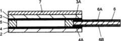
图3是现有的触摸面板的剖面图。在图3中,上基板1是透光性的基板。下基板2同样是透光性的基板。在上基板1的下面形成有透光性的上导电层3,在下基板2的上面形成有下导电层4。FIG. 3 is a sectional view of a conventional touch panel. In FIG. 3 , upper substrate 1 is a light-transmitting substrate. The lower substrate 2 is also a light-transmitting substrate. A translucent upper conductive layer 3 is formed on the lower surface of the upper substrate 1 , and a lower conductive layer 4 is formed on the upper surface of the lower substrate 2 .
并且,在下导电层4的上面以一定的间隔形成点隔板(ドツトスペ—サ)(未图示)。在上导电层3的两端形成有一对上电极3A。在下导电层4的两端形成有下电极4A。Further, dot spacers (dot spacers) (not shown) are formed at regular intervals on the upper surface of the lower conductive layer 4 . A pair of
另外,通过在隔板5上下面涂布形成的粘接层(未图示),将上基板1与下基板2的外周粘合起来,使上导电层3和下导电层4隔开一定的间隙而相对。In addition, by applying an adhesive layer (not shown) formed on the upper and lower surfaces of the
另外,布线基板6为薄膜状,在其上下面形成铜、银等的布线图案6A和布线图案6B。粘附有薄膜状的盖板(未图示),以将除了布线图案6A和布线图案6B的左右端以外的整个面覆盖。In addition, the
该布线基板6的左端被夹持在上基板1和下基板2的右端之间。而且,通过在合成树脂内分散有导电粒子的各向异性导电粘接剂(未图示),将在下基板2的上面延伸出的下电极4A与布线图案6B连接并且电连接,将在上基板1的下面延伸出的上电极3A与布线图案6A连接并且电连接。The left end of the
另外,偏振光板7通过三乙酰纤维素膜夹持偏振光体。该偏振光板7通过在其下面涂布形成的粘接层(未图示)而粘附在上基板1的上面,构成触摸面板。In addition, the polarizing
将如此构成的触摸面板配置在液晶显示元件等的前面而安装在电子设备中。这样,将布线基板6向下弯曲,使布线图案6A和6B的右端通过连接用连接器或锡焊等与设备的电路(未图示)连接。The touch panel configured in this way is arranged on the front surface of a liquid crystal display element or the like to be mounted on an electronic device. In this way, the
在以上的构成中,若一边辨认触摸面板背面的液晶显示元件的显示,一边用手指或笔等按压操作偏振光板7的上面,则上基板1与偏振光板7一起弯曲,被按压处的上导电层3与下导电层4接触。In the above structure, if the display of the liquid crystal display element on the back of the touch panel is recognized, and the upper surface of the polarizing
于是,经由布线基板6的多个布线图案6A或布线图案6B,从电路依次向上导电层3和下导电层4的两端施加电压。通过这些电压,电路检测被按压的位置,进行设备各种功能间的切换。Then, a voltage is sequentially applied to both ends of the upper conductive layer 3 and the lower conductive layer 4 from the circuit via the plurality of
此时,来自于上方的太阳光或灯光等外部光透过偏振光板7时,X方向以及与其垂直的Y方向的光波通过偏振光板7的作用而仅成为其中一个方向的直线偏振光,从偏振光板7向上基板1射入。At this time, when external light such as sunlight or light from above passes through the polarizing
这样,该光透过上基板1被下导电层4向上方反射。但是,由于该反射光如上所述被偏振光板7大致减半,故从偏振光板7射出的反射光减少,使背面的液晶显示元件等容易看到。In this way, the light passes through the upper substrate 1 and is reflected upward by the lower conductive layer 4 . However, since the reflected light is approximately halved by the polarizing
另外,作为与本发明相关的现有技术文献信息,例如(日本)特开2006-11598号公报所公开的内容。In addition, as prior art document information related to the present invention, for example, the content disclosed in (Japanese) Unexamined Patent Application Publication No. 2006-11598.
但是,上述现有的触摸面板中被拉伸的、层积有多种材料且易因热而收缩的偏振光板7粘附在不同材质但外形尺寸基本相同的上基板1的上面。因此,在周围的温度或湿度较高的环境中使用时,由于偏振光板7的收缩,上基板1翘曲,外周从隔板5剥离,使操作变得不稳定,或者,由于上基板的翘曲而使得布线基板6的布线图案6A与上电极3A的电连接变得不稳定。However, in the above-mentioned conventional touch panel, the
发明内容Contents of the invention
本发明的触摸面板是将偏振光板粘附在大致边框状的隔板外周的内侧、上基板的上面而构成的,通过将偏振光板粘附在隔板外周的内侧,即使在高温高湿度下使用,由于粘贴有偏振光板的上基板的翘曲变小,故可以防止从隔板的剥离或布线基板的浮动等,可以得到操作或电连接可靠的触摸面板。The touch panel of the present invention is constituted by adhering a polarizing plate on the inner side of the outer periphery of the roughly frame-shaped partition and on the upper surface of the upper substrate. , Since the warpage of the upper substrate on which the polarizing plate is pasted is reduced, peeling from the spacer or floating of the wiring substrate can be prevented, and a touch panel with reliable operation or electrical connection can be obtained.
本发明的触摸面板包括:上基板,其具有透光性,为可挠性薄膜状,且在下面形成有上导电层;在上面形成有隔开规定空隙与上导电层相对的下导线层的、具有透光性的下基板;位于上基板与下基板之间的大致边框状的隔板;粘附于上基板的上面的偏振光板,偏振光板向所述隔板外周的内侧进行粘附。The touch panel of the present invention includes: an upper substrate, which is light-transmitting and is in the shape of a flexible film, and an upper conductive layer is formed on the lower side; 1. A lower substrate with translucency; a substantially frame-shaped spacer located between the upper substrate and the lower substrate; a polarizing plate adhered to the upper surface of the upper substrate, and the polarizing plate is adhered to the inner side of the outer periphery of the spacer.
附图说明Description of drawings
图1是本发明一实施方式的触摸面板的剖面图。FIG. 1 is a cross-sectional view of a touch panel according to an embodiment of the present invention.
图2是本发明其它实施方式的触摸面板的剖面图。2 is a cross-sectional view of a touch panel according to another embodiment of the present invention.
图3是现有的触摸面板的剖面图。FIG. 3 is a sectional view of a conventional touch panel.
具体实施方式Detailed ways
为了解决以往存在的问题,本发明提供了一种触摸面板,即使在高温高湿度下使用,操作或电连接也稳定。In order to solve the conventional problems, the present invention provides a touch panel whose operation or electrical connection is stable even when it is used under high temperature and high humidity.
以下,使用图1和图2说明本发明的实施方式。Hereinafter, an embodiment of the present invention will be described using FIG. 1 and FIG. 2 .
另外,为了更容易地理解其构成,附图中将厚度方向的尺寸扩大表示。In addition, in order to understand the structure more easily, the dimension of the thickness direction is enlarged and shown in drawing.
此外,与背景技术中说明的构成相同的构成部分标注相同的附图标记。In addition, the same components as those described in the background art are denoted by the same reference numerals.
(实施方式)(implementation mode)
图1是本发明一实施方式的触摸面板的剖面图。在图1中,上基板1是聚碳酸酯或聚醚砜、聚环烯烃等薄膜状的、光学上各向同性的透光性基板。下基板2是玻璃或聚碳酸酯、聚醚砜等光学上各向同性的透光性基板。在上基板1的下面通过溅射法等形成有氧化铟锡或氧化锡等具有透光性的上导电层3,同样,通过溅射法等在下基板2的上面形成有下导电层4。FIG. 1 is a cross-sectional view of a touch panel according to an embodiment of the present invention. In FIG. 1 , an upper substrate 1 is an optically isotropic light-transmitting substrate in the form of a film such as polycarbonate, polyethersulfone, or polycycloolefin. The lower substrate 2 is an optically isotropic light-transmitting substrate such as glass, polycarbonate, polyethersulfone, or the like. A light-transmitting upper conductive layer 3 such as indium tin oxide or tin oxide is formed on the lower surface of the upper substrate 1 by sputtering, and a lower conductive layer 4 is formed on the upper surface of the lower substrate 2 by sputtering.
在下导电层4的上面通过环氧或硅等绝缘树脂以一定间隔形成多个点隔板(未图示)。这样,在上导电层3的两端形成有一对银或石墨等的上电极3A,在下导电层4的两端形成有一对与上电极3A垂直的下电极4A。On the upper surface of the lower conductive layer 4, a plurality of dot spacers (not shown) are formed at regular intervals with an insulating resin such as epoxy or silicon. Thus, a pair of
另外,隔板5为边框状,由聚酯或环氧等形成。通过在该隔板5的上下面或单面上形成的丙烯或橡胶等的粘接层(未图示),将上基板1和下基板2的外周粘合起来,使上导电层3和下导电层4隔开规定的间隙而相对。In addition, the
布线基板6是聚对苯二甲酸乙二醇酯或聚酰亚胺等的薄膜状。在其上下面上形成多个铜或银、石墨等的布线图案6A和布线图案6B,并且,粘附有薄膜状的盖板(未图示),以将布线图案6A和布线图案6B的左右端以外的整个面覆盖。The
该配线基板6的左端被夹持在上基板1的右端和下基板2的右端之间。通过合成树脂内分散有导电粒子的各向异性的导电粘接剂(未图示)而将在下基板2的上面延伸出的下电极4A的端部与布线图案6B的左端连接并且电连接。另外,通过合成树脂内分散有导电粒子的各向异性的导电粘接剂(未图示)而将在上基板1的下面延伸出的上电极3A的端部与布线图案6A的左端连接并且电连接。The left end of the
偏振光板9通过三乙酰纤维素膜夹持偏振光体,该偏振光体将碘元素或染料吸附在聚乙烯醇中并延伸定向。偏振光板9前后左右方向的尺寸比上基板1的外形尺寸小。该偏振光板9通过在下面涂布形成的粘接层(未图示)而粘附在大致边框状的隔板5外周的内侧且上基板1的上面,构成触摸面板10。The
将如此构成的触摸面板10配置在液晶显示元件等的前面而安装在电子设备中,并且,将布线基板6向下弯曲,使布线图案6A和布线图案6B的右端通过连接用连接器或锡焊等与设备的电路(未图示)连接。The
在以上的构成中,若一边辨认触摸面板10背面的液晶显示元件的显示,一边用手指或笔等按压操作偏振光板9的上面,则上基板1与偏振光板9一起弯曲,被按压处的上导电层3与下导电层4接触。In the above configuration, if the upper surface of the
于是,经由布线基板6的多个布线图案6A或布线图案6B,从电路依次向上导电层3和下导电层4的两端施加电源。通过这些电压,电路检测出被按压的位置,进行设备各种功能间的切换。Then, power is sequentially applied to both ends of the upper conductive layer 3 and the lower conductive layer 4 from the circuit via the plurality of
此时,来自上方的太阳光或灯光等外部光透过偏振光板9时,X方向以及与其垂直的Y方向的光波通过偏振光板9的作用成为其中一种方向的直线偏振光,从偏振光板9向上基板1射入。At this time, when external light such as sunlight or light from above passes through the
该光透过上基板1之后,主要在上导电层3或下导电层4、下基板2的下面向上方反射。但是,由于该反射光如上所述地被偏振光板9大致减半,故从偏振光板9上面射出的反射减少,容易看到背面的液晶显示元件等。After passing through the upper substrate 1 , the light is mainly reflected upward from the lower surface of the upper conductive layer 3 or the lower conductive layer 4 and the lower substrate 2 . However, since the reflected light is roughly halved by the
另外,偏振光板9在延伸的同时层积有多种材料,并且容易由于热而收缩,该偏振光板9粘附在材质不同的上基板1的上面。但是,偏振光板9的前后左右方向的尺寸比上基板1的外形尺寸小,并且粘附在大致边框状的隔板5的外周的内侧、上基板1的上面。因此,在周围的温度或湿度高的环境下使用时,也能够使粘附有偏振光板9的上基板1的翘曲较小。In addition, the
即,在高温高湿度下使用时,偏振光板9收缩。由此,上基板1也翘曲,但由于偏振光板9粘附在上基板1上且隔板5外周的内侧,故收缩产生的力不施加在整个上基板1上而施加在局部,上基板1的翘曲变小。因此,上基板1的外周不从隔板5剥离,在布线基板6的布线图案6A与上电极3A之间不产生浮起。That is, when used under high temperature and high humidity, the
这样,根据本实施方式,通过将偏振光板9粘附在大致边框状的隔板5外周的内侧且上基板1的上面,即使在高温高湿度下使用,也能够使粘附有偏振光板9的上基板1的翘曲变小。因此,可防止从隔板5剥离或布线基板6的浮起等,能够得到操作或电连接可靠的触摸面板。Thus, according to the present embodiment, by adhering the
图2是本发明其他的触摸面板的剖面图。图2与图1的不同点在于偏振光板9A。因此,偏振光板9A以外的说明省略,以偏振光板9A为中心进行说明。Fig. 2 is a cross-sectional view of another touch panel of the present invention. The difference between FIG. 2 and FIG. 1 lies in the
如图2所示,该触摸面板11的偏振光板9A的外形尺寸比图1的情况还小,将该偏振光板9粘附在隔板5内周的内侧且上基板1的上面。这样,能够进一步减小上基板1的翘曲。As shown in FIG. 2 , the outer dimensions of the
另外,在以上的说明中,对于将偏振光板9或偏振光板9A粘附在上基板1的上面的结构进行了说明。但本发明也可以将上基板1或下基板2形成为如下的相位差板:即,使聚碳酸酯或环烯烃类等薄膜延伸并具有多种折射性,对1/4波长具有可挠性。另外,本发明也可以在偏振光板9与上基板1之间夹持有相位差板。另外,本发明也可以在下基板2的下面粘附有相位差板等。In addition, in the above description, the structure in which the
由以上的说明可知,本发明的触摸面板具有可使操作或电连接可靠的有益效果,并且主要用作为各种电子设备的操作用。As can be seen from the above description, the touch panel of the present invention has the beneficial effect of enabling reliable operation or electrical connection, and is mainly used for the operation of various electronic devices.
Claims (1)
Applications Claiming Priority (2)
| Application Number | Priority Date | Filing Date | Title |
|---|---|---|---|
| JP2006051713AJP2007233513A (en) | 2006-02-28 | 2006-02-28 | Touch panel |
| JP051713/06 | 2006-02-28 |
Publications (2)
| Publication Number | Publication Date |
|---|---|
| CN101030115A CN101030115A (en) | 2007-09-05 |
| CN100465870Ctrue CN100465870C (en) | 2009-03-04 |
Family
ID=38443205
Family Applications (1)
| Application Number | Title | Priority Date | Filing Date |
|---|---|---|---|
| CNB2007100843267AActiveCN100465870C (en) | 2006-02-28 | 2007-02-27 | touch panel |
Country Status (3)
| Country | Link |
|---|---|
| US (1) | US20070200259A1 (en) |
| JP (1) | JP2007233513A (en) |
| CN (1) | CN100465870C (en) |
Families Citing this family (8)
| Publication number | Priority date | Publication date | Assignee | Title |
|---|---|---|---|---|
| JP2008204320A (en)* | 2007-02-22 | 2008-09-04 | Matsushita Electric Ind Co Ltd | Touch panel |
| JP5098798B2 (en)* | 2008-05-16 | 2012-12-12 | パナソニック株式会社 | Touch panel and input device using the same |
| CN102089735A (en)* | 2008-08-07 | 2011-06-08 | 夏普株式会社 | Touch panel, display, and electronic device |
| TWI426426B (en) | 2009-12-31 | 2014-02-11 | Au Optronics Corp | Touch-sensing display module and touch-sensing module thereof |
| CN101763204B (en)* | 2010-01-18 | 2012-10-31 | 友达光电股份有限公司 | Touch display device and touch module included therein |
| KR101640615B1 (en)* | 2011-10-27 | 2016-07-19 | 주식회사 엘지화학 | Method for preparing transparent conductive film |
| US9116390B2 (en) | 2012-08-27 | 2015-08-25 | Microsoft Technology Licensing, Llc | Touch sensing liquid crystal display compatible with linearly polarized sunglasses |
| KR102158802B1 (en) | 2013-10-31 | 2020-09-23 | 삼성디스플레이 주식회사 | Display panel and liquid crystal display |
Citations (2)
| Publication number | Priority date | Publication date | Assignee | Title |
|---|---|---|---|---|
| CN1416002A (en)* | 2001-11-02 | 2003-05-07 | 奇美电子股份有限公司 | Touch LCD panel device |
| JP2004109816A (en)* | 2002-09-20 | 2004-04-08 | Seiko Epson Corp | Electro-optical device, method of manufacturing electro-optical device, and electronic apparatus |
Family Cites Families (3)
| Publication number | Priority date | Publication date | Assignee | Title |
|---|---|---|---|---|
| JP3231820B2 (en)* | 1991-12-17 | 2001-11-26 | ソニー株式会社 | Liquid crystal display |
| JP2000207128A (en)* | 1999-01-18 | 2000-07-28 | Matsushita Electric Ind Co Ltd | Transparent touch panel and electronic device using the same |
| JP4052287B2 (en)* | 2004-06-22 | 2008-02-27 | セイコーエプソン株式会社 | Electro-optical device, electronic apparatus, and method of manufacturing electro-optical device |
- 2006
- 2006-02-28JPJP2006051713Apatent/JP2007233513A/enactivePending
- 2007
- 2007-02-12USUS11/704,960patent/US20070200259A1/ennot_activeAbandoned
- 2007-02-27CNCNB2007100843267Apatent/CN100465870C/enactiveActive
Patent Citations (2)
| Publication number | Priority date | Publication date | Assignee | Title |
|---|---|---|---|---|
| CN1416002A (en)* | 2001-11-02 | 2003-05-07 | 奇美电子股份有限公司 | Touch LCD panel device |
| JP2004109816A (en)* | 2002-09-20 | 2004-04-08 | Seiko Epson Corp | Electro-optical device, method of manufacturing electro-optical device, and electronic apparatus |
Also Published As
| Publication number | Publication date |
|---|---|
| JP2007233513A (en) | 2007-09-13 |
| US20070200259A1 (en) | 2007-08-30 |
| CN101030115A (en) | 2007-09-05 |
Similar Documents
| Publication | Publication Date | Title |
|---|---|---|
| CN100465870C (en) | touch panel | |
| US8264469B2 (en) | Touch panel and display unit | |
| JP5084698B2 (en) | Touch panel and touch panel display device | |
| US20110043465A1 (en) | Touch panel having a insulation layer | |
| US8576190B2 (en) | Touch panel and display device including the same | |
| CN101251663A (en) | Touch panel | |
| CN101446881B (en) | touch screen | |
| CN100511116C (en) | Method for manufacturing touch panel | |
| TWI595220B (en) | Pressure sensing device and manufacturing method thereof | |
| CN101581996A (en) | Touch panel and input device using same | |
| CN101286106A (en) | touch panel | |
| JP4367295B2 (en) | Touch panel | |
| CN204242150U (en) | a display device | |
| CN1326024C (en) | Touch panel | |
| KR102173612B1 (en) | Sensor unit and input device with the sensor unit | |
| CN101251664A (en) | input device | |
| KR20160076298A (en) | Touch input device | |
| CN1936812A (en) | Touch panel | |
| CN100456222C (en) | touch panel | |
| CN1804775A (en) | Touch panel | |
| JP2010108222A (en) | Touch panel and touch panel type display device | |
| CN110489003A (en) | Show equipment | |
| JP2004227192A (en) | Touch panel and entry-via-screen type display unit including it | |
| TWI395999B (en) | Touch panel | |
| JP2014081870A (en) | Touch panel |
Legal Events
| Date | Code | Title | Description |
|---|---|---|---|
| C06 | Publication | ||
| PB01 | Publication | ||
| C10 | Entry into substantive examination | ||
| SE01 | Entry into force of request for substantive examination | ||
| C14 | Grant of patent or utility model | ||
| GR01 | Patent grant |