CN100461340C - Method for producing group III nitride-based compound semiconductor - Google Patents
Method for producing group III nitride-based compound semiconductorDownload PDFInfo
- Publication number
- CN100461340C CN100461340CCNB2004101021001ACN200410102100ACN100461340CCN 100461340 CCN100461340 CCN 100461340CCN B2004101021001 ACNB2004101021001 ACN B2004101021001ACN 200410102100 ACN200410102100 ACN 200410102100ACN 100461340 CCN100461340 CCN 100461340C
- Authority
- CN
- China
- Prior art keywords
- compound semiconductor
- group iii
- iii nitride
- substrate
- buffer layer
- Prior art date
- Legal status (The legal status is an assumption and is not a legal conclusion. Google has not performed a legal analysis and makes no representation as to the accuracy of the status listed.)
- Expired - Lifetime
Links
Images


Classifications
- H—ELECTRICITY
- H10—SEMICONDUCTOR DEVICES; ELECTRIC SOLID-STATE DEVICES NOT OTHERWISE PROVIDED FOR
- H10H—INORGANIC LIGHT-EMITTING SEMICONDUCTOR DEVICES HAVING POTENTIAL BARRIERS
- H10H20/00—Individual inorganic light-emitting semiconductor devices having potential barriers, e.g. light-emitting diodes [LED]
- H10H20/01—Manufacture or treatment
- H10H20/011—Manufacture or treatment of bodies, e.g. forming semiconductor layers
- H10H20/013—Manufacture or treatment of bodies, e.g. forming semiconductor layers having light-emitting regions comprising only Group III-V materials
- H10H20/0133—Manufacture or treatment of bodies, e.g. forming semiconductor layers having light-emitting regions comprising only Group III-V materials with a substrate not being Group III-V materials
- H10H20/01335—Manufacture or treatment of bodies, e.g. forming semiconductor layers having light-emitting regions comprising only Group III-V materials with a substrate not being Group III-V materials the light-emitting regions comprising nitride materials
- H—ELECTRICITY
- H01—ELECTRIC ELEMENTS
- H01L—SEMICONDUCTOR DEVICES NOT COVERED BY CLASS H10
- H01L21/00—Processes or apparatus adapted for the manufacture or treatment of semiconductor or solid state devices or of parts thereof
- H01L21/02—Manufacture or treatment of semiconductor devices or of parts thereof
- H01L21/02104—Forming layers
- H01L21/02365—Forming inorganic semiconducting materials on a substrate
- H01L21/02367—Substrates
- H01L21/0237—Materials
- H01L21/0242—Crystalline insulating materials
- H—ELECTRICITY
- H01—ELECTRIC ELEMENTS
- H01L—SEMICONDUCTOR DEVICES NOT COVERED BY CLASS H10
- H01L21/00—Processes or apparatus adapted for the manufacture or treatment of semiconductor or solid state devices or of parts thereof
- H01L21/02—Manufacture or treatment of semiconductor devices or of parts thereof
- H01L21/02104—Forming layers
- H01L21/02365—Forming inorganic semiconducting materials on a substrate
- H01L21/02436—Intermediate layers between substrates and deposited layers
- H01L21/02439—Materials
- H01L21/02455—Group 13/15 materials
- H01L21/02458—Nitrides
- H—ELECTRICITY
- H01—ELECTRIC ELEMENTS
- H01L—SEMICONDUCTOR DEVICES NOT COVERED BY CLASS H10
- H01L21/00—Processes or apparatus adapted for the manufacture or treatment of semiconductor or solid state devices or of parts thereof
- H01L21/02—Manufacture or treatment of semiconductor devices or of parts thereof
- H01L21/02104—Forming layers
- H01L21/02365—Forming inorganic semiconducting materials on a substrate
- H01L21/02518—Deposited layers
- H01L21/02521—Materials
- H01L21/02538—Group 13/15 materials
- H01L21/0254—Nitrides
- H—ELECTRICITY
- H01—ELECTRIC ELEMENTS
- H01L—SEMICONDUCTOR DEVICES NOT COVERED BY CLASS H10
- H01L21/00—Processes or apparatus adapted for the manufacture or treatment of semiconductor or solid state devices or of parts thereof
- H01L21/02—Manufacture or treatment of semiconductor devices or of parts thereof
- H01L21/02104—Forming layers
- H01L21/02365—Forming inorganic semiconducting materials on a substrate
- H01L21/02612—Formation types
- H01L21/02617—Deposition types
- H01L21/0262—Reduction or decomposition of gaseous compounds, e.g. CVD
- H—ELECTRICITY
- H01—ELECTRIC ELEMENTS
- H01L—SEMICONDUCTOR DEVICES NOT COVERED BY CLASS H10
- H01L21/00—Processes or apparatus adapted for the manufacture or treatment of semiconductor or solid state devices or of parts thereof
- H01L21/02—Manufacture or treatment of semiconductor devices or of parts thereof
- H01L21/02104—Forming layers
- H01L21/02365—Forming inorganic semiconducting materials on a substrate
- H01L21/02612—Formation types
- H01L21/02617—Deposition types
- H01L21/02636—Selective deposition, e.g. simultaneous growth of mono- and non-monocrystalline semiconductor materials
- H01L21/02639—Preparation of substrate for selective deposition
- H—ELECTRICITY
- H01—ELECTRIC ELEMENTS
- H01L—SEMICONDUCTOR DEVICES NOT COVERED BY CLASS H10
- H01L21/00—Processes or apparatus adapted for the manufacture or treatment of semiconductor or solid state devices or of parts thereof
- H01L21/02—Manufacture or treatment of semiconductor devices or of parts thereof
- H01L21/02104—Forming layers
- H01L21/02365—Forming inorganic semiconducting materials on a substrate
- H01L21/02612—Formation types
- H01L21/02617—Deposition types
- H01L21/02636—Selective deposition, e.g. simultaneous growth of mono- and non-monocrystalline semiconductor materials
- H01L21/02647—Lateral overgrowth
- H01L21/0265—Pendeoepitaxy
- H—ELECTRICITY
- H01—ELECTRIC ELEMENTS
- H01S—DEVICES USING THE PROCESS OF LIGHT AMPLIFICATION BY STIMULATED EMISSION OF RADIATION [LASER] TO AMPLIFY OR GENERATE LIGHT; DEVICES USING STIMULATED EMISSION OF ELECTROMAGNETIC RADIATION IN WAVE RANGES OTHER THAN OPTICAL
- H01S2304/00—Special growth methods for semiconductor lasers
- H01S2304/12—Pendeo epitaxial lateral overgrowth [ELOG], e.g. for growing GaN based blue laser diodes
- H—ELECTRICITY
- H01—ELECTRIC ELEMENTS
- H01S—DEVICES USING THE PROCESS OF LIGHT AMPLIFICATION BY STIMULATED EMISSION OF RADIATION [LASER] TO AMPLIFY OR GENERATE LIGHT; DEVICES USING STIMULATED EMISSION OF ELECTROMAGNETIC RADIATION IN WAVE RANGES OTHER THAN OPTICAL
- H01S5/00—Semiconductor lasers
- H01S5/02—Structural details or components not essential to laser action
- H01S5/0206—Substrates, e.g. growth, shape, material, removal or bonding
- H01S5/0213—Sapphire, quartz or diamond based substrates
- H—ELECTRICITY
- H01—ELECTRIC ELEMENTS
- H01S—DEVICES USING THE PROCESS OF LIGHT AMPLIFICATION BY STIMULATED EMISSION OF RADIATION [LASER] TO AMPLIFY OR GENERATE LIGHT; DEVICES USING STIMULATED EMISSION OF ELECTROMAGNETIC RADIATION IN WAVE RANGES OTHER THAN OPTICAL
- H01S5/00—Semiconductor lasers
- H01S5/30—Structure or shape of the active region; Materials used for the active region
- H01S5/32—Structure or shape of the active region; Materials used for the active region comprising PN junctions, e.g. hetero- or double- heterostructures
- H01S5/323—Structure or shape of the active region; Materials used for the active region comprising PN junctions, e.g. hetero- or double- heterostructures in AIIIBV compounds, e.g. AlGaAs-laser, InP-based laser
- H01S5/32308—Structure or shape of the active region; Materials used for the active region comprising PN junctions, e.g. hetero- or double- heterostructures in AIIIBV compounds, e.g. AlGaAs-laser, InP-based laser emitting light at a wavelength less than 900 nm
- H01S5/32341—Structure or shape of the active region; Materials used for the active region comprising PN junctions, e.g. hetero- or double- heterostructures in AIIIBV compounds, e.g. AlGaAs-laser, InP-based laser emitting light at a wavelength less than 900 nm blue laser based on GaN or GaP
- H—ELECTRICITY
- H10—SEMICONDUCTOR DEVICES; ELECTRIC SOLID-STATE DEVICES NOT OTHERWISE PROVIDED FOR
- H10H—INORGANIC LIGHT-EMITTING SEMICONDUCTOR DEVICES HAVING POTENTIAL BARRIERS
- H10H20/00—Individual inorganic light-emitting semiconductor devices having potential barriers, e.g. light-emitting diodes [LED]
- H10H20/80—Constructional details
- H10H20/81—Bodies
- H10H20/8215—Bodies characterised by crystalline imperfections, e.g. dislocations; characterised by the distribution of dopants, e.g. delta-doping
Landscapes
- Engineering & Computer Science (AREA)
- Microelectronics & Electronic Packaging (AREA)
- Physics & Mathematics (AREA)
- Condensed Matter Physics & Semiconductors (AREA)
- General Physics & Mathematics (AREA)
- Manufacturing & Machinery (AREA)
- Computer Hardware Design (AREA)
- Power Engineering (AREA)
- Chemical & Material Sciences (AREA)
- Crystallography & Structural Chemistry (AREA)
- Materials Engineering (AREA)
- Led Devices (AREA)
- Semiconductor Lasers (AREA)
- Crystals, And After-Treatments Of Crystals (AREA)
Abstract
Translated fromChinese
Description
Translated fromChinese本申请是申请日为2001年2月23日的第01809479.1号发明专利申请的分案申请。This application is a divisional application of the No. 01809479.1 patent application for invention filed on February 23, 2001.
技术领域technical field
本发明涉及一种制造III族氮化物系化合物半导体的方法。更具体的说,本发明涉及一种采用外延横向附晶生长(epitaxial lateral overgrowth)(ELO)制造III族氮化物系化合物半导体的方法、III族氮化物系化合物半导体器件以及III族氮化物系化合物半导体衬底。III族氮化物系化合物半导体一般由AlxGayIn1-x-yN(其中,0≤x≤1,0≤y≤1,且0≤x+y≤1)表示,其示例包括诸如AlN、GaN的二元半导体;诸如AlxGa1-xN、AlxIn1-xN、以及GaxIn1-xN(其中0<x<1)的三元化合物半导体;以及诸如AlxGayIn1-x-yN(其中,0<x<1,0<y<1,且0<x+y<1)的四元化合物半导体。The present invention relates to a method for producing a Group III nitride compound semiconductor. More specifically, the present invention relates to a method for manufacturing III-nitride compound semiconductors using epitaxial lateral overgrowth (ELO), a III-nitride compound semiconductor device, and a III-nitride compound semiconductor semiconductor substrate. Group III nitride-based compound semiconductors are generally represented byAlxGayIn1-xyN (where 0≤x≤1, 0≤y≤1, and0≤x +y≤1), examples of which include AlN, Binary semiconductors of GaN; ternary compound semiconductors such asAlxGa1-xN ,AlxIn1-xN , andGaxIn1-xN (where 0<x<1); and such asAlxGa A quaternary compound semiconductor ofy In1-xy N (wherein, 0<x<1, 0<y<1, and 0<x+y<1).
在本说明书中,除非另外指定,“III族氮化物系化合物半导体”包括掺杂有杂质以呈现出p型或n型导电性的III族氮化物系化合物半导体。In this specification, unless otherwise specified, a "group III nitride-based compound semiconductor" includes a group III nitride-based compound semiconductor doped with impurities to exhibit p-type or n-type conductivity.
背景技术Background technique
III族氮化物系化合物半导体为当用于诸如发光器件的器件中呈现出从UV到红光的大范围发射光谱的直接迁移型半导体,并且已经在诸如发光二极管(LED)和激光二极管(LD)之类的器件中得以应用。另外,由于他们的较宽的带隙,认为采用上述半导体的器件与采用其他类型半导体的器件相比在高温下呈现出可靠的工作特性,并因此积极地对他们在诸如FET的晶体管中的应用加以研究。此外,由于III族氮化物系化合物半导体不包含砷(As)作为主要元素,从环境方面上已经期望III族氮化物系化合物半导体应用于各种半导体器件中。这些III族氮化物系化合物半导体一般形成在蓝宝石衬底上。Group III nitride-based compound semiconductors are direct-transition semiconductors that exhibit a wide range of emission spectra from UV to red when used in devices such as light-emitting devices, and have been used in devices such as light-emitting diodes (LEDs) and laser diodes (LDs) Applied in such devices. In addition, due to their wide bandgap, devices employing the above-mentioned semiconductors are considered to exhibit reliable operating characteristics at high temperatures compared with devices employing other types of semiconductors, and thus their application to transistors such as FETs has been actively pursued. Be researched. In addition, since group III nitride compound semiconductors do not contain arsenic (As) as a main element, application of group III nitride compound semiconductors to various semiconductor devices has been expected from an environmental point of view. These Group III nitride-based compound semiconductors are generally formed on a sapphire substrate.
发明内容Contents of the invention
然而,当III族氮化物系化合物半导体形成在蓝宝石衬底上时,由于蓝宝石的晶格常数与半导体晶格常数之间的差异而发生失配诱发的位错,导致器件特性较差。失配诱发的位错为在纵向(即,在垂直于衬底表面的方向)穿透半导体层的线位错(threading dislocation),且III族氮化物系化合物半导体伴随有如下问题,即,大约109cm-2大小的位错通过其扩散。上述位错通过由不同成份的III族氮化物系化合物半导体所形成的层扩散,直到他们到达最上层。当这种半导体植入例如一种发光器件中时,该器件呈现出在LD阈值电流、LED或LD寿命等方面的器件特性不令人满意的问题。另一方面,当III族氮化物系半导体植入任何其他类型的半导体器件中时,由于电子因III族氮化物系化合物半导体中的缺陷而扩散,因此,半导体器件成为具有较低的迁移率。这些问题即使在采用其他类型的衬底情况下也未解决。However, when a Group III nitride-based compound semiconductor is formed on a sapphire substrate, mismatch-induced dislocations occur due to the difference between the lattice constant of sapphire and the semiconductor lattice constant, resulting in poor device characteristics. Mismatch-induced dislocations are threading dislocations that penetrate the semiconductor layer in the longitudinal direction (that is, in a direction perpendicular to the substrate surface), and group III nitride-based compound semiconductors are accompanied by the problem that approximately Dislocations of size 109 cm-2 diffuse through it. The above-mentioned dislocations diffuse through layers formed of Group III nitride-based compound semiconductors of different compositions until they reach the uppermost layer. When such a semiconductor is implanted in, for example, a light-emitting device, the device exhibits unsatisfactory device characteristics in terms of LD threshold current, LED or LD lifetime, and the like. On the other hand, when a Group III nitride-based semiconductor is implanted in any other type of semiconductor device, since electrons diffuse due to defects in the Group III nitride-based compound semiconductor, the semiconductor device becomes to have lower mobility. These problems are not resolved even with other types of substrates.
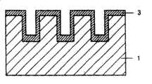
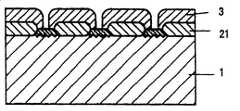
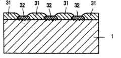
下面,将参照图18的示意图描述上述位错。图18示出了衬底91、其上形成的缓冲层92、以及进一步形成于其上的III族氮化物系化合物半导体层93。传统上,衬底91由蓝宝石或类似的物质形成,而缓冲层92由氮化铝(AlN)或类似物质形成。设置氮化铝(AlN)形成的缓冲层92以缓和蓝宝石衬底91和III族氮化物系化合物半导体层93之间的失配。然而,位错的产生不能减小到零。线位错901从位错初始点900向上(在相对于衬底表面的垂直方向上)移动,穿透缓冲层92和III族氮化物系化合物半导体层93。当半导体器件是通过将所关注的各种类型的III族氮化物系化合物半导体层叠置在III族氮化物系化合物半导体层93上而制造时,线位错从III族氮化物系化合物半导体层93表面上的位错抵达点902经过半导体器件进一步向上扩散。由此,根据传统技术,在形成III族氮化物系化合物半导体层过程中不能防止位错的成问题的移动。Next, the above-mentioned dislocation will be described with reference to the schematic diagram of FIG. 18 . FIG. 18 shows a
本发明已经本着试图解决上述问题而完成,本发明的目的是在抑制线位错产生的情况下制造III族氮化物系化合物半导体。The present invention has been made in an attempt to solve the above-mentioned problems, and an object of the present invention is to manufacture a group III nitride-based compound semiconductor while suppressing the generation of linear dislocations.
为了实现上述目的,呈现第一特征的本发明提供了一种在衬底上制造III族氮化物系化合物半导体的方法,该方法包括去除衬底表面的至少一部分,以在衬底表面上提供一个沟槽/立柱(trench/post)或沟槽/台地(trench/mesa),以及以衬底未被去除的表面的顶面作用为籽晶,在所述衬底的未被去除表面上垂直且横向地外延生长所需的III族氮化物系化合物半导体,从而覆盖所述衬底沟槽之上的上部,衬底未去除的表面通过去除衬底的一部分而形成,从而形成岛状结构,如点状、带形或网格状结构。In order to achieve the above objects, the present invention exhibiting a first feature provides a method of manufacturing a group III nitride-based compound semiconductor on a substrate, the method including removing at least a part of the surface of the substrate to provide a trench/post or trench/mesa, and seeded with the top surface of the unremoved surface of the substrate, vertical and The desired III-nitride-based compound semiconductor is epitaxially grown laterally so as to cover the upper portion above the substrate trench, and the unremoved surface of the substrate is formed by removing a part of the substrate to form an island-like structure such as Dot, strip or grid structure.
呈现第二特征的本发明提供了一种制造III族氮化物系化合物半导体的方法,其中,III族氮化物系化合物半导体在衬底上形成的缓冲层上生长,该方法包括去除衬底表面的至少一部分,从而在衬底表面上提供一个沟槽/立柱,以及以形成在衬底剩余表面上的缓冲层作用为用于晶体生长的籽晶或晶核,垂直且横向地外延生长所需的III族氮化物系化合物半导体,从而覆盖衬底的沟槽/立柱中的沟槽的上部,缓冲层形成为岛状结构,如点状、带形、或网格状结构。The present invention exhibiting the second feature provides a method of producing a group III nitride-based compound semiconductor, wherein the group III nitride-based compound semiconductor is grown on a buffer layer formed on a substrate, the method comprising removing At least a part, thereby providing a groove/pillar on the substrate surface, and with the buffer layer formed on the remaining surface of the substrate acting as a seed crystal or crystal nucleus for crystal growth, required for epitaxial growth vertically and laterally Group III nitride-based compound semiconductors to cover the upper part of the trenches/pillars of the substrate, and the buffer layer is formed into an island-like structure, such as a dot-like, strip-like, or grid-like structure.
呈现第三特征的本发明提供了一种制造III族氮化物系化合物半导体的方法,其中,III族氮化物系化合物半导体生长于衬底上形成的缓冲层之上,该方法包括去除衬底表面的至少一部分,以在衬底表面上提供一个沟槽/立柱,在衬底上形成缓冲层,在缓冲层上垂直地外延生长III族氮化物系化合物半导体,从而形成单晶层,以及以形成在衬底剩余表面上的缓冲层上的III族氮化物系化合物半导体的单晶层作用为晶体生长的籽晶,垂直且横向外延生长所需的III族氮化物系化合物半导体,从而覆盖衬底的沟槽/立柱中的沟槽的上部,该单晶层形成为岛状结构,诸如点状、带形、或网格状结构。The present invention exhibiting a third feature provides a method of producing a group III nitride-based compound semiconductor, wherein the group III nitride-based compound semiconductor is grown over a buffer layer formed on a substrate, the method comprising removing a surface of the substrate at least a part of the substrate surface to provide a groove/pillar on the substrate surface, form a buffer layer on the substrate, vertically epitaxially grow a Group III nitride compound semiconductor on the buffer layer to form a single crystal layer, and to form The single crystal layer of the group III nitride compound semiconductor on the buffer layer on the remaining surface of the substrate acts as a seed crystal for crystal growth, and the desired group III nitride compound semiconductor is epitaxially grown vertically and laterally, thereby covering the substrate On top of the trenches/pillars, the single crystal layer is formed into an island-like structure, such as a dot-like, ribbon-like, or grid-like structure.
呈现第四特征的本发明提供了一种制造III族氮化物系化合物半导体的方法,其中,III族氮化物系化合物半导体生长于衬底上形成的缓冲层之上,该方法包括在衬底上形成缓冲层;去除缓冲层和衬底表面的至少一部分,从而提供沟槽/立柱,该沟槽/立柱具有其上在衬底表面上形成缓冲层的立柱或台地、以及其上不形成缓冲层的沟槽;以及以形成在衬底剩余表面上的缓冲层作用为用于晶体生长的籽晶,垂直并横向外延生长所需的III族氮化物系化合物半导体,从而覆盖衬底的沟槽/立柱中的沟槽的上部,缓冲层形成为岛状结构,如点状、带形、或网格状结构。The present invention exhibiting a fourth feature provides a method of producing a group III nitride-based compound semiconductor, wherein the group III nitride-based compound semiconductor is grown over a buffer layer formed on a substrate, the method comprising forming a buffer layer; removing the buffer layer and at least a portion of the substrate surface, thereby providing a trench/post having a post or mesa on which the buffer layer is formed on the substrate surface, and no buffer layer formed thereon and using the buffer layer formed on the remaining surface of the substrate as a seed crystal for crystal growth, vertically and laterally epitaxially grow the desired group III nitride-based compound semiconductor, thereby covering the groove/s of the substrate On the upper part of the groove in the column, the buffer layer is formed into an island-like structure, such as a dot-like, strip-like, or grid-like structure.
呈现第五特征的本发明提供了一种制造III族氮化物系化合物半导体的方法,其中,III族氮化物系化合物半导体生长于衬底上形成的缓冲层上,该方法包括在衬底上形成缓冲层;在缓冲层上垂直外延生长III族氮化物系化合物半导体,从而形成单晶层;去除III族氮化物系化合物半导体的单晶层、缓冲层和衬底表面的至少一部分,从而提供一沟槽/立柱,该沟槽/立柱具有其上在衬底表面上形成III族氮化物系化合物半导体的单晶层和缓冲层的立柱、以及其上不形成III族氮化物系化合物半导体的单晶层和缓冲层的沟槽;以及以形成在衬底剩余表面上的缓冲层上的III族氮化物系化合物半导体的单晶层作用为用于晶体生长的籽晶,垂直且横向外延生长所需的III族氮化物系化合物半导体,从而覆盖衬底的沟槽/立柱中的沟槽的上部,单晶层形成为岛状结构,如点状、带形、或网格状结构。The present invention exhibiting a fifth feature provides a method of producing a group III nitride-based compound semiconductor, wherein the group III nitride-based compound semiconductor is grown on a buffer layer formed on a substrate, the method comprising forming buffer layer; vertical epitaxial growth of group III nitride compound semiconductor on the buffer layer, thereby forming a single crystal layer; removing at least a part of the single crystal layer, buffer layer and substrate surface of group III nitride compound semiconductor, thereby providing a A trench/column having a column on which a single crystal layer of a Group III nitride compound semiconductor and a buffer layer are formed on a substrate surface, and a single crystal layer on which a Group III nitride compound semiconductor is not formed. the grooves of the crystal layer and the buffer layer; and with the single crystal layer of the group III nitride compound semiconductor formed on the buffer layer on the remaining surface of the substrate as a seed crystal for crystal growth, vertical and lateral epitaxial growth The desired Group III nitride-based compound semiconductor is used to cover the upper portion of the trenches/pillars of the substrate, and the single crystal layer is formed into an island-like structure, such as a dot-like, strip-like, or grid-like structure.
呈现第六特征的本发明提供了一种制造III族氮化物系化合物半导体的方法,其中,III族氮化物系化合物半导体生长于衬底上,该方法包括降低衬底表面至少一部分的光洁度并在衬底表面上形成其上将不充分形成III族氮化物系化合物半导体层的一部分的表面处理过程,在所述经处理的衬底上生长III族氮化物系化合物半导体并形成其上充分形成III族氮化物系化合物半导体的单晶层的一部分和其上不充分形成III族氮化物系化合物半导体单晶层的一部分的过程,以及以形成在衬底的其表面光洁度未降低的部分上的III族氮化物系化合物半导体的单晶层作用为晶体生长的籽晶,垂直并横向外延生长III族氮化物系化合物半导体,从而覆盖其上III族氮化物系化合物半导体单晶层未充分形成的部分的过程,该单晶层形成为岛状结构,如点状、带形、或网格状结构。The present invention exhibiting a sixth feature provides a method of manufacturing a group III nitride-based compound semiconductor, wherein the group III nitride-based compound semiconductor is grown on a substrate, the method comprising reducing the smoothness of at least a part of the surface of the substrate and A surface treatment process for forming a portion of a group III nitride-based compound semiconductor layer on which a group III nitride-based compound semiconductor layer will not be sufficiently formed on the surface of a substrate, on which a group III nitride-based compound semiconductor layer is grown and formed thereon is sufficiently formed Part of single crystal layer of group nitride compound semiconductor and part of single crystal layer of group III nitride compound semiconductor insufficiently formed thereon, and process of forming III on part of substrate whose surface roughness is not lowered The single-crystal layer of the group-nitride-based compound semiconductor serves as a seed crystal for crystal growth, and the group-III nitride-based compound semiconductor is epitaxially grown vertically and laterally, thereby covering the part where the group-III nitride-based compound semiconductor single-crystal layer is not sufficiently formed process, the single crystal layer is formed into an island-like structure, such as a dot-like, ribbon-like, or grid-like structure.
呈现第七特征的本发明提供了一种制造III族氮化物系化合物半导体的方法,其中III族氮化物系化合物半导体生长于衬底上形成的缓冲层上,该方法包括降低衬底表面的至少一部分的光洁度并于衬底表面上形成其上将充分形成缓冲层的一部分的表面处理过程,在经处理的衬底上生长缓冲层并形成其上充分形成缓冲层的一部分和其上未充分形成缓冲层的一部分的过程,以及以形成在衬底的其表面光洁度未降低的部分上的缓冲层作用为晶体生长的籽晶,垂直并横向外延生长所需的III族氮化物系化合物半导体,从而覆盖其上缓冲层未充分形成的部分的过程,缓冲层形成为岛状结构,如点状、带形或网格状结构。The present invention exhibiting a seventh feature provides a method of producing a group III nitride-based compound semiconductor in which the group III nitride-based compound semiconductor is grown on a buffer layer formed on a substrate, the method comprising lowering at least A surface treatment process for smoothing and forming a portion of a substrate surface on which a buffer layer will be sufficiently formed, growing a buffer layer on a treated substrate and forming a portion on which a buffer layer is substantially formed and on which a buffer layer is not sufficiently formed A process of a part of the buffer layer, and with the buffer layer formed on the portion of the substrate whose surface roughness is not lowered as a seed crystal for crystal growth, vertically and laterally epitaxially grow the desired Group III nitride-based compound semiconductor, thereby The process of covering a portion on which a buffer layer is not sufficiently formed, and the buffer layer is formed into an island-like structure, such as a dot, band, or grid-like structure.
呈现第八特征的本发明提供了一种制造III族氮化物系化合物半导体的方法,其中III族氮化物系化合物半导体生长于衬底上形成的缓冲层上,该方法包括降低衬底表面的至少一部分的光洁度并在衬底表面上形成其上将充分形成缓冲层的一部分的表面处理过程,在经处理的衬底上生长缓冲层并形成其上充分形成缓冲层的一部分和其上未充分形成缓冲层的一部分的过程,在其上充分形成缓冲层的部分上形成III族氮化物系化合物半导体的单晶层的过程,以及以形成在衬底的其表面光洁度未降低的部分上形成的缓冲层上的III族氮化物系化合物半导体的单晶层作用为晶体生长的籽晶,垂直并横向外延生长所需的III族氮化物系化合物半导体,从而覆盖其上未充分形成缓冲层的部分的过程,III族氮化物系化合物半导体的单晶层形成为岛状结构,如点状、带形、或网格状结构。The present invention exhibiting an eighth feature provides a method of producing a group III nitride-based compound semiconductor in which the group III nitride-based compound semiconductor is grown on a buffer layer formed on a substrate, the method comprising lowering at least A surface treatment process for smoothing and forming a portion of a substrate surface on which a buffer layer will be sufficiently formed, growing a buffer layer on a treated substrate and forming a portion on which a buffer layer is sufficiently formed and on which a buffer layer is not sufficiently formed A process of forming a part of a buffer layer, a process of forming a single crystal layer of a group III nitride compound semiconductor on a portion on which a buffer layer is sufficiently formed, and a process of forming a buffer formed on a portion of a substrate whose surface roughness is not degraded The single crystal layer of the Group III nitride compound semiconductor on the layer acts as a seed crystal for crystal growth, and the required Group III nitride compound semiconductor is epitaxially grown vertically and laterally, thereby covering the part where the buffer layer is not sufficiently formed. During the process, the single crystal layer of the Group III nitride compound semiconductor is formed into an island-like structure, such as a dot-like, band-like, or grid-like structure.
呈现第九特征的本发明提供了一种制造III族氮化物系化合物半导体的方法,其中III族氮化物系化合物半导体生长于衬底上形成的缓冲层上,该方法包括在衬底上形成缓冲层的过程,降低缓冲层表面至少一部分的光洁度并形成其上将不充分形成III族氮化物系化合物半导体的单晶层的一部分的表面处理过程,以缓冲层的其表面光洁度未降低的部分作用为晶体生长的籽晶,垂直并横向外延生长所需III族氮化物系化合物半导体,从而覆盖缓冲层的光洁度降低的部分的过程,缓冲层的该部分形成为岛状结构,如点状、带形、或网格状结构。The present invention exhibiting a ninth feature provides a method of producing a group III nitride-based compound semiconductor in which the group III nitride-based compound semiconductor is grown on a buffer layer formed on a substrate, the method comprising forming the buffer layer on the substrate layer process, a surface treatment process that reduces the smoothness of at least a part of the surface of the buffer layer and forms a part of a single crystal layer on which a group III nitride-based compound semiconductor will not be sufficiently formed, acting on the part of the buffer layer whose surface roughness is not reduced The process of vertically and laterally epitaxially growing the desired group III nitride compound semiconductor as the seed crystal for crystal growth, thereby covering the part of the buffer layer whose smoothness is reduced, and the part of the buffer layer is formed into an island-like structure, such as dots, bands, etc. shape, or grid-like structure.
在呈现第十特征的本发明中提供了一种制造III族氮化物系化合物半导体的方法,其中III族氮化物系化合物半导体生长于衬底上形成的缓冲层上,该方法包括在衬底上形成缓冲层的过程,在缓冲层上形成第一III族氮化物系化合物半导体的过程,降低第一III族氮化物系化合物半导体至少一部分的光洁度并形成其上将不充分形成第二III族氮化物系化合物半导体的单晶层的一部分的表面处理过程,以及以第一III族氮化物系化合物半导体的其表面光洁度未降低的部分作为晶体生长的籽晶,垂直并横向外延生长第二III族氮化物系化合物半导体,从而覆盖第一III族氮化物系化合物半导体的光洁度降低的部分的过程,第一III族氮化物系化合物半导体的该部分形成为岛状结构,如点状、带形、或网格状结构。In the present invention exhibiting a tenth feature, there is provided a method of manufacturing a group III nitride-based compound semiconductor, wherein the group III nitride-based compound semiconductor is grown on a buffer layer formed on a substrate, the method comprising A process of forming a buffer layer, a process of forming a first group III nitride-based compound semiconductor on the buffer layer, reducing the smoothness of at least a part of the first group III nitride-based compound semiconductor and forming a second group III nitrogen thereon that will be insufficiently formed A surface treatment process of a part of a single crystal layer of a compound semiconductor compound semiconductor, and epitaxially growing a second group III vertically and laterally using a portion of the first group III nitride compound semiconductor whose surface roughness is not degraded as a seed crystal for crystal growth Nitride-based compound semiconductor, thereby covering a portion of the first group III nitride-based compound semiconductor with reduced smoothness, the portion of the first group III nitride-based compound semiconductor being formed into an island-like structure such as dot-like, band-like, or grid-like structures.
呈现第十一特征的本发明提供了一种III族氮化物系化合物半导体器件,其形成为III族氮化物系化合物半导体层的横向外延生长部分上设置的上层,该III族氮化物系化合物半导体层通过参照第一到第十特征中任一项所述的制造III族氮化物系化合物半导体的方法所制造。The present invention exhibiting an eleventh feature provides a group III nitride compound semiconductor device formed as an upper layer provided on a lateral epitaxial growth portion of a group III nitride compound semiconductor layer, the group III nitride compound semiconductor The layer is produced by the method for producing a group III nitride-based compound semiconductor described with reference to any one of the first to tenth features.
呈现第十二特征的本发明提供了一种III族氮化物系化合物半导体发光器件,其通过在III族氮化物系化合物半导体层的横向外延生长部分上层叠作为上层的不同的III族氮化物系化合物半导体层而制造,前者III族氮化物系化合物半导体层通过根据第一到第十特征中任一项所述的制造III族氮化物系化合物半导体的方法制造。The present invention exhibiting a twelfth feature provides a group III nitride compound semiconductor light-emitting device by laminating a different group III nitride compound semiconductor layer as an upper layer on a lateral epitaxial growth portion of a group III nitride compound semiconductor layer. The former group III nitride compound semiconductor layer is manufactured by the method for manufacturing a group III nitride compound semiconductor according to any one of the first to tenth features.
呈现第十三特征的本发明提供了一种制造III族氮化物系化合物半导体衬底的方法,其包括如第一到第十特征中任一项所述的制造III族氮化物系化合物半导体的方法,以及去除除了形成在通过横向外延生长所提供的一部分之上的上层之外的基本整个部分,由此获得III族氮化物系化合物半导体衬底。The present invention exhibiting a thirteenth feature provides a method of manufacturing a group III nitride compound semiconductor substrate, which includes the method of manufacturing a group III nitride compound semiconductor as described in any one of the first to tenth features. method, and removing substantially the entire portion except for an upper layer formed over a portion provided by lateral epitaxial growth, thereby obtaining a group III nitride-based compound semiconductor substrate.
下面,将参照图1到11描述本发明制造III族氮化物系化合物半导体方法的示例的概要。Next, an outline of an example of a method of manufacturing a Group III nitride-based compound semiconductor of the present invention will be described with reference to FIGS. 1 to 11 .
[根据第一到第三特征的发明][Inventions according to the first to third features]
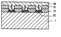
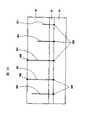
如图1a所示,去除衬底1,由此形成诸如带形、或网格状结构的岛状结构,从而提供一个沟槽/立柱。接着,形成缓冲层2。下面将参照图1b描述包括主要形成在衬底1上的立柱上表面上的部分21和形成在沟槽底面上的部分22的缓冲层2的示例。As shown in Figure 1a, the
如图1b所示,以包括形成在立柱上表面上的部分21和形成在衬底1的沟槽底面上的部分22的缓冲层2作为晶体生长的籽晶,III族氮化物系化合物半导体3垂直并横向外延生长,衬底1具有诸如带形或网格状结构的岛状结构的沟槽。然后,如图1c所示,以形成在立柱上表面上的缓冲层21作用为晶体生长的籽晶或晶核,III族氮化物系化合物半导体31可以在从沟槽底面上形成的缓冲层22上生长的III族氮化物系化合物半导体32填埋沟槽之前覆盖沟槽的上部。此外,通过垂直或横向的外延生长III族氮化物系化合物半导体3,衬底沟槽的上部被如图1d所示的外延生长所覆盖,且在垂直方向扩散的线位错的密度被显著降低。As shown in FIG. 1b, a
当自立柱或台地上表面上形成的缓冲层21横向外延生长的III族氮化物系化合物半导体31会合到从立柱的彼此面对的上表面起始的横向外延生长层的速率快于自沟槽底面上形成的缓冲层22沿垂直方向外延生长的III族氮化物系化合物半导体32生长到立柱上层的速率时,从沟槽底层上形成的缓冲层22扩散的线位错在如此填埋的III族氮化物系化合物半导体31的上部内得以显著抑制,由此提供了明显高质量的结晶区。在这种情况下,如图1d所示,自作为晶体生长的籽晶的形成在沟槽底部上的缓冲层22生长的III族氮化物系化合物半导体32的生长前沿未暴露在表面上,而作为空腔保留。并且,在空腔上方,自两侧的立柱的上层上形成的并作用为晶体生长的籽晶的缓冲层生长的III族氮化物系化合物半导体31的生长前沿会合。线位错自缓冲层22的扩散可以在空腔处得以防止。When the Group III
在图1b中,缓冲层难于形成在衬底1的沟槽侧壁上。接着,下面将描述当缓冲层如图2a~2d所示形成在衬底1的沟槽侧壁上的情况。如图1a所示,沟槽/立柱通过蚀刻衬底1(图2a)而形成。然后,如图2b所示,以缓冲层2作为晶体生长的籽晶,III族氮化物系化合物半导体3垂直并横向外延生长,该缓冲层形成在衬底1的立柱上表面、沟槽下表面和沟槽侧壁上,该沟槽形成为具有岛状结构,如点状、带形或网格状结构。如图2c所示,自沟槽底面和侧壁处的缓冲层2沿垂直方向外延生长的III族氮化物系化合物半导体3填埋沟槽,并且自缓冲层2的立柱上表面生长的III族氮化物系化合物半导体3沿着横向生长,从而覆盖沟槽。在此,自沟槽侧壁的“在垂直方向生长”意味着在垂直于沟槽侧壁的方向上生长。然后,如图1d所示,衬底的沟槽上部由自沟槽侧壁上形成的缓冲层2垂直生长并填埋沟槽的III族氮化物系化合物半导体3,和自形成在立柱上表面的缓冲层2横向生长的III族氮化物系化合物半导体3占据。在沟槽侧壁上形成的缓冲层2上垂直生长的在垂直方向的III族氮化物系化合物半导体3中的线位错处于沟槽侧壁的法向上,而从衬底表面(立柱上表面和沟槽底面)沿着垂直方向扩散的线位错的密度得以极度减弱。In FIG. 1b , the buffer layer is difficult to form on the trench sidewall of the
当自立柱上表面上形成的缓冲层横向外延生长的III族氮化物系化合物半导体3与从沟槽底面上形成的缓冲层2沿垂直方向外延生长的III族氮化物系化合物半导体3向立柱上层生长相比更快速会合时,在如此填埋的III族氮化物系化合物半导体3的上部内自缓冲层2的线位错扩散得以显著抑制,由此提供了明显高质量的结晶区。在这种情况下,如图2d所示,自用作晶体生长籽晶的沟槽底面上的缓冲层2生长的III族氮化物系化合物半导体3的生长前沿不从表面上出来,而是继续保持为空腔。并且在该空腔上方,自作用为晶体生长的籽晶的立柱上的缓冲层2生长的III族氮化物系化合物半导体3的生长前沿会合,且通过这个空腔防止了自沟槽底面上的缓冲层2扩散的线位错。When the group III
当III族氮化物系化合物半导体31采取{11-20}面作为沟槽侧壁的生长前沿时,上述的快速横向外延生长可以轻易实现。在横向外延生长过程中,至少生长前沿的上部可以优选地保持一个{11-20}面。当然,横向外延生长前沿不能局限于III族氮化物系化合物半导体的{11-20}面。When the III-
上述过程可以应用于不是在缓冲层上,而是直接在衬底上外延生长的III族氮化物系化合物半导体。图3a~3c图示了如下过程,即,去除衬底1的一部分从而形成沟槽(图3a),垂直并横向生长III族氮化物系化合物半导体3(图3b),以及以III族氮化物系化合物半导体3作用为晶体生长的籽晶,通过形成于立柱上表面上的一部分的横向生长覆盖沟槽(图3c)。且如图4a~4d所示,III族氮化物系化合物半导体的单晶层3(作为立柱上层的单晶层31和作为沟槽底层的单晶层32)可以形成在缓冲层2(作为立柱上层的缓冲层21和作为沟槽底层的缓冲层22)上(图4b),由此,以立柱上层的单晶层31作用为晶体生长的籽晶,通过横向生长覆盖沟槽(图4c和图4d)。The above-described process can be applied to a Group III nitride-based compound semiconductor epitaxially grown not on a buffer layer but directly on a substrate. 3a to 3c illustrate the process of removing part of the
[根据第四和第五特征的发明][Inventions according to the fourth and fifth features]
如图5a所示,缓冲层2形成在衬底1上。然后,如图5b所示,去除缓冲层2和衬底1的部分,从而提供沟槽/立柱。如图5c所示,主要以缓冲层2作用为晶体生长的籽晶,III族氮化物系化合物层31垂直并横向外延生长。图5c示出了自立柱/沟槽的底面和侧壁外延生长的III族氮化物系化合物半导体32。当自立柱上表面上形成的缓冲层2沿着横向外延生长的III族氮化物系化合物半导体31会合到起始于立柱的彼此面对的上表面的横向外延生长前沿的速率快于自沟槽底面和侧壁上形成的缓冲层2沿垂直方向外延生长的III族氮化物系化合物半导体32生长到立柱上层的速率时,自沟槽底层扩散的线位错在如此填埋的III族氮化物系化合物半导体31的上部内得以显著抑制,由此提供了明显高质量的结晶区。在这种情况下,如图5d所示,自作用为晶体生长的籽晶的沟槽底部上所形成的缓冲层2生长的III族氮化物系化合物半导体32的生长层不暴露在表面处,而是继续作为空腔。并且在该空腔上方,自形成在两侧立柱上层上并作用为晶体生长的籽晶的缓冲层2生长的III族氮化物系化合物半导体31的生长前沿会合。在空腔处可以防止线位错从缓冲层2扩散。As shown in FIG. 5 a ,
当平行于沟槽侧壁的III族氮化物系化合物半导体层31的生长前沿呈现{11-20}面时,上述快速横向外延生长可以轻易实现。在横向外延生长过程中,至少生长前沿的上部可以优选地保持{11-20}面。当然,横向外延生长前沿不能局限于III族氮化物系化合物半导体的{11-20}面。When the growth front of the III-nitride-based
如图6a~6d所示,形成了缓冲层2和III族氮化物系化合物半导体31的单晶层31(图6a),形成了沟槽(图6b),由此以立柱上层的单晶层31作为晶体生长的籽晶,通过横向生长覆盖沟槽(图6c和图6d)。As shown in FIGS. 6a to 6d, the
[根据第六到第八特征的发明][Inventions According to Sixth to Eighth Features]
如图7a所示,例如通过蚀刻或刮擦粗糙化的粗糙部分A形成在衬底1的表面上,从而衬底表面的不粗糙的其他部分变成岛状结构,如带形或网格状结构。然后,缓冲层2形成在衬底1上。与形成在表面不粗糙部分上的缓冲层21相比,形成在衬底表面粗糙部分A上的缓冲层22的表面层不能成为均匀的单晶层,且此外其生长速度非常缓慢(图7b)。当III族氮化物系化合物半导体3在其上垂直并横向外延生长时,以主要形成在衬底1的表面未粗糙化的部分上的缓冲层21作为晶体生长的籽晶,快速形成单晶层,且形成在粗糙部分A上的缓冲层22也通过横向生长而得以覆盖(图7c)。通过进一步在垂直和横向上外延生长III族氮化物系化合物半导体3,形成在粗糙部分A上的缓冲层22被以主要形成在表面上未粗糙化部分上的缓冲层21作为晶体生长的籽晶而横向外延生长的III族氮化物系化合物半导体3完全覆盖。在这种情况下,自粗糙部分A上形成的缓冲层22产生的垂直方向上的线位错不会扩散到沿着横向外延生长的III族氮化物系化合物半导体3上。As shown in FIG. 7a, a rough portion A roughened, for example, by etching or scraping is formed on the surface of the
如图8a所示,例如通过蚀刻和蚀刻或刮擦粗糙化的粗糙部分A形成在衬底1的表面上,从而不粗糙的衬底表面的其他部分变成岛状结构,如带形或网格状结构。然后,在衬底1上外延生长的III族氮化物系化合物半导体3形成于其上。与形成在表面不粗糙部分上的III族氮化物系化合物半导体31相比,形成在衬底表面粗糙部分A上的III族氮化物系化合物半导体32内的表面层不能成为均匀的单晶层,且其生长速度相当缓慢(图8b)。通过垂直和横向进一步外延生长III族氮化物系化合物半导体3,形成在粗糙部分A上的III族氮化物系化合物半导体32的上部完全由横向外延生长的III族氮化物系化合物半导体31覆盖。在这种情况下,自形成在粗糙部分A上的III族氮化物系化合物半导体32产生的垂直方向上的线位错不会扩散到其上横向外延生长的III族氮化物系化合物半导体31上。As shown in FIG. 8a, a rough portion A roughened, for example, by etching and etching or scraping is formed on the surface of the
在图7a~7d中,在衬底1上只有单独一个III族氮化物系化合物半导体3垂直并横向外延生长。此外,如图9a~9d所示,缓冲层21形成在表面未粗糙化的部分上,III族氮化物系化合物半导体31在缓冲层21上沿垂直方向生长,作用为单晶层,而III族氮化物系化合物半导体32可以以III族氮化物系化合物半导体的单晶层31作为晶体生长的籽晶而沿垂直和横向方向在其上生长。In FIGS. 7 a to 7 d , only a single III-nitride-based
[根据第九和第十特征的发明][Inventions according to ninth and tenth features]
如图10a~10d所示,在衬底1上形成缓冲层2(图10a)和通过蚀刻或刮擦损坏其表面(图10b)之后,III族氮化物系化合物半导体3可以沿垂直和横向方向在其上生长(图10c和10d)。如图11a~11d所示,在衬底1上形成缓冲层2和III族氮化物系化合物半导体31(图11a)并通过蚀刻或刮擦损坏其表面(图11b)之后,III族氮化物系化合物半导体层33可以沿垂直和横向方向生长于其上(图11c和11d)。形成在表面未粗糙化部分上的III族氮化物系化合物半导体层比形成在衬底粗糙部分上的生长更快,如图10c和11c所示。通过其以形成在表面未粗糙化部分上的部分作为晶体生长的籽晶沿横向生长III族氮化物系化合物半导体层,该层生长成覆盖带有粗糙表面的部分。As shown in FIGS. 10a to 10d, after forming the
通过如上所述的过程,可以提供其中线位错在垂直方向扩散的III族氮化物系化合物半导体。Through the process as described above, a group III nitride-based compound semiconductor in which thread dislocations diffuse in the vertical direction can be provided.
通过在III族氮化物系化合物半导体层的一部分上形成作为上层的器件元件,可以提供一种具有包含较少缺陷的层并被赋予了较高迁移率的半导体器件,其中III族氮化物系化合物半导体层是通过上述步骤横向外延生长而形成的(第十一特征)。By forming a device element as an upper layer on a part of a group III nitride compound semiconductor layer, it is possible to provide a semiconductor device having a layer containing fewer defects and endowed with higher mobility, in which the group III nitride compound semiconductor layer The semiconductor layer is formed by lateral epitaxial growth through the above steps (eleventh feature).
通过将作为上层的发光元件叠置在通过上述步骤形成的III族氮化物系化合物半导体层上,可以提供一种寿命得以提高且LD阈值得以改善的发光器件(第十二特征)。By stacking a light-emitting element as an upper layer on the group III nitride-based compound semiconductor layer formed by the above steps, a light-emitting device with improved lifetime and improved LD threshold can be provided (twelfth feature).
通过从其他层选择性地分离形成在通过上述步骤横向外延生长而提供的III族氮化物系化合物半导体层一部分上的上层,可以产生一种高结晶度的III族氮化物系化合物半导体,其中,诸如位错之类的晶体缺陷得以明显抑制(第十三特征)。在这方面,为了制造方便的缘故,“基本上去除整个部分”的表达方式并未排除包含线位错的部分在一定程度上存在的情况。By selectively separating the upper layer formed on a part of the group III nitride-based compound semiconductor layer provided by the lateral epitaxial growth in the above step from other layers, a highly crystalline group III nitride-based compound semiconductor can be produced, wherein, Crystal defects such as dislocations are remarkably suppressed (thirteenth feature). In this regard, the expression "substantially the entire portion is removed" does not exclude the case where a portion containing thread dislocations exists to some extent for the sake of manufacturing convenience.
附图说明Description of drawings
图1是一系列剖面图,示出了制造根据本发明第一实施例的III族氮化物系化合物半导体的步骤;1 is a series of sectional views showing steps of manufacturing a group III nitride-based compound semiconductor according to a first embodiment of the present invention;
图2是一系列剖面图,示出了制造本发明的另一种III族氮化物系化合物半导体的步骤;2 is a series of cross-sectional views showing the steps of manufacturing another III-nitride-based compound semiconductor of the present invention;
图3是一系列剖面图,示出了制造根据本发明第七实施例的III族氮化物系化合物半导体的步骤;3 is a series of cross-sectional views showing steps of manufacturing a Group III nitride-based compound semiconductor according to a seventh embodiment of the present invention;
图4是一系列剖面图,示出了制造本发明的另一种III族氮化物系化合物半导体的步骤;4 is a series of cross-sectional views showing the steps of manufacturing another III-nitride-based compound semiconductor of the present invention;
图5是一系列剖面图,示出了制造根据本发明第二实施例的III族氮化物系化合物半导体发光器件的步骤;5 is a series of cross-sectional views showing the steps of manufacturing a Group III nitride-based compound semiconductor light-emitting device according to a second embodiment of the present invention;
图6是一系列剖面图,示出了制造本发明的另一种III族氮化物系化合物半导体的步骤;6 is a series of cross-sectional views showing the steps of manufacturing another III-nitride-based compound semiconductor of the present invention;
图7是一系列剖面图,示出了制造根据本发明第三实施例的III族氮化物系化合物半导体的步骤;7 is a series of cross-sectional views showing steps of manufacturing a group III nitride-based compound semiconductor according to a third embodiment of the present invention;
图8是一系列剖面图,示出了制造本发明的另一种III族氮化物系化合物半导体的步骤;8 is a series of cross-sectional views showing the steps of manufacturing another III-nitride-based compound semiconductor of the present invention;
图9是一系列剖面图,示出了制造本发明另一种不同的III族氮化物系化合物半导体的步骤;9 is a series of cross-sectional views showing the steps of manufacturing another different group III nitride-based compound semiconductor of the present invention;
图10是一系列剖面图,示出了制造本发明另一种不同的III族氮化物系化合物半导体的步骤;10 is a series of cross-sectional views showing the steps of manufacturing another different group III nitride-based compound semiconductor of the present invention;
图11是是一系列剖面图,示出了制造本发明另一种不同的III族氮化物系化合物半导体的步骤;11 is a series of cross-sectional views showing the steps of manufacturing another different group III nitride compound semiconductor of the present invention;
图12是一系列剖面图,示出了制造根据本发明第四实施例的III族氮化物系化合物半导体的步骤;12 is a series of cross-sectional views showing steps of manufacturing a group III nitride-based compound semiconductor according to a fourth embodiment of the present invention;
图13是一系列剖面图,示出了制造根据本发明第五实施例的III族氮化物系化合物半导体发光器件的步骤;13 is a series of cross-sectional views showing the steps of manufacturing a Group III nitride-based compound semiconductor light-emitting device according to a fifth embodiment of the present invention;
图14是示出根据本发明第六实施例的一种III族氮化物系化合物半导体发光器件的剖面图;14 is a cross-sectional view showing a Group III nitride-based compound semiconductor light-emitting device according to a sixth embodiment of the present invention;
图15是示出根据本发明第七实施例的一种III族氮化物系化合物半导体发光器件的剖面图;15 is a cross-sectional view showing a Group III nitride-based compound semiconductor light-emitting device according to a seventh embodiment of the present invention;
图16是示出根据本发明第八实施例的一种III族氮化物系化合物半导体发光器件的剖面图;16 is a cross-sectional view showing a Group III nitride-based compound semiconductor light emitting device according to an eighth embodiment of the present invention;
图17是示出蚀刻第一III族氮化物系化合物半导体的另一示例的示意图;以及17 is a schematic diagram showing another example of etching the first Group III nitride-based compound semiconductor; and
图18是示出在III族氮化物系化合物半导体中扩散的线位错的剖面图。FIG. 18 is a cross-sectional view showing linear dislocations diffused in a Group III nitride-based compound semiconductor.
具体实施方式Detailed ways
下面将参照附图描述本发明各实施例。本发明具有上述特征,且不局限于将具体描述的各实施例。Embodiments of the present invention will be described below with reference to the accompanying drawings. The present invention has the above-mentioned features and is not limited to the embodiments that will be specifically described.
图1~8中每幅图示出了实施本发明的制造III族氮化物系化合物半导体的方法的模式。图1示出其中衬底1的切割的侧壁上不形成缓冲层2的示例。通过切割衬底1形成沟槽(图1a),形成缓冲层(图1b),且III族氮化物系化合物半导体层3沿横向外延生长(图1c)。图1a中所示的切割的宽度和深度确定成使得III族氮化物系化合物半导体层31在III族氮化物系化合物半导体层32如上所述填埋沟槽之前覆盖沟槽的上部,其中,III族氮化物系化合物半导体层31是以形成在立柱或台地上表面上的缓冲层21作为晶体生长的籽晶或晶核而垂直并横向生长的,而III族氮化物系化合物半导体层32是以形成在沟槽底面上的缓冲层2作为晶体生长的籽晶而垂直生长的。在图1c中,横向外延生长前沿例如采取{11-20}面。但是在本发明中,其不限制生长前沿表面的取向。于是,切割的形式和横向外延生长条件确定为使得III族氮化物系化合物半导体层31以形成在立柱上表面上的缓冲层21作为晶体生长的籽晶的横向生长在自沟槽底面的垂直生长填埋切割部分之前在通过切割形成的沟槽上部会合,由此线位错在通过切割获得的沟槽上部上形成的III族氮化物系化合物半导体层31的区域内被抑制(图1d)。Each of FIGS. 1 to 8 shows a mode of carrying out the method of manufacturing a group III nitride-based compound semiconductor of the present invention. FIG. 1 shows an example in which
图2示出当缓冲层2也形成在沟槽每个侧壁上时的结构。其他将产生的效果与参照图1的情况在前面描述的效果相同。FIG. 2 shows the structure when the
图5示出在衬底1上形成缓冲层2之后进行切割的实施例。没有缓冲层2,形成在衬底1上的沟槽的底面和侧壁不会垂直生长,或以极其缓慢的速度生长。以形成在立柱上表面上的缓冲层2作为晶体生长的籽晶的横向生长覆盖通过切割形成的沟槽(图5c和5d)。如上所述,图2a所示的切割的宽度和深度确定为使得以形成在立柱上表面上的缓冲层21作为晶体生长的籽晶的III族氮化物系化合物半导体层31的横向生长在III族氮化物系化合物半导体层32自沟槽底面的垂直生长填埋切割部分之前覆盖沟槽的上部。在图2c中,横向外延生长前沿例如采取{11-20}面。但是在本发明中,其并不限制生长前沿表面的取向。FIG. 5 shows an embodiment in which dicing is performed after the
图7示出在使衬底1表面粗糙后形成缓冲层2的方式。粗糙部分A的面积确定为使得III族氮化物系化合物半导体层3以形成在衬底1表面未粗糙化部分上的缓冲层21作为晶体生长的籽晶在垂直和横向外延生长,并覆盖形成在粗糙部分A上的缓冲层22,该缓冲层的表面层不能成为均匀的单晶层,且该缓冲层生长速度较低。FIG. 7 shows the manner in which
图8示出在使衬底1的表面粗糙之后直接形成III族氮化物系化合物半导体的方式。粗糙部分A的面积确定为使得形成在衬底1的表面的未粗糙化部分上的III族氮化物系化合物半导体层31在垂直方向和横向外延生长,并覆盖形成在粗糙部分A上的III族氮化物系化合物半导体层32,后者的表面层不能成为均匀的单晶层,且后者生长速度较低。FIG. 8 shows a manner in which a Group III nitride-based compound semiconductor is directly formed after roughening the surface of the
实施本发明的上述方式允许如下面所述进行选择。The above-described modes of carrying out the invention allow for selection as described below.
当要形成包括衬底和III族氮化物系化合物半导体的叠片时,衬底可以为蓝宝石、硅(Si)、碳化硅(SiC)、尖晶石(MgAl2O4)、ZnO、MgO等的无机晶体衬底,且可以使用III-V族化合物半导体,如磷化镓或砷化镓半导体,或III族氮化物系化合物半导体,如氮化镓(GaN)半导体。When forming a laminate including a substrate and a III-nitride compound semiconductor, the substrate can be sapphire, silicon (Si), silicon carbide (SiC), spinel (MgAl2 O4 ), ZnO, MgO, etc. Inorganic crystal substrates, and can use III-V group compound semiconductors, such as gallium phosphide or gallium arsenide semiconductors, or group III nitride-based compound semiconductors, such as gallium nitride (GaN) semiconductors.
形成III族氮化物系化合物半导体层的优选方法为金属有机化学气相沉积(MOCVD)或金属有机气相外延生长(MOVPE)。然而,可以使用分子束外延(MBE)、卤化物气相外延(halide VPE)、液相外延(LPE)等。并且,可以通过不同的生长方法形成各层。A preferred method of forming the III-nitride-based compound semiconductor layer is metal organic chemical vapor deposition (MOCVD) or metal organic vapor phase epitaxy (MOVPE). However, molecular beam epitaxy (MBE), halide vapor phase epitaxy (halide VPE), liquid phase epitaxy (LPE), or the like may be used. Also, each layer may be formed by a different growth method.
当III族氮化物系化合物半导体层要形成在例如蓝宝石衬底上时,为了给该层赋予较好的结晶度,为了校正与蓝宝石衬底的晶格失配的目的,优选地形成缓冲层。当使用另一种材料的衬底时,采用缓冲层也是优选的。缓冲层优选的为低温形成的III族氮化物系化合物半导体AlxGayIn1-x-yN(0≤x≤1,0≤y≤1,0≤x+y≤1),更优选地为AlxGa1-xN(0≤x≤1)。这种缓冲层可以为单层或包括不同成份的多成份层。缓冲层可以在380~420℃的低温下形成,或在1000~1180℃下通过MOCVD形成。另外,AlN缓冲层可以通过利用DC磁控溅射装置的反应溅射方法形成,作为材料,可以使用高纯度的铝和氮气。类似地,可以形成由分子式AlxGayIn1-x-yN(0≤x≤1,0≤y≤1,0≤x+y≤1,任意组成)表示的缓冲层。此外,可以采用气相沉积、离子镀、激光磨蚀或ECR。当缓冲层要通过物理气相沉积形成时,物理气相沉积优选地在200~600℃,更优选地在300~500℃,最优选地在350~450℃下进行。当采用诸如溅射的物理气相沉积时,缓冲层的厚度优选地为100~3000埃,更优选地为100~500埃,最优选地为100~300埃。作为横向外延生长的籽晶的III族氮化物系化合物半导体层和/或III族氮化物系化合物半导体的上层可以为包括重复的缓冲层单元的层(底层),并可以形成单晶III族氮化物系化合物半导体层。底层最优选地可以包括作为最上层的单晶层,其可以作用为横向外延生长的籽晶。When a Group III nitride-based compound semiconductor layer is to be formed on, for example, a sapphire substrate, in order to impart better crystallinity to the layer, for the purpose of correcting lattice mismatch with the sapphire substrate, it is preferable to form a buffer layer. It is also preferable to use a buffer layer when a substrate of another material is used. The buffer layer is preferably a group III nitride compound semiconductor Alx Gay In1-xy N (0≤x≤1, 0≤y≤1, 0≤x+y≤1) formed at low temperature, more preferablyAlxGa1-xN (0≤x≤1). This buffer layer can be a single layer or a multi-component layer comprising different components. The buffer layer may be formed at a low temperature of 380˜420° C., or by MOCVD at 1000˜1180° C. In addition, the AlN buffer layer can be formed by a reactive sputtering method using a DC magnetron sputtering device, and high-purity aluminum and nitrogen gas can be used as materials. Similarly, a buffer layer represented by the molecular formulaAlxGayIn1-xyN (0≤x≤1, 0≤y≤1, 0≤x+y≤1, arbitrary composition) can be formed. In addition, vapor deposition, ion plating, laser abrasion, or ECR may be employed. When the buffer layer is to be formed by physical vapor deposition, the physical vapor deposition is preferably performed at 200 to 600°C, more preferably at 300 to 500°C, most preferably at 350 to 450°C. When using physical vapor deposition such as sputtering, the thickness of the buffer layer is preferably 100-3000 angstroms, more preferably 100-500 angstroms, most preferably 100-300 angstroms. The Group III nitride-based compound semiconductor layer as a seed crystal for lateral epitaxial growth and/or the upper layer of the Group III nitride-based compound semiconductor may be a layer (underlayer) including repeated buffer layer units, and may form a single crystal Group III nitrogen compound semiconductor layer. The bottom layer may most preferably comprise, as the uppermost layer, a single crystal layer, which may act as a seed for lateral epitaxial growth.
即使在缓冲层、作用为横向外延生长的籽晶的III族氮化物系化合物半导体层、横向外延生长的层、以及/或位于上表面的III族氮化物系化合物半导体的组成成为使得一部分III族元素由硼(B)或铊(Tl)替代或者一部分氮(N)原子由磷(P)、砷(As)、锑(Sb)、或铋(Bi)替代时,本发明也可以充分得以应用。同样,缓冲层和III族氮化物系化合物半导体可以掺杂这些元素中任一种到不在其组成中呈现的程度。例如,由AlxGa1-xN(0≤x≤1)表示且不包含铟(In)和砷(As)的III族氮化物系化合物半导体可以掺杂有铟(In)或砷(As),铟的原子半径大于铝(Al)和镓(Ga),而砷(As)的原子半径大于氮(N),从而通过借助于压缩应变的对由氮原子散去而导致的晶体膨胀应变的补偿而获得改善的结晶度。在这种情况下,由于受主杂质容易占据III族原子的位置,可以随着生长获得p型晶体。通过结晶度的如此实现的改进与本发明的特征相结合,可以进一步将线位错降低到大约1/100到1/1000。在发光器件为目标产品的情况下,使用二元或三元的III族氮化物系化合物半导体是优选的。Even if the composition of the buffer layer, the group III nitride compound semiconductor layer serving as a seed crystal for lateral epitaxial growth, the layer grown laterally, and/or the group III nitride compound semiconductor on the upper surface becomes such that a part of the group III The present invention can also be fully applied when an element is replaced by boron (B) or thallium (Tl), or a part of nitrogen (N) atoms is replaced by phosphorus (P), arsenic (As), antimony (Sb), or bismuth (Bi). . Also, the buffer layer and the Group III nitride-based compound semiconductor may be doped with any of these elements to such an extent that it does not appear in its composition. For example, a Group III nitride-based compound semiconductor represented byAlxGa1-xN (0≤x≤1) and not containing indium (In) and arsenic (As) may be doped with indium (In) or arsenic (As ), the atomic radius of indium is greater than that of aluminum (Al) and gallium (Ga), and that of arsenic (As) is greater than that of nitrogen (N), so that the crystal expansion strain caused by the scattering of nitrogen atoms by means of compressive strain improved crystallinity due to compensation. In this case, p-type crystals can be obtained as the growth occurs since acceptor impurities easily occupy the sites of Group III atoms. By the thus achieved improvement in crystallinity combined with the features of the present invention, it is possible to further reduce the thread dislocation to about 1/100 to 1/1000. In the case where a light-emitting device is the target product, it is preferable to use a binary or ternary Group III nitride-based compound semiconductor.
当形成n型III族氮化物化合物半导体层时,可以加入作为n型杂质的IV族或VI族元素,如Si、Ge、Se、Te或C。II族或IV族元素,如Zn、Mg、Be、Ca、Sr或Ba可以作为p型杂质加入。相同的层可以掺杂多种n型或p型杂质,或掺杂n型和p型杂质二者。When forming the n-type group III nitride compound semiconductor layer, a group IV or group VI element such as Si, Ge, Se, Te or C may be added as an n-type impurity. Group II or IV elements such as Zn, Mg, Be, Ca, Sr or Ba may be added as p-type impurities. The same layer can be doped with multiple n-type or p-type impurities, or with both n-type and p-type impurities.
优选地是,横向外延生长前沿垂直于衬底。然而,横向外延生长可以在保持相对于衬底的倾斜小面(facet)的同时进行。Preferably, the lateral epitaxial growth front is perpendicular to the substrate. However, lateral epitaxial growth can be performed while maintaining an inclined facet relative to the substrate.
优选地是,横向外延生长进行为至少横向外延生长前沿的上部垂直于衬底表面。更优选的是,生长前沿为III族氮化物系化合物半导体的{11-20}面。Preferably, the lateral epitaxial growth proceeds with at least an upper portion of the lateral epitaxial growth front perpendicular to the substrate surface. More preferably, the growth front is the {11-20} plane of the Group III nitride compound semiconductor.
要蚀刻的沟槽的深度和宽度确定为使得横向外延生长填充沟槽。在利用至少在生长初始阶段不发生自衬底表面或自不同层的垂直生长或生长非常缓慢的现象的同时确定蚀刻的条件。The depth and width of the trenches to be etched are determined such that the lateral epitaxial growth fills the trenches. Conditions of etching are determined while utilizing a phenomenon that vertical growth from the substrate surface or from different layers does not occur or growth is very slow at least in the initial stage of growth.
当要形成在衬底上的III族氮化物系化合物半导体层的晶体取向可以预测时,掩蔽或切割以平行于III族氮化物系化合物半导体层的a面({11-20}面)或m面({1-100}面)的条带形式形成在衬底上的沟槽的侧壁是有利的。上述条带或掩模图案可以为岛状或网格状,或者可以呈现其他形式。横向外延生长的前沿可以垂直于或倾斜于衬底表面。为了使III族氮化物系化合物半导体层的a面,即{11-20}面变成横向外延生长前沿,条带的纵向例如必须垂直于III族氮化物系化合物半导体层的m面,即{1-100}面。例如,当衬底表面为蓝宝石的a面或c面时,蓝宝石的m面通常匹配衬底上形成的III族氮化物系化合物半导体层的a面。从而,切割按照各面的排列予以进行。在点状、网格状或岛状蚀刻情况下,限定外廓(侧壁)的面优选地为形成为上层的III族氮化物系化合物半导体层的{11-20}面。When the crystal orientation of the group III nitride compound semiconductor layer to be formed on the substrate can be predicted, masking or cutting so as to be parallel to the a plane ({11-20} plane) or m of the group III nitride compound semiconductor layer It is advantageous to form the sidewalls of the trenches on the substrate in stripes of planes ({1-100} planes). The above strip or mask pattern may be in the shape of islands or grids, or may be in other forms. The front of lateral epitaxial growth can be perpendicular or inclined to the substrate surface. In order to make the a-plane of the III-nitride-based compound semiconductor layer, that is, the {11-20} plane become the lateral epitaxial growth front, the longitudinal direction of the strip must be perpendicular to the m-plane of the III-nitride-based compound semiconductor layer, ie { 1-100} surface. For example, when the substrate surface is the a-plane or c-plane of sapphire, the m-plane of sapphire usually matches the a-plane of the Group III nitride-based compound semiconductor layer formed on the substrate. Thus, cutting is performed according to the arrangement of the faces. In the case of dot-like, grid-like or island-like etching, the plane defining the outline (sidewall) is preferably the {11-20} plane of the Group III nitride-based compound semiconductor layer formed as the upper layer.
蚀刻掩模可以包括氧化物或氮化物,如氧化硅(SiO2)、氮化硅(Si3N4)、氧化钛(TiOx)、或氧化锆(ZrOx);或可以呈现其多层薄膜的形式。蚀刻掩模可以通过如气相沉积、溅射或CVD的气相生长方法或其他方法形成。The etch mask may comprise an oxide or nitride such as silicon oxide (SiO2 ), silicon nitride (Si3 N4 ), titanium oxide (TiOx ), or zirconium oxide (ZrOx ); or may exhibit multiple layers thereof film form. The etching mask may be formed by a vapor growth method such as vapor deposition, sputtering, or CVD, or other methods.
反应粒子束蚀刻(RIE)是优选的,但是可以采用任何其他的蚀刻方法。替换蚀刻的是,沟槽可以通过利用机械加工形成,如可以利用刮擦。其他任意方法,例如利用金刚石刀具的刮擦也可以用于使衬底粗糙化。Reactive beam etching (RIE) is preferred, but any other etching method may be used. Instead of etching, trenches can be formed by using mechanical working, eg scraping can be used. Any other method, such as scraping with a diamond tool, can also be used to roughen the substrate.
诸如FET或发光器件的半导体器件可以在上述具有抑制线位错的区域的III族氮化物化合物半导体上遍及整个区域或主要在线位错得以抑制的区域上形成。在发光器件情况下,发光层采取多量子阱(MQW)结构、单量子阱(SQW)结构、同质结构、单异质结构、或双异质结构,或者可以例如借助于pin节或pn节形成。A semiconductor device such as a FET or a light emitting device can be formed over the entire region or mainly on the region where the linear dislocation is suppressed on the above-mentioned group III nitride compound semiconductor having the region where the linear dislocation is suppressed. In the case of a light-emitting device, the light-emitting layer adopts a multi-quantum well (MQW) structure, a single quantum well (SQW) structure, a homostructure, a single heterostructure, or a double heterostructure, or can be e.g. form.
上述具有抑制线位错区域的III族氮化物系化合物半导体可以例如通过去除衬底1、缓冲层2和III族氮化物系化合物半导体的未抑制线位错部分而形成为III族氮化物系化合物衬底。如此形成的衬底可以允许III族氮化物系化合物半导体器件在其上形成,或者可以用作用于形成更大的III族氮化物系化合物半导体晶体的衬底。所述去除可以通过机械化学抛光或者任何其他适当的方法进行。The above-mentioned group III nitride-based compound semiconductor having a region for suppressing thread dislocation can be formed into a group III nitride-based compound semiconductor by, for example, removing the
在处理衬底并形成带有较少线位错的区域之后,带有较少线位错的区域形成在具有较多线位错的区域的上部上。这作为可选示例也包括在本发明中。例如,根据本发明第一到第四特征,掩模形成在具有较多线位错的区域上,这些位错形成在包括具有较少线位错的区域和具有较多线位错的区域的III族氮化物系化合物半导体层中。然后以其上未形成掩模的具有较少线位错区域的表面作为晶体生长的籽晶,沿横向外延生长III族氮化物系化合物半导体层,并覆盖掩模的上部,由此获得具有普遍较少线位错的III族氮化物系化合物半导体层。作为另一种替换,可以进行在带有较多线位错的区域的上部上的第二横向外延生长。After processing the substrate and forming the region with fewer thread dislocations, the region with less thread dislocations is formed on top of the region with more thread dislocations. This is also included in the present invention as an optional example. For example, according to the first to fourth features of the present invention, the mask is formed on regions having more thread dislocations formed on regions including the region having fewer thread dislocations and the region having more thread dislocations. In the Group III nitride compound semiconductor layer. Then, using the surface with less linear dislocation regions on which no mask is formed as a seed crystal for crystal growth, a group III nitride-based compound semiconductor layer is epitaxially grown in the lateral direction, and covers the upper part of the mask, thereby obtaining a universal A Group III nitride-based compound semiconductor layer having fewer linear dislocations. As another alternative, a second lateral epitaxial growth on the upper part of the region with more linear dislocations can be performed.
下面将参照具体实施例描述本发明。各实施例将在描述制造发光器件的方法的同时予以说明。然而,本发明不局限于下面描述的实施例。本发明公开了一种制造III族氮化物系化合物半导体的方法,该方法可以应用于任何器件的制造中。The present invention will be described below with reference to specific examples. Each embodiment will be explained while describing a method of manufacturing a light emitting device. However, the present invention is not limited to the embodiments described below. The invention discloses a method for manufacturing group III nitride compound semiconductors, which can be applied to the manufacture of any device.
在下面描述的所有实施例中,本发明的III族氮化物系化合物半导体通过金属有机气相外延(以下称为MOVPE)制造。所使用的典型气体包括氨气(NH3)、载气(H2或N2)、三甲基镓(Ga(CH3)3,以下称为TMG)、三甲基铝(Al(CH3)3,以下称为TMA)、三甲基铟(In(CH3)3,以下称为TMI)、以及环戊二烯基镁((Mg(C5H5)2,以下称为Cp2Mg)。In all the examples described below, the Group III nitride-based compound semiconductor of the present invention was produced by metal-organic vapor phase epitaxy (hereinafter referred to as MOVPE). Typical gases used include ammonia (NH3 ), carrier gas (H2 or N2 ), trimethylgallium (Ga(CH3 )3 , hereinafter referred to as TMG), trimethylaluminum (Al(CH3 )3 , hereinafter referred to as TMA), trimethylindium (In(CH3 )3 , hereinafter referred to as TMI), and cyclopentadienyl magnesium ((Mg(C5 H5 )2 , hereinafter referred to as Cp2 Mg).
[第一实施例][first embodiment]
制备单晶蓝宝石衬底1,使得通过有机净化和热处理而净化的其a面作用为其主表面。通过进行切割,分别为宽度10μm且深度10μm的沟槽以10μm的间隔形成为条带图案。接着,温度设定为400℃,且提供H2(10L/min)、NH3(5L/min)、和TMA(20μmol/min)大约3分钟,从而在蓝宝石衬底1上形成AlN的缓冲层2,该缓冲层2厚度大约为40nm。缓冲层2主要形成在衬底1的沟槽的上表面和底面上。Single
接着,在蓝宝石衬底1的温度保持在1150℃的同时,引入H2(20L/min)、NH3(10L/min)、和TMA(5μmol/min),由此通过垂直和横向外延生长形成GaN层3。此时,自主要形成在立柱上表面上的缓冲层21的横向外延生长填充沟槽,并由此形成平坦的顶面(图1c)。随后,引入H2(20L/min)、NH3(10L/min)、和TMG(300μmol/min),由此生长GaN层3,使得GaN层3的厚度变成10μm。与形成在立柱顶面上的GaN层3的各部分相反,形成在通过衬底1延伸至10μm深的沟槽底部上的GaN层32的各部分具有对线位错的显著抑制。Next, while the temperature of the
[第二实施例][Second embodiment]
制备单晶蓝宝石衬底1,使得通过有机净化和热处理而净化的其a面作用为其主表面。温度下降到400℃,并供给H2(10L/min)、NH3(5L/min)、和TMA(20μmol/min)大约3分钟,由此在蓝宝石衬底1上形成厚度大约为40nm的AlN层(第一缓冲层)2。接着,通过进行切割,分别为宽度10μm、深度10μm的沟槽以10μm的间隔形成为条带图案。缓冲层2仅保留在衬底1的立柱上表面上(图5b)。Single
接着,在蓝宝石衬底1的温度保持在1150℃的同时,引入H2(20L/min)、NH3(10L/min)、和TMG(5μmol/min),由此,通过垂直和横向外延生长形成GaN层3。此时,自主要形成在立柱上表面上的缓冲层2的横向外延生长填充沟槽,并由此形成平坦的顶面(图5c和5d)。随后,引入H2(20L/min)、NH3(10L/min)、和TMG(300μmol/min),由此GaN层31生长来使得GaN层31的厚度为10μm。与GaN层31的形成在立柱顶面上的部分相比,形成在通过衬底1延伸至10μm深的沟槽底部上的部分具有对线位错的显著抑制。Next, while the temperature of the
[第三实施例][Third embodiment]
制备单晶蓝宝石衬底1,使得通过有机净化和热处理而净化的其a面作用为其主表面。然后,衬底1的表面通过反应粒子束蚀刻(RIE)选择性干式蚀刻较短时间,从而具有间隔10μm的带形粗糙部分,该部分宽度为10μm。接着,在蓝宝石衬底1的温度保持在400℃的同时,引入H2(10L/min)、NH3(5L/min)、和TMA(20μmol/min)3分钟,由此形成厚度大约为40nm的AlN缓冲层2。粗糙部分22的表面形态不同于缓冲层2光滑部分21的表面形态(图7b)。Single
接着,在衬底1的温度保持在1150℃的同时,引入H2(20L/min)、NH3(10L/min)、和TMA(5μmol/min),由此通过垂直和横向外延生长形成GaN层3。此时,主要自光滑部分21的横向外延生长覆盖缓冲层2的粗糙部分22,由此获得平坦表面(图7c和7d)。然后,引入H2(20L/min)、NH3(10L/min)、和TMG(300μmol/min),由此形成厚度为3μm的GaN层3。与GaN层3的形成在光滑部分上的部分相反,GaN层3的形成在衬底1上的粗糙部分上的部分呈现出对线位错的显著抑制。Next, while the temperature of the
[第四实施例][Fourth embodiment]
如图12所示,本实施例利用一底层,该底层包括重复的缓冲层和单晶III族氮化物系化合物半导体层。制备单晶蓝宝石衬底1,使得通过有机净化和热处理而净化的其a面作用为其主表面。温度下降到400℃,并供给H2(10L/min)、NH3(5L/min)、和TMA(20μmol/min)大约3分钟,由此在蓝宝石衬底1上形成厚度大约为40nm的第一AlN层2。接着,在蓝宝石衬底1的温度保持在1000℃的同时,引入H2(20L/min)、NH3(10L/min)、和TMG(300μmol/min),由此形成厚度大约为0.3μm的GaN层212。接着,温度下降到400℃,并供给H2(10L/min)、NH3(5L/min)、和TMA(20μmol/min)大约3分钟,由此形成厚度大约为40nm的第二AlN层213。如此形成包括厚度大约为40nm的第一AlN层211、厚度大约为0.3μm的GaN层212和厚度大约为40nm的第二AlN层213的底层20。As shown in FIG. 12, the present embodiment utilizes an underlayer including repeated buffer layers and single crystal Group III nitride-based compound semiconductor layers. Single
接着,以与第二实施例类似的方式,通过切割形成沟槽。使得沟槽延伸到蓝宝石衬底1中10μm深。接着,在蓝宝石衬底1的温度保持在1150℃的同时,引入H2(20L/min)、NH3(10L/min)、和TMG(5μmol/min),由此通过横向外延生长形成GaN层31。横向外延生长是在形成在立柱顶部的底层20作用为晶体生长的籽晶的同时进行的,从而填充沟槽,并因而形成平坦的顶面。随后,引入H2(20L/min)、NH3(10L/min)、和TMG(300μmol/min),由此GaN层31生长来使得GaN层31厚度为10μm。与GaN层31的形成在立柱顶面上的部分相反,GaN层31的形成在沟槽10μm深部分上的部分呈现出对线位错的显著抑制,其中沟槽形成在蓝宝石衬底1中。Next, in a similar manner to the second embodiment, grooves are formed by dicing. The groove was made to extend into the
[第五实施例][Fifth Embodiment]
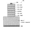
在以与第一实施例类似的方式形成的晶片上,图13所示的激光二极管(LD)100以如下方式形成。特别是,在GaN层3的形成过程中,引入硅烷(SiH4),从而形成作用为GaN层的硅(Si)掺杂的n型GaN层。为了简化描述的目的,附图仅仅示出晶片1000,以总体上表示带沟槽的蓝宝石衬底1、形成在立柱上表面和沟槽底面上的缓冲层2、以及填充沟槽的GaN,以及示出GaN层103,以表示GaN层3的其余部分。On a wafer formed in a similar manner to that of the first embodiment, a laser diode (LD) 100 shown in FIG. 13 is formed as follows. In particular, during the formation of the
在晶片层1000上形成的n型GaN层103上,形成了硅(Si)掺杂的Al0.08Ga0.92N的n包层104、硅(Si)掺杂的GaN的n导引层105、MQW结构的发光层106、镁(Mg)掺杂的GaN的p导引层107、镁(Mg)掺杂的Al0.08Ga0.92N的p包层108、以及镁(Mg)掺杂的GaN的p接触层109,其中晶片层1000包括带沟槽的蓝宝石衬底1、AlN缓冲层2和GaN层3。接着金(Au)电极110A形成在p接触层109上。局部进行蚀刻,直到由两层GaN层和n型GaN层构成的三层GaN层103暴露出来为止。在暴露的GaN层103上,形成铝(Al)电极110B。如此形成的激光二极管(LD)呈现出器件寿命和发光效率的明显提高。On the n-
[第六实施例][Sixth embodiment]
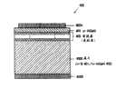
在以与第一实施例类似的方式形成的晶片上,图14所示的发光二极管(LED)200以如下方式形成。在形成GaN层3时,引入硅烷(SiH4),从而GaN层3包括Si掺杂的n型GaN。为了简化说明的缘故,附图仅仅示出了晶片2000,以总体表示带沟槽的蓝宝石衬底1、形成在立柱上表面和沟槽底面上的缓冲层2、以及填充沟槽的GaN层,并且示出了GaN层203,以表示GaN层3的其余部分。On a wafer formed in a similar manner to that of the first embodiment, a light emitting diode (LED) 200 shown in FIG. 14 is formed as follows. When
在形成于晶片层2000上的n型GaN层203上,形成有硅(Si)掺杂的Al0.08Ga0.92N的n包层204、发光层205、镁(Mg)掺杂的Al0.08Ga0.92N的p包层206、以及镁(Mg)掺杂的GaN的p接触层207,其中,晶片层2000包括带沟槽的蓝宝石衬底1、AlN缓冲层2以及填充沟槽的GaN层3。接着,金(Au)电极208A形成在p接触层207上。局部进行蚀刻,直到由GaN层和n型GaN层构成的双层GaN层203暴露出来为止。在暴露的GaN层203上,形成铝(Al)电极208B。如此形成的发光二极管(LED)呈现出器件寿命和发光效率的显著提高。On the n-
[第七实施例][Seventh embodiment]
本实施例利用硅(Si)衬底。Si衬底301蚀刻成条带图案,并且分别为宽10μm、深10μm的沟槽以10μm的间隔形成为条带图案。接着,在硅衬底301的温度保持在1150℃的同时,引入H2(20L/min)、NH3(10L/min)、TMG(5μmol/min)、TMA(0.5μmol/min)和用氢气稀释的硅烷(SiH4)(0.01μmol/min),由此自硅衬底上的沟槽的底面垂直生长n-Al0.15Ga0.85N层,并自硅衬底内立柱的顶面和沟槽的侧壁横向生长n-Al0.15Ga0.85N层。横向外延生长在立柱上部的表面主要用作籽晶的同时进行,由此填充衬底内形成的沟槽,并从而形成平坦的顶面。随后,引入H2(10L/min)、NH3(10L/min)、TMG(100μmol/min)、TMA(10μmol/min)和用氢气稀释的硅烷(SiH4)(0.2μmol/min),由此生长厚度为3μm的n-Al0.15Ga0.85N层。此后,带沟槽的硅衬底301和n-Al0.15Ga0.85N层302由晶片3000概括地表示。This embodiment utilizes a silicon (Si) substrate. The
在晶片3000(带沟槽的硅衬底301和形成在衬底301上的n-Al0.15Ga0.85N层302)上,形成硅(Si)掺杂的GaN的n-导引层303、MQW结构的发光层304、镁(Mg)掺杂的GaN的p-导引层305、镁(Mg)掺杂的Al0.08Ga0.92N的p包层306、以及镁(Mg)掺杂的GaN的p接触层307。接着,金(Au)电极308A形成在p接触层307上,而铝(Al)电极308B形成在硅衬底301的背面上。图15中的如此形成的激光二极管(LD)300呈现出器件寿命和发光效率的显著提高。On the wafer 3000 (a
[第八实施例][Eighth embodiment]
本实施例利用硅(Si)衬底。如利用包括带沟槽的硅衬底301和其上形成的n-Al0.15Ga0.85N层302的晶片的第七实施例一样,本实施例利用包括带沟槽的硅衬底401和衬底401上形成的Al0.15Ga0.85N层402的晶片4000。在晶片4000上,形成发光层403和镁(Mg)掺杂的Al0.15Ga0.85N的p包层404。接着,金(Au)电极405A形成在p包层404上,而铝(Al)电极405B形成在硅衬底401的背面。图16中的如此形成的发光二极管(LED)400呈现出器件寿命和发光效率的明显提高。This embodiment utilizes a silicon (Si) substrate. Like the seventh embodiment using a wafer including a grooved
[蚀刻的改进][Etching improvements]
本实施例允许形成岛状立柱或形成如图17所示的粗糙部分B和光滑部分。为了便于理解,图17a的示意图包括周边区域。实际上,每个晶片可以形成好几千万个岛状立柱,在图17a中,沟槽B底部的面积是岛状立柱顶面的面积的三倍。在图17b中,沟槽B底部的面积是岛状立柱顶面的面积的八倍。This embodiment allows the formation of island-shaped pillars or the formation of rough portions B and smooth portions as shown in FIG. 17 . For ease of understanding, the schematic diagram of Fig. 17a includes a peripheral area. In fact, tens of millions of island-shaped pillars can be formed on each wafer. In FIG. 17a, the area of the bottom of trench B is three times the area of the top surface of the island-shaped pillars. In Fig. 17b, the area of the bottom of trench B is eight times the area of the top of the island-shaped pillar.
虽然本发明已经参照上述实施例加以描述,本发明不局限于此,而是在不背离本发明精髓前提下可以按需要进行改进。Although the present invention has been described with reference to the above-mentioned embodiments, the present invention is not limited thereto but can be modified as required without departing from the gist of the present invention.
本发明所要求优先权的日本专利申请第2000-71350的全部公开物和内容合并于此作为参考。The entire disclosure and content of Japanese Patent Application No. 2000-71350 from which this application claims priority is incorporated herein by reference.
Claims (14)
Translated fromChineseApplications Claiming Priority (3)
| Application Number | Priority Date | Filing Date | Title |
|---|---|---|---|
| JP2000071350AJP2001267242A (en) | 2000-03-14 | 2000-03-14 | Group III nitride compound semiconductor and method of manufacturing the same |
| JP71350/00 | 2000-03-14 | ||
| JP71350/2000 | 2000-03-14 |
Related Parent Applications (1)
| Application Number | Title | Priority Date | Filing Date |
|---|---|---|---|
| CNB018094791ADivisionCN1274008C (en) | 2000-03-14 | 2001-02-23 | Group III nitride compound semiconductor device and manufacturing method thereof |
Publications (2)
| Publication Number | Publication Date |
|---|---|
| CN1624876A CN1624876A (en) | 2005-06-08 |
| CN100461340Ctrue CN100461340C (en) | 2009-02-11 |
Family
ID=18589947
Family Applications (2)
| Application Number | Title | Priority Date | Filing Date |
|---|---|---|---|
| CNB018094791AExpired - LifetimeCN1274008C (en) | 2000-03-14 | 2001-02-23 | Group III nitride compound semiconductor device and manufacturing method thereof |
| CNB2004101021001AExpired - LifetimeCN100461340C (en) | 2000-03-14 | 2001-02-23 | Method for producing group III nitride-based compound semiconductor |
Family Applications Before (1)
| Application Number | Title | Priority Date | Filing Date |
|---|---|---|---|
| CNB018094791AExpired - LifetimeCN1274008C (en) | 2000-03-14 | 2001-02-23 | Group III nitride compound semiconductor device and manufacturing method thereof |
Country Status (7)
| Country | Link |
|---|---|
| US (2) | US6967122B2 (en) |
| EP (1) | EP1265272A4 (en) |
| JP (1) | JP2001267242A (en) |
| KR (2) | KR100623558B1 (en) |
| CN (2) | CN1274008C (en) |
| AU (1) | AU2001234169A1 (en) |
| WO (1) | WO2001069662A1 (en) |
Families Citing this family (113)
| Publication number | Priority date | Publication date | Assignee | Title |
|---|---|---|---|---|
| JP2002008985A (en)* | 2000-06-21 | 2002-01-11 | Nichia Chem Ind Ltd | Method for manufacturing nitride semiconductor and nitride semiconductor substrate |
| JP3556916B2 (en)* | 2000-09-18 | 2004-08-25 | 三菱電線工業株式会社 | Manufacturing method of semiconductor substrate |
| JP4092927B2 (en)* | 2002-02-28 | 2008-05-28 | 豊田合成株式会社 | Group III nitride compound semiconductor, group III nitride compound semiconductor element, and method for manufacturing group III nitride compound semiconductor substrate |
| US7008839B2 (en) | 2002-03-08 | 2006-03-07 | Matsushita Electric Industrial Co., Ltd. | Method for manufacturing semiconductor thin film |
| KR100461238B1 (en)* | 2002-03-09 | 2004-12-14 | 엘지전자 주식회사 | Method for forming GaN epitaxy layer |
| JP3968566B2 (en)* | 2002-03-26 | 2007-08-29 | 日立電線株式会社 | Nitride semiconductor crystal manufacturing method, nitride semiconductor wafer, and nitride semiconductor device |
| US8294172B2 (en)* | 2002-04-09 | 2012-10-23 | Lg Electronics Inc. | Method of fabricating vertical devices using a metal support film |
| US20030189215A1 (en) | 2002-04-09 | 2003-10-09 | Jong-Lam Lee | Method of fabricating vertical structure leds |
| US6841802B2 (en)* | 2002-06-26 | 2005-01-11 | Oriol, Inc. | Thin film light emitting diode |
| JP2004153089A (en) | 2002-10-31 | 2004-05-27 | Toyoda Gosei Co Ltd | Group III nitride compound semiconductor light emitting device and method of manufacturing the same |
| JP2004153090A (en) | 2002-10-31 | 2004-05-27 | Toyoda Gosei Co Ltd | Group III nitride compound semiconductor light emitting device and method of manufacturing the same |
| JP4211358B2 (en)* | 2002-11-01 | 2009-01-21 | 日亜化学工業株式会社 | Nitride semiconductor, nitride semiconductor device and manufacturing method thereof |
| US7524691B2 (en)* | 2003-01-20 | 2009-04-28 | Panasonic Corporation | Method of manufacturing group III nitride substrate |
| KR100504180B1 (en)* | 2003-01-29 | 2005-07-28 | 엘지전자 주식회사 | crystal growth method of nitride compound semiconductor |
| US7276423B2 (en)* | 2003-12-05 | 2007-10-02 | International Rectifier Corporation | III-nitride device and method with variable epitaxial growth direction |
| JP4540347B2 (en)* | 2004-01-05 | 2010-09-08 | シャープ株式会社 | Nitride semiconductor laser device and manufacturing method thereof |
| EP1571241A1 (en)* | 2004-03-01 | 2005-09-07 | S.O.I.T.E.C. Silicon on Insulator Technologies | Method of manufacturing a wafer |
| US7928424B2 (en)* | 2004-03-11 | 2011-04-19 | Epistar Corporation | Nitride-based light-emitting device |
| US9524869B2 (en) | 2004-03-11 | 2016-12-20 | Epistar Corporation | Nitride-based semiconductor light-emitting device |
| US8562738B2 (en) | 2004-03-11 | 2013-10-22 | Epistar Corporation | Nitride-based light-emitting device |
| US7157297B2 (en)* | 2004-05-10 | 2007-01-02 | Sharp Kabushiki Kaisha | Method for fabrication of semiconductor device |
| JP2005322786A (en)* | 2004-05-10 | 2005-11-17 | Sharp Corp | Nitride semiconductor device and manufacturing method thereof |
| US20080163814A1 (en)* | 2006-12-12 | 2008-07-10 | The Regents Of The University Of California | CRYSTAL GROWTH OF M-PLANE AND SEMIPOLAR PLANES OF (Al, In, Ga, B)N ON VARIOUS SUBSTRATES |
| JP4651312B2 (en)* | 2004-06-10 | 2011-03-16 | シャープ株式会社 | Manufacturing method of semiconductor device |
| US20060017064A1 (en)* | 2004-07-26 | 2006-01-26 | Saxler Adam W | Nitride-based transistors having laterally grown active region and methods of fabricating same |
| KR100638609B1 (en) | 2004-08-04 | 2006-10-26 | 삼성전기주식회사 | Nitride semiconductor crystal growth method and nitride semiconductor device manufacturing method |
| CN100365767C (en)* | 2004-09-17 | 2008-01-30 | 同济大学 | A substrate processing method for improving the quality of gallium nitride-based epitaxial layer |
| US7633097B2 (en)* | 2004-09-23 | 2009-12-15 | Philips Lumileds Lighting Company, Llc | Growth of III-nitride light emitting devices on textured substrates |
| KR100580751B1 (en) | 2004-12-23 | 2006-05-15 | 엘지이노텍 주식회사 | Nitride semiconductor light emitting device and manufacturing method |
| CN100435360C (en)* | 2004-12-27 | 2008-11-19 | 北京大学 | Preparation method of LED chip with two-dimensional natural light-scattering surface |
| US10374120B2 (en)* | 2005-02-18 | 2019-08-06 | Koninklijke Philips N.V. | High efficiency solar cells utilizing wafer bonding and layer transfer to integrate non-lattice matched materials |
| US20080035052A1 (en)* | 2005-02-23 | 2008-02-14 | Genesis Photonics Inc. | Method for manufacturing a semiconductor substrate |
| CN1697205A (en)* | 2005-04-15 | 2005-11-16 | 南昌大学 | Method for preparing indium gallium aluminum nitrogen thin film and light-emitting device on silicon substrate |
| JP5364368B2 (en) | 2005-04-21 | 2013-12-11 | エイオーネックス・テクノロジーズ・インコーポレイテッド | Substrate manufacturing method |
| US20060270201A1 (en)* | 2005-05-13 | 2006-11-30 | Chua Soo J | Nano-air-bridged lateral overgrowth of GaN semiconductor layer |
| CN100372137C (en)* | 2005-05-27 | 2008-02-27 | 晶能光电(江西)有限公司 | InGaAlN light-emitting device with upper and lower electrode structure and manufacturing method thereof |
| JP5015440B2 (en)* | 2005-09-29 | 2012-08-29 | 株式会社デンソー | Manufacturing method of semiconductor substrate |
| US20090233414A1 (en)* | 2005-10-20 | 2009-09-17 | Shah Pankaj B | Method for fabricating group III-nitride high electron mobility transistors (HEMTs) |
| CN100474642C (en)* | 2005-10-27 | 2009-04-01 | 晶能光电(江西)有限公司 | Indium gallium aluminium nitrogen semi-conductor luminous element containing metallic chromium substrate and manufacturing method thereof |
| JP2007161525A (en)* | 2005-12-14 | 2007-06-28 | Univ Of Tokushima | Substrate for semiconductor device and method for manufacturing the same |
| JP5187610B2 (en)* | 2006-03-29 | 2013-04-24 | スタンレー電気株式会社 | Nitride semiconductor wafer or nitride semiconductor device and manufacturing method thereof |
| JP4637781B2 (en)* | 2006-03-31 | 2011-02-23 | 昭和電工株式会社 | GaN-based semiconductor light emitting device manufacturing method |
| US20070243703A1 (en)* | 2006-04-14 | 2007-10-18 | Aonex Technololgies, Inc. | Processes and structures for epitaxial growth on laminate substrates |
| KR101038069B1 (en) | 2006-04-25 | 2011-06-01 | 내셔널 유니버시티 오브 싱가포르 | Method of zinc oxide film grown on epitaxial lateral overgrowth gallium nitride template |
| JP5076656B2 (en)* | 2006-06-19 | 2012-11-21 | 日亜化学工業株式会社 | Nitride semiconductor laser device |
| US7663148B2 (en)* | 2006-12-22 | 2010-02-16 | Philips Lumileds Lighting Company, Llc | III-nitride light emitting device with reduced strain light emitting layer |
| US20080149946A1 (en) | 2006-12-22 | 2008-06-26 | Philips Lumileds Lighting Company, Llc | Semiconductor Light Emitting Device Configured To Emit Multiple Wavelengths Of Light |
| KR101008287B1 (en)* | 2006-12-30 | 2011-01-13 | 주식회사 에피밸리 | Group III nitride semiconductor light emitting device |
| US7732301B1 (en) | 2007-04-20 | 2010-06-08 | Pinnington Thomas Henry | Bonded intermediate substrate and method of making same |
| KR101283261B1 (en)* | 2007-05-21 | 2013-07-11 | 엘지이노텍 주식회사 | Light emitting device and mehtod for manufacturing the same |
| US20090278233A1 (en)* | 2007-07-26 | 2009-11-12 | Pinnington Thomas Henry | Bonded intermediate substrate and method of making same |
| KR101459754B1 (en)* | 2007-09-06 | 2014-11-13 | 엘지이노텍 주식회사 | Semiconductor light emitting device and manufacturing method thereof |
| TW200929602A (en)* | 2007-12-28 | 2009-07-01 | Advanced Optoelectronic Tech | Light-emitting device of III-nitride based semiconductor and manufacturing method thereof |
| JP5353113B2 (en)* | 2008-01-29 | 2013-11-27 | 豊田合成株式会社 | Method for producing group III nitride compound semiconductor |
| JP5167974B2 (en)* | 2008-06-16 | 2013-03-21 | 豊田合成株式会社 | Group III nitride compound semiconductor light emitting device and method of manufacturing the same |
| TWI413279B (en)* | 2008-06-20 | 2013-10-21 | Toyoda Gosei Kk | Group III nitride semiconductor light-emitting device, method of manufacturing the same, and lamp |
| JP2010040867A (en) | 2008-08-06 | 2010-02-18 | Showa Denko Kk | Group iii nitride semiconductor laminated structure and method of manufacturing same |
| US8803189B2 (en)* | 2008-08-11 | 2014-08-12 | Taiwan Semiconductor Manufacturing Company, Ltd. | III-V compound semiconductor epitaxy using lateral overgrowth |
| US8377796B2 (en)* | 2008-08-11 | 2013-02-19 | Taiwan Semiconductor Manufacturing Company, Ltd. | III-V compound semiconductor epitaxy from a non-III-V substrate |
| US8680581B2 (en) | 2008-12-26 | 2014-03-25 | Toyoda Gosei Co., Ltd. | Method for producing group III nitride semiconductor and template substrate |
| JP5293591B2 (en)* | 2008-12-26 | 2013-09-18 | 豊田合成株式会社 | Group III nitride semiconductor manufacturing method and template substrate |
| JP5293592B2 (en)* | 2008-12-26 | 2013-09-18 | 豊田合成株式会社 | Group III nitride semiconductor manufacturing method and template substrate |
| CN101840971B (en)* | 2009-03-17 | 2012-09-05 | 展晶科技(深圳)有限公司 | Light-emitting diode and manufacturing method thereof |
| WO2010140564A1 (en)* | 2009-06-01 | 2010-12-09 | 三菱化学株式会社 | Nitride semiconductor crystal and method for manufacturing same |
| WO2010147357A2 (en)* | 2009-06-15 | 2010-12-23 | 전자부품연구원 | Heterogeneous substrate, nitride-based semiconductor device using same and manufacturing method thereof |
| CN101719465B (en)* | 2009-11-27 | 2015-10-21 | 晶能光电(江西)有限公司 | The manufacture method of silicon substrate GaN-based semiconductor material |
| JP5667360B2 (en)* | 2009-12-21 | 2015-02-12 | 住友化学株式会社 | Semiconductor substrate, electronic device, and method for manufacturing semiconductor substrate |
| KR20120103683A (en)* | 2009-12-25 | 2012-09-19 | 소코 가가쿠 가부시키가이샤 | Template for epitaxial growth and process for producing same |
| JP2011146589A (en)* | 2010-01-15 | 2011-07-28 | Stanley Electric Co Ltd | Semiconductor light-emitting element and method of manufacturing the same |
| EP2384816B1 (en)* | 2010-05-04 | 2018-04-04 | IMEC vzw | Method of manufacturing a nanochannel device |
| US8659031B2 (en)* | 2010-06-07 | 2014-02-25 | Soko Kagaku Co., Ltd. | Method of producing template for epitaxial growth and nitride semiconductor device |
| TW201145564A (en)* | 2010-06-14 | 2011-12-16 | Tera Xtal Technology Corp | Method of making light emitting diodes |
| CN102437260B (en)* | 2010-09-29 | 2016-02-10 | 展晶科技(深圳)有限公司 | Gallium nitride based ultraviolet light-emitting diode and manufacture method thereof |
| TWI495155B (en)* | 2010-12-02 | 2015-08-01 | Epistar Corp | Optoelectronic device and method for manufacturing the same |
| TWI419367B (en)* | 2010-12-02 | 2013-12-11 | Epistar Corp | Photoelectric element and method of manufacturing same |
| TWI458129B (en)* | 2010-12-21 | 2014-10-21 | Lextar Electronics Corp | Light-emitting diode wafer structure and manufacturing method thereof |
| CN102651438B (en)* | 2011-02-28 | 2015-05-13 | 比亚迪股份有限公司 | Substrate, preparation method thereof and chip with substrate |
| TWI562395B (en)* | 2011-05-25 | 2016-12-11 | Agency Science Tech & Res | Method of forming nanostructures on a substrate and use of the same |
| KR20130035024A (en)* | 2011-09-29 | 2013-04-08 | 삼성전자주식회사 | High electron mobility transistor and method of manufacturing the same |
| CN102339919A (en)* | 2011-10-21 | 2012-02-01 | 西安重装渭南光电科技有限公司 | Epitaxial structure and process for LEDs (light-emitting diodes) |
| KR20130047813A (en)* | 2011-10-31 | 2013-05-09 | 삼성전자주식회사 | Semiconductor device comprising iii-v group compound semiconductor layer and method of manufacturing the same |
| CN103247725B (en)* | 2012-02-08 | 2016-01-20 | 郭磊 | A kind of semiconductor structure and forming method thereof |
| CN103247517B (en)* | 2012-02-08 | 2016-06-01 | 郭磊 | A kind of semiconductor structure and forming method thereof |
| KR101381988B1 (en)* | 2012-06-21 | 2014-04-07 | 서울바이오시스 주식회사 | Vertical light emitting diode and method of fabricating the same |
| KR101878754B1 (en) | 2012-09-13 | 2018-07-17 | 삼성전자주식회사 | Method of manufacturing large area gallium nitride substrate |
| US8927398B2 (en)* | 2013-01-04 | 2015-01-06 | International Business Machines Corporation | Group III nitrides on nanopatterned substrates |
| KR101603207B1 (en) | 2013-01-29 | 2016-03-14 | 삼성전자주식회사 | Manufacturing methdo of nano sturucture semiconductor light emitting device |
| TWM459528U (en)* | 2013-02-26 | 2013-08-11 | Phecda Technology Co Ltd | Light-emitting element substrate and light-emitting element |
| TWM460410U (en)* | 2013-02-26 | 2013-08-21 | Phecda Technology Co Ltd | Light-emitting element substrate and light-emitting element |
| WO2015025631A1 (en)* | 2013-08-21 | 2015-02-26 | シャープ株式会社 | Nitride semiconductor light-emitting element |
| FR3010228B1 (en)* | 2013-08-30 | 2016-12-30 | St Microelectronics Tours Sas | PROCESS FOR TREATING A GALLIUM NITRIDE LAYER HAVING DISLOCATIONS |
| US9064699B2 (en) | 2013-09-30 | 2015-06-23 | Samsung Electronics Co., Ltd. | Methods of forming semiconductor patterns including reduced dislocation defects and devices formed using such methods |
| US9640422B2 (en)* | 2014-01-23 | 2017-05-02 | Intel Corporation | III-N devices in Si trenches |
| EP3134913A4 (en)* | 2014-04-25 | 2017-11-01 | Texas State University - San Marcos | Material selective regrowth structure and method |
| JP6555261B2 (en)* | 2014-06-20 | 2019-08-07 | ソニー株式会社 | Light emitting device and manufacturing method thereof |
| JP5869064B2 (en)* | 2014-07-17 | 2016-02-24 | 創光科学株式会社 | Epitaxial growth template and manufacturing method thereof |
| KR101645574B1 (en)* | 2014-08-19 | 2016-08-16 | 주식회사 소프트에피 | Method of growing iii-nitride semiconductor layer |
| CN204243084U (en)* | 2014-09-25 | 2015-04-01 | 中国科学院物理研究所 | Hall Bar Micro Devices |
| CN106018964B (en)* | 2016-05-16 | 2019-02-12 | 云南瑞博检测技术股份有限公司 | A kind of electrical parameter detection platform for thin-film material and micro-nano structure |
| JP6686876B2 (en)* | 2016-12-28 | 2020-04-22 | 豊田合成株式会社 | Semiconductor structure and semiconductor device |
| TWI757331B (en)* | 2017-08-31 | 2022-03-11 | 晶元光電股份有限公司 | Semiconductor device and manufacturing method thereof |
| US20190198709A1 (en) | 2017-12-22 | 2019-06-27 | Lumileds Llc | Iii-nitride multi-color on wafer micro-led enabled by tunnel junctions |
| JP6998798B2 (en)* | 2018-03-02 | 2022-01-18 | 株式会社サイオクス | GaN laminate and its manufacturing method |
| CN110137323A (en)* | 2019-05-29 | 2019-08-16 | 福建兆元光电有限公司 | LED chip and manufacturing method with AlN buffer layer |
| US12408481B2 (en) | 2019-12-19 | 2025-09-02 | Lumileds Llc | Light emitting diode (LED) devices with nucleation layer |
| US11211527B2 (en) | 2019-12-19 | 2021-12-28 | Lumileds Llc | Light emitting diode (LED) devices with high density textures |
| US11264530B2 (en) | 2019-12-19 | 2022-03-01 | Lumileds Llc | Light emitting diode (LED) devices with nucleation layer |
| US11581450B2 (en)* | 2020-06-11 | 2023-02-14 | Globalfoundries U.S. Inc. | Photodiode and/or pin diode structures with one or more vertical surfaces |
| CN114335173A (en)* | 2020-10-12 | 2022-04-12 | 联华电子股份有限公司 | Semiconductor device and method of making the same |
| CN115036366A (en) | 2021-03-05 | 2022-09-09 | 联华电子股份有限公司 | Semiconductor device and method of making the same |
| JP7718026B2 (en)* | 2021-08-30 | 2025-08-05 | 住友電工デバイス・イノベーション株式会社 | Semiconductor device manufacturing method |
| EP4389692A1 (en)* | 2022-12-19 | 2024-06-26 | Epinovatech AB | A device and a method for hydrogen storage |
| CN117438515B (en)* | 2023-12-21 | 2024-03-29 | 江西乾照半导体科技有限公司 | LED chip roughening method and LED chip |
Citations (3)
| Publication number | Priority date | Publication date | Assignee | Title |
|---|---|---|---|---|
| JPH08222812A (en)* | 1995-02-17 | 1996-08-30 | Matsushita Electric Ind Co Ltd | Crystal growth method for gallium nitride-based compound semiconductor |
| CN1148734A (en)* | 1995-09-25 | 1997-04-30 | 三菱电机株式会社 | Semiconductor light emission device and production method thereof |
| CN1303131A (en)* | 1999-10-22 | 2001-07-11 | 日本电气株式会社 | Basis substrate for crystal growth and method for making substrate using same |
Family Cites Families (92)
| Publication number | Priority date | Publication date | Assignee | Title |
|---|---|---|---|---|
| JPS5143944B2 (en) | 1972-03-15 | 1976-11-25 | ||
| JPS49149679U (en) | 1973-04-27 | 1974-12-25 | ||
| JPS51137393A (en) | 1975-05-22 | 1976-11-27 | Mitsubishi Electric Corp | Manufacturing method for semiconductor light emitting device |
| JPS5534646A (en) | 1978-08-30 | 1980-03-11 | Sumitomo Metal Ind Ltd | Heating method for furnace body in blowing-in of shaft furnace |
| JPS57115849A (en) | 1981-01-12 | 1982-07-19 | Fujitsu Ltd | Manufacture of substrate for semiconductor device |
| JPS5833882A (en) | 1981-08-21 | 1983-02-28 | Mitsubishi Electric Corp | Manufacture of light emitting diode |
| JPH01316459A (en) | 1988-06-15 | 1989-12-21 | Murata Mfg Co Ltd | In-line sputtering device and method |
| JP2768988B2 (en)* | 1989-08-17 | 1998-06-25 | 三菱電機株式会社 | End face coating method |
| JPH06105797B2 (en) | 1989-10-19 | 1994-12-21 | 昭和電工株式会社 | Semiconductor substrate and manufacturing method thereof |
| JP2623464B2 (en) | 1990-04-27 | 1997-06-25 | 豊田合成株式会社 | Gallium nitride based compound semiconductor light emitting device |
| JPH0484418A (en) | 1990-07-27 | 1992-03-17 | Nec Corp | Method of heteroepitaxial development of iii-v group compound semiconductor for different types of substrates |
| JPH04303920A (en) | 1991-03-29 | 1992-10-27 | Nec Corp | Insulating film/iii-v compound semiconductor stacked structure on group iv substrate |
| JP2954743B2 (en) | 1991-05-30 | 1999-09-27 | 京セラ株式会社 | Method for manufacturing semiconductor light emitting device |
| JPH05110206A (en) | 1991-10-16 | 1993-04-30 | Kubota Corp | Method and apparatus for producing light emitting semiconductor element |
| JP3352712B2 (en) | 1991-12-18 | 2002-12-03 | 浩 天野 | Gallium nitride based semiconductor device and method of manufacturing the same |
| JPH05283744A (en) | 1991-12-20 | 1993-10-29 | Toshiba Corp | Semiconductor element |
| JP2751963B2 (en) | 1992-06-10 | 1998-05-18 | 日亜化学工業株式会社 | Method for growing indium gallium nitride semiconductor |
| JPH07249830A (en) | 1994-03-10 | 1995-09-26 | Hitachi Ltd | Method for manufacturing semiconductor light emitting device |
| JPH07273367A (en) | 1994-04-01 | 1995-10-20 | Mitsubishi Cable Ind Ltd | Manufacture of semiconductor substrate and light-emitting device |
| JP3974667B2 (en) | 1994-08-22 | 2007-09-12 | ローム株式会社 | Manufacturing method of semiconductor light emitting device |
| JPH0864791A (en) | 1994-08-23 | 1996-03-08 | Matsushita Electric Ind Co Ltd | Epitaxial growth method |
| JP3326545B2 (en) | 1994-09-30 | 2002-09-24 | ローム株式会社 | Semiconductor light emitting device |
| JPH08274411A (en) | 1995-03-31 | 1996-10-18 | Hitachi Ltd | Semiconductor laser device |
| AU6946196A (en) | 1995-09-18 | 1997-04-09 | Hitachi Limited | Semiconductor material, method of producing the semiconductor material, and semiconductor device |
| JP3396356B2 (en) | 1995-12-11 | 2003-04-14 | 三菱電機株式会社 | Semiconductor device and method of manufacturing the same |
| US5798536A (en)* | 1996-01-25 | 1998-08-25 | Rohm Co., Ltd. | Light-emitting semiconductor device and method for manufacturing the same |
| JPH09307193A (en) | 1996-05-20 | 1997-11-28 | Nichia Chem Ind Ltd | Nitride semiconductor laser device and method of manufacturing the same |
| JP3139445B2 (en) | 1997-03-13 | 2001-02-26 | 日本電気株式会社 | GaN-based semiconductor growth method and GaN-based semiconductor film |
| JPH11191657A (en) | 1997-04-11 | 1999-07-13 | Nichia Chem Ind Ltd | Method for growing nitride semiconductor and nitride semiconductor device |
| EP2234142A1 (en)* | 1997-04-11 | 2010-09-29 | Nichia Corporation | Nitride semiconductor substrate |
| DE19715572A1 (en)* | 1997-04-15 | 1998-10-22 | Telefunken Microelectron | Selective epitaxy of III-V nitride semiconductor layers |
| JPH10321954A (en) | 1997-05-15 | 1998-12-04 | Fuji Electric Co Ltd | Group III nitride semiconductor device and method of manufacturing the same |
| JP3551751B2 (en) | 1997-05-16 | 2004-08-11 | 日亜化学工業株式会社 | Method for growing nitride semiconductor |
| JP2002510275A (en)* | 1997-07-03 | 2002-04-02 | シービーエル テクノロジーズ | Removal of defects in epitaxial layers |
| JP3189877B2 (en) | 1997-07-11 | 2001-07-16 | 日本電気株式会社 | Crystal growth method of low dislocation gallium nitride |
| JPH1143398A (en) | 1997-07-22 | 1999-02-16 | Mitsubishi Cable Ind Ltd | Substrate for growing gallium nitride-based crystal and use thereof |
| JP3930161B2 (en) | 1997-08-29 | 2007-06-13 | 株式会社東芝 | Nitride-based semiconductor device, light-emitting device, and manufacturing method thereof |
| JPH11135770A (en) | 1997-09-01 | 1999-05-21 | Sumitomo Chem Co Ltd | Iii-v compd. semiconductor, manufacture thereof and semiconductor element |
| JPH11145519A (en) | 1997-09-02 | 1999-05-28 | Toshiba Corp | Semiconductor light emitting element, semiconductor light emitting device, and image display device |
| US6266355B1 (en)* | 1997-09-12 | 2001-07-24 | Sdl, Inc. | Group III-V nitride laser devices with cladding layers to suppress defects such as cracking |
| JP3491538B2 (en) | 1997-10-09 | 2004-01-26 | 日亜化学工業株式会社 | Method for growing nitride semiconductor and nitride semiconductor device |
| JPH11135832A (en) | 1997-10-26 | 1999-05-21 | Toyoda Gosei Co Ltd | Gallium nitride group compound semiconductor and manufacture therefor |
| JP3036495B2 (en) | 1997-11-07 | 2000-04-24 | 豊田合成株式会社 | Method for manufacturing gallium nitride-based compound semiconductor |
| JP3456413B2 (en) | 1997-11-26 | 2003-10-14 | 日亜化学工業株式会社 | Method for growing nitride semiconductor and nitride semiconductor device |
| US6051849A (en)* | 1998-02-27 | 2000-04-18 | North Carolina State University | Gallium nitride semiconductor structures including a lateral gallium nitride layer that extends from an underlying gallium nitride layer |
| JP3620269B2 (en) | 1998-02-27 | 2005-02-16 | 豊田合成株式会社 | GaN-based semiconductor device manufacturing method |
| JP3839580B2 (en) | 1998-03-09 | 2006-11-01 | 株式会社リコー | Manufacturing method of semiconductor substrate |
| JPH11274082A (en) | 1998-03-24 | 1999-10-08 | Fuji Electric Co Ltd | Group III nitride semiconductor, method of manufacturing the same, and group III nitride semiconductor device |
| US6500257B1 (en)* | 1998-04-17 | 2002-12-31 | Agilent Technologies, Inc. | Epitaxial material grown laterally within a trench and method for producing same |
| JP3436128B2 (en) | 1998-04-28 | 2003-08-11 | 日亜化学工業株式会社 | Method for growing nitride semiconductor and nitride semiconductor device |
| JPH11330546A (en) | 1998-05-12 | 1999-11-30 | Fuji Electric Co Ltd | Group III nitride semiconductor and method of manufacturing the same |
| JP4390090B2 (en) | 1998-05-18 | 2009-12-24 | シャープ株式会社 | GaN crystal film manufacturing method |
| JP3460581B2 (en) | 1998-05-28 | 2003-10-27 | 日亜化学工業株式会社 | Method for growing nitride semiconductor and nitride semiconductor device |
| US6265289B1 (en)* | 1998-06-10 | 2001-07-24 | North Carolina State University | Methods of fabricating gallium nitride semiconductor layers by lateral growth from sidewalls into trenches, and gallium nitride semiconductor structures fabricated thereby |
| JP4352473B2 (en)* | 1998-06-26 | 2009-10-28 | ソニー株式会社 | Manufacturing method of semiconductor device |
| JP4666295B2 (en) | 1998-07-14 | 2011-04-06 | 富士通株式会社 | Semiconductor laser and semiconductor device manufacturing method |
| US6319742B1 (en)* | 1998-07-29 | 2001-11-20 | Sanyo Electric Co., Ltd. | Method of forming nitride based semiconductor layer |
| JP3316479B2 (en) | 1998-07-29 | 2002-08-19 | 三洋電機株式会社 | Semiconductor device, semiconductor light emitting device, and method of manufacturing semiconductor device |
| JP3987660B2 (en)* | 1998-07-31 | 2007-10-10 | シャープ株式会社 | Nitride semiconductor structure, manufacturing method thereof, and light emitting device |
| US6335546B1 (en)* | 1998-07-31 | 2002-01-01 | Sharp Kabushiki Kaisha | Nitride semiconductor structure, method for producing a nitride semiconductor structure, and light emitting device |
| JP2000044121A (en) | 1998-08-03 | 2000-02-15 | Murata Mach Ltd | Sliver guide creel for spinning machine |
| JP3201475B2 (en)* | 1998-09-14 | 2001-08-20 | 松下電器産業株式会社 | Semiconductor device and method of manufacturing the same |
| JP3592553B2 (en)* | 1998-10-15 | 2004-11-24 | 株式会社東芝 | Gallium nitride based semiconductor device |
| JP2000150959A (en) | 1998-11-18 | 2000-05-30 | Hitachi Ltd | Gallium nitride based compound semiconductor light emitting device |
| JP2000174393A (en) | 1998-12-04 | 2000-06-23 | Fuji Electric Co Ltd | Group III nitride semiconductor, method of manufacturing the same, and group III nitride semiconductor device |
| JP4304750B2 (en) | 1998-12-08 | 2009-07-29 | 日亜化学工業株式会社 | Nitride semiconductor growth method and nitride semiconductor device |
| JP3659050B2 (en) | 1998-12-21 | 2005-06-15 | 日亜化学工業株式会社 | Nitride semiconductor growth method and nitride semiconductor device |
| JP2000261106A (en) | 1999-01-07 | 2000-09-22 | Matsushita Electric Ind Co Ltd | Semiconductor light emitting device, method of manufacturing the same, and optical disk device |
| JP3770014B2 (en)* | 1999-02-09 | 2006-04-26 | 日亜化学工業株式会社 | Nitride semiconductor device |
| JP3594826B2 (en)* | 1999-02-09 | 2004-12-02 | パイオニア株式会社 | Nitride semiconductor light emitting device and method of manufacturing the same |
| WO2000055893A1 (en) | 1999-03-17 | 2000-09-21 | Mitsubishi Cable Industries, Ltd. | Semiconductor base and its manufacturing method, and semiconductor crystal manufacturing method |
| JP4288743B2 (en) | 1999-03-24 | 2009-07-01 | 日亜化学工業株式会社 | Nitride semiconductor growth method |
| JP4231189B2 (en) | 1999-04-14 | 2009-02-25 | パナソニック株式会社 | Method for producing group III nitride compound semiconductor substrate |
| TW464953B (en)* | 1999-04-14 | 2001-11-21 | Matsushita Electronics Corp | Method of manufacturing III nitride base compound semiconductor substrate |
| JP2001044121A (en) | 1999-06-07 | 2001-02-16 | Agilent Technol Inc | Epitaxial layer structure and manufacturing method thereof |
| JP3786544B2 (en) | 1999-06-10 | 2006-06-14 | パイオニア株式会社 | Nitride semiconductor device manufacturing method and device manufactured by the method |
| JP3791246B2 (en) | 1999-06-15 | 2006-06-28 | 日亜化学工業株式会社 | Nitride semiconductor growth method, nitride semiconductor device manufacturing method using the same, and nitride semiconductor laser device manufacturing method |
| JP2000357820A (en)* | 1999-06-15 | 2000-12-26 | Pioneer Electronic Corp | Gallium nitride based semiconductor light emitting device and method of manufacturing the same |
| JP4005275B2 (en)* | 1999-08-19 | 2007-11-07 | 日亜化学工業株式会社 | Nitride semiconductor device |
| JP4274504B2 (en) | 1999-09-20 | 2009-06-10 | キヤノン株式会社 | Semiconductor thin film structure |
| JP2001111174A (en) | 1999-10-06 | 2001-04-20 | Fuji Photo Film Co Ltd | Substrate for semiconductor device and method of fabrication thereof and semiconductor device using that substrate |
| JP4055304B2 (en) | 1999-10-12 | 2008-03-05 | 豊田合成株式会社 | Method for producing gallium nitride compound semiconductor |
| US6521514B1 (en)* | 1999-11-17 | 2003-02-18 | North Carolina State University | Pendeoepitaxial methods of fabricating gallium nitride semiconductor layers on sapphire substrates |
| AU2430401A (en)* | 1999-12-13 | 2001-06-18 | North Carolina State University | Methods of fabricating gallium nitride layers on textured silicon substrates, and gallium nitride semiconductor structures fabricated thereby |
| JP3518455B2 (en) | 1999-12-15 | 2004-04-12 | 日亜化学工業株式会社 | Method for manufacturing nitride semiconductor substrate |
| US6380108B1 (en)* | 1999-12-21 | 2002-04-30 | North Carolina State University | Pendeoepitaxial methods of fabricating gallium nitride semiconductor layers on weak posts, and gallium nitride semiconductor structures fabricated thereby |
| JP4432180B2 (en)* | 1999-12-24 | 2010-03-17 | 豊田合成株式会社 | Group III nitride compound semiconductor manufacturing method, group III nitride compound semiconductor device, and group III nitride compound semiconductor |
| JP2001185493A (en)* | 1999-12-24 | 2001-07-06 | Toyoda Gosei Co Ltd | Method of manufacturing group III nitride compound semiconductor and group III nitride compound semiconductor device |
| US6355497B1 (en) | 2000-01-18 | 2002-03-12 | Xerox Corporation | Removable large area, low defect density films for led and laser diode growth |
| US6403451B1 (en)* | 2000-02-09 | 2002-06-11 | Noerh Carolina State University | Methods of fabricating gallium nitride semiconductor layers on substrates including non-gallium nitride posts |
| JP2001313259A (en)* | 2000-04-28 | 2001-11-09 | Toyoda Gosei Co Ltd | Method for manufacturing group III nitride compound semiconductor substrate and semiconductor device |
| JP3988018B2 (en) | 2001-01-18 | 2007-10-10 | ソニー株式会社 | Crystal film, crystal substrate and semiconductor device |
- 2000
- 2000-03-14JPJP2000071350Apatent/JP2001267242A/enactivePending
- 2001
- 2001-02-23CNCNB018094791Apatent/CN1274008C/ennot_activeExpired - Lifetime
- 2001-02-23KRKR1020027012051Apatent/KR100623558B1/ennot_activeExpired - Fee Related
- 2001-02-23EPEP01906290Apatent/EP1265272A4/ennot_activeWithdrawn
- 2001-02-23KRKR1020057025175Apatent/KR100623564B1/ennot_activeExpired - Fee Related
- 2001-02-23AUAU2001234169Apatent/AU2001234169A1/ennot_activeAbandoned
- 2001-02-23USUS10/221,528patent/US6967122B2/ennot_activeExpired - Lifetime
- 2001-02-23CNCNB2004101021001Apatent/CN100461340C/ennot_activeExpired - Lifetime
- 2001-02-23WOPCT/JP2001/001396patent/WO2001069662A1/ennot_activeApplication Discontinuation
- 2005
- 2005-09-12USUS11/222,792patent/US7462867B2/ennot_activeExpired - Fee Related
Patent Citations (3)
| Publication number | Priority date | Publication date | Assignee | Title |
|---|---|---|---|---|
| JPH08222812A (en)* | 1995-02-17 | 1996-08-30 | Matsushita Electric Ind Co Ltd | Crystal growth method for gallium nitride-based compound semiconductor |
| CN1148734A (en)* | 1995-09-25 | 1997-04-30 | 三菱电机株式会社 | Semiconductor light emission device and production method thereof |
| CN1303131A (en)* | 1999-10-22 | 2001-07-11 | 日本电气株式会社 | Basis substrate for crystal growth and method for making substrate using same |
Also Published As
| Publication number | Publication date |
|---|---|
| KR100623564B1 (en) | 2006-09-13 |
| CN1429402A (en) | 2003-07-09 |
| KR100623558B1 (en) | 2006-09-18 |
| AU2001234169A1 (en) | 2001-09-24 |
| EP1265272A1 (en) | 2002-12-11 |
| CN1624876A (en) | 2005-06-08 |
| US7462867B2 (en) | 2008-12-09 |
| US6967122B2 (en) | 2005-11-22 |
| KR20020084193A (en) | 2002-11-04 |
| WO2001069662A1 (en) | 2001-09-20 |
| KR20060019614A (en) | 2006-03-03 |
| US20030162340A1 (en) | 2003-08-28 |
| JP2001267242A (en) | 2001-09-28 |
| CN1274008C (en) | 2006-09-06 |
| EP1265272A4 (en) | 2009-08-05 |
| US20060060866A1 (en) | 2006-03-23 |
Similar Documents
| Publication | Publication Date | Title |
|---|---|---|
| CN100461340C (en) | Method for producing group III nitride-based compound semiconductor | |
| US6830948B2 (en) | Method for producing group III nitride compound semiconductor and group III nitride compound semiconductor device | |
| AU769574B2 (en) | Method for producing group III nitride compound semiconductor and group III nitride compound semiconductor device | |
| US6855620B2 (en) | Method for fabricating Group III nitride compound semiconductor substrates and semiconductor devices | |
| EP1265273A1 (en) | Production method of iii nitride compound semiconductor and iii nitride compound semiconductor element | |
| EP1376664A1 (en) | Method for manufacturing group-iii nitride compound semiconductor, and group-iii nitride compound semiconductor device | |
| JP4406999B2 (en) | Group III nitride compound semiconductor manufacturing method and group III nitride compound semiconductor device | |
| JP2007314360A (en) | Template substrate | |
| JP4051892B2 (en) | Group III nitride compound semiconductor manufacturing method and group III nitride compound semiconductor device | |
| JP4016062B2 (en) | Nitride semiconductor structure, manufacturing method thereof, and light emitting device | |
| JP4016566B2 (en) | Group III nitride compound semiconductor manufacturing method and group III nitride compound semiconductor device | |
| JP4487654B2 (en) | Group III nitride compound semiconductor light emitting device | |
| JP2007134742A (en) | Nitride semiconductor structure, manufacturing method thereof, and light emitting device | |
| JP2001267245A (en) | Method of manufacturing group iii nitride-based compound semiconductor and group iii nitride-based compound semiconductor device | |
| JP2001267244A (en) | Method of manufacturing group iii nitride-based compound semiconductor and group iii nitride-based compound semiconductor device |
Legal Events
| Date | Code | Title | Description |
|---|---|---|---|
| C06 | Publication | ||
| PB01 | Publication | ||
| C10 | Entry into substantive examination | ||
| SE01 | Entry into force of request for substantive examination | ||
| C14 | Grant of patent or utility model | ||
| GR01 | Patent grant | ||
| CX01 | Expiry of patent term | Granted publication date:20090211 | |
| CX01 | Expiry of patent term |