CN100459213C - Electroluminescence panel - Google Patents
Electroluminescence panelDownload PDFInfo
- Publication number
- CN100459213C CN100459213CCNB2005100773142ACN200510077314ACN100459213CCN 100459213 CCN100459213 CCN 100459213CCN B2005100773142 ACNB2005100773142 ACN B2005100773142ACN 200510077314 ACN200510077314 ACN 200510077314ACN 100459213 CCN100459213 CCN 100459213C
- Authority
- CN
- China
- Prior art keywords
- pixel
- zone
- mentioned
- different
- color
- Prior art date
- Legal status (The legal status is an assumption and is not a legal conclusion. Google has not performed a legal analysis and makes no representation as to the accuracy of the status listed.)
- Expired - Lifetime
Links
Images


Classifications
- H—ELECTRICITY
- H10—SEMICONDUCTOR DEVICES; ELECTRIC SOLID-STATE DEVICES NOT OTHERWISE PROVIDED FOR
- H10K—ORGANIC ELECTRIC SOLID-STATE DEVICES
- H10K59/00—Integrated devices, or assemblies of multiple devices, comprising at least one organic light-emitting element covered by group H10K50/00
- H10K59/80—Constructional details
- H10K59/875—Arrangements for extracting light from the devices
- H10K59/876—Arrangements for extracting light from the devices comprising a resonant cavity structure, e.g. Bragg reflector pair
- H—ELECTRICITY
- H10—SEMICONDUCTOR DEVICES; ELECTRIC SOLID-STATE DEVICES NOT OTHERWISE PROVIDED FOR
- H10K—ORGANIC ELECTRIC SOLID-STATE DEVICES
- H10K50/00—Organic light-emitting devices
- H10K50/80—Constructional details
- H10K50/85—Arrangements for extracting light from the devices
- H10K50/852—Arrangements for extracting light from the devices comprising a resonant cavity structure, e.g. Bragg reflector pair
- H—ELECTRICITY
- H10—SEMICONDUCTOR DEVICES; ELECTRIC SOLID-STATE DEVICES NOT OTHERWISE PROVIDED FOR
- H10K—ORGANIC ELECTRIC SOLID-STATE DEVICES
- H10K59/00—Integrated devices, or assemblies of multiple devices, comprising at least one organic light-emitting element covered by group H10K50/00
- H10K59/30—Devices specially adapted for multicolour light emission
- H10K59/35—Devices specially adapted for multicolour light emission comprising red-green-blue [RGB] subpixels
- H—ELECTRICITY
- H10—SEMICONDUCTOR DEVICES; ELECTRIC SOLID-STATE DEVICES NOT OTHERWISE PROVIDED FOR
- H10K—ORGANIC ELECTRIC SOLID-STATE DEVICES
- H10K59/00—Integrated devices, or assemblies of multiple devices, comprising at least one organic light-emitting element covered by group H10K50/00
- H10K59/30—Devices specially adapted for multicolour light emission
- H10K59/38—Devices specially adapted for multicolour light emission comprising colour filters or colour changing media [CCM]
- H—ELECTRICITY
- H10—SEMICONDUCTOR DEVICES; ELECTRIC SOLID-STATE DEVICES NOT OTHERWISE PROVIDED FOR
- H10K—ORGANIC ELECTRIC SOLID-STATE DEVICES
- H10K59/00—Integrated devices, or assemblies of multiple devices, comprising at least one organic light-emitting element covered by group H10K50/00
- H10K59/80—Constructional details
- H10K59/805—Electrodes
- H10K59/8051—Anodes
- H—ELECTRICITY
- H10—SEMICONDUCTOR DEVICES; ELECTRIC SOLID-STATE DEVICES NOT OTHERWISE PROVIDED FOR
- H10K—ORGANIC ELECTRIC SOLID-STATE DEVICES
- H10K59/00—Integrated devices, or assemblies of multiple devices, comprising at least one organic light-emitting element covered by group H10K50/00
- H10K59/80—Constructional details
- H10K59/805—Electrodes
- H10K59/8052—Cathodes
- H—ELECTRICITY
- H10—SEMICONDUCTOR DEVICES; ELECTRIC SOLID-STATE DEVICES NOT OTHERWISE PROVIDED FOR
- H10K—ORGANIC ELECTRIC SOLID-STATE DEVICES
- H10K59/00—Integrated devices, or assemblies of multiple devices, comprising at least one organic light-emitting element covered by group H10K50/00
- H10K59/80—Constructional details
- H10K59/875—Arrangements for extracting light from the devices
- H10K59/878—Arrangements for extracting light from the devices comprising reflective means
- H—ELECTRICITY
- H10—SEMICONDUCTOR DEVICES; ELECTRIC SOLID-STATE DEVICES NOT OTHERWISE PROVIDED FOR
- H10K—ORGANIC ELECTRIC SOLID-STATE DEVICES
- H10K59/00—Integrated devices, or assemblies of multiple devices, comprising at least one organic light-emitting element covered by group H10K50/00
- H10K59/80—Constructional details
Landscapes
- Physics & Mathematics (AREA)
- Optics & Photonics (AREA)
- Electroluminescent Light Sources (AREA)
Abstract
Translated fromChinese
Description
Translated fromChinese技术领域technical field
本发明关于一种于各像素内配置电致发光组件的电致发光面板,尤其是关于具备可于各像素内增强特定波长的光的微共振器(微空孔)的电致发光面板。The present invention relates to an electroluminescent panel configured with electroluminescent components in each pixel, and in particular relates to an electroluminescent panel equipped with a microresonator (microhole) capable of enhancing light of a specific wavelength in each pixel.
背景技术Background technique
近年来,可达到薄型化以及小型化的平面显示器(Flat PanelDisplay,FPD)乃受到极大的瞩目,于FPD中具有代表性的液晶显示装置,已使用于种种的机器中。此外,关于采用自发光型的电致发光(Electroluminescence,以下称EL)组件的发光装置(显示装置及光源),尤其是依据所采用的有机化合物材料而能以多样的发光色进行高亮度的发光的有机电致发光显示装置(有机电致发光面板),该相关的研究正积极地进行。In recent years, Flat Panel Displays (FPDs) that can achieve thinner and smaller sizes have attracted great attention, and liquid crystal display devices, which are representative of FPDs, have been used in various devices. In addition, regarding the light-emitting devices (display devices and light sources) using self-illuminating electroluminescence (Electroluminescence, hereinafter referred to as EL) components, especially depending on the organic compound materials used, high-intensity light emission can be performed in various light-emitting colors. Research on the organic electroluminescence display device (organic electroluminescence panel) is actively carried out.
于此有机电致发光显示装置中,与液晶显示装置般将做为光源阀而配置于前方的液晶面板而控制来自于背光源的光的穿透率的方式不同,由于如上述所为自发光型,因此本质上可达到具备极高的光的利用效率,亦即对外部的光的取出效率极高的高亮度发光。In this organic electroluminescent display device, the method of controlling the transmittance of light from the backlight is different from that of the liquid crystal display device by using the liquid crystal panel arranged in front as a light source valve. type, and therefore can essentially achieve high light utilization efficiency, that is, high-brightness light emission with extremely high extraction efficiency of external light.
然而,有机电致发光组件会因使用而使该有机层产生劣化,尤其是为了提高发光亮度而增大注入于有机层的电流时,则会导致有机层的劣化速度增快的问题。However, the use of the organic electroluminescence component will cause the organic layer to deteriorate, especially when the current injected into the organic layer is increased in order to improve the luminance, the degradation speed of the organic layer will be accelerated.
因此,于日本特开平6-275381号公报及中山隆博、角田敦「导入光共振机构造的组件」应用物理学会 有机分子□生物电子分科会1993年第3次讲习会p.135-143等中,系提出一种于有机电致发光显示装置采用微共振器(微空孔,micro cavity),而增强特定波长的光强度的方法。Therefore, in Japanese Patent Application Laid-Open No. 6-275381 and Nakayama Takahiro and Kakuda Atsushi "Introduction to Optical Resonance Machine Structure Components" Society of Applied Physics Organic Molecule Bioelectronics Subsection 1993 3rd Lectures p.135-143 etc. , which proposes a method for enhancing the light intensity of a specific wavelength by using a micro resonator (micro cavity) in an organic electroluminescent display device.
发明内容Contents of the invention
然而,若利用此微空孔,则产生显示色的视角依存性变大的问题。亦即,微空孔的光学长度,于从垂直方向来观看时以及从斜方向来观看时并不相同,因此,所增强的光的波长亦有所不同。However, when such micropores are used, there arises a problem that the viewing angle dependence of the display color becomes large. That is to say, the optical length of the microhole is different when viewed from the vertical direction and when viewed from the oblique direction, so the wavelength of the enhanced light is also different.
因此,于利用微空孔的情况下,乃存在欲减缓视角依存性的需求。Therefore, in the case of using micro-holes, there is a need to alleviate the viewing angle dependence.
(解决课题的手段)(means to solve the problem)
本发明为一种电致发光面板,系于各像素内配置电致发光组件,其中,各像素的电致发光组件系具备:在反射膜以及与该反射膜相对向的半穿透膜之间,至少具有具备发光功能的发光组件层的叠层构造;并且具备:将做为上述反射膜与上述半穿透膜的层间距离的空孔长度设定为可增强预定的波长光的微空孔;并且于1个像素中,设置上述空孔长度不同的部分。The present invention relates to an electroluminescence panel, in which an electroluminescence component is arranged in each pixel, wherein the electroluminescence component of each pixel is equipped with: between a reflective film and a semi-transmissive film opposite to the reflective film , having at least a laminated structure of a light-emitting component layer with a light-emitting function; holes; and in one pixel, portions having different hole lengths are provided.
此外,上述电致发光组件较理想为,具备由透明电极和金属电极所包夹的发光组件层;于上述透明电极的外侧上设置半穿透膜,上述金属电极系具备反射膜的功能,而微空孔系具有透明电极及发光组件层。In addition, the above-mentioned electroluminescence component preferably has a light-emitting component layer sandwiched by a transparent electrode and a metal electrode; a semi-transparent film is provided on the outside of the above-mentioned transparent electrode, and the above-mentioned metal electrode has the function of a reflective film, and The micro-hole system has a transparent electrode and a light-emitting component layer.
此外,较理想为,藉由变更1个像素中的上述透明电极的厚度,而设置空孔长度不同的部分。In addition, it is preferable to provide portions having different pore lengths by changing the thickness of the above-mentioned transparent electrode in one pixel.
此外,较理想为设置,被覆上述透明电极的厚度变化的段差部分的绝缘层。In addition, it is preferable to provide an insulating layer covering the step portion where the thickness of the transparent electrode varies.
此外,较理想为,在1个像素中的上述半穿透膜与透明电极之间,部分地介设有透明绝缘层,借此设置空孔长度不同的部分。In addition, preferably, a transparent insulating layer is partially interposed between the semi-permeable film and the transparent electrode in one pixel, whereby portions having different pore lengths are provided.
如以上所说明,根据本发明,系于1个像素内设置空孔长度不同的部分,借此可改善视角依存性。As described above, according to the present invention, the viewing angle dependence can be improved by providing portions with different hole lengths in one pixel.
附图说明Description of drawings
图1显示本发明实施形态的像素的主要部分的构造的附图。Fig. 1 is a drawing showing the structure of the main part of a pixel according to an embodiment of the present invention.
图2显示视角依存性的附图。Figure 2 shows a graph showing viewing angle dependence.
图3显示光的波长,与视角为600时的峰值波长移位的大小的关系的附图。FIG. 3 is a graph showing the relationship between the wavelength of light and the magnitude of the peak wavelength shift when the viewing angle is 600°.
图4显示视角与移位量的关系的附图。Fig. 4 is a graph showing the relationship between viewing angle and shift amount.
图5显示面积比与色彩变化的关系的附图。Fig. 5 is a graph showing the relationship between area ratio and color change.
图6显示改变透明电极的厚度的例子的附图。FIG. 6 is a diagram showing an example of changing the thickness of a transparent electrode.
图7显示图6的厚度变更的平面构成的附图。FIG. 7 is a drawing showing the planar configuration of the thickness change of FIG. 6 .
图8显示于图6的例子中,又追加设置用以消除段差的绝缘层的构成例的附图。FIG. 8 is a diagram showing a configuration example in which an insulating layer is added to eliminate the level difference in the example of FIG. 6 .
图9显示藉由透明的绝缘膜而变更厚度的构成例的附图。FIG. 9 is a diagram showing a configuration example in which the thickness is changed by a transparent insulating film.
图10显示于各像素具有彩色滤光片时的像素要部构造。FIG. 10 shows the structure of main parts of a pixel when each pixel has a color filter.
图11显示仅于各像素的一部分区域具有彩色滤光片时的像素要部构造。FIG. 11 shows the structure of main parts of a pixel when only a part of each pixel has a color filter.
【主要组件符号说明】[Description of main component symbols]
10玻璃基板 12半导体层10
14驱动TFT 16栅极绝缘膜14 Drive TFT 16 Gate insulating film
18栅极电极 20层间绝缘膜18
22源极电极 24、28平坦化膜22
26、26a、26b透明电极 30电致发光组件26, 26a, 26b
32对向电极 34发光组件层(有机层)32
36下部反射膜(半穿透膜)36 lower reflective film (semi-transmissive film)
50、52绝缘层 60彩色滤光片50, 52
122空穴注入层 124空穴输送层122
126发光层 128电子输送层126
130电子注入层 D空孔长度130 electron injection layer D hole length
L、L1、L2、Lr、Lg、Lb光学长度L, L1, L2, Lr, Lg, Lb optical length
λ、λr、λg、λb波长λ, λr, λg, λb wavelength
具体实施方式Detailed ways
以下根据附图来说明本发明的实施形态。Embodiments of the present invention will be described below with reference to the drawings.
图1系模式性显示一实施形态的显示面板的1个像素的微空孔部分的构成的附图。FIG. 1 is a diagram schematically showing the configuration of a micropore portion of one pixel of a display panel according to an embodiment.
于玻璃基板10的预定场所形成半导体层12,此半导体层12系使用在TFT、电极或是配线。于图中所示的例中,半导体层12系构成驱动TFT14的源极、沟道、漏极区域。此驱动TFT14的半导体层12系以栅极绝缘膜16所包覆,于此栅极绝缘膜16上方的半导体层12的沟道区域上方,形成栅极电极18。此外,层间绝缘膜20系包覆此栅极电极18与门极绝缘膜16,而形成于全面。A
于驱动TFT14的源极区域贯通层间绝缘膜而连接有源极电极22,且包覆源极电极22及层间绝缘膜20而形成平坦化膜24。The
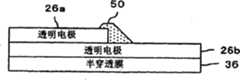
于平坦化膜24上,形成对应像素的显示区的大小的透明电极26,此透明电极26系于接触孔中,连接于驱动TFT14的漏极区域。On the
此透明电极26的周边部分系以第2平坦化膜28所包覆,透明电极26的上方则构成电致发光组件30。The peripheral portion of the
电致发光组件30为有机电致发光组件,于透明电极26与对向电极32之间具备有机化合物(尤其是至少包含有机发光材料的有机层(发光组件层)34)的叠层构造,从阳极注入空穴于有机层34并从阴极注入电子于有机层34,注入于有机层的空穴及电子再次结合,并藉由再结合的能量而激发(excitation)有机发光材料,于返回基底状态之际产生发光。The
在此,透明电极26系由,例如ITO(Indium Tin Oxide,氧化铟锡)及IZO(Indium Zinc Oxide,氧化铟锌)等导电性金属氧化物材料所构成,关于对向电极32则采用具备上部反射膜的功能的铝以及铝合金等。此外,于透明电极26的下层,具备用来在与上部反射膜之间构成微共振器(微空孔)构造的下部反射膜36。Here, the
此例为从透明电极26侧穿透基板10,而将在有机层34所产生的光射出至外部的底放射(bottom emission)型显示装置,下部反射膜36系形成为,具备可让来自于有机层34的光的一部分穿透的半穿透性。一般可采用Ag、Au、Pt、Al中的任一种或这些金属的合金膜来做为此下部反射膜36,并形成为可让光线穿透的程度的薄膜,或是具备网目状或是格子状等开口部的图案。本实施形态并不限定于底放射型显示装置,亦可适用于从组件上方往外部射出光线的所谓的顶放射型显示装置。于适用于顶放射型显示装置的情况下,则并非将下部反射膜36形成为半穿透性,而是使其具备反射性,并将对向电极32形成为具备半穿透性即可。半穿透性的对向电极32系可藉由在例如对向电极的发光组件侧,形成具备Ag、Au等薄膜或细状等开口部的图案的半穿透膜,且在该半穿透膜上叠层ITO等透明电极而实现。This example is a bottom emission (bottom emission) type display device that penetrates the
有机层34系至少具备包含有机发光分子的发光层,并可因应材料,而由单层或是双层、三层、或是四层以上的多层叠层构造所构成。于图1的例中,系藉由真空蒸镀法的连续成膜等,从具备阳极的功能的透明电极26侧开始,依序叠层空穴注入层122、空穴输送层124、发光层126、电子输送层128及电子注入层130,并藉由与有机层34相同的真空蒸镀法,于电子注入层130上,形成具备阴极的功能的对向电极32。此外,电子注入层130亦可视为对向电极32的一部分。The
本实施形态的微空孔构造,系构成于该透明电极26及对向电极32包夹有机层34而互为对向的区域,亦即,透明电极26的下层的下部反射膜36与对向电极32所兼具的上部反射膜之间的层间。在此,此微空孔的光学长度(光学距离)L,系以L=∑nidi...(1)来表示,以形成于下部反射膜36及对向电极32(上部反射膜)的层间的各层的厚度d,与该层的折射率n的乘积和(i为叠层数,为1至i为止的整数)表示。此外,此光学长度L相对于发光波长λ系具备的后述第(3)式所示的关系,藉由设定为具备该关系,可选择性增强波长λ而射出至外部。The microporous structure of this embodiment is formed in the region where the
于全彩的有机电致发光面板当中,一般系具备R、G、B三种色彩的个别像素,并对R、G、B的波长λ(λr、λg、λb),于R、G、B的各像素形成预定的光学长度L(Lr、Lg、Lb)。在此,系采用金属材料来做为下部反射膜36及对向电极32,并于后述的第(3)式中,以φ来表示于此膜产生反射时的相位偏移。In a full-color organic electroluminescent panel, there are generally individual pixels with three colors of R, G, and B, and the wavelength λ (λr, λg, λb) of R, G, and B is different from that of R, G, and B. Each of the pixels forms a predetermined optical length L (Lr, Lg, Lb). Here, a metal material is used for the
于本实施形态中,透明电极26的厚度系于1个像素中有所不同。于图1中,透明电极26的左侧较右侧还厚。因此,左侧部分的光学长度L1较右侧部分的光学长度L2还大(L1>L2),而于1个像素中设定两种的微空孔。In the present embodiment, the thickness of the
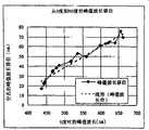
图2显示关于微空孔的空孔长度D,(i)2720(MC=2720),(ii)3800(MC=3800),(iii)无微空孔(参考值),(iv)2720及3800(MC=2720+MC=3800,并使面积比为1∶1的方式而分布)的情况下,各自发出绿色光的有机电致发光组件的视角依存性。图2显示CIE显色系的色度图(Yxy)。在此,所谓的空孔长度D,是指为了共振预定波长的光而要求的用来达成上述光学长度L的反射膜及半穿透膜之间的实际膜厚(膜厚合计),系以D=∑di...(2)来表示。Fig. 2 shows about the void length D of microvoid, (i) 2720 (MC=2720), (ii) 3800 (MC=3800), (iii) without microvoid (reference value), (iv) 2720 and 3800 (MC=2720+MC=3800, and distributed so that the area ratio is 1:1), the viewing angle dependence of the organic electroluminescent elements that emit green light. Figure 2 shows the chromaticity diagram (Yxy) of the CIE color system. Here, the so-called pore length D refers to the actual film thickness (total film thickness) between the reflective film and the semi-transmissive film required to achieve the above-mentioned optical length L in order to resonate light of a predetermined wavelength. D=∑di...(2) to represent.
MC=2720系如图中的×所示,于视角为00中,具备570nm的共振波长,为右下(x=0.39,y=0.58)所表示的色度,随着视角的增大,共振波长会往短波长侧移位(往图中的左上方向移动)。于视角为600中,具备520nm的共振波长,可获得色纯度极高的绿色,而处于图中的左上方(x=0.21,y=0.71)。MC=2720 is shown by the × in the figure. When the viewing angle is 00, it has a resonance wavelength of 570nm, which is the chromaticity represented by the lower right (x=0.39, y=0.58). As the viewing angle increases, the resonance The wavelength shifts to the shorter wavelength side (moves to the upper left in the figure). At a viewing angle of 600, with a resonance wavelength of 520nm, green with extremely high color purity can be obtained, and it is located in the upper left of the figure (x=0.21, y=0.71).
另一方面,MC=3800显示黑色三角,于视角为00中,具备510nm的共振波长,于图中的左上方(x=0.19,y=0.69)虽然具备色纯度极高的绿色,但随着视角的增大,共振波长往短波长侧移位,而往图中的右上方移动,于视角为600中,处于右上方(x=0.37,y=0.55)的位置。依据此组件所采用的有机发光材料的发光频谱(spectrum),于绿色具备峰值,且不具蓝色成分,因此,随着视角的增大,即使共振波长移位,于原先的发光频谱中该共振波长较小,因此组件的发光强度会降低,而使绿色成为半穿透光。参考值系以◇显示,该移动范围约为x=0.30至0.33,y=0.60至0.63左右,视角依存性相对较小。于本实施形态的MC=2720+MC=3800中,该视角依存性系较设定空孔条件为1种时还小。亦即,于视角为00中,可藉由MC=3800,于视角为600中,可藉由MC=2720来表现出极高的色纯度,因此不论于何种视角,均可维持极高的色纯度。因此,于组合复数空孔长度互为不同的区域的组件中,色度的移动范围约为x=0.27至0.29,y=0.63至0.65左右,于色度图上位于较参考值更左上方的位置,且色移位较小,因此可提升色纯度。On the other hand, MC=3800 shows a black triangle, and has a resonance wavelength of 510nm in the viewing angle of 00. Although the upper left of the figure (x=0.19, y=0.69) has a green color with extremely high color purity, but with As the viewing angle increases, the resonance wavelength shifts to the short-wavelength side and moves to the upper right in the figure. When the viewing angle is 600, it is at the upper right (x=0.37, y=0.55). According to the emission spectrum (spectrum) of the organic light-emitting material used in this component, it has a peak in green and has no blue component. Therefore, as the viewing angle increases, even if the resonance wavelength shifts, the resonance in the original emission spectrum The wavelength is smaller, so the luminous intensity of the component will be reduced, making the green a semi-transparent light. The reference value is shown by ◇, the moving range is about x=0.30 to 0.33, y=0.60 to 0.63, and the viewing angle dependence is relatively small. In the case of MC=2720+MC=3800 in the present embodiment, the viewing angle dependence is smaller than when one hole condition is set. That is to say, when the viewing angle is 00, MC=3800 can be used, and when the viewing angle is 600, MC=2720 can be used to express extremely high color purity, so no matter what viewing angle, it can maintain a very high color purity. color purity. Therefore, in a component that combines multiple areas with different pore lengths, the shift range of chromaticity is about x=0.27 to 0.29, and y=0.63 to 0.65, which is located on the upper left of the reference value on the chromaticity diagram. Position, and the color shift is small, so the color purity can be improved.
如此,根据本实施形态的构成,于1个像素内各自构成2720及3800左右的2种厚度(约1100左右的段差)的微空孔,而可于绿色光中大幅改善(降低)视角依存性。In this way, according to the configuration of this embodiment, microvoids with two types of thicknesses of about 2720 and 3800 (step difference of about 1100) are respectively formed in one pixel, and the viewing angle dependence can be greatly improved (reduced) in green light .
在此,共振条件及共振波长的角度依存性,系以下式(3)来表示。Here, the angle dependence of the resonance condition and the resonance wavelength is represented by the following equation (3).
[数学式1][mathematical formula 1]
2Lcosθ’/λ’+ψ/2π=m(m:整数)...(3)2Lcosθ'/λ'+ψ/2π=m(m: integer)...(3)
θ’=sin-1{(sinθ)/n};λ’=λ+(cosθ-1)λθ'=sin-1{(sinθ)/n}; λ'=λ+(cosθ-1)λ
式中的L为上述的光学长度L(=∑nidi),ψ为表示金属的反射所造成的相位偏移的常数,θ为角度(视角)。In the formula, L is the above-mentioned optical length L (=Σnidi), ψ is a constant indicating a phase shift due to reflection of metal, and θ is an angle (viewing angle).
图3显示横轴为视角为00的峰值波长,纵轴为视角为600时的峰值波长往短波长侧的移位量。空孔长度D设定为4500至5500。如此,于视角为00的峰值波长约为450nm左右中,视角为600时的波长的移位量约为28nm左右。于视角为00时的峰值波长约为600nm左右的条件中,视角为600时的波长的移位量约为60nm左右。Figure 3 shows that the horizontal axis is the peak wavelength at a viewing angle of 00, and the vertical axis is the shift amount of the peak wavelength to the short wavelength side when the viewing angle is 600. The hole length D is set at 4500 to 5500. In this way, when the viewing angle is 00 and the peak wavelength is about 450 nm, the wavelength shift amount when the viewing angle is 600 is about 28 nm. Under the condition that the peak wavelength is about 600 nm when the viewing angle is 00, the shift amount of the wavelength when the viewing angle is 600 is about 60 nm.
如此,于视角为00时于600nm具备峰值的波形,系于600的视角方向中往60nm的短方向移位,而成为于540nm具备峰值的波形。因此,于绿色550nm中为了进行内插(interpolation),系组合大约600nm至700nm左右的空孔长度D(用来共振600nm至700nm的波长的空孔长度D)。关于段差,在上述式中m=1时,大约为1000(100nm)至1300(nm)。Thus, the waveform having a peak at 600 nm when the viewing angle is 00 is shifted in the short direction of 60 nm in the viewing angle direction of 600 to become a waveform having a peak at 540 nm. Therefore, for interpolation in green 550 nm, a pore length D of approximately 600 nm to 700 nm (a pore length D for resonance at a wavelength of 600 nm to 700 nm) is combined. Regarding the step difference, when m=1 in the above formula, it is about 1000 (100 nm) to 1300 (nm).
MC=2720及MC=3800相对于00的光的共振波长各为570nm(m=1)及510nm(m=2)。亦即,于上述例中,由于视角依存性较小且对绿色设定微空孔,因此于视角为00之际,系于1个像素内,组合以510nm及570nm为共振波长的空孔长度D而形成。The resonance wavelengths of MC=2720 and MC=3800 with respect to light of 00 are 570 nm (m=1) and 510 nm (m=2), respectively. That is, in the above example, since the viewing angle dependence is small and the micropores are set for green, when the viewing angle is 00, the lengths of the pores whose resonance wavelengths are 510nm and 570nm are combined in one pixel D is formed.
此外,于红色的630nm中,较理想为组合大约700nm至800nm左右的空孔长度D,段差系在上述式中m=0时,大致为1600左右。此外,于蓝色的4500nm中,较理想为组合大约480nm至580nm左右的空孔长度D,段差系于m=1之际,大致为1000左右。In addition, in the red 630nm, it is ideal to combine the pore length D of about 700nm to 800nm, and the step difference is about 1600 when m=0 in the above formula. In addition, in the blue 4500nm, it is ideal to combine the pore length D of about 480nm to 580nm, and the step difference is about 1000 when m=1.
段差的值乃因m的选择而有所不同,就考虑到段差覆盖性,则段差较理想为2000以下。亦即,于定义1个像素中的空孔长度互为不同的区域为第1区域(例如上述MC3800)及第2区域(例如上述MC2720)时,第1区域的空孔长度D及第2区域的空孔长度D较理想为,各自考量到目的的共振波长、原先的发光频谱、与彩色滤光片的组合时的滤光特性等,而各自决定,但空孔长度的差(段差)较理想为200nm(2000)以内。藉由设定于此范围,即使例如如上所述的变更透明电极的厚度而形成第1区域及第2区域时,亦可藉由形成于透明电极的段差,而防止电极的上层的断线等。例如,考量到电子输送层的厚度若愈厚则驱动电压上升等,此电压上升并不理想,因此较多为设定在未满3000的厚度,而从防止电子输送层因为此段差而造成断线的观点来看,段差较理想为200nm以下。The value of the step difference is different due to the choice of m. Considering the step difference coverage, the step difference is ideally below 2000. In other words, when defining regions with different hole lengths in one pixel as the first region (such as the MC3800 mentioned above) and the second region (such as the MC2720 mentioned above), the hole length D of the first region and the hole length D of the second region The pore length D is ideally determined by considering the resonant wavelength of the purpose, the original emission spectrum, and the filter characteristics when combined with color filters, etc., but the difference in pore length (step difference) is relatively small. Ideally within 200nm (2000). By setting within this range, for example, even when the first region and the second region are formed by changing the thickness of the transparent electrode as described above, the level difference formed in the transparent electrode can prevent disconnection of the upper layer of the electrode, etc. . For example, considering that the driving voltage increases when the thickness of the electron transport layer is thicker, etc., this voltage increase is not ideal, so it is often set at a thickness less than 3000 to prevent the electron transport layer from being broken due to this step difference. From the viewpoint of the line, the step difference is ideally 200nm or less.
如上所述,于获得某色彩的1个像素区域中,藉由设定复数空孔长度D,可改善视角依存性而提升色纯度,在此,系将所选择的复数空孔长度D例如设定为:于第1区域的1个空孔长度D形成为于视角为00时的原先目的的共振波长成为峰值波长的厚度,第2区域的与第1区域不同的空孔长度D系形成为于其它视角(例如600)时的目的的共振波长成为峰值波长的厚度。于以上的说明中,系于1个像素形成2种空孔长度D互为不同的区域,但是并不限定于2种,并可依所需而设定为3种以上。As mentioned above, in one pixel region where a certain color is obtained, by setting the length D of multiple holes, the viewing angle dependence can be improved and the color purity can be improved. Here, the selected length D of multiple holes is set as The length D of one pore in the first region is formed so that the original intended resonance wavelength becomes the peak wavelength when the viewing angle is 00, and the pore length D in the second region is formed as follows: The target resonance wavelength at other viewing angles (for example, 600) becomes the thickness of the peak wavelength. In the above description, two types of regions having different hole lengths D are formed in one pixel, but the region is not limited to two types, and may be set to three or more types as necessary.
上述的实施形态中系利用以各像素的发光波长为RGB中任一者的方式来个别设定发光层材料的RGB分开涂布的型式。除此之外,亦有发光层本身可发出白色光,并藉由彩色滤光片来设定发光色的型式。于此情况下,亦可藉由微空孔的共振波长的选择,而增强各种色彩的光线。而白色发光的发光层系可形成为各像素共通层。In the above-mentioned embodiment, the RGB separate coating type which individually sets the light emitting layer material so that the light emission wavelength of each pixel may be any of RGB is utilized. In addition, there is also a type in which the luminescent layer itself can emit white light, and the luminescent color is set by a color filter. In this case, the light of various colors can also be enhanced by selecting the resonant wavelength of the micro-holes. The white light-emitting layer can be formed as a common layer for each pixel.
图4显示于设定为白色+彩色滤光片(绿)的像素构造,且设定微空孔的空孔长度D为CL1=2600(目的共振波长560nm)及CL2=3000(辅助共振波长600nm)的2种(段差400)的情况下,变更各个空孔长度D的部份的面积比时的色度变化。在此m=2。在此,Δu’、Δv’为CIELUV显色系的u’、v’的变化量,横轴为视角,纵轴为色彩变化量(Δu’及Δv’的平方和√(Δu’2+Δv’2))。Figure 4 shows the pixel structure set to white + color filter (green), and the hole length D of the microhole is set as CL1=2600 (the target resonance wavelength is 560nm) and CL2=3000 (the auxiliary resonance wavelength is 600nm) ) in the case of two types (step difference 400), the change in chromaticity when the area ratio of the portion of each pore length D is changed. Here m=2. Here, Δu' and Δv' are the changes of u' and v' of the CIELUV color system, the horizontal axis is the viewing angle, and the vertical axis is the color change (the square sum of Δu' and Δv'√(Δu'2+Δv '2)).
从该结果中可得知,在CL1/CL2的面积比为80/20至60/40的范围内,色彩变化量最少且特性优异。可对应发光频谱而变更最适当的面积比。若与白色组件组合的彩色滤光片的色彩不同,则可对应该色彩(包含彩色滤光片的特性)而设定最适当的面积比。此外,较理想为对应所采用的有机电致发光材料,亦即对应白色光的频谱而设定最适当的面积比。当然,亦可因目的的共振波长的不同而进行最适化。From this result, it can be seen that within the range of the area ratio of CL1/CL2 of 80/20 to 60/40, the amount of color change is the least and the characteristics are excellent. The optimum area ratio can be changed according to the emission spectrum. If the color of the color filter combined with the white element is different, an optimum area ratio can be set according to the color (including the characteristics of the color filter). In addition, it is desirable to set the most appropriate area ratio corresponding to the organic electroluminescent material used, that is, corresponding to the spectrum of white light. Of course, optimization may be performed depending on the desired resonance wavelength.
图5显示关于图4的各个面积比的色彩变化量,于获得辅助共振波长600nm的CL2的1个像素内的比例与色彩变化量的关系。在此,√(Δu’2+Δv’2)的值较理想为0.08以下。从图5中可得知,CL2的面积较理想为设定在10%至60%的范围。亦即,于将1个像素中的空孔长度D互为不同的区域设定为第1区域(例如CL1)及第2区域(例如CL2)的情况下,最好将该辅助共振波长较第1区域的目的共振波长还长的第2区域的于1个像素内的面积设定为10%至60%的范围。FIG. 5 shows the relationship between the color change amount and the ratio within one pixel of CL2 at which an auxiliary resonance wavelength of 600 nm is obtained, and the color change amount for each area ratio of FIG. 4 . Here, the value of √(Δu'2+Δv'2) is preferably 0.08 or less. It can be known from FIG. 5 that the area of CL2 is ideally set in the range of 10% to 60%. That is, when the regions in which the pore lengths D in one pixel are different from each other are set as the first region (for example, CL1) and the second region (for example, CL2), it is preferable to set the auxiliary resonance wavelength to be higher than that of the second region. The area within one pixel of the second region where the target resonance wavelength of the first region is longer is set to a range of 10% to 60%.
再者,由图4可得知,在视角比60度更小时,例如在小于55度左右的条件下,即使在第2区域CL2的1像素内的面积为比20%更小的值,只要比0%大,则√(Δu’2+Δv’2)的值为0.08以下,可抑制颜色变化。因此,即使在例如第2区域的1像素内的面积为1%至60%的范围,亦可实际有效地实现颜色变化较小的组件。Furthermore, as can be seen from FIG. 4, when the viewing angle is smaller than 60 degrees, for example, under the condition of less than about 55 degrees, even if the area within one pixel in the second region CL2 is a value smaller than 20%, as long as When it is larger than 0%, the value of √(Δu'2+Δv'2) is 0.08 or less, and the color change can be suppressed. Therefore, even if the area within one pixel of the second region is, for example, in the range of 1% to 60%, it is actually possible to effectively realize a device with a small color change.
在此,于本实施形态中,为了变更微空孔的长度,系藉由变更透明电极26的厚度来对应。因此,可于透明电极26的形成步骤中进行2阶段的叠层。亦即,只要进行于较薄的部分(例如第1区域)及较厚的部分(例如第2区域)的双方的部分叠层电极材料的步骤,及仅于较厚的部分叠层电极材料的步骤即可,任一项步骤均可先进行。Here, in the present embodiment, in order to change the length of the micropores, the thickness of the
例如,如图6所示,分2次叠层透明电极26,第1次在整体叠层(例如真空蒸镀及溅镀)透明电极26a,第2次仅在较厚的部分叠层透明电极26b。于此情况下,如图7所示,较理想为将较厚的部分(叠层透明电极26b的部分)分割为多数区域而形成为岛状。如此,由于较厚的部分系呈点状而分散存在,因此可进行像素全体的比较一致性的显示。此外,在此相对于在视角为00中达成目的共振波长的第1区域,达成辅助共振波长(较目的共振波长更长的波长侧)的第2区域,不仅于1个像素内呈点状而分散存在,并且将所分割的各区域的面积设为1个像素面积的1/4(25%)以下。若设定为25%以下,则即使共振波长互为不同的区域存在于1个像素内,亦可防止难以辨识,并防止显示品质的降低。For example, as shown in FIG. 6, the
此外,如图8所示,较理想为形成用来包覆由透明电极26a、26b所形成的段差部分的绝缘层50。藉由设置此绝缘层50,可使此段差部分平坦化,而防止形成于上方的各层的断裂及阴极的断线等的产生。Moreover, as shown in FIG. 8, it is desirable to form the insulating
此外,如图9所示,较理想为,亦于设定较长的空孔长度D的区域的半穿透膜36与透明电极26之间,配置透明的绝缘层(例如SiN)52。借此,可增大空孔长度D仅绝缘层52的量。于此情况下,若采用低倾斜(taper)材料来做为绝缘层52,则可防止断线。In addition, as shown in FIG. 9 , it is preferable to arrange a transparent insulating layer (for example, SiN) 52 between the
如上所述,根据本实施形态,乃变更1个像素区域内的微空孔的空孔长度D。因此,于视角改变的情况下,所增强的光的波长会因场所的不同而不同,而可补偿于单一空孔长度D时的色彩的移位,而减少色彩的视角依存性。As described above, according to the present embodiment, the pore length D of the micropores in one pixel region is changed. Therefore, when the viewing angle changes, the wavelength of the enhanced light will vary from place to place, which can compensate for the color shift at a single hole length D, thereby reducing the viewing angle dependence of the color.
此外,于以上的说明中,为了变更1个像素区域内的空孔长度D,而改变透明电极26厚度,但是并不限定于此,例如可于1个像素区域内,变更图1所示的发光组件层34的厚度,而改变空孔长度D。In addition, in the above description, the thickness of the
于1个像素区域内设置空孔长度互为不同的复数区域时,区域的比例(面积比)可设定为,即使分配至像素的发光波长(亦即射入于微空孔的光)不同,亦可于所有像素为共通。然而,由于共振条件会因有机电致发光组件的原始发光波长的不同而不同,因此更理想为,对于每种色彩亦即每个色彩不同的像素最适化该面积比,而达到不论任何色彩均能够降低视角依存性的适当比例。因此,于存在R、G、B三种色彩的像素时,于R、G、B的至少一种色彩的像素与其它色彩的像素,第1区域及第2区域的面积比互为不同。于存在R、G、B、W四种色彩的像素时,至少改变4色当中的1种色彩像素与另1种色彩像素的面积比。如此,对每种色彩改变面积比者,即使于例如R、G、B的各像素分开涂布发光材料而进行彩色显示的显示装置中,或是于所有像素采用白色发光组件并藉由彩色滤光片来进行彩色显示的显示装置中,皆极为理想。此外,不限于面积比,由于第1区域及第2区域的各个空孔长度D,系因色彩的不同,及共振模式(m的值)的不同,及原先的发光频谱波形等的不同等而有所不同,因此较理想为依据所采用的条件而调整空孔长度D。When a plurality of regions with different hole lengths are provided in one pixel region, the ratio (area ratio) of the regions can be set so that even if the wavelength of light emitted to the pixel (that is, the light incident on the micropore) is different , can also be common to all pixels. However, since the resonance conditions differ depending on the original emission wavelength of the organic electroluminescent element, it is more desirable to optimize the area ratio for each color, that is, for each pixel with a different color, so as to achieve Both can reduce the appropriate ratio of viewing angle dependence. Therefore, when there are pixels of three colors of R, G, and B, the area ratios of the first region and the second region are different between pixels of at least one color of R, G, and B and pixels of other colors. When there are pixels of four colors of R, G, B, and W, at least the area ratio of one color pixel to another color pixel among the four colors is changed. In this way, if the area ratio is changed for each color, even in a display device such as R, G, and B, each pixel is separately coated with a light-emitting material to perform color display, or a white light-emitting component is used for all pixels and is passed through a color filter. It is ideal in a display device that performs color display using a light sheet. In addition, it is not limited to the area ratio, because the length D of each hole in the first region and the second region is different due to the difference in color, the difference in the resonance mode (the value of m), and the difference in the original emission spectrum waveform. are different, so it is ideal to adjust the pore length D according to the conditions used.
此外,换言之,于第1区域及第2区域视角为00(正面)中,获得目的共振波长的第1区域及获得辅助共振波长的第2区域(于其它的视角下实现目的共振波长的区域)的面积比,不仅可对应发光色等而变更,亦可对应显示面板上的像素位置而变更。例如于面板的中央位置,以视角为00所观察的位置系一般的观察位置时,相对于面板的周围区域的一般的视角并不为00。因此,更理想为对应面板位置,亦即考量到距离一般观察位置的视角的不同,而变更各像素的第1区域及第2区域的面积比例。关于相同颜色像素的第1区域及第2区域的各个空孔长度D,亦可对应面板的位置而进行调整。于面板达到大型化的情况下,由于面板的中央位置及周围位置的视角差极大,因此,对应位置而进行变更者系于显示装置的大画面化时极为有效。In addition, in other words, in the first region and the second region where the viewing angle is 00 (front), the first region where the target resonance wavelength is obtained and the second region where the auxiliary resonance wavelength is obtained (the region where the target resonance wavelength is achieved at other viewing angles) The area ratio can be changed not only according to the luminous color, etc., but also according to the pixel position on the display panel. For example, at the central position of the panel, when the position observed with the viewing angle of 00 is a general viewing position, the general viewing angle relative to the surrounding area of the panel is not 00. Therefore, it is more desirable to change the area ratio of the first region and the second region of each pixel in accordance with the position of the panel, that is, in consideration of the difference in viewing angle from the general observation position. The hole lengths D of the first region and the second region of the pixels of the same color can also be adjusted according to the position of the panel. When the size of the panel is increased, since the viewing angle difference between the central position and the peripheral position of the panel is extremely large, it is very effective to change the corresponding position when the screen of the display device is increased.
于本实施形态中,于每个像素分开涂布R、G、B的发光材料时,如上所述,系于各像素设置空孔长度互为不同的复数区域,除了此构成之外,亦可于各像素上分别设置彩色滤光片。在此,如图10所示,彩色滤光片60可设置于例如层间绝缘膜20与平坦化膜24之间,或是设置于平坦化膜24与半穿透膜36之间。In this embodiment, when each pixel is separately coated with R, G, and B light-emitting materials, as described above, a plurality of regions with different hole lengths are provided in each pixel. In addition to this configuration, it is also possible to A color filter is respectively arranged on each pixel. Here, as shown in FIG. 10 , the
于分开涂布时,本质上不需要彩色滤光片,但是由于在1个像素内存在空孔长度互为不同的区域,而于例如视角为00的情况下,即使于第1区域中获得最适当的共振波长,亦增强于第2区域中不见得为最适当的波长,并加以射出。因此,若以上述的绿色的有机电致发光组件为例,则可对此组件形成复数空孔,并设置绿色的彩色滤光片,并使其仅穿透所期望的波长区,借此,不论视角为何,均可获得色纯度更高的绿色光线。此外,于此情况下,如图11所示彩色滤光片60可形成于1个像素区域内的全部,亦可仅形成于对应空孔长度不同的任一区域(于上述中为第2区域)的区域。In the case of separate coating, a color filter is essentially unnecessary, but since there are areas with different pore lengths in one pixel, for example, when the viewing angle is 00, the best color filter can be obtained even in the first area. Appropriate resonance wavelengths are also amplified and emitted that are not necessarily the most appropriate wavelengths in the second region. Therefore, if the above-mentioned green organic electroluminescent component is taken as an example, a plurality of holes can be formed on this component, and a green color filter can be provided to only penetrate the desired wavelength region, thereby, Green light with higher color purity is obtained regardless of the viewing angle. In addition, in this case, as shown in FIG. 11 , the
Claims (14)
Applications Claiming Priority (2)
| Application Number | Priority Date | Filing Date | Title |
|---|---|---|---|
| JP2004181850 | 2004-06-18 | ||
| JP2004181850 | 2004-06-18 |
Publications (2)
| Publication Number | Publication Date |
|---|---|
| CN1717135A CN1717135A (en) | 2006-01-04 |
| CN100459213Ctrue CN100459213C (en) | 2009-02-04 |
Family
ID=35479927
Family Applications (1)
| Application Number | Title | Priority Date | Filing Date |
|---|---|---|---|
| CNB2005100773142AExpired - LifetimeCN100459213C (en) | 2004-06-18 | 2005-06-20 | Electroluminescence panel |
Country Status (4)
| Country | Link |
|---|---|
| US (1) | US7548019B2 (en) |
| KR (1) | KR20060046476A (en) |
| CN (1) | CN100459213C (en) |
| TW (1) | TWI272039B (en) |
Families Citing this family (98)
| Publication number | Priority date | Publication date | Assignee | Title |
|---|---|---|---|---|
| US8339037B2 (en)* | 2004-03-26 | 2012-12-25 | Panasonic Corporation | Organic light emitting device with reduced angle dependency |
| US8188315B2 (en) | 2004-04-02 | 2012-05-29 | Samsung Mobile Display Co., Ltd. | Organic light emitting device and flat panel display device comprising the same |
| JP4573672B2 (en)* | 2005-02-28 | 2010-11-04 | 三洋電機株式会社 | Organic EL panel |
| JP4411288B2 (en)* | 2005-03-23 | 2010-02-10 | キヤノン株式会社 | Display device |
| JP4645587B2 (en)* | 2006-02-03 | 2011-03-09 | ソニー株式会社 | Display element and display device |
| TWI363441B (en)* | 2007-02-09 | 2012-05-01 | Au Optronics Corp | Self-emissive display device |
| CN101017884B (en)* | 2007-02-28 | 2013-08-14 | 友达光电股份有限公司 | Self-lighting display device |
| JP4479737B2 (en)* | 2007-03-07 | 2010-06-09 | セイコーエプソン株式会社 | LIGHT EMITTING DEVICE, ITS MANUFACTURING METHOD, AND ELECTRONIC DEVICE |
| CN101051676B (en)* | 2007-05-15 | 2010-10-06 | 友达光电股份有限公司 | Organic electroluminescent pixel, organic electroluminescent element and manufacturing method thereof |
| US7855508B2 (en)* | 2007-09-17 | 2010-12-21 | Global Oled Technology Llc | LED device having improved light output |
| US8076838B2 (en)* | 2007-10-31 | 2011-12-13 | Seiko Epson Corporation | Light emitting device |
| KR101458905B1 (en) | 2008-02-12 | 2014-11-07 | 삼성디스플레이 주식회사 | Organic light emitting display and manufacturing method thereof |
| US7825581B2 (en) | 2008-02-12 | 2010-11-02 | Samsung Electronics Co., Ltd. | Organic light emitting diode display and method for manufacturing the same |
| JP2009231274A (en)* | 2008-02-27 | 2009-10-08 | Canon Inc | Organic light-emitting element, and display apparatus |
| KR101469031B1 (en)* | 2008-04-16 | 2014-12-05 | 삼성디스플레이 주식회사 | Organic light emitting display |
| KR101448004B1 (en)* | 2008-04-22 | 2014-10-07 | 삼성디스플레이 주식회사 | Organic light emitting display |
| JP5251239B2 (en)* | 2008-05-08 | 2013-07-31 | セイコーエプソン株式会社 | ORGANIC EL DEVICE, ELECTRONIC DEVICE, ORGANIC EL DEVICE MANUFACTURING METHOD |
| KR101592013B1 (en)* | 2008-10-13 | 2016-02-05 | 삼성디스플레이 주식회사 | Organic light emitting diode display and method for manufacturing the same |
| US8433446B2 (en) | 2008-10-27 | 2013-04-30 | Lennox Industries, Inc. | Alarm and diagnostics system and method for a distributed-architecture heating, ventilation and air conditioning network |
| US8892797B2 (en) | 2008-10-27 | 2014-11-18 | Lennox Industries Inc. | Communication protocol system and method for a distributed-architecture heating, ventilation and air conditioning network |
| US8295981B2 (en) | 2008-10-27 | 2012-10-23 | Lennox Industries Inc. | Device commissioning in a heating, ventilation and air conditioning network |
| US8655490B2 (en) | 2008-10-27 | 2014-02-18 | Lennox Industries, Inc. | System and method of use for a user interface dashboard of a heating, ventilation and air conditioning network |
| US8615326B2 (en) | 2008-10-27 | 2013-12-24 | Lennox Industries Inc. | System and method of use for a user interface dashboard of a heating, ventilation and air conditioning network |
| US8442693B2 (en) | 2008-10-27 | 2013-05-14 | Lennox Industries, Inc. | System and method of use for a user interface dashboard of a heating, ventilation and air conditioning network |
| US8661165B2 (en) | 2008-10-27 | 2014-02-25 | Lennox Industries, Inc. | Device abstraction system and method for a distributed architecture heating, ventilation and air conditioning system |
| US8548630B2 (en) | 2008-10-27 | 2013-10-01 | Lennox Industries, Inc. | Alarm and diagnostics system and method for a distributed-architecture heating, ventilation and air conditioning network |
| US8463442B2 (en) | 2008-10-27 | 2013-06-11 | Lennox Industries, Inc. | Alarm and diagnostics system and method for a distributed architecture heating, ventilation and air conditioning network |
| US9152155B2 (en) | 2008-10-27 | 2015-10-06 | Lennox Industries Inc. | Device abstraction system and method for a distributed-architecture heating, ventilation and air conditioning system |
| US8560125B2 (en) | 2008-10-27 | 2013-10-15 | Lennox Industries | Communication protocol system and method for a distributed-architecture heating, ventilation and air conditioning network |
| US8725298B2 (en) | 2008-10-27 | 2014-05-13 | Lennox Industries, Inc. | Alarm and diagnostics system and method for a distributed architecture heating, ventilation and conditioning network |
| US8352081B2 (en) | 2008-10-27 | 2013-01-08 | Lennox Industries Inc. | Communication protocol system and method for a distributed-architecture heating, ventilation and air conditioning network |
| US9325517B2 (en) | 2008-10-27 | 2016-04-26 | Lennox Industries Inc. | Device abstraction system and method for a distributed-architecture heating, ventilation and air conditioning system |
| US8255086B2 (en) | 2008-10-27 | 2012-08-28 | Lennox Industries Inc. | System recovery in a heating, ventilation and air conditioning network |
| US8437878B2 (en) | 2008-10-27 | 2013-05-07 | Lennox Industries Inc. | Alarm and diagnostics system and method for a distributed architecture heating, ventilation and air conditioning network |
| US9678486B2 (en) | 2008-10-27 | 2017-06-13 | Lennox Industries Inc. | Device abstraction system and method for a distributed-architecture heating, ventilation and air conditioning system |
| US9261888B2 (en) | 2008-10-27 | 2016-02-16 | Lennox Industries Inc. | System and method of use for a user interface dashboard of a heating, ventilation and air conditioning network |
| US8564400B2 (en) | 2008-10-27 | 2013-10-22 | Lennox Industries, Inc. | Communication protocol system and method for a distributed-architecture heating, ventilation and air conditioning network |
| US9268345B2 (en) | 2008-10-27 | 2016-02-23 | Lennox Industries Inc. | System and method of use for a user interface dashboard of a heating, ventilation and air conditioning network |
| US8600559B2 (en) | 2008-10-27 | 2013-12-03 | Lennox Industries Inc. | Method of controlling equipment in a heating, ventilation and air conditioning network |
| US8744629B2 (en) | 2008-10-27 | 2014-06-03 | Lennox Industries Inc. | System and method of use for a user interface dashboard of a heating, ventilation and air conditioning network |
| US8452456B2 (en) | 2008-10-27 | 2013-05-28 | Lennox Industries Inc. | System and method of use for a user interface dashboard of a heating, ventilation and air conditioning network |
| US9377768B2 (en) | 2008-10-27 | 2016-06-28 | Lennox Industries Inc. | Memory recovery scheme and data structure in a heating, ventilation and air conditioning network |
| US8802981B2 (en) | 2008-10-27 | 2014-08-12 | Lennox Industries Inc. | Flush wall mount thermostat and in-set mounting plate for a heating, ventilation and air conditioning system |
| US8788100B2 (en) | 2008-10-27 | 2014-07-22 | Lennox Industries Inc. | System and method for zoning a distributed-architecture heating, ventilation and air conditioning network |
| US8463443B2 (en) | 2008-10-27 | 2013-06-11 | Lennox Industries, Inc. | Memory recovery scheme and data structure in a heating, ventilation and air conditioning network |
| US8437877B2 (en) | 2008-10-27 | 2013-05-07 | Lennox Industries Inc. | System recovery in a heating, ventilation and air conditioning network |
| US8874815B2 (en) | 2008-10-27 | 2014-10-28 | Lennox Industries, Inc. | Communication protocol system and method for a distributed architecture heating, ventilation and air conditioning network |
| US8855825B2 (en) | 2008-10-27 | 2014-10-07 | Lennox Industries Inc. | Device abstraction system and method for a distributed-architecture heating, ventilation and air conditioning system |
| US8762666B2 (en) | 2008-10-27 | 2014-06-24 | Lennox Industries, Inc. | Backup and restoration of operation control data in a heating, ventilation and air conditioning network |
| US8600558B2 (en) | 2008-10-27 | 2013-12-03 | Lennox Industries Inc. | System recovery in a heating, ventilation and air conditioning network |
| US8655491B2 (en) | 2008-10-27 | 2014-02-18 | Lennox Industries Inc. | Alarm and diagnostics system and method for a distributed architecture heating, ventilation and air conditioning network |
| US9632490B2 (en) | 2008-10-27 | 2017-04-25 | Lennox Industries Inc. | System and method for zoning a distributed architecture heating, ventilation and air conditioning network |
| US8543243B2 (en) | 2008-10-27 | 2013-09-24 | Lennox Industries, Inc. | System and method of use for a user interface dashboard of a heating, ventilation and air conditioning network |
| US8798796B2 (en) | 2008-10-27 | 2014-08-05 | Lennox Industries Inc. | General control techniques in a heating, ventilation and air conditioning network |
| US8774210B2 (en) | 2008-10-27 | 2014-07-08 | Lennox Industries, Inc. | Communication protocol system and method for a distributed-architecture heating, ventilation and air conditioning network |
| US8239066B2 (en) | 2008-10-27 | 2012-08-07 | Lennox Industries Inc. | System and method of use for a user interface dashboard of a heating, ventilation and air conditioning network |
| US8977794B2 (en) | 2008-10-27 | 2015-03-10 | Lennox Industries, Inc. | Communication protocol system and method for a distributed-architecture heating, ventilation and air conditioning network |
| US8994539B2 (en) | 2008-10-27 | 2015-03-31 | Lennox Industries, Inc. | Alarm and diagnostics system and method for a distributed-architecture heating, ventilation and air conditioning network |
| US8352080B2 (en) | 2008-10-27 | 2013-01-08 | Lennox Industries Inc. | Communication protocol system and method for a distributed-architecture heating, ventilation and air conditioning network |
| US8694164B2 (en) | 2008-10-27 | 2014-04-08 | Lennox Industries, Inc. | Interactive user guidance interface for a heating, ventilation and air conditioning system |
| US9432208B2 (en) | 2008-10-27 | 2016-08-30 | Lennox Industries Inc. | Device abstraction system and method for a distributed architecture heating, ventilation and air conditioning system |
| US9651925B2 (en) | 2008-10-27 | 2017-05-16 | Lennox Industries Inc. | System and method for zoning a distributed-architecture heating, ventilation and air conditioning network |
| US8452906B2 (en) | 2008-10-27 | 2013-05-28 | Lennox Industries, Inc. | Communication protocol system and method for a distributed-architecture heating, ventilation and air conditioning network |
| KR101582938B1 (en)* | 2008-11-20 | 2016-01-08 | 삼성디스플레이 주식회사 | Organic light emitting display |
| KR101582941B1 (en) | 2008-12-24 | 2016-01-08 | 삼성디스플레이 주식회사 | Organic light emitting device and manufacturing method thereof |
| USD648642S1 (en) | 2009-10-21 | 2011-11-15 | Lennox Industries Inc. | Thin cover plate for an electronic system controller |
| USD648641S1 (en) | 2009-10-21 | 2011-11-15 | Lennox Industries Inc. | Thin cover plate for an electronic system controller |
| US8260444B2 (en) | 2010-02-17 | 2012-09-04 | Lennox Industries Inc. | Auxiliary controller of a HVAC system |
| JP2012003925A (en) | 2010-06-16 | 2012-01-05 | Sony Corp | Display device |
| KR20120042066A (en)* | 2010-10-22 | 2012-05-03 | 삼성모바일디스플레이주식회사 | Organic light emitting diode display |
| KR101894898B1 (en) | 2011-02-11 | 2018-09-04 | 가부시키가이샤 한도오따이 에네루기 켄큐쇼 | Light-emitting device and electronic device using light-emitting device |
| JP5969216B2 (en) | 2011-02-11 | 2016-08-17 | 株式会社半導体エネルギー研究所 | Light emitting element, display device, lighting device, and manufacturing method thereof |
| KR101960759B1 (en) | 2011-04-08 | 2019-03-21 | 가부시키가이샤 한도오따이 에네루기 켄큐쇼 | Light-emitting device, electronic appliance, and lighting device |
| KR101917752B1 (en) | 2011-05-11 | 2018-11-13 | 가부시키가이샤 한도오따이 에네루기 켄큐쇼 | Light-emitting element, light-emitting module, light-emmiting panel, and light-emitting device |
| WO2013008765A1 (en) | 2011-07-08 | 2013-01-17 | Semiconductor Energy Laboratory Co., Ltd. | Light-emitting module, light-emitting device, and method for manufacturing the light-emitting module |
| CN103811669B (en)* | 2012-11-09 | 2016-08-17 | 上海天马微电子有限公司 | Organic light emitting device, organic light emitting diode display apparatus and method of manufacturing the same |
| CN103000662B (en) | 2012-12-12 | 2014-06-18 | 京东方科技集团股份有限公司 | Array substrate, preparation method of array substrate and display device |
| CN103000641B (en) | 2012-12-12 | 2015-10-07 | 京东方科技集团股份有限公司 | Array base palte and preparation method thereof, display unit |
| JP6111643B2 (en)* | 2012-12-17 | 2017-04-12 | セイコーエプソン株式会社 | ORGANIC ELECTROLUMINESCENCE DEVICE AND ELECTRONIC DEVICE |
| CN103926760B (en) | 2013-01-14 | 2017-08-25 | 瀚宇彩晶股份有限公司 | pixel structure and pixel array substrate |
| JP2014222592A (en) | 2013-05-13 | 2014-11-27 | 株式会社ジャパンディスプレイ | Display device |
| KR102054848B1 (en)* | 2013-06-04 | 2019-12-12 | 삼성디스플레이 주식회사 | Organic light emitting display apparatus and the manufacturing method thereof |
| CN105284188B (en) | 2013-06-11 | 2017-04-26 | 柯尼卡美能达株式会社 | Method for manufacturing organic electroluminescent element |
| KR102045035B1 (en)* | 2013-07-19 | 2019-11-14 | 엘지디스플레이 주식회사 | Organic Light Emitting Device |
| CN103996694B (en) | 2014-04-25 | 2015-06-10 | 京东方科技集团股份有限公司 | OLED display and preparation method thereof |
| KR102377360B1 (en) | 2014-08-08 | 2022-03-21 | 가부시키가이샤 한도오따이 에네루기 켄큐쇼 | Light-emitting element, light-emitting device, lighting device, display device, display panel, and electronic appliance |
| CN104319352B (en)* | 2014-11-13 | 2018-02-13 | 京东方科技集团股份有限公司 | A kind of top emitting white light OLED device and preparation method thereof, display device |
| CN104393023B (en) | 2014-12-01 | 2018-01-26 | 京东方科技集团股份有限公司 | Array substrate, manufacturing method thereof, and display device |
| CN104900684B (en) | 2015-06-12 | 2018-01-30 | 京东方科技集团股份有限公司 | Display base plate and preparation method thereof, display device |
| JP2017072812A (en)* | 2015-10-09 | 2017-04-13 | 株式会社ジャパンディスプレイ | Display device |
| KR101992914B1 (en)* | 2016-07-29 | 2019-06-25 | 엘지디스플레이 주식회사 | Organic light emitting display and fabricating method thereof |
| KR20190086758A (en) | 2016-11-30 | 2019-07-23 | 가부시키가이샤 한도오따이 에네루기 켄큐쇼 | Display and electronic devices |
| CN108695359B (en)* | 2017-04-11 | 2021-10-22 | 京东方科技集团股份有限公司 | A display substrate and a display device |
| US11917840B2 (en) | 2018-05-18 | 2024-02-27 | Semiconductor Energy Laboratory Co., Ltd. | Light-emitting device with reflective electrode and light-emitting layer |
| KR102043413B1 (en)* | 2018-07-31 | 2019-12-02 | 엘지디스플레이 주식회사 | Electroluminescent Display Device |
| WO2020178660A1 (en) | 2019-03-07 | 2020-09-10 | 株式会社半導体エネルギー研究所 | Light-emitting device |
| US11903232B2 (en) | 2019-03-07 | 2024-02-13 | Semiconductor Energy Laboratory Co., Ltd. | Light-emitting device comprising charge-generation layer between light-emitting units |
| JP7644743B2 (en)* | 2021-12-13 | 2025-03-12 | キヤノン株式会社 | Light-emitting device, display device, imaging device and electronic device |
Citations (3)
| Publication number | Priority date | Publication date | Assignee | Title |
|---|---|---|---|---|
| US5405710A (en)* | 1993-11-22 | 1995-04-11 | At&T Corp. | Article comprising microcavity light sources |
| US5554911A (en)* | 1993-03-18 | 1996-09-10 | Hitachi, Ltd. | Light-emitting elements |
| CN1367938A (en)* | 1999-06-02 | 2002-09-04 | 精工爱普生株式会社 | Multi-wavelength light emitting device, electronic device and interference mirror |
Family Cites Families (25)
| Publication number | Priority date | Publication date | Assignee | Title |
|---|---|---|---|---|
| US5686360A (en) | 1995-11-30 | 1997-11-11 | Motorola | Passivation of organic devices |
| US6111270A (en) | 1998-04-27 | 2000-08-29 | Motorola, Inc. | Light-emitting apparatus and method of fabrication |
| JP4001692B2 (en) | 1999-02-18 | 2007-10-31 | パイオニア株式会社 | Organic electroluminescence device and manufacturing method thereof |
| US6366025B1 (en)* | 1999-02-26 | 2002-04-02 | Sanyo Electric Co., Ltd. | Electroluminescence display apparatus |
| GB2353400B (en) | 1999-08-20 | 2004-01-14 | Cambridge Display Tech Ltd | Mutiple-wavelength light emitting device and electronic apparatus |
| TW522453B (en) | 1999-09-17 | 2003-03-01 | Semiconductor Energy Lab | Display device |
| US6710541B2 (en) | 2000-12-22 | 2004-03-23 | Reveo, Inc. | Polarized light sources and methods for making the same |
| US6576351B2 (en) | 2001-02-16 | 2003-06-10 | Universal Display Corporation | Barrier region for optoelectronic devices |
| JP2003109775A (en) | 2001-09-28 | 2003-04-11 | Sony Corp | Organic electroluminescent device |
| KR100490535B1 (en) | 2001-12-17 | 2005-05-17 | 삼성에스디아이 주식회사 | Organic electroluminescence device |
| JP3748406B2 (en) | 2001-12-18 | 2006-02-22 | 株式会社日立製作所 | Display device |
| KR100834342B1 (en) | 2001-12-29 | 2008-06-02 | 엘지디스플레이 주식회사 | Active matrix organic electroluminescent device and manufacturing method thereof |
| KR20030069707A (en) | 2002-02-22 | 2003-08-27 | 엘지.필립스 엘시디 주식회사 | Organic Electroluminescent Device and Method for Fabricating the same |
| US6670772B1 (en) | 2002-06-27 | 2003-12-30 | Eastman Kodak Company | Organic light emitting diode display with surface plasmon outcoupling |
| JP4208526B2 (en) | 2002-09-12 | 2009-01-14 | キヤノン株式会社 | ORGANIC EL DISPLAY DEVICE AND ELECTRONIC DEVICE HAVING THE DISPLAY DEVICE |
| US6905457B2 (en)* | 2002-10-29 | 2005-06-14 | Datex-Ohmeda, Inc. | Radiant field management for infant care apparatus |
| US6737800B1 (en) | 2003-02-18 | 2004-05-18 | Eastman Kodak Company | White-emitting organic electroluminescent device with color filters and reflective layer for causing colored light constructive interference |
| US6812637B2 (en) | 2003-03-13 | 2004-11-02 | Eastman Kodak Company | OLED display with auxiliary electrode |
| US7030553B2 (en) | 2003-08-19 | 2006-04-18 | Eastman Kodak Company | OLED device having microcavity gamut subpixels and a within gamut subpixel |
| JP4428979B2 (en) | 2003-09-30 | 2010-03-10 | 三洋電機株式会社 | Organic EL panel |
| JP4895490B2 (en) | 2003-09-30 | 2012-03-14 | 三洋電機株式会社 | Organic EL panel |
| JP4497881B2 (en) | 2003-09-30 | 2010-07-07 | 三洋電機株式会社 | Organic EL device and organic EL panel |
| US7268485B2 (en)* | 2003-10-07 | 2007-09-11 | Eastman Kodak Company | White-emitting microcavity OLED device |
| US7129634B2 (en)* | 2004-04-07 | 2006-10-31 | Eastman Kodak Company | Color OLED with added color gamut pixels |
| US7247394B2 (en)* | 2004-05-04 | 2007-07-24 | Eastman Kodak Company | Tuned microcavity color OLED display |
- 2005
- 2005-06-17TWTW094120145Apatent/TWI272039B/ennot_activeIP Right Cessation
- 2005-06-17KRKR1020050052411Apatent/KR20060046476A/ennot_activeAbandoned
- 2005-06-20USUS11/156,961patent/US7548019B2/enactiveActive
- 2005-06-20CNCNB2005100773142Apatent/CN100459213C/ennot_activeExpired - Lifetime
Patent Citations (3)
| Publication number | Priority date | Publication date | Assignee | Title |
|---|---|---|---|---|
| US5554911A (en)* | 1993-03-18 | 1996-09-10 | Hitachi, Ltd. | Light-emitting elements |
| US5405710A (en)* | 1993-11-22 | 1995-04-11 | At&T Corp. | Article comprising microcavity light sources |
| CN1367938A (en)* | 1999-06-02 | 2002-09-04 | 精工爱普生株式会社 | Multi-wavelength light emitting device, electronic device and interference mirror |
Also Published As
| Publication number | Publication date |
|---|---|
| CN1717135A (en) | 2006-01-04 |
| TW200603678A (en) | 2006-01-16 |
| TWI272039B (en) | 2007-01-21 |
| KR20060046476A (en) | 2006-05-17 |
| US7548019B2 (en) | 2009-06-16 |
| US20050280364A1 (en) | 2005-12-22 |
Similar Documents
| Publication | Publication Date | Title |
|---|---|---|
| CN100459213C (en) | Electroluminescence panel | |
| CN100438068C (en) | Organic el panel | |
| JP4731211B2 (en) | Electroluminescence panel | |
| US9786720B2 (en) | Organic light emitting display device | |
| TWI410168B (en) | Electroluminescent element and display device using the same | |
| JP4507718B2 (en) | Color organic EL display and manufacturing method thereof | |
| KR101355262B1 (en) | Organic electroluminescent display device | |
| JP2009049223A (en) | Light emitting device | |
| KR102174652B1 (en) | Light-emitting device, display apparatus, and illumination apparatus | |
| JP2007157514A (en) | Display device | |
| KR102113606B1 (en) | Organic light emitting display and method of fabricating the same | |
| JP5256909B2 (en) | Light emitting device | |
| CN108886856B (en) | Organic EL display device and method for manufacturing organic EL display device | |
| TW200526074A (en) | Multicolor organic light emitting devices | |
| JP2008251217A (en) | Organic electroluminescence device | |
| KR20160134918A (en) | Organic light emitting diode display | |
| KR101622913B1 (en) | Organic Light Emitting Display Device and fabricating of the same | |
| WO2010016446A1 (en) | Organic electroluminescence display apparatus | |
| KR20120052851A (en) | Organic electro-luminescent device | |
| US7327081B2 (en) | Stacked organic electroluminescent device and method for manufacturing thereof | |
| JP2006278258A (en) | Organic light-emitting device | |
| US20190051852A1 (en) | White organic light-emitting diode device | |
| JP2004127657A (en) | Image display device and manufacturing method | |
| CN114695472A (en) | Display device | |
| KR102812182B1 (en) | Display apparatus |
Legal Events
| Date | Code | Title | Description |
|---|---|---|---|
| C06 | Publication | ||
| PB01 | Publication | ||
| C10 | Entry into substantive examination | ||
| SE01 | Entry into force of request for substantive examination | ||
| C14 | Grant of patent or utility model | ||
| GR01 | Patent grant | ||
| CX01 | Expiry of patent term | Granted publication date:20090204 | |
| CX01 | Expiry of patent term |