CN100456447C - Method of forming an interconnect structure in an integrated circuit device - Google Patents
Method of forming an interconnect structure in an integrated circuit deviceDownload PDFInfo
- Publication number
- CN100456447C CN100456447CCNB2004800149595ACN200480014959ACN100456447CCN 100456447 CCN100456447 CCN 100456447CCN B2004800149595 ACNB2004800149595 ACN B2004800149595ACN 200480014959 ACN200480014959 ACN 200480014959ACN 100456447 CCN100456447 CCN 100456447C
- Authority
- CN
- China
- Prior art keywords
- material layer
- planarisation
- dielectric
- deposit
- layer
- Prior art date
- Legal status (The legal status is an assumption and is not a legal conclusion. Google has not performed a legal analysis and makes no representation as to the accuracy of the status listed.)
- Expired - Fee Related
Links
Images


Classifications
- H—ELECTRICITY
- H01—ELECTRIC ELEMENTS
- H01L—SEMICONDUCTOR DEVICES NOT COVERED BY CLASS H10
- H01L21/00—Processes or apparatus adapted for the manufacture or treatment of semiconductor or solid state devices or of parts thereof
- H01L21/70—Manufacture or treatment of devices consisting of a plurality of solid state components formed in or on a common substrate or of parts thereof; Manufacture of integrated circuit devices or of parts thereof
- H01L21/71—Manufacture of specific parts of devices defined in group H01L21/70
- H01L21/768—Applying interconnections to be used for carrying current between separate components within a device comprising conductors and dielectrics
- H01L21/76801—Applying interconnections to be used for carrying current between separate components within a device comprising conductors and dielectrics characterised by the formation and the after-treatment of the dielectrics, e.g. smoothing
- H01L21/76802—Applying interconnections to be used for carrying current between separate components within a device comprising conductors and dielectrics characterised by the formation and the after-treatment of the dielectrics, e.g. smoothing by forming openings in dielectrics
- H01L21/76807—Applying interconnections to be used for carrying current between separate components within a device comprising conductors and dielectrics characterised by the formation and the after-treatment of the dielectrics, e.g. smoothing by forming openings in dielectrics for dual damascene structures
- H01L21/76808—Applying interconnections to be used for carrying current between separate components within a device comprising conductors and dielectrics characterised by the formation and the after-treatment of the dielectrics, e.g. smoothing by forming openings in dielectrics for dual damascene structures involving intermediate temporary filling with material
- H—ELECTRICITY
- H01—ELECTRIC ELEMENTS
- H01L—SEMICONDUCTOR DEVICES NOT COVERED BY CLASS H10
- H01L21/00—Processes or apparatus adapted for the manufacture or treatment of semiconductor or solid state devices or of parts thereof
- H01L21/02—Manufacture or treatment of semiconductor devices or of parts thereof
- H01L21/04—Manufacture or treatment of semiconductor devices or of parts thereof the devices having potential barriers, e.g. a PN junction, depletion layer or carrier concentration layer
- H01L21/18—Manufacture or treatment of semiconductor devices or of parts thereof the devices having potential barriers, e.g. a PN junction, depletion layer or carrier concentration layer the devices having semiconductor bodies comprising elements of Group IV of the Periodic Table or AIIIBV compounds with or without impurities, e.g. doping materials
- H01L21/30—Treatment of semiconductor bodies using processes or apparatus not provided for in groups H01L21/20 - H01L21/26
- H01L21/31—Treatment of semiconductor bodies using processes or apparatus not provided for in groups H01L21/20 - H01L21/26 to form insulating layers thereon, e.g. for masking or by using photolithographic techniques; After treatment of these layers; Selection of materials for these layers
- H01L21/3105—After-treatment
- H01L21/311—Etching the insulating layers by chemical or physical means
- H01L21/31144—Etching the insulating layers by chemical or physical means using masks
- H—ELECTRICITY
- H01—ELECTRIC ELEMENTS
- H01L—SEMICONDUCTOR DEVICES NOT COVERED BY CLASS H10
- H01L21/00—Processes or apparatus adapted for the manufacture or treatment of semiconductor or solid state devices or of parts thereof
- H01L21/70—Manufacture or treatment of devices consisting of a plurality of solid state components formed in or on a common substrate or of parts thereof; Manufacture of integrated circuit devices or of parts thereof
- H01L21/71—Manufacture of specific parts of devices defined in group H01L21/70
- H01L21/768—Applying interconnections to be used for carrying current between separate components within a device comprising conductors and dielectrics
- H01L21/76801—Applying interconnections to be used for carrying current between separate components within a device comprising conductors and dielectrics characterised by the formation and the after-treatment of the dielectrics, e.g. smoothing
- H01L21/76802—Applying interconnections to be used for carrying current between separate components within a device comprising conductors and dielectrics characterised by the formation and the after-treatment of the dielectrics, e.g. smoothing by forming openings in dielectrics
- H01L21/76804—Applying interconnections to be used for carrying current between separate components within a device comprising conductors and dielectrics characterised by the formation and the after-treatment of the dielectrics, e.g. smoothing by forming openings in dielectrics by forming tapered via holes
Landscapes
- Engineering & Computer Science (AREA)
- Physics & Mathematics (AREA)
- Condensed Matter Physics & Semiconductors (AREA)
- General Physics & Mathematics (AREA)
- Manufacturing & Machinery (AREA)
- Computer Hardware Design (AREA)
- Microelectronics & Electronic Packaging (AREA)
- Power Engineering (AREA)
- Internal Circuitry In Semiconductor Integrated Circuit Devices (AREA)
Abstract
Translated fromChineseDescription
Translated fromChinese技术领域technical field
本发明一般涉及集成电路器件的制造,更具体地,涉及集成电路器件中的单和双镶嵌互连结构的制造。The present invention relates generally to the fabrication of integrated circuit devices, and more particularly to the fabrication of single and dual damascene interconnect structures in integrated circuit devices.
背景技术Background technique
已经开发出了形成双镶嵌结构的几个基本方法。包括过孔优先(via-first)方法、线优先(line-first)方法和各种硬掩模方案。所有这些方法都存在问题。Several basic methods for forming dual damascene structures have been developed. Including via-first method, line-first method and various hard mask schemes. There are problems with all of these approaches.
对于过孔优先方法,在介质层上使用的光致抗蚀剂层常常导致在过孔完全或部分蚀刻到介质中之后完成的线成像层“中毒”。这是当使用底部抗反射涂层以临时填充过孔以便为线成像层提供平坦的表面时的情况。没有清楚地认识中毒的原因,但是认为起因于绝缘体吸收和/或产生并释放胺化合物,由于其有限的渗透性和在下面的膜中使用N2和H2生产气体,以及在观察到中毒的位置涂覆光致抗蚀剂之前图形的蚀刻和剥离的结果。与硅酸盐玻璃介质层相比,当使用化学汽相淀积(CVD)涂覆的低k绝缘体时,中毒问题显得更加严重。认为这是低k绝缘体增加的渗透性、在一些淀积配方中使用N2O作为运载气体以及在光刻图形前用于剥离的还原化学试剂,例如,N2和H2,共同使用的结果。For the via-first approach, the photoresist layer used on top of the dielectric layer often results in "poisoning" of the line imaging layer done after the vias are fully or partially etched into the dielectric. This is the case when bottom antireflective coating is used to temporarily fill the vias to provide a flat surface for the line imaging layer. The cause of the poisoning is not clearly understood, but is thought to arise from the absorption and/or generation and release of amine compounds by the insulator, due to its limited permeability and the use ofN2 andH2 to produce gases in the underlying membrane, and where the poisoning was observed The result of etching and stripping of the pattern before the location is coated with photoresist. The poisoning problem appears to be more severe when using chemical vapor deposition (CVD) coated low-k insulators compared to silicate glass dielectric layers. This is believed to be a result of the increased permeability of low-k insulators, the use ofN2O as a carrier gas in some deposition recipes, and the use of reducing chemistries, such asN2 andH2 , for lift-off prior to photolithographic patterning .
解决中毒问题的努力还未完成。一种尝试是使用对中毒较不敏感的光致抗蚀剂材料。然而,这种光致抗蚀剂材料牺牲了成像分辨率并且减小了光刻工艺窗口。另一个尝试是改进介电材料,以便它较少引起中毒。例如,在Grill等人的美国专利No.6,147,009中,通过使用硅氧烷基前体和He气体产生低k SiCOH膜来避免使用N2O作为氧化输运气体,由此消除了在如此淀积的膜中氮的来源。这可以防止在垫层SiCOH膜上的第一光致抗蚀剂材料的中毒,但是在图形蚀刻到SiCOH膜中并且剥离光致抗蚀剂之后,仍然可以产生胺,并且可以毒害随后的光致抗蚀剂构图步骤,例如,双镶嵌互连需要的步骤。在另一个例子中,美国出版的Rutter、Jr.等人的申请No.2001/0036748介绍了通过用酸性化合物预处理低k材料以消除光致抗蚀剂中毒的方法。然而,这种改进对绝缘材料的介电常数和其它特性产生不利的影响。并且,某些下层介电材料,例如,在下层Cu层上的介质阻挡帽盖,最好包含氮和氢,并且可能是不容易补救的中毒的原因。除去氮损害阻挡特性,除去氢将使介电常数升高到不能接受的程度。Efforts to tackle the poisoning problem are incomplete. One attempt is to use photoresist materials that are less sensitive to poisoning. However, such photoresist materials sacrifice imaging resolution and reduce the photolithography process window. Another attempt is to improve the dielectric material so that it causes less poisoning. For example, in U.S. Patent No. 6,147,009 to Grill et al., the use ofN2O as an oxidizing transport gas is avoided by using a siloxane-based precursor and He gas to produce a low-k SiCOH film, thereby eliminating source of nitrogen in the film. This prevents poisoning of the first photoresist material on the underlayer SiCOH film, but after the pattern is etched into the SiCOH film and the photoresist is stripped, amines can still be generated and can poison subsequent photoresist materials. A resist patterning step, such as that required for dual damascene interconnects. In another example, US Published Application No. 2001/0036748 to Rutter, Jr. et al. describes a method of eliminating photoresist poisoning by pretreating low-k materials with acidic compounds. However, such improvements adversely affect the dielectric constant and other properties of the insulating material. Also, certain underlying dielectric materials, eg, the dielectric barrier cap on the underlying Cu layer, preferably contain nitrogen and hydrogen, and may be the cause of poisoning that is not easily remedied. Removal of nitrogen impairs barrier properties and removal of hydrogen raises the dielectric constant to unacceptable levels.
在2002年6月Proc.of IEEE 2002IITC第15-17页的K.Higashi等人的“A manufacturable Copper/Low-k SiOC/SiCN ProcessTechnology for 90nm-node High Performance eDRAM”中公开了在过孔优先双镶嵌方法中线光致抗蚀剂中毒的解决方案的例子。它们的实际解决方案要求改进光致抗蚀剂本身,限制抛光停止和蚀刻停止(Cu阻挡帽盖)层为无氮的膜,并且在蚀刻和介质淀积化学试剂中消除氮的使用。即使当在平面化和成像层(在蚀刻期间大概用于光致抗蚀剂安排)之间增加旋压玻璃(SOG)层,通过该SOG层仍然发生中毒。"A manufacturable Copper/Low-k SiOC/SiCN Process Technology for 90nm-node High Performance eDRAM" by K. Higashi et al., Proc.of IEEE 2002IITC, pages 15-17, June 2002 Examples of solutions for line photoresist poisoning in the mosaic approach. Their practical solution requires improving the photoresist itself, limiting the polish-stop and etch-stop (Cu barrier cap) layers to nitrogen-free films, and eliminating the use of nitrogen in etch and dielectric deposition chemistries. Even when a spin-on-glass (SOG) layer is added between the planarization and imaging layers (presumably for the photoresist arrangement during etching), poisoning still occurs through the SOG layer.
另一个部分成功的方法是在过孔蚀刻之后淀积阻挡材料。在该方法中,过孔衬有非常薄的阻挡材料层,例如,TEOS或硅烷SiO2,由此封闭中毒来源。衬里材料必须具有出色的保形性。因为难以在大宽高比过孔中淀积材料,所以该方法不能延伸到将来的技术。在该衬里的较薄区域中的缺陷可以允许毒害气体穿过,并且即使较少的统计事件也可以导致在线成像层中不能接受的缺陷图形的程度。Another approach that has been partially successful is to deposit the barrier material after the via etch. In this approach, the vias are lined with a very thin layer of barrier material, eg TEOS or silaneSiO2 , thereby sealing off the source of poisoning. The lining material must have excellent shape retention. Because of the difficulty of depositing material in large aspect ratio vias, this approach cannot be extended to future technologies. Defects in thinner regions of the liner can allow passage of noxious gases, and even relatively small statistical events can result in unacceptable levels of defect patterns in the line imaging layer.
能够成功地消除中毒的另一个方法是涂覆多层硬掩模膜,例如,SiO2、Si3N4,和金属氮化物,例如,TaN。在Grill等人的美国专利No.6,140,226中首先介绍了该概念,并且由R.D.Goldblatt等人成功地使用(Proceedings of the IEEE 2000 International InterconnectTcchnology Conference第261-263页的“A High Performance 0.13μmCopper BEOL Technology with Low-k Dielectric”)构图SiLKTM低kpolyarylene醚介质。(SiLKTM是Dow Chemical Company的注册商标。)这些方法更加复杂并且难以用于RIE制造,因为RIE必须相对于硬掩模材料高选择性地蚀刻介质。进而约束在RIE可以操作的条件下,由此牺牲了在介质膜中得到所要求的构图控制的能力。在包含有机聚合物,例如,SiLKTM,的非硅的情况下,这不是难以实现的,并且可能是优选方法。然而,在包含Si的介电材料,例如,SiCOH,的情况下,对于任何常见的硬掩模材料,包括金属氮化物,难以获得高蚀刻选择性。必须改进常规RIE化学试剂或加厚硬掩模层到失去SiCOH图形完整性的程度。Another method that can successfully eliminate poisoning is to apply multiple layersof hard mask films, eg,SiO2 ,Si3N4 , and metal nitrides, eg, TaN. This concept was first introduced in U.S. Patent No. 6,140,226 by Grill et al. and successfully used by RD Goldblatt et al. (Proceedings of the IEEE 2000 International Interconnect Technology Conference "A High Performance 0.13 μm Copper BEOL Technology with Low -k Dielectric") patterned SiLKTM low-k polyarylene ether media. (SiLK™ is a registered trademark of the Dow Chemical Company.) These methods are more complex and difficult to use for RIE fabrication because RIE must etch the dielectric with high selectivity to the hardmask material. This in turn constrains the conditions under which RIE can operate, thereby sacrificing the ability to obtain the required patterning control in the dielectric film. In the case of non-silicon comprising organic polymers, eg SiLK™ , this is not difficult to achieve and may be the preferred approach. However, in the case of Si-containing dielectric materials, eg, SiCOH, it is difficult to obtain high etch selectivity for any common hardmask material, including metal nitrides. The conventional RIE chemistry must be modified or the hard mask layer thickened to such an extent that the integrity of the SiCOH pattern is lost.
线优先方法遇到印刷过孔内部线的困难,特别是在小尺寸的情况下。该困难的理由是过孔成像层必须在不同图形密度的各种线沟槽图形上平面化,导致在各种结构中该成像层厚度的变化。难以或不可能在全部线条图形情况中定义光刻剂量和聚焦能够同时成像所有过孔的工艺窗口。随着过孔尺寸变得愈来愈小,更加难以通过填充在线结构中并且变得平坦的特厚的光致抗蚀剂曝光和显影过孔图像。此外,光致抗蚀剂中毒对于该方法仍然是问题,因为已经蚀刻的线沟槽将低k介质暴露给过孔成像层,允许胺,如果存在,逸出并毒害该成像层。The line-first approach suffers from difficulties in printing lines inside vias, especially at small sizes. The reason for this difficulty is that the via imaging layer must be planarized over various line trench patterns of different pattern densities, resulting in variations in the thickness of the imaging layer in various configurations. It is difficult or impossible to define the photoresist dose and focus process window in which all vias can be imaged simultaneously in all line pattern cases. As the via size becomes smaller, it becomes more difficult to expose and develop the via image through the extra thick photoresist that fills in the line structures and becomes flat. Furthermore, photoresist poisoning remains a problem with this approach, since the etched line trenches expose the low-k dielectric to the via imaging layer, allowing amines, if present, to escape and poison the imaging layer.
光致抗蚀剂中毒是在行业中众所周知的问题。其它本领域的技术人员产生防止中毒的阻挡层而在其淀积期间不损害平面化材料的努力已经失败。一部分因此已经放弃过孔优先方法,并且一般使用硬掩模方案防止中毒发生。例如,在美国专利No.6,316,167和Angelopoulos等人的美国公开申请No.2002/0012876中介绍的方法,使用汽相淀积层(R:C:H:X)作为多功能层,其公开在此作为参考引入:平面化层、抗反射涂层(arc layer)和硬掩模层。蒸汽淀积膜(R:C:H:X)据说与光致抗蚀剂兼容,因此不引起中毒。汽相淀积层(R:C:H:X)变为器件上永久的膜,如果该层要在当前工艺水平的器件中使用,则这使该层必须也是低k材料的附加要求成为必需。相信找到满足所有这些要求的材料更加困难。目前没有已知的用于该材料的适合构图低k介质的剥离工艺。当选择膜以满足所有这些要求时必须小心。例如,已经发现一些R:C:H:X膜能防止中毒,而其它的却不能,取决于膜的确切特性。Photoresist poisoning is a well known problem in the industry. Efforts by others skilled in the art to create a barrier layer against poisoning without damaging the planarizing material during its deposition have failed. Some have therefore abandoned the via-first approach and generally use a hard mask approach to prevent poisoning from occurring. For example, the methods described in U.S. Patent No. 6,316,167 and U.S. Published Application No. 2002/0012876 by Angelopoulos et al., use vapor-deposited layers (R:C:H:X) as multifunctional layers, which are disclosed here Introduced by reference: planarization layer, anti-reflective coating (arc layer) and hard mask layer. Vapor-deposited films (R:C:H:X) are said to be compatible with photoresists and therefore do not cause poisoning. The vapor deposited layer (R:C:H:X) becomes a permanent film on the device, necessitating the additional requirement that this layer must also be a low-k material if it is to be used in current state of the art devices . It is believed to be more difficult to find materials that meet all these requirements. There is currently no known lift-off process for patterning low-k dielectrics for this material. Care must be taken when selecting a membrane to meet all of these requirements. For example, some R:C:H:X membranes have been found to protect against poisoning while others do not, depending on the exact characteristics of the membrane.
通常,防止光致抗蚀剂中毒现象的发生在多级镶嵌集成中已经是在其它要素之上的重要约束,特别是对于低k绝缘体,而在前几代中不是这样;这些约束不是希望的并且表现为缺点。如在Higashi等人的论文中,限制在于选择不导致Cu阻挡帽盖中毒、层间介电材料本身、所用的蚀刻和剥离化学试剂、在层间介质上需要的帽盖以及光致抗蚀剂成像层材料本身的选择。希望以不约束在那些元件中的选择的方式消除成像层与其它集成元件间的相互影响。In general, preventing the occurrence of photoresist poisoning phenomena is already an important constraint on top of other elements in multi-level damascene integration, especially for low-k insulators, which was not the case in previous generations; these constraints are not desirable And it manifests itself as a disadvantage. As in the paper by Higashi et al., the limitations are the choice not to poison the Cu barrier cap, the interlayer dielectric material itself, the etch and stripping chemistry used, the cap required on the interlayer dielectric, and the photoresist The choice of imaging layer material itself. It is desirable to eliminate interactions between the imaging layer and other integrated components in a manner that does not constrain the choice among those components.
因此,仍然存在对形成不会遇到光致抗蚀剂中毒问题的双镶嵌结构的方法的需要。Therefore, there remains a need for a method of forming dual damascene structures that does not suffer from photoresist poisoning problems.
发明内容Contents of the invention
通过本发明的方法解决上述问题。通常,本发明涉及在半导体衬底上形成蚀刻图形的方法。该方法包括在衬底上淀积薄膜的步骤;在薄膜上淀积平面化材料层;在平面化材料层上淀积阻挡材料层;在平面化材料层上在大约100℃到大约225℃的温度下通过等离子体增强化学汽相淀积淀积二氧化硅阻挡材料层;在成像材料、阻挡材料和平面化材料层中形成至少一个第一图形形状;在平面化材料中形成第一图形形状之后或同时,除去成像材料;转移第一图形形状到薄膜;在转移第一图形形状到薄膜之后或同时,除去阻挡层;以及除去平面化材料。薄膜最好是介电材料,更优选低k介电材料。平面化材料优选聚(羟基苯乙烯)基系,包括聚(4-羟基苯乙烯)、9-蒽基甲基化聚(羟基苯乙烯)(9-anthracenylmethylated聚(羟基苯乙烯))、四氢化-1,3,4,6-四(甲氧甲基)-咪唑并[4,5-d]咪唑-2,5-(1H,3H)-二酮以及p-硝基苄基甲苯磺酸盐(pNET)。阻挡材料优选在大约100℃到大约225℃,更优选大约150℃,的温度下,通过等离子体增强化学汽相淀积淀积的二氧化硅。该方法还包括以下步骤:在淀积成像材料层之前,在阻挡材料上淀积抗反射涂层;以及在平面化材料中形成第一图形形状之后或同时,除去抗反射涂层。该方法还包括在除去成像材料、阻挡材料和平面化材料之后,用导电材料,例如,铜,填充图形形状的步骤。The above-mentioned problems are solved by the method of the present invention. Generally, the present invention relates to methods of forming etched patterns on semiconductor substrates. The method includes the steps of depositing a thin film on a substrate; depositing a layer of planarizing material on the thin film; depositing a layer of barrier material on the layer of planarizing material; Depositing a silicon dioxide barrier material layer by plasma enhanced chemical vapor deposition at temperature; forming at least one first pattern shape in the imaging material, barrier material, and planarization material layer; after forming the first pattern shape in the planarization material or simultaneously, removing the imaging material; transferring the first graphic shape to the film; after or while transferring the first graphic shape to the film, removing the barrier layer; and removing the planarizing material. The film is preferably a dielectric material, more preferably a low-k dielectric material. The planarization material is preferably poly(hydroxystyrene) based system, including poly(4-hydroxystyrene), 9-anthracenylmethylated poly(hydroxystyrene) (9-anthracenylmethylated poly(hydroxystyrene)), tetrahydrogenated -1,3,4,6-tetrakis(methoxymethyl)-imidazo[4,5-d]imidazole-2,5-(1H,3H)-dione and p-nitrobenzyltoluenesulfonic acid Salt (pNET). The barrier material is preferably silicon dioxide deposited by plasma enhanced chemical vapor deposition at a temperature of about 100°C to about 225°C, more preferably about 150°C. The method also includes the steps of: depositing an antireflective coating on the barrier material prior to depositing the layer of imaging material; and removing the antireflective coating after or simultaneously with forming the first graphic shape in the planarizing material. The method also includes the step of filling the patterned shape with a conductive material, such as copper, after removing the imaging material, blocking material, and planarizing material.
在优选实施例中,本发明涉及在包括至少一个构图导体的半导体衬底上形成双镶嵌互连结构的过孔优先方法。该方法包括以下步骤:在衬底上淀积介电材料;在所述介电材料中形成至少一个过孔,从而在构图的导体上定位过孔中的至少一个;在介电材料上和过孔中淀积平面化材料层;在平面化材料层上在大约100℃到大约225℃的温度下通过等离子体增强化学汽相淀积淀积二氧化硅阻挡材料层;在阻挡材料层上淀积至少一层成像材料;在成像材料、阻挡材料和平面化材料层中形成至少一个沟槽,从而在过孔上定位沟槽中的至少一个;在平面化材料中形成沟槽之后或同时,除去成像材料;转移至少一个沟槽到介电材料,从而在过孔上定位沟槽中的至少一个;在转移至少一个沟槽到介电材料之后或同时,除去阻挡材料;以及除去平面化材料。In a preferred embodiment, the present invention relates to a via-first method of forming a dual damascene interconnect structure on a semiconductor substrate including at least one patterned conductor. The method comprises the steps of: depositing a dielectric material on a substrate; forming at least one via in said dielectric material, thereby positioning at least one of the vias on a patterned conductor; Depositing a layer of planarizing material in the holes; depositing a layer of silicon dioxide barrier material on the layer of planarizing material at a temperature of about 100° C. to about 225° C. by plasma enhanced chemical vapor deposition; depositing a layer of silicon dioxide on the layer of barrier material At least one layer of imaging material; forming at least one trench in the imaging material, barrier material and planarization material layer, thereby positioning at least one of the trenches over the via holes; after or while forming the trenches in the planarization material, removing imaging the material; transferring the at least one trench to the dielectric material, positioning at least one of the trenches over the via; removing the barrier material after or while transferring the at least one trench to the dielectric material; and removing the planarization material.
在替代实施例中,本发明涉及在包括至少一个构图导体的半导体衬底上形成双镶嵌互连结构的线优先方法。该方法包括以下步骤:在衬底上淀积介电材料;在介电材料中形成至少一个沟槽,从而在构图的导体上定位沟槽中的至少一个;在介电材料上和沟槽中淀积平面化材料层;在平面化材料层上在大约100℃到大约225℃的温度下通过等离子体增强化学汽相淀积淀积二氧化硅阻挡材料层;在阻挡材料层上淀积至少一层成像材料;在成像材料、阻挡材料和平面化材料层中形成至少一个过孔,从而在沟槽和构图的导体上定位过孔中的至少一个;在平面化材料中形成过孔之后或同时,除去成像材料;转移至少一个过孔到介电材料,从而在沟槽和构图的导体上定位过孔中的至少一个;在转移至少一个过孔到介电材料之后或同时,除去阻挡材料;以及除去平面化材料。In an alternative embodiment, the present invention is directed to a line-first method of forming a dual damascene interconnect structure on a semiconductor substrate including at least one patterned conductor. The method comprises the steps of: depositing a dielectric material on the substrate; forming at least one trench in the dielectric material, thereby positioning at least one of the trenches on the patterned conductor; Depositing a layer of planarizing material; depositing a layer of silicon dioxide barrier material on the layer of planarizing material at a temperature of about 100° C. to about 225° C. by plasma enhanced chemical vapor deposition; depositing at least one layer of barrier material on the layer of barrier material layer imaging material; forming at least one via in the imaging material, barrier material, and planarizing material layers, thereby positioning at least one of the vias over the trenches and patterned conductors; after or simultaneously with forming the vias in the planarizing material , removing the imaging material; transferring at least one via to the dielectric material, thereby positioning at least one of the vias over the trench and the patterned conductor; after or simultaneously with transferring the at least one via to the dielectric material, removing the barrier material; and removal of planarizing material.
本发明请求保护一种在半导体衬底上形成蚀刻图形的方法,该方法包括以下步骤:在衬底上淀积薄膜(13);在薄膜上淀积平面化材料层(16);在平面化材料层上在100℃到225℃的温度下通过等离子体增强化学汽相淀积淀积二氧化硅阻挡材料层;该阻挡材料层阻断来自下面的绝缘体的杂质扩散到成像材料层中,该阻挡材料层的厚度在50nm-100nm之间;在阻挡材料层上淀积抗反射涂层(18);在抗反射涂层上淀积至少一个成像材料层(19);在成像材料层、抗反射涂层、阻挡材料层和平面化材料层中形成至少一个第一图形形状;在平面化材料层中形成第一图形形状之后或同时,除去成像材料层;在平面化材料层中形成第一图形形状之后或同时,除去抗反射涂层;转移第一图形形状到薄膜;在转移第一图形形状到薄膜之后或同时,除去阻挡材料层;以及除去平面化材料层。The invention claims a method for forming an etching pattern on a semiconductor substrate, the method comprising the steps of: depositing a thin film (13) on the substrate; depositing a planarization material layer (16) on the thin film; A silicon dioxide barrier material layer is deposited on the material layer by plasma enhanced chemical vapor deposition at a temperature of 100°C to 225°C; the barrier material layer blocks the diffusion of impurities from the underlying insulator into the imaging material layer, the barrier material layer The thickness of the material layer is between 50nm-100nm; Deposit an anti-reflection coating (18) on the barrier material layer; Deposit at least one imaging material layer (19) on the anti-reflection coating; On the imaging material layer, anti-reflection At least one first graphic shape is formed in the coating layer, the barrier material layer, and the planarization material layer; after or simultaneously with the formation of the first graphic shape in the planarization material layer, the imaging material layer is removed; the first graphic shape is formed in the planarization material layer After or concurrently with the shape, removing the anti-reflective coating; transferring the first graphic shape to the film; removing the layer of barrier material after or while transferring the first graphic shape to the film; and removing the layer of planarizing material.
本发明还请求保护一种在包含至少一个构图的导体的半导体衬底上形成双镶嵌互连结构的方法,该方法包括以下步骤:在衬底上淀积介电材料(13);在所述介电材料中形成至少一个过孔(15),从而在构图的导体上定位过孔中的至少一个;在介电材料上和过孔中淀积平面化材料层(16);在平面化材料层上在100℃到225℃的温度下通过等离子体增强化学汽相淀积淀积二氧化硅阻挡材料层(17),该阻挡材料层阻断来自下面的绝缘体的杂质扩散到成像材料层中,该阻挡材料层的厚度在50nm-100nm之间;在阻挡材料层上淀积抗反射涂层(18);在抗反射涂层上淀积至少一个成像材料层(19);在成像材料层、抗反射涂层、阻挡材料层和平面化材料层中形成至少一个沟槽(21),从而在过孔上定位沟槽中的至少一个;在平面化材料层中形成沟槽之后或同时,除去成像材料层;在平面化材料层中形成沟槽之后或同时,除去抗反射涂层;转移至少一个沟槽到介电材料,从而在过孔上定位沟槽中的至少一个;在转移至少一个沟槽到介电材料之后或同时,除去阻挡材料层;以及除去平面化材料层。The invention also claims a method of forming a dual damascene interconnect structure on a semiconductor substrate comprising at least one patterned conductor, the method comprising the steps of: depositing a dielectric material (13) on the substrate; forming at least one via hole (15) in the dielectric material, thereby positioning at least one of the via holes on the patterned conductor; depositing a layer (16) of planarization material on the dielectric material and in the via hole; Depositing a silicon dioxide barrier material layer (17) on the layer by plasma enhanced chemical vapor deposition at a temperature of 100°C to 225°C, the barrier material layer blocks the diffusion of impurities from the underlying insulator into the imaging material layer, The thickness of this blocking material layer is between 50nm-100nm; On the blocking material layer, an anti-reflective coating (18) is deposited; On the anti-reflective coating, at least one imaging material layer (19) is deposited; On the imaging material layer, At least one groove (21) is formed in the anti-reflective coating, the layer of barrier material and the layer of planarizing material so that at least one of the grooves is positioned over the via hole; after or simultaneously with the formation of the groove in the layer of planarizing material, removing imaging material layer; after or simultaneously with forming the trenches in the planarizing material layer, removing the anti-reflective coating; transferring at least one trench to the dielectric material, thereby positioning at least one of the trenches on the via; after transferring at least one After or concurrently with trenching to the dielectric material, removing the layer of barrier material; and removing the layer of planarizing material.
本发明还请求保护一种在包含至少一个构图的导体的半导体衬底上形成双镶嵌互连结构的方法,该方法包括以下步骤:在衬底上淀积介电材料(13);在介电材料中形成至少一个沟槽,从而在构图的导体上定位沟槽中的至少一个;在介电材料上和沟槽中淀积平面化材料层(16);在平面化材料层上在100℃到225℃的温度下通过等离子体增强化学汽相淀积淀积二氧化硅阻挡材料层(17),该阻挡材料层阻断来自下面的绝缘体的杂质扩散到成像材料层中,该阻挡材料层的厚度在50nm-100nm之间;在阻挡材料层上淀积抗反射涂层(18);在抗反射涂层上淀积至少一个成像材料层(19);在成像材料层、抗反射涂层、阻挡材料层和平面化材料层中形成至少一个过孔,从而在沟槽和构图的导体上定位过孔中的至少一个;在平面化材料层中形成过孔之后或同时,除去成像材料层;在平面化材料层中形成过孔之后或同时,除去抗反射涂层;转移至少一个过孔到介电材料,从而在沟槽和构图的导体上定位过孔中的至少一个;在转移至少一个过孔到介电材料之后或同时,除去阻挡材料层;以及除去平面化材料层。The invention also claims a method of forming a dual damascene interconnect structure on a semiconductor substrate containing at least one patterned conductor, the method comprising the steps of: depositing a dielectric material (13) on the substrate; forming at least one trench in the material so that at least one of the trenches is positioned on the patterned conductor; depositing a layer (16) of planarizing material on the dielectric material and in the trench; A silicon dioxide barrier material layer (17) is deposited by plasma enhanced chemical vapor deposition at a temperature of 225° C., which blocks the diffusion of impurities from the underlying insulator into the imaging material layer, the barrier material layer Thickness is between 50nm-100nm; Deposit anti-reflection coating (18) on barrier material layer; Deposit at least one imaging material layer (19) on anti-reflection coating; On imaging material layer, anti-reflection coating, forming at least one via in the layer of barrier material and the layer of planarizing material so as to position at least one of the vias over the trenches and the patterned conductor; after or simultaneously with forming the via in the layer of planarizing material, removing the layer of imaging material; After forming the via hole in the planarizing material layer or simultaneously, remove the anti-reflective coating; Transfer at least one via hole to the dielectric material, thereby position at least one of the via hole on the conductor of trench and pattern; After transferring at least one via hole After or concurrently with the vias to the dielectric material, removing the layer of barrier material; and removing the layer of planarizing material.
因此,通过在构图的晶片上淀积平面化膜,然后在平面化膜之上淀积阻挡层,优选低温氧化物(LTO)膜,解决上述中毒问题。在LTO膜之上进行常规光刻构图。通过平面化晶片,并且通过使用LTO淀积条件从而不引起下层平面化膜的损坏,同时仍然产生作为中毒扩散阻挡的有效膜来实现本发明的优点。Therefore, by depositing a planarizing film on the patterned wafer, and then depositing a barrier layer, preferably a low temperature oxide (LTO) film, over the planarizing film, the poisoning problem described above is solved. Conventional photolithographic patterning was performed on top of the LTO film. The advantages of the present invention are achieved by planarizing the wafer, and by using LTO deposition conditions so as not to cause damage to the underlying planarizing film, while still producing an effective film as a poisoning diffusion barrier.
本发明基于使用平面化层接着防止光致抗蚀剂中毒的阻挡层的组合。平面化层的使用防止填充蚀刻图形,例如,深长宽比沟槽,的情况发生。优选的平面化层与许多典型的光致抗蚀剂或在双镶嵌构图期间填充过孔通常使用的抗反射涂层材料相比,具有优良的平面化性能以及优良的热稳定性。这些导致改进的精细图形的可制造性,以及在适于实现良好的阻挡特性的温度下淀积LTO膜的能力。在平面化层之上淀积的阻挡层应该是化学稳定的、机械可靠的、相对无缺陷的,不应该损坏平面化层,并且将作为光致抗蚀剂中毒的阻挡。The invention is based on the combination of using a planarization layer followed by a barrier layer to prevent photoresist poisoning. The use of a planarization layer prevents filling of etched features, eg, deep aspect ratio trenches, from occurring. The preferred planarization layer has superior planarization properties as well as superior thermal stability compared to many typical photoresist or antireflective coating materials commonly used to fill vias during dual damascene patterning. These lead to improved manufacturability of fine patterns, and the ability to deposit LTO films at temperatures suitable to achieve good barrier properties. The barrier layer deposited over the planarization layer should be chemically stable, mechanically reliable, relatively defect-free, should not damage the planarization layer, and will act as a barrier to photoresist poisoning.
附图说明Description of drawings
现在将仅举例并参考附图介绍本发明的优选实施例,其中:Preferred embodiments of the invention will now be described, by way of example only, with reference to the accompanying drawings, in which:
图1-6示出了根据本发明形成双镶嵌结构的优选方法。1-6 illustrate a preferred method of forming a dual damascene structure according to the present invention.
具体实施方式Detailed ways
在图中,已经示出了结构的多种方案,并且以简化的方式示意地表示,以更清楚地介绍和示出本发明的实施例。例如,图没有按比例绘制。另外,一些结构的多种方案的垂直剖面显示为矩形形状。然而,本领域的技术人员会理解,对于实际结构,这些方案更可能引入更加锥形的特征。此外,本发明不局限于任何特定形状的结构。In the figures, various versions of structures have been shown and are schematically represented in a simplified manner in order to more clearly introduce and illustrate embodiments of the invention. For example, figures are not drawn to scale. Additionally, vertical cross-sections of various versions of some structures are shown in rectangular shape. However, those skilled in the art will appreciate that for actual structures, these solutions are more likely to introduce more tapered features. Furthermore, the present invention is not limited to any particular shape of structures.
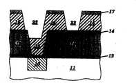
在图1-6中示出了本发明的方法的优选实施例,说明在过孔优先双镶嵌方法中本发明的使用。在图1中,方法的起点是具有其中嵌入构图导体10的半导体衬底11。可以由任何合适的导电材料形成导体10,但是优选铜形成的。在衬底11和导体10上淀积帽盖层12和层间介质(ILD)13。例如,帽盖层12可以由SiNx或SiCHN形成。可以由任何合适的介电材料形成ILD 13,但是优选低k材料形成的,即介电常数小于3.9的材料,更优选小于大约3.2。例如,低k ILD 13可以由通过等离子体增强化学汽相淀积(PECVD)淀积的SiOF(氟硅酸盐玻璃、FSG、F-TEOS等)、SiCON(有机硅酸盐玻璃、OSG碳掺杂氧化物、CDO等)或者任何其它合适的无机或有机低k介电材料形成。可以在低k材料13上增加可选的帽盖14;帽盖14可以由,例如,硅烷或TEOS氧化物材料,或者SiC(N,H)低k碳化硅形成。使用常规构图技术,例如,光刻和反应离子蚀刻(RIE)/剥离,构图过孔15。在构图过孔15期间通常不会遇到中毒,因为低k膜13还没有包含胺,或者因为帽盖14作为合适的阻挡。A preferred embodiment of the method of the present invention is shown in FIGS. 1-6 illustrating the use of the present invention in a via-first dual damascene approach. In FIG. 1 , the starting point of the method is a
然后涂覆平面化层16。平面化层16将无空隙地填充过孔15,并且对线RIE提供良好的耐受性。平面化层16还应该足够厚,以便在RIE之后有足够的厚度来定义线条图形。另外,该材料的平面化性能应该在不同过孔图形密度区域上的表面形貌中满足极限偏差,否则由于聚集深度限制,可能降低随后的高分辨率光刻性能。平面化层16的厚度可以表示为过孔高度的函数。具体地,优选在大约一半过孔高度到两倍过孔高度范围内的厚度。在优选实施例中,平面化层16对于大约140nm的过孔尺寸和大约600nm的过孔高度具有在大约200nm到大约700nm范围内的厚度。在特别优选实施例中,平面化层16具有大约450nm的厚度,其中厚度是过孔高度的大约0.75。A planarization layer 16 is then applied. The planarization layer 16 will fill the via 15 without voids and provide good resistance to wire RIE. The planarization layer 16 should also be thick enough to have enough thickness to define the line pattern after RIE. In addition, the planarization performance of the material should satisfy the limit deviation in the surface topography on regions with different via pattern densities, otherwise, the subsequent high-resolution lithography performance may be degraded due to the aggregation depth limitation. The thickness of the planarization layer 16 can be expressed as a function of via height. In particular, a thickness in the range of about half the height of the via to twice the height of the via is preferred. In a preferred embodiment, planarization layer 16 has a thickness in the range of about 200 nm to about 700 nm for a via size of about 140 nm and a via height of about 600 nm. In a particularly preferred embodiment, planarization layer 16 has a thickness of approximately 450 nm, wherein the thickness is approximately 0.75 of the via height.
平面化材料16最好是例如在美国申请No.09/256,034中用于下层的材料,其公开在此作为参考引入。具体地,平面化材料最好是聚(羟基苯乙烯)(PHS)基系,是两个PHS聚合物、交联剂和热酸发生器(TAG)的混合物。优选PHS聚合物是聚(4-羟基苯乙烯)和9-蒽基甲基化PHS(9-anthracenylmethylated PHS)。优选交联剂是四氢化-1,3,4,6-四(甲氧甲基)-咪唑并[4,5-d]咪唑-2,5-(1H,3H)-二酮,也称作“Powderlink”。优选TAG是p-硝基苄基甲苯磺酸盐(pNBT)。在该系中两个PHS聚合物聚(4-羟基苯乙烯)和9-蒽基甲基化PHS(9-anthracenylmethylated PHS)的比最好是3∶7,但是可以在0∶10到10∶0的范围之间调整,以实现所要求的光学特性。该系还包括大约10wt%(以总聚合物重量为基准)的交联剂和大约5wt%(以总聚合物重量为基准)的TAG。Planarizing material 16 is preferably a material such as that used for the underlying layers in US Application No. 09/256,034, the disclosure of which is incorporated herein by reference. Specifically, the planarizing material is preferably a poly(hydroxystyrene) (PHS) based system, a mixture of two PHS polymers, a crosslinker and a thermal acid generator (TAG). Preferred PHS polymers are poly(4-hydroxystyrene) and 9-anthracenylmethylated PHS (9-anthracenylmethylated PHS). A preferred crosslinking agent is tetrahydro-1,3,4,6-tetrakis(methoxymethyl)-imidazo[4,5-d]imidazole-2,5-(1H,3H)-dione, also known as Make "Powderlink". A preferred TAG is p-nitrobenzyl tosylate (pNBT). The ratio of the two PHS polymers poly(4-hydroxystyrene) and 9-anthracenylmethylated PHS (9-anthracenylmethylated PHS) in this system is preferably 3:7, but can be between 0:10 and 10: 0 range to achieve the required optical characteristics. The system also includes about 10 wt% (based on total polymer weight) of a crosslinker and about 5 wt% (based on total polymer weight) of TAG.
可以用作平面化材料16的其它材料包括聚芳砜,例如,BARL材料、多羟基苯乙烯基衍生物,一个例子是多羟基苯乙烯和多羟基苯乙烯与包含交联剂的蒽甲醇起反应的共聚物、以及酸催化剂(热酸发生器)、聚酰亚胺、聚醚、特别是聚芳撑醚(polyarylene醚)、聚芳撑硫醚(polyarylenesulfides)、聚碳酸酯、环氧树脂、环氧丙烯酸酯、聚芳撑(polyarylenes),例如,聚苯撑、聚芳撑亚乙烯(polyarylenevinylenes),例如,聚亚苯亚乙烯(polyphenylenevinylenes)、聚乙烯咔唑、环烯和聚酯。Other materials that may be used as planarizing material 16 include polyarylsulfones, e.g., BARL material, polyhydroxystyryl derivatives, an example being polyhydroxystyrene, and polyhydroxystyrene reacted with anthracenemethanol containing a cross-linking agent and acid catalysts (thermal acid generators), polyimides, polyethers, especially polyarylene ethers, polyarylenesulfides, polycarbonates, epoxy resins, Epoxy acrylates, polyarylenes such as polyphenylene, polyarylenevinylenes such as polyphenylenevinylenes, polyvinylcarbazoles, cycloalkenes and polyesters.
优选PHS基平面化材料最好在大约200℃到大约250℃的温度下烘焙,更优选大约225℃。Preferably, the PHS-based planarizing material is preferably baked at a temperature of about 200°C to about 250°C, more preferably about 225°C.
接着,淀积扩散阻挡层17。在优选实施例中,阻挡层17是在大约100℃到大约225℃,更优选大约150℃的温度下,使用硅烷和一氧化二氮作为淀积源,通过等离子体增强化学汽相淀积(PECVD)淀积的低温二氧化硅(LTO)。(虽然可以使用N2O,但是已经发现不导致随后的成像层中毒。)或者,能使用正硅酸乙酯(TEOS)和氧气。阻挡层17的厚度最好在大约50和100nm之间,以便作为有效的扩散阻挡。Next, a
虽然优选通过PECVD淀积LTO,但是其它材料也可以用于扩散阻挡层17,只要适当地降低它们的淀积温度和应力以避免损坏平面化层。例如,通过物理汽相淀积(溅射或蒸发)或者化学汽相淀积淀积的金属或介质可以用于扩散阻挡层17。合适的材料包括硅、氮化硅、碳化硅、氮化钛和氮化钽。层17的材料应该足够稠密以作为阻挡,并且层17应该足够薄(例如,在金属的情况下)以透光,用于光刻校准。扩散阻挡层可以由有效地阻断来自下层绝缘体的杂质,例如,可以扩散到光致抗蚀剂中的碱性杂质,扩散到光致抗蚀剂材料中并防止酸催化反应的任何材料形成。人们相信碱性杂质,例如,胺,扩散到光致抗蚀剂中并防止酸催化反应,并且LTO层将作为这些胺的阻挡。Although LTO is preferably deposited by PECVD, other materials can also be used for the
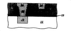
然后淀积光致抗蚀剂或成像层19,曝光并显影,由此形成沟槽20,如图1所示。在淀积成像层19之前可以淀积抗反射涂层(ARC)18。使用构图的光致抗蚀剂19作为掩模,如图2所示蚀刻ARC 18和阻挡层17,产生沟槽开口21。然后蚀刻平面化膜16,由此形成沟槽开口22,如图3所示。在蚀刻平面化层16期间,可以通过并发蚀刻除去成像层19和ARC层18,因为层19、18和16一般是在许多蚀刻化学试剂中具有同样蚀刻率的有机层。LTO层17作为蚀刻平面化层16的掩模。在图3中绘出了结果。在优选实施例中,氮和氢的混合物可用来同时蚀刻PHS基平面化层16、成像层19和ARC层18。A photoresist or imaging layer 19 is then deposited, exposed and developed, thereby forming trenches 20, as shown in FIG. An antireflective coating (ARC) 18 may be deposited prior to depositing the imaging layer 19 . Using the patterned photoresist 19 as a mask, the ARC 18 and
在图4中,使用RIE化学试剂蚀刻ILD 13,由此形成沟槽23。当ILD 13是SiCOH时,优选的RIE化学试剂是Ar/O2/CF4/CHF3和/或任何其它碳氟化合物,例如,CH3F、CH2F2、C2F6、C4F8和C5F8。在RIE步骤期间,完全除去阻挡层17,平面化层16保留在表面和过孔中。在图5中,有选择地剥离平面化层16,并且从过孔15的底部除去帽盖层12。当平面化膜16是上述优选的PHS基系时,可以使用,例如,N2/H2/O2化学试剂或O2/CO化学试剂或H化学试剂剥离。可以使用,例如,Ar/CF4/O2化学试剂或Ar/CF4/CHF3/O2化学试剂除去帽盖层12。In FIG. 4 , ILD 13 is etched using RIE chemistry, thereby forming
最后,图6描绘了双镶嵌过孔/沟槽图形的金属化,由此形成线25和过孔26。可以通过,例如,物理汽相淀积(PVD)淀积薄难熔金属衬里和Cu籽晶层,用电镀的Cu过度填充,然后通过化学机械抛光(CMP)平面化并除去多余的Cu和衬里。在CMP步骤期间,可以除去帽盖层14。在一些实施例中,不完全除去层14,而是减小到低于其原始厚度。在优选实施例中,通过CMP完全除去层14。Finally, FIG. 6 depicts the metallization of the dual damascene via/trench pattern whereby lines 25 and vias 26 are formed. A thin refractory metal liner and Cu seed layer can be deposited by, for example, physical vapor deposition (PVD), overfilled with electroplated Cu, and then planarized and removed by chemical mechanical polishing (CMP). . During the CMP step, the
例子:在90nm规程(ground rule)集成电路芯片的生产中成功地用于了在此介绍的方法,使用上述优选的PHS基系作为平面化层16,LTO作为阻挡层17。在下层Cu导体10上的帽盖层12是SiCNH,并且不后处理或使用覆盖层,以便防止由该层形成胺。一些芯片用包括N2和H2的过孔光致抗蚀剂剥离蚀刻化学试剂制造,剥离后没有清洗步骤。这将倾向于在随后225℃烘焙平面化层之后形成胺。通过光学和SEM检查并且通过电测试数据确定光致抗蚀剂没有中毒。众所周知在芯片上的某些结构对光致抗蚀剂中毒特别敏感,例如,隔离过孔和过孔链阵列测试结构的角部。显示所有测试结构完全摆脱任何光致抗蚀剂中毒作用。Example: The method presented here was successfully used in the production of integrated circuit chips of the 90nm ground rule, using the above-mentioned preferred PHS-based system as planarization layer 16 and LTO as
利用本发明的方法,消除了光致抗蚀剂中毒,并且仍然可以使用常规光刻光致抗蚀剂,不需要特殊添加剂或过程。因为晶片是完全平面化的,所以该方法允许宽的光刻工艺窗口。换句话说,不必印刷槽里面的过孔,并且不需要印刷由硬掩模产生的过多的台阶(oversteps)。此外,该方法使用常规RIE气体。不包含金属硬掩模,因此该方法与一般在半导体生产中使用的现有的后端线(BEOL)RIE工艺不矛盾,并且不包含与金属硬掩模有关的RIE生产技术的新知识。在包括Cu阻挡帽盖和层间介质本身的下层介质层的氮含量上也没有约束。因为能够调整过孔蚀刻而不影响沟槽蚀刻,所以与多硬掩模方法相比,过孔优先方法对于RIE更简单。最重要地,当引入增加多孔性和减小(deceased)物理行距的新型材料时,该方法可延伸到将来的技术。With the method of the present invention, photoresist poisoning is eliminated, and conventional photolithographic photoresists can still be used without special additives or processes. Because the wafer is fully planarized, this method allows a wide photolithographic process window. In other words, there is no need to print vias inside the trenches, and there is no need to print excessive oversteps created by the hard mask. Furthermore, this method uses conventional RIE gases. No metal hardmask is involved, so the method is not inconsistent with existing back-end-of-line (BEOL) RIE processes commonly used in semiconductor production, and does not involve new knowledge of RIE production techniques related to metal hardmasks. There is also no constraint on the nitrogen content of the underlying dielectric layer including the Cu barrier cap and the interlevel dielectric itself. The via-first approach is simpler for RIE than the multi-hardmask approach because the via etch can be tuned without affecting the trench etch. Most importantly, this approach can be extended to future technologies when new materials with increased porosity and decreased physical row spacing are introduced.
在上述优选实施例中,在过孔优先双镶嵌方法的背景中说明了本发明的方法。然而,该方法同样地适用于其它镶嵌技术,例如,线优先双镶嵌方法。In the preferred embodiment described above, the method of the present invention was described in the context of a via-first dual damascene method. However, the method is equally applicable to other damascene techniques, for example, the line-first dual damascene method.
虽然结合特定的优选实施例和其它替代实施例详细地介绍了本发明,但是很明显,根据上述说明,大量替代、改进和变化对于本领域的技术人员是显而易见的。因此,当所有这种替代、改进和变化属于本发明的真正范围时,附带的权利要求书试图包含所有这样的替代、改进和变化。While the invention has been described in detail in conjunction with certain preferred embodiments and other alternative embodiments, it is evident that numerous alternatives, modifications and variations will be apparent to those skilled in the art from the foregoing description. Therefore, it is intended to cover all such alternatives, modifications and changes in the appended claims when they fall within the true scope of the present invention.
Claims (36)
Applications Claiming Priority (2)
| Application Number | Priority Date | Filing Date | Title |
|---|---|---|---|
| US10/604,056US7030031B2 (en) | 2003-06-24 | 2003-06-24 | Method for forming damascene structure utilizing planarizing material coupled with diffusion barrier material |
| US10/604,056 | 2003-06-24 |
Publications (2)
| Publication Number | Publication Date |
|---|---|
| CN1799138A CN1799138A (en) | 2006-07-05 |
| CN100456447Ctrue CN100456447C (en) | 2009-01-28 |
Family
ID=33539867
Family Applications (1)
| Application Number | Title | Priority Date | Filing Date |
|---|---|---|---|
| CNB2004800149595AExpired - Fee RelatedCN100456447C (en) | 2003-06-24 | 2004-06-16 | Method of forming an interconnect structure in an integrated circuit device |
Country Status (8)
| Country | Link |
|---|---|
| US (2) | US7030031B2 (en) |
| EP (1) | EP1639635B1 (en) |
| JP (1) | JP4763600B2 (en) |
| KR (1) | KR100754320B1 (en) |
| CN (1) | CN100456447C (en) |
| IL (1) | IL172668A0 (en) |
| TW (1) | TWI335053B (en) |
| WO (1) | WO2004114396A1 (en) |
Families Citing this family (70)
| Publication number | Priority date | Publication date | Assignee | Title |
|---|---|---|---|---|
| US8043484B1 (en) | 2001-03-13 | 2011-10-25 | Novellus Systems, Inc. | Methods and apparatus for resputtering process that improves barrier coverage |
| US6764940B1 (en) | 2001-03-13 | 2004-07-20 | Novellus Systems, Inc. | Method for depositing a diffusion barrier for copper interconnect applications |
| US7186648B1 (en) | 2001-03-13 | 2007-03-06 | Novellus Systems, Inc. | Barrier first method for single damascene trench applications |
| US7781327B1 (en)* | 2001-03-13 | 2010-08-24 | Novellus Systems, Inc. | Resputtering process for eliminating dielectric damage |
| US8298933B2 (en) | 2003-04-11 | 2012-10-30 | Novellus Systems, Inc. | Conformal films on semiconductor substrates |
| US7842605B1 (en) | 2003-04-11 | 2010-11-30 | Novellus Systems, Inc. | Atomic layer profiling of diffusion barrier and metal seed layers |
| US7030031B2 (en)* | 2003-06-24 | 2006-04-18 | International Business Machines Corporation | Method for forming damascene structure utilizing planarizing material coupled with diffusion barrier material |
| US7196397B2 (en)* | 2004-03-04 | 2007-03-27 | International Rectifier Corporation | Termination design with multiple spiral trench rings |
| DE102004042169B4 (en)* | 2004-08-31 | 2009-08-20 | Advanced Micro Devices, Inc., Sunnyvale | Technique for increasing the filling capacity in an electrochemical deposition process by rounding the edges and trenches |
| EP1646083B1 (en) | 2004-10-08 | 2016-08-31 | Imec | Alternative dual damascene patterning approach |
| US7352064B2 (en)* | 2004-11-04 | 2008-04-01 | International Business Machines Corporation | Multiple layer resist scheme implementing etch recipe particular to each layer |
| US7371461B2 (en)* | 2005-01-13 | 2008-05-13 | International Business Machines Corporation | Multilayer hardmask scheme for damage-free dual damascene processing of SiCOH dielectrics |
| US7723008B2 (en)* | 2005-03-22 | 2010-05-25 | Intel Corporation | Photoactive adhesion promoter in a slam |
| US8598044B2 (en) | 2005-03-25 | 2013-12-03 | Renesas Electronics Corporation | Method of fabricating a semiconductor device |
| JP5186086B2 (en) | 2005-04-11 | 2013-04-17 | アイメック | Dual damascene patterning approach |
| US7857982B2 (en)* | 2005-07-19 | 2010-12-28 | Micron Technology, Inc. | Methods of etching features into substrates |
| US7289933B2 (en)* | 2005-11-04 | 2007-10-30 | Synopsys, Inc. | Simulating topography of a conductive material in a semiconductor wafer |
| US7253100B2 (en)* | 2005-11-17 | 2007-08-07 | International Business Machines Corporation | Reducing damage to ulk dielectric during cross-linked polymer removal |
| JP4533304B2 (en)* | 2005-11-29 | 2010-09-01 | 富士通セミコンダクター株式会社 | Manufacturing method of semiconductor device |
| US20070134917A1 (en)* | 2005-12-13 | 2007-06-14 | Taiwan Semiconductor Manufacturing Co., Ltd. | Partial-via-first dual-damascene process with tri-layer resist approach |
| US7485573B2 (en)* | 2006-02-17 | 2009-02-03 | International Business Machines Corporation | Process of making a semiconductor device using multiple antireflective materials |
| US7528066B2 (en) | 2006-03-01 | 2009-05-05 | International Business Machines Corporation | Structure and method for metal integration |
| US7855147B1 (en) | 2006-06-22 | 2010-12-21 | Novellus Systems, Inc. | Methods and apparatus for engineering an interface between a diffusion barrier layer and a seed layer |
| US7645696B1 (en) | 2006-06-22 | 2010-01-12 | Novellus Systems, Inc. | Deposition of thin continuous PVD seed layers having improved adhesion to the barrier layer |
| US7816069B2 (en)* | 2006-06-23 | 2010-10-19 | International Business Machines Corporation | Graded spin-on organic antireflective coating for photolithography |
| US7510634B1 (en) | 2006-11-10 | 2009-03-31 | Novellus Systems, Inc. | Apparatus and methods for deposition and/or etch selectivity |
| US20080160754A1 (en)* | 2006-12-27 | 2008-07-03 | International Business Machines Corporation | Method for fabricating a microelectronic conductor structure |
| DE102007004860B4 (en)* | 2007-01-31 | 2008-11-06 | Advanced Micro Devices, Inc., Sunnyvale | A method of making a copper-based metallization layer having a conductive overcoat by an improved integration scheme |
| US7682966B1 (en) | 2007-02-01 | 2010-03-23 | Novellus Systems, Inc. | Multistep method of depositing metal seed layers |
| US7897516B1 (en) | 2007-05-24 | 2011-03-01 | Novellus Systems, Inc. | Use of ultra-high magnetic fields in resputter and plasma etching |
| US7922880B1 (en) | 2007-05-24 | 2011-04-12 | Novellus Systems, Inc. | Method and apparatus for increasing local plasma density in magnetically confined plasma |
| CN101355047B (en)* | 2007-07-27 | 2010-05-19 | 中芯国际集成电路制造(上海)有限公司 | Method for forming through hole in low dielectric coefficient medium layer |
| US7858532B2 (en)* | 2007-08-06 | 2010-12-28 | United Microelectronics Corp. | Dielectric layer structure and manufacturing method thereof |
| US20090081864A1 (en)* | 2007-09-21 | 2009-03-26 | Texas Instruments Incorporated | SiC Film for Semiconductor Processing |
| US8084862B2 (en) | 2007-09-20 | 2011-12-27 | International Business Machines Corporation | Interconnect structures with patternable low-k dielectrics and method of fabricating same |
| US8618663B2 (en)* | 2007-09-20 | 2013-12-31 | International Business Machines Corporation | Patternable dielectric film structure with improved lithography and method of fabricating same |
| US7709370B2 (en) | 2007-09-20 | 2010-05-04 | International Business Machines Corporation | Spin-on antireflective coating for integration of patternable dielectric materials and interconnect structures |
| US7659197B1 (en) | 2007-09-21 | 2010-02-09 | Novellus Systems, Inc. | Selective resputtering of metal seed layers |
| US8136224B1 (en) | 2008-05-15 | 2012-03-20 | Western Digital (Fremont), Llc | Method and system for providing a perpendicular magnetic recording head utilizing a mask having an undercut line |
| US8017523B1 (en) | 2008-05-16 | 2011-09-13 | Novellus Systems, Inc. | Deposition of doped copper seed layers having improved reliability |
| US8084185B2 (en)* | 2009-01-08 | 2011-12-27 | International Business Machines Corporation | Substrate planarization with imprint materials and processes |
| CN102054753B (en)* | 2009-11-10 | 2013-03-13 | 中芯国际集成电路制造(上海)有限公司 | Manufacturing method for dual-inlay structure |
| US8367540B2 (en) | 2009-11-19 | 2013-02-05 | International Business Machines Corporation | Interconnect structure including a modified photoresist as a permanent interconnect dielectric and method of fabricating same |
| US8232198B2 (en) | 2010-08-05 | 2012-07-31 | International Business Machines Corporation | Self-aligned permanent on-chip interconnect structure formed by pitch splitting |
| CN101944483A (en)* | 2010-08-11 | 2011-01-12 | 上海集成电路研发中心有限公司 | Method for enhancing anti-etching capacity of photoresist |
| US8796150B2 (en) | 2011-01-24 | 2014-08-05 | International Business Machines Corporation | Bilayer trench first hardmask structure and process for reduced defectivity |
| US8900988B2 (en) | 2011-04-15 | 2014-12-02 | International Business Machines Corporation | Method for forming self-aligned airgap interconnect structures |
| US8890318B2 (en) | 2011-04-15 | 2014-11-18 | International Business Machines Corporation | Middle of line structures |
| US9054160B2 (en)* | 2011-04-15 | 2015-06-09 | International Business Machines Corporation | Interconnect structure and method for fabricating on-chip interconnect structures by image reversal |
| US8822137B2 (en) | 2011-08-03 | 2014-09-02 | International Business Machines Corporation | Self-aligned fine pitch permanent on-chip interconnect structures and method of fabrication |
| US20130062732A1 (en) | 2011-09-08 | 2013-03-14 | International Business Machines Corporation | Interconnect structures with functional components and methods for fabrication |
| US9087753B2 (en) | 2012-05-10 | 2015-07-21 | International Business Machines Corporation | Printed transistor and fabrication method |
| US20140273432A1 (en)* | 2013-03-15 | 2014-09-18 | Byung-hee Kim | Fabricating method of semiconductor device |
| US9406589B2 (en) | 2014-03-14 | 2016-08-02 | Taiwan Semiconductor Manufacturing Company, Ltd. | Via corner engineering in trench-first dual damascene process |
| US9312191B2 (en)* | 2014-08-14 | 2016-04-12 | Globalfoundries Inc. | Block patterning process for post fin |
| US9653345B1 (en)* | 2016-01-07 | 2017-05-16 | United Microelectronics Corp. | Method of fabricating semiconductor structure with improved critical dimension control |
| CN106019816B (en)* | 2016-05-16 | 2019-08-20 | 上海华力微电子有限公司 | A method of reducing photoresist poisoning |
| CN107785246B (en)* | 2016-08-30 | 2022-10-14 | 联芯集成电路制造(厦门)有限公司 | Method for ion implantation of substrate |
| US11175581B2 (en)* | 2016-12-05 | 2021-11-16 | Rohm And Haas Electronic Materials Llc | Aromatic resins for underlayers |
| US10483108B2 (en) | 2017-04-28 | 2019-11-19 | Taiwan Semiconductor Manufacturing Company, Ltd. | Semiconductor device and method of manufacture |
| US20190157213A1 (en) | 2017-11-20 | 2019-05-23 | Globalfoundries Inc. | Semiconductor structure with substantially straight contact profile |
| US10832945B2 (en) | 2019-02-15 | 2020-11-10 | International Business Machines Corporation | Techniques to improve critical dimension width and depth uniformity between features with different layout densities |
| US11251117B2 (en) | 2019-09-05 | 2022-02-15 | Intel Corporation | Self aligned gratings for tight pitch interconnects and methods of fabrication |
| US11164777B2 (en) | 2020-01-15 | 2021-11-02 | International Business Machines Corporation | Top via with damascene line and via |
| US11289375B2 (en) | 2020-03-23 | 2022-03-29 | International Business Machines Corporation | Fully aligned interconnects with selective area deposition |
| KR20210133524A (en) | 2020-04-29 | 2021-11-08 | 삼성전자주식회사 | Interconnection structure and Semiconductor package including the same |
| US11799001B2 (en) | 2021-03-09 | 2023-10-24 | Taiwan Semiconductor Manufacturing Company, Ltd. | Back-end-of-line devices |
| KR20230006737A (en)* | 2021-07-02 | 2023-01-11 | 에스케이하이닉스 주식회사 | Manufacturing method of memory device using mask patterns |
| TWI848500B (en) | 2023-01-03 | 2024-07-11 | 力晶積成電子製造股份有限公司 | Manufacturing method of semiconductor structure |
| WO2024182122A1 (en)* | 2023-02-28 | 2024-09-06 | Applied Materials, Inc. | Enhanced mobility in semiconductor devices |
Citations (7)
| Publication number | Priority date | Publication date | Assignee | Title |
|---|---|---|---|---|
| US5883006A (en)* | 1997-12-12 | 1999-03-16 | Kabushiki Kaisha Toshiba | Method for making a semiconductor device using a flowable oxide film |
| CN1258099A (en)* | 1998-12-21 | 2000-06-28 | 日本电气株式会社 | Semiconductor device interconnecting structure and mfg. method |
| JP2000208620A (en)* | 1999-01-11 | 2000-07-28 | Mitsubishi Electric Corp | Method for manufacturing semiconductor device |
| US6365529B1 (en)* | 1999-06-21 | 2002-04-02 | Intel Corporation | Method for patterning dual damascene interconnects using a sacrificial light absorbing material |
| US20020081834A1 (en)* | 2000-12-26 | 2002-06-27 | Honeywell International Inc. | Method for eliminating reaction between photoresist and OSG |
| US6469385B1 (en)* | 2001-06-04 | 2002-10-22 | Advanced Micro Devices, Inc. | Integrated circuit with dielectric diffusion barrier layer formed between interconnects and interlayer dielectric layers |
| US20030077897A1 (en)* | 2001-05-24 | 2003-04-24 | Taiwan Semiconductor Manufacturing Company | Method to solve via poisoning for porous low-k dielectric |
Family Cites Families (18)
| Publication number | Priority date | Publication date | Assignee | Title |
|---|---|---|---|---|
| JPH0513407A (en)* | 1991-03-07 | 1993-01-22 | Nec Corp | Semiconductor device and manufacturing thereof |
| JPH1197442A (en)* | 1997-09-24 | 1999-04-09 | Sony Corp | Patterning method, manufacture of semiconductor device using the same and semiconductor device thereof |
| US6297170B1 (en)* | 1998-06-23 | 2001-10-02 | Vlsi Technology, Inc. | Sacrificial multilayer anti-reflective coating for mos gate formation |
| US6316167B1 (en)* | 2000-01-10 | 2001-11-13 | International Business Machines Corporation | Tunabale vapor deposited materials as antireflective coatings, hardmasks and as combined antireflective coating/hardmasks and methods of fabrication thereof and application thereof |
| JP2000058454A (en)* | 1998-08-05 | 2000-02-25 | Sony Corp | Forming method of mask for lateral direction epitaxial growth and lateral direction epitaxial growth method |
| CN1658375B (en)* | 1999-08-26 | 2011-03-30 | 布鲁尔科技公司 | Improved filler material for use in dual damascene methods |
| JP2001230317A (en)* | 2000-02-15 | 2001-08-24 | Nec Corp | Method for forming multilayer interconnection structure and multilayer interconnection structure for semiconductor device |
| US6444408B1 (en)* | 2000-02-28 | 2002-09-03 | International Business Machines Corporation | High silicon content monomers and polymers suitable for 193 nm bilayer resists |
| JP2002050571A (en)* | 2000-05-02 | 2002-02-15 | Shipley Co Llc | Adaptation processing |
| US6426298B1 (en)* | 2000-08-11 | 2002-07-30 | United Microelectronics Corp. | Method of patterning a dual damascene |
| JP3504247B2 (en)* | 2000-12-15 | 2004-03-08 | 株式会社東芝 | Manufacturing method of semiconductor device |
| US6503840B2 (en)* | 2001-05-02 | 2003-01-07 | Lsi Logic Corporation | Process for forming metal-filled openings in low dielectric constant dielectric material while inhibiting via poisoning |
| US6855629B2 (en)* | 2002-07-24 | 2005-02-15 | Samsung Electronics Co., Ltd. | Method for forming a dual damascene wiring pattern in a semiconductor device |
| JP2003309172A (en)* | 2002-04-17 | 2003-10-31 | Nec Electronics Corp | Method of forming pattern in dual damascene process |
| US6689695B1 (en)* | 2002-06-28 | 2004-02-10 | Taiwan Semiconductor Manufacturing Company | Multi-purpose composite mask for dual damascene patterning |
| US7109119B2 (en)* | 2002-10-31 | 2006-09-19 | Taiwan Semiconductor Manufacturing Company, Ltd. | Scum solution for chemically amplified resist patterning in cu/low k dual damascene |
| US6720256B1 (en)* | 2002-12-04 | 2004-04-13 | Taiwan Semiconductor Manufacturing Company | Method of dual damascene patterning |
| US7030031B2 (en)* | 2003-06-24 | 2006-04-18 | International Business Machines Corporation | Method for forming damascene structure utilizing planarizing material coupled with diffusion barrier material |
- 2003
- 2003-06-24USUS10/604,056patent/US7030031B2/ennot_activeExpired - Lifetime
- 2004
- 2004-06-16KRKR1020057022396Apatent/KR100754320B1/ennot_activeExpired - Fee Related
- 2004-06-16CNCNB2004800149595Apatent/CN100456447C/ennot_activeExpired - Fee Related
- 2004-06-16EPEP04766050Apatent/EP1639635B1/ennot_activeExpired - Lifetime
- 2004-06-16JPJP2006516156Apatent/JP4763600B2/ennot_activeExpired - Fee Related
- 2004-06-16WOPCT/EP2004/051131patent/WO2004114396A1/enactiveSearch and Examination
- 2004-06-18TWTW093117589Apatent/TWI335053B/ennot_activeIP Right Cessation
- 2004-12-14USUS10/905,068patent/US7326651B2/ennot_activeExpired - Lifetime
- 2005
- 2005-12-18ILIL172668Apatent/IL172668A0/ennot_activeIP Right Cessation
Patent Citations (7)
| Publication number | Priority date | Publication date | Assignee | Title |
|---|---|---|---|---|
| US5883006A (en)* | 1997-12-12 | 1999-03-16 | Kabushiki Kaisha Toshiba | Method for making a semiconductor device using a flowable oxide film |
| CN1258099A (en)* | 1998-12-21 | 2000-06-28 | 日本电气株式会社 | Semiconductor device interconnecting structure and mfg. method |
| JP2000208620A (en)* | 1999-01-11 | 2000-07-28 | Mitsubishi Electric Corp | Method for manufacturing semiconductor device |
| US6365529B1 (en)* | 1999-06-21 | 2002-04-02 | Intel Corporation | Method for patterning dual damascene interconnects using a sacrificial light absorbing material |
| US20020081834A1 (en)* | 2000-12-26 | 2002-06-27 | Honeywell International Inc. | Method for eliminating reaction between photoresist and OSG |
| US20030077897A1 (en)* | 2001-05-24 | 2003-04-24 | Taiwan Semiconductor Manufacturing Company | Method to solve via poisoning for porous low-k dielectric |
| US6469385B1 (en)* | 2001-06-04 | 2002-10-22 | Advanced Micro Devices, Inc. | Integrated circuit with dielectric diffusion barrier layer formed between interconnects and interlayer dielectric layers |
Also Published As
| Publication number | Publication date |
|---|---|
| US20050079701A1 (en) | 2005-04-14 |
| KR20060011885A (en) | 2006-02-03 |
| TW200511432A (en) | 2005-03-16 |
| JP4763600B2 (en) | 2011-08-31 |
| CN1799138A (en) | 2006-07-05 |
| EP1639635B1 (en) | 2012-08-08 |
| JP2009514187A (en) | 2009-04-02 |
| US7030031B2 (en) | 2006-04-18 |
| EP1639635A1 (en) | 2006-03-29 |
| KR100754320B1 (en) | 2007-09-03 |
| IL172668A0 (en) | 2006-04-10 |
| TWI335053B (en) | 2010-12-21 |
| US7326651B2 (en) | 2008-02-05 |
| US20040266201A1 (en) | 2004-12-30 |
| WO2004114396A1 (en) | 2004-12-29 |
Similar Documents
| Publication | Publication Date | Title |
|---|---|---|
| CN100456447C (en) | Method of forming an interconnect structure in an integrated circuit device | |
| US9484248B2 (en) | Patternable dielectric film structure with improved lithography and method of fabricating same | |
| US8084862B2 (en) | Interconnect structures with patternable low-k dielectrics and method of fabricating same | |
| US6479391B2 (en) | Method for making a dual damascene interconnect using a multilayer hard mask | |
| US9035462B2 (en) | Airgap-containing interconnect structure with patternable low-k material and method of fabricating | |
| US6376366B1 (en) | Partial hard mask open process for hard mask dual damascene etch | |
| JP5186086B2 (en) | Dual damascene patterning approach | |
| US6858528B2 (en) | Composite sacrificial material | |
| US9196523B2 (en) | Self-aligned permanent on-chip interconnect structures | |
| US20050037605A1 (en) | Method of forming metal interconnection layer of semiconductor device | |
| US7268071B2 (en) | Dual damascene interconnections having low K layer with reduced damage arising from photoresist stripping | |
| JP2009532866A (en) | Damascene interconnect having a porous low-k layer with improved mechanical properties | |
| US20070222076A1 (en) | Single or dual damascene structure reducing or eliminating the formation of micro-trenches arising from lithographic misalignment | |
| US6150232A (en) | Formation of low k dielectric | |
| US7300868B2 (en) | Damascene interconnection having porous low k layer with a hard mask reduced in thickness | |
| US20070232062A1 (en) | Damascene interconnection having porous low k layer followed by a nonporous low k layer | |
| US20030205815A1 (en) | Fabrication method of integrated circuits with borderless vias and low dielectric constant inter-metal dielectrics | |
| US20250140605A1 (en) | Interconnect structure with high thermal conductivity and low parasitic capacitance |
Legal Events
| Date | Code | Title | Description |
|---|---|---|---|
| C06 | Publication | ||
| PB01 | Publication | ||
| C10 | Entry into substantive examination | ||
| SE01 | Entry into force of request for substantive examination | ||
| C14 | Grant of patent or utility model | ||
| GR01 | Patent grant | ||
| TR01 | Transfer of patent right | ||
| TR01 | Transfer of patent right | Effective date of registration:20171115 Address after:Grand Cayman, Cayman Islands Patentee after:GLOBALFOUNDRIES INC. Address before:American New York Patentee before:Core USA second LLC Effective date of registration:20171115 Address after:American New York Patentee after:Core USA second LLC Address before:American New York Patentee before:International Business Machines Corp. | |
| CF01 | Termination of patent right due to non-payment of annual fee | ||
| CF01 | Termination of patent right due to non-payment of annual fee | Granted publication date:20090128 Termination date:20190616 |