CN100454375C - Light emitting device and driving method thereof - Google Patents
Light emitting device and driving method thereofDownload PDFInfo
- Publication number
- CN100454375C CN100454375CCNB021318220ACN02131822ACN100454375CCN 100454375 CCN100454375 CCN 100454375CCN B021318220 ACNB021318220 ACN B021318220ACN 02131822 ACN02131822 ACN 02131822ACN 100454375 CCN100454375 CCN 100454375C
- Authority
- CN
- China
- Prior art keywords
- pixel
- luminescent device
- current value
- vision signal
- light emitting
- Prior art date
- Legal status (The legal status is an assumption and is not a legal conclusion. Google has not performed a legal analysis and makes no representation as to the accuracy of the status listed.)
- Expired - Fee Related
Links
Images


Classifications
- G—PHYSICS
- G09—EDUCATION; CRYPTOGRAPHY; DISPLAY; ADVERTISING; SEALS
- G09G—ARRANGEMENTS OR CIRCUITS FOR CONTROL OF INDICATING DEVICES USING STATIC MEANS TO PRESENT VARIABLE INFORMATION
- G09G3/00—Control arrangements or circuits, of interest only in connection with visual indicators other than cathode-ray tubes
- G09G3/20—Control arrangements or circuits, of interest only in connection with visual indicators other than cathode-ray tubes for presentation of an assembly of a number of characters, e.g. a page, by composing the assembly by combination of individual elements arranged in a matrix no fixed position being assigned to or needed to be assigned to the individual characters or partial characters
- G09G3/2007—Display of intermediate tones
- G09G3/2059—Display of intermediate tones using error diffusion
- G—PHYSICS
- G09—EDUCATION; CRYPTOGRAPHY; DISPLAY; ADVERTISING; SEALS
- G09G—ARRANGEMENTS OR CIRCUITS FOR CONTROL OF INDICATING DEVICES USING STATIC MEANS TO PRESENT VARIABLE INFORMATION
- G09G3/00—Control arrangements or circuits, of interest only in connection with visual indicators other than cathode-ray tubes
- G09G3/20—Control arrangements or circuits, of interest only in connection with visual indicators other than cathode-ray tubes for presentation of an assembly of a number of characters, e.g. a page, by composing the assembly by combination of individual elements arranged in a matrix no fixed position being assigned to or needed to be assigned to the individual characters or partial characters
- G09G3/22—Control arrangements or circuits, of interest only in connection with visual indicators other than cathode-ray tubes for presentation of an assembly of a number of characters, e.g. a page, by composing the assembly by combination of individual elements arranged in a matrix no fixed position being assigned to or needed to be assigned to the individual characters or partial characters using controlled light sources
- G09G3/30—Control arrangements or circuits, of interest only in connection with visual indicators other than cathode-ray tubes for presentation of an assembly of a number of characters, e.g. a page, by composing the assembly by combination of individual elements arranged in a matrix no fixed position being assigned to or needed to be assigned to the individual characters or partial characters using controlled light sources using electroluminescent panels
- G09G3/32—Control arrangements or circuits, of interest only in connection with visual indicators other than cathode-ray tubes for presentation of an assembly of a number of characters, e.g. a page, by composing the assembly by combination of individual elements arranged in a matrix no fixed position being assigned to or needed to be assigned to the individual characters or partial characters using controlled light sources using electroluminescent panels semiconductive, e.g. using light-emitting diodes [LED]
- G09G3/3208—Control arrangements or circuits, of interest only in connection with visual indicators other than cathode-ray tubes for presentation of an assembly of a number of characters, e.g. a page, by composing the assembly by combination of individual elements arranged in a matrix no fixed position being assigned to or needed to be assigned to the individual characters or partial characters using controlled light sources using electroluminescent panels semiconductive, e.g. using light-emitting diodes [LED] organic, e.g. using organic light-emitting diodes [OLED]
- G09G3/3225—Control arrangements or circuits, of interest only in connection with visual indicators other than cathode-ray tubes for presentation of an assembly of a number of characters, e.g. a page, by composing the assembly by combination of individual elements arranged in a matrix no fixed position being assigned to or needed to be assigned to the individual characters or partial characters using controlled light sources using electroluminescent panels semiconductive, e.g. using light-emitting diodes [LED] organic, e.g. using organic light-emitting diodes [OLED] using an active matrix
- G09G3/3233—Control arrangements or circuits, of interest only in connection with visual indicators other than cathode-ray tubes for presentation of an assembly of a number of characters, e.g. a page, by composing the assembly by combination of individual elements arranged in a matrix no fixed position being assigned to or needed to be assigned to the individual characters or partial characters using controlled light sources using electroluminescent panels semiconductive, e.g. using light-emitting diodes [LED] organic, e.g. using organic light-emitting diodes [OLED] using an active matrix with pixel circuitry controlling the current through the light-emitting element
- G—PHYSICS
- G09—EDUCATION; CRYPTOGRAPHY; DISPLAY; ADVERTISING; SEALS
- G09G—ARRANGEMENTS OR CIRCUITS FOR CONTROL OF INDICATING DEVICES USING STATIC MEANS TO PRESENT VARIABLE INFORMATION
- G09G2300/00—Aspects of the constitution of display devices
- G09G2300/08—Active matrix structure, i.e. with use of active elements, inclusive of non-linear two terminal elements, in the pixels together with light emitting or modulating elements
- G09G2300/0809—Several active elements per pixel in active matrix panels
- G09G2300/0842—Several active elements per pixel in active matrix panels forming a memory circuit, e.g. a dynamic memory with one capacitor
- G—PHYSICS
- G09—EDUCATION; CRYPTOGRAPHY; DISPLAY; ADVERTISING; SEALS
- G09G—ARRANGEMENTS OR CIRCUITS FOR CONTROL OF INDICATING DEVICES USING STATIC MEANS TO PRESENT VARIABLE INFORMATION
- G09G2310/00—Command of the display device
- G09G2310/02—Addressing, scanning or driving the display screen or processing steps related thereto
- G09G2310/0243—Details of the generation of driving signals
- G09G2310/0251—Precharge or discharge of pixel before applying new pixel voltage
- G—PHYSICS
- G09—EDUCATION; CRYPTOGRAPHY; DISPLAY; ADVERTISING; SEALS
- G09G—ARRANGEMENTS OR CIRCUITS FOR CONTROL OF INDICATING DEVICES USING STATIC MEANS TO PRESENT VARIABLE INFORMATION
- G09G2320/00—Control of display operating conditions
- G09G2320/02—Improving the quality of display appearance
- G—PHYSICS
- G09—EDUCATION; CRYPTOGRAPHY; DISPLAY; ADVERTISING; SEALS
- G09G—ARRANGEMENTS OR CIRCUITS FOR CONTROL OF INDICATING DEVICES USING STATIC MEANS TO PRESENT VARIABLE INFORMATION
- G09G2320/00—Control of display operating conditions
- G09G2320/02—Improving the quality of display appearance
- G09G2320/0257—Reduction of after-image effects
- G—PHYSICS
- G09—EDUCATION; CRYPTOGRAPHY; DISPLAY; ADVERTISING; SEALS
- G09G—ARRANGEMENTS OR CIRCUITS FOR CONTROL OF INDICATING DEVICES USING STATIC MEANS TO PRESENT VARIABLE INFORMATION
- G09G2320/00—Control of display operating conditions
- G09G2320/02—Improving the quality of display appearance
- G09G2320/0285—Improving the quality of display appearance using tables for spatial correction of display data
- G—PHYSICS
- G09—EDUCATION; CRYPTOGRAPHY; DISPLAY; ADVERTISING; SEALS
- G09G—ARRANGEMENTS OR CIRCUITS FOR CONTROL OF INDICATING DEVICES USING STATIC MEANS TO PRESENT VARIABLE INFORMATION
- G09G2320/00—Control of display operating conditions
- G09G2320/02—Improving the quality of display appearance
- G09G2320/029—Improving the quality of display appearance by monitoring one or more pixels in the display panel, e.g. by monitoring a fixed reference pixel
- G09G2320/0295—Improving the quality of display appearance by monitoring one or more pixels in the display panel, e.g. by monitoring a fixed reference pixel by monitoring each display pixel
- G—PHYSICS
- G09—EDUCATION; CRYPTOGRAPHY; DISPLAY; ADVERTISING; SEALS
- G09G—ARRANGEMENTS OR CIRCUITS FOR CONTROL OF INDICATING DEVICES USING STATIC MEANS TO PRESENT VARIABLE INFORMATION
- G09G2320/00—Control of display operating conditions
- G09G2320/04—Maintaining the quality of display appearance
- G09G2320/043—Preventing or counteracting the effects of ageing
- G—PHYSICS
- G09—EDUCATION; CRYPTOGRAPHY; DISPLAY; ADVERTISING; SEALS
- G09G—ARRANGEMENTS OR CIRCUITS FOR CONTROL OF INDICATING DEVICES USING STATIC MEANS TO PRESENT VARIABLE INFORMATION
- G09G2340/00—Aspects of display data processing
- G09G2340/14—Solving problems related to the presentation of information to be displayed
- G—PHYSICS
- G09—EDUCATION; CRYPTOGRAPHY; DISPLAY; ADVERTISING; SEALS
- G09G—ARRANGEMENTS OR CIRCUITS FOR CONTROL OF INDICATING DEVICES USING STATIC MEANS TO PRESENT VARIABLE INFORMATION
- G09G3/00—Control arrangements or circuits, of interest only in connection with visual indicators other than cathode-ray tubes
- G09G3/20—Control arrangements or circuits, of interest only in connection with visual indicators other than cathode-ray tubes for presentation of an assembly of a number of characters, e.g. a page, by composing the assembly by combination of individual elements arranged in a matrix no fixed position being assigned to or needed to be assigned to the individual characters or partial characters
- G09G3/22—Control arrangements or circuits, of interest only in connection with visual indicators other than cathode-ray tubes for presentation of an assembly of a number of characters, e.g. a page, by composing the assembly by combination of individual elements arranged in a matrix no fixed position being assigned to or needed to be assigned to the individual characters or partial characters using controlled light sources
- G09G3/30—Control arrangements or circuits, of interest only in connection with visual indicators other than cathode-ray tubes for presentation of an assembly of a number of characters, e.g. a page, by composing the assembly by combination of individual elements arranged in a matrix no fixed position being assigned to or needed to be assigned to the individual characters or partial characters using controlled light sources using electroluminescent panels
- G09G3/32—Control arrangements or circuits, of interest only in connection with visual indicators other than cathode-ray tubes for presentation of an assembly of a number of characters, e.g. a page, by composing the assembly by combination of individual elements arranged in a matrix no fixed position being assigned to or needed to be assigned to the individual characters or partial characters using controlled light sources using electroluminescent panels semiconductive, e.g. using light-emitting diodes [LED]
- G09G3/3208—Control arrangements or circuits, of interest only in connection with visual indicators other than cathode-ray tubes for presentation of an assembly of a number of characters, e.g. a page, by composing the assembly by combination of individual elements arranged in a matrix no fixed position being assigned to or needed to be assigned to the individual characters or partial characters using controlled light sources using electroluminescent panels semiconductive, e.g. using light-emitting diodes [LED] organic, e.g. using organic light-emitting diodes [OLED]
- G09G3/3275—Details of drivers for data electrodes
- G09G3/3291—Details of drivers for data electrodes in which the data driver supplies a variable data voltage for setting the current through, or the voltage across, the light-emitting elements
Landscapes
- Engineering & Computer Science (AREA)
- Physics & Mathematics (AREA)
- Computer Hardware Design (AREA)
- General Physics & Mathematics (AREA)
- Theoretical Computer Science (AREA)
- Electroluminescent Light Sources (AREA)
- Control Of Indicators Other Than Cathode Ray Tubes (AREA)
- Control Of El Displays (AREA)
Abstract
Description
Translated fromChinese技术领域technical field
本发明涉及到发光器件,其中的发光元件和用来控制此发光元件的晶体管被提供在半导体衬底或绝缘表面上,本发明还涉及到驱动发光器件的方法。更具体地说,本发明涉及到发光器件及其驱动方法,其中消除了控制发光元件的晶体管的特性起伏的影响。本发明属于有关采用诸如晶体管之类的半导体元件的发光器件的技术领域。The present invention relates to a light emitting device in which a light emitting element and a transistor for controlling the light emitting element are provided on a semiconductor substrate or an insulating surface, and to a method of driving the light emitting device. More specifically, the present invention relates to a light emitting device and a driving method thereof, in which influence of characteristic fluctuation of a transistor controlling a light emitting element is eliminated. The present invention belongs to the technical field related to light emitting devices using semiconductor elements such as transistors.
背景技术Background technique
近年来,采用发光元件的发光器件(图象显示器件)的发展正在取得进展。发光器件大致分成无源型和有源型。有源型发光器件各在绝缘表面上具有发光元件和用来控制此发光元件的晶体管。In recent years, the development of light emitting devices (image display devices) using light emitting elements is progressing. Light emitting devices are roughly classified into passive types and active types. Active type light emitting devices each have a light emitting element and a transistor for controlling the light emitting element on an insulating surface.
采用多晶硅膜的晶体管的场效应迁移率(也称为迁移率)高于由非晶硅膜制作的常规晶体管的迁移率,因而能够比由非晶硅膜制作的晶体管在更高的速度下工作。因此,能够利用与象素制作在同一个绝缘表面上的驱动电路来进行对象素的控制,而在常规情况下则是利用衬底外部的驱动电路来进行的。这种有源发光器件具有各种优点,包括生产成本降低、尺寸减小、成品率上升、以及借助于在同一个绝缘表面上建立各种各样的电路和元件而得到的产率改善。Transistors using polysilicon films have higher field-effect mobility (also called mobility) than conventional transistors made of amorphous silicon films, and thus can operate at higher speeds than transistors made of amorphous silicon films . Thus, control of the pixels can be performed using drive circuits fabricated on the same insulating surface as the pixels, which is conventionally performed using drive circuits external to the substrate. Such active light emitting devices have various advantages including reduced production cost, reduced size, increased yield, and improved yield by building various circuits and components on the same insulating surface.
有源发光器件的大多数驱动方法是模拟方法和数字方法。模拟方法对流入发光元件的电流进行控制,以控制亮度并获得灰度。另一方面,数字方法借助于仅仅在发光元件处于开通状态(其亮度几乎是100%)的开通态和发光元件处于关断状态(其亮度几乎为0)的关断态之间进行转换而驱动器件。这只能得到二个灰度,因此,对于数字方法,已经提出了借助于将其与时间灰度方法和面积比灰度等进行组合而获得多灰度的技术。Most driving methods of active light emitting devices are analog methods and digital methods. The analog method controls the current flowing into the light-emitting element to control the brightness and obtain the gray scale. On the other hand, the digital method drives by switching only between an on state in which the light emitting element is on (its brightness is almost 100%) and an off state in which the light emitting element is in an off state (its brightness is almost 0%) device. This can only obtain two gray scales, and therefore, for the digital method, a technique of obtaining multiple gray scales by combining it with a time gray scale method, an area ratio gray scale, etc. has been proposed.
现在参照图14以及图15A和15B来详细描述发光器件的驱动方法。首先参照图1 4来描述发光器件的结构。图1 4示出了发光器件中象素部分1800的电路图例子。将馈自栅信号线驱动电路的栅信号传送到象素的栅信号线(G1-Gy),被连接到开关晶体管的栅电极。开关晶体管被提供在各个象素中,并用1801表示。各个象素的开关晶体管1801具有源区和漏区,其中之一被连接到用来输入视频信号的源信号线(S1-Sx)之一,而另一被连接到各个象素的驱动晶体管1804的栅电极和各个象素的电容器1808。A driving method of the light emitting device will now be described in detail with reference to FIG. 14 and FIGS. 15A and 15B. First, the structure of the light emitting device will be described with reference to FIG. 14 . FIG. 14 shows an example of a circuit diagram of a
各个象素的驱动晶体管1804具有连接到电源线(V1-Vx)之一的源区,并具有连接到发光元件1806的漏区。电源线(V1-Vx)的电位被称为电源电位。各个电源线(V1-Vx)被连接到各个象素的电容器1808。The
发光元件1806具有阳极、阴极、以及插入在阳极与阴极之间的有机化合物层。若发光元件1806的阳极被连接到驱动晶体管1804的漏区,则阳极用作象素电极,而发光元件1806的阴极用作反电极。另一方面,若发光元件1806的阴极被连接到驱动晶体管1804的漏区,则发光元件1806的阳极用作反电极,而阴极用作象素电极。The
反电极的电位被称为反电位,而为反电极提供反电位的电源被称为反电源。象素电极的电位与反电极的电位之差,就是驱动电压,且此驱动电压被施加到有机化合物层。The potential of the counter electrode is called the counter potential, and the power source that provides the counter potential to the counter electrode is called the counter power supply. The difference between the potential of the pixel electrode and the potential of the counter electrode is the driving voltage, and this driving voltage is applied to the organic compound layer.
图15A和15B是当图14的发光器件被模拟方法驱动时的时间图。在图15A和15B中,从选择一个栅信号线开始到选择下一个栅信号线结束的周期,被称为一行周期(L)。从一个图象被显示开始到下一个图象被显示结束的周期被称为一帧周期(F)。图14的发光器件具有y个栅信号线,因此,在一个帧周期中提供了y个行周期(L1-Ly)。15A and 15B are time charts when the light emitting device of FIG. 14 is driven by an analog method. In FIGS. 15A and 15B, the period from when one gate signal line is selected to when the next gate signal line is selected is referred to as a row period (L). The period from when one image is displayed to when the next image is displayed is called a frame period (F). The light emitting device of FIG. 14 has y gate signal lines, therefore, y line periods (L1-Ly) are provided in one frame period.
电源线(V1-Vx)被保持在恒定的电源电位下。反电位即反电极的电位也被保持恒定。反电位被设置成其与电源电位之差大得足以使发光元件发光。The power supply lines (V1-Vx) are kept at a constant power supply potential. The counter potential, ie the potential of the counter electrode, is also kept constant. The counter potential is set so that its difference from the power supply potential is large enough to cause the light emitting element to emit light.
在第一行周期(L1)中,栅信号线(G1)被馈自栅信号线驱动电路的栅信号选择。栅信号线被选择意味着其栅电极被连接到此栅信号线的晶体管被开通。In the first row period (L1), the gate signal line (G1) is selected by the gate signal fed from the gate signal line driving circuit. A gate signal line being selected means that a transistor whose gate electrode is connected to this gate signal line is turned on.
模拟视频信号被依次输入到源信号线(S1-Sx)。由于被连接到栅信号线(G1)的各个开关晶体管1801被开通,故输入到源信号线(S1-Sx)的视频信号,通过开关晶体管1801被输入到驱动晶体管1804的栅电极。Analog video signals are sequentially input to the source signal lines (S1-Sx). Since each
驱动晶体管1804的沟道形成区中流动的电流量,被输入到驱动晶体管1804的栅电极的信号的电位(电压)电平控制。因此,施加到发光元件1806的象素电极的电位电平决定于输入到驱动晶体管1804的栅电极的视频信号的电位电平。简言之,电流以相应于视频信号电位电平的量而在发光元件1806中流动,发光元件1806从而根据此电流量而发光。The amount of current flowing in the channel formation region of the driving
上述的操作被重复,直至完成对源信号线(S1-Sx)的视频信号输入。这是第一行周期(L1)的终点。然后开始第二行周期(L2),栅信号线(G2)被栅信号选择。相似于第一行周期(L1),视频信号被依次输入到源信号线(S1-Sx)。The above-described operations are repeated until the video signal input to the source signal lines (S1-Sx) is completed. This is the end of the first line period (L1). Then the second row period (L2) starts, and the gate signal line (G2) is selected by the gate signal. Similar to the first line period (L1), video signals are sequentially input to the source signal lines (S1-Sx).
上述的操作被重复,直至完成对所有栅信号线(G1-Gy)的栅信号输入,从而结束一帧周期。在一帧周期中,所有的象素被用来形成显示图象。The above-described operations are repeated until the gate signal input to all the gate signal lines (G1-Gy) is completed, thereby ending one frame period. During one frame period, all pixels are used to form a display image.
如上所述,采用视频信号来控制流入到发光元件中的电流量,且其中的灰度相应于此电流量而被确定的方法,是一种被称为模拟类型的驱动方法。简言之,在模拟驱动方法中,根据输入到象素的视频信号的电位而确定灰度。As described above, a method in which a video signal is used to control the amount of current flowing into a light-emitting element, and in which gradation is determined corresponding to the amount of current, is a driving method called an analog type. In short, in the analog driving method, gradation is determined according to the potential of a video signal input to a pixel.
另一方面,如上所述,在数字驱动方法中,利用与时间灰度方法等的组合,得到了多灰度。在与时间灰度方法组合的数字驱动方法中,根据电流在发光元件的二个电极之间流动的周期的长度来确定灰度(其详细的时间图未提供)。On the other hand, as described above, in the digital driving method, multi-gradation is obtained by combining with the time gray-scale method or the like. In the digital driving method combined with the time gray scale method, the gray scale is determined according to the length of a period in which current flows between two electrodes of the light emitting element (the detailed time chart thereof is not provided).
下面参照图11A-13所述的是驱动晶体管1804和发光元件1806的电压-电流特性。图11A仅仅示出了图14所示象素中的驱动晶体管1804和发光元件1806。图11B示出了图11A的驱动晶体管1804和发光元件1806的电压-电流特性。图11B中的驱动晶体管1804的电压-电流特性曲线示出了与源区与漏区之间的电压VDS相关的流动在驱动晶体管1804的漏区中的电流量。图12示出了驱动晶体管1804的源区与栅电极之间的电压VGS彼此不同的多个电压-电流特性曲线。Described below with reference to FIGS. 11A-13 are the voltage-current characteristics of the
如图11A所示,施加在发光元件1806的象素电极与反电极之间的电压被给定为VEL,而施加在连接到电源线的端子3601与发光元件1806的反电极之间电压被给定为VT。VT的数值被电源线(V1-Vx)的电位固定。VDS表示驱动晶体管1804的源区与漏区之间的电压,而VGS表示连接到驱动晶体管1804的栅电极的布线3602与源区之间的电压,亦即驱动晶体管1804的栅电极与源区之间的电压。As shown in FIG. 11A, the voltage applied between the pixel electrode and the counter electrode of the
驱动晶体管1804和发光元件1806被彼此串联连接。这意味着相同的电流量在元件(驱动晶体管1804和发光元件1806)中流动。因此,图11A所示的驱动晶体管1804和发光元件1806在表示元件电压-电流特性的曲线的交叉点(工作点)处被驱动。在图11B中,VEL对应于反电极1809的电位与工作点处的电位之间的电压。VDS对应于驱动晶体管1804在端子3601处的电位与1804在工作点处的电位之间的电压。因此,VT等于VEL与VDS之和。The driving
此处考虑VGS被改变的情况。如从图11B可见,随着驱动晶体管1804的|VGS-VTH|的增大,换言之,随着|VGS|的增大,流入到驱动晶体管1804中的电流量也增大。VTH表示驱动晶体管1804的阈值电压。因此,如图11B所示,|VGS|的增大自然随之以在工作点处流入到发光元件1806中的电流量的增大。发光元件1806的亮度正比于流入到发光元件1806中的电流量而增大。A case where VGS is changed is considered here. As can be seen from FIG. 11B , as |VGS −VTH | of the driving
当流入到发光元件1806中的电流量伴随|VGS |的上升而增大时,VEL因而增大。当VEL增大时,因为VT被是一个被电源线(V1-Vx)的电位确定的固定数值,故VDS减小同等幅度。When the amount of current flowing into the
如图11B所示,驱动晶体管1804的电压-电流特性曲线能够被VGS和VDS的数值分成二个范围。|VGS-VTH|<|VDS|的一个范围是饱和区,而|VGS-VTH|>|VDS|的一个范围是线性区。As shown in FIG. 11B , the voltage-current characteristic curve of the driving
在饱和区内,下列数学表达式(1)被满足。IDS被给定为流入到驱动晶体管1804的沟道形成区中的电流量。β=μC0W/L,其中μ表示驱动晶体管1804的迁移率,C0表示单位面积的栅电容,而W/L表示沟道形成区的沟道宽度W对其沟道长度L的比率。In the saturation region, the following mathematical expression (1) is satisfied. IDS is given as the amount of current flowing into the channel formation region of the
[数学表达式1][mathematical expression 1]
IDS=β(VGS-VTH)2 ......(1)IDS =β(VGS -VTH )2 ......(1)
在线性区中,下列数学表达式(2)被满足。In the linear region, the following mathematical expression (2) is satisfied.
[数学表达式2][mathematical expression 2]
IDS=β{(VGS-VTH)VDS-VDS2} ......(2)IDS =β{(VGS -VTH )VDS -VDS2 } ......(2)
从数学表达式(1)可见,饱和区内的电流量很难被VDS改变,而仅仅决定于VGS。It can be seen from the mathematical expression (1) that the current in the saturation region is hardly changed by VDS and is only determined by VGS .
从数学表达式(2)可见,线性区内的电流量决定于VDS和VGS。随着|VGS|的增大,驱动晶体管1804开始工作于线性区。VEL也逐渐增大。因此,VDS减小,其减小量与VEL的增大量相同。当VDS减小时,线性区内的电流量也减小。因此,尽管|VGS|增大,电流量却不容易增大。但|VGS|=∞时,电流量达到IMAX。换言之,无论|VGS|多么大,也不流动大于IMAX的电流。IMAX表示VEL=VT时在发光元件1806中流动的电流量。It can be seen from the mathematical expression (2) that the amount of current in the linear region is determined by VDS and VGS . As |VGS | increases, the driving
借助于以这种方式对|VGS|的电平进行控制,工作点能够被移动到饱和区或移动到线性区。By controlling the level of |VGS | in this way, the operating point can be shifted into the saturation region or into the linear region.
理想地说,每个驱动晶体管1804具有相同的特性。但实际上,各个驱动晶体管1804之间的阈值电压VTH和迁移率μ常常变化。当各个驱动晶体管1804之间的阈值电压VTH和迁移率μ变化时,如数学表达式(1)和(2)所示,即使VGS相同,驱动晶体管1804沟道区这流动的电流量也要起伏。Ideally, each
图12示出了其阈值电压VTH和迁移率μ偏离于理想情况的驱动晶体管1804的电压-电流特性。实线3701表示理想电压-电流特性曲线。3702和3703各表示其阈值电压VTH和迁移率μ偏离于理想情况的驱动晶体管1804的电压-电流特性。FIG. 12 shows the voltage-current characteristics of the
饱和区内的电压-电流特性曲线3702和3703偏离于理想电流-电压曲线3701相同的电流量ΔIA。电压-电流特性曲线3702的工作点3705处于饱和区内,而电压-电流特性曲线3703的工作点3706处于线性区内。在此情况下,工作点3705处的电流量和工作点3706处的电流量偏离于理想电压-电流特性曲线3701在工作点3704处的电流量分别为ΔIB和ΔIC。线性区内工作点3706处的ΔIC小于饱和区内工作点3705处的ΔIB。The voltage-current characteristic curves 3702 and 3703 in the saturation region deviate from the ideal current-voltage curve 3701 by the same current amount ΔIA . The operating point 3705 of the voltage-current characteristic curve 3702 is in the saturation region, and the operating point 3706 of the voltage-current characteristic curve 3703 is in the linear region. In this case, the amount of current at operating point 3705 and the amount of current at operating point 3706 deviate from the ideal voltage-current characteristic curve 3701 at operating point 3704 by ΔIB and ΔIC , respectively. ΔIC at operating point 3706 in the linear region is less than ΔIB at operating point 3705 in the saturation region.
总结上述的工作分析,图13示出了驱动晶体管1804的电流量相对于栅电压|VGS|的曲线。当|VGS|增大,直至超过驱动晶体管1804的阈值电压的绝对值|VTH|时,驱动晶体管1804被开通,电流开始流动。若|VGS|进一步增大,则|VGS|达到满足|VGS-VTH|=|VGS|的数值(此处,用A表示此数值),且曲线离开饱和区而进入线性区。若|VGS|继续进一步增大,则电流量增大且最终达到饱和。此时|VGS|=∞。Summarizing the above-described operational analysis, FIG. 13 shows a graph of the amount of current driving the
如从图13可见,在|VGS |≤|VTH|的范围内,几乎没有电流流动。满足|VTH|≤|VGS|≤A的范围被称为饱和区,在此范围内,电流量被|VGS|改变。这意味着,若在饱和区中施加到发光元件1806的电压即使被稍许改变,发光元件1806中流动的电流量也指数地改变。发光元件1806的亮度几乎正比于发光元件1806中流动的电流量而上升。总之,在根据|VGS|而控制流入发光元件中的电流量的模拟驱动方法中,器件主要工作于饱和区,以便控制亮度并获得灰度。As can be seen from FIG. 13 , in the range of |VGS |≤|VTH |, almost no current flows. A range satisfying |VTH |≤|VGS |≤A is called a saturation region, and within this range, the amount of current is changed by |VGS |. This means that if the voltage applied to the
另一方面,图13中A≤|VGS|的范围是线性区,在此范围内,流入到发光元件的电流量被|VGS|和|VDS|改变。在线性区中,当施加到发光元件1806的电压电平被改变时,流入到发光元件1806中的电流量不太改变。数字驱动方法借助于仅仅在发光元件处于开通(其亮度几乎为100%)的开通态与发光元件处于关断(其亮度几乎为0%)的关断态二种状态之间进行转化而驱动器件。当器件工作于A≤|VGS|的范围以便开通发光元件时,电流数值必定接近IMAX,且发光元件的亮度达到几乎100%。另一方面,当器件工作于|VTH|≥|VGS|的范围以便关断发光元件时,电流数值几乎为0,且发光元件的亮度达到几乎0%。简言之,由数字方法驱动的发光器件主要工作于|VTH|≥|VGS|和A≤|VGS|的范围内。On the other hand, the range of A≦|VGS | in FIG. 13 is a linear region in which the amount of current flowing into the light emitting element is changed by |VGS | and |VDS |. In the linear region, when the voltage level applied to the
在由模拟方法驱动的发光器件中,当开关晶体管被开通时,输入到象素模拟视频信号转变成驱动晶体管的栅电压。此时,驱动晶体管漏区的电位根据输入到驱动晶体管栅电极的模拟视频信号的电压而被确定,且给定的漏电流流入到发光元件。发光元件以相应于漏电流的量(亮度)发光。如上所述,发光元件的光发射量被控制,从而获得灰度显示。In a light emitting device driven by an analog method, when a switching transistor is turned on, an analog video signal input to a pixel is converted into a gate voltage of a driving transistor. At this time, the potential of the drain region of the driving transistor is determined according to the voltage of the analog video signal input to the gate electrode of the driving transistor, and a given leakage current flows into the light emitting element. The light emitting element emits light with an amount (brightness) corresponding to the leakage current. As described above, the light emission amount of the light emitting element is controlled so that gray scale display is obtained.
然而,上述的模拟方法的缺点是其抗驱动晶体管特性起伏的能力非常差。利用各个象素的特性起伏的驱动晶体管,即使当相同电平的栅电压被施加到各个驱动晶体管时,也不可能馈送相同量的漏电流。换言之,即使发光元件接受相同电压电平的视频信号,各个驱动晶体管中的特性的稍许起伏也引起发光元件发射光量大幅度变化的光。However, the disadvantage of the above-mentioned analog method is that it is very poor against fluctuations in the characteristics of the drive transistor. With the driving transistors whose characteristics fluctuate for each pixel, it is impossible to feed the same amount of leakage current even when the same level of gate voltage is applied to the respective driving transistors. In other words, even if the light-emitting elements receive video signals of the same voltage level, slight fluctuations in characteristics in the respective drive transistors cause the light-emitting elements to emit light whose light quantity greatly varies.
模拟驱动方法于是对驱动晶体管之间的特性起伏很敏感,并且是用常规有源发光器件进行灰度显示的一个不利条件。The analog driving method is then sensitive to characteristic fluctuations between the driving transistors and is a disadvantage of grayscale display with conventional active light-emitting devices.
若发光器件被数字方法驱动以便处置驱动晶体管之间的特性起伏,则伴随着有机化合物层的退化,流入到发光元件的有机化合物层中的电流量被改变。If the light emitting device is driven by a digital method in order to deal with fluctuations in characteristics between driving transistors, the amount of current flowing into the organic compound layer of the light emitting element is changed along with the degradation of the organic compound layer.
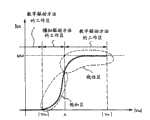
这是因为发光元件随着老化而自然退化。图18A的曲线示出了发光元件在退化之前和之后的电压-电流特性曲线。在数字驱动方法中,如上所述,发光器件工作于线性区。当发光元件退化时,其电压-电流特性曲线如图18A所示被改变,使其工作点被偏移。这就引起发光元件二个电极之间流动的电流量的改变。This is because light emitting elements naturally degrade with aging. The graphs of FIG. 18A show voltage-current characteristic curves of the light-emitting element before and after degradation. In the digital driving method, as described above, the light emitting device operates in the linear region. When the light-emitting element degrades, its voltage-current characteristic curve is changed as shown in FIG. 18A, so that its operating point is shifted. This causes a change in the amount of current flowing between the two electrodes of the light emitting element.
发明内容Contents of the invention
考虑到上述问题而提出了本发明,因此,本发明的目的是提供一种发光器件及其驱动方法,其中的发光器件用模拟方法来驱动,并消除了晶体管之间特性起伏的影响以获得清晰的多灰度显示。本发明的另一目的是提供以此发光器件作为其显示器件的电子设备。The present invention has been made in consideration of the above-mentioned problems, and therefore, an object of the present invention is to provide a light-emitting device and a driving method thereof in which the light-emitting device is driven by an analog method and the influence of fluctuations in characteristics between transistors is eliminated to obtain clear multi-grayscale display. Another object of the present invention is to provide electronic equipment using the light emitting device as its display device.
本发明的再一目的是提供一种发光器件及其驱动方法,其中在发光元件二个电极之间流动的电流量随老化的变化被减小,以便获得清晰的多灰度显示。本发明的还一目的是提供以此发光器件作为其显示器件的电子设备。Another object of the present invention is to provide a light-emitting device and its driving method, wherein the variation of the amount of current flowing between two electrodes of the light-emitting element with aging is reduced so as to obtain clear multi-gray scale display. Another object of the present invention is to provide an electronic device using the light-emitting device as its display device.
根据上述情况,本发明提供了一种发光器件及其驱动方法,其中借助于对提供在象素中的驱动晶体管的特性进行规定,以及借助于根据特性规定而修正待要输入到象素的视频信号,来消除驱动晶体管之间特性起伏的影响。In view of the foregoing, the present invention provides a light emitting device and a driving method thereof, wherein by specifying the characteristics of a driving transistor provided in a pixel, and by correcting the video signal to be input to the pixel according to the regulation of the characteristics signal to eliminate the influence of characteristic fluctuations between drive transistors.
本发明利用了下列事实,即发光元件的发光量(亮度)受流入到发光元件中的电流量的控制。换言之,若发光元件接收所希望的电流量,就有可能使发光元件以所希望的量发光。因此,适合于各个象素的驱动晶体管特性的视频信号被输入到各个象素,致使所希望的电流量流入到各个发光元件中。以这种方式,发光元件能够以所希望的量发光,而不受驱动晶体管之间特性起伏的影响。The present invention utilizes the fact that the amount of light emitted (brightness) of a light emitting element is controlled by the amount of current flowing into the light emitting element. In other words, if the light emitting element receives a desired amount of current, it is possible to cause the light emitting element to emit light in a desired amount. Therefore, a video signal suitable for the characteristics of the driving transistor of each pixel is input to each pixel, so that a desired amount of current flows into each light emitting element. In this way, the light emitting element can emit light in a desired amount without being affected by fluctuations in characteristics between driving transistors.
下面描述的是本发明的关键,即驱动晶体管特性的规定方法。首先,安培表被连接到向发光元件馈送电流的引线,以便测量流入到发光元件中的电流。例如,安培表被连接到向发光元件馈送电流的引线,例如电源线或反电源线,并测量流入到发光元件中的电流。在测量电流的过程中,要确保视频信号从源信号线驱动电路仅仅被输入到特定的象素(最好是一个象素,但也可以是多个特定的象素)而没有电流在其它象素的发光元件中流动。以这种方式,安培表能够测量仅仅在特定象素中流动的电流。若不同电压值的视频信号被输入,则能够对各个象素测量与不同电压值相关的多个电流值。What is described below is the crux of the invention, namely the prescribed method of driving the characteristics of the transistor. First, an ammeter is connected to a lead wire that feeds current to the light emitting element in order to measure the current flowing into the light emitting element. For example, an ammeter is connected to a lead that feeds current to the light-emitting element, such as a power line or a counter-power line, and measures the current flowing into the light-emitting element. In the process of measuring the current, it is necessary to ensure that the video signal from the source signal line driver circuit is only input to a specific pixel (preferably one pixel, but it can also be a plurality of specific pixels) and no current flows in other pixels. Flow in the light-emitting element of the element. In this way, the ammeter is able to measure the current flowing only in specific pixels. If video signals of different voltage values are input, a plurality of current values associated with different voltage values can be measured for each pixel.
在本发明中,用P(P1,P2,...,Pn,n是至少等于或大于2的自然数)表示视频信号。借助于计算显示平板中的每个象素不发光时的电流值I0与显示平板中只有一个象素发光时的电流值I1,I2,...,In之间的差别,而得到对应于视频信号P(P1,P2,...,Pn)的电流值Q(Q1,Q2,...,Qn)。对各个象素得到P和Q,以便用插入法获得象素的特性。插入法是一种用来获得在函数的二个或更多个点处函数值之间一个点的近似的计算方法,或一种借助于在二个点之间的一个点处提供(插入)函数值而展开函数的方法。用来提供近似的表达式被称为插入表达式,示于表达式(3)。In the present invention, a video signal is represented by P (P1 , P2 , . . . , Pn , n is a natural number at least equal to or greater than 2). By means of calculating the difference between the current value I0 when each pixel in the display panel does not emit light and the current value I1 , I2 , ..., In when only one pixel in the display panel emits light,and A current value Q(Q1 , Q2 , . . . , Qn ) corresponding to the video signal P(P1 , P2 , . . . , Pn ) is obtained. P and Q are obtained for each pixel to obtain the characteristics of the pixel by interpolation. Interpolation is a computational method used to obtain an approximation of a point between the value of a function at two or more points of a function, or a method of calculation by providing (interpolation) at a point between two points A method to expand a function by its value. The expression used to provide the approximation is called an interpolation expression, shown in expression (3).
[数学表达式3][mathematical expression 3]
Q=F(P) ......(3)Q=F(P) ...(3)
借助于用对各个象素测得的视频信号P(P1,P2,...,Pn)的值和对应于视频信号的电流值Q(Q1,Q2,...,Qn)替换数学表达式(3)中的P和Q,来获得插入函数F。得到的插入函数F被存储在提供于发光器件中的诸如半导体存储器或磁性存储器之类的存储媒质中。By using the value of the video signal P(P1 , P2 , ..., Pn ) measured for each pixel and the current value Q (Q1 , Q2 , ..., Qn ) to replace P and Q in the mathematical expression (3) to obtain the interpolation function F. The obtained interpolation function F is stored in a storage medium such as a semiconductor memory or a magnetic memory provided in the light emitting device.
为了使发光器件显示一个图象,用存储在存储媒质中的插入函数F来计算适合于各个象素的驱动晶体管特性的视频信号(P)。当得到的视频信号(P)被输入到象素时,所希望的电流量就在各个发光元件中流动,从而得到所希望的亮度。In order for the light emitting device to display an image, the interpolation function F stored in the storage medium is used to calculate the video signal (P) suitable for the characteristics of the driving transistor of each pixel. When the obtained video signal (P) is input to a pixel, a desired amount of current flows in each light emitting element, thereby obtaining a desired luminance.
根据本发明的发光器件的定义包括:具有发光元件和驱动电路的象素部分被密封在衬底与覆盖元件之间的显示平板(发光屏)、借助于将IC等安装到显示平板而得到的发光模块、以及用作显示器件的发光显示器。换言之,“发光器件”是发光平板、发光模块、发光显示器的通用术语。发光元件不是本发明不可缺少的组成部分,在本说明书中,不包括发光元件的器件也被称为发光器件。The definition of a light emitting device according to the present invention includes: a display panel (light emitting panel) in which a pixel portion having a light emitting element and a driving circuit is sealed between a substrate and a cover element, obtained by mounting an IC or the like to a display panel A light emitting module, and a light emitting display used as a display device. In other words, "light emitting device" is a general term for light emitting panels, light emitting modules, and light emitting displays. The light emitting element is not an indispensable component of the present invention, and in this specification, a device that does not include a light emitting element is also referred to as a light emitting device.
根据本发明,提供了包括具有象素的显示平板的发光器件,各个象素包括发光元件,此器件的特征是包含:According to the present invention, there is provided a light-emitting device comprising a display panel having pixels, each pixel comprising a light-emitting element, the device is characterized by comprising:
用来测量象素的电流值的电流测量装置;A current measuring device for measuring the current value of the pixel;
利用由电流测量装置输出的电流值来计算对应于象素的插入函数的计算装置;calculating means for calculating an interpolation function corresponding to a pixel using the current value output by the current measuring means;
用来存储各个象素的插入函数的存储装置;以及storage means for storing the interpolation function for each pixel; and
利用存储在存储装置中的插入函数来修正视频信号的信号修正装置。Signal modification means for modifying video signals using an interpolation function stored in storage means.
电流测量装置具有用来测量发光元件二个电极之间流动的电流的装置,相当于例如安培表或由电阻元件和电容器元件组成的利用电阻分配来测量电流的电路。计算装置和信号修正装置具有进行计算的装置,相当于例如微计算机或CPU。存储装置相当于诸如半导体存储器或磁性存储器之类的熟知的存储媒质。象素的不发光状态指的是象素的发光元件不发光的状态,亦即其中被输入“黑色”图象信号的象素的状态。象素的发光状态指的是象素的发光元件发光的状态,亦即其中被输入“白色”图象信号的象素的状态。The current-measuring device has means for measuring the current flowing between the two electrodes of the light-emitting element, corresponding to, for example, an ammeter or a circuit consisting of a resistance element and a capacitor element for measuring the current by resistance distribution. The calculation means and the signal correction means have means for calculation, and correspond to, for example, a microcomputer or a CPU. The storage device corresponds to a well-known storage medium such as a semiconductor memory or a magnetic memory. The non-light-emitting state of a pixel refers to a state in which a light-emitting element of a pixel does not emit light, that is, a state of a pixel into which an image signal of "black" is input. The light-emitting state of a pixel refers to a state in which a light-emitting element of a pixel emits light, that is, a state of a pixel into which a "white" image signal is input.
根据本发明,提供了一种驱动具有显示平板的发光器件的方法,此方法的特征是包含:According to the present invention, a method for driving a light-emitting device with a display panel is provided, the method is characterized by comprising:
测量显示平板中每个象素不发光时的电流值I0;Measure the current value I0 when each pixel in the display panel does not emit light;
测量视频信号P1,P2,...,Pn(n是自然数)被输入到显示平板的象素时的电流值I1,I2,...,In;Measure the current value I1 , I2 , ..., In when the video signal P1 , P2 ,... , Pn (n is a natural number) is input to the pixel of the display panel;
利用是为电流值I0与电流值I1,I2,...,In之间的差别的Q1,Q2,...,Qn、视频信号P1,P2,...,Pn、以及插入表达式Q=F(P),计算插入函数F;以及UtilizingQ 1,Q2, ..., Q n,video signals P1 , P2 , .. ., Pn , and the interpolation expression Q=F(P), calculate the interpolation function F; and
利用插入函数F,修正输入到显示平板的象素的视频信号。Using the interpolation function F, the video signals input to the pixels of the display panel are corrected.
本发明中的象素的典型结构包括用来控制发光元件二个电极之间流动的电流的第一半导体元件、用来控制视频信号到象素的输入的第二半导体元件、以及用来保持视频信号的电容器元件。半导体元件相当于晶体管或具有开关功能的其它元件。电容器元件具有保持电荷的功能,其材料没有特别的限制。The typical structure of the pixel in the present invention includes a first semiconductor element used to control the current flowing between the two electrodes of the light-emitting element, a second semiconductor element used to control the input of the video signal to the pixel, and a second semiconductor element used to hold the video signal. signal capacitor element. A semiconductor element corresponds to a transistor or other element having a switching function. The capacitor element has a function of holding charges, and its material is not particularly limited.
如上所述构成的本发明能够提供发光器件及其驱动方法,其中用模拟方法来驱动发光器件,并消除了晶体管之间特性起伏的影响,从而获得清晰的多灰度显示。而且,本发明能够提供发光器件及其驱动方法,其中减小了发光元件二个电极之间流动的电流量随老化的变化,从而获得清晰的多灰度显示。The present invention constituted as described above can provide a light-emitting device and a driving method thereof in which the light-emitting device is driven by an analog method and the influence of fluctuations in characteristics between transistors is eliminated, thereby obtaining clear multi-gradation display. Furthermore, the present invention can provide a light emitting device and a driving method thereof, in which the variation with aging of the amount of current flowing between two electrodes of the light emitting element is reduced, thereby obtaining clear multi-gray scale display.
附图说明Description of drawings
在附图中:In the attached picture:
图1是本发明的发光器件的电路图;Fig. 1 is the circuit diagram of light-emitting device of the present invention;
图2是本发明的发光器件的电路图;Fig. 2 is the circuit diagram of the light-emitting device of the present invention;
图3A和3B示出了根据本发明的发光器件的驱动方法;3A and 3B illustrate a driving method of a light emitting device according to the present invention;
图4A-4D是输入到本发明的发光器件的信号的时间图;4A-4D are timing diagrams of signals input to the light emitting device of the present invention;
图5示出了视频信号与电流值之间的关系;Fig. 5 shows the relationship between the video signal and the current value;
图6是本发明的发光器件中的象素的电路图;Fig. 6 is the circuit diagram of the pixel in the light-emitting device of the present invention;
图7示出了本发明的发光器件的剖面结构(向下发射);Fig. 7 shows the cross-sectional structure (downward emission) of the light emitting device of the present invention;
图8A-8C示出了本发明的发光器件,其中图8A示出了器件外部;8A-8C show the light emitting device of the present invention, wherein FIG. 8A shows the outside of the device;
图9示出了本发明的发光器件的外部;Fig. 9 shows the exterior of the light emitting device of the present invention;
图10A-10H示出了具有本发明的发光器件的电子设备的例子;10A-10H show an example of an electronic device with a light emitting device of the present invention;
图11A和11B分别为示出了发光元件与驱动晶体管的连接结构的视图,和示出了发光元件与驱动晶体管的电压-电流特性的视图;11A and 11B are views showing a connection structure of a light emitting element and a driving transistor, and views showing voltage-current characteristics of a light emitting element and a driving transistor, respectively;
图12示出了发光元件与驱动晶体管的电压-电流特性;Figure 12 shows the voltage-current characteristics of the light-emitting element and the driving transistor;
图13示出了驱动晶体管的栅电压与漏电流之间的关系;Figure 13 shows the relationship between the gate voltage of the drive transistor and the drain current;
图14是发光器件的象素部分的电路图;14 is a circuit diagram of a pixel portion of a light emitting device;
图15A和15B是输入到发光器件的信号的时间图;15A and 15B are timing diagrams of signals input to a light emitting device;
图16示出了视频信号与电流值之间的关系;Fig. 16 shows the relationship between the video signal and the current value;
图17A和17B示出了本发明的发光器件的剖面结构(向上发射);而17A and 17B show the cross-sectional structure (upward emission) of the light-emitting device of the present invention; and
图18A-18C示出了发光元件和驱动晶体管的电压-电流特性以及象素的电路图。18A-18C show voltage-current characteristics of a light emitting element and a driving transistor and a circuit diagram of a pixel.
具体实施方式Detailed ways
实施方案模式Implementation mode
下面参照图1-5来描述本发明的实施方案模式。Embodiment modes of the present invention are described below with reference to FIGS. 1-5.
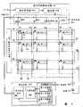
图1是发光器件的电路图例子。在图1中,发光器件具有象素部分103、以及被安排在象素部分103外围的源信号线驱动电路101和栅信号线驱动电路102。图1的发光器件具有一个源信号线驱动电路101和一个栅信号线驱动电路102,但本发明不局限于此。取决于象素100的结构,可以随意设定源信号线驱动电路101和栅信号线驱动电路102的数目。FIG. 1 is an example of a circuit diagram of a light emitting device. In FIG. 1 , the light emitting device has a
源信号线驱动电路101具有移位寄存器101a、缓冲器101b、以及取样电路101c。但本发明不局限于此,101可以具有保持电路等。The source signal
时钟信号(CLK)和起始脉冲(SP)被输入到移位寄存器101a。响应于时钟信号(CLK)和起始脉冲(SP),移位寄存器101a顺序产生时间信号,这些时间信号通过缓冲器101b被顺序输入到取样电路101c。A clock signal (CLK) and a start pulse (SP) are input to the shift register 101a. In response to a clock signal (CLK) and a start pulse (SP), the shift register 101a sequentially generates time signals, which are sequentially input to the sampling circuit 101c through the buffer 101b.
馈自移位寄存器101a的时间信号被缓冲器101b缓冲并放大。时间信号被输入其中的布线,被连接到许多电路或元件,因而具有大的负载电容。缓冲器101b被提供来避免大负载电容引起的时间信号的迟钝升降。The time signal fed from the shift register 101a is buffered and amplified by the buffer 101b. The wiring, into which the timing signal is input, is connected to many circuits or elements, and thus has a large load capacitance. A buffer 101b is provided to avoid sluggish rise and fall of the timing signal caused by large load capacitances.
取样电路101c响应于从缓冲器101b输入的时间信号而将视频信号顺序输出到象素100。取样电路101c具有视频信号线125和取样线(SA1-SAx)。注意,本发明不局限于这种结构,101c可以具有模拟开关或其它的半导体元件。The sampling circuit 101c sequentially outputs video signals to the
象素部分103具有源信号线(S1-Sx)、栅信号线(G1-Gy)、电源线(V1-Vx)、以及反电源线(E1-Ey)。多个象素100被排列在象素部分103中,使之形成矩阵图形。The
电源线(V1-Vx)通过安培表130被连接到电源131。安培表130和电源131可以被形成在不同于其上形成象素部分103的衬底上,通过连接件等被连接到象素部分103。作为变通,如果有可能的话,130和131可以被形成在与形成象素部分103的衬底相同的衬底上。安培表130的数目和电源131的数目没有特别的限制,可以随意设定。若安培表130被连接到向发光元件111供应电流的布线,就足够了。例如,安培表130可以被连接到反电源线(E1-Ey)。简言之,安培表130的位置没有特别的限制。安培表130相当于测量装置。The power lines ( V1 - Vx ) are connected to a power source 131 through an
安培表130测得的电流值作为数据被送到修正电路210。修正电路210具有存储媒质(存储装置)211、计算电路(计算装置)202、以及信号修正电路(信号修正装置)204。信号修正电路210的结构不局限于图1所示的,210可以具有放大电路、转换电路等。如有需要,修正电路210可以仅仅具有存储媒质211。可以随意设定修正电路210的结构。The current value measured by the
存储媒质211具有第一存储器200、第二存储器201、以及第三存储器203。但本发明不局限于此,存储器的数目可以由设计者随意设定。诸如ROM、RAM、快速存储器、或磁带之类的熟知存储媒质能够被用作存储媒质211。当存储媒质211与其上放置象素部分的衬底集成时,最好用半导体存储器特别是ROM作为存储媒质211。若本发明的发光器件被用作计算机的显示器件,则存储媒质211可以被提供在计算机中。The storage medium 211 has a
计算电路202具有计算措施。更具体地说,计算电路202具有从电流值I1,I2,...,In减去象素部分103不发光时的电流值I0而计算电流值Q1,Q2,...,Qn的计算措施。计算电路202具有从在视频信号P1,P2,...,Pn被输入到象素100时的电流值Q1,Q2,...,Qn计算上述表达式(3)的插入函数的措施。熟知的计算电路或微计算机能够被用作计算电路202。若本发明的发光器件被用作计算机的显示器件,则计算电路202可以被提供在计算机中。The
信号修正电路204具有修正视频信号的措施。更具体地说,204具有利用存储在各个象素100的存储媒质211中的插入函数F和上述表达式(3)而修正输入到象素100的视频信号的措施。熟知的信号修正电路、微计算机等能够被用作信号修正电路204。若本发明的发光器件被用作计算机的显示器件,则信号修正电路204可以被提供在计算机中。The
源信号线(S1-Sx)通过取样晶体管126被连接到视频信号线125。取样晶体管126具有源区和漏区,其中之一被连接到源信号线S(S1-Sx之一),另一被连接到视频信号线125。取样晶体管126的栅电极被连接到取样线SA(SA1-Sax之一)。The source signal lines ( S1 - Sx ) are connected to the video signal line 125 through the
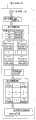
图2示出了一个象素100,即行j和列i上的一个象素的放大图。在此象素(i,j)中,111表示发光元件,112表示开关晶体管,113表示驱动晶体管,而114表示电容器。Figure 2 shows an enlarged view of a
开关晶体管112的栅电极被连接到栅信号线(Gj)。开关晶体管112具有源区和漏区,其中之一被连接到源信号线(Si),另一被连接到驱动晶体管113的栅电极。开关晶体管112是在信号被输入到象素(i,j)时用作开关元件的晶体管。如图1所示而不是如图2所示,其上连接开关晶体管112的源信号线(Si),通过取样晶体管126被连接到视频信号线125。The gate electrode of the switching
电容器114被提供来保持开关晶体管112不被选择(关断状态)时的驱动晶体管113的栅电压。虽然本实施方案模式采用了电容器114,但本发明不局限于此。电容器114可以被略去。The
驱动晶体管113的源区被连接到电源线(Vi),而113的漏区被连接到发光元件111。电源线(Vi)通过安培表130被连接到电源131,并接收恒定的电源电位。电源线Vi还被连接到电容器114。驱动晶体管113是用作控制馈送到发光元件111的电流的元件(电流控制元件)的晶体管。The source region of the driving
发光元件111由阳极、阴极、以及插入在阳极与阴极之间的有机化合物层组成。若阳极被连接到驱动晶体管113的漏区,则阳极用作象素电极,而阴极用作反电极。另一方面,若阴极被连接到驱动晶体管113的漏区,则阴极用作象素电极,而阳极用作反电极。The
发光元件被构造成有机化合物层被夹在一对电极(阳极和阴极)之间。有机化合物层可以由熟知的发光材料组成。存在着二种有机化合物层结构:单层结构和多层结构。二种结构都可以采用。有机化合物层的发光被分成从单重激发态返回到基态时的发光(荧光)和从三重激发态返回到基态时的发光(磷光)。二种发光都可以作用。A light-emitting element is constructed such that an organic compound layer is sandwiched between a pair of electrodes (anode and cathode). The organic compound layer can be composed of well-known luminescent materials. There are two types of organic compound layer structures: a single layer structure and a multilayer structure. Both structures can be used. The light emission of the organic compound layer is divided into light emission (fluorescence) when the singlet excited state returns to the ground state and light emission (phosphorescence) when the triplet excited state returns to the ground state. Both kinds of light can work.
发光元件的反电极被连接到反电源121。反电源121的电位被称为反电位。象素电极的电位与反电极电位之差,是施加到有机化合物层的驱动电压。The counter electrode of the light emitting element is connected to a counter power source 121 . The potential of the counter power source 121 is called a counter potential. The difference between the potential of the pixel electrode and the potential of the counter electrode is the driving voltage applied to the organic compound layer.
接着,参照图3A来描述根据本发明的有关对提供在各个象素100中的驱动晶体管113的特性进行规定以及基于图1和2所示发光器件中的规定而修正待要输入到各个象素100的视频信号的方法。为了使解释易于理解,此方法的各个阶段被称为步骤1-步骤5。图3B示出了修正电路210,在图3A和3B之间可进行交叉参考。Next, referring to FIG. 3A , description will be made regarding the specification of the characteristics of the
图4A-4D是从提供在发光器件中的驱动电路(源信号线驱动电路101和栅信号线驱动电路102)输出的信号的时间图。由于象素部分103具有y个栅信号线,故在一帧周期中提供了y个行周期(L1-Ly)。4A-4D are timing charts of signals output from driving circuits (source signal
图4A示出了借助于在一行周期(L)中反复选择一个栅信号线G(G1-Gy之一)而完成y个栅信号线(G1-Gy)的选择之后,如何度过一帧周期。图4B示出了借助于同时反复选择一个取样线SA(SA1-SAx之一)而完成所有x个取样线(SA1-SAx)的选择之后,如何度过一行周期。图4C示出了在步骤1中视频信号P0如何被输入到源信号线(S1-Sx)。图4D示出了在步骤2中视频信号P1,P2,P3和P0如何被输入到源信号线(S1-Sx)。4A shows how to spend a frame period after the selection of y gate signal lines (G1-Gy) is completed by repeatedly selecting a gate signal line G (one of G1-Gy) in a row period (L). . FIG. 4B shows how one line period passes after selection of all x sampling lines (SA1-SAx) is completed by repeatedly selecting one sampling line SA (one of SA1-SAx) simultaneously. Fig. 4C shows how the video signalP0 is input to the source signal lines (S1-Sx) in
首先,在步骤1中,使象素部分103处于全黑状态。全黑状态指的是每个发光元件111都停止发光的状态,亦即没有象素发光的状态。图4C示出了在步骤1中视频信号P0如何被输入到源信号线(S1-Sx)。在图4C中,视频信号P0仅仅在一行周期中被输入到源信号线(S1-Sx)。实际上,视频信号P0在一帧周期(F)中提供的所有行周期(L1-Ly)中被输入到源信号线。当在一帧周期中完成将相同的视频信号P0输入到所有象素100时,提供在象素部分103中的每个发光元件111就停止发光(全黑状态)。First, in
在达到这一状态之后,用安培表130测量电源线(V1-Vx)中流动的电流值I0。此时测得的电流值I0相当于若在发光元件111的阳极与阴极之间存在着短路,或在某些象素100中存在着短路,或若FPC未被牢固地连接到象素部分103时,意外流动的电流值。测得的电流值I0被存储在提供于连接电路210中的第一存储器200中,从而结束步骤1。After reaching this state, the value I0 of the current flowing in the power line (V1-Vx) is measured with the
接着,在步骤2中,不同的视频信号P1,P2,P3和P0被输入到提供在象素部分103中的象素100。Next, in
在本实施方案模式中,如图4D所示,4个彼此台阶状变换的视频信号P1,P2,P3和P0被输入到源信号线(S1-Sx)。简言之,在一行周期(L)中,4个视频信号P1,P2,P3和P0被输入到象素100之一,并借助于重复此操作,在一帧周期(F)中,4个视频信号P1,P2,P3和P0被输入到象素部分103中的所有象素100。In this embodiment mode, as shown in FIG. 4D, four video signalsP1 ,P2 ,P3, andP0 that are stepped into each other are input to the source signal lines (S1-Sx). In short, in one line period (L), four video signals P1 , P2 , P3 and P0 are input to one of the
然后,响应于3个视频信号P1,P2,P3,流入驱动晶体管113中亦即电源线(V1-Vx)中的电流值被安培表130测量。Then, the value of the current flowing into the driving
虽然在本实施方案模式中,在一行周期(L)中,4个彼此台阶状变换的视频信号P1,P2,P3和P0被输入到一个象素,但本发明不局限于此。例如,可以在一行周期(L)中仅仅输入视频信号P1,以便在下一个行周期(L)中输入视频信号P2,再在下一个行周期中输入视频信号P3。在本实施方案模式中输入的4个视频信号P1,P2,P3和P0被彼此台阶状变换。但在本发明中,若电压值不同的视频信号被输入以测量与电压值不同的视频信号相关的电流值,就足够了。例如,彼此以斜坡状方式(如锯齿)变换的视频信号可以被输入,以便用安培表130以规则的间距测量多个电流值。Although in this embodiment mode, four video signals P1 , P2 , P3 and P0 that are transformed stepwise from each other are input to one pixel in one line period (L), the present invention is not limited thereto. . For example, only the video signal P1 may be input in one line period (L), so that the video signal P2 is input in the next line period (L), and the video signal P3 is input in the next line period. The four video signalsP1 ,P2 ,P3 andP0 input in this embodiment mode are transformed into each other stepwise. However, in the present invention, it is sufficient if video signals having different voltage values are input to measure the current value associated with the video signals having different voltage values. For example, video signals transformed with each other in a ramp-like manner (eg, sawtooth) may be input to measure a plurality of current values at regular intervals with the
现在,作为例子来描述第j行上的栅信号线(Gj)被馈自栅信号线驱动电路102的栅信号选择的情况。在一行周期(Lj)中,4个视频信号P1,P2,P3和P0被输入到象素(1,j),象素(1,j)之外的象素因而都被关断。因此,安培表130测得的电流值是在特定象素(1,j)的驱动晶体管113中流动的电流值与步骤1中测得的电流值I0之和。然后,在象素(1,j)中测量分别与P1,P2,P3相关的电流值I1,I2,I3,且测得的电流值I1,I2,I3被存储在第二存储器201中。Now, a case where the gate signal line (Gj) on the j-th row is selected by the gate signal fed from the gate signal line drive circuit 102 will be described as an example. In one line period (Lj), 4 video signals P1 , P2 , P3 and P0 are input to the pixel (1, j), and the pixels other than the pixel (1, j) are thus turned off. broken. Therefore, the current value measured by the
接着,视频信号P0被输入到象素(1,j),以使象素(1,j)的发光元件111停止发光,致使象素(1,j)不再发光。这是为了防止电流在测量下一个象素(2,j)的过程中流动。Next, the video signalP0 is input to the pixel (1, j), so that the
然后,4个视频信号P1,P2,P3和P0被输入到象素(2,j)。分别与视频信号P1,P2,P3相关的电流值I1,I2,I3,被获得并存储在第二存储器201中。Then, four video signals P1 , P2 , P3 and P0 are input to the pixel (2,j). The current values I1 , I2 , I3 associated with the video signals P1 , P2 , P3 , respectively, are obtained and stored in the second memory 201 .
以这种方式重复上述操作,直至完成将视频信号输入到行j和列1-x上的象素。换言之,当视频信号到所有源信号线(S1-Sx)的输入结束时,就结束了一行周期Lj。The above operations are repeated in this manner until the input of video signals to the pixels on row j and columns 1-x is completed. In other words, when the input of the video signal to all the source signal lines (S1-Sx) ends, the one-line period Lj ends.
然后开始下一个行周期Lj+1,栅信号线Gj+1被馈自栅信号线驱动电路102的栅信号选择。然后,4个视频信号P1,P2,P3和P0被输入到每一个源信号线(S1-Sx)。Then the next row period Lj+1 starts, and the gate signal line Gj+1 is selected by the gate signal fed from the gate signal line driving circuit 102 . Then, 4 video signals P1 , P2 , P3 and P0 are input to each source signal line (S1-Sx).
重复上述操作,直至完成将栅信号输入到所有栅信号线(G1-Gy)。这就完成了所有的行周期(L1-Ly)。当所有行周期(L1-Ly)被完成时,一帧周期就结束。The above operations are repeated until the input of gate signals to all gate signal lines (G1-Gy) is completed. This completes all line periods (L1-Ly). A frame period ends when all line periods (L1-Ly) are completed.
以这种方式,分别与输入到象素部分103中的象素100的3个视频信号P1,P2,P3相关的电流值I1,I2,I3就被测量。获得的数据被存储在第二存储器201中。In this way, current valuesI1 ,I2 ,I3 respectively associated with the three video signalsP1 ,P2 , P3 input to the
从对象素部分103中各个象素100测得的电流值I1,I2,I3,计算电路202计算其与步骤1中存储在第一存储器200中的电流值I0之差。于是得到电流值Q1,Q2和Q3。于是得到下列表达式。From the current valuesI1 ,I2 ,I3 measured for the
Q1=I1-I0Q1 =I1 -I0
Q2=I2-I0Q2 =I2 -I0
Q3=I3-I0Q3 =I3 -I0
电流值Q1,Q2和Q3被存储在第二存储器201中,从而结束步骤2。The current values Q1 , Q2 and Q3 are stored in the second memory 201 , thus ending
若象素部分103没有短路的象素,且若FPC被牢固地连接到象素部分103,则测得的电流值I0为0或几乎为0。在此情况下,可以略去对象素部分103中各个象素100的从电流值I1,I2,I3减去电流值I0的操作以及测量电流值I0的操作。这些操作可以是可选的。If the
在步骤3中,计算电路202利用上述表达式(1)计算各个象素的驱动晶体管的电流-电压特性(IDS-VGS特性)。若表达式(1)中的IDS、VGS、VTH分别是I、P、B,且Q1=I1-I0,则得到下列表达式(4)。In Step 3, the
[数学表达式4][mathematical expression 4]
Q=A*(P-B)2 ......(4)Q=A*(PB)2 ......(4)
在表达式(4)中,A和B各为常数。当已知至少二组数据(P,Q)时,能够得到常数A和常数B。详细地说,借助于用已经在步骤2中得到的至少二个电压值不同的视频信号(P)以及与此视频信号(P)相关的至少二个电流值(Q)替换表达式(3)中的变量,能够获得常数A和常数B。常数A和常数B被存储在第三存储器203中。In Expression (4), A and B are each constants. When at least two sets of data (P, Q) are known, constant A and constant B can be obtained. In detail, by replacing expression (3) with at least two video signals (P) having different voltage values obtained in
使具有一定电流值(Q)的电流流动所需的视频信号(P)的电压值,能够从存储在第三存储器203中的常数A和常数B得到。此计算使用了下列表达式(5)。The voltage value of the video signal (P) required to flow a current having a certain current value (Q) can be obtained from the constant A and the constant B stored in the
[数学表达式5][mathematical expression 5]
P=(Q/A)1/2+BP=(Q/A)1/2 +B
={(I-I0)/A}1/2+B ......(5)={(II0 )/A}1/2 +B ......(5)
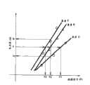
此处给出了一个例子,并用表达式(4)和(5)计算了象素D、E、F的常数A和常数B。结果被示于图5。如图5所示,当同一视频信号(作为例子,此处是视频信号P2)被输入到象素D、E、F时,Iq所示的电流在象素D中流动,Ir所示的电流在象素E中流动,而Ip所示的电流在象素F中流动。即使输入相同的视频信号(P2),由于提供在象素D、E、F中的晶体管的特性彼此不同,各个象素D、E、F中的电流值仍然变化。本发明借助于利用上述表达式(4)来输入适合于各个象素100特性的视频信号,消除了特性起伏的这种影响。An example is given here, and constant A and constant B of pixels D, E, F are calculated using expressions (4) and (5). The results are shown in Figure 5. As shown in FIG. 5, when the same video signal (here, video signal P2 as an example) is input to pixels D, E, and F, a current shown by Iq flows in pixel D, and a current shown by Ir Flows in pixel E, while the current indicated by Ip flows in pixel F. Even if the same video signal (P2 ) is input, since the characteristics of the transistors provided in the pixels D, E, F are different from each other, the current values in the respective pixels D, E, F still vary. The present invention eliminates such influence of characteristic fluctuation by inputting a video signal suitable for the characteristic of each
虽然在图5中,利用表达式(4)和(5),象素D、E、F中的特性被表示为二次曲线,但本发明不局限于次。图16示出了一些曲线,其中利用下列表达式(6),输入到象素D、E、F的视频信号(P)和与此视频信号(P)相关的电流值(Q)之间的关系被表示为直线。Although in FIG. 5, the characteristics in pixels D, E, F are expressed as quadratic curves using expressions (4) and (5), the present invention is not limited to quadratic curves. Fig. 16 shows curves in which the difference between the video signal (P) input to the pixels D, E, F and the current value (Q) related to this video signal (P) is obtained using the following expression (6). Relationships are represented as straight lines.
[数学表达式6][mathematical expression 6]
Q=a*P+B ......(6)Q=a*P+B ......(6)
借助于用步骤2中对各个象素得到的电压值(P)和电流值(Q)替换表达式(6)中的变量,计算了常数a和常数b。得到的常数a和常数b被存储在各个象素100的第三存储器203中,从而结束步骤3。Constant a and constant b are calculated by substituting the variables in expression (6) with the voltage value (P) and current value (Q) obtained for each pixel in
在图16的曲线中,相似于图5所示的曲线,当同一个视频信号(作为例子,此处是视频信号P2)被输入到象素D、E、F时,Iq所示的电流在象素D中流动,Ir所示的电流在象素E中流动,而Ip所示的电流在象素F中流动。即使输入同一个视频信号(P2),由于提供在象素D、E、F中的晶体管的特性彼此不同,各个象素D、E、F中的电流值仍然变化。本发明借助于利用上述表达式(6)来输入适合于各个象素100特性的视频信号,消除了特性起伏的这种影响。In the curve of Fig. 16, similar to the curve shown in Fig. 5, when the same video signal (here, video signalP2 as an example) is input to the pixels D, E, F, the current shown by Iq Flowing in pixel D, a current indicated by Ir flows in pixel E, and a current indicated by Ip flows in pixel F. Even if the same video signal (P2 ) is input, since the characteristics of the transistors provided in the pixels D, E, F are different from each other, the current values in the respective pixels D, E, F still vary. The present invention eliminates such influence of characteristic fluctuation by inputting a video signal suitable for the characteristic of each
对于规定视频信号电压值(P)与电流值(Q)之间关系的规定方法,可以使用图5所示的二次曲线或图16所示的直线。样条曲线或Bezier曲线也可以被用于规定方法。若电流值在曲线中不好表示,则可以利用最小二乘方方法来优化曲线。规定方法没有特别的限制。As a method of specifying the relationship between the video signal voltage value (P) and current value (Q), the quadratic curve shown in FIG. 5 or the straight line shown in FIG. 16 can be used. Splines or Bezier curves can also be used to specify the method. If the current value is not well represented in the curve, the curve can be optimized using the least squares method. The method of specifying is not particularly limited.
接着,在步骤4中,利用上述表达式(5)和(6)等,信号修正电路204计算适合于各个象素100特性的视频信号电压值。然后结束步骤4而进入步骤5,其中计算得到的视频信号被输入到象素100。这使得有可能消除驱动晶体管之间特性起伏的影响并使所希望的电流量在发光元件中流动。结果,能够得到所希望的发光量(亮度)。对各个象素100计算得到的常数一旦被存储在第三存储器203中,就只需要交替地重复步骤4和步骤5。Next, in
再参照图5。若象素D、E、F要以相同的亮度发光,则各个象素必须接收相同的电流值Ir。如图5所示,为了使相同的电流量在各个象素中流动,适合于其驱动晶体管特性的视频信号必须被输入到各个象素,且视频信号P1必须被输入到象素D,视频信号P2必须被输入到象素E,视频信号P3必须被输入到象素F。因此,必须在步骤4中得到适合于各个象素特性的视频信号,并将得到的信号输入到各个象素。Referring again to FIG. 5 . If the pixels D, E, F are to emit light with the same brightness, each pixel must receive the same current value Ir. As shown in FIG. 5, in order for the same amount of current to flow in each pixel, a video signal suitable for the characteristics of its drive transistor must be input to each pixel, and video signalP1 must be input to pixel D, video SignalP2 must be input to pixel E, and video signalP3 must be input to pixel F. Therefore, it is necessary to obtain a video signal suitable for the characteristics of each pixel in
可以在图象被实际显示之前或之后,立即用安培表130进行测量与多个不同视频信号相关的多个电流值的操作(步骤1-步骤3的操作),或可以按规则的间隔进行。作为变通,可以在给定信息被存储在存储装置中之前进行操作。也可能在发货之前只进行一次操作。在此情况下,计算电路202中计算的插入函数F被存储在存储媒质211中,然后,存储媒质211与象素部分103集成。以这种方式,借助于查询存储在存储媒质211中的插入函数F,能够计算适合于各个象素特性的视频信号,发光器件因而不需要具有安培表130。The operation of measuring a plurality of current values associated with a plurality of different video signals with the ammeter 130 (operations of step 1-step 3) may be performed immediately before or after the image is actually displayed, or may be performed at regular intervals. Alternatively, the operation may be performed before the given information is stored in the storage means. It is also possible to only do one operation before shipping. In this case, the interpolation function F calculated in the
在本实施方案模式中,一旦插入函数F被存储在存储媒质211中,随着需要的出现待要输入到象素100的视频信号被计算电路202基于插入函数F计算,计算得到的视频信号然后被输入到象素100。但本发明不局限于此。In this embodiment mode, once the interpolation function F is stored in the storage medium 211, the video signal to be input to the
例如,可以利用计算电路202,基于存储在存储媒质211中的插入函数F,对各个象素100预先计算对应于待要显示的图象的灰度数目的视频信号的数目,以便将计算得到视频信号存储在存储媒质211中。若要以例如16个灰度来显示图象,则预先对各个象素100计算对应于16个灰度的16个视频信号进行计算,并将计算得到的视频信号存储在存储媒质211中。以这种方式,当要得到给定灰度时待要输入的视频信号的信息,被存储在各个象素100的存储媒质211中,使得有可能基于此信息来显示图象。简言之,利用存储在存储媒质211中的信息,能够显示图象而无需在发光器件中提供计算电路202。For example, the
在利用计算电路202预先对各个象素100计算对应于待要显示的图象的灰度数目的视频信号的数目情况下,存储媒质211可以存储借助于用γ值对计算得到的视频信号进行γ修正而得到的视频信号。所用的γ值可以是对整个象素公共的,或可以在象素之间变化。这使得有可能显示清晰的图象。In the case where the number of video signals corresponding to the number of gradations of the image to be displayed is calculated in advance for each
实施方案1
本发明还可应用于象素结构不同于图2的发光器件。本实施方案参照图6以及图18B和18C来描述其例子。The present invention is also applicable to a light emitting device having a pixel structure different from that of FIG. 2 . This embodiment describes an example thereof with reference to FIG. 6 and FIGS. 18B and 18C.
图6所示的象素(i,j)具有发光元件311、开关晶体管312、驱动晶体管313、擦除晶体管315、以及电容器存储器314。象素(i,j)被置于由源信号线(Si)、电源线(Vi)、栅信号线(Gj)、以及擦除栅信号线(Rj)环绕的区域内。A pixel (i, j) shown in FIG. A pixel (i, j) is placed in a region surrounded by a source signal line (Si), a power supply line (Vi), a gate signal line (Gj), and an erasing gate signal line (Rj).
开关晶体管312的栅电极被连接到栅信号线(Gj)。开关晶体管312具有源区和漏区,其中之一被连接到源信号线(Si),另一被连接到驱动晶体管313的栅电极。开关晶体管312是当信号被输入到象素(i,j)时用作开关元件的晶体管。The gate electrode of the switching
电容器314被提供来保持开关晶体管312不被选择(关断状态)时的驱动晶体管313的栅电压。虽然本实施方案采用电容器314,但本发明不局限于此。电容器314可以被略去。The
驱动晶体管313的源区被连接到电源线(Vi),而313的漏区被连接到发光元件311。电源线(Vi)通过安培表130被连接到电源131,并接收恒定的电源电位。电源线(Vi)还被连接到电容器314。驱动晶体管313是用作控制馈送到发光元件311的电流的元件(电流控制元件)的晶体管。The source region of the driving transistor 313 is connected to the power supply line (Vi), and the drain region of the driving transistor 313 is connected to the
发光元件311由阳极、阴极、以及夹在阴极与阴极之间的有机化合物层组成。若阳极被连接到驱动晶体管313的漏区,则阳极用作象素电极,而阴极用作反电极。另一方面,若阴极被连接到驱动晶体管313的漏区,则阴极用作象素电极,而阳极用作反电极。The
擦除晶体管315的栅电极被连接到擦除栅信号线(Rj)。擦除晶体管315具有源区和漏区,其中之一被连接到电源线(Vi),另一被连接到驱动晶体管313的栅电极。擦除晶体管315是用作擦除(复位)写入在象素(i,j)中的信号的元件的晶体管。The gate electrode of the erasing transistor 315 is connected to an erasing gate signal line (Rj). The erasing transistor 315 has a source region and a drain region, one of which is connected to the power supply line (Vi), and the other is connected to the gate electrode of the driving transistor 313 . The erase transistor 315 is a transistor serving as an element for erasing (resetting) a signal written in the pixel (i, j).
当擦除晶体管315被开通时,保持在电容器314中的电容被放电。这就擦除(复位)了已经写入在象素(i,j)中的信号,从而使发光元件停止发光。简言之,借助于开通擦除晶体管315,象素(i,j)被强迫停止发光。提供擦除晶体管315来强迫象素(i,j)停止发光,获得了各种效果。例如,在数字驱动方法中,能够随意设定发光元件发光的周期长度,从而能够显示高灰度图象。在模拟驱动方法的情况下,有可能每当一个新帧周期开始时,使象素停止发光,从而能够清晰地显示动画而无余像。When the erase transistor 315 is turned on, the capacitance held in the
电源线(Vi)通过安培表130被连接到电源131。安培表130和电源131可以被制作在不同于其上形成象素部分103的衬底的衬底上,通过连接件等连接到象素部分103。作为变通,若有可能,130和131可以被制作在形成象素部分103的同一个衬底上。安培表130的数目和电源131的数目没有特别的限制,可以随意设定。The power line (Vi) is connected to a power source 131 through an
安培表130测得的电流值作为数据被送到修正电路210。修正电路210具有存储媒质211、计算电路202、以及信号修正电路204。修正电路210的结构不局限于图6所示的,210可以具有放大电路等。修正电路210的结构可以根据设计者的意愿来设定。The current value measured by the
在象素部分(图中未示出)中,与图6所示象素(i,j)完全相同的象素被安排成形成矩阵图形。象素部分具有源信号线(S1-Sx)、栅信号线(G1-Gy)、电源线(V1-Vx)、以及擦除栅信号线(R1-Ry)。In the pixel portion (not shown in the figure), pixels identical to those of the pixel (i, j) shown in Fig. 6 are arranged to form a matrix pattern. The pixel portion has source signal lines (S1-Sx), gate signal lines (G1-Gy), power supply lines (V1-Vx), and erasing gate signal lines (R1-Ry).
图18B示出了借助于增加复位线R j到图2所示象素中而得到的象素的结构。在图18B中,电容器114被连接到复位线Rj,而不是电源线Vi。在此情况下,电容器114使象素(i,j)复位。图18C示出了借助于增加复位线Rj和二极管150到图2所示象素中而得到的象素的结构。二极管使象素(i,j)复位。FIG. 18B shows the structure of a pixel obtained by adding a reset line R j to the pixel shown in FIG. 2 . In FIG. 18B, the
本发明被应用于其中的发光器件的象素的结构是一种具有发光元件和晶体管的结构。发光元件和晶体管在象素中如何彼此连接没有特别的限制,本实施方案所示的象素结构是其一个例子。The structure of a pixel of a light emitting device to which the present invention is applied is a structure having a light emitting element and a transistor. How the light-emitting element and the transistor are connected to each other in the pixel is not particularly limited, and the pixel structure shown in this embodiment is an example thereof.
作为图6所示象素的一个例子,下面简要地描述一下象素的工作。数字驱动方法和模拟驱动方法都可应用于此象素。此处描述当应用与时间灰度方法组合的数字方法时象素的工作。如JP 2001-343933A详细报道的那样,时间灰度是一种借助于控制发光元件发光的周期长度而获得灰度显示的方法。具体地说,一帧周期被分成多个长度彼此不同的子帧周期,并对各个子帧周期确定发光元件是否发光,致使灰度被表示为一帧周期中发光周期长度的差别。简言之,借助于用视频信号控制发光周期的长度而得到灰度。As an example of the pixel shown in Fig. 6, the operation of the pixel will be briefly described below. Both digital driving method and analog driving method can be applied to this pixel. The operation of the pixels when applying the digital method in combination with the time grayscale method is described here. As reported in detail in JP 2001-343933A, time grayscale is a method of obtaining grayscale display by controlling the period length of light emitting elements. Specifically, one frame period is divided into a plurality of subframe periods different in length from each other, and whether or not the light emitting element emits light is determined for each subframe period, so that grayscale is expressed as a difference in the length of the light emitting period in one frame period. In short, gray scales are obtained by controlling the length of the lighting period with a video signal.
本发明借助于对待要输入到各个象素的视频信号进行修正而消除了象素之间特性起伏的影响。在采用模拟方法的发光器件中,视频信号的修正相当于视频信号幅度的修正。在采用与时间灰度方法组合的数字方法的发光器件中,视频信号的修正相当于视频信号输入其中的象素的发光周期长度的修正。The present invention eliminates the influence of fluctuations in characteristics between pixels by correcting the video signal to be input to each pixel. In a light emitting device using an analog method, the correction of the video signal corresponds to the correction of the amplitude of the video signal. In a light emitting device employing a digital method combined with a time gray scale method, the correction of the video signal corresponds to the correction of the light emission period length of the pixel to which the video signal is input.
在采用与时间灰度方法组合的数字方法的发光器件中,最好使用直线表示的表达式(6)。但当不发光时,数字方法不需要进行测量,表达式(6)中的常数b因而被设定位0。借助于仅仅测量一次各个象素的特性而得到常数a。In a light emitting device employing a digital method combined with a time gray scale method, it is preferable to use Expression (6) represented by a straight line. But when there is no light, the digital method does not need to measure, and the constant b in the expression (6) is thus set to 0. The constant a is obtained by measuring the characteristics of each pixel only once.
具有上述结构的本发明能够提供发光器件及其驱动方法,其中的发光器件被模拟方法驱动,且晶体管之间特性起伏的影响被消除,从而获得清晰的多灰度显示。而且,本发明能够提供发光器件及其驱动方法,其中在发光元件二个电极之间流动的电流量随老化的变化被减小,从而获得清晰的多灰度显示。The present invention having the above structure can provide a light emitting device and its driving method, wherein the light emitting device is driven by an analog method and the influence of fluctuations in characteristics between transistors is eliminated, thereby obtaining clear multi-gray scale display. Furthermore, the present invention can provide a light emitting device and a driving method thereof, in which the variation with aging of the amount of current flowing between two electrodes of the light emitting element is reduced, thereby obtaining a clear multi-gray scale display.
本实施方案可以与实施方案模式自由地组合。This embodiment can be freely combined with the embodiment mode.
实施方案2
参照图7,本实施方案描述象素剖面结构的例子。Referring to Fig. 7, this embodiment describes an example of a cross-sectional structure of a pixel.
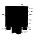
在图7中,是为用熟知方法制作的n沟道晶体管的开关晶体管4502,被提供在衬底4501上。本说明书中的晶体管具有双栅结构。但也可以采用单栅结构、三栅结构、或具有3个以上栅的多栅结构。开关晶体管4502可以是用熟知方法制作的p沟道晶体管。In FIG. 7, a
驱动晶体管4503是用熟知方法制作的n沟道晶体管。开关晶体管4502的漏布线4504通过布线(图中未示出)被电连接到驱动晶体管4503的栅电极4506。The
驱动晶体管4503是一种用来控制发光元件4510中流动的电流量的元件,而大量电流流过驱动晶体管,从而增大了热或热载流子引起其退化的危险。因此,在驱动晶体管4503的漏区中,或在漏区和其源区的每个中提供LDD区,以便与栅电极重叠以栅绝缘膜夹于其间,是非常有效的。图7作为例子示出了LDD区被形成在各个驱动晶体管4503的源区和漏区中的情况。The
本实施方案中的驱动晶体管4503具有单栅结构,但也可以采用多栅结构,其中多个晶体管被串联连接。可以采用另一种结构,其中多个晶体管被并联连接,且基本上将一个沟道形成区分割成多个区域以便高效率地散热。作为对抗热引起的退化的措施,此结构是有效的。The driving
包括驱动晶体管4503的栅电极4506的布线(图中未示出),与驱动晶体管4503的漏布线4512部分地重叠之间夹以绝缘膜。电容存储器被制作在这一重叠区域中。电容存储器具有保持施加到驱动晶体管4503的栅电极4506的电压的功能。A wiring (not shown) including a
第一层间绝缘膜4514被制作在开关晶体管4502和驱动晶体管4503上。在第一层间绝缘膜上。由树脂绝缘膜形成第二层间绝缘膜4515。A first
4517表示的是由高度透明的导电膜形成的象素电极(发光元件的阳极)。象素电极被制作成部分覆盖驱动晶体管4503的漏区,并被电连接到其上。象素电极4517可以由氧化铟与氧化锡的化合物(称为ITO)或氧化铟与氧化锌的化合物组成。其它透明导电膜当然也可以用来形成象素电极4517。4517 denotes a pixel electrode (anode of a light-emitting element) formed of a highly transparent conductive film. The pixel electrode is formed to partially cover the drain region of the driving
接着,在象素电极4517上形成有机树脂膜4516,并对面向象素电极4517的膜部分进行图形化以形成有机化合物层4519。虽然在图7中未示出,但可以分别形成发红光的R有机化合物层4519、发绿光的G有机化合物层4519、以及发蓝光的B有机化合物层4519。有机化合物层4519的发光材料是一种π共轭聚合物基材料。聚合物基材料的典型例子包括聚对位亚苯基乙烯(PPV)基材料、聚乙烯咔唑(PVK)基材料、以及聚芴基材料。在本发明中,有机化合物层4519可以是单层结构或多层结构。可以自由地组合熟知的材料和结构以形成有机化合物层4519(用来发光、移动载流子、以及注入载流子的层)。Next, an
例如,虽然本实施方案示出了聚合物基材料被用于有机化合物层4519的离子,但也可以采用低分子量有机发光材料。也可以用碳化硅或其它无机材料作为电荷输运层和电荷注入层。这些有机发光材料和无机材料可以是熟知的材料。For example, although the present embodiment shows that a polymer-based material is used for the ions of the
当制作阴极4523时,就完成了发光元件4510。此处,发光元件4510指的是由象素电极4517、有机化合物层4519、空穴注入层4522、以及阴极4523组成的叠层。When the
在本实施方案中,钝化膜4524被制作在阴极4523上。最好用氮化硅膜或氮氧化硅膜作为钝化膜4524。这是为了使发光元件4510隔绝于外界并防止发光材料氧化造成的退化和降低来自发光材料的气体泄漏。从而提高了发光器件的可靠性。In this embodiment, a
在本实施方案中,如上所述的发光器件具有象素结构如图7所示的象素部分,并具有关断电流值足够低的选择晶体管和能够承受热载流子注入的驱动晶体管。因此,能够获得高度可靠并能显示优异图象的发光器件。In this embodiment, the light emitting device as described above has a pixel portion having a pixel structure as shown in FIG. 7, and has a selection transistor having a sufficiently low off current value and a driving transistor capable of withstanding hot carrier injection. Therefore, a highly reliable light-emitting device capable of displaying excellent images can be obtained.
在具有本实施方案所述结构的发光器件中,有机化合物层4519中产生的光,如箭头所示向着其上制作晶体管的衬底4501的方向发射。光从发光元件4510向着衬底4501的方向发射,被称为向下发射。In the light emitting device having the structure described in this embodiment, light generated in the
接着,参照图17A和17B来描述发光器件的剖面结构,其中光从发光元件向着背向衬底的方向发射(向上发射)。Next, a cross-sectional structure of a light emitting device in which light is emitted from the light emitting element toward the direction away from the substrate (upward emission) will be described with reference to FIGS. 17A and 17B .
在图17A中,驱动晶体管1601被制作在衬底1600上。驱动晶体管1601具有源区1604a、漏区1604c、以及沟道形成区1604b。驱动晶体管还在沟道形成区1604b上方具有栅电极1603a,以栅绝缘膜1605插入其间。熟知的结构能够被自由地用于驱动晶体管1601而不局限于图17A所示的结构。In FIG. 17A , a
层间膜1606被制作在驱动晶体管1601上。接着,形成I TO膜或其它透明导电膜,并图形化成所需形状以获得象素电极1608。此处的象素电极1608用作发光元件1614的阳极。An
在层间膜1606中制作达及驱动晶体管1601的源区1604a和漏区1604c的接触孔。然后制作由Ti层、含Ti的Al层、以及另一Ti层组成的叠层,并图形化成所需的形状。这样得到的是布线1607和1609。Contact holes reaching the
随后,制作由丙烯酸或其它有机树脂材料组成的绝缘膜。在绝缘膜中与发光元件1614象素电极1608的位置重合的位置处制作窗口,以获得绝缘膜1610。窗口的侧壁必须足够平缓,以避免有机化合物层由于窗口侧壁的高程差而退化和连接断开等。Subsequently, an insulating film composed of acrylic or other organic resin material is formed. A window is formed in the insulating film at a position that coincides with the position of the
制作有机化合物层1611,然后由叠层形成发光元件1614的反电极(阴极)1612。此叠层具有厚度为2nm或更小的铯(Cs)膜和其上厚度为10nm或更小的银(Ag)膜。借助于形成发光元件1614的非常薄的反电极1612,从有机化合物层1611发射的光通过反电极1612透射,并沿与衬底1600相反的方向射出。为了保护发光元件1614,制作保护膜1613。An
图17B是不同于图17A的结构的剖面图。在图17B中,与图17A完全相同的元件用相同的参考号表示。直至形成图17B结构的驱动晶体管1601和层间膜1606的各个步骤,与结构17A的步骤相同。其解释因而从略。Fig. 17B is a cross-sectional view of a structure different from Fig. 17A. In FIG. 17B, elements identical to those in FIG. 17A are denoted by the same reference numerals. The steps up to forming the driving
在层间膜1606中制作达及驱动晶体管1601的源区1604a和漏区1604c的接触孔。然后制作由Ti层、含Ti的Al层、以及另一Ti层组成的叠层。随后,制作透明导电膜,典型为ITO膜。由Ti层、含Ti的Al层、以及另一Ti层组成的叠层以及典型为ITO膜的透明导电膜,被图形化成所需的形状,以便得到布线1607、1608和1609以及象素电极1620。象素电极1620用作发光元件1624的阳极。Contact holes reaching the
随后,由丙烯酸或其它有机树脂材料形成绝缘膜。在绝缘膜中与发光元件1624象素电极1620的位置重合的位置处制作窗口,以获得绝缘膜1610。窗口的侧壁必须足够平缓,以避免有机化合物层由于窗口侧壁的高程差而退化和连接断开等。Subsequently, an insulating film is formed of acrylic or other organic resin material. A window is formed in the insulating film at a position that coincides with the position of the
制作有机化合物层1611,然后由叠层形成发光元件1624的反电极(阴极)1612。此叠层具有厚度为2nm或更小的铯(Cs)膜和其上厚度为10nm或更小的银(Ag)膜。借助于形成发光元件1624的非常薄的反电极1612,从有机化合物层1611发射的光通过反电极1612透射,并沿与衬底1600相反的方向射出。为了保护发光元件1624,随后制作保护膜1613。An
如上所述,由于从发光元件1614发射的光不必通过制作在衬底1600上的驱动晶体管1601和其它元件来观察,故沿与衬底1600相反的方向发光的发光器件能够具有更大的窗口比。As described above, since the light emitted from the
如图17B所示构成的象素能够使用同一个光掩模来图形化连接到驱动晶体管源区或漏区的布线1619和图形化象素电极1620。因此,比之如图17A所示构成的象素,减少了制造工艺中所需的光掩模的数量并简化了工艺。A pixel constructed as shown in FIG. 17B can use the same photomask to pattern the
本实施方案可以与实施方案模式和实施方案1自由地组合。This embodiment can be freely combined with Embodiment Mode and
实施方案3Embodiment 3
在本实施方案中,参照图8A和8B来描述发光器件的外貌。In this embodiment, the appearance of the light emitting device is described with reference to FIGS. 8A and 8B.
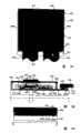
图8A是发光器件的俯视图,图8B是沿图8A中A-A’线的剖面图,而图8C是沿图8A中B-B’线的剖面图。8A is a top view of a light emitting device, FIG. 8B is a cross-sectional view along line A-A' in FIG. 8A, and FIG. 8C is a cross-sectional view along line B-B' in FIG. 8A.
密封元件4009被提供成环绕制作在衬底4001上的象素部分4002、源信号线驱动电路4003、以及第一和第二栅信号线驱动电路4004a和4004b。而且,密封材料4008被提供在象素部分4002、源信号线驱动电路4003、以及第一和第二栅信号线驱动电路4004a和4004b上。象素部分4002、源信号线驱动电路4003、以及第一和第二栅信号线驱动电路4004a和4004b,被衬底4001、密封元件4009、以及密封材料4008与填充剂4210一起密封。A sealing
顺便说一下,在本实施方案中,一对(二个)栅信号线驱动电路被制作在衬底上。但本发明不局限于此,栅信号线驱动电路和源信号线驱动电路的数目由设计者随意提供。Incidentally, in this embodiment, a pair (two) of gate signal line driver circuits are formed on a substrate. However, the present invention is not limited thereto, and the number of gate signal line driving circuits and source signal line driving circuits can be freely provided by the designer.
而且,提供在衬底4001上的象素部分4002、源信号线驱动电路4003、以及第一和第二栅信号线驱动电路4004a和4004b,具有多个晶体管。在图8B中,典型地示出了制作在基底膜4010上的包括在源信号线驱动电路4003中的驱动电路晶体管(但此处示出了n沟道晶体管和p沟道晶体管)4201以及包括在象素部分4002中的驱动晶体管(控制流到发光元件的电流的晶体管)4202。Also, the
在本实施方案中,用熟知方法制作的p沟道晶体管或n沟道晶体管,被用作驱动电路晶体管4201,而用熟知方法制作的p沟道晶体管,被用作驱动晶体管4202。而且,象素部分4002配备有连接到驱动晶体管4202栅电极的存储电容器(未示出)。In this embodiment, a p-channel transistor or an n-channel transistor fabricated by a known method is used as the
层间绝缘膜(整平膜)4301被制作在驱动电路晶体管4201和驱动晶体管4202上,并在其上制作电连接到驱动晶体管4202的漏的象素电极(阳极)4203。功函数大的透明导电膜被用于象素电极4203。氧化铟与氧化锡的化合物、氧化铟与氧化锌的化合物、氧化锌、氧化锡、或氧化铟,可以被用于透明导电膜。也可以使用掺镓的上述透明导电膜。An interlayer insulating film (leveling film) 4301 is formed on the
然后,绝缘膜4302被制作在象素电极4203上,且绝缘膜4302在象素电极4203上被制作成具有窗口部分。在此窗口部分中,在象素电极4203上形成有机化合物层4204。熟知的有机发光材料或无机发光材料可以被用于有机化合物层4204。而且作为有机发光材料,存在着低分子量(单体)材料和高分子量(聚合物)材料,二种材料都可以使用。Then, an insulating
熟知的蒸发技术或涂敷技术可以被用作形成有机化合物层4204的方法。而且,有机化合物层的结构可以借助于自由组合空穴注入层、空穴输运层、发光层、电子输运层、以及电子注入层而取叠层结构或单层结构。A well-known evaporation technique or coating technique can be used as a method of forming the
由具有遮光性质的导电膜(典型为含铝、铜、或银作为其主要成分的导电膜,或上述导电膜与其它导电膜的叠层膜)组成的阴极4205,被制作在有机化合物层4204上。而且,希望尽可能多地清除存在于阴极4205与有机化合物层4204之间界面上的潮气和氧。因此,这种器件必须在氮气或稀有气体气氛中制作有机化合物层4204,然后制作阴极4205而不暴露于氧和潮气。在本实施方案中,利用多工作室型(组合工具型)制膜装置实现了上述的膜淀积。此外,预定的电压被施加到阴极4205。A
如上所述,制作了由象素电极(阳极)4203、有机化合物层4204、以及阴极4205组成的发光元件4303。而且,保护膜4209被制作在绝缘膜4302上,以便覆盖发光元件4303。在防止氧和潮气等渗透发光元件4303方面,保护膜4209是有效的。As described above, the light-emitting
参考号4005a表示延伸连接到电源线的布线,且布线4005a被电连接到驱动晶体管4202的源区。延伸布线4005a通过密封元件4009与衬底4001之间,并通过各向异性导电膜4300被电连接到FPC 4006的FPC布线4301。
玻璃材料、金属材料(典型为不锈钢材料)、陶瓷材料、或塑料材料(包括塑料膜),能够被用于密封材料4008。FRP(玻璃纤维加固的塑料)板、PVF(聚氟乙烯)膜、Mylar膜、聚酯膜、或丙烯酸树脂膜,可以被用作塑料材料。而且,也可以使用具有铝箔被PVF膜或Mylar膜夹在中间的结构的片。A glass material, a metal material (typically a stainless steel material), a ceramic material, or a plastic material (including a plastic film), can be used for the sealing
但在发光元件的光向着覆盖元件侧发射的情况下,覆盖元件必须透明。在此情况下,采用诸如玻璃片、塑料片、聚酯膜、或丙烯酸膜之类的透明衬底。However, in the case where the light of the light-emitting element is emitted towards the side of the covering element, the covering element must be transparent. In this case, a transparent substrate such as a glass sheet, plastic sheet, polyester film, or acrylic film is used.
而且,除了氮气或氩气之类的惰性气体外,可紫外线固化的树脂或热塑树脂可以被用作填充剂4103,致使能够使用PVC(聚氯乙烯)、丙烯酸、聚酰亚胺、环氧树脂、硅酮树脂、PVB(聚丁缩醛乙烯)、或EVA(聚乙烯醋酸乙烯)。在本实施方案中,氮气被用作填充剂。Also, in addition to inert gas such as nitrogen or argon, ultraviolet curable resin or thermoplastic resin can be used as the filler 4103, enabling the use of PVC (polyvinyl chloride), acrylic, polyimide, epoxy resin, silicone resin, PVB (polyvinyl butyral), or EVA (polyvinyl acetate). In this embodiment, nitrogen gas is used as a filler.
而且,在衬底4001侧上的密封材料4008的表面上提供凹陷部分4007,吸湿性物质或能够吸收氧的物质4207被安置在其中,以便填充剂4103被暴露于吸湿性物质(最好是氧化钡)或能够吸收氧的物质。然后用凹陷部分覆盖元件4208将吸湿性物质或能够吸收氧的物质4207夹持在凹陷部分4007中,使吸湿性物质或能够吸收氧的物质4207不致分散。注意,凹陷部分覆盖元件4208具有细小网格形状,并具有空气和潮气可穿透而吸湿性物质或能够吸收氧的物质4207不穿透的结构。借助于提供吸湿性物质或能够吸收氧的物质4207,能够抑制发光元件4303的退化。Also, on the surface of the sealing
如图8C所示,制作象素电极4203,且同时制作导电膜4203a,以便接触延伸布线4005a。As shown in FIG. 8C, a
而且,各向异性导电膜4300具有导电填充剂4300a。借助于对衬底4001和FPC 4006进行热压,衬底4001上的导电膜4203a与FPC 4006上的FPC布线4301被导电填充剂4300a彼此电连接。Also, the anisotropic
本发明的发光器件的安培表和修正电路被制作在不同于衬底4001的衬底(未示出)上,并通过FPC 4006被电连接到制作在衬底4001上的电源线和阴极4205。The ammeter and correction circuit of the light-emitting device of the present invention are made on a substrate (not shown) different from the
注意,借助于与实施方案模式以及实施方案1和2进行自由组合,能够实现本实施方案。Note that this embodiment can be realized by free combination with Embodiment Mode and Embodiments 1 and 2.
实施方案4
在本实施方案中,参照图9,利用本发明来描述不同于实施方案3的发光器件的外貌。更具体地说,参照图9描述了一种发光器件的外貌,其中安培表和修正电路被制作在不同于其上制作象素部分的衬底的衬底上,并被诸如引线键合方法或COG(玻璃上芯片)方法之类的装置连接到其上制作象素部分的衬底上的布线。In this embodiment, referring to FIG. 9 , the appearance of a light emitting device different from Embodiment 3 is described using the present invention. More specifically, an appearance of a light emitting device is described with reference to FIG. A device such as a COG (Chip On Glass) method is connected to the wiring on the substrate on which the pixel portion is formed.
图9是本实施方案发光器件的外貌图。密封元件5009被提供成环绕提供在衬底5001上的象素部分5002、源信号线驱动电路5003、以及第一和第二栅信号线驱动电路5004a和5004b。而且,密封材料5008被提供在象素部分5002、源信号线驱动电路5003、以及第一和第二栅信号线驱动电路5004a和5004b上。于是,象素部分5002、源信号线驱动电路5003、以及第一和第二栅信号线驱动电路5004a和5004b,被衬底5001、密封元件5009、以及密封材料5008与填充剂(未示出)一起密封。Fig. 9 is an external view of the light emitting device of this embodiment. A sealing
注意,在本实施方案中,虽然二个栅信号线驱动电路被制作在衬底5001上,但本发明不局限于此。栅信号线驱动电路和源信号线驱动电路的数目由设计者随意提供。Note that, in this embodiment, although two gate signal line driver circuits are fabricated on the
在衬底5001侧上的密封材料5008的表面上提供凹陷部分5007,吸湿性物质或能够吸收氧的物质被安置在其中。A recessed
延伸到衬底5001的布线(延伸布线)通过密封元件5009与衬底5001之间,并通过FPC 5006被连接到发光器件的外部电路或元件。Wiring (extended wiring) extending to the
安培表和修正电路被制作在不同于衬底5001的衬底(以下称为芯片)5020上。用诸如COG(玻璃上芯片)方法之类的装置,芯片5020被固定到衬底5001,并被电连接到制作在衬底5001上的电源线和阴极(未示出)。The ammeter and correction circuit are fabricated on a substrate (hereinafter referred to as a chip) 5020 different from the
在本实施方案中,利用引线键合方法和COG方法等,其上制作安培表、可变电源、以及修正电路的芯片5020被固定到衬底5001。能够基于一个衬底来构成发光器件,因此,器件本身被做得紧凑并改善了机械强度。In the present embodiment, a
注意,关于将芯片连接到衬底上的方法,可以采用熟知的方法。而且,安培表和修正电路之外的电路和元件可以被固定到衬底5001上。Note that, as a method of connecting a chip to a substrate, a well-known method can be employed. Also, circuits and components other than the ammeter and correction circuit may be fixed to the
借助于与实施方案模式以及实施方案1-3进行自由组合,能够实现本实施方案。This embodiment can be realized by free combination with the embodiment mode and embodiments 1-3.
实施方案5Embodiment 5
发光器件是自发光的,因而在明亮环境中的清晰度优越于液晶显示器件,并具有更广阔的视角。因此,本发明的发光器件能够被应用于各种电子设备的显示单元。The light-emitting device is self-luminous, so the clarity in bright environments is superior to that of liquid crystal display devices, and it has a wider viewing angle. Therefore, the light emitting device of the present invention can be applied to display units of various electronic devices.
采用本发明的发光器件的电器的例子是:摄象机;数码相机;风镜式显示器(头戴显示器);导航系统;声音重放装置(车辆音响、音响元件等);膝上计算机;游戏机;便携式信息终端(移动计算机、蜂窝电话、便携式游戏机、电子记事本等);包括记录媒质的图象重放装置(具体地说是能够处理诸如数字万能视盘(DVD)之类的记录媒质中的数据,并具有能够显示数据图象的显示器件的电器)。特别是对于便携式信息终端,由于常常被倾斜地观察而要求宽广的视角,具有发光元件的发光器件是可取的。图10A-10H示出了这种电子装置的具体例子。Examples of electrical appliances employing the light-emitting device of the present invention are: video cameras; digital cameras; goggle displays (head-mounted displays); navigation systems; sound playback devices (vehicle audio, audio components, etc.); laptop computers; game machines ; portable information terminals (mobile computers, cellular phones, portable game machines, electronic notepads, etc.); image playback devices including recording media (specifically, devices capable of processing recording media such as digital versatile video discs (DVD) data and has a display device capable of displaying images of the data). Especially for portable information terminals, which require a wide viewing angle since they are often viewed obliquely, a light emitting device having a light emitting element is desirable. Specific examples of such electronic devices are shown in Figures 10A-10H.
图10A示出了发光器件,它包含机箱3001、支座3002、显示单元3003、扬声器单元3004、视频输入端子3005等。采用了本发明的发光器件,能够被用于显示单元3003。本发明的发光器件是自发光的,不需要后照光,致使能够制作比液晶显示器件更薄的显示单元。术语显示器件包括用来显示信息的各种显示器件,例如个人计算机的显示器件、接收电视广播的显示器件、以及广告显示器件。FIG. 10A shows a light emitting device, which includes a chassis 3001, a stand 3002, a display unit 3003, a speaker unit 3004, a video input terminal 3005, and the like. The light emitting device employing the present invention can be used in the display unit 3003 . The light-emitting device of the present invention is self-luminous and does not require backlighting, so that a display unit thinner than a liquid crystal display device can be manufactured. The term display device includes various display devices for displaying information, such as a display device for a personal computer, a display device for receiving television broadcasts, and an advertisement display device.
图10B示出了数码静物相机,它包含主体3101、显示单元3102、图象接收单元3103、操作键3104、外部连接端口3105、快门3106等。将本发明的发光器件用于显示单元3102,制作了数码静物相机。FIG. 10B shows a digital still camera, which includes a main body 3101, a display unit 3102, an image receiving unit 3103, operation keys 3104, an external connection port 3105, a shutter 3106, and the like. Using the light-emitting device of the present invention for the display unit 3102, a digital still camera was fabricated.
图10C示出了膝上计算机,它包含主体3201、机箱3202、显示单元3203、键盘3204、外部连接端口3205、定位鼠标3206等。将本发明的发光器件用于显示单元3203,制作了膝上计算机。FIG. 10C shows a laptop computer, which includes a main body 3201, a chassis 3202, a display unit 3203, a keyboard 3204, an external connection port 3205, a pointing mouse 3206, and the like. A laptop computer was produced by using the light-emitting device of the present invention for the display unit 3203 .
图10D示出了移动计算机,它包括主体3301、显示单元3302、开关3303、操作键3304、红外端口3305等。将本发明的发光器件用于显示单元3302,制作了移动计算机。FIG. 10D shows a mobile computer, which includes a main body 3301, a display unit 3302, a switch 3303, operation keys 3304, an infrared port 3305, and the like. A mobile computer was produced by using the light-emitting device of the present invention in the display unit 3302 .
图10E示出了配备有记录媒质的便携式图象重放装置(具体地说是DVD碟机),此装置包含主体3401、机箱3402、显示单元A 3403、显示单元B 3404、记录媒质(例如DVD)读出单元3405、操作键3406、扬声器单元3407等。显示单元A 3403主要显示图象信息,而显示单元B 3404主要显示文本信息。将本发明的发光器件用于显示单元A3403和B 3404,制作了便携式图象重放装置。术语配备有记录媒质的图象重放装置包括家用游戏机。Figure 10E shows a portable image playback device equipped with a recording medium (specifically, a DVD player), which includes a main body 3401, a chassis 3402, a display unit A 3403, a display unit B 3404, a recording medium (such as a DVD ) readout unit 3405, operation keys 3406, speaker unit 3407, and the like. The display unit A 3403 mainly displays image information, and the display unit B 3404 mainly displays text information. The light-emitting device of the present invention was used in the display units A3403 and B3404 to manufacture a portable image playback device. The term image playback apparatus equipped with a recording medium includes home game machines.
图10F示出了风镜式显示器(头戴显示器),它包含主体3501、显示单元3502、以及镜臂单元3503。将本发明的发光器件用于显示单元3502,制作了风镜式显示器。FIG. 10F shows a goggle display (head-mounted display), which includes a main body 3501 , a display unit 3502 , and a mirror arm unit 3503 . The light-emitting device of the present invention was used in the display unit 3502 to manufacture a goggle display.
图10G示出了摄象机,它包含主体3601、显示单元3602、机箱3603、外部连接端口3604、遥控接收单元3605、图象接收单元3606、电池3607、声音输入单元3608、操作键3609等。将本发明的发光器件用于显示单元3602,制作了摄象机。10G shows a video camera, which includes a
图10H示出了蜂窝电话,它包含主体3701、机箱3702、显示单元3703、声音输入单元3704、声音输出单元3705、操作键3706、外部连接端口3707、天线3708等。将本发明的发光器件用于显示单元3703,制作了蜂窝电话。若显示单元3703在黑色背景上显示白色字符,则能够降低蜂窝电话的功耗。10H shows a cellular phone, which includes a main body 3701, a housing 3702, a display unit 3703, a voice input unit 3704, a voice output unit 3705, operation keys 3706, an external connection port 3707, an antenna 3708, and the like. Using the light-emitting device of the present invention for the display unit 3703, a cellular phone was produced. If the display unit 3703 displays white characters on a black background, the power consumption of the cellular phone can be reduced.
如果有机材料发射的光的亮度将来得到了提高,则本发明的发光器件还能够被用于正投型或背投型投影仪,其中携带被输出的图象信息的光被透镜等放大投射到屏幕上。If the brightness of the light emitted by the organic material is improved in the future, the light-emitting device of the present invention can also be used in a front-projection or rear-projection projector, wherein the light carrying the output image information is enlarged and projected onto the on the screen.
上述电子装置经常显示通过诸如互连网和CATV(有线电视)之类的电子通信线路传播的信息,特别是频率越来越高的动画信息。本发明的发光器件由于有机材料具有快速的响应速度而适合于显示动画。The above-mentioned electronic devices often display information transmitted through electronic communication lines such as the Internet and CATV (Cable TV), especially animation information with increasing frequency. The light emitting device of the present invention is suitable for displaying animation due to the fast response speed of the organic material.
在发光器件中,发光的部分消耗功率。因此,希望以尽可能小部分的发光来显示信息。因此,若发光器件被用于诸如便携式信息终端特别是蜂窝电话以及声音重放装置之类的主要显示文本信息的显示单元,则希望指定发光部分来显示文本信息,而不发光部分用作背景。In a light emitting device, the part that emits light consumes power. Therefore, it is desirable to display information with as little light emission as possible. Therefore, if the light emitting device is used in a display unit mainly displaying text information such as a portable information terminal, especially a cellular phone, and a sound playback device, it is desirable to designate a light emitting portion to display text information, and a non-light emitting portion to be used as a background.
如上所述,采用本发明的发光器件的应用范围非常广阔,各种领域的电器都能够采用此器件。As mentioned above, the application range of the light emitting device of the present invention is very wide, and electrical appliances in various fields can use this device.
本发明计算适合于各个象素的驱动晶体管特性的视频信号而不改变象素的结构。得到的视频信号被输入到象素,以便使电流以所希望的量在发光元件中流动,从而能够得到所需的发光。结果,提供了一种发光器件及其驱动方法,其中消除了用来控制发光元件的晶体管之间特性起伏的影响。The present invention calculates a video signal suitable for the characteristics of the driving transistor of each pixel without changing the structure of the pixel. The obtained video signal is input to the pixel so that a desired amount of current flows through the light emitting element so that desired light emission can be obtained. As a result, there are provided a light emitting device and a driving method thereof in which influence of fluctuation in characteristics between transistors used to control a light emitting element is eliminated.
如上所述构成的本发明能够提供发光器件及其驱动方法,其中用模拟方法来驱动发光器件,并消除了晶体管之间特性起伏的影响,从而得到了清晰的多灰度显示。而且,本发明能够提供发光器件及其驱动方法,其中减小了发光元件二个电极之间流动的电流量随老化的变化,从而得到了清晰的多灰度显示。The present invention constituted as described above can provide a light emitting device and a driving method thereof in which the light emitting device is driven by an analog method and the influence of fluctuations in characteristics between transistors is eliminated, thereby obtaining a clear multi-gradation display. Furthermore, the present invention can provide a light emitting device and a driving method thereof, in which the variation with aging of the amount of current flowing between two electrodes of the light emitting element is reduced, thereby obtaining a clear multi-gray scale display.
Claims (57)
Applications Claiming Priority (3)
| Application Number | Priority Date | Filing Date | Title |
|---|---|---|---|
| JP271424/01 | 2001-09-07 | ||
| JP2001271424 | 2001-09-07 | ||
| JP271424/2001 | 2001-09-07 |
Related Child Applications (1)
| Application Number | Title | Priority Date | Filing Date |
|---|---|---|---|
| CNA2008101843042ADivisionCN101425260A (en) | 2001-09-07 | 2002-09-06 | Luminous device and its driving method |
Publications (2)
| Publication Number | Publication Date |
|---|---|
| CN1407526A CN1407526A (en) | 2003-04-02 |
| CN100454375Ctrue CN100454375C (en) | 2009-01-21 |
Family
ID=19096934
Family Applications (2)
| Application Number | Title | Priority Date | Filing Date |
|---|---|---|---|
| CNB021318220AExpired - Fee RelatedCN100454375C (en) | 2001-09-07 | 2002-09-06 | Light emitting device and driving method thereof |
| CNA2008101843042APendingCN101425260A (en) | 2001-09-07 | 2002-09-06 | Luminous device and its driving method |
Family Applications After (1)
| Application Number | Title | Priority Date | Filing Date |
|---|---|---|---|
| CNA2008101843042APendingCN101425260A (en) | 2001-09-07 | 2002-09-06 | Luminous device and its driving method |
Country Status (5)
| Country | Link |
|---|---|
| US (3) | US7088052B2 (en) |
| JP (8) | JP2009086673A (en) |
| KR (11) | KR100936044B1 (en) |
| CN (2) | CN100454375C (en) |
| TW (1) | TWI221268B (en) |
Families Citing this family (148)
| Publication number | Priority date | Publication date | Assignee | Title |
|---|---|---|---|---|
| TWI221268B (en)* | 2001-09-07 | 2004-09-21 | Semiconductor Energy Lab | Light emitting device and method of driving the same |
| US7170478B2 (en)* | 2002-03-26 | 2007-01-30 | Semiconductor Energy Laboratory Co., Ltd. | Method of driving light-emitting device |
| US6911781B2 (en) | 2002-04-23 | 2005-06-28 | Semiconductor Energy Laboratory Co., Ltd. | Light emitting device and production system of the same |
| US7180513B2 (en) | 2002-04-26 | 2007-02-20 | Toshiba Matsushita Display Technology Co., Ltd. | Semiconductor circuits for driving current-driven display and display |
| EP1624435A1 (en)* | 2003-05-07 | 2006-02-08 | Toshiba Matsushita Display Technology Co., Ltd. | El display and its driving method |
| KR100934293B1 (en) | 2003-05-07 | 2009-12-29 | 도시바 모바일 디스플레이 가부시키가이샤 | Matrix display device |
| JP4838498B2 (en)* | 2003-05-21 | 2011-12-14 | キヤノン株式会社 | Display device |
| JP2005099713A (en)* | 2003-08-25 | 2005-04-14 | Seiko Epson Corp | Electro-optical device, driving method of electro-optical device, and electronic apparatus |
| JP2005084260A (en)* | 2003-09-05 | 2005-03-31 | Agilent Technol Inc | Display panel conversion data determination method and measuring apparatus |
| CA2443206A1 (en) | 2003-09-23 | 2005-03-23 | Ignis Innovation Inc. | Amoled display backplanes - pixel driver circuits, array architecture, and external compensation |
| JP2005107059A (en)* | 2003-09-29 | 2005-04-21 | Sanyo Electric Co Ltd | Display device |
| JP4804711B2 (en)* | 2003-11-21 | 2011-11-02 | 株式会社 日立ディスプレイズ | Image display device |
| EP1818899A4 (en)* | 2003-12-02 | 2011-02-16 | Toshiba Matsushita Display Tec | Driving method of self-luminous type display unit, display control device of self-luminous type display unit, current output type drive circuit of self-luminous type display unit |
| JP4855648B2 (en) | 2004-03-30 | 2012-01-18 | グローバル・オーエルイーディー・テクノロジー・リミテッド・ライアビリティ・カンパニー | Organic EL display device |
| KR100580555B1 (en)* | 2004-03-31 | 2006-05-16 | 엘지.필립스 엘시디 주식회사 | Electro-luminescence display panel and its driving method |
| CA2472671A1 (en) | 2004-06-29 | 2005-12-29 | Ignis Innovation Inc. | Voltage-programming scheme for current-driven amoled displays |
| US8248392B2 (en)* | 2004-08-13 | 2012-08-21 | Semiconductor Energy Laboratory Co., Ltd. | Light emitting device using light emitting element and driving method of light emitting element, and lighting apparatus |
| US9734901B2 (en)* | 2004-10-29 | 2017-08-15 | Semiconductor Energy Laboratory Co., Ltd. | Display device with semiconductor memory cell |
| US20070035488A1 (en)* | 2004-12-03 | 2007-02-15 | Semiconductor Energy Laboratory Co., Ltd. | Driving method of display device |
| US20140111567A1 (en) | 2005-04-12 | 2014-04-24 | Ignis Innovation Inc. | System and method for compensation of non-uniformities in light emitting device displays |
| US8599191B2 (en) | 2011-05-20 | 2013-12-03 | Ignis Innovation Inc. | System and methods for extraction of threshold and mobility parameters in AMOLED displays |
| US9171500B2 (en) | 2011-05-20 | 2015-10-27 | Ignis Innovation Inc. | System and methods for extraction of parasitic parameters in AMOLED displays |
| US9275579B2 (en) | 2004-12-15 | 2016-03-01 | Ignis Innovation Inc. | System and methods for extraction of threshold and mobility parameters in AMOLED displays |
| US10013907B2 (en) | 2004-12-15 | 2018-07-03 | Ignis Innovation Inc. | Method and system for programming, calibrating and/or compensating, and driving an LED display |
| US8576217B2 (en) | 2011-05-20 | 2013-11-05 | Ignis Innovation Inc. | System and methods for extraction of threshold and mobility parameters in AMOLED displays |
| US9280933B2 (en) | 2004-12-15 | 2016-03-08 | Ignis Innovation Inc. | System and methods for extraction of threshold and mobility parameters in AMOLED displays |
| US9799246B2 (en) | 2011-05-20 | 2017-10-24 | Ignis Innovation Inc. | System and methods for extraction of threshold and mobility parameters in AMOLED displays |
| US10012678B2 (en) | 2004-12-15 | 2018-07-03 | Ignis Innovation Inc. | Method and system for programming, calibrating and/or compensating, and driving an LED display |
| TWI402790B (en) | 2004-12-15 | 2013-07-21 | Ignis Innovation Inc | Method and system for programming, calibrating and driving a light-emitting element display |
| US20060158399A1 (en)* | 2005-01-14 | 2006-07-20 | Semiconductor Energy Laboratory Co., Ltd. | Driving method of display device |
| CA2496642A1 (en) | 2005-02-10 | 2006-08-10 | Ignis Innovation Inc. | Fast settling time driving method for organic light-emitting diode (oled) displays based on current programming |
| US7595778B2 (en) | 2005-04-15 | 2009-09-29 | Semiconductor Energy Laboratory Co., Ltd. | Display device and electronic device using the same |
| US8044880B2 (en)* | 2005-04-28 | 2011-10-25 | Hitachi, Ltd. | Projection type image display device |
| US7598935B2 (en)* | 2005-05-17 | 2009-10-06 | Lg Electronics Inc. | Light emitting device with cross-talk preventing circuit and method of driving the same |
| JP5355080B2 (en) | 2005-06-08 | 2013-11-27 | イグニス・イノベイション・インコーポレーテッド | Method and system for driving a light emitting device display |
| US9318053B2 (en)* | 2005-07-04 | 2016-04-19 | Semiconductor Energy Laboratory Co., Ltd. | Semiconductor device and driving method thereof |
| US7986287B2 (en) | 2005-08-26 | 2011-07-26 | Semiconductor Energy Laboratory Co., Ltd. | Display device and method of driving the same |
| CA2518276A1 (en) | 2005-09-13 | 2007-03-13 | Ignis Innovation Inc. | Compensation technique for luminance degradation in electro-luminance devices |
| JP2007086347A (en)* | 2005-09-21 | 2007-04-05 | Eastman Kodak Co | Display device |
| US7450094B2 (en)* | 2005-09-27 | 2008-11-11 | Lg Display Co., Ltd. | Light emitting device and method of driving the same |
| KR100757563B1 (en)* | 2005-11-15 | 2007-09-10 | 엘지전자 주식회사 | Cross-talk prevention organic electroluminescent device and method of driving same |
| JP5397935B2 (en)* | 2005-10-25 | 2014-01-22 | リクアビスタ ビー ヴィ | Reset circuit for display element |
| US8207914B2 (en)* | 2005-11-07 | 2012-06-26 | Global Oled Technology Llc | OLED display with aging compensation |
| TWM290262U (en)* | 2005-11-21 | 2006-05-01 | Hannspree Inc | Working device for assembling flat TV |
| EP1793366A3 (en) | 2005-12-02 | 2009-11-04 | Semiconductor Energy Laboratory Co., Ltd. | Semiconductor device, display device, and electronic device |
| JP5130634B2 (en)* | 2006-03-08 | 2013-01-30 | ソニー株式会社 | Self-luminous display device, electronic device, burn-in correction device, and program |
| TW200746022A (en) | 2006-04-19 | 2007-12-16 | Ignis Innovation Inc | Stable driving scheme for active matrix displays |
| JP4208902B2 (en)* | 2006-06-30 | 2009-01-14 | キヤノン株式会社 | Active matrix display device and driving method thereof |
| KR20080010796A (en)* | 2006-07-28 | 2008-01-31 | 삼성전자주식회사 | OLED display and driving method thereof |
| CA2556961A1 (en) | 2006-08-15 | 2008-02-15 | Ignis Innovation Inc. | Oled compensation technique based on oled capacitance |
| JP2008046427A (en) | 2006-08-18 | 2008-02-28 | Sony Corp | Image display device |
| JP2008076757A (en)* | 2006-09-21 | 2008-04-03 | Sanyo Electric Co Ltd | Electroluminescence display device and display variation correction method for electroluminescence display device |
| US20080122759A1 (en)* | 2006-11-28 | 2008-05-29 | Levey Charles I | Active matrix display compensating method |
| KR101403397B1 (en)* | 2006-11-29 | 2014-06-03 | 엘지디스플레이 주식회사 | Organic electro luminescence display |
| KR100821046B1 (en)* | 2006-12-19 | 2008-04-08 | 삼성에스디아이 주식회사 | Pixel and organic light emitting display device using same |
| JP5095200B2 (en)* | 2006-12-22 | 2012-12-12 | オンセミコンダクター・トレーディング・リミテッド | Electroluminescence display device and display panel drive device |
| JP5317419B2 (en)* | 2007-03-07 | 2013-10-16 | 株式会社ジャパンディスプレイ | Organic EL display device |
| US20090109142A1 (en)* | 2007-03-29 | 2009-04-30 | Toshiba Matsushita Display Technology Co., Ltd. | El display device |
| KR100873707B1 (en) | 2007-07-27 | 2008-12-12 | 삼성모바일디스플레이주식회사 | Organic light emitting display device and driving method thereof |
| JP5086766B2 (en)* | 2007-10-18 | 2012-11-28 | グローバル・オーエルイーディー・テクノロジー・リミテッド・ライアビリティ・カンパニー | Display device |
| JP2009276671A (en)* | 2008-05-16 | 2009-11-26 | Canon Inc | Light-emitting device |
| KR100962916B1 (en)* | 2008-08-06 | 2010-06-10 | 삼성모바일디스플레이주식회사 | Driver IC and organic light emitting display device using the same |
| JP5107824B2 (en)* | 2008-08-18 | 2012-12-26 | 富士フイルム株式会社 | Display device and drive control method thereof |
| JP5157791B2 (en)* | 2008-09-29 | 2013-03-06 | カシオ計算機株式会社 | Display drive device, display device, and drive control method for display device |
| TWI475544B (en)* | 2008-10-24 | 2015-03-01 | Semiconductor Energy Lab | Display device |
| KR101509118B1 (en)* | 2008-10-27 | 2015-04-08 | 삼성디스플레이 주식회사 | OLED display, apparatus and method for generating correction information thereof |
| JP5239773B2 (en)* | 2008-11-17 | 2013-07-17 | ソニー株式会社 | Display device |
| KR20100058140A (en)* | 2008-11-24 | 2010-06-03 | 삼성모바일디스플레이주식회사 | Pixel and organic light emitting display device using the same |
| US8130182B2 (en)* | 2008-12-18 | 2012-03-06 | Global Oled Technology Llc | Digital-drive electroluminescent display with aging compensation |
| US8217928B2 (en)* | 2009-03-03 | 2012-07-10 | Global Oled Technology Llc | Electroluminescent subpixel compensated drive signal |
| US8194063B2 (en)* | 2009-03-04 | 2012-06-05 | Global Oled Technology Llc | Electroluminescent display compensated drive signal |
| JP2010266490A (en)* | 2009-05-12 | 2010-11-25 | Sony Corp | Display device |
| US9311859B2 (en) | 2009-11-30 | 2016-04-12 | Ignis Innovation Inc. | Resetting cycle for aging compensation in AMOLED displays |
| US10319307B2 (en) | 2009-06-16 | 2019-06-11 | Ignis Innovation Inc. | Display system with compensation techniques and/or shared level resources |
| CA2688870A1 (en) | 2009-11-30 | 2011-05-30 | Ignis Innovation Inc. | Methode and techniques for improving display uniformity |
| CA2669367A1 (en) | 2009-06-16 | 2010-12-16 | Ignis Innovation Inc | Compensation technique for color shift in displays |
| US9384698B2 (en) | 2009-11-30 | 2016-07-05 | Ignis Innovation Inc. | System and methods for aging compensation in AMOLED displays |
| JP5531496B2 (en)* | 2009-08-18 | 2014-06-25 | セイコーエプソン株式会社 | Image processing apparatus, display system, electronic apparatus, and image processing method |
| JP5471165B2 (en)* | 2009-08-26 | 2014-04-16 | セイコーエプソン株式会社 | Image processing apparatus, display system, electronic apparatus, and image processing method |
| US10996258B2 (en) | 2009-11-30 | 2021-05-04 | Ignis Innovation Inc. | Defect detection and correction of pixel circuits for AMOLED displays |
| US8803417B2 (en) | 2009-12-01 | 2014-08-12 | Ignis Innovation Inc. | High resolution pixel architecture |
| CA2686174A1 (en) | 2009-12-01 | 2011-06-01 | Ignis Innovation Inc | High reslution pixel architecture |
| CA2687631A1 (en) | 2009-12-06 | 2011-06-06 | Ignis Innovation Inc | Low power driving scheme for display applications |
| JP5146521B2 (en)* | 2009-12-28 | 2013-02-20 | カシオ計算機株式会社 | Pixel drive device, light emitting device, drive control method thereof, and electronic apparatus |
| JP5240581B2 (en)* | 2009-12-28 | 2013-07-17 | カシオ計算機株式会社 | Pixel drive device, light emitting device, drive control method thereof, and electronic apparatus |
| US10089921B2 (en) | 2010-02-04 | 2018-10-02 | Ignis Innovation Inc. | System and methods for extracting correlation curves for an organic light emitting device |
| US9881532B2 (en) | 2010-02-04 | 2018-01-30 | Ignis Innovation Inc. | System and method for extracting correlation curves for an organic light emitting device |
| US10163401B2 (en) | 2010-02-04 | 2018-12-25 | Ignis Innovation Inc. | System and methods for extracting correlation curves for an organic light emitting device |
| US20140313111A1 (en) | 2010-02-04 | 2014-10-23 | Ignis Innovation Inc. | System and methods for extracting correlation curves for an organic light emitting device |
| US10176736B2 (en) | 2010-02-04 | 2019-01-08 | Ignis Innovation Inc. | System and methods for extracting correlation curves for an organic light emitting device |
| CA2692097A1 (en) | 2010-02-04 | 2011-08-04 | Ignis Innovation Inc. | Extracting correlation curves for light emitting device |
| CA2696778A1 (en)* | 2010-03-17 | 2011-09-17 | Ignis Innovation Inc. | Lifetime, uniformity, parameter extraction methods |
| WO2011125109A1 (en)* | 2010-04-05 | 2011-10-13 | パナソニック株式会社 | Display method for an organic el display device, and organic el display device |
| KR101065405B1 (en)* | 2010-04-14 | 2011-09-16 | 삼성모바일디스플레이주식회사 | Display device and driving method |
| KR101322322B1 (en)* | 2010-09-22 | 2013-10-28 | 가시오게산키 가부시키가이샤 | Light emitting device and drive control method thereof, and electronic device |
| US8907991B2 (en) | 2010-12-02 | 2014-12-09 | Ignis Innovation Inc. | System and methods for thermal compensation in AMOLED displays |
| US9530349B2 (en) | 2011-05-20 | 2016-12-27 | Ignis Innovations Inc. | Charged-based compensation and parameter extraction in AMOLED displays |
| US9466240B2 (en) | 2011-05-26 | 2016-10-11 | Ignis Innovation Inc. | Adaptive feedback system for compensating for aging pixel areas with enhanced estimation speed |
| US9773439B2 (en) | 2011-05-27 | 2017-09-26 | Ignis Innovation Inc. | Systems and methods for aging compensation in AMOLED displays |
| US10089924B2 (en) | 2011-11-29 | 2018-10-02 | Ignis Innovation Inc. | Structural and low-frequency non-uniformity compensation |
| US9324268B2 (en) | 2013-03-15 | 2016-04-26 | Ignis Innovation Inc. | Amoled displays with multiple readout circuits |
| JP6012450B2 (en) | 2011-12-23 | 2016-10-25 | 株式会社半導体エネルギー研究所 | Driving method of semiconductor device |
| US8937632B2 (en) | 2012-02-03 | 2015-01-20 | Ignis Innovation Inc. | Driving system for active-matrix displays |
| KR101939231B1 (en)* | 2012-03-23 | 2019-01-17 | 엘지디스플레이 주식회사 | Organic light emitting diode display device and method of measuring pixel current of the same |
| US9747834B2 (en) | 2012-05-11 | 2017-08-29 | Ignis Innovation Inc. | Pixel circuits including feedback capacitors and reset capacitors, and display systems therefore |
| US8922544B2 (en) | 2012-05-23 | 2014-12-30 | Ignis Innovation Inc. | Display systems with compensation for line propagation delay |
| CN102881839B (en)* | 2012-09-28 | 2014-05-07 | 京东方科技集团股份有限公司 | Organic light emitting diode, touch display device and manufacture methods thereof |
| US9786223B2 (en) | 2012-12-11 | 2017-10-10 | Ignis Innovation Inc. | Pixel circuits for AMOLED displays |
| US9336717B2 (en) | 2012-12-11 | 2016-05-10 | Ignis Innovation Inc. | Pixel circuits for AMOLED displays |
| CN108665836B (en) | 2013-01-14 | 2021-09-03 | 伊格尼斯创新公司 | Method and system for compensating for deviations of a measured device current from a reference current |
| US9830857B2 (en) | 2013-01-14 | 2017-11-28 | Ignis Innovation Inc. | Cleaning common unwanted signals from pixel measurements in emissive displays |
| CN104919517B (en)* | 2013-01-21 | 2016-10-26 | 夏普株式会社 | Display device and data processing method of display device |
| EP3043338A1 (en) | 2013-03-14 | 2016-07-13 | Ignis Innovation Inc. | Re-interpolation with edge detection for extracting an aging pattern for amoled displays |
| WO2014174427A1 (en) | 2013-04-22 | 2014-10-30 | Ignis Innovation Inc. | Inspection system for oled display panels |
| KR102022696B1 (en) | 2013-04-30 | 2019-11-05 | 삼성디스플레이 주식회사 | Organic light emitting display device |
| CN105474296B (en) | 2013-08-12 | 2017-08-18 | 伊格尼斯创新公司 | A method and device for driving a display using image data |
| KR102083486B1 (en)* | 2013-10-04 | 2020-05-28 | 삼성디스플레이 주식회사 | Image sticking controller and method for operating the same |
| US9761170B2 (en) | 2013-12-06 | 2017-09-12 | Ignis Innovation Inc. | Correction for localized phenomena in an image array |
| US9741282B2 (en) | 2013-12-06 | 2017-08-22 | Ignis Innovation Inc. | OLED display system and method |
| US9502653B2 (en) | 2013-12-25 | 2016-11-22 | Ignis Innovation Inc. | Electrode contacts |
| DE102015206281A1 (en) | 2014-04-08 | 2015-10-08 | Ignis Innovation Inc. | Display system with shared level resources for portable devices |
| JP6653997B2 (en) | 2014-05-09 | 2020-02-26 | 株式会社半導体エネルギー研究所 | Display correction circuit and display device |
| US10074313B2 (en)* | 2014-06-10 | 2018-09-11 | Sharp Kabushiki Kaisha | Display device and method for driving same |
| KR20160008799A (en) | 2014-07-15 | 2016-01-25 | 김기봉 | Safe driving belt apparatus for baby carriage |
| US9797931B2 (en) | 2014-09-05 | 2017-10-24 | Semiconductor Energy Laboratory Co., Ltd. | Matrix device, measurement method of characteristics thereof, and driving method thereof |
| US10043427B2 (en) | 2014-09-05 | 2018-08-07 | Semiconductor Energy Laboratory Co., Ltd. | Matrix device, measurement method of characteristics thereof, and driving method thereof |
| US10170055B2 (en)* | 2014-09-26 | 2019-01-01 | Semiconductor Energy Laboratory Co., Ltd. | Display device and driving method thereof |
| WO2016046692A1 (en) | 2014-09-26 | 2016-03-31 | 株式会社半導体エネルギー研究所 | Matrix device, and drive method and properties measurement method for same |
| KR102226422B1 (en) | 2014-10-13 | 2021-03-12 | 삼성디스플레이 주식회사 | Orgainic light emitting display and driving method for the same |
| US9804719B2 (en) | 2014-10-23 | 2017-10-31 | Semiconductor Energy Laboratory Co., Ltd. | Electronic device |
| US10002564B2 (en) | 2014-10-31 | 2018-06-19 | Semiconductor Energy Laboratory Co., Ltd. | Display device, display module, and electronic device |
| JP6618779B2 (en)* | 2014-11-28 | 2019-12-11 | 株式会社半導体エネルギー研究所 | Semiconductor device |
| TWI682632B (en) | 2014-12-26 | 2020-01-11 | 日商半導體能源研究所股份有限公司 | Semiconductor device |
| CA2879462A1 (en) | 2015-01-23 | 2016-07-23 | Ignis Innovation Inc. | Compensation for color variation in emissive devices |
| JP2016177280A (en) | 2015-03-18 | 2016-10-06 | 株式会社半導体エネルギー研究所 | Display device, electronic device, and driving method of display device |
| JP2016206659A (en) | 2015-04-16 | 2016-12-08 | 株式会社半導体エネルギー研究所 | Display device, electronic device, and method for driving display device |
| US9496299B1 (en)* | 2015-05-01 | 2016-11-15 | Sensors Unlimited, Inc. | Layout for routing common signals to integrating imaging pixels |
| CA2889870A1 (en) | 2015-05-04 | 2016-11-04 | Ignis Innovation Inc. | Optical feedback system |
| CA2892714A1 (en) | 2015-05-27 | 2016-11-27 | Ignis Innovation Inc | Memory bandwidth reduction in compensation system |
| KR102457754B1 (en)* | 2015-08-04 | 2022-10-24 | 삼성디스플레이 주식회사 | Organic light emitting display device and method of driving the same |
| CA2900170A1 (en) | 2015-08-07 | 2017-02-07 | Gholamreza Chaji | Calibration of pixel based on improved reference values |
| KR102372041B1 (en)* | 2015-09-08 | 2022-03-11 | 삼성디스플레이 주식회사 | Display device and method of driving the same |
| US10007161B2 (en) | 2015-10-26 | 2018-06-26 | Semiconductor Energy Laboratory Co., Ltd. | Display device |
| CN108122534B (en)* | 2016-11-29 | 2019-03-26 | 昆山国显光电有限公司 | A kind of drive control circuit and its driving method, display device |
| KR20190125311A (en)* | 2017-03-07 | 2019-11-06 | 가부시키가이샤 한도오따이 에네루기 켄큐쇼 | ICs, driver ICs, display systems, and electronics |
| CN107068048B (en)* | 2017-06-06 | 2019-04-30 | 深圳市华星光电半导体显示技术有限公司 | Digital driving method of OLED display device |
| WO2019048966A1 (en) | 2017-09-05 | 2019-03-14 | 株式会社半導体エネルギー研究所 | Display system |
| WO2019053549A1 (en) | 2017-09-15 | 2019-03-21 | Semiconductor Energy Laboratory Co., Ltd. | Display device and electronic device |
Citations (11)
| Publication number | Priority date | Publication date | Assignee | Title |
|---|---|---|---|---|
| CN1086320A (en)* | 1992-10-30 | 1994-05-04 | 株式会社半导体能源研究所 | Matrix display and its driving method |
| WO1996024993A1 (en)* | 1995-02-10 | 1996-08-15 | National Semiconductor Corporation | Method and apparatus for transmitting data isochronously at a rate less than the isochronous data rate |
| CN1184579A (en)* | 1995-05-19 | 1998-06-10 | H·乔治·皮雷斯 | Video scrambling with variable function generator |
| CN1188299A (en)* | 1996-04-29 | 1998-07-22 | 国际商业机器公司 | TFT/LCD active data line repair |
| US5929872A (en)* | 1997-03-21 | 1999-07-27 | Alliance Semiconductor Corporation | Method and apparatus for multiple compositing of source data in a graphics display processor |
| JPH11298721A (en)* | 1998-04-06 | 1999-10-29 | Seiko Epson Corp | Image data interpolation apparatus, image data interpolation method, and medium recording image data interpolation program |
| JP2000076430A (en)* | 1998-08-28 | 2000-03-14 | Seiko Epson Corp | Image data interpolation device, image data interpolation method, and medium recording image data interpolation program |
| WO2000077533A2 (en)* | 1999-06-15 | 2000-12-21 | Seiko Epson Corporation | Semiconductor device simulation method and simulator |
| CN1290041A (en)* | 1999-09-24 | 2001-04-04 | 株式会社半导体能源研究所 | Electroluminescent displays and electronic devices |
| WO2001026085A1 (en)* | 1999-10-04 | 2001-04-12 | Matsushita Electric Industrial Co., Ltd. | Method of driving display panel, and display panel luminance correction device and display panel driving device |
| EP1128439A2 (en)* | 2000-02-28 | 2001-08-29 | Sel Semiconductor Energy Laboratory Co., Ltd. | Active matrix display device |
Family Cites Families (100)
| Publication number | Priority date | Publication date | Assignee | Title |
|---|---|---|---|---|
| JPH04285994A (en) | 1991-03-15 | 1992-10-12 | Matsushita Electron Corp | Liquid crystal display device, and manufacture and inspection thereof |
| US5245326A (en)* | 1991-08-19 | 1993-09-14 | International Business Machines Corp. | Calibration apparatus for brightness controls of digitally operated liquid crystal display system |
| JP2502871B2 (en)* | 1992-01-27 | 1996-05-29 | 松下電器産業株式会社 | LCD drive circuit and display device |
| CA2112431C (en)* | 1992-12-29 | 2000-05-09 | Masato Yamanobe | Electron source, and image-forming apparatus and method of driving the same |
| CA2138363C (en)* | 1993-12-22 | 1999-06-22 | Yasuyuki Todokoro | Electron beam generating apparatus, image display apparatus, and method of driving the apparatuses |
| CA2126535C (en)* | 1993-12-28 | 2000-12-19 | Ichiro Nomura | Electron beam apparatus and image-forming apparatus |
| JP3672586B2 (en) | 1994-03-24 | 2005-07-20 | 株式会社半導体エネルギー研究所 | Correction system and operation method thereof |
| JP3387617B2 (en)* | 1994-03-29 | 2003-03-17 | キヤノン株式会社 | Electron source |
| JP3311201B2 (en)* | 1994-06-08 | 2002-08-05 | キヤノン株式会社 | Image forming device |
| JP3251466B2 (en) | 1994-06-13 | 2002-01-28 | キヤノン株式会社 | Electron beam generator having a plurality of cold cathode elements, driving method thereof, and image forming apparatus using the same |
| JPH0982214A (en)* | 1994-12-05 | 1997-03-28 | Canon Inc | Electron emitting device, electron source, and image forming apparatus |
| JP3072251B2 (en) | 1995-04-28 | 2000-07-31 | リズム時計工業株式会社 | LED display device, display data creation method of LED display device, and writing controller |
| JP3219185B2 (en)* | 1995-08-23 | 2001-10-15 | キヤノン株式会社 | Electron generating device, image display device, their driving circuit, and driving method |
| JP3376220B2 (en)* | 1995-10-03 | 2003-02-10 | キヤノン株式会社 | Image forming apparatus and manufacturing method thereof |
| JPH09115673A (en) | 1995-10-13 | 1997-05-02 | Sony Corp | Light emission element or device, and driving method thereof |
| JPH09259753A (en)* | 1996-01-16 | 1997-10-03 | Canon Inc | Electron generating apparatus, image forming apparatus, and manufacturing method and adjusting method thereof |
| JPH09198007A (en) | 1996-01-16 | 1997-07-31 | Mitsubishi Electric Corp | Display device, brightness adjusting device, brightness adjusting method, and brightness adjusting system |
| US6621475B1 (en)* | 1996-02-23 | 2003-09-16 | Canon Kabushiki Kaisha | Electron generating apparatus, image forming apparatus, method of manufacturing the same and method of adjusting characteristics thereof |
| JP3618948B2 (en)* | 1996-03-11 | 2005-02-09 | キヤノン株式会社 | Image display device and driving method thereof |
| JP3106953B2 (en)* | 1996-05-16 | 2000-11-06 | 富士電機株式会社 | Display element driving method |
| JPH09318929A (en) | 1996-05-29 | 1997-12-12 | Toshiba Corp | Liquid crystal display device and display unevenness correction method |
| JPH1031449A (en) | 1996-07-12 | 1998-02-03 | Canon Inc | Display device, method for creating correction data for display device, and device therefor |
| CN100341042C (en)* | 1997-02-17 | 2007-10-03 | 精工爱普生株式会社 | Display device |
| US6518962B2 (en) | 1997-03-12 | 2003-02-11 | Seiko Epson Corporation | Pixel circuit display apparatus and electronic apparatus equipped with current driving type light-emitting device |
| JPH10254410A (en) | 1997-03-12 | 1998-09-25 | Pioneer Electron Corp | Organic electroluminescent display device, and driving method therefor |
| JPH1187053A (en) | 1997-09-04 | 1999-03-30 | Tdk Corp | Driving device for organic el display |
| JP3767877B2 (en)* | 1997-09-29 | 2006-04-19 | 三菱化学株式会社 | Active matrix light emitting diode pixel structure and method thereof |
| US6297791B1 (en) | 1997-11-21 | 2001-10-02 | Seiko Epson Corporation | Adjustment method of display device |
| JP3617344B2 (en) | 1997-11-21 | 2005-02-02 | セイコーエプソン株式会社 | Adjustment method of display device |
| JP3025249B2 (en)* | 1997-12-03 | 2000-03-27 | キヤノン株式会社 | Device driving device, device driving method, and image forming apparatus |
| JP3073486B2 (en)* | 1998-02-16 | 2000-08-07 | キヤノン株式会社 | Image forming apparatus, electron beam apparatus, modulation circuit, and driving method of image forming apparatus |
| JP3775628B2 (en)* | 1998-03-19 | 2006-05-17 | パイオニア株式会社 | Driving device and driving method of charge storage light emitting element |
| US6476779B1 (en) | 1998-03-31 | 2002-11-05 | Sony Corporation | Video display device |
| JPH11344949A (en) | 1998-03-31 | 1999-12-14 | Sony Corp | Video display device |
| US6317138B1 (en) | 1998-03-31 | 2001-11-13 | Sony Corporation | Video display device |
| JP3305283B2 (en)* | 1998-05-01 | 2002-07-22 | キヤノン株式会社 | Image display device and control method of the device |
| JPH11327506A (en) | 1998-05-13 | 1999-11-26 | Futaba Corp | Driving circuit for el display device |
| US6606093B1 (en)* | 1998-05-19 | 2003-08-12 | Microsoft Corporation | Method and apparatus for antialiasing by gamma corrected area calculation |
| JP2000056732A (en) | 1998-08-12 | 2000-02-25 | Tdk Corp | Organic el display device |
| US6046736A (en)* | 1998-08-17 | 2000-04-04 | Sarnoff Corporation | Self scanned amorphous silicon integrated display having active bus and reduced stress column drivers |
| JP2000066633A (en) | 1998-08-24 | 2000-03-03 | Canon Inc | Electron generator, driving method thereof, and image forming apparatus |
| KR100324914B1 (en)* | 1998-09-25 | 2002-02-28 | 니시무로 타이죠 | Test method of substrate |
| JP4666704B2 (en) | 1998-11-17 | 2011-04-06 | 株式会社半導体エネルギー研究所 | Active matrix semiconductor display device |
| US6489952B1 (en) | 1998-11-17 | 2002-12-03 | Semiconductor Energy Laboratory Co., Ltd. | Active matrix type semiconductor display device |
| US6384804B1 (en) | 1998-11-25 | 2002-05-07 | Lucent Techonologies Inc. | Display comprising organic smart pixels |
| JP3381145B2 (en) | 1998-12-24 | 2003-02-24 | スタンレー電気株式会社 | Matrix driving device and matrix driving method |
| JP2000338920A (en) | 1999-01-28 | 2000-12-08 | Semiconductor Energy Lab Co Ltd | Digital data division circuit and active matrix display device using the same |
| TW468269B (en) | 1999-01-28 | 2001-12-11 | Semiconductor Energy Lab | Serial-to-parallel conversion circuit, and semiconductor display device employing the same |
| JP3659065B2 (en)* | 1999-01-29 | 2005-06-15 | 松下電器産業株式会社 | Image display device |
| JP3686769B2 (en) | 1999-01-29 | 2005-08-24 | 日本電気株式会社 | Organic EL element driving apparatus and driving method |
| US6498592B1 (en)* | 1999-02-16 | 2002-12-24 | Sarnoff Corp. | Display tile structure using organic light emitting materials |
| US6060840A (en) | 1999-02-19 | 2000-05-09 | Motorola, Inc. | Method and control circuit for controlling an emission current in a field emission display |
| JP3518854B2 (en)* | 1999-02-24 | 2004-04-12 | キヤノン株式会社 | Method for manufacturing electron source and image forming apparatus, and apparatus for manufacturing them |
| JP3472221B2 (en)* | 1999-02-24 | 2003-12-02 | キヤノン株式会社 | Manufacturing method of electron source |
| JP3478757B2 (en)* | 1999-02-26 | 2003-12-15 | キヤノン株式会社 | Image display control method and apparatus |
| JP2000259110A (en) | 1999-03-09 | 2000-09-22 | Mitsubishi Electric Corp | Image data integration method, image data integration circuit, and display device |
| JP4073107B2 (en) | 1999-03-18 | 2008-04-09 | 三洋電機株式会社 | Active EL display device |
| JP2001013482A (en)* | 1999-04-28 | 2001-01-19 | Sharp Corp | Matrix display device and plasma address display device |
| US6753854B1 (en) | 1999-04-28 | 2004-06-22 | Semiconductor Energy Laboratory Co., Ltd. | Display device |
| JP4789305B2 (en) | 1999-04-28 | 2011-10-12 | 株式会社半導体エネルギー研究所 | Display device |
| JP4588163B2 (en) | 1999-05-07 | 2010-11-24 | 株式会社半導体エネルギー研究所 | Display device |
| US6590581B1 (en) | 1999-05-07 | 2003-07-08 | Semiconductor Energy Laboratory Co., Ltd. | Display device |
| US6633301B1 (en)* | 1999-05-17 | 2003-10-14 | Displaytech, Inc. | RGB illuminator with calibration via single detector servo |
| JP3259774B2 (en) | 1999-06-09 | 2002-02-25 | 日本電気株式会社 | Image display method and apparatus |
| JP4337171B2 (en)* | 1999-06-14 | 2009-09-30 | ソニー株式会社 | Display device |
| JP4092857B2 (en) | 1999-06-17 | 2008-05-28 | ソニー株式会社 | Image display device |
| JP5210473B2 (en) | 1999-06-21 | 2013-06-12 | 株式会社半導体エネルギー研究所 | Display device |
| JP2001022323A (en)* | 1999-07-02 | 2001-01-26 | Seiko Instruments Inc | Drive circuit for light emitting display unit |
| MY124036A (en) | 1999-07-08 | 2006-06-30 | Nichia Corp | Image display apparatus and its method of operation |
| US6115092A (en)* | 1999-09-15 | 2000-09-05 | Rainbow Displays, Inc. | Compensation for edge effects and cell gap variation in tiled flat-panel, liquid crystal displays |
| JP4906017B2 (en) | 1999-09-24 | 2012-03-28 | 株式会社半導体エネルギー研究所 | Display device |
| JP2001092413A (en)* | 1999-09-24 | 2001-04-06 | Semiconductor Energy Lab Co Ltd | EL display device and electronic device |
| JP2001350442A (en)* | 1999-10-04 | 2001-12-21 | Matsushita Electric Ind Co Ltd | Display panel driving method, display panel luminance correction device and driving device |
| JP2001134252A (en) | 1999-11-02 | 2001-05-18 | Nikon Corp | Data processing device, image display device, and imaging device |
| JP2001134754A (en) | 1999-11-05 | 2001-05-18 | Canon Inc | Image processing apparatus and method |
| JP3954255B2 (en) | 1999-11-17 | 2007-08-08 | ローム株式会社 | Display driver IC |
| JP2001147659A (en)* | 1999-11-18 | 2001-05-29 | Sony Corp | Display device |
| TW525122B (en) | 1999-11-29 | 2003-03-21 | Semiconductor Energy Lab | Electronic device |
| JP4727029B2 (en) | 1999-11-29 | 2011-07-20 | 株式会社半導体エネルギー研究所 | EL display device, electric appliance, and semiconductor element substrate for EL display device |
| JP2001166737A (en) | 1999-12-10 | 2001-06-22 | Tdk Corp | Color picture display device |
| JP2001184016A (en) | 1999-12-27 | 2001-07-06 | Sharp Corp | Gamma correction device |
| TWI252592B (en)* | 2000-01-17 | 2006-04-01 | Semiconductor Energy Lab | EL display device |
| WO2001054107A1 (en)* | 2000-01-21 | 2001-07-26 | Emagin Corporation | Gray scale pixel driver for electronic display and method of operation therefor |
| JP3823658B2 (en) | 2000-01-28 | 2006-09-20 | セイコーエプソン株式会社 | Electro-optical device driving circuit, driving method, electro-optical device, and electronic apparatus |
| JP2001223074A (en) | 2000-02-07 | 2001-08-17 | Futaba Corp | Organic electroluminescent element and driving method of the same |
| JP4501205B2 (en) | 2000-02-08 | 2010-07-14 | 日亜化学工業株式会社 | Correction system and correction method for image display device |
| JP2001231053A (en) | 2000-02-15 | 2001-08-24 | Sony Corp | Method for generating correction data in image display device |
| JP2001330639A (en)* | 2000-05-24 | 2001-11-30 | Toshiba Corp | Array substrate inspection method |
| US20020030647A1 (en)* | 2000-06-06 | 2002-03-14 | Michael Hack | Uniform active matrix oled displays |
| JP3769463B2 (en)* | 2000-07-06 | 2006-04-26 | 株式会社日立製作所 | Display device, image reproducing device including display device, and driving method thereof |
| ITVA20000031A1 (en)* | 2000-09-07 | 2002-03-07 | St Microelectronics Srl | DETECTION OF THE CURRENT DELIVERED TO A LOAD. |
| SG107573A1 (en)* | 2001-01-29 | 2004-12-29 | Semiconductor Energy Lab | Light emitting device |
| TWI248319B (en)* | 2001-02-08 | 2006-01-21 | Semiconductor Energy Lab | Light emitting device and electronic equipment using the same |
| US7009590B2 (en) | 2001-05-15 | 2006-03-07 | Sharp Kabushiki Kaisha | Display apparatus and display method |
| TWI221268B (en)* | 2001-09-07 | 2004-09-21 | Semiconductor Energy Lab | Light emitting device and method of driving the same |
| JP2003150107A (en)* | 2001-11-09 | 2003-05-23 | Sharp Corp | Display device and driving method thereof |
| US6911781B2 (en)* | 2002-04-23 | 2005-06-28 | Semiconductor Energy Laboratory Co., Ltd. | Light emitting device and production system of the same |
| JP4210830B2 (en)* | 2002-08-02 | 2009-01-21 | 日本電気株式会社 | Current drive circuit and image display device |
| JP2005107059A (en)* | 2003-09-29 | 2005-04-21 | Sanyo Electric Co Ltd | Display device |
| TW200540773A (en)* | 2004-03-24 | 2005-12-16 | Rohm Co Ltd | Organic EL panel driving circuit, organic EL display device and inspection device for organic el panel driving circuit |
- 2002
- 2002-09-05TWTW091120334Apatent/TWI221268B/ennot_activeIP Right Cessation
- 2002-09-05USUS10/235,734patent/US7088052B2/ennot_activeExpired - Lifetime
- 2002-09-06CNCNB021318220Apatent/CN100454375C/ennot_activeExpired - Fee Related
- 2002-09-06CNCNA2008101843042Apatent/CN101425260A/enactivePending
- 2002-09-07KRKR1020020053994Apatent/KR100936044B1/ennot_activeExpired - Lifetime
- 2005
- 2005-04-07USUS11/101,330patent/US8947328B2/ennot_activeExpired - Fee Related
- 2008
- 2008-11-13JPJP2008291179Apatent/JP2009086673A/ennot_activeWithdrawn
- 2009
- 2009-07-23KRKR1020090067326Apatent/KR101009436B1/ennot_activeExpired - Fee Related
- 2009-10-22JPJP2009243059Apatent/JP2010061147A/ennot_activeWithdrawn
- 2009-10-22KRKR1020090100682Apatent/KR100986250B1/ennot_activeExpired - Fee Related
- 2010
- 2010-02-17JPJP2010031967Apatent/JP2010160497A/ennot_activeWithdrawn
- 2010-03-19KRKR1020100024727Apatent/KR20100038091A/ennot_activeCeased
- 2010-09-17KRKR1020100091755Apatent/KR20100111644A/ennot_activeCeased
- 2011
- 2011-01-14KRKR1020110004123Apatent/KR20110013550A/ennot_activeCeased
- 2011-05-04KRKR1020110042484Apatent/KR101143900B1/ennot_activeExpired - Fee Related
- 2011-08-30KRKR1020110087106Apatent/KR20110103920A/ennot_activeCeased
- 2011-12-26KRKR1020110142406Apatent/KR101197175B1/ennot_activeExpired - Lifetime
- 2012
- 2012-06-28KRKR1020120070195Apatent/KR101324759B1/ennot_activeExpired - Lifetime
- 2012-07-02JPJP2012148099Apatent/JP5728436B2/ennot_activeExpired - Fee Related
- 2013
- 2013-04-22KRKR1020130044446Apatent/KR101367935B1/ennot_activeExpired - Fee Related
- 2013-07-10JPJP2013144216Apatent/JP2013242582A/ennot_activeWithdrawn
- 2014
- 2014-12-29JPJP2014266955Apatent/JP6151681B2/ennot_activeExpired - Fee Related
- 2015
- 2015-01-30USUS14/610,585patent/US20150179095A1/ennot_activeAbandoned
- 2015-10-26JPJP2015209518Apatent/JP2016035586A/ennot_activeWithdrawn
- 2017
- 2017-07-18JPJP2017139285Apatent/JP6446100B2/ennot_activeExpired - Fee Related
Patent Citations (11)
| Publication number | Priority date | Publication date | Assignee | Title |
|---|---|---|---|---|
| CN1086320A (en)* | 1992-10-30 | 1994-05-04 | 株式会社半导体能源研究所 | Matrix display and its driving method |
| WO1996024993A1 (en)* | 1995-02-10 | 1996-08-15 | National Semiconductor Corporation | Method and apparatus for transmitting data isochronously at a rate less than the isochronous data rate |
| CN1184579A (en)* | 1995-05-19 | 1998-06-10 | H·乔治·皮雷斯 | Video scrambling with variable function generator |
| CN1188299A (en)* | 1996-04-29 | 1998-07-22 | 国际商业机器公司 | TFT/LCD active data line repair |
| US5929872A (en)* | 1997-03-21 | 1999-07-27 | Alliance Semiconductor Corporation | Method and apparatus for multiple compositing of source data in a graphics display processor |
| JPH11298721A (en)* | 1998-04-06 | 1999-10-29 | Seiko Epson Corp | Image data interpolation apparatus, image data interpolation method, and medium recording image data interpolation program |
| JP2000076430A (en)* | 1998-08-28 | 2000-03-14 | Seiko Epson Corp | Image data interpolation device, image data interpolation method, and medium recording image data interpolation program |
| WO2000077533A2 (en)* | 1999-06-15 | 2000-12-21 | Seiko Epson Corporation | Semiconductor device simulation method and simulator |
| CN1290041A (en)* | 1999-09-24 | 2001-04-04 | 株式会社半导体能源研究所 | Electroluminescent displays and electronic devices |
| WO2001026085A1 (en)* | 1999-10-04 | 2001-04-12 | Matsushita Electric Industrial Co., Ltd. | Method of driving display panel, and display panel luminance correction device and display panel driving device |
| EP1128439A2 (en)* | 2000-02-28 | 2001-08-29 | Sel Semiconductor Energy Laboratory Co., Ltd. | Active matrix display device |
Also Published As
Similar Documents
| Publication | Publication Date | Title |
|---|---|---|
| CN100454375C (en) | Light emitting device and driving method thereof | |
| JP2003195813A (en) | Light emitting device | |
| CN101673508B (en) | Light-emitting device | |
| CN102176300B (en) | Semiconductor device with a plurality of transistors | |
| JP3706107B2 (en) | LIGHT EMITTING DEVICE AND ELECTRONIC DEVICE | |
| JP2008052289A (en) | Light emitting device and electronic apparatus | |
| JP3939666B2 (en) | LIGHT EMITTING DEVICE AND ELECTRONIC DEVICE | |
| JP2004101767A (en) | Driving method of light emitting device | |
| JP4490403B2 (en) | Light emitting device |
Legal Events
| Date | Code | Title | Description |
|---|---|---|---|
| C06 | Publication | ||
| PB01 | Publication | ||
| C10 | Entry into substantive examination | ||
| SE01 | Entry into force of request for substantive examination | ||
| C14 | Grant of patent or utility model | ||
| GR01 | Patent grant | ||
| CF01 | Termination of patent right due to non-payment of annual fee | Granted publication date:20090121 Termination date:20190906 | |
| CF01 | Termination of patent right due to non-payment of annual fee |