CN100452448C - Light emitting element and light emitting device with the light emitting element and method for manufacturing the light emitting element - Google Patents
Light emitting element and light emitting device with the light emitting element and method for manufacturing the light emitting elementDownload PDFInfo
- Publication number
- CN100452448C CN100452448CCNB2004100078002ACN200410007800ACN100452448CCN 100452448 CCN100452448 CCN 100452448CCN B2004100078002 ACNB2004100078002 ACN B2004100078002ACN 200410007800 ACN200410007800 ACN 200410007800ACN 100452448 CCN100452448 CCN 100452448C
- Authority
- CN
- China
- Prior art keywords
- light
- emitting diode
- pedestal
- wire plate
- conductive pattern
- Prior art date
- Legal status (The legal status is an assumption and is not a legal conclusion. Google has not performed a legal analysis and makes no representation as to the accuracy of the status listed.)
- Expired - Lifetime
Links
- 238000000034methodMethods0.000titleclaimsdescription7
- 238000004519manufacturing processMethods0.000titledescription5
- 239000011810insulating materialSubstances0.000claimsabstractdescription15
- 239000000758substrateSubstances0.000claimsdescription42
- 239000000463materialSubstances0.000claimsdescription17
- 238000005538encapsulationMethods0.000claimsdescription3
- NJPPVKZQTLUDBO-UHFFFAOYSA-NnovaluronChemical compoundC1=C(Cl)C(OC(F)(F)C(OC(F)(F)F)F)=CC=C1NC(=O)NC(=O)C1=C(F)C=CC=C1FNJPPVKZQTLUDBO-UHFFFAOYSA-N0.000claims29
- 241001222009BeamysSpecies0.000claims1
- 239000004020conductorSubstances0.000abstractdescription9
- 230000017525heat dissipationEffects0.000description56
- 229910052751metalInorganic materials0.000description16
- 239000002184metalSubstances0.000description16
- 239000011162core materialSubstances0.000description14
- 230000000694effectsEffects0.000description12
- 238000004806packaging method and processMethods0.000description5
- 229910000881Cu alloyInorganic materials0.000description4
- BQCADISMDOOEFD-UHFFFAOYSA-NSilverChemical compound[Ag]BQCADISMDOOEFD-UHFFFAOYSA-N0.000description4
- 239000000853adhesiveSubstances0.000description4
- 230000001070adhesive effectEffects0.000description4
- 238000005192partitionMethods0.000description4
- 229920005989resinPolymers0.000description4
- 239000011347resinSubstances0.000description4
- 229910052709silverInorganic materials0.000description4
- 239000004332silverSubstances0.000description4
- 229910000679solderInorganic materials0.000description4
- RYGMFSIKBFXOCR-UHFFFAOYSA-NCopperChemical compound[Cu]RYGMFSIKBFXOCR-UHFFFAOYSA-N0.000description3
- 238000001816coolingMethods0.000description3
- 230000007423decreaseEffects0.000description3
- 239000003822epoxy resinSubstances0.000description3
- 229920000647polyepoxidePolymers0.000description3
- 230000005855radiationEffects0.000description3
- 239000011889copper foilSubstances0.000description2
- 239000004033plasticSubstances0.000description2
- 239000004065semiconductorSubstances0.000description2
- 239000004593EpoxySubstances0.000description1
- OAICVXFJPJFONN-UHFFFAOYSA-NPhosphorusChemical compound[P]OAICVXFJPJFONN-UHFFFAOYSA-N0.000description1
- 238000000149argon plasma sinteringMethods0.000description1
- 238000005452bendingMethods0.000description1
- 230000001413cellular effectEffects0.000description1
- 238000006243chemical reactionMethods0.000description1
- 239000003795chemical substances by applicationSubstances0.000description1
- 239000003086colorantSubstances0.000description1
- 150000001875compoundsChemical class0.000description1
- 229910052802copperInorganic materials0.000description1
- 239000010949copperSubstances0.000description1
- 230000000593degrading effectEffects0.000description1
- 230000006866deteriorationEffects0.000description1
- 238000002845discolorationMethods0.000description1
- 238000005530etchingMethods0.000description1
- 239000011521glassSubstances0.000description1
- 239000007788liquidSubstances0.000description1
- 238000007789sealingMethods0.000description1
Images


Classifications
- H—ELECTRICITY
- H10—SEMICONDUCTOR DEVICES; ELECTRIC SOLID-STATE DEVICES NOT OTHERWISE PROVIDED FOR
- H10H—INORGANIC LIGHT-EMITTING SEMICONDUCTOR DEVICES HAVING POTENTIAL BARRIERS
- H10H20/00—Individual inorganic light-emitting semiconductor devices having potential barriers, e.g. light-emitting diodes [LED]
- H10H20/80—Constructional details
- H10H20/85—Packages
- H10H20/858—Means for heat extraction or cooling
- H—ELECTRICITY
- H01—ELECTRIC ELEMENTS
- H01L—SEMICONDUCTOR DEVICES NOT COVERED BY CLASS H10
- H01L2224/00—Indexing scheme for arrangements for connecting or disconnecting semiconductor or solid-state bodies and methods related thereto as covered by H01L24/00
- H01L2224/01—Means for bonding being attached to, or being formed on, the surface to be connected, e.g. chip-to-package, die-attach, "first-level" interconnects; Manufacturing methods related thereto
- H01L2224/26—Layer connectors, e.g. plate connectors, solder or adhesive layers; Manufacturing methods related thereto
- H01L2224/31—Structure, shape, material or disposition of the layer connectors after the connecting process
- H01L2224/32—Structure, shape, material or disposition of the layer connectors after the connecting process of an individual layer connector
- H01L2224/321—Disposition
- H01L2224/32151—Disposition the layer connector connecting between a semiconductor or solid-state body and an item not being a semiconductor or solid-state body, e.g. chip-to-substrate, chip-to-passive
- H01L2224/32221—Disposition the layer connector connecting between a semiconductor or solid-state body and an item not being a semiconductor or solid-state body, e.g. chip-to-substrate, chip-to-passive the body and the item being stacked
- H01L2224/32245—Disposition the layer connector connecting between a semiconductor or solid-state body and an item not being a semiconductor or solid-state body, e.g. chip-to-substrate, chip-to-passive the body and the item being stacked the item being metallic
- H—ELECTRICITY
- H01—ELECTRIC ELEMENTS
- H01L—SEMICONDUCTOR DEVICES NOT COVERED BY CLASS H10
- H01L2224/00—Indexing scheme for arrangements for connecting or disconnecting semiconductor or solid-state bodies and methods related thereto as covered by H01L24/00
- H01L2224/01—Means for bonding being attached to, or being formed on, the surface to be connected, e.g. chip-to-package, die-attach, "first-level" interconnects; Manufacturing methods related thereto
- H01L2224/42—Wire connectors; Manufacturing methods related thereto
- H01L2224/47—Structure, shape, material or disposition of the wire connectors after the connecting process
- H01L2224/48—Structure, shape, material or disposition of the wire connectors after the connecting process of an individual wire connector
- H01L2224/4805—Shape
- H01L2224/4809—Loop shape
- H01L2224/48091—Arched
- H—ELECTRICITY
- H01—ELECTRIC ELEMENTS
- H01L—SEMICONDUCTOR DEVICES NOT COVERED BY CLASS H10
- H01L2224/00—Indexing scheme for arrangements for connecting or disconnecting semiconductor or solid-state bodies and methods related thereto as covered by H01L24/00
- H01L2224/01—Means for bonding being attached to, or being formed on, the surface to be connected, e.g. chip-to-package, die-attach, "first-level" interconnects; Manufacturing methods related thereto
- H01L2224/42—Wire connectors; Manufacturing methods related thereto
- H01L2224/47—Structure, shape, material or disposition of the wire connectors after the connecting process
- H01L2224/48—Structure, shape, material or disposition of the wire connectors after the connecting process of an individual wire connector
- H01L2224/481—Disposition
- H01L2224/48151—Connecting between a semiconductor or solid-state body and an item not being a semiconductor or solid-state body, e.g. chip-to-substrate, chip-to-passive
- H01L2224/48221—Connecting between a semiconductor or solid-state body and an item not being a semiconductor or solid-state body, e.g. chip-to-substrate, chip-to-passive the body and the item being stacked
- H01L2224/48225—Connecting between a semiconductor or solid-state body and an item not being a semiconductor or solid-state body, e.g. chip-to-substrate, chip-to-passive the body and the item being stacked the item being non-metallic, e.g. insulating substrate with or without metallisation
- H01L2224/48227—Connecting between a semiconductor or solid-state body and an item not being a semiconductor or solid-state body, e.g. chip-to-substrate, chip-to-passive the body and the item being stacked the item being non-metallic, e.g. insulating substrate with or without metallisation connecting the wire to a bond pad of the item
- H—ELECTRICITY
- H01—ELECTRIC ELEMENTS
- H01L—SEMICONDUCTOR DEVICES NOT COVERED BY CLASS H10
- H01L2224/00—Indexing scheme for arrangements for connecting or disconnecting semiconductor or solid-state bodies and methods related thereto as covered by H01L24/00
- H01L2224/01—Means for bonding being attached to, or being formed on, the surface to be connected, e.g. chip-to-package, die-attach, "first-level" interconnects; Manufacturing methods related thereto
- H01L2224/42—Wire connectors; Manufacturing methods related thereto
- H01L2224/47—Structure, shape, material or disposition of the wire connectors after the connecting process
- H01L2224/48—Structure, shape, material or disposition of the wire connectors after the connecting process of an individual wire connector
- H01L2224/484—Connecting portions
- H01L2224/48463—Connecting portions the connecting portion on the bonding area of the semiconductor or solid-state body being a ball bond
- H01L2224/48465—Connecting portions the connecting portion on the bonding area of the semiconductor or solid-state body being a ball bond the other connecting portion not on the bonding area being a wedge bond, i.e. ball-to-wedge, regular stitch
- H—ELECTRICITY
- H01—ELECTRIC ELEMENTS
- H01L—SEMICONDUCTOR DEVICES NOT COVERED BY CLASS H10
- H01L2224/00—Indexing scheme for arrangements for connecting or disconnecting semiconductor or solid-state bodies and methods related thereto as covered by H01L24/00
- H01L2224/73—Means for bonding being of different types provided for in two or more of groups H01L2224/10, H01L2224/18, H01L2224/26, H01L2224/34, H01L2224/42, H01L2224/50, H01L2224/63, H01L2224/71
- H01L2224/732—Location after the connecting process
- H01L2224/73251—Location after the connecting process on different surfaces
- H01L2224/73265—Layer and wire connectors
- H—ELECTRICITY
- H01—ELECTRIC ELEMENTS
- H01L—SEMICONDUCTOR DEVICES NOT COVERED BY CLASS H10
- H01L2924/00—Indexing scheme for arrangements or methods for connecting or disconnecting semiconductor or solid-state bodies as covered by H01L24/00
- H01L2924/10—Details of semiconductor or other solid state devices to be connected
- H01L2924/11—Device type
- H01L2924/12—Passive devices, e.g. 2 terminal devices
- H01L2924/1204—Optical Diode
- H01L2924/12041—LED
- H—ELECTRICITY
- H10—SEMICONDUCTOR DEVICES; ELECTRIC SOLID-STATE DEVICES NOT OTHERWISE PROVIDED FOR
- H10H—INORGANIC LIGHT-EMITTING SEMICONDUCTOR DEVICES HAVING POTENTIAL BARRIERS
- H10H20/00—Individual inorganic light-emitting semiconductor devices having potential barriers, e.g. light-emitting diodes [LED]
- H10H20/80—Constructional details
- H10H20/85—Packages
- H10H20/8506—Containers
- H—ELECTRICITY
- H10—SEMICONDUCTOR DEVICES; ELECTRIC SOLID-STATE DEVICES NOT OTHERWISE PROVIDED FOR
- H10H—INORGANIC LIGHT-EMITTING SEMICONDUCTOR DEVICES HAVING POTENTIAL BARRIERS
- H10H20/00—Individual inorganic light-emitting semiconductor devices having potential barriers, e.g. light-emitting diodes [LED]
- H10H20/80—Constructional details
- H10H20/85—Packages
- H10H20/857—Interconnections, e.g. lead-frames, bond wires or solder balls
- H—ELECTRICITY
- H10—SEMICONDUCTOR DEVICES; ELECTRIC SOLID-STATE DEVICES NOT OTHERWISE PROVIDED FOR
- H10H—INORGANIC LIGHT-EMITTING SEMICONDUCTOR DEVICES HAVING POTENTIAL BARRIERS
- H10H20/00—Individual inorganic light-emitting semiconductor devices having potential barriers, e.g. light-emitting diodes [LED]
- H10H20/80—Constructional details
- H10H20/85—Packages
- H10H20/858—Means for heat extraction or cooling
- H10H20/8586—Means for heat extraction or cooling comprising fluids, e.g. heat-pipes
Landscapes
- Led Device Packages (AREA)
- Arrangement Of Elements, Cooling, Sealing, Or The Like Of Lighting Devices (AREA)
Abstract
Translated fromChineseDescription
Translated fromChinese技术领域technical field
本发明涉及一种包含发光二极管元件的高亮度发光二极管(LED),以及用于制造该LED的方法,更具体地是涉及到改进其散热性能的LED。The present invention relates to a high brightness light emitting diode (LED) including a light emitting diode element, and a method for manufacturing the same, and more particularly to an LED with improved heat dissipation performance.
背景技术Background technique
由于具备长寿命和小尺寸,化合物半导体的LED元件被广泛使用。此外,已经生产出发射蓝光的GaN半导体LED元件,并且包含这种LED元件的LED在彩色显示设备中以及便携式电话和机动显示器的小型彩色背光系统,并且该LED的使用领域也扩大到作为具备高亮度和高功率的照明设备。Compound semiconductor LED elements are widely used due to their long life and small size. In addition, GaN semiconductor LED elements that emit blue light have been produced, and LEDs incorporating such LED elements are used in color display devices and small color backlight systems for cellular phones and mobile displays, and the field of use of the LEDs is also expanded to be used as a device with high Brightness and high power lighting.
近年来,由于LED的高生产率和小型化,生产了各种表面装配型LED。然而,当这种LED在高亮度和大功率下工作时,存在散热问题。即,如果增强驱动电流以提高亮度,电能损失就与驱动电流的增强成比例增加,并且大多数电能被转换成热量,由此增加造成高温的LED的热量。LED的发光效率(电流-光转换效率)随着LED的温度增大而降低。此外,LED元件的寿命变短,并且由于在高温下覆盖LED元件的树脂的颜色改变使其透明度降低。In recent years, various surface mount type LEDs have been produced due to high productivity and miniaturization of LEDs. However, when such LEDs work under high brightness and high power, there is a problem of heat dissipation. That is, if the driving current is increased to increase brightness, power loss increases in proportion to the increase in driving current, and most of the power is converted into heat, thereby increasing the heat of the LED causing high temperature. The luminous efficiency (current-to-light conversion efficiency) of an LED decreases as the temperature of the LED increases. In addition, the lifetime of the LED element becomes short, and the transparency of the resin covering the LED element decreases due to color change at high temperature.
为了解决这些问题,已经提出了各种散热装置。作为装置之一,提出了一种LED,其中一对由导热金属制成的导电部件被固定到绝缘部件,并将LED元件装配在导电部件上。日本专利申请公开11-307820公开了这种LED。In order to solve these problems, various heat sinks have been proposed. As one of the devices, there is proposed an LED in which a pair of conductive members made of a heat-conductive metal are fixed to an insulating member, and an LED element is mounted on the conductive members. Such an LED is disclosed in Japanese Patent Application Laid-Open No. 11-307820.
图16是一个显示常规LED的立体图。Fig. 16 is a perspective view showing a conventional LED.
LED1包括一对由具备高热导率的金属制成的导电部件2a和2b、由树脂制成的用于绝缘导电部件2a和2b并组合这些部件的绝缘部件3。绝缘部件3具有具备细长圆形开口3a。各个导电部件2a、2b的一部分裸露在开口中。固定LED元件4以裸露部分导电部件2a、2b,以便LED元件4电气上和热上连接到导电部件2a、2b。用透明密封部件5封装LED元件4。The
将LED1装配到印刷基底6上,而导电部件2a和2b通过焊剂连接到一对导电图形6a和6b。The
当从图形6a和6b经过导电部件2a和2b将驱动电流施加到LED元件4时,LED元件4就发射光线。通过导电部件2a和2b将在LED元件4中由能量损失产生的热量传送到印刷基底6,使得如果基底由具备高导热率的材料制成的印刷基底6可以有效地散发热量。When a drive current is applied to the
另一个常规散热装置公开在日本专利申请公开2002-252373中。在该装置中,用于装配LED元件的基座和作为端电极的引线框由同样的材料制成,基座和引线框位于同一平面上,并且将基座直接装配到基底上。Another conventional heat sink is disclosed in Japanese Patent Application Laid-Open No. 2002-252373. In this device, a base for mounting an LED element and a lead frame as a terminal electrode are made of the same material, the base and the lead frame are located on the same plane, and the base is directly mounted on the substrate.
图17是显示常规LED的剖视图。LED10包括由同样导电材料制成的基座11和一对引线框12a和12b,并通过焊剂17将它们牢固地装配到印刷基底16上,以便于基座11和引线框12a、12b位于同一平面,并将其彼此热组合。将LED元件13装配在基座11的底部,由此与基座11热组合。Fig. 17 is a sectional view showing a conventional LED. The
通过引线14a和14b将LED元件13的正电极和负电极电气上连接到引线框12a、12b。透明树脂15封装住LED元件13、引线框12a、12b以及导线14a、14b。The positive and negative electrodes of the
当从印刷基底16经过引线框12a和12b将驱动电流施加给LED元件13时,LED元件13就发光。通过基座11将在LED元件13中由能量损失产生的热量传送到印刷基底16,如果由具备高导热率地材料制成基底,以便有效地从印刷基底16散发热量。When a drive current is applied to the
作为另一个装置,建议由导电图形在印刷基底16中形成通孔,并将散热部件安置在印刷基底的底面上,以便可以将热量传送到散热部件。As another means, it is proposed to form a through-hole in the printed
在如图16所示的元件中,如果印刷基底6由具备高导热率的材料制成,诸如金属芯基底,散热效果就很理想。In the element shown in FIG. 16, if the
然而,印刷基底6通常由诸如具备低导热率的环氧树脂的便宜材料制成。即,环氧树脂的热传导率是作为金属芯基底材料的几百分之一。因此,不能将热量充分地传送到印刷基底,从而提高LED元件的温度,其品质则降低。However, the
但是,由于较高的造价而无法使用金属芯。此外,一个问题是由于难以在金属芯的两侧布线,不可能高密度的装配。另外,由于金属芯是导电材料,必须通过在基底上提供一层绝缘层来绝缘金属芯的表面。但是,绝缘层降低了热传导率从而降低散热效果。However, metal cores cannot be used due to the high cost. In addition, there is a problem that high-density assembly is impossible due to the difficulty of wiring on both sides of the metal core. In addition, since the metal core is a conductive material, it is necessary to insulate the surface of the metal core by providing an insulating layer on the substrate. However, the insulating layer reduces the thermal conductivity and reduces the heat dissipation effect.
如图17的LED10还具有与图16的元件同样的问题。由于基座11直接粘附到印刷基底16,从基座到印刷基底16的热传导率必须很有效。然而,如果基底16是由环氧树脂制成,散热效果则不理想。此外,如果在基座11和固定到印刷基底16的底面的散热部件之间提供导电通孔,它们之间的热连接就不是很有效,从而不能实现很好的散热改善。The
发明内容Contents of the invention
本发明的一个目的是提供一种具备优良散热特性的LED。An object of the present invention is to provide an LED with excellent heat dissipation characteristics.
本发明另一个目的是提供一种使用用于装配高亮度LED的印刷基底的高亮度LED,其基底的材料不受限制。Another object of the present invention is to provide a high-brightness LED using a printed substrate for assembling the high-brightness LED, and the material of the substrate is not limited.
根据本发明,所提供的LED包括:由导热材料制成的基座并具备在其表面形成的散热面,至少一个由绝缘材料制成的固定到基座顶面的布线盘,用于在基座的表面上形成裸露装配区的裸露装置,形成在布线盘上的导电图形,固定到基座的装配区的发光芯片,以及用于电气连接发光芯片到导电图形的装置。According to the present invention, the provided LED includes: a base made of heat-conducting material and having a heat dissipation surface formed on its surface, at least one wiring pad made of insulating material fixed to the top surface of the base, for A bare device forming a bare assembly area on the surface of the seat, a conductive pattern formed on the wiring pad, a light emitting chip fixed to the assembly area of the base, and a device for electrically connecting the light emitting chip to the conductive pattern.
裸露装置是一个形成在布线盘内的通孔,而连接装置包括多个引线。The exposed means is a through-hole formed in the wiring pad, and the connected means includes a plurality of leads.
提供封装部件用于保护发光芯片。A packaging component is provided for protecting the light emitting chip.
在基座的散热面上提供散热片用于增强散热效果。A heat sink is provided on the heat dissipation surface of the base to enhance the heat dissipation effect.
还提供了发光设备。A light emitting device is also provided.
发光设备包括:由导热材料制成的具备平板状的基座并在其表面形成散热面,至少一个由绝缘材料制成的固定到基座顶面的布线盘,固定到基座表面上装配区的发光信心芯片,用于在基座的表面上形成裸露装配区的裸露装置,固定到布线盘上的导电图形,固定到基座装配区的发光芯片,用于将发光芯片电气连接到导电图形的连接装置,在其底面提供的具备导电图形的印刷基底,并将该印刷基底固定到位于布线盘上的导电图形以便电气连接两组导电图形。The light-emitting device includes: a base made of heat-conducting material with a plate shape and a heat dissipation surface formed on its surface, at least one wiring tray made of insulating material fixed to the top surface of the base, fixed to the assembly area on the surface of the base The luminous confidence chip, used to form a bare assembly area on the surface of the base, the conductive pattern fixed to the wiring pad, the light-emitting chip fixed to the base assembly area, used to electrically connect the light-emitting chip to the conductive pattern The connecting device provides a printed substrate with a conductive pattern on its bottom surface, and fixes the printed substrate to the conductive pattern on the wiring pad so as to electrically connect two groups of conductive patterns.
印刷基底具有用于发射从发光芯片发射的光线的孔,并将散热部件固定到基座的底面。The printing substrate has holes for emitting light emitted from the light emitting chips, and a heat dissipation member is fixed to the bottom surface of the base.
另一个发光设备包括:由导热材料制成并具有平板形状的基座,并在其表面形成散热面;至少由绝缘材料制成的固定到基座顶面的布线盘;用于在基座表面上形成裸露的装配区的裸露装置;固定到布线盘的导电图形,固定到基座装配区的发光芯片;用于将发光芯片电气连接到导电图形的连接装置;从基座侧壁伸出的热管;以及固定到热管末端的散热部件。Another light-emitting device includes: a base made of heat-conducting material and having a flat plate shape, and a heat-dissipating surface is formed on the surface; a wiring tray made of at least insulating material fixed to the top surface of the base; A bare device forming a bare assembly area; a conductive pattern fixed to the wiring pad, a light-emitting chip fixed to the base assembly area; a connecting device for electrically connecting the light-emitting chip to the conductive pattern; protruding from the side wall of the base a heat pipe; and a heat dissipation component secured to the end of the heat pipe.
又一个发光设备具有多个LED,各个LED包括:由导热材料制成的具有平板形状的基座,并在其表面形成散热面;至少由绝缘材料制成的固定到基座顶面的布线盘;用于在基座表面上形成裸露的装配区的裸露装置;固定到布线盘的导电图形固定到基座装配区的发光芯片,用于将发光芯片电气连接到导电图形的连接装置,其中,发光设备具有由可塑材料制成的散热部件,以及在散热部件表面提供的LED。Still another light-emitting device has a plurality of LEDs, each of which includes: a base made of a heat-conducting material having a flat plate shape on which a heat dissipation surface is formed; a wiring pad made of at least an insulating material fixed to the top surface of the base ; An exposed device for forming a bare assembly area on the surface of the base; a light-emitting chip fixed to the base assembly area with a conductive pattern fixed to the wiring pad, and a connection device for electrically connecting the light-emitting chip to the conductive pattern, wherein, The light emitting device has a heat dissipation part made of plastic material, and LEDs provided on the surface of the heat dissipation part.
本发明还提供了一种制造LED的方法,该方法包括以下步骤:预置具有多个分区的布线盘集合体;以及预制具有与布线盘集合体相同尺寸的基座集合体;在布线盘集合体的各个分区形成装配孔;以及在各个分区上提供多个导电图形,将布线盘集合体和基座集合体互相固定;将发光芯片装配到布线盘集合体的装配孔,通过导线电气地连接发光芯片和导电图形,利用封装部件封装发光芯片和导线;以及切割LED的集合体。The present invention also provides a method for manufacturing LEDs, the method comprising the steps of: presetting a wiring tray assembly with a plurality of partitions; and prefabricating a base assembly having the same size as the wiring tray assembly; Each partition of the body forms an assembly hole; and a plurality of conductive patterns are provided on each partition to fix the wiring board assembly and the base assembly to each other; the light-emitting chip is assembled to the assembly hole of the wiring board assembly, and is electrically connected by a wire Light-emitting chips and conductive patterns, using packaging components to package light-emitting chips and wires; and cutting LED aggregates.
依照附图,根据下述详细说明,本发明的这些及其他目的和特征将变得更加明显。These and other objects and features of the present invention will become more apparent from the following detailed description in light of the accompanying drawings.
附图说明Description of drawings
图1是依照本发明第一实施例的高亮度LED的立体图;1 is a perspective view of a high-brightness LED according to a first embodiment of the present invention;
图2是沿图1的II-II线的剖视图;Fig. 2 is a sectional view along line II-II of Fig. 1;
图3是依照本发明第二实施例的高亮度LED的立体图;3 is a perspective view of a high brightness LED according to a second embodiment of the present invention;
图4是依照本发明第三实施例的高亮度LED的立体图;4 is a perspective view of a high brightness LED according to a third embodiment of the present invention;
图5是依照本发明第四实施例的高亮度LED的立体图;5 is a perspective view of a high brightness LED according to a fourth embodiment of the present invention;
图6是沿图5的VI-VI线的剖视图;Fig. 6 is a sectional view along line VI-VI of Fig. 5;
图7是依照本发明第五实施例的高亮度LED的剖视图;7 is a cross-sectional view of a high-brightness LED according to a fifth embodiment of the present invention;
图8是显示本发明第六实施例的立体图;8 is a perspective view showing a sixth embodiment of the present invention;
图9是显示本发明第七实施例的侧视图;Fig. 9 is a side view showing a seventh embodiment of the present invention;
图10是显示布线盘集合体和基座集合体的立体图;Fig. 10 is a perspective view showing a wiring tray assembly and a base assembly;
图11是显示布线盘集合体的和基座集合体的组合步骤的立体图;Fig. 11 is a perspective view showing the assembly steps of the wiring board assembly and the base assembly;
图12是显示LED元件装配步骤的立体图;Fig. 12 is a perspective view showing an assembly step of an LED element;
图13是显示导线焊接步骤的立体图;Fig. 13 is a perspective view showing a wire bonding step;
图14是显示封装步骤的立体图;Figure 14 is a perspective view showing a packaging step;
图15是显示切割步骤的立体图;Figure 15 is a perspective view showing a cutting step;
图16是显示传统LED的立体图;16 is a perspective view showing a conventional LED;
图17是显示传统LED的剖视图;17 is a sectional view showing a conventional LED;
具体实施方式Detailed ways
图1是依照本发明第一实施例的高亮度LED的立体图,图2是沿图1的II-II线的剖视图。FIG. 1 is a perspective view of a high brightness LED according to a first embodiment of the present invention, and FIG. 2 is a cross-sectional view along line II-II of FIG. 1 .
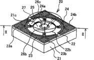
高亮度LED20包括:具有长方体并由具备高导热率的铜合金的金属芯材料制成的基座21,以及通过粘合剂22a固定到与散热面21a底面相对的基座顶面的布线盘22。布线盘是半固化片并具有绝缘性能。The
一对导电图形23和24通过铜箔形成在布线盘22上。导电图形23和24在各自转角处具有终端部分23a、23b、24a和24b作为连接面。与基座21的散热面21a相对安置终端部分23a、23b、24a和24b,并插入布线盘22和基座21。A pair of
具有圆形状的装配开口形成在布线盘22内以裸露基座21顶面的装配区21c。将作为发光芯片的LED元件25装配到装配区21c上并通过具备导热性的银膏25a将其固定到该区。由此,通过银膏25a将LED元件25热连接到基座21。A fitting opening having a circular shape is formed in the
通过四个引线26a、26b、26c和26d将一对正电极和一对负电极(未示出)电气连接到导电图形23、24。为了得到高亮度LED,较大的驱动电流是必要的。为此,最好通过两个导线分别将强电流施加到LED元件的正电极和负电极。用封装部件将LED元件25、导线26a-26b和部分布线盘22密封起来以保护这些部件。A pair of positive electrodes and a pair of negative electrodes (not shown) are electrically connected to the
当驱动电流被施加到导电图形23和24时,通过导线26a-26d将电压施加给LED元件25。从而驱动LED元件25消耗电能以产生能量。部分能量变成光线透过封装部件27放射出来,而大部分能量变成热量从LED元件放射而出。通过银膏25a将LED元件的热量传导到具备优良导热性的基座21。从而将热量有效地传送到的基座21。When a driving current is applied to the
如果将具备大热容的散热部件粘附到基座21底面的散热面21a,基座21的热量就被转移到散热部件,由此实现有效的散热。If a heat dissipation member having a large heat capacity is attached to the
在该实施例中,虽然提供了一个LED元件,但基座21被做成细长板,可以在基座上装配多个LED元件。并且,可以将多个布线盘22固定到基座21的顶面以便形成装配区21c。In this embodiment, although one LED element is provided, the
图3是依照本发明第二实施例的高亮度LED的立体图。FIG. 3 is a perspective view of a high brightness LED according to a second embodiment of the present invention.
用与图1和2中同样的标号表示与第一实施例相同的部分。The same parts as those of the first embodiment are denoted by the same reference numerals as in Figs. 1 and 2 .
高亮度LED30具有具备长方体并由具备高导热率的铜合金的金属芯材料制成的基座31。通过粘合剂将布线盘22固定到基座31的顶面。由于布线盘22、LED元件25和封装部件27与第一实施例的相同,以下省略其说明。The high-
在基座31的底面上形成多个平行散热片31a以增大散热面积。A plurality of
当驱动电流被施加到的LED元件25时,就驱动LED元件25消耗电能以产生能量。部分能量变成光线透过封装部件27放射而出,而大部分能量变成热量从LED元件放射而出。LED元件的热量被有效地传导到基座31。由于在基座31的底面上提供了多个散热片31a,热量被有效地散发以冷却LED元件25。如果提供一个冷却风扇来冷却LED元件25,就可以更有效地实现散热。可以在基座31的侧壁形成这些散热片。When a driving current is applied to the
图4是依照本发明第三实施例的高亮度LED的立体图。FIG. 4 is a perspective view of a high brightness LED according to a third embodiment of the present invention.
用与图1和2中同样的标号表示与第一实施例相同的部分,并省略其说明。The same parts as in the first embodiment are denoted by the same reference numerals as in Figs. 1 and 2, and descriptions thereof are omitted.
高亮度LED40具有具备长方体并由具备高导热率的铜合金的金属芯材料制成的基座41。The high-
在基座41的一个侧面形成了与基座底面平行的多个散热圆孔41a。孔41a最好是贯通的。如果将导热材料插入该孔,就可以提高散热效果。A plurality of heat dissipation circular holes 41 a parallel to the bottom surface of the base are formed on one side of the
图5是依照本发明第四实施例的高亮度LED的立体图,而图6是沿图5的VI-VI线的剖视图。FIG. 5 is a perspective view of a high brightness LED according to a fourth embodiment of the present invention, and FIG. 6 is a cross-sectional view along line VI-VI of FIG. 5 .
用与图1和2中同样的标号表示与第一实施例相同的部分,并省略其部分说明。The same parts as in the first embodiment are denoted by the same reference numerals as in Figs. 1 and 2, and part of their descriptions are omitted.
高亮度LED50具有具备长方体并由具备高导热率的铜合金的金属芯材料制成的基座51。The high-
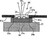
在基座51的转角处形成圆柱形突起物51a。在突起物上提供终末部51b作为端电极。布线盘22由于突起物51a而凹陷。终端部分51b的高度大于终端部分23a、23b的高度。
LED元件52具有在其顶面上的正电极52a和在底面上的负电极52b。正电极52a通过导线26a连接到终端部分23a而负电极52b通过基座51电气地连接到突起物51a的终端部分51b。The
当从终端部分23a和51b将驱动电流施加到LED元件52时,驱动LED元件52消耗电能以产生能量。部分能量变成光,而大部分能量变成热量从LED元件放射而出。将LED元件的热量有效地传导到基座51以冷却LED元件52。When a driving current is applied to the
依照第四实施例,将基座51用作引导部件。因此,可以使用在顶面和底面上具有电极的LED元件。According to the fourth embodiment, the
图7是依照本发明第五实施例的高亮度LED的立体图。FIG. 7 is a perspective view of a high brightness LED according to a fifth embodiment of the present invention.
用与图1和2中同样的标号表示与第一实施例相同的部分。The same parts as those of the first embodiment are denoted by the same reference numerals as in Figs. 1 and 2 .
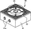
发光设备60包括:第四实施例的高亮度LED20,作为基底的印刷基底61,以及具备导热性的导热部件。The light-emitting
印刷基底61具有在其底面的铜箔导电图形和圆形通孔61b。封装部件27从孔61b伸出并将从LED元件25发射的光线作为放射光63而放射出。利用焊剂61c将导电图形61a电气和机械地连接到终端部分23a、23b、24a和24b。将散热部件62固定到基座21的以热连接到散热面21a。The printed
当通过导电图形61a将驱动电流施加给终端部分23a、23b、24a和24b以将驱动电流供给LED元件25时,驱动LED元件25发光。透过封装部件27将光线作为放射光63放射来。从LED元件散发的热量被传导到基座21和散热部件62。When a driving current is applied to the
依照第五实施例,通过基座21将从LED元件散发的热量有效地传导到散热部件62以将热量散发到空气。从而将LED元件中的热量增加控制在最小限度。因此,可以提供一种经受得起强电流驱动以发射高亮度光线的发光设备。此外,依靠散热效果,可以防止由高热引起的LED元件中接头的退化和由高热引起的封装部件27的变色而带来的亮度降低,由此得到具备高可靠性和长寿命的发光设备。According to the fifth embodiment, the heat dissipated from the LED element is efficiently conducted to the
远离基座21的散热面21a来安置连接到终端部分23a、23b、23c和23d的印刷基底61。因此,印刷基底61没有必要具有散热作用,由此,没有必要利用诸如金属芯的具备高导热率的昂贵材料来制作它。从而,可以自由选择诸如玻璃环氧树脂的便宜材料。The printed
为了增强散热部件62的散热效果,最好增大部件的面积或者在部件的表面形成多个突起物。虽然在第五实施例中使用了第一实施例的LED20,但是也可以使用任何另一个实施例的元件。在使用第二实施例的情况下,由于基座31具备较高的散热效果,就没有必要使用散热部件62。In order to enhance the heat dissipation effect of the
图8是显示本发明第六实施例的立体图。用同样的标号表示与图4显示的第三实施例相同的部分。发光设备70包括:第三实施例的高亮度LED40,一对作为热传导部件的热管71和由具备导热性材料制成的散热盘72。在热管71中,充满具有导热性的液体。Fig. 8 is a perspective view showing a sixth embodiment of the present invention. The same parts as those of the third embodiment shown in FIG. 4 are denoted by the same reference numerals. The light-emitting
各个热管71的末端插入到基座41的散热孔41a,热管71的另一端固定到散热盘72以便基座41热连接到散热盘72。An end of each
当驱动电压施加到LED元件25时,驱动LED元件25发射光线。光线被当作放射光放射而出。通过热管71将从LED元件放射出的热量有效地传导到基座41和散热盘72。When a driving voltage is applied to the
依照第六实施例,将LED元件25装配到具备导热性的基座41上以便热连接,基座41热连接到热管71,热管热连接到散热盘72。散热盘72有效地将传导的热量散发到空气中。从而,可以将LED元件中的热量升高控制在最小限度。因此,可以提供一种经受得强电流驱动以发射高亮度光线的发光设备。According to the sixth embodiment, the
由于可以用热管71彼此隔离热辐射元件40和散热盘72,可以提供在系统中容易组装的热辐射装置。Since the
按照第五实施例,印刷基底(未示出)没有必要具备散热作用,从而没有必要利用诸如金属芯的具备高导热率的昂贵材料来制造基底。According to the fifth embodiment, it is unnecessary for the printing substrate (not shown) to have a heat dissipation effect, so that it is not necessary to use an expensive material having a high thermal conductivity such as a metal core for the substrate.
为了增强散热盘72的散热效果,最好改变盘的形状,并可以增加热管71的数量。可以通过具备导热性的粘合剂来连接基座41和热管71。In order to enhance the heat dissipation effect of the
图9是显示本发明第七实施例的立体图。用同样的标号表示与第一实施例相同的部分。发光设备80包括:多个第一实施例的高亮度LED20,柔性印刷基底81和弓形散热部件82。Fig. 9 is a perspective view showing a seventh embodiment of the present invention. The same parts as those of the first embodiment are denoted by the same reference numerals. The
柔性印刷基底81具有插入LED20的封装部件27的三个通孔81a、81b和81c。通过焊剂83将印刷基底81的导电图形连接到LED20的终端部分。散热部件82具有三个凹座82a、82b和82c,LED20的基座21插入并固定到各个凹座内以使它们热连接。The flexible printed
当通过印刷基底81将驱动电流施加给高亮度LED20时,LED元件25就发射光线84a、84b和84c。通过基座21将从LED元件25排放的热量传导到散热部件82以便将热量散发。When a driving current is applied to the
根据本发明的第七实施例,将一些LED元件25装配到散热部件上以便于热连接。散热部件82有效地将传送的热量散发到空气。由此将LED元件中的热量升高控制在最小限度。因此,可以提供一种经受得强电流驱动以发射高亮度光线的发光设备。According to the seventh embodiment of the present invention, some
如第五实施例,印刷基底81没有必要具有散热作用,从而没有必要利用诸如金属芯的具备高导热率的昂贵材料来制造它。Like the fifth embodiment, it is not necessary for the
在发光设备80中,提供了多个高亮度LED20。因此,例如当安置了红色、黄色和绿色的高亮度LED时,就可以提供用于发射各种颜色光线的发光设备。In the
由于将高亮度LED20装配到可塑散热部件82上,可以通过将散热部件82弯曲成凸起形状从而聚集或散射所放射的光,如图9所示。Since the high-
以下,依照图10-15说明同时制造多个高度LED的方法。Hereinafter, a method for simultaneously manufacturing multiple height LEDs will be described with reference to FIGS. 10-15 .
图10是显示布线盘集合体90和基座集合体91的立体图。布线盘集合体90由一种绝缘材料制成并具有四个分区。在各个分区中,通过铜蚀刻(etchingof copper)形成导电图形90(91)a并形成了装配孔90b。基座集合体91由具备导热率的金属芯制成。FIG. 10 is a perspective view showing a
图11是显示布线盘集合体90和基座集合体91的组合步骤的立体图。通过粘合剂将布线集合体90固定到基座集合体91的表面以形成结合布线盘的基座集合体92。FIG. 11 is a perspective view showing a step of assembling the
图12是显示LED元件装配步骤的立体图。将LED元件93装配到结合布线盘的基座集合体92上的装配孔90b的裸露部分,并通过银膏将其固定。Fig. 12 is a perspective view showing an LED element assembly step. The
图13是显示导线焊接步骤的立体图。通过四个导线将LED元件93的电极连接到导电图形90a。Fig. 13 is a perspective view showing a wire bonding step. The electrodes of the
图14是显示封装步骤的立体图。通过透明树脂的封装部件95对各个分区中的LED元件93和导线94进行封装。由此,各个LED被固定在结合布线盘的基座集合体92上。Fig. 14 is a perspective view showing a packaging step. The
如图16所示,以分区之间的边界对结合布线盘的基座集合体92进行分割以便得到一个单体LED96。As shown in FIG. 16 , the wiring board-bonded
由此,根据本发明,可以以很低的成本同时制造大量LED。Thus, according to the invention, a large number of LEDs can be produced simultaneously at very low cost.
如果封装部件27中包含光散射剂(agent)、荧光物质或光束衰减剂,就可以提供一种在发射光的方向和波长方面不相同的各种高亮度LED和设备。If a light-scattering agent, a phosphor, or a beam attenuator is contained in the
依照本发明,将LED元件装配在具备高导热率的基座上。因此,可以有效地将LED中产生的热量传导给基座,以便可以提供具备优良散热效果的高亮度LED。According to the present invention, the LED element is mounted on a submount having high thermal conductivity. Therefore, heat generated in the LED can be efficiently conducted to the base, so that a high-brightness LED with an excellent heat dissipation effect can be provided.
虽然已经结合优选实施例描述了本发明,但应理解为,本说明书是描述本发明而并非限制由后附的权利要求书限定的本发明的范围。While the invention has been described in connection with preferred embodiments, it should be understood that this description describes the invention and does not limit the scope of the invention, which is defined by the appended claims.
Claims (13)
Applications Claiming Priority (2)
| Application Number | Priority Date | Filing Date | Title |
|---|---|---|---|
| JP2003052776AJP2004265986A (en) | 2003-02-28 | 2003-02-28 | High brightness light emitting element, light emitting device using the same, and method of manufacturing high brightness light emitting element |
| JP2003052776 | 2003-02-28 |
Publications (2)
| Publication Number | Publication Date |
|---|---|
| CN1617362A CN1617362A (en) | 2005-05-18 |
| CN100452448Ctrue CN100452448C (en) | 2009-01-14 |
Family
ID=32844547
Family Applications (1)
| Application Number | Title | Priority Date | Filing Date |
|---|---|---|---|
| CNB2004100078002AExpired - LifetimeCN100452448C (en) | 2003-02-28 | 2004-02-28 | Light emitting element and light emitting device with the light emitting element and method for manufacturing the light emitting element |
Country Status (4)
| Country | Link |
|---|---|
| US (3) | US7253447B2 (en) |
| JP (1) | JP2004265986A (en) |
| CN (1) | CN100452448C (en) |
| DE (1) | DE102004009998B4 (en) |
Families Citing this family (105)
| Publication number | Priority date | Publication date | Assignee | Title |
|---|---|---|---|---|
| JP2003309292A (en)* | 2002-04-15 | 2003-10-31 | Citizen Electronics Co Ltd | Metal core substrate for surface mounted light emitting diode and method of manufacturing the same |
| JP2004311791A (en)* | 2003-04-08 | 2004-11-04 | Sharp Corp | Lighting device, backlight device and display device |
| DE102004034166B4 (en) | 2003-07-17 | 2015-08-20 | Toyoda Gosei Co., Ltd. | Light-emitting device |
| JP2005236182A (en)* | 2004-02-23 | 2005-09-02 | Pentax Corp | Semiconductor light emitting device |
| JP2006086469A (en)* | 2004-09-17 | 2006-03-30 | Matsushita Electric Ind Co Ltd | Semiconductor light emitting device, illumination module, illumination device, and method for manufacturing semiconductor light emitting device |
| DE102004047324A1 (en)* | 2004-09-29 | 2006-04-13 | Osram Opto Semiconductors Gmbh | LED array |
| WO2006038778A1 (en)* | 2004-10-05 | 2006-04-13 | Samsung Electronics Co., Ltd. | Backlight unit |
| US7331691B2 (en)* | 2004-10-29 | 2008-02-19 | Goldeneye, Inc. | Light emitting diode light source with heat transfer means |
| US20100096993A1 (en)* | 2004-11-29 | 2010-04-22 | Ian Ashdown | Integrated Modular Lighting Unit |
| US20070273290A1 (en)* | 2004-11-29 | 2007-11-29 | Ian Ashdown | Integrated Modular Light Unit |
| KR100631903B1 (en)* | 2005-02-17 | 2006-10-11 | 삼성전기주식회사 | High power LED housing and its manufacturing method |
| JP2006245084A (en)* | 2005-03-01 | 2006-09-14 | Mitsubishi Electric Corp | Light emitting device |
| WO2006099741A1 (en)* | 2005-03-24 | 2006-09-28 | Tir Systems Ltd. | Solid-state lighting device package |
| WO2006105638A1 (en)* | 2005-04-05 | 2006-10-12 | Tir Systems Ltd. | Electronic device package with an integrated evaporator |
| US7633177B2 (en)* | 2005-04-14 | 2009-12-15 | Natural Forces, Llc | Reduced friction wind turbine apparatus and method |
| JP2006339224A (en)* | 2005-05-31 | 2006-12-14 | Tanazawa Hakkosha:Kk | LED substrate and LED package |
| WO2007013664A1 (en)* | 2005-07-27 | 2007-02-01 | Showa Denko K.K. | Light-emitting diode light source |
| JP2007036073A (en)* | 2005-07-29 | 2007-02-08 | Hitachi Displays Ltd | LIGHTING DEVICE AND DISPLAY DEVICE USING THE LIGHTING DEVICE |
| JP4759357B2 (en)* | 2005-09-28 | 2011-08-31 | 日立アプライアンス株式会社 | LED light source module |
| KR100767678B1 (en) | 2005-10-10 | 2007-10-17 | 엘지전자 주식회사 | LED cooling system |
| US8100567B2 (en)* | 2005-10-19 | 2012-01-24 | Rambus International Ltd. | Light-emitting devices and related systems |
| US20080099777A1 (en)* | 2005-10-19 | 2008-05-01 | Luminus Devices, Inc. | Light-emitting devices and related systems |
| US7771095B2 (en)* | 2005-10-26 | 2010-08-10 | Abl Ip Holding, Llc | Lamp thermal management system |
| US7488097B2 (en)* | 2006-02-21 | 2009-02-10 | Cml Innovative Technologies, Inc. | LED lamp module |
| US20070211183A1 (en)* | 2006-03-10 | 2007-09-13 | Luminus Devices, Inc. | LCD thermal management methods and systems |
| US7438440B2 (en)* | 2006-04-25 | 2008-10-21 | Abl Ip Holding Llc | Lamp thermal management system |
| US7906794B2 (en)* | 2006-07-05 | 2011-03-15 | Koninklijke Philips Electronics N.V. | Light emitting device package with frame and optically transmissive element |
| TWI363161B (en)* | 2006-07-26 | 2012-05-01 | Ind Tech Res Inst | Light emitting diode lighting module with improved heat dissipation structure |
| JP2008053660A (en)* | 2006-08-28 | 2008-03-06 | Matsushita Electric Works Ltd | Light emitting module |
| BRPI0718086A2 (en)* | 2006-10-31 | 2013-11-05 | Tir Technology Lp | LIGHTING DEVICE PACKAGING |
| TW200822384A (en)* | 2006-11-03 | 2008-05-16 | Coretronic Corp | LED package structure |
| WO2008060586A2 (en) | 2006-11-15 | 2008-05-22 | The Regents Of The University Of California | Textured phosphor conversion layer light emitting diode |
| WO2008060615A1 (en)* | 2006-11-15 | 2008-05-22 | The Regents Of The University Of California | Transparent mirrorless light emitting diode |
| US20080117597A1 (en)* | 2006-11-17 | 2008-05-22 | Foxconn Technology Co., Ltd. | Light emitting diode module having a thermal management element |
| DE102007056270B4 (en)* | 2006-11-24 | 2015-11-26 | Osram Gmbh | Lighting unit with an LED light source |
| JP4600455B2 (en)* | 2006-11-30 | 2010-12-15 | 東芝ライテック株式会社 | Lighting device |
| EP1928026A1 (en) | 2006-11-30 | 2008-06-04 | Toshiba Lighting & Technology Corporation | Illumination device with semiconductor light-emitting elements |
| EP2103191B1 (en)* | 2006-12-01 | 2016-04-27 | ABL IP Holding LLC | Systems and methods for thermal management of lamps and luminaires using led sources |
| JP2010512662A (en) | 2006-12-11 | 2010-04-22 | ザ リージェンツ オブ ザ ユニバーシティ オブ カリフォルニア | Transparent light emitting diode |
| DE102007017113A1 (en)* | 2007-01-31 | 2008-08-07 | Osram Opto Semiconductors Gmbh | Semiconductor device with an optically active layer, arrangement with a plurality of optically active layers and method for producing a semiconductor device |
| TW200847468A (en)* | 2007-05-23 | 2008-12-01 | Tysun Inc | Heat-dissipating substrates for light-emitting diodes |
| TW200847469A (en)* | 2007-05-23 | 2008-12-01 | Tysun Inc | Substrates of curved surface for light emitting diodes |
| US20090008662A1 (en)* | 2007-07-05 | 2009-01-08 | Ian Ashdown | Lighting device package |
| US7635205B2 (en)* | 2007-07-24 | 2009-12-22 | Fu Zhun Precision Industry (Shen Zhen) Co., Ltd. | LED lamp with heat dissipation device |
| DE102007046520A1 (en)* | 2007-09-28 | 2009-04-02 | Osram Opto Semiconductors Gmbh | Light-emitting surface element and method for producing a light-emitting surface element |
| DE102007057240A1 (en)* | 2007-11-28 | 2009-06-04 | Osram Opto Semiconductors Gmbh | Arrangement with a light-emitting module and a flexible conductor carrier |
| TWI488329B (en)* | 2008-05-15 | 2015-06-11 | Everlight Electronics Co Ltd | Circuit substrate and LED package |
| JP2009289543A (en)* | 2008-05-28 | 2009-12-10 | Rohm Co Ltd | Led lamp |
| TWM349665U (en)* | 2008-08-15 | 2009-01-21 | Enermax Technology Corp | Fan device with light emitting |
| TWD132818S1 (en)* | 2008-12-12 | 2010-01-01 | 億光電子工業股份有限公司 | Light-emitting diode device |
| TWM362513U (en)* | 2009-01-22 | 2009-08-01 | Yeh Chiang Technology Corp | Packaging structure for LED |
| JP2010272744A (en)* | 2009-05-22 | 2010-12-02 | Kyushu Institute Of Technology | LED module device and manufacturing method thereof |
| JP5499325B2 (en) | 2009-06-01 | 2014-05-21 | 東芝ライテック株式会社 | Light emitting module and lighting device |
| US8186852B2 (en)* | 2009-06-24 | 2012-05-29 | Elumigen Llc | Opto-thermal solution for multi-utility solid state lighting device using conic section geometries |
| JP2011159825A (en)* | 2010-02-01 | 2011-08-18 | Kyushu Institute Of Technology | Module device for led lighting, and method of manufacturing the same |
| US20110225818A1 (en)* | 2010-03-19 | 2011-09-22 | Shih-Bin Chiu | Method of manufacturing an led illuminator device |
| US8486761B2 (en)* | 2010-03-25 | 2013-07-16 | Koninklijke Philips Electronics N.V. | Hybrid combination of substrate and carrier mounted light emitting devices |
| US8319247B2 (en)* | 2010-03-25 | 2012-11-27 | Koninklijke Philips Electronics N.V. | Carrier for a light emitting device |
| CN102313157A (en)* | 2010-06-30 | 2012-01-11 | 可成科技股份有限公司 | Light-emitting diode lamp module with high heat dissipation efficiency and manufacturing method thereof |
| JP4910220B1 (en)* | 2010-10-19 | 2012-04-04 | 国立大学法人九州工業大学 | LED module device and manufacturing method thereof |
| TW201246618A (en)* | 2010-10-19 | 2012-11-16 | Kyushu Inst Technology | Led module device, method for manufacturing same, led package used for led module device, and method for manufacturing same |
| JP4914998B1 (en)* | 2010-11-17 | 2012-04-11 | 国立大学法人九州工業大学 | LED module device and manufacturing method thereof |
| USD712850S1 (en) | 2010-11-18 | 2014-09-09 | Cree, Inc. | Light emitter device |
| US8564000B2 (en) | 2010-11-22 | 2013-10-22 | Cree, Inc. | Light emitting devices for light emitting diodes (LEDs) |
| USD707192S1 (en) | 2010-11-18 | 2014-06-17 | Cree, Inc. | Light emitting device |
| US9000470B2 (en) | 2010-11-22 | 2015-04-07 | Cree, Inc. | Light emitter devices |
| US8624271B2 (en) | 2010-11-22 | 2014-01-07 | Cree, Inc. | Light emitting devices |
| USD706231S1 (en) | 2010-12-03 | 2014-06-03 | Cree, Inc. | Light emitting device |
| CN103415739B (en) | 2010-12-30 | 2015-03-04 | 伊路米根有限责任公司 | Light assembly having light sources and adjacent light tubes |
| CN102683507A (en)* | 2011-03-09 | 2012-09-19 | 神基科技股份有限公司 | Light source module structure and manufacturing method thereof |
| USD702653S1 (en) | 2011-10-26 | 2014-04-15 | Cree, Inc. | Light emitting device component |
| US8455908B2 (en) | 2011-02-16 | 2013-06-04 | Cree, Inc. | Light emitting devices |
| US8809880B2 (en)* | 2011-02-16 | 2014-08-19 | Cree, Inc. | Light emitting diode (LED) chips and devices for providing failure mitigation in LED arrays |
| JP4904604B1 (en)* | 2011-02-17 | 2012-03-28 | 国立大学法人九州工業大学 | LED module device and manufacturing method thereof |
| KR101881498B1 (en)* | 2011-02-22 | 2018-08-24 | 서울반도체 주식회사 | Light emitting diode package and method for manufacturing the same |
| JP4887529B1 (en)* | 2011-04-12 | 2012-02-29 | 国立大学法人九州工業大学 | LED package manufacturing method |
| KR20120128962A (en)* | 2011-05-18 | 2012-11-28 | 삼성전자주식회사 | Light emitting diode package and manufacturing method of the same |
| BR112013031560A2 (en) | 2011-06-09 | 2016-12-13 | Elumigen Llc | solid state lighting device using channels in a housing |
| USD705181S1 (en) | 2011-10-26 | 2014-05-20 | Cree, Inc. | Light emitting device component |
| KR20140097284A (en) | 2011-11-07 | 2014-08-06 | 크리,인코포레이티드 | High voltage array light emitting diode(led) devices, fixtures and methods |
| JP5942426B2 (en)* | 2011-12-28 | 2016-06-29 | 日亜化学工業株式会社 | Light source device |
| US10134961B2 (en) | 2012-03-30 | 2018-11-20 | Cree, Inc. | Submount based surface mount device (SMD) light emitter components and methods |
| US9735198B2 (en) | 2012-03-30 | 2017-08-15 | Cree, Inc. | Substrate based light emitter devices, components, and related methods |
| JP6019730B2 (en)* | 2012-05-14 | 2016-11-02 | オムロン株式会社 | Ultraviolet irradiation device and ultraviolet irradiation head |
| CN104112981A (en)* | 2013-04-18 | 2014-10-22 | 中国科学院物理研究所 | Cooling device for semiconductor laser device |
| JP6338136B2 (en)* | 2013-04-30 | 2018-06-06 | 東芝ライテック株式会社 | VEHICLE LIGHTING DEVICE AND VEHICLE LIGHT |
| USD739565S1 (en) | 2013-06-27 | 2015-09-22 | Cree, Inc. | Light emitter unit |
| USD740453S1 (en) | 2013-06-27 | 2015-10-06 | Cree, Inc. | Light emitter unit |
| JP6195760B2 (en)* | 2013-08-16 | 2017-09-13 | シチズン電子株式会社 | LED light emitting device |
| US9651219B2 (en) | 2014-08-20 | 2017-05-16 | Elumigen Llc | Light bulb assembly having internal redirection element for improved directional light distribution |
| JP6459880B2 (en)* | 2015-09-30 | 2019-01-30 | 日亜化学工業株式会社 | Light emitting device and manufacturing method thereof |
| EP3467887B1 (en)* | 2016-05-24 | 2022-01-26 | Citizen Electronics Co., Ltd. | Led lighting device and method for manufacturing led lighting device |
| JPWO2017209143A1 (en)* | 2016-05-31 | 2019-03-28 | シチズン電子株式会社 | Light emitting device and manufacturing method thereof |
| USD823492S1 (en) | 2016-10-04 | 2018-07-17 | Cree, Inc. | Light emitting device |
| USD831591S1 (en)* | 2017-01-20 | 2018-10-23 | Citizen Electronics Co., Ltd. | Light emitting diode |
| USD847769S1 (en)* | 2017-01-31 | 2019-05-07 | Citizen Electronics Co., Ltd. | Light emitting diode |
| JP6904720B2 (en)* | 2017-02-14 | 2021-07-21 | シチズン電子株式会社 | Luminous body |
| USD846510S1 (en)* | 2017-07-28 | 2019-04-23 | Lumens Co., Ltd. | Lens for LED package |
| USD840959S1 (en)* | 2017-07-28 | 2019-02-19 | Lumens Co., Ltd. | LED package |
| JP7064127B2 (en)* | 2017-09-29 | 2022-05-10 | 日亜化学工業株式会社 | Light emitting device and its manufacturing method |
| US11476399B2 (en) | 2017-11-29 | 2022-10-18 | Panasonic Intellectual Property Management Co., Ltd. | Jointing material, fabrication method for semiconductor device using the jointing material, and semiconductor device |
| US10810932B2 (en)* | 2018-10-02 | 2020-10-20 | Sct Ltd. | Molded LED display module and method of making thererof |
| US11592166B2 (en) | 2020-05-12 | 2023-02-28 | Feit Electric Company, Inc. | Light emitting device having improved illumination and manufacturing flexibility |
| US11876042B2 (en) | 2020-08-03 | 2024-01-16 | Feit Electric Company, Inc. | Omnidirectional flexible light emitting device |
| JP1695392S (en)* | 2020-12-02 | 2021-09-21 |
Citations (4)
| Publication number | Priority date | Publication date | Assignee | Title |
|---|---|---|---|---|
| JPH11298048A (en)* | 1998-04-15 | 1999-10-29 | Matsushita Electric Works Ltd | Led mounting board |
| CN2413390Y (en)* | 2000-02-24 | 2001-01-03 | 台湾光宝电子股份有限公司 | light emitting diode device |
| CN2508332Y (en)* | 2001-09-18 | 2002-08-28 | 林锡煌 | LED display |
| US6501103B1 (en)* | 2001-10-23 | 2002-12-31 | Lite-On Electronics, Inc. | Light emitting diode assembly with low thermal resistance |
Family Cites Families (21)
| Publication number | Priority date | Publication date | Assignee | Title |
|---|---|---|---|---|
| JPS62196878A (en) | 1986-02-25 | 1987-08-31 | Koito Mfg Co Ltd | Illumination system |
| JPH0383557U (en) | 1989-12-18 | 1991-08-26 | ||
| DE4005757A1 (en) | 1990-02-23 | 1991-08-29 | Bosch Gmbh Robert | Hand-tool machine with drill chuck - incorporates locking device preventing loosening of chuck jaws during operation |
| JPH0771131B2 (en) | 1990-09-27 | 1995-07-31 | 日本電気株式会社 | Internal failure monitoring device |
| JPH05218509A (en) | 1992-01-30 | 1993-08-27 | New Japan Radio Co Ltd | Optical semiconductor device |
| DE4336961C2 (en) | 1993-10-29 | 2000-07-06 | Kerafol Keramische Folien Gmbh | Flexible heat transfer device |
| JPH08129352A (en)* | 1994-10-31 | 1996-05-21 | Sukiru:Kk | Electric display sheet |
| US5857767A (en)* | 1996-09-23 | 1999-01-12 | Relume Corporation | Thermal management system for L.E.D. arrays |
| JP4135349B2 (en) | 1997-04-30 | 2008-08-20 | ソニー株式会社 | Agent display method, display device, agent parameter changing method and changing device |
| JPH11163412A (en) | 1997-11-25 | 1999-06-18 | Matsushita Electric Works Ltd | Led illuminator |
| JP4065051B2 (en)* | 1998-04-17 | 2008-03-19 | スタンレー電気株式会社 | Surface mount LED and manufacturing method thereof |
| JP3864263B2 (en) | 1999-08-24 | 2006-12-27 | ローム株式会社 | Light emitting semiconductor device |
| US6517218B2 (en) | 2000-03-31 | 2003-02-11 | Relume Corporation | LED integrated heat sink |
| JP3736366B2 (en)* | 2001-02-26 | 2006-01-18 | 日亜化学工業株式会社 | Surface mount type light emitting device and light emitting device using the same |
| JP3783572B2 (en) | 2001-03-05 | 2006-06-07 | 日亜化学工業株式会社 | Light emitting device |
| WO2002097884A1 (en) | 2001-05-26 | 2002-12-05 | Gelcore, Llc | High power led module for spot illumination |
| JP4045781B2 (en) | 2001-08-28 | 2008-02-13 | 松下電工株式会社 | Light emitting device |
| JPWO2003030274A1 (en)* | 2001-09-27 | 2005-01-20 | 日亜化学工業株式会社 | Light emitting device and manufacturing method thereof |
| US6498355B1 (en)* | 2001-10-09 | 2002-12-24 | Lumileds Lighting, U.S., Llc | High flux LED array |
| DE10260432A1 (en) | 2002-12-21 | 2004-07-08 | Ming, Fuh Lih, Tali | Rapid cooling LED for lighting has heat carried away via dielectric, substrate, leads and surface of gas-tight cover; substrate lamellas improve thermal exchange during generation of light energy |
| DE20219869U1 (en) | 2002-12-21 | 2003-05-15 | Ming, Fuh Lih, Tali, Taichung | Rapidly cooled light emitting diode has gas tight thermally conductive cover and cooling fins on the substrate |
- 2003
- 2003-02-28JPJP2003052776Apatent/JP2004265986A/enactivePending
- 2004
- 2004-02-24USUS10/784,242patent/US7253447B2/ennot_activeExpired - Fee Related
- 2004-02-28CNCNB2004100078002Apatent/CN100452448C/ennot_activeExpired - Lifetime
- 2004-03-01DEDE200410009998patent/DE102004009998B4/ennot_activeExpired - Fee Related
- 2007
- 2007-06-12USUS11/808,587patent/US7745835B2/ennot_activeExpired - Fee Related
- 2007-06-12USUS11/808,581patent/US7737462B2/ennot_activeExpired - Lifetime
Patent Citations (4)
| Publication number | Priority date | Publication date | Assignee | Title |
|---|---|---|---|---|
| JPH11298048A (en)* | 1998-04-15 | 1999-10-29 | Matsushita Electric Works Ltd | Led mounting board |
| CN2413390Y (en)* | 2000-02-24 | 2001-01-03 | 台湾光宝电子股份有限公司 | light emitting diode device |
| CN2508332Y (en)* | 2001-09-18 | 2002-08-28 | 林锡煌 | LED display |
| US6501103B1 (en)* | 2001-10-23 | 2002-12-31 | Lite-On Electronics, Inc. | Light emitting diode assembly with low thermal resistance |
Also Published As
| Publication number | Publication date |
|---|---|
| CN1617362A (en) | 2005-05-18 |
| US20070241361A1 (en) | 2007-10-18 |
| US20070246730A1 (en) | 2007-10-25 |
| US7253447B2 (en) | 2007-08-07 |
| DE102004009998B4 (en) | 2010-05-06 |
| DE102004009998A1 (en) | 2004-09-09 |
| US7737462B2 (en) | 2010-06-15 |
| US7745835B2 (en) | 2010-06-29 |
| JP2004265986A (en) | 2004-09-24 |
| US20040169451A1 (en) | 2004-09-02 |
Similar Documents
| Publication | Publication Date | Title |
|---|---|---|
| CN100452448C (en) | Light emitting element and light emitting device with the light emitting element and method for manufacturing the light emitting element | |
| CN100407453C (en) | Surface-mounted LED and light-emitting device using the same | |
| US7642704B2 (en) | Light-emitting diode with a base | |
| JP4123105B2 (en) | Light emitting device | |
| CN100514681C (en) | Light emitting device | |
| US7675086B2 (en) | LED assembly with high heat dissipating capability | |
| US8304279B2 (en) | Light emitting diode package having anodized insulation layer and fabrication method therefor | |
| TWI538255B (en) | Power surface mount light-emitting die package | |
| US20060091416A1 (en) | High power LED package with universal bonding pads and interconnect arrangement | |
| JP2005158957A (en) | Light emitting device | |
| KR20080030584A (en) | Semiconductor light emitting device package structure | |
| JP2004207367A (en) | Light emitting diode and light emitting diode arrangement plate | |
| JP4976982B2 (en) | LED unit | |
| JP4187239B2 (en) | High brightness light emitting device and manufacturing method thereof | |
| JP3938100B2 (en) | LED lamp and LED lighting fixture | |
| KR100764461B1 (en) | Semiconductor package with buffer layer | |
| JP2009021384A (en) | Electronic component and light emitting device | |
| KR20060009976A (en) | Heat sink integrated light emitting diode | |
| JP4655735B2 (en) | LED unit | |
| JP2017050342A (en) | Light emitting device | |
| JP2012119544A (en) | Led light emitting body | |
| KR100878398B1 (en) | High output LED package and manufacturing method | |
| KR100803161B1 (en) | LED package made of single crystal silicon and light emitting device using same | |
| TWI440207B (en) | The light emitting diode element is equipped with a light source | |
| KR20090113115A (en) | Leadframe with Effective Heat Dissipation Structure for High Power Light Source Lamp, Electronic Device and Manufacturing Method Thereof |
Legal Events
| Date | Code | Title | Description |
|---|---|---|---|
| C06 | Publication | ||
| PB01 | Publication | ||
| C10 | Entry into substantive examination | ||
| SE01 | Entry into force of request for substantive examination | ||
| C14 | Grant of patent or utility model | ||
| GR01 | Patent grant | ||
| CX01 | Expiry of patent term | Granted publication date:20090114 | |
| CX01 | Expiry of patent term |