CN100452424C - Optical device for LED-based light-bulb substitute - Google Patents
Optical device for LED-based light-bulb substituteDownload PDFInfo
- Publication number
- CN100452424C CN100452424CCNB2004800169230ACN200480016923ACN100452424CCN 100452424 CCN100452424 CCN 100452424CCN B2004800169230 ACNB2004800169230 ACN B2004800169230ACN 200480016923 ACN200480016923 ACN 200480016923ACN 100452424 CCN100452424 CCN 100452424C
- Authority
- CN
- China
- Prior art keywords
- region
- light
- emitter
- optical device
- led
- Prior art date
- Legal status (The legal status is an assumption and is not a legal conclusion. Google has not performed a legal analysis and makes no representation as to the accuracy of the status listed.)
- Expired - Lifetime
Links
- 230000003287optical effectEffects0.000titleclaimsabstractdescription51
- 238000012546transferMethods0.000claimsabstractdescription56
- 230000005855radiationEffects0.000claimsdescription17
- 230000003746surface roughnessEffects0.000claimsdescription7
- 239000012780transparent materialSubstances0.000claimsdescription7
- 239000007787solidSubstances0.000claimsdescription6
- 239000004606Fillers/ExtendersSubstances0.000claims2
- 239000003795chemical substances by applicationSubstances0.000claims1
- 238000007654immersionMethods0.000claims1
- 150000001875compoundsChemical class0.000abstract1
- 238000000034methodMethods0.000description16
- 238000009826distributionMethods0.000description15
- 238000010586diagramMethods0.000description11
- 230000000875corresponding effectEffects0.000description5
- 229910003460diamondInorganic materials0.000description5
- 239000010432diamondSubstances0.000description5
- 239000011521glassSubstances0.000description5
- 229920000515polycarbonatePolymers0.000description5
- 239000004417polycarbonateSubstances0.000description5
- 230000001902propagating effectEffects0.000description5
- 238000004364calculation methodMethods0.000description4
- 238000013461designMethods0.000description4
- 230000009467reductionEffects0.000description4
- NCGICGYLBXGBGN-UHFFFAOYSA-N3-morpholin-4-yl-1-oxa-3-azonia-2-azanidacyclopent-3-en-5-imine;hydrochlorideChemical compoundCl.[N-]1OC(=N)C=[N+]1N1CCOCC1NCGICGYLBXGBGN-UHFFFAOYSA-N0.000description3
- 229920000535Tan IIPolymers0.000description3
- 230000008901benefitEffects0.000description3
- 230000000694effectsEffects0.000description3
- 230000004907fluxEffects0.000description3
- 239000002184metalSubstances0.000description3
- 229910052751metalInorganic materials0.000description3
- 238000002156mixingMethods0.000description3
- 239000004033plasticSubstances0.000description3
- 229920003023plasticPolymers0.000description3
- 239000004593EpoxySubstances0.000description2
- NIXOWILDQLNWCW-UHFFFAOYSA-Nacrylic acid groupChemical groupC(C=C)(=O)ONIXOWILDQLNWCW-UHFFFAOYSA-N0.000description2
- 238000004458analytical methodMethods0.000description2
- 238000013459approachMethods0.000description2
- 230000008859changeEffects0.000description2
- 239000003086colorantSubstances0.000description2
- 238000009792diffusion processMethods0.000description2
- 238000002347injectionMethods0.000description2
- 239000007924injectionSubstances0.000description2
- 238000007689inspectionMethods0.000description2
- 238000004519manufacturing processMethods0.000description2
- 230000002829reductive effectEffects0.000description2
- 230000003362replicative effectEffects0.000description2
- 230000007704transitionEffects0.000description2
- 238000002834transmittanceMethods0.000description2
- RYGMFSIKBFXOCR-UHFFFAOYSA-NCopperChemical compound[Cu]RYGMFSIKBFXOCR-UHFFFAOYSA-N0.000description1
- 238000000342Monte Carlo simulationMethods0.000description1
- 239000004743PolypropyleneSubstances0.000description1
- 238000000149argon plasma sinteringMethods0.000description1
- 230000002238attenuated effectEffects0.000description1
- 230000002146bilateral effectEffects0.000description1
- 230000005540biological transmissionEffects0.000description1
- 230000001427coherent effectEffects0.000description1
- 239000000470constituentSubstances0.000description1
- 238000010276constructionMethods0.000description1
- 229910052802copperInorganic materials0.000description1
- 239000010949copperSubstances0.000description1
- 230000002596correlated effectEffects0.000description1
- 238000005314correlation functionMethods0.000description1
- 230000001186cumulative effectEffects0.000description1
- 238000005520cutting processMethods0.000description1
- 239000003989dielectric materialSubstances0.000description1
- 239000003822epoxy resinSubstances0.000description1
- 239000000835fiberSubstances0.000description1
- 238000010304firingMethods0.000description1
- 238000000227grindingMethods0.000description1
- 238000010438heat treatmentMethods0.000description1
- 238000003384imaging methodMethods0.000description1
- 230000003189isokinetic effectEffects0.000description1
- 230000000670limiting effectEffects0.000description1
- 238000004020luminiscence typeMethods0.000description1
- 238000003754machiningMethods0.000description1
- 238000000691measurement methodMethods0.000description1
- 230000007246mechanismEffects0.000description1
- 239000000203mixtureSubstances0.000description1
- 238000012986modificationMethods0.000description1
- 230000004048modificationEffects0.000description1
- 239000006060molten glassSubstances0.000description1
- 238000000465mouldingMethods0.000description1
- 230000036961partial effectEffects0.000description1
- 238000005192partitionMethods0.000description1
- 229920000647polyepoxidePolymers0.000description1
- 229920000379polypropylene carbonatePolymers0.000description1
- 230000000750progressive effectEffects0.000description1
- 230000001681protective effectEffects0.000description1
- 230000002441reversible effectEffects0.000description1
- 238000005070samplingMethods0.000description1
- 230000035945sensitivityEffects0.000description1
- 230000035939shockEffects0.000description1
Images


Classifications
- Y02B20/383—
Landscapes
- Non-Portable Lighting Devices Or Systems Thereof (AREA)
Abstract
Description
Translated fromChinese技术领域technical field
本发明涉及发光二极管(LED),尤其涉及用白光LED代替白炽灯泡和荧光灯泡的光学装置。This invention relates to light emitting diodes (LEDs), and more particularly to optical devices that replace incandescent and fluorescent bulbs with white LEDs.
背景技术Background technique
虽然花费昂贵,但是最新的白光LED仍可与输出小于100流明的传统白炽灯相比。在此低流明范围内,多数白炽应用是由电池供电的。期望有一种适于在例如烧坏的手电筒泡处直接安装的LED。Although expensive, the latest white LEDs are comparable to traditional incandescent lamps with an output of less than 100 lumens. In this low lumen range, most incandescent applications are battery powered. It would be desirable to have an LED suitable for direct mounting in, for example, the bulb of a burned out flashlight.
LED提供的发光效能超过在例如电池供电的手电筒中使用的传统白炽灯。此外,LED对冲击、振动和挤压应力的耐受度更高。虽然当前它们的生产成本要高于白炽灯,但是它们的使用寿命比白炽灯大大的延长。出于对效能的考虑,手电筒泡需要热中运行,所以它们在灯丝失效前通常仅可持续几个小时。而且LED的价格持续下降,而控制电子设备的LED也能够承受电池电压的变化。LEDs provide luminous efficacy that exceeds traditional incandescent lamps used, for example, in battery-operated flashlights. In addition, LEDs are more resistant to shock, vibration and crush stress. Although they are currently more expensive to produce than incandescent lamps, they have a much longer lifespan than incandescent lamps. For efficiency reasons, flashlight bulbs need to run hot, so they typically only last a few hours before the filament fails. And the price of LEDs continues to drop, and the LEDs that control the electronics are able to withstand changes in battery voltage.
虽然LED手电筒的确已经商业可用了,但是它们的光学器件必须要适应仅能发出半球形光的发光二极管的几何形状。传统的LED灯在电气上和光学上都不适于直接装入传统手电筒。LED灯电学上的不适合是因为它们是电流驱动设备,而电池是电压源。新电池电压上的典型变化就足以超出LED容许的工作电压范围。由此产生的电流是如此之高使得LED灯的管芯内部的欧姆热超过了热传导可移除的能力,从而引发温度上升的失控以致烧坏管芯。因此,LED灯必须配备电流控制设备。While LED flashlights are indeed commercially available, their optics must accommodate the geometry of light-emitting diodes, which only emit hemispherical light. Conventional LED lights are not electrically and optically suitable to fit directly into a conventional flashlight. LED lights are not suitable electrically because they are current driven devices and batteries are voltage sources. A typical change in the voltage of a new battery is enough to exceed the allowable operating voltage range of the LED. The resulting current is so high that the ohmic heat inside the die of the LED lamp exceeds the ability of heat conduction to remove, causing a runaway temperature rise that burns out the die. Therefore, LED lights must be equipped with current control equipment.
传统的LED灯在光学上不适于直接安装入手电筒的抛物面反射器。这是因为它们的子弹式的透镜结构形成的窄光束根本无法照到邻近典型的手电筒抛物面反射器。代替使用的是一种以位于发光管芯为中心的按半球形发光的无定向圆顶,提供了流传最广的市售可用朗伯模式光源,它对离开LED灯中心轴θ角所包围的光通量与sin2θ成正比。因为典型的抛物面手电筒反射器中θ值是从45°到135°,而由于LED灯的发光仅在θ=90°时就变为零,所以LED灯与半球模式不匹配。这导致了外部最亮而在内部到一半就完全暗下来的光束。更糟的是,即使是来自半球形LED的较差的内部光束模式也要求其保持在抛物面焦点处,也就是安装传统白炽灯泡灯座以上的几毫米处。Conventional LED lights are not optically suitable to fit directly into a flashlight's parabolic reflector. This is because their bullet-like lens construction creates a narrow beam that simply cannot reach the adjacent parabolic reflector of a typical flashlight. Instead, a hemispherical, non-directional dome centered on the light-emitting die provides the most widely available commercially available Lambertian mode light source, which has a wide range of angles from the central axis of the LED lamp surrounded by the angle θ. Luminous flux is proportional to sin2 θ. Because the θ value in a typical parabolic flashlight reflector is from 45° to 135°, and since the light emission of the LED light becomes zero only at θ = 90°, the LED light does not match the hemispherical pattern. This results in a beam that is brightest on the outside and completely dimmed halfway through the inside. To make matters worse, even the poor internal beam pattern from the hemispherical LED requires it to remain at the parabolic focus, a few millimeters above where a traditional incandescent bulb mounts.
另一种类型的电池供电灯用于圆柱形的荧光灯。虽然LED不能改善它们的发光效能,但是荧光灯是相对易碎的并且要求较高的电压。Another type of battery powered lamp is the cylindrical fluorescent lamp. While LEDs do not improve their luminous efficacy, fluorescent lamps are relatively fragile and require higher voltages.
因此本领域中就需要一种效率高、电压低并且光学上适用的LED灯,它通过直接将LED灯装入现有手电筒的抛物面反射器就可翻新现有的白炽灯泡手电筒。There is therefore a need in the art for a high efficiency, low voltage and optically acceptable LED lamp that can retrofit existing incandescent bulb flashlights by directly fitting the LED lamp into the existing flashlight's parabolic reflector.
发明内容Contents of the invention
本发明通过提供用基于LED灯泡的光学设备来代替白炽灯和荧光灯的较佳实施例,妥善地满足上述所有需要以及其他需要。The present invention satisfies all of the above needs, as well as others, by providing a preferred embodiment for replacing incandescent and fluorescent lamps with optical devices based on LED light bulbs.
在一个实施例中,本发明描述了用于分布光发射器的辐射发射的光学设备,所述光学设备包括下部传递区以及位于所述下部传递区之上的上部射出器区。所述下部传递区用于放置在光发射器上并且用于将辐射发射传递到所述上部射出器区。设计上部射出器区的形状使得向外的发射重新分布基本上呈立体角。In one embodiment, the present disclosure describes an optical device for distributing radiation emission from a light emitter, the optical device comprising a lower transfer region and an upper emitter region above the lower transfer region. The lower transfer region is for placement on a light emitter and for transferring radiation emissions to the upper emitter region. The shape of the upper injector region is designed such that the outward emission redistribution is substantially solid angle.
在另一个实施例中,本发明描述了用于分布光发射器的辐射发射的光学设备,所述光学设备包括由基本透明的材料所制成的多个离轴椭圆体。从每个椭圆体的焦点处起截去其顶部并且将其相互纵向耦合以提供内全反射通道。In another embodiment, the present invention describes an optical device for distributing radiation emission from a light emitter, the optical device comprising a plurality of off-axis ellipsoids made of a substantially transparent material. The top of each ellipsoid is truncated from its focal point and coupled longitudinally to each other to provide total internal reflection channels.
在另一个实施例中,本发明描述了用于分布光发射器的辐射发射的光学设备,所述光学设备具有扩展器区和圆柱形射出器区。所述扩展器区由基本透明的材料制成并且可用于接收所述辐射发射以及通过内全反射将所述辐射发射的角度范围缩小至光波导的角度范围。圆柱形射出器区耦合至扩展器区并且是由在所述圆柱形射出器区的表面上具有逐级子波长粗糙度的基本透明材料制成,同时用于接收并射出经角度窄化的辐射。In another embodiment, the present invention describes an optical device for distributing radiation emission from a light emitter, the optical device having an expander region and a cylindrical emitter region. The expander region is made of a substantially transparent material and is operable to receive the radiation emission and reduce the angular range of the radiation emission to that of the optical waveguide by total internal reflection. The cylindrical emitter region is coupled to the expander region and is made of a substantially transparent material having a progressive sub-wavelength roughness on the surface of the cylindrical emitter region while receiving and emitting angularly narrowed radiation .
通过参考随后的本发明的详细描述以及附图将可获得对本发明特性和优点的更好理解,所述附图阐明了其中利用本发明原理的说明性实施例。A better understanding of the nature and advantages of the invention will be obtained by reference to the ensuing detailed description of the invention together with the accompanying drawings which illustrate illustrative embodiments in which the principles of the invention are utilized.
附图说明Description of drawings
从随后连同附图一并示出的更具体描述中,本发明的上述和其他方面、特性和优点将更加显而易见,所述附图包括:The above and other aspects, features and advantages of the present invention will become more apparent from the more particular description which follows, taken in conjunction with the accompanying drawings, which include:
图1是根据本发明一个实施例的光学设备顶透视图;Figure 1 is a top perspective view of an optical device according to one embodiment of the present invention;
图2是根据本发明一个实施例并结合了图1中示出设备的光学设备顶透视分解图;Figure 2 is a top perspective exploded view of an optical device incorporating the device shown in Figure 1 according to one embodiment of the present invention;
图3是根据本发明一个实施例以剖面形式示出的并且结合了图2中示出设备的光学设备的顶透视分解图;3 is a top perspective exploded view of an optical device shown in cross-section and incorporating the device shown in FIG. 2 according to one embodiment of the present invention;
图4是根据本发明一个实施例并结合了图3中示出设备的光学设备的顶透视图;Figure 4 is a top perspective view of an optical device incorporating the device shown in Figure 3 according to one embodiment of the present invention;
图5是离轴内全反射的椭圆轮廓的图解,并示出了该椭圆的焦点性质;Figure 5 is an illustration of the profile of an ellipse for off-axis total internal reflection and shows the focal properties of the ellipse;
图6是根据本发明两个实施例类似于图1中光学设备的两个光学设备的透视图;其中较小的一个示出了由于降低了TIR条件使得轮廓缩小。Fig. 6 is a perspective view of two optical devices similar to the optical device of Fig. 1 according to two embodiments of the present invention; the smaller one showing reduced profile due to reduced TIR conditions.
图7a是根据本发明一个可选实施例的光学设备的顶透视图;Figure 7a is a top perspective view of an optical device according to an alternative embodiment of the present invention;
图7b是根据本发明一个实施例的图7a中示出的设备变体的侧视图;Figure 7b is a side view of a variant of the device shown in Figure 7a according to one embodiment of the invention;
图8a和图8b是根据本发明可选实施例的顶部为锥形的光学设备侧视图;8a and 8b are side views of an optical device with a tapered top according to an alternative embodiment of the present invention;
图9a到图9d是根据本发明可选实施例的其他光学设备的侧视图;Figures 9a to 9d are side views of other optical devices according to alternative embodiments of the present invention;
图9e是根据本发明另一个可选实施例的LED封装光学设备的侧截面图;Fig. 9e is a side sectional view of an LED packaged optical device according to another alternative embodiment of the present invention;
图10是具有多个传递区的光学设备的侧视图,并且描述了通过根据本发明一个实施例的用于代替管状荧光灯的设备的光传播;Figure 10 is a side view of an optical device having multiple transfer zones and depicts light propagation through the device for replacing tubular fluorescent lamps according to one embodiment of the present invention;
图11是描述了在图2中示出的传递区出口面14处光线密度的点图;Figure 11 is a point diagram depicting the light intensity at the
图12是根据本发明一个实施例两端各带一个LED并且作为荧光灯替代物的多区光学设备的侧视图;Figure 12 is a side view of a multi-zone optical device with LEDs at each end and as a fluorescent lamp replacement according to one embodiment of the present invention;
图13是图12的带有描绘来自一个光源的的图;Figure 13 is a diagram of Figure 12 with depictions from a light source;
图14是图12的带有描绘从在内部被全反射的一条光线散射出的光线的图;Figure 14 is a diagram of Figure 12 with a depiction of rays scattered from a ray that is internally totally reflected;
图15是根据本发明一个实施例两端各带一个LED的作为荧光灯替代物的光学设备的侧视图;Figure 15 is a side view of an optical device as a fluorescent lamp replacement with LEDs at each end according to one embodiment of the present invention;
图16是带有示出右向传播示范光线的图15中示出的光学设备的侧视图;Fig. 16 is a side view of the optical device shown in Fig. 15 with exemplary light rays propagating in the right direction;
图17是具有子波长表面粗糙度以及示出的通过该设备传播的示范光线的图15中示出的光学设备的侧视图;17 is a side view of the optical device shown in FIG. 15 with sub-wavelength surface roughness and exemplary light rays propagating through the device shown;
图18是描述了计算视角因数的球面投影方法的图17中示出的圆柱形射出器区的正截面图;FIG. 18 is an elevational cross-sectional view of the cylindrical injector region shown in FIG. 17 depicting a spherical projection method for calculating view factor;
图19是描述了光线的图17中示出的圆柱形射出器区的局部剖面透视图,所述光线对圆柱体内部表面法线以临界角发射并且以相同临界角与圆柱体相交;FIG. 19 is a partial cutaway perspective view of the cylindrical emitter region shown in FIG. 17 depicting light rays launching at a critical angle to the cylinder interior surface normal and intersecting the cylinder at the same critical angle;
图20a是示出了用于计算最佳粗糙度分布的坐标系统的图15中示出设备的侧透视图;Figure 20a is a side perspective view of the device shown in Figure 15 showing the coordinate system used to calculate the optimum roughness profile;
图20b是根据本发明一个实施例的扩展器区的顶透视近视图;Figure 20b is a top perspective close-up view of an expander region according to one embodiment of the invention;
图20c是示出了扩展器区边界光线的图20b中所示的扩展器区的侧视图;Figure 20c is a side view of the expander region shown in Figure 20b showing the expander region boundary rays;
图20d是示出了扩展器区输出的空间平均亮度的角度变化图;Figure 20d is a graph showing the angular variation of the spatially averaged luminance output by the expander region;
图20e是示出了带有正弦平方的图20d同一亮度相图示;Figure 20e is a diagram showing the same luminance phase of Figure 20d with sine squared;
图21a是描绘通过方向单位球面的方法计算辐射接收的方法的方向单位球面的图示;Figure 21a is a diagram of a directional unit sphere depicting a method of calculating radiation reception by the method of a directional unit sphere;
图21b是示出了与图21a所示同一单位球面的赤道平面图,带有圆柱体内部的局部表面法线为10°到90°的sinθ的圆;Figure 21b is a diagram showing the equatorial plane of the same unit sphere as shown in Figure 21a, with the local surface normal inside the cylinder being a circle of sin θ from 10° to 90°;
图22是示出了方向单位球面是怎样放置在所述圆柱形射出器内部的图20a中所示圆柱形射出器的局部侧面的透视剖面图;Figure 22 is a perspective cutaway view of part of the side of the cylindrical injector shown in Figure 20a showing how the directional unit sphere is placed inside the cylindrical injector;
图23a是示出了投射方向的赤道平面图,作为根据本发明一个实施例的圆柱形射出器的内部视图;Figure 23a is an equatorial plan view showing the direction of projection as an internal view of a cylindrical injector according to one embodiment of the present invention;
图23b是根据本发明的一个实施例所示出的由内全反射在圆柱形射出器内所捕获光线的角空间的等通量细分区图;Fig. 23b is a subdivision diagram of equal flux in the angular space of light captured in a cylindrical emitter by total internal reflection according to an embodiment of the present invention;
图23c是根据从0至500的反射号码标识的图23a左上部象限的近视图;Figure 23c is a close-up view of the upper left quadrant of Figure 23a identified according to reflection numbers from 0 to 500;
图24是根据本发明的一个实施例的对不同漫反射系数值的一盏灯镜面反射照度图;Fig. 24 is a graph of specular reflection illuminance of a lamp for different albedo values according to one embodiment of the present invention;
图25是根据本发明的一个实施例的具有来自两盏灯镜面反射照度对于不同漫反射系数值的亮度图;Figure 25 is a graph of luminance with specular illuminance from two lamps versus different albedo values in accordance with one embodiment of the present invention;
图26是根据本发明的一个实施例所示出的漫反射系数的线性分布图,该分布给出了如在此公开的视角因素方法所计算算出的均匀亮度。Figure 26 is a graph illustrating a linear distribution of albedo giving uniform brightness as calculated by the viewing angle factor method as disclosed herein, according to one embodiment of the present invention.
在各个视图中,相应的参考符号指代相应的组件。Corresponding reference characters indicate corresponding components throughout the several views.
具体实施方式Detailed ways
如下对认为是实践本发明现有最佳模式的描述不是出于限制性的意义,而仅仅是为了描述本发明的主要原理。本发明的范围应参考权利要求确定。The following description of what is believed to be the best mode available for practicing the invention is not intended to be limiting, but merely to illustrate the general principles of the invention. The scope of the invention should be determined with reference to the claims.
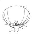
参见图1,示出了根据本发明一个实施例的光学设备的顶透视图。透镜10包括下部传递区11和上部射出器区12。Referring to Figure 1, a top perspective view of an optical device according to one embodiment of the present invention is shown. The
透镜10是形状大致为长椭球形的透明固体并且是诸如丙烯酸纤维或聚碳酸酯的单片透明材料。它具有长于其直径的旋转对称形状。上部的射出器区12是顶部具有圆锥形凹陷13的圆柱体。出口面14是传递区11和射出器区12间的边界。
下部传递区11使用内部反射向上重新安排LED的发射至抛物面的焦点。The
设计上部射出器区12的形状使得从其内部重新放射出上部射出器区的外表面的光张开的立体角基本上大于半球形,并且近似于手电筒白炽灯泡的光。射出器区放置高度必须与其代替的电灯泡发光灯丝相同。使用传递区光学地移动此发射点要比把LED本身放置在这一高度要容易,而将LED本身放置在这一高度会使得热转移变得困难,这也是本发明将有利地解决的问题之一。The shape of the
上部射出器区将传递光送出至抛物面反射器40(如下所述并在图4中示出),所述光对沿轴的侧及下方发射的角度可依据所述反射器达到至少135°或者更大一点。为了照亮反射器并形成强度足够的准直光束,应该有至少一半射出光角度大于45°。The upper emitter region sends the transmitted light out to a parabolic reflector 40 (described below and shown in FIG. 4 ), the angle of which the light is emitted to the side and down along the axis can be up to at least 135° or, depending on the reflector, bigger. In order to illuminate the reflector and form a collimated beam of sufficient intensity, at least half of the emitted light should have an angle greater than 45°.
为了避免传递区11的表面上有一外部反射层,传递区11的几何形状必须促进内全反射。这也是为什么具有更高折射率(1.5855)的聚碳酸酯要优于丙烯酸(1.492)的原因。其相应较小的临界角(θc=sin-1(1/n),39°103′对42°1′)使得传递区的高度从23.5 mm减至11.6 mm。In order to avoid an external reflective layer on the surface of the
接下来参见图2,根据本发明一个实施例并结合了图1中示出设备的光学设备顶透视分解图。示出的是圆对称透镜10以及三色LED 20。Referring next to FIG. 2 , a top perspective exploded view of an optical device incorporating the device shown in FIG. 1 , according to one embodiment of the present invention. Shown is a circularly
LED封装20包括填充有透明环氧树脂的白光散射反射杯21;发光二极管芯片22、23和24,将它们分别发出的红色、绿色、和蓝色光平衡混合成色温可选的白光色调。通过调节三个芯片22、23和24相对发光度实现所述色温的选择。透镜10的底部直径与反射杯21的顶部直径相匹配,而线25示出了透镜10和反射杯21的接合轨径。所有来自LED 20的光都被注入透镜10,并且在其内部发生的全反射穿过出口面14并进入射出器区12。LED封装20与透镜10的底部完全契合。在其他实施例中,这个光学填充可能不完全是为了透镜10能够与现有市售LED封装相结合。只要椭圆轮廓的焦点位于LED封装的发光周边上,透镜10就可截取来自LED封装所有的光。The
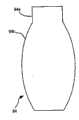
接下来参见图3,示出的是根据本发明一个实施例并结合了图2所示设备以剖面形式示出的光学设备顶透视图。图3示出了安装在灯泡替代物内的图2中示出的设备。示出的是透镜10、LED 20、桶形灯座30、位于带有电源耦合器32的板33上的LED控制电路、托盘34和透明玻璃泡35。Referring next to FIG. 3 , shown is a top perspective view of an optical device incorporating the device shown in FIG. 2 in cross-section, according to one embodiment of the present invention. Figure 3 shows the device shown in Figure 2 installed in a light bulb replacement. Shown are
以剖面形式示出安装在桶形灯座30上的透镜10和三色LED 20从而揭示内部的组件。这包括具有LED控制电路并带有连接至电绝缘底块31的电源耦合器32的板33,所述底块31通常是等效配置的白炽手电筒泡上的正极性点,而负极则连入其上安装有LED 20的托盘34。以剖面形式示出的保护性密封透镜10和LED 20的透明玻璃泡35。不像白炽灯泡。本实施例中的玻璃泡无需真空密封,因此就没必要评估在制作白炽灯泡时的泡形成时的温度以及用熔融玻璃液密封。泡35最好具有前透镜36,用于把来自透镜10的前向光线形成光束。The
泡35不仅在运作时保护透镜10与从三色LED 20的结合处被碰松以及防止工作时被弄脏,它还使得整个设备完全类似于要替代的白炽灯泡。但在此情况下,35内的玻璃不会变热。所以代替地,由托盘34为三色LED 20提供加热路径。The
泡35的另一个功能是颜色混合。在LED 20的发光操作期间,详细检查透镜体10将发现许多有色小闪光,这是三个有色芯片(即图2中的芯片22、23和24)之一上的微小光斑成的像。虽然这些闪光非常漂亮,但是如果期望抑制它们,那么随后可证明泡35表面的漫射体足以将这些闪光弥散以形成均匀的白光。可通过将(可被全息生成的)漫射体样式转移到模具金属上,由生产泡35的所述模具直接形成这些漫射体。所述全息漫射体使透射光发生衍射并具有较高的前向散射效率(即只有很少的光是向后散射的)。Another function of
桶形灯座30与白炽灯泡插口机械和电学可兼容,并且包括内置流控装置和诸如铜棒(板33上未示出)的散热装置以保护发光二极管芯片同时也能增加电流用来产生更高的管芯亮度。
接下来参见图4,示出的是根据本发明一个实施例并结合图3所示设备的光学设备的顶透视图。图4描绘了安装在抛物面反射器40内的图3所示设备,使得透镜10的上部位于抛物面反射器40的焦点上。桶形灯座30的形状以及电学配置都与其替代的白炽灯泡基本类似。Referring next to FIG. 4 , shown is a top perspective view of an optical device incorporating the device shown in FIG. 3 in accordance with one embodiment of the present invention. FIG. 4 depicts the device shown in FIG. 3 mounted within a
设备发出的至少一半光都直射入由抛物面反射器40填充的侧角,通常与抛物面反射器40的轴呈45°到135°的夹角。剩余的发光发射被前向送出而不返回管芯。桶形灯座30之上的泡35和透镜10与该设备替代的白炽灯泡的尺寸大体相同,而其主要的发射中心接近抛物面反射器40的焦点。在最低成本设计中,这通常接近白炽灯的顶部。At least half of the light emitted by the device is directed into the side angle filled by the
接下来参见图5,示出的是内全反射的离轴椭圆轮廓的图解,并示出了椭圆的焦点性质。Referring next to Fig. 5, shown is a diagram of an off-axis elliptical profile for total internal reflection, and illustrates the focal properties of the ellipse.
示出的是具有半长为a的长轴51和半长为b的短轴52的椭圆区段50。为了示出椭圆的全长,数学上将反射区段50继续延伸至上部短区段50μ和下部短区段50b。椭圆区段50绕中心轴53旋转生成用于图1所示传递区11的透镜形状。下部焦点54和上部焦点56与短轴52的距离都为c。下部焦点54辐射出光线扇形55等同于生成椭圆的弦方法。该光线扇形55由椭圆50反射至上部焦点56。最上角入射角57的值在所有组成光线扇形的光线中是最大的。如果入射角57(在下文中指定为θo)不小于临界角θc=sin-1(1/n),那么由椭圆区段50绕着轴53旋转形成的离轴椭圆表面将沿着其全长进行内全反射。Shown is an
将透镜的半径58指定为rw而将如图5中54s所示的光源半宽即半径59指定为rs。这些距离的和,即R=(rw+rs),以及边缘入射角θo确定椭圆50的形状和大小。两焦点间的距离为2c,并且R是由作为边界光线的光线55的第一或最后光线形成的三角形的底边。从所示三角形中可见Designate the
2c=R tan 2θo2c=R tan 2θo
椭圆50的边缘斜率是tan θo,对所述椭圆等式求微分得The edge slope of
b2=tan θo Ra2/cb2 =tan θo Ra2 /c
使用标准恒等式a2=b2+c2,可得:Using the standard identity a2 =b2 +c2 , we get:
聚碳酸酯 或者
接下来参见图6,示出的是根据本发明的两个实施例类似于图1所示设备的两个光学设备的顶部透视图,其中较小的一个示出了由降低对TIR条件的要求所达到的轮廓缩小。Referring next to FIG. 6, shown is a top perspective view of two optical devices similar to the device shown in FIG. The achieved contour shrinks.
在三色LED 20上的透镜10为在先前的图1到图4中示出,而完全TIR型式10a连同三色LED 20a一并示出。此外,这些泄漏也是有效地向前。θo值的减小能减小透镜10的高度,但是会有边界光线漏出。内全反射条件不强加在传递区11的整个表面,就导致为光线追踪所确定那样设备高度上的主要缩减可以在少于10%的适度泄漏的代价下发生。如果三色LED 20是朗伯型的,那么射到所述椭圆50近底部离法线夹角较大的地方就没什么能量。对比于图6所示的2∶1更大的高度降低,对填充所述透镜底部(rw=rs)朗伯型发射器作的蒙特卡洛模拟指出令人吃惊地仅有7%的损耗。The
接下来参见图7a,示出的是根据本发明可选实施例的光学设备的顶透视图。示出的是由离轴椭圆形传递区71和球形漫射射出器区72组成的透镜70。Referring next to Figure 7a, shown is a top perspective view of an optical device according to an alternative embodiment of the present invention. Shown is a
射出器区72的表面具有漫反射特性,使得射出器区72上每个点的亮度都与接收自传递区71的光成正比。此种射出器区的优点在于三色LED发出的不同波长在离开射出器区72之前就被混合。在上述无漫反射的射出器区12中,所述颜色混合可能不完全,这就导致诸如图4中所示的抛物面反射器输出光束的带色。射出器区72比传递区71要大(即其直径要大于传递区的中间直径),因而它具有面向下的区表面用来发送朝向抛物面反射器底部的光。该漫射体也如上述对图3的描述,混合在LED光源内部红、绿、蓝光源芯片的颜色光。也可使用产生不同输出模式的其他射出器区。The surface of the
接下来参见图7b,示出的是根据本发明一个实施例的图7a中所示设备变体的的侧视图。Referring next to Figure 7b, shown is a side view of a variation of the apparatus shown in Figure 7a, according to one embodiment of the present invention.
图7b示出了前述球形设计的变体。透镜75包括下部的离轴椭圆形传递区76和上部的球形射出器区77。因为射出器的尺寸较小,所以该变体比图7a中前一球形设计在90°以下的角度内辐射的较少。Figure 7b shows a variation of the aforementioned spherical design.
接下来参见图8a和图8b,示出的是根据本发明可选实施例的顶部为锥形的光学设备侧视图。Referring next to Fig. 8a and Fig. 8b, it shows a side view of an optical device with a tapered top according to an alternative embodiment of the present invention.
示出的是两个带有二次曲面射出器的透镜80和85的实施例。二次曲面包括由曲线以及直线形成的锥形物。图8a示出了由下部传递区81和沿着传递区81顶部的点起始的二次曲面射出器82组成的透镜80,其中二次曲面射出器82的底面直径小于传递区81的直径,从而产生由传递区81到射出器82的突变转变。图8b示出了由下部的传递区86和大于图8A所示锥形物的圆锥形射出器87组成的透镜85。此处的射出器87沿着传递区86顶部的点起始,其中二次曲面射出器82的底面直径等于传递区81的直径,从而产生由传递区81到射出器82的平滑过渡。诸如可为了图4所示的抛物面反射器,使用这些二次曲面射出器发送更少的前向光和更多的侧向光。Shown are two embodiments of
接下来参见图9a至图9d,示出的是根据本发明可选实施例的其他光学设备的侧视图。Referring next to Figures 9a to 9d, side views of other optical devices according to alternative embodiments of the present invention are shown.
图9a示出了由下部的传递区90t和椭圆射出器90e组成的透镜90,趋于产生相对较窄的向前光束,这样就无需抛物线镜面。图9b示出了由下部的传递区92t和在其顶部带有球形凹的窝眼式射出器92e组成的透镜92。图9c示出了由传递区94t和圆柱形射出器94e组成的透镜94。图9d描绘了由传递区96t和内部漫射圆柱形射出器96e组成的透镜96。Figure 9a shows a
接下来参见图9e,示出的是根据本发明可选实施例的LED封装光学设备的侧截面图。Referring next to Fig. 9e, there is shown a side cross-sectional view of an LED packaged optical device according to an alternative embodiment of the present invention.
关于带有LED的本发明的使用,在图9e中示出了一个可选的实施例。示出的是具有源芯片191、透明电介质192、引线框193、射出器区194、圆锥形凹195、上部传递区196、光学不活动灯座197、反射杯198和引线199的LED封装190。Regarding the use of the invention with LEDs, an alternative embodiment is shown in Figure 9e. Shown is an
为了便于集成生产,此较佳实施例作为包含有图3所示设备10的单片LED封装被集成地生产出来。LED封装190具有浸入透明电介质192并安放在引脚框193上的源芯片191。来自源芯片191的引线199可操作地连接至引线框193。射出器194具有圆锥形凹195并且在上部传递区196的顶上。类似于图9e中所有其他接近垂直的表面,光学不活动灯座197具有正向脱模。反射杯198起到下部传递区的作用。上部转移196经由内全反射进行工作。上部196和下部198两个传递区都在芯片191上和射出器区194的外部边缘上具有公共的焦点。To facilitate integrated production, the preferred embodiment is integrally produced as a monolithic LED package containing the
转到代替管状荧光灯的实施例,有两个定义新产品。第一个是带有插入射出器区的多个连续传递区的串型连接物。第二个是使得这些区的表面自身发生漫射发射的射出器区的代替物。Turning to the example of replacing tubular fluorescent lamps, there are two new products that define. The first is a tandem connection with multiple successive transfer zones inserted into the injector zone. The second is the replacement of the emitter regions with diffuse emission from the surfaces of these regions themselves.
当多个传递区连接成单个透镜体时,在一端注入的光将完全传递到另一端。When multiple transfer areas are connected into a single lens body, light injected at one end will be completely transferred to the other end.
接下来参见图10,示出的是具有多个传递区的光学设备的侧视图,并且描述了通过根据本发明一个实施例来代替管状荧光灯的设备的光传播。Referring next to FIG. 10, shown is a side view of an optical device having multiple transfer zones and depicts light propagation through the device replacing a tubular fluorescent lamp in accordance with one embodiment of the present invention.
示出的是由三个同样的离轴椭球体810、820和830组成的电介质体800的截面图。光源805发出的光线850向右进至端平面801。上述提及的TIR条件由这些离轴椭圆轮廓满足,使得它们具有如图6中更高区10a的比例。这样,所有的光学850经由多次内部发射到达端面801。具有多个这样的区的唯一原因是对于总体直径802的限制。例如通过小比例的重复,电池供电的荧光灯可以包括多于三个这样的椭球体。最好是在这一透镜的两端都具有LED。A cross-sectional view of a
这里提供了复制荧光灯发射的两个实施例。第一个是用插入射出器区来延续传递区。这些射出器的功能与先前讨论的手电筒泡的代用品能不同的原因有二。首先,光将从两个方向进入射出器区,是因为两端上都有LED。其次,角度输出范围仅是侧向的,没有如前讨论手电筒泡代替物的射出器区所要求的向前发射。Two examples of replicating the emission of fluorescent lamps are presented here. The first is to extend the transfer zone with an insert injector zone. These injectors function differently than the previously discussed flashlight bulb substitutes for two reasons. First, light will enter the emitter area from two directions because there are LEDs on both ends. Second, the angular output range is only lateral, without the forward firing required for the ejector region of the previously discussed flashlight bulb replacement.
传递区的出口面本身可看做一个具有特定外向光空间角度分布的源。来自于所述源的三种色光有各自的分布,这些光既有最初从图2所示的LED芯片22、23或24中的一个发射出来的,也有从圆锥形侧壁21漫反射的。传递区的离轴椭球体形状起到非成像光学设备的作用,其中入口处的原始空间角度分布在其出口处被强烈扰乱了。The exit face of the transfer zone can itself be considered as a source with a specific spatial angular distribution of outgoing light. There are respective distributions of the three colors of light from said sources, either initially emitted from one of the LED chips 22, 23 or 24 shown in FIG. The off-axis ellipsoidal shape of the transfer region acts as a non-imaging optical device in which the original spatial angular distribution at the entrance is strongly perturbed at its exit.
接下来参考图11,示出了在图2中传递区的出口面上描述光线密度的点图。在由一个颜色芯片发出并在其中内全反射之后的这些光线将离开传递区11。示出的是可追迹至一个芯片的20000条光线的分布900,具有其模糊图像的簇910以及对应于侧壁21的环形920,但是因为多次内部反射,所以大区的点还是随机分布的。这些更随机的多次反射光线具有朗伯型的角分布。这种光的空间角度分布对于射出器设计来说是很重要的,因为它决定光是怎样与射出器相交的。Referring next to FIG. 11 , there is shown a spot diagram depicting light intensity at the exit face of the transfer zone in FIG. 2 . These rays will leave the
接下来参考图12,示出的是根据本发明一个实施例作为荧光灯替代物并在其两端各具有一个LED的多区光学设备的侧视图。Referring next to FIG. 12 , shown is a side view of a multi-zone optical device as a fluorescent lamp replacement and having an LED at each end, according to one embodiment of the present invention.
图12示出了一个以发光设备100作为例证的较佳实施例,所述发光设备100带有光学连接到其塑料主体两端的LED封装101和102,其塑料主体包括离轴椭圆传递区111至116以及插入的漫射射出器区121至125。它们的相对长度确定它们截取多少光。它们的漫射透射比是由波长比例的粗糙度产生,其振幅确定有多少光被散射。Figure 12 shows a preferred embodiment exemplified by a
接下来参考图13,示出的是带有来自一光源的光线描述的图12所示设备。Referring next to FIG. 13, there is shown the apparatus of FIG. 12 with a depiction of light from a light source.
示出的是带有有源光源101由光线130表示的单片发射的发光设备100,可见所述光线经由内全反射向右传播。一系列的圆柱形射出器区121至125中的每一个都可截取进入光的三分之一,使得小量剩余光131仅代表了由有源光源101发出的光的很小一部分。这里没有示出射出器区是如何截取光的。Shown is a monolithically emitting
接下来参考图14,示出的是带有由被内全反射的一条光线散射出的光线的描述的图12中示出的设备。Referring next to FIG. 14 , shown is the device shown in FIG. 12 with a depiction of rays scattered by a ray that is totally internally reflected.
示出的是带有端光源101以及从中发射的光线130的发光设备100。光线132折射进入外部空气133。示出光线134由射出器区124进行内部反射,使得在到达与发光设备100的光源101相对端时还剩余更多的光线13 1。射出器区121、122、123、124和125的粗糙表面可使得射出器区成为有光线入射其上的漫反射散射器。粗糙度的恰当分布(如下文描述所确定)会使得仅剩余小量的图14中示出的光线131。Shown is a
精确复制荧光灯的发光表面发射首先要求在设备的全部表面一致发辉光,即它的全部都是射出器。其次另一可选的是图13和图14的多椭圆方法,即荧光灯本身的圆柱形。Accurately replicating the glowing surface emission of fluorescent lamps first requires uniform glowing across all surfaces of the device, ie all of it being the emitter. Next, another option is the multi-ellipse method shown in Fig. 13 and Fig. 14, that is, the cylindrical shape of the fluorescent lamp itself.
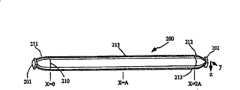
接下来参考图15,示出的是根据本发明一个实施例作为荧光灯替代物并在其两端各具有一个LED的光学设备的侧视图。Referring next to FIG. 15, shown is a side view of an optical device as a replacement for a fluorescent lamp and having an LED at each end in accordance with one embodiment of the present invention.
示出的是两端分别具有LED封装201和202的发光设备200。扩展器区211和212将来自源201和202的光引入圆柱体区213,该区通过在利用内全反射的设备中作为光学损耗源的现象(即由子波长粗糙度度所造成的散射)起到射出器区的作用。由于这种散射塑料光纤光学设备的长度受到限制,使之应用比玻璃少的多。图15中描述的实施例以仔细校准的方式结合了该现象从而产生了期望的表面发射。尽管如此,这种发射是由表面区213朝内的,而不像荧光灯那样是朝外的。Shown is a light emitting
接下来参考图16,示出的是具有示范性的右向传播光线的图15中光学设备的侧视图。Referring next to FIG. 16 , shown is a side view of the optical device of FIG. 15 with exemplary right-propagating rays.
示出了与图15中相同的透镜形状作为带有LED封装201和管状射出器区213的发光设备200。示出的典型光线220向右传播,并在点130处生内全反射。The same lens shape as in FIG. 15 is shown as a
在此对由Remillard,Everson和Weber发表在Applied Optics Vol.31,#34,pp7232-7241,December 1992的“Loss mechanisms in optical light pipes”作出其全文合并在此的参考。在其中明确的是,当所述粗糙度由高斯统计描述时,根据rms表面粗糙度σ方程式(8)示出了内部反射系数R0(TIR意味着R0=1)是如何约化为反射系数R,其中方程式为:Reference is hereby made to "Loss mechanisms in optical light pipes" by Remillard, Everson and Weber, Applied Optics Vol. 31, #34, pp7232-7241, December 1992, which is incorporated herein in its entirety. In it it is clear that when said roughness is described by Gaussian statistics, equation (8) shows how the internal reflection coefficient R0 (TIR means R0 =1) reduces to reflectance in terms of rms surface roughness σ Coefficient R, where the equation is:
Rspec=R0 exp[-(2KLσ)2]Rspec =R0 exp[-(2KL σ)2 ]
其中KL=2πcosθ/波长是与表面垂直的波数,对于入射角θ>θc,在折射率为n的介质内。对于波长为0.5微米(500 nm)并且n=1.58(θc=sin-1(1/n)=39.3°),所以cosθ<0.77并且KL=15,288/mm=15.3/μm。whereKL = 2πcos θ/wavelength is the wavenumber perpendicular to the surface, in a medium of refractive index n for angles of incidence θ > θc . For a wavelength of 0.5 microns (500 nm) and n=1.58 (θc =sin−1 (1/n)=39.3°), so cos θ<0.77 and KL =15,288/mm=15.3/μm.
表1Table 1
散射辐射的亮度B(x)是漫反射系数Rdiff(x)=1-Rspec(x)和入射光的照度I(x)的乘积,因此它随着粗糙度σ快速增。通过在沿着射出器区的不同距离x处变化粗糙度就能产生分级的散射量,以获得近似相同的亮度B(x)。应注意到散射水平越高就对波长越敏感,因而越不适用于需要颜色混合的场合的应用。The brightness B(x) of diffuse radiation is the product of the reflectance Rdiff (x) = 1 - Rspec (x) and the illuminance I(x) of the incident light, so it increases rapidly with the roughness σ. A graded amount of scattering can be produced by varying the roughness at different distances x along the emitter region to obtain approximately the same brightness B(x). It should be noted that higher levels of scattering are more sensitive to wavelength and thus less suitable for applications where color mixing is required.
由此受控子波长粗糙度形成的发射角度模式取决于其子波长空间相关函数C(x,Δx)的结构,它测量x处特定的随机粗糙轮廓与离开它一个微小距离Δx处内其他轮廓的相似程度。完全不相关的粗糙度将导致均匀的朗伯发光,而相同程度的粗糙空间相关性将导致亮度上角度上的方向变化,这会成为可见的非期望的亮度不均匀。The emission angle pattern formed by this controlled sub-wavelength roughness depends on the structure of its sub-wavelength spatial correlation function C(x, Δx), which measures a specific random rough profile at x and other profiles at a small distance Δx away from it degree of similarity. A completely uncorrelated roughness will result in a uniform Lambertian luminescence, while the same degree of spatial correlation of roughness will result in an angularly directional variation in brightness, which becomes visible as an undesired brightness non-uniformity.
无论如何,以上列出粗糙度的最低量(1-5nm),是由最佳金刚石削得到的更典型的剩余粗糙度。虽然在接近发射管长度的正中心处可能需要完全散射(Rdiff-1),但是0.8>Rdiff>0.2范围的中等水平更适合本发明。However, the lowest amount of roughness listed above (1-5nm) is the more typical residual roughness obtained by optimal diamond grinding. Moderate levels in the range of 0.8 > Rdiff > 0.2 are more suitable for the invention, although complete scattering (Rdiff-1 ) may be desired near the very center of the tube length.
用于全内反射的子波长粗糙度的重要性在于此粗糙度范围下所有的光都是相干的并受到衍射,而衍射又依次通过反射光的相位扰动产生非镜面反射。非镜面反射是散射的另一种叫法,但要注意到这种散射都不在电介质体外部,所以散射光都不会穿过所述表面进入周围的空气。只有在粗糙度接近波长尺度时,也就是上述全息漫射的情况下才能达到所述效果。当粗糙度为波长的1%时,即在此较佳实施例的情况下,所有的散射都是反射性的。此外,该散射只作用于圆柱体内引导的全内反射光。因此它并不类似于作用在透射光的全息漫射。而是子波长粗糙度散射反射光的一部分,无论它是在折射界面上的菲涅尔反射还是内全反射。The importance of sub-wavelength roughness for total internal reflection is that all light in this roughness range is coherent and subject to diffraction, which in turn produces non-specular reflection through phase perturbation of the reflected light. Non-specular reflection is another name for scattering, but note that none of this scattering is outside the dielectric body, so none of the scattered light passes through the surface into the surrounding air. Said effect is only achieved when the roughness is close to the wavelength scale, ie in the case of holographic diffusion as described above. When the roughness is 1% of the wavelength, which is the case in the preferred embodiment, all scattering is reflective. Furthermore, this scattering only acts on TIR light guided inside the cylinder. Therefore it is not similar to holographic diffusion acting on transmitted light. Rather, sub-wavelength roughness scatters a portion of the reflected light, whether it is Fresnel reflection or total internal reflection at a refractive interface.
粗糙度反射光从透镜10的表面被反射回射出器区213,但并不只沿着镜面反射的方向,而是沿着所有的方向。该散射光的一部分随后将对局部曲面法线有比临界角度小的入射角度,并在下一次遇到与其散射点相对的侧面时离开所述设备。当检查揭示了光是来自内部时,仔细观察所述透镜就可看到该散射光的内部原始光。子波长粗糙度不影响光的镜透射比,所以与先前讨论的单独给予折射光额外偏移的全息散射体不同,从透镜离开的光只服从斯涅尔定律。与全息散射体的波长尺度的粗糙度不同,本发明所利用的子波长粗糙度对于通过它的折射光无影响——只有其菲涅尔反射光被散射。The roughness reflected light is reflected from the surface of the
接下来参考图17,示出的是带有子波长表面粗糙度以及示出通过该设备传播的示范光线的图15中光学设备的侧视图。Referring next to FIG. 17, shown is a side view of the optical device of FIG. 15 with sub-wavelength surface roughness and illustrating exemplary light rays propagating through the device.
示出的是同样具有管状喷射区213的光源200,并且其现在具有子波长表面粗糙度。因此从图16中的LED 201封装发射的光线220将导致从TIR点发出的半球状光线扇形240。光线241从表面213射向空气中。由于全内反射俘获了光线242,故其留在透镜213内部。每次这一光线被内反射,它的部分通量都依次被散射。Shown is a
射出器213的圆柱形作为透镜放大观察者面对的内表面。其对这种聚丙烯或聚碳酸酯的塑料大约有4倍的放大倍数,这种放大倍数在划痕处和其他的表面裂隙处尤为突出,其中包括子波长粗糙度的任何不一致。这种表面粗糙度的不一致通过其引起的亮度的不一致体现。这种圆柱形放大意味着实际上只有很小一部分,1/4π=8%的发光周长可以从任意特定的有利点观察到。The cylindrical shape of the
接下来参考图18,所示的是计算视角因数的球体发射方法的图17圆柱形射出器区的正截面图。Referring next to FIG. 18, shown is a front cross-sectional view of the cylindrical injector region of FIG. 17 for the spherical launch method of calculating view factor.
子午光线扇形180代表了最初从射出器213内表面散射出来的光线。它在射出器213的另一面被折射出去并传播到左侧的观察点(未示出)相遇。从那个观察点,区域182看上去是被放大并充满射出器区213的整个图像。边缘光线181看来像是最初从射出器区213的边缘部分发出的,但实际上是来自区域182的中心。该边缘光线较大的入射角减小了它的透射系数,在射出器区213的发光面产生微弱的边缘暗带。对于沿管内的坐标x,适当的粗糙度σ(x)分布可为射出器区提供相当均匀的亮度。The
计算适当的粗糙度分布σ(x)则进入了相反问题的范畴。所述射出器区213的圆柱几何形状有助于其基于所述管的内表面细薄环域的数学分析。在图15中等于13∶1的管长与直径的纵横比也将起作用。来自扩展器部分的导行光线向下传播到所述管并且在每个长度坐标x上,它的一部分被由粗糙度σ(x)散射,而剩余光则发生镜面反射,其中反射率R由上表给出。该粗糙度散射的光只有40%从管的另一端折射出去,而剩余光将添加到导行光线帮助亮度更加均匀。Computing the appropriate roughness distribution σ(x) enters the realm of the reverse problem. The cylindrical geometry of the
一旦射入射出器区体,那么粗糙度散射光就受到内全反射的附加影响。Once entering the emitter region, the roughness scattered light is additionally affected by total internal reflection.
接下来参考图19,示出的是描述了光线的图17中示出的圆柱形射出器区的部分剖面透视图,所述光线与圆柱体内表面的法线成临界角发射并且以同一临界角与圆柱体相交。Referring next to FIG. 19, shown is a partially cutaway perspective view of the cylindrical emitter region shown in FIG. Intersect the cylinder.
图19示出了在圆柱191内表面的散射点190(简明起见只示出了圆柱体的一半)。作为光线锥体192的源的点190以与局部曲面法线呈θc角发射,其中示出了三个象限,并且一个象限将被折射入外部空气。示范光线193如图所示以将近90度的入射角折射进入外部空气。非相关的表面粗糙度将导致朗伯型的散射光,因此少部分的射出光将会是那些与法线夹角小于发射θc的,即sin2θc的光线。因此对于n=1.59,那么散射光的溢出部分会是sin2 θc=1/n2=39.6%。Figure 19 shows scattered
接下来参考图20a,所示的是用于计算最佳粗糙度分布的坐标系的图15设备的侧透视图。Referring next to Fig. 20a, shown is a side perspective view of the apparatus of Fig. 15 for use in calculating the coordinate system of the optimum roughness profile.
图20a示出了图15的透视版本,其中设备200包括光源210和202、扩展器区211和212以及圆柱形的射出器区213。在射出器端点处设定原点x=0,并假定单位半径r=1,对于纵横比A=L/r,给定射出器长度L,给出问题区域0<x<A。FIG. 20 a shows a perspective version of FIG. 15 , where
接下来参考图20b,示出的是根据本发明一个实施例的扩展器区211的顶透视近视图。Referring next to Figure 20b, shown is a top perspective close-up view of
图20b是在LED封装201上的扩展器区211的内部视图。在封装201内是颜色不同的LED芯片204,205和206。公用电极203由导线207连接至这些芯片。白色杯状的漫反射体208由保护性的透明环氧树脂填充(未示出)。FIG. 20 b is an internal view of the
接下来参考图20c,示出了扩展器区211边界光线的图20b的扩展器区211的侧视图。Referring next to FIG. 20c, a side view of the
图20c描述了扩展器区211和LED封装201。圆形边界210以光线扇形209的角界定了输出光线。由圆形210包围的区域在射出器性能的简化分析中作为空间均匀的源。特别设计区211的形状以限制它的输出角度,即θ<θg。边缘光线209从区211的周边210射出并标记光线模式的界限小于角度θg。FIG. 20c depicts
视角因数法是计算图20a中射出器区213内部亮度的基础。在沿着射出器内表面的坐标x上的照度I(x)是在半球视域内亮度相加的结果。The view factor method is the basis for calculating the brightness inside the
接下来参考图20d,示出的是扩展器区211输出的空间平均亮度的角变化图。Referring next to FIG. 20d , shown is a plot of the angular variation of the spatially averaged luminance output from the
图20d描述了图20c中的光线209的空间平均输出模式。输出光线209从扩展器211的出口平面210射出。使用这个所有光线的平均照度函数比使用图20b中的LED芯片204,205和206以及白色杯状的漫反射体208来说明不均匀性要容易得多。Figure 2Od depicts the spatially averaged output pattern for
图20c中的扩展器区211的某些特定比例比最小可能的稍大一些,以进一步限制其输出角度。同样地,该发射不是理想的,因为其强度也是不均匀的。Some specific ratios of the
图20d画出了带有所有三个LED都在发射的扩展器区211的平均输出亮度。该图是计算子波长粗糙度的恰当模式的优选方法的关键。虽然这张图是由电脑光线跟踪获取的,但是则光角度学测量方法也能够提供这些数据。曲线2001给出了相对亮度作为离轴角度的函数,而曲线2002给出了离轴角度的累积强度。该曲线将用于计算射出器区内部的亮度。Figure 20d plots the average output brightness of the
为了评估特定粗糙度函数σ(x)的所述窄化分布的效应,从扩展器区边上(x=0)开始一直到喷射管区的中部计算亮度函数I(x)。圆柱体的几何特性确保了在视角因数光线在电介质材料内部由观察点射出的情况下入射角保持不变,这就可以很容易地通过每根光线到达图20c中的出口平面210的角度计算出其在到达x=0之前经历了几次反射。In order to evaluate the effect of said narrowed distribution of a specific roughness function σ(x), the brightness function I(x) is calculated starting from the edge of the expander zone (x=0) up to the middle of the nozzle zone. The geometry of the cylinder ensures that the angle of incidence remains constant for the view factor rays exiting the observation point inside the dielectric material, which can then be easily calculated from the angle at which each ray reaches the
接下来参考图20e,示出的是用正弦平方描述了与图20d相同亮度的图示。Referring next to FIG. 2Oe, shown is a graph depicting the same luminance as in FIG. 2Od in terms of sine squared.
接下来参考图21a,示出的是右向单位球2100的图描绘了用方向单位球方法计算辐射接收的方法。Referring next to FIG. 21a, shown is a diagram of a right-pointing
图21a描述了亮度计算的单位半球方法。单位半球2100是关于垂直于曲面微元dA1的曲面法线2101对称的。包括曲面微元dA2的远处曲面A2处的亮度,可以通过包含微元dAs的球面投影As用dAs=dA2 cos θ2/S2在单位圆周2102上进行评估。A2在As上的投影考虑了距离S和曲面A2的倾斜角θ2。为了说明dA2的光线的倾斜角θ2的影响,球面投影A2投影到单位圆周2102上的区域Ab,其中Ab是微元dAs乘上cos θ1所得。该方法将应用到射出器213的内表面。Figure 21a depicts the unit hemisphere approach to luminance calculations. The
接下来参考图21b,所示的是具有来自圆柱体内部由局部曲面法线开始的10°到90°sinθ的圆,与图21a具有相同单位球面的赤道平面图。Referring next to Figure 21b, shown is a equatorial plan view with the same unit sphere as Figure 21a, with circles from 10° to 90° sin θ from inside the cylinder from the local surface normal.
图21b描述了图21a中的单位圆周2102。它描绘的是从图19中的点190所看到的投影视图。同时也代表了图20a中的喷射管213的内部表面。外部圆周2190代表了与局部曲面法线呈90°的局部切平面。同心圆周2180,2170,2160直至2110代表的是与局部曲面法线呈80°,70°,60°,直至10°的θn角的圆周,半径分别为它们的sin值。然而,取代圆周2140示出的圆周2139描绘了n=1.59时的临界角θc,其中n为本发明中大量用到的注入成型的透明环氧树脂的折射率。圆周2139对应于图19中的光线锥面192。Figure 21b depicts the
接下来参考图22,所示的是如何将单位方向球面放置在所述圆柱形射出器内部的图20a的圆柱形射出器的区侧面的透视剖面图。Referring next to FIG. 22 , there is shown a perspective cross-sectional view of the zone side of the cylindrical injector of FIG. 20 a showing how the unit direction sphere is placed inside the cylindrical injector.
示出的是LED 201,附有外围210的扩展器区211以及发射圆柱213。方向半球2220用于由外围210开始沿x轴距离为250处的亮度的计算。z轴指向圆柱的中心,y为由此开始的侧向。圆柱的数学网格240帮助形象化射出器柱体213的表面。来自方向半球2200的中心的光线矢量tl与射出器圆柱213交切于另一侧面。Shown is an
接下来参考图23a,所示的是描绘投影方向的赤道平面图,作为实施例的圆柱形射出器213的内部视图。Referring next to Figure 23a, shown is an equatorial plan view depicting the direction of projection, as an internal view of an embodiment
图23a概括了图21a中的单位圆周2190,以及临界角圆周2139。曲线网格230是图22中圆柱网格240在半球2200上的投影。卵形区域231是图21中的外围210在1.5倍直径外观测得到的投影。对面小得多的卵形区域232是距离更远的图20a中的其它扩展器区212的投影。示范周边线233以及示范轴线234是曲线网格230的组成元素。由卵形区域232射出的光线根据232的面积Av并由其亮度加权一起对局部照度作贡献。Figure 23a summarizes the
接下来参考图23b,所示的是根据本发明的一个实施例所示出的通过内全反射在圆柱形射出器213内被捕获光线的角度空间的等通量细分图。Referring next to FIG. 23b , shown is an isokinetic subdivision diagram of the angular space of rays captured in
图23b中有单位圆周2190,代表了光线所有可能方向并且与图23a中的相同,但根据半径为sinθ,极角为φ由径向网格235进一步均匀细分。网格235从临界角圆周2139上的圆环m=1延展到外围2190上的圆环m=N。圆周的折射率n由n=1延展到对侧的n=N。入射角θ(m)由
由于在圆柱内部的光线的入射角保持不变,导行光线只有通过网格235内小单元所表示的方向才能进入,并且只有这些光线才会被射出器213的内表面散射,从而产生可见光。由作为0.3/MN区域的投影立体角,每个小单元236乘以从其方向进入的光亮度L(m,n),所以I(m,n)=0.3L(m,n)/MN即这个单元所贡献的照明度。而总和∑I(m,n),包含所有MN小单元贡献的照明度,给出了距图22中的扩展器区211 x处的亮度I(x)。当镜面发射率为Rspec(x)时,由上所述,射出光的亮度取决于子波长粗糙度σ(x),为B(x)=I(x)Rdiff(x)。Since the incident angle of the light inside the cylinder remains constant, the guiding light can only enter through the directions indicated by the small cells in the
为了计算图23b中小单元的镜面亮度L(m,n),在每个小单元上将进行相反的光线跟踪。从射出器内表面的观察点在每个小单元射出一束光线到距离图20a中的扩展器区212的出口平面x处。在坐标系中,y横过圆柱体而z向其中,光线的方向余弦为To compute the specular luminance L(m,n) of the celllet in Fig. 23b, an inverse raytracing will be performed on each celllet. From the point of view of the inner surface of the injector, each cell emits a beam of light at a distance of exit plane x from the
系数0.6表明光是经由折射率n=1.581的介质导行的。这个系数将因不同折射率的介质而改变为1-(1/n)2。A coefficient of 0.6 indicates that light is guided through a medium with a refractive index n=1.581. This coefficient will change to 1-(1/n)2 for media of different refractive indices.
在小单元(m,n)射出的光线将传播距离t1后与内隔墙相交,由以下公式给出。The light emitted from the small cell (m,n) will intersect the inner partition after traveling a distancet1 , given by the following formula.
这是光线束第一次反射的距离,在坐标xB=x-x1(m,n)t1上。如果xB<0则没有散射而光线束将会在图23a中的卵形区域231。因此光线束的亮度L(m,n)由图20d给出,在轴向夹角cos-1[x1(m,n)]处。图20e中的曲线2003的读数给出了L(x1)的值。光线束在距扩展器区211x处的反射次数nB为This is the distance at which the bundle of rays is first reflected, at the coordinate xB =xx1 (m,n)t1 . IfxB < 0 then there is no scattering and the bundle of rays will be in the
nB=trunc(t1/x)nB =trunc(t1 /x)
接下来参考图23c,所示的是根据从0至500的反射号码标识的图23a左上部象限的近视图。在每一次反射,局部的漫反射系数Rdiff(xB)减少射线束亮度。因此这些nB次的反射乘上它们的漫反射系数值根据下式来降低亮度Referring next to FIG. 23c, shown is a close-up view of the upper left quadrant of FIG. 23a identified according to reflection numbers from 0-500. At each reflection, the local albedo Rdiff (xB ) reduces the beam brightness. These nB reflections are therefore multiplied by their albedo values to reduce the brightness according to
L(m,n)=L(x1)∏nB R(xB)L(m,n)=L(x1 )∏nB R(xB )
图20d中特定的照明度函数在入射角度大于30°时其亮度趋于小或0,然而,n=1.58的圆柱体将捕获所有从扩展器区211出来的射线束直至50.8°的轴向角。只需射出器的直径大于杯状LED208 30%以上就可使得扩展器区211依据集光本领守恒来覆盖这样一个大角度。然而,从实际角度考虑,将规定比图20d中杯状208的2.4mm大过几倍的长度作为直径。这意味着一个比最大值±41°要窄的角度分布。图20中更窄的分布意味着射出器区的最末端最大地决定了镜面照明度。这有利地减小了离射出器区213x处的子波长粗糙度的单调增加等形式的小变化所带来的可见亮度的数学上的敏感度。The specific illuminance function in Fig. 20d tends to be small or zero when the angle of incidence is greater than 30°, however, a cylinder with n=1.58 will capture all the ray beams coming out of the
在光导行的情况下,内反射并不服从所讨论的子波长散射,所以不需要图23b中的网格235。每个小单元236将会有与没有减少的扩展器区亮度L(x1)相等的亮度。然而,伴随子波长粗糙度σ(x)所带来的散射,射线亮度L(m,n)在每次内反射都将减少,因为在每个散射点nB散射都会损耗将其削弱。在没有粗糙度的情况下,亮度I(x)是对应于x的常量,然而在有粗糙度σ(x)的情况下,亮度I(x)将随距扩展器区211x的距离增加而衰减,而导行光因散射而损耗。因而,粗糙度σ(x)必须与x同步增加以使散射光Rdiff(x)部分作为补偿增加,来保持射出器213内亮度B(x)近似地均匀。In the case of light-guided rows, internal reflection is not subject to the sub-wavelength scattering in question, so
这种方法的数值实施是直截了当的,特别是在图21c中给定的30°角度限制的情况下。使用图20b所描绘的13∶1的纵横比,这里所公开的方法将给出在x=0处的等效于总数为27000的小单元中从φ=0到φ=90°的695个小单元的总亮度。The numerical implementation of this approach is straightforward, especially given the 30° angular constraint in Fig. 21c. Using the 13:1 aspect ratio depicted in FIG. 20b, the method disclosed here will give 695 celllets at x=0 from φ=0 to φ=90° in an equivalent total of 27000 cellets. The total brightness of the unit.
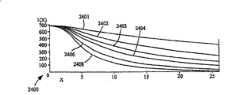
接下来参考图24,所示的是根据本发明的一个实施例的具有不同漫反射系数值的照度图。Referring next to FIG. 24 , shown is a graph of illuminance with different albedo values in accordance with one embodiment of the present invention.
示出的是沿图22中的射出器区213的总长的第一遍镜面照明度I(x)的图2400。曲线2401描述的是漫反射系数Rdiff(x)=0.1的情况,而曲线2402,2403,2404,2406以及2408分别对应系数值0.2,0.3,0.4,0.6以及0.8。在三条曲线右端的I[26]的值代表了那些未提取的又重新从另一端进入扩展器区211的光线。由于这些光线中的一部分将被图20A中的LED芯片203-205所吸收,所以将会有一个返回系数Rexp。返回的光线将与图20c中的扩展器区211射出的光源光线加在一起。这使图24中的每条曲线都乘一个系数Shown is a
F=1+RexpI{26/I[0]}+{RexpI[26]/I[0]}2+...F=1+Rexp I{26/I[0]}+{Rexp I[26]/I[0]}2 +...
=1/{1-RexpI[26]/I[0]}=1/{1-Rexp I[26]/I[0]}
亮度将由从两个扩展器区相乘的照度计算得到:Brightness will be calculated from the illuminance multiplied from the two expander zones:
B(x)=FRdiff(x)[I(x)+I(A-x)]B(x)=FRdiff (x)[I(x)+I(Ax)]
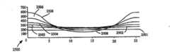
接下来参考图25,所示的是本发明的一个实施例的对不同漫反射系数值的亮度图。Referring next to FIG. 25, shown is a plot of luminance versus albedo values for one embodiment of the present invention.
所示的是图2500的上述计算结果,对应于漫反射率从0.1变化到0.8的亮度曲线2501到2508。曲线2503有最高中心值I(13)。这说明一个好的初始值Rdiff(0)在0.3左右,并往中心有增加的值。Shown are the above calculation results for
接下来参考图26,所示的是根据本发明的一个实施例所示出的漫反射率的线性分布图,该线性分布给出了均匀亮度。Referring next to FIG. 26 , shown is a graph showing a linear distribution of diffuse reflectance that gives uniform brightness in accordance with one embodiment of the present invention.
所示的是可以给出285均匀亮度的一个漫反射率分布。这个结果将会是输出亮度的零阶估值,只有镜面光作为光源光被散射。但被俘获在射出器内部的60%的散射光将沿着内表面增加一个散射亮度ID(x)。根据图23a,在圆周2139外的每一物有散射亮度,包括在图13中扩展器区211上部的卵形区域231。Shown is a diffuse albedo distribution that would give a uniform brightness of 285. The result will be a zero-order estimate of the output luminance, with only specular light being scattered as source light. But the 60% of the scattered light trapped inside the emitter will add a diffuse brightnessID (x) along the inner surface. According to FIG. 23 a , everything outside the
虽然扩展器区211本身并不产生散射,而绝大多数的散射光除了与芯片相关的外进入其内部后都将反射回射出器213。因此漫射照度随x的变化很小,有助于使一阶照度比零阶估值更加平滑。几个更高阶的照度会给照度增加越来越小的数量,因为漫散射的光镜面地来回循环并被散射。因此零阶亮度BT(x)为了使最终的均匀亮度令人满意,并不需要绝对的均匀。Although the
具有校准σ的有关联的以及无关联的粗糙度都可以通过金刚石削处理金属主部件中形成射出器213来获得。这个部件可以用传统制模工艺制成模型。一个较好的金刚石削金属具有校准好的子波长粗糙度的主部件方法是用宽带的白噪声信号带动金刚石工具作振幅为a(x)级的声频振动以提供无关联的粗糙度。Both correlated and uncorrelated roughness with calibration σ can be obtained by forming
尽管这里所公开的发明已经通过具体的实施例和其中的应用加以描述,但是本领域普通技术人员仍可在不超出权利要求提出的范围内做大量修改和变化。Although the invention disclosed here has been described through specific embodiments and applications therein, those skilled in the art can make numerous modifications and changes within the scope not exceeding the scope set forth in the claims.
Claims (19)
Translated fromChineseApplications Claiming Priority (3)
| Application Number | Priority Date | Filing Date | Title |
|---|---|---|---|
| US47069103P | 2003-05-13 | 2003-05-13 | |
| US60/470,691 | 2003-05-13 | ||
| US10/461,557 | 2003-06-12 |
Publications (2)
| Publication Number | Publication Date |
|---|---|
| CN1806336A CN1806336A (en) | 2006-07-19 |
| CN100452424Ctrue CN100452424C (en) | 2009-01-14 |
Family
ID=36867525
Family Applications (1)
| Application Number | Title | Priority Date | Filing Date |
|---|---|---|---|
| CNB2004800169230AExpired - LifetimeCN100452424C (en) | 2003-05-13 | 2004-05-13 | Optical device for LED-based light-bulb substitute |
Country Status (1)
| Country | Link |
|---|---|
| CN (1) | CN100452424C (en) |
Families Citing this family (6)
| Publication number | Priority date | Publication date | Assignee | Title |
|---|---|---|---|---|
| US8449150B2 (en)* | 2009-02-03 | 2013-05-28 | Osram Sylvania Inc. | Tir lens for light emitting diodes |
| DE102009038864B4 (en) | 2009-08-27 | 2021-11-25 | Pictiva Displays International Limited | General lighting lamp |
| CN102695913A (en)* | 2009-10-02 | 2012-09-26 | Ge照明解决方案有限责任公司 | Light emitting diode (LED) based lamp |
| TW201213734A (en)* | 2010-09-20 | 2012-04-01 | zhi-ming You | Light guide pipe for homogenous emission of light and LED light using the light guide pipe |
| RU2645147C2 (en)* | 2012-03-08 | 2018-02-15 | Филипс Лайтинг Холдинг Б.В. | Light-emitting device and method of manufacture of light-emitting device |
| CN105757611B (en)* | 2014-12-18 | 2017-11-17 | 北京欣天和怡机电设备安装工程有限公司 | Double ellipsoid reflector, LED light emission device and light fixtures |
Citations (7)
| Publication number | Priority date | Publication date | Assignee | Title |
|---|---|---|---|---|
| US3760237A (en)* | 1972-06-21 | 1973-09-18 | Gen Electric | Solid state lamp assembly having conical light director |
| US3774021A (en)* | 1972-05-25 | 1973-11-20 | Bell Telephone Labor Inc | Light emitting device |
| US3938177A (en)* | 1973-06-25 | 1976-02-10 | Amp Incorporated | Narrow lead contact for automatic face down bonding of electronic chips |
| US4211955A (en)* | 1978-03-02 | 1980-07-08 | Ray Stephen W | Solid state lamp |
| US4388673A (en)* | 1981-06-22 | 1983-06-14 | Mag Instrument, Inc. | Variable light beam flashlight and recharging unit |
| US4638343A (en)* | 1985-01-04 | 1987-01-20 | Siemens Aktiengesellschaft | Optical radiation source or detector device having plural radiating or receiving characteristics |
| US5865529A (en)* | 1997-03-10 | 1999-02-02 | Yan; Ellis | Light emitting diode lamp having a spherical radiating pattern |
- 2004
- 2004-05-13CNCNB2004800169230Apatent/CN100452424C/ennot_activeExpired - Lifetime
Patent Citations (7)
| Publication number | Priority date | Publication date | Assignee | Title |
|---|---|---|---|---|
| US3774021A (en)* | 1972-05-25 | 1973-11-20 | Bell Telephone Labor Inc | Light emitting device |
| US3760237A (en)* | 1972-06-21 | 1973-09-18 | Gen Electric | Solid state lamp assembly having conical light director |
| US3938177A (en)* | 1973-06-25 | 1976-02-10 | Amp Incorporated | Narrow lead contact for automatic face down bonding of electronic chips |
| US4211955A (en)* | 1978-03-02 | 1980-07-08 | Ray Stephen W | Solid state lamp |
| US4388673A (en)* | 1981-06-22 | 1983-06-14 | Mag Instrument, Inc. | Variable light beam flashlight and recharging unit |
| US4638343A (en)* | 1985-01-04 | 1987-01-20 | Siemens Aktiengesellschaft | Optical radiation source or detector device having plural radiating or receiving characteristics |
| US5865529A (en)* | 1997-03-10 | 1999-02-02 | Yan; Ellis | Light emitting diode lamp having a spherical radiating pattern |
Also Published As
| Publication number | Publication date |
|---|---|
| CN1806336A (en) | 2006-07-19 |
Similar Documents
| Publication | Publication Date | Title |
|---|---|---|
| US20230135796A1 (en) | Light-Emitting Devices Providing Asymmetrical Propagation of Light | |
| EP1634335B1 (en) | Optical device for led-based light-bulb substitute | |
| US8866168B2 (en) | Optical devices for controlled color mixing | |
| TWI249257B (en) | Illumination apparatus | |
| CN101900302B (en) | For the beam spreading optics of light emitting diode | |
| TWI576541B (en) | Compact light-mixing led light engine and white led lamp with narrow beam and high cri using same | |
| US8038319B2 (en) | Luminaire and method of operation | |
| CN105723530B (en) | Light emitting device and lighting device integrating the same | |
| US7181378B2 (en) | Compact folded-optics illumination lens | |
| US12234984B2 (en) | Lens for improved color mixing and beam control of an LED light source | |
| EP2721656B1 (en) | Led light source | |
| US12253661B2 (en) | Total internal reflection lens to improve color mixing of an LED light source | |
| US20160195243A1 (en) | Optical system for producing uniform illumination | |
| US20080123349A1 (en) | Optical device for led-based lamp | |
| CN100452424C (en) | Optical device for LED-based light-bulb substitute | |
| CA3061625C (en) | Total internal reflection lens to lessen glare and maintain color mixing and beam control | |
| CN101203965B (en) | Lighting device and method for lighting device design |
Legal Events
| Date | Code | Title | Description |
|---|---|---|---|
| C06 | Publication | ||
| PB01 | Publication | ||
| C10 | Entry into substantive examination | ||
| SE01 | Entry into force of request for substantive examination | ||
| C14 | Grant of patent or utility model | ||
| GR01 | Patent grant | ||
| ASS | Succession or assignment of patent right | Owner name:LIGHT ENGINE LTD. Free format text:FORMER OWNER: LIGHT PRESCRIPTIONS INNOVATORS Effective date:20121017 | |
| C41 | Transfer of patent application or patent right or utility model | ||
| COR | Change of bibliographic data | Free format text:CORRECT: ADDRESS; TO: HONG KONG, CHINA | |
| TR01 | Transfer of patent right | Effective date of registration:20121017 Address after:Floor 6, optoelectronics centre, 2 East Science Avenue, Sha Tin Hongkong Science Park, Hongkong, China Patentee after:LIGHT ENGINE Ltd. Address before:California, USA Patentee before:LIGHT PRESCRIPTIONS INNOVATORS, LLC | |
| CX01 | Expiry of patent term | ||
| CX01 | Expiry of patent term | Granted publication date:20090114 |