CN100449800C - Semiconductor substrates and semiconductor devices manufactured by epitaxial growth on semiconductor substrates - Google Patents
Semiconductor substrates and semiconductor devices manufactured by epitaxial growth on semiconductor substratesDownload PDFInfo
- Publication number
- CN100449800C CN100449800CCNB2005100977489ACN200510097748ACN100449800CCN 100449800 CCN100449800 CCN 100449800CCN B2005100977489 ACNB2005100977489 ACN B2005100977489ACN 200510097748 ACN200510097748 ACN 200510097748ACN 100449800 CCN100449800 CCN 100449800C
- Authority
- CN
- China
- Prior art keywords
- layer
- type
- iii
- semiconductor device
- gan substrate
- Prior art date
- Legal status (The legal status is an assumption and is not a legal conclusion. Google has not performed a legal analysis and makes no representation as to the accuracy of the status listed.)
- Expired - Lifetime
Links
Images


Classifications
- H—ELECTRICITY
- H10—SEMICONDUCTOR DEVICES; ELECTRIC SOLID-STATE DEVICES NOT OTHERWISE PROVIDED FOR
- H10H—INORGANIC LIGHT-EMITTING SEMICONDUCTOR DEVICES HAVING POTENTIAL BARRIERS
- H10H20/00—Individual inorganic light-emitting semiconductor devices having potential barriers, e.g. light-emitting diodes [LED]
- H10H20/80—Constructional details
- H10H20/81—Bodies
- H10H20/822—Materials of the light-emitting regions
- H10H20/824—Materials of the light-emitting regions comprising only Group III-V materials, e.g. GaP
- H10H20/825—Materials of the light-emitting regions comprising only Group III-V materials, e.g. GaP containing nitrogen, e.g. GaN
- H—ELECTRICITY
- H01—ELECTRIC ELEMENTS
- H01L—SEMICONDUCTOR DEVICES NOT COVERED BY CLASS H10
- H01L21/00—Processes or apparatus adapted for the manufacture or treatment of semiconductor or solid state devices or of parts thereof
- H01L21/02—Manufacture or treatment of semiconductor devices or of parts thereof
- H01L21/04—Manufacture or treatment of semiconductor devices or of parts thereof the devices having potential barriers, e.g. a PN junction, depletion layer or carrier concentration layer
- H01L21/18—Manufacture or treatment of semiconductor devices or of parts thereof the devices having potential barriers, e.g. a PN junction, depletion layer or carrier concentration layer the devices having semiconductor bodies comprising elements of Group IV of the Periodic Table or AIIIBV compounds with or without impurities, e.g. doping materials
- H01L21/20—Deposition of semiconductor materials on a substrate, e.g. epitaxial growth solid phase epitaxy
- C—CHEMISTRY; METALLURGY
- C30—CRYSTAL GROWTH
- C30B—SINGLE-CRYSTAL GROWTH; UNIDIRECTIONAL SOLIDIFICATION OF EUTECTIC MATERIAL OR UNIDIRECTIONAL DEMIXING OF EUTECTOID MATERIAL; REFINING BY ZONE-MELTING OF MATERIAL; PRODUCTION OF A HOMOGENEOUS POLYCRYSTALLINE MATERIAL WITH DEFINED STRUCTURE; SINGLE CRYSTALS OR HOMOGENEOUS POLYCRYSTALLINE MATERIAL WITH DEFINED STRUCTURE; AFTER-TREATMENT OF SINGLE CRYSTALS OR A HOMOGENEOUS POLYCRYSTALLINE MATERIAL WITH DEFINED STRUCTURE; APPARATUS THEREFOR
- C30B25/00—Single-crystal growth by chemical reaction of reactive gases, e.g. chemical vapour-deposition growth
- C30B25/02—Epitaxial-layer growth
- C30B25/18—Epitaxial-layer growth characterised by the substrate
- C30B25/20—Epitaxial-layer growth characterised by the substrate the substrate being of the same materials as the epitaxial layer
- C—CHEMISTRY; METALLURGY
- C30—CRYSTAL GROWTH
- C30B—SINGLE-CRYSTAL GROWTH; UNIDIRECTIONAL SOLIDIFICATION OF EUTECTIC MATERIAL OR UNIDIRECTIONAL DEMIXING OF EUTECTOID MATERIAL; REFINING BY ZONE-MELTING OF MATERIAL; PRODUCTION OF A HOMOGENEOUS POLYCRYSTALLINE MATERIAL WITH DEFINED STRUCTURE; SINGLE CRYSTALS OR HOMOGENEOUS POLYCRYSTALLINE MATERIAL WITH DEFINED STRUCTURE; AFTER-TREATMENT OF SINGLE CRYSTALS OR A HOMOGENEOUS POLYCRYSTALLINE MATERIAL WITH DEFINED STRUCTURE; APPARATUS THEREFOR
- C30B29/00—Single crystals or homogeneous polycrystalline material with defined structure characterised by the material or by their shape
- C30B29/10—Inorganic compounds or compositions
- C30B29/40—AIIIBV compounds wherein A is B, Al, Ga, In or Tl and B is N, P, As, Sb or Bi
- C30B29/403—AIII-nitrides
- C30B29/406—Gallium nitride
- H—ELECTRICITY
- H01—ELECTRIC ELEMENTS
- H01L—SEMICONDUCTOR DEVICES NOT COVERED BY CLASS H10
- H01L21/00—Processes or apparatus adapted for the manufacture or treatment of semiconductor or solid state devices or of parts thereof
- H01L21/02—Manufacture or treatment of semiconductor devices or of parts thereof
- H01L21/02104—Forming layers
- H01L21/02365—Forming inorganic semiconducting materials on a substrate
- H01L21/02367—Substrates
- H01L21/0237—Materials
- H01L21/02387—Group 13/15 materials
- H01L21/02389—Nitrides
- H—ELECTRICITY
- H01—ELECTRIC ELEMENTS
- H01L—SEMICONDUCTOR DEVICES NOT COVERED BY CLASS H10
- H01L21/00—Processes or apparatus adapted for the manufacture or treatment of semiconductor or solid state devices or of parts thereof
- H01L21/02—Manufacture or treatment of semiconductor devices or of parts thereof
- H01L21/02104—Forming layers
- H01L21/02365—Forming inorganic semiconducting materials on a substrate
- H01L21/02367—Substrates
- H01L21/02433—Crystal orientation
- H—ELECTRICITY
- H01—ELECTRIC ELEMENTS
- H01L—SEMICONDUCTOR DEVICES NOT COVERED BY CLASS H10
- H01L21/00—Processes or apparatus adapted for the manufacture or treatment of semiconductor or solid state devices or of parts thereof
- H01L21/02—Manufacture or treatment of semiconductor devices or of parts thereof
- H01L21/02104—Forming layers
- H01L21/02365—Forming inorganic semiconducting materials on a substrate
- H01L21/02436—Intermediate layers between substrates and deposited layers
- H01L21/02439—Materials
- H01L21/02455—Group 13/15 materials
- H01L21/02458—Nitrides
- H—ELECTRICITY
- H01—ELECTRIC ELEMENTS
- H01L—SEMICONDUCTOR DEVICES NOT COVERED BY CLASS H10
- H01L21/00—Processes or apparatus adapted for the manufacture or treatment of semiconductor or solid state devices or of parts thereof
- H01L21/02—Manufacture or treatment of semiconductor devices or of parts thereof
- H01L21/02104—Forming layers
- H01L21/02365—Forming inorganic semiconducting materials on a substrate
- H01L21/02436—Intermediate layers between substrates and deposited layers
- H01L21/02494—Structure
- H01L21/02496—Layer structure
- H01L21/02505—Layer structure consisting of more than two layers
- H01L21/02507—Alternating layers, e.g. superlattice
- H—ELECTRICITY
- H01—ELECTRIC ELEMENTS
- H01L—SEMICONDUCTOR DEVICES NOT COVERED BY CLASS H10
- H01L21/00—Processes or apparatus adapted for the manufacture or treatment of semiconductor or solid state devices or of parts thereof
- H01L21/02—Manufacture or treatment of semiconductor devices or of parts thereof
- H01L21/02104—Forming layers
- H01L21/02365—Forming inorganic semiconducting materials on a substrate
- H01L21/02518—Deposited layers
- H01L21/02521—Materials
- H01L21/02538—Group 13/15 materials
- H01L21/0254—Nitrides
- H—ELECTRICITY
- H01—ELECTRIC ELEMENTS
- H01L—SEMICONDUCTOR DEVICES NOT COVERED BY CLASS H10
- H01L21/00—Processes or apparatus adapted for the manufacture or treatment of semiconductor or solid state devices or of parts thereof
- H01L21/02—Manufacture or treatment of semiconductor devices or of parts thereof
- H01L21/02104—Forming layers
- H01L21/02365—Forming inorganic semiconducting materials on a substrate
- H01L21/02518—Deposited layers
- H01L21/0257—Doping during depositing
- H01L21/02573—Conductivity type
- H01L21/02576—N-type
- H—ELECTRICITY
- H01—ELECTRIC ELEMENTS
- H01L—SEMICONDUCTOR DEVICES NOT COVERED BY CLASS H10
- H01L21/00—Processes or apparatus adapted for the manufacture or treatment of semiconductor or solid state devices or of parts thereof
- H01L21/02—Manufacture or treatment of semiconductor devices or of parts thereof
- H01L21/02104—Forming layers
- H01L21/02365—Forming inorganic semiconducting materials on a substrate
- H01L21/02518—Deposited layers
- H01L21/0257—Doping during depositing
- H01L21/02584—Delta-doping
- H—ELECTRICITY
- H01—ELECTRIC ELEMENTS
- H01L—SEMICONDUCTOR DEVICES NOT COVERED BY CLASS H10
- H01L21/00—Processes or apparatus adapted for the manufacture or treatment of semiconductor or solid state devices or of parts thereof
- H01L21/02—Manufacture or treatment of semiconductor devices or of parts thereof
- H01L21/02104—Forming layers
- H01L21/02365—Forming inorganic semiconducting materials on a substrate
- H01L21/02612—Formation types
- H01L21/02617—Deposition types
- H01L21/0262—Reduction or decomposition of gaseous compounds, e.g. CVD
- H—ELECTRICITY
- H10—SEMICONDUCTOR DEVICES; ELECTRIC SOLID-STATE DEVICES NOT OTHERWISE PROVIDED FOR
- H10D—INORGANIC ELECTRIC SEMICONDUCTOR DEVICES
- H10D30/00—Field-effect transistors [FET]
- H10D30/40—FETs having zero-dimensional [0D], one-dimensional [1D] or two-dimensional [2D] charge carrier gas channels
- H10D30/47—FETs having zero-dimensional [0D], one-dimensional [1D] or two-dimensional [2D] charge carrier gas channels having 2D charge carrier gas channels, e.g. nanoribbon FETs or high electron mobility transistors [HEMT]
- H10D30/471—High electron mobility transistors [HEMT] or high hole mobility transistors [HHMT]
- H10D30/475—High electron mobility transistors [HEMT] or high hole mobility transistors [HHMT] having wider bandgap layer formed on top of lower bandgap active layer, e.g. undoped barrier HEMTs such as i-AlGaN/GaN HEMTs
- H10D30/4755—High electron mobility transistors [HEMT] or high hole mobility transistors [HHMT] having wider bandgap layer formed on top of lower bandgap active layer, e.g. undoped barrier HEMTs such as i-AlGaN/GaN HEMTs having wide bandgap charge-carrier supplying layers, e.g. modulation doped HEMTs such as n-AlGaAs/GaAs HEMTs
- H—ELECTRICITY
- H10—SEMICONDUCTOR DEVICES; ELECTRIC SOLID-STATE DEVICES NOT OTHERWISE PROVIDED FOR
- H10D—INORGANIC ELECTRIC SEMICONDUCTOR DEVICES
- H10D30/00—Field-effect transistors [FET]
- H10D30/80—FETs having rectifying junction gate electrodes
- H10D30/87—FETs having Schottky gate electrodes, e.g. metal-semiconductor FETs [MESFET]
- H—ELECTRICITY
- H10—SEMICONDUCTOR DEVICES; ELECTRIC SOLID-STATE DEVICES NOT OTHERWISE PROVIDED FOR
- H10D—INORGANIC ELECTRIC SEMICONDUCTOR DEVICES
- H10D62/00—Semiconductor bodies, or regions thereof, of devices having potential barriers
- H10D62/40—Crystalline structures
- H10D62/405—Orientations of crystalline planes
- H—ELECTRICITY
- H10—SEMICONDUCTOR DEVICES; ELECTRIC SOLID-STATE DEVICES NOT OTHERWISE PROVIDED FOR
- H10D—INORGANIC ELECTRIC SEMICONDUCTOR DEVICES
- H10D62/00—Semiconductor bodies, or regions thereof, of devices having potential barriers
- H10D62/80—Semiconductor bodies, or regions thereof, of devices having potential barriers characterised by the materials
- H10D62/82—Heterojunctions
- H10D62/824—Heterojunctions comprising only Group III-V materials heterojunctions, e.g. GaN/AlGaN heterojunctions
- H—ELECTRICITY
- H10—SEMICONDUCTOR DEVICES; ELECTRIC SOLID-STATE DEVICES NOT OTHERWISE PROVIDED FOR
- H10D—INORGANIC ELECTRIC SEMICONDUCTOR DEVICES
- H10D8/00—Diodes
- H—ELECTRICITY
- H10—SEMICONDUCTOR DEVICES; ELECTRIC SOLID-STATE DEVICES NOT OTHERWISE PROVIDED FOR
- H10H—INORGANIC LIGHT-EMITTING SEMICONDUCTOR DEVICES HAVING POTENTIAL BARRIERS
- H10H20/00—Individual inorganic light-emitting semiconductor devices having potential barriers, e.g. light-emitting diodes [LED]
- H10H20/01—Manufacture or treatment
- H10H20/011—Manufacture or treatment of bodies, e.g. forming semiconductor layers
- H10H20/013—Manufacture or treatment of bodies, e.g. forming semiconductor layers having light-emitting regions comprising only Group III-V materials
- H10H20/0137—Manufacture or treatment of bodies, e.g. forming semiconductor layers having light-emitting regions comprising only Group III-V materials the light-emitting regions comprising nitride materials
- H—ELECTRICITY
- H10—SEMICONDUCTOR DEVICES; ELECTRIC SOLID-STATE DEVICES NOT OTHERWISE PROVIDED FOR
- H10H—INORGANIC LIGHT-EMITTING SEMICONDUCTOR DEVICES HAVING POTENTIAL BARRIERS
- H10H20/00—Individual inorganic light-emitting semiconductor devices having potential barriers, e.g. light-emitting diodes [LED]
- H10H20/80—Constructional details
- H10H20/81—Bodies
- H10H20/817—Bodies characterised by the crystal structures or orientations, e.g. polycrystalline, amorphous or porous
- H—ELECTRICITY
- H01—ELECTRIC ELEMENTS
- H01S—DEVICES USING THE PROCESS OF LIGHT AMPLIFICATION BY STIMULATED EMISSION OF RADIATION [LASER] TO AMPLIFY OR GENERATE LIGHT; DEVICES USING STIMULATED EMISSION OF ELECTROMAGNETIC RADIATION IN WAVE RANGES OTHER THAN OPTICAL
- H01S5/00—Semiconductor lasers
- H01S5/30—Structure or shape of the active region; Materials used for the active region
- H01S5/32—Structure or shape of the active region; Materials used for the active region comprising PN junctions, e.g. hetero- or double- heterostructures
- H01S5/3202—Structure or shape of the active region; Materials used for the active region comprising PN junctions, e.g. hetero- or double- heterostructures grown on specifically orientated substrates, or using orientation dependent growth
- H01S5/320275—Structure or shape of the active region; Materials used for the active region comprising PN junctions, e.g. hetero- or double- heterostructures grown on specifically orientated substrates, or using orientation dependent growth semi-polar orientation
- H—ELECTRICITY
- H01—ELECTRIC ELEMENTS
- H01S—DEVICES USING THE PROCESS OF LIGHT AMPLIFICATION BY STIMULATED EMISSION OF RADIATION [LASER] TO AMPLIFY OR GENERATE LIGHT; DEVICES USING STIMULATED EMISSION OF ELECTROMAGNETIC RADIATION IN WAVE RANGES OTHER THAN OPTICAL
- H01S5/00—Semiconductor lasers
- H01S5/30—Structure or shape of the active region; Materials used for the active region
- H01S5/32—Structure or shape of the active region; Materials used for the active region comprising PN junctions, e.g. hetero- or double- heterostructures
- H01S5/323—Structure or shape of the active region; Materials used for the active region comprising PN junctions, e.g. hetero- or double- heterostructures in AIIIBV compounds, e.g. AlGaAs-laser, InP-based laser
- H01S5/32308—Structure or shape of the active region; Materials used for the active region comprising PN junctions, e.g. hetero- or double- heterostructures in AIIIBV compounds, e.g. AlGaAs-laser, InP-based laser emitting light at a wavelength less than 900 nm
- H01S5/32341—Structure or shape of the active region; Materials used for the active region comprising PN junctions, e.g. hetero- or double- heterostructures in AIIIBV compounds, e.g. AlGaAs-laser, InP-based laser emitting light at a wavelength less than 900 nm blue laser based on GaN or GaP
- H—ELECTRICITY
- H10—SEMICONDUCTOR DEVICES; ELECTRIC SOLID-STATE DEVICES NOT OTHERWISE PROVIDED FOR
- H10D—INORGANIC ELECTRIC SEMICONDUCTOR DEVICES
- H10D62/00—Semiconductor bodies, or regions thereof, of devices having potential barriers
- H10D62/80—Semiconductor bodies, or regions thereof, of devices having potential barriers characterised by the materials
- H10D62/85—Semiconductor bodies, or regions thereof, of devices having potential barriers characterised by the materials being Group III-V materials, e.g. GaAs
- H10D62/8503—Nitride Group III-V materials, e.g. AlN or GaN
Landscapes
- Engineering & Computer Science (AREA)
- Chemical & Material Sciences (AREA)
- Microelectronics & Electronic Packaging (AREA)
- General Physics & Mathematics (AREA)
- Manufacturing & Machinery (AREA)
- Computer Hardware Design (AREA)
- Power Engineering (AREA)
- Condensed Matter Physics & Semiconductors (AREA)
- Physics & Mathematics (AREA)
- Crystallography & Structural Chemistry (AREA)
- Materials Engineering (AREA)
- Organic Chemistry (AREA)
- Metallurgy (AREA)
- General Chemical & Material Sciences (AREA)
- Chemical Kinetics & Catalysis (AREA)
- Inorganic Chemistry (AREA)
- Semiconductor Lasers (AREA)
- Led Devices (AREA)
- Bipolar Transistors (AREA)
- Junction Field-Effect Transistors (AREA)
- Crystals, And After-Treatments Of Crystals (AREA)
- Recrystallisation Techniques (AREA)
Abstract
Translated fromChineseDescription
Translated fromChinese相关申请的交叉引用Cross References to Related Applications
本申请权利要求基于2004年8月24日递交的日本专利申请第P2004-244072号的35USC 119下的优先权,该专利申请的全部内容引入本文作参考。The claims of this application are based on the priority under 35USC 119 of Japanese Patent Application No. P2004-244072 submitted on August 24, 2004, and the entire content of this patent application is incorporated herein as a reference.
技术领域technical field
本发明涉及一种包括大块GaN衬底和大块GaN衬底上的外延生长层的半导体衬底,或者外延衬底,以及通过在所述半导体衬底上外延生长所实现的半导体器件。此处,半导体器件包括各种半导体光学器件,例如半导体发光器件和各种半导体电子器件,例如晶体管。The present invention relates to a semiconductor substrate comprising a bulk GaN substrate and an epitaxial growth layer on the bulk GaN substrate, or an epitaxial substrate, and a semiconductor device realized by epitaxial growth on the semiconductor substrate. Here, the semiconductor device includes various semiconductor optical devices such as semiconductor light emitting devices and various semiconductor electronic devices such as transistors.
背景技术Background technique
III-V族氮化物化合物半导体,例如氮化镓(GaN)具有宽的带隙。已经研究并开发了宽带隙半导体、高亮度紫外-蓝/绿光发二极管(LEDs)和蓝紫光激光二极管等的使用性质和特征。另外,已经基于宽带隙半导体的性质和特征制造出高频/大功率III-V族氮化物化合物半导体场效应晶体管(FETs)等。Group III-V nitride compound semiconductors, such as gallium nitride (GaN), have a wide bandgap. The usage properties and characteristics of wide-bandgap semiconductors, high-brightness ultraviolet-blue/green light-emitting diodes (LEDs), and blue-violet laser diodes have been researched and developed. In addition, high frequency/high power group III-V nitride compound semiconductor field effect transistors (FETs) and the like have been fabricated based on the properties and characteristics of wide bandgap semiconductors.
因为在研究和开发的早期阶段还没有在III-V族氮化物化合物半导体的晶体生长中允许晶格匹配的衬底,所以使用蓝宝石(Al2O3)、碳化硅(SiC)等作为衬底,通过晶体生长来制造半导体器件。对于使用Al2O3衬底的III-V族氮化物化合物半导体的晶体生长,使用两步生长方法。但是,使用这种方法,由于在Al2O3和III-V族氮化物化合物半导体之间存在晶格常数和热膨胀系数的差异,所以产生了大量的引线错位和缺陷。因为它们会缩短激光二极管的寿命,例如不良的可靠性,所以这些引线错位和缺陷是实际使用期间的主要问题。Since there was no substrate allowing lattice matching in the crystal growth of III-V nitride compound semiconductors in the early stages of research and development, sapphire (Al2 O3 ), silicon carbide (SiC), etc. were used as substrates , to manufacture semiconductor devices by crystal growth. For the crystal growth of group III-V nitride compound semiconductors usingAl2O3 substrates, a two- step growth method was used. However, with this method, a large number of wire dislocations and defects are generated due to differences in lattice constant and thermal expansioncoefficient betweenAl2O3 and III-V nitride compound semiconductors. These lead misalignments and defects are a major problem during practical use because they shorten the life of the laser diode, eg, poor reliability.
因此,向市场提供在其上面可以实现均匀的外延生长的大块GaN衬底已经是期待已久的需求。由于最近在晶体生长技术方面的进展,已经可以获得大块GaN衬底,并且已经报道了制造原型InGaN/GaN/AlGaN基激光二极管的结果(参阅S.Nakamura等,Continuous-wave operation of InGaN/GaN/AlGaN-based laser diodesgrown on GaN substrates,Applied Physics Letters,第72卷,第2期,第2014-2016页,4月20日,1998年)。Therefore, it has been a long-awaited demand to provide the market with a bulk GaN substrate on which uniform epitaxial growth can be achieved. Thanks to recent advances in crystal growth techniques, bulk GaN substrates have been obtained and results have been reported for the fabrication of prototype InGaN/GaN/AlGaN-based laser diodes (see S. Nakamura et al., Continuous-wave operation of InGaN/GaN / AlGaN-based laser diodes grown on GaN substrates, Applied Physics Letters, Vol. 72, No. 2, Pages 2014-2016, April 20, 1998).
但是,关于大块GaN衬底自身或者在大块GaN衬底上的均匀外延生长知之甚少,并且仍然没有建立使用III-V族氮化物化合物半导体制造半导体器件,例如高性能的半导体光学器件或高性能的半导体电子器件的方法。However, little is known about bulk GaN substrates themselves or uniform epitaxial growth on bulk GaN substrates, and the use of III-V nitride compound semiconductors to fabricate semiconductor devices, such as high-performance semiconductor optical devices or A method for high performance semiconductor electronic devices.
发明内容Contents of the invention
从这些情况来看,本发明的目的是提供一种半导体衬底或外延衬底,其包括大块GaN衬底(下文称作“GaN衬底”)和GaN衬底上的外延生长层,所述外延生长层具有半导体器件尺寸所需的改善的表面平整度,以及一种通过在所述半导体衬底(外延衬底)上外延生长而实现的高性能的半导体器件。In view of these circumstances, an object of the present invention is to provide a semiconductor substrate or an epitaxial substrate comprising a bulk GaN substrate (hereinafter referred to as "GaN substrate") and an epitaxially grown layer on the GaN substrate, so that The epitaxial growth layer has improved surface flatness required for the size of a semiconductor device, and a high-performance semiconductor device realized by epitaxial growth on the semiconductor substrate (epitaxial substrate).
为了实现上述目的,本发明的一个方面其特征在于一种半导体衬底,其包括GaN衬底,其表面取向由位于0.12度至0.35度范围内的从{0001}面向<1-100>方向的表面倾角绝对值和位于0.00度至0.06度范围内的从{0001}面向<11-20>方向的表面倾角绝对值来定义,以及在GaN衬底表面上外延生长的由III-V族氮化物化合物半导体组成的单晶层。In order to achieve the above object, an aspect of the present invention is characterized by a semiconductor substrate comprising a GaN substrate whose surface orientation consists of a direction from {0001} facing the <1-100> direction in the range of 0.12 degrees to 0.35 degrees. The absolute value of the surface tilt angle and the absolute value of the surface tilt angle from {0001} facing the <11-20> direction in the range of 0.00 degrees to 0.06 degrees, and the epitaxially grown III-V nitrides on the surface of the GaN substrate A single crystal layer composed of compound semiconductors.
本发明的另一个方面其特征在于一种半导体发光器件,其包括:GaN衬底,其表面取向由位于0.12度至0.35度范围内的从{0001}面向<1-100>方向的表面倾角绝对值和位于0.00度至0.06度范围内的从{0001}面向<11-20>方向的表面倾角绝对值来定义;在GaN衬底表面上外延生长的由III-V族氮化物化合物半导体组成的单晶层;以及在所述单晶层上提供的由外延生长的III-V族氮化物化合物半导体组成的发光层。Another aspect of the present invention is characterized by a semiconductor light emitting device comprising: a GaN substrate whose surface orientation is determined by a surface tilt angle absolute value and the absolute value of the surface inclination angle from {0001} facing the <11-20> direction in the range of 0.00 degrees to 0.06 degrees; the epitaxial growth on the surface of the GaN substrate is composed of III-V nitride compound semiconductors a single crystal layer; and a light emitting layer composed of an epitaxially grown Group III-V nitride compound semiconductor provided on the single crystal layer.
本发明的再另一个方面其特征在于一种半导体器件,其包括:GaN衬底,其表面取向由位于0.12度至0.35度范围内的从{0001}面向<1-100>方向的表面倾角绝对值和位于0.00度至0.06度范围内的从{0001}面表面向<11-20>方向的倾角绝对值来定义;以及在GaN衬底上提供的由外延生长的III-V族氮化物化合物半导体组成的器件结构部分。Still another aspect of the present invention is characterized by a semiconductor device comprising: a GaN substrate whose surface orientation is defined by a surface tilt angle absolute from {0001} facing the <1-100> direction in the range of 0.12 degrees to 0.35 degrees. value and the absolute value of the inclination angle from the {0001} plane surface to the <11-20> direction in the range of 0.00 degrees to 0.06 degrees; and the epitaxially grown III-V nitride compound provided on a GaN substrate The structural part of a device composed of semiconductors.
附图说明Description of drawings
图1是表示根据本发明第一实施方案的半导体器件(激光二极管)的剖面结构的示意图;1 is a schematic diagram showing a cross-sectional structure of a semiconductor device (laser diode) according to a first embodiment of the present invention;
图2是表示根据本发明第一实施方案,半导体器件(激光二极管)在25℃和连续振荡条件下的电流对光输出功率特性的图,该图与相同条件下比较实施例的电流对光输出功率的特性进行了比较;Fig. 2 is a graph showing the current-to-light output power characteristics of a semiconductor device (laser diode) at 25°C and continuous oscillation conditions according to the first embodiment of the present invention, which is compared with the current-to-light output of the comparative example under the same conditions power characteristics were compared;
图3A表示根据本发明的第一实施方案,通过ω/2θ扫描通过用于半导体器件的堆叠结构的(0002)面所获得的X射线衍射图,所述堆叠结构连续外延生长在所述GaN衬底上,其满足由倾角Δθ1-100和Δθ11-20定义的特定表面取向;3A shows an X-ray diffraction pattern obtained by ω/2θ scanning through the (0002) plane of a stack structure for a semiconductor device continuously epitaxially grown on the GaN substrate according to the first embodiment of the present invention. On the bottom, it satisfies a specific surface orientation defined by the dip angles Δθ1-100 and Δθ11-20 ;
图3B表示根据比较实施方案,通过ω/2θ扫描通过用于半导体器件的堆叠结构的(0002)面所获得的X射线衍射图,所述堆叠结构连续外延生长在所述GaN衬底上,其不满足所述特定的表面取向;3B shows an X-ray diffraction pattern obtained by ω/2θ scanning through the (0002) plane of a stack structure for a semiconductor device continuously epitaxially grown on the GaN substrate, according to a comparative embodiment. does not meet the specified surface orientation;
图4是使用多个具有各种晶面方向的GaN衬底,通过绘制从{0001}面向[1-100]方向的倾角Δθ1-100沿着横坐标的绝对值和从{0001}面向[11-20]方向的倾角Δθ11-20沿着纵坐标的绝对值,表示各种外延生长的堆叠结构的表面形貌图,检查该图是为了确定根据本发明第一实施方案的半导体器件的最优条件。Figure 4 uses multiple GaN substrates with various crystal plane orientations, by plotting the absolute value of the inclination angle Δθ1-100 along the abscissa from the {0001} plane to the [1-100] direction and from the {0001} plane to the [1-100] direction. 11-20] The absolute value of the inclination angle Δθ in the direction of11-20 along the ordinate represents a surface topography diagram of various epitaxially grown stacked structures, which is checked in order to determine the performance of the semiconductor device according to the first embodiment of the present invention. optimal conditions.
图5A是表示根据本发明第一实施方案的半导体器件中间产品的工艺流程剖视图,该图解释根据第一实施方案的半导体器件的制造方法;5A is a sectional view showing a process flow of an intermediate product of a semiconductor device according to a first embodiment of the present invention, which explains a method of manufacturing a semiconductor device according to the first embodiment;
图5B是表示图5A所示的工艺阶段后,根据第一实施方案的半导体器件中间产品的后续工艺流程剖视图,该图解释根据第一实施方案的半导体器件的制造方法;5B is a cross-sectional view showing the subsequent process flow of the intermediate product of the semiconductor device according to the first embodiment after the process stage shown in FIG. 5A, which explains the method of manufacturing the semiconductor device according to the first embodiment;
图5C是表示图5B所示的工艺阶段后,根据第一实施方案的半导体器件中间产品的后续工艺流程剖视图,所述中间产品用作第一实施方案的特殊半导体衬底(外延衬底),该图解释根据第一实施方案的半导体器件的制造方法;5C is a cross-sectional view showing the subsequent process flow of the intermediate product of the semiconductor device according to the first embodiment after the process stage shown in FIG. 5B, which is used as the special semiconductor substrate (epitaxial substrate) of the first embodiment This figure explains the manufacturing method of the semiconductor device according to the first embodiment;
图6是表示图5C所示的工艺阶段后,根据第一实施方案的半导体器件中间产品的进一步后续工艺流程剖视图,其中在所述特殊半导体衬底(外延衬底)上连续生长了多个外延层,该图解释根据第一实施方案的半导体器件的制造方法;6 is a cross-sectional view showing a further subsequent process flow of the intermediate product of the semiconductor device according to the first embodiment after the process stage shown in FIG. layer, which explains the method of manufacturing the semiconductor device according to the first embodiment;
图7是表示图6所示的工艺阶段后,根据第一实施方案的半导体器件中间产品的再进一步后续工艺流程剖视图,其中在连续生长在所述特殊半导体衬底(外延衬底)上的堆叠外延层的顶部上形成了脊结构,该图解释根据第一实施方案的半导体器件的制造方法;7 is a cross-sectional view showing a still further subsequent process flow of the intermediate product of the semiconductor device according to the first embodiment after the process stage shown in FIG. A ridge structure is formed on top of the epitaxial layer, this figure explains the method of manufacturing the semiconductor device according to the first embodiment;
图8是表示图7所示的工艺阶段后,根据第一实施方案的半导体器件中间产品的再进一步后续工艺流程剖视图,该图解释根据第一实施方案的半导体器件的制造方法;8 is a cross-sectional view showing a still further subsequent process flow of the intermediate product of the semiconductor device according to the first embodiment after the process stage shown in FIG. 7, which explains the method of manufacturing the semiconductor device according to the first embodiment;
图9是表示图8所示的工艺阶段后,根据第一实施方案的半导体器件中间产品的再进一步后续工艺流程剖视图,该图解释根据第一实施方案的半导体器件的制造方法;FIG. 9 is a sectional view showing a still further subsequent process flow of the intermediate product of the semiconductor device according to the first embodiment after the process stage shown in FIG. 8, which explains the method of manufacturing the semiconductor device according to the first embodiment;
图10是表示图9所示的工艺阶段后,根据第一实施方案的半导体器件中间产品的再进一步后续工艺流程剖视图,该图解释根据第一实施方案的半导体器件的制造方法;10 is a cross-sectional view showing a still further subsequent process flow of the intermediate product of the semiconductor device according to the first embodiment after the process stage shown in FIG. 9, which explains the method of manufacturing the semiconductor device according to the first embodiment;
图11是表示根据本发明第一实施方案的改进,半导体器件(激光二极管)的剖面结构的示意图;11 is a schematic view showing a cross-sectional structure of a semiconductor device (laser diode) according to a modification of the first embodiment of the present invention;
图12是表示根据第一实施方案改进的半导体器件中间产品的工艺流程剖视图,其中在特殊半导体衬底(外延衬底)上连续生长了多个外延层,该图解释根据第一实施方案改进的半导体器件的制造方法;12 is a cross-sectional view showing the process flow of an intermediate product of a semiconductor device according to the first embodiment, wherein a plurality of epitaxial layers are continuously grown on a special semiconductor substrate (epitaxial substrate), which explains the improvement according to the first embodiment. A method of manufacturing a semiconductor device;
图13是表示根据本发明第二实施方案,半导体器件(LED)的剖面结构的示意图;13 is a schematic diagram showing a cross-sectional structure of a semiconductor device (LED) according to a second embodiment of the present invention;
图14是表示根据第二实施方案的半导体器件中间产品的工艺流程剖视图,其中在特殊半导体衬底(外延衬底)上连续生长了多个外延层,该图解释根据第二实施方案的半导体器件的制造方法;14 is a sectional view showing a process flow of an intermediate product of a semiconductor device according to a second embodiment in which a plurality of epitaxial layers are continuously grown on a special semiconductor substrate (epitaxial substrate), which explains the semiconductor device according to the second embodiment manufacturing method;
图15是表示根据本发明第三实施方案,半导体器件(HBT)的剖面结构的示意图;15 is a schematic diagram showing a cross-sectional structure of a semiconductor device (HBT) according to a third embodiment of the present invention;
图16是表示根据第三实施方案的半导体器件中间产品的工艺流程剖视图,其中在GaN衬底上连续生长了多个外延层,该图解释根据第三实施方案的半导体器件的制造方法;16 is a sectional view showing a process flow of an intermediate product of a semiconductor device according to a third embodiment, in which a plurality of epitaxial layers are continuously grown on a GaN substrate, which explains a method of manufacturing the semiconductor device according to the third embodiment;
图17是表示根据本发明另一个实施方案,半导体器件(HEMT)的剖面结构的示意图;17 is a schematic diagram showing a cross-sectional structure of a semiconductor device (HEMT) according to another embodiment of the present invention;
图18是表示根据另一个实施方案的半导体器件中间产品的工艺流程剖视图,其中在GaN衬底上连续生长了多个外延层,该图解释根据另一个实施方案的半导体器件的制造方法。18 is a sectional view showing a process flow of an intermediate product of a semiconductor device according to another embodiment, in which a plurality of epitaxial layers are continuously grown on a GaN substrate, which explains a method of manufacturing the semiconductor device according to another embodiment.
具体实施方式Detailed ways
为了提供对本发明的全面理解,在下面的说明书中给出了具体的细节,例如具体的材料、工艺和设备。但是,本领域技术人员明显可以不根据这些具体的细节来实践本发明。在其它情况下,为了不会不必要地使本发明难以理解,没有详细地给出公知的制造材料、工艺和设备。In the following description, specific details are given in order to provide a thorough understanding of the present invention, such as specific materials, processes and equipment. It will be apparent, however, to one skilled in the art that the present invention may be practiced without these specific details. In other instances, well-known manufacturing materials, processes and equipment have not been shown in detail in order not to unnecessarily obscure the present invention.
本申请人将在参考附图给出每个实施方案的详细说明之前,首先总结本发明的准备考虑。即,当本发明人重复尝试在GaN衬底上制造各种III-V族氮化物化合物半导体时,出现不能获得高性能III-V族氮化物化合物半导体起初预期的器件特性的情况。举例来说,当在GaN衬底上实施III-V族氮化物化合物半导体激光结构的晶体生长时,出现通过使用诺马尔斯基显微镜观察生长层的表面形貌发现几十至几百微米量级的巨大台阶的情况。The applicant will first summarize the preparatory considerations of the present invention before giving a detailed description of each embodiment with reference to the drawings. That is, when the present inventors repeatedly tried to manufacture various III-V nitride compound semiconductors on GaN substrates, there were cases where originally expected device characteristics of high-performance III-V nitride compound semiconductors could not be obtained. For example, when crystal growth of a III-V nitride compound semiconductor laser structure is carried out on a GaN substrate, observation of the surface morphology of the growth layer using a Nomarski microscope reveals that the crystal growth on the order of tens to hundreds of micrometers The situation of the huge steps.
当在这种具有不良表面形貌的III-V族氮化物化合物半导体晶片上,使用顺序形成过程尝试制造III-V族氮化物化合物蓝-紫光激光二极管时,出现阈值电流增加的情况,该情况是由于光传播界面平整度波动引起的能量损失增加和增益分布扩大所发生的。换句话说,表现出只要当在GaN衬底上制造III-V族氮化物化合物半导体时,对于III-V族氮化物化合物半导体的晶体生长层表面上几十至几百微米量级的巨大台阶的发展没有采取对抗措施,就不能获得III-V族氮化物化合物半导体预期的器件特性。When attempting to fabricate III-V nitride compound blue-violet laser diodes using a sequential formation process on such III-V nitride compound semiconductor wafers with poor surface topography, an increase in threshold current occurred, which It occurs due to increased energy loss and broadened gain distribution due to fluctuations in the flatness of the light-propagating interface. In other words, only when a III-V nitride compound semiconductor is produced on a GaN substrate, huge steps on the order of tens to hundreds of micrometers on the surface of the crystal growth layer of the III-V nitride compound semiconductor Without countermeasures, the expected device characteristics of III-V nitride compound semiconductors cannot be obtained.
为了防止III-V族氮化物化合物半导体的晶体生长层表面上巨大台阶的发展,从而实现改善的平整度,下面将参照附图说明本发明的各个实施方案,并且在本发明第一、第二和第三实施方案中说明高性能的器件。应当注意在整个附图中对于相同或相似的部分和元件使用相同或相似的参考数字,并且将省略或简化相同或相似的部分和元件的说明。一般来说,并且按照半导体器件和半导体发光器件的说明的常规,应当理解从一个图到另一个图,或者在给定的图表内,各个附图没有按比例绘制,并且具体地说为了便于附图的阅读,层厚是随意画的。In order to prevent the development of gigantic steps on the surface of the crystal growth layer of III-V nitride compound semiconductors, thereby achieving improved flatness, various embodiments of the present invention will be described below with reference to the accompanying drawings, and in the first and second aspects of the present invention and a high-performance device are described in the third embodiment. It should be noted that the same or similar reference numerals are used for the same or similar parts and elements throughout the drawings, and descriptions of the same or similar parts and elements will be omitted or simplified. In general, and as is customary in the description of semiconductor devices and semiconductor light emitting devices, it should be understood that from one figure to another, or within a given figure, the various figures are not drawn to scale, and in particular for ease of For the reading of the picture, the layer thickness is drawn at will.
从下面第一、第二和第三实施方案的说明中应当注意只要其包括适合半导体电子器件或者半导体光学器件的主要操作的主要结构部分,“器件结构部分”不一定意指半导体电子器件或者半导体光学器件的整个器件结构,例如激光二极管或LED中的发光层和发光层的外围结构、异质结双极晶体管(HBT)中基极区附近控制发射极区和集电极区之间流动的主电流的结构,以及高电子迁移率晶体管(HEMT)中沟道层附近主电流通过其在源极和漏极区之间流动的结构。It should be noted from the following descriptions of the first, second and third embodiments that "device structural part" does not necessarily mean a semiconductor electronic device or a semiconductor The entire device structure of an optical device, such as the light-emitting layer and the peripheral structure of the light-emitting layer in a laser diode or LED, the main element that controls the flow between the emitter region and the collector region near the base region in a heterojunction bipolar transistor (HBT) The structure of the current flow, and the structure through which the main current flows between the source and drain regions near the channel layer in a high electron mobility transistor (HEMT).
应当理解图片中的符号“+”表示相对强的掺杂,并且图片中的符号“-”表示相对弱的掺杂。不管衬底实际上处于什么方向,介词,例如“在......上面”、“在......上方”、“在......下面”、“在......下方”和“垂直的”都是相对于衬底平面而定义的。即使有插入层,一层也是在另一层上面的。It should be understood that the symbol "+" in the graph indicates relatively strong doping, and the symbol "-" in the graph indicates relatively weak doping. Regardless of the orientation the substrate is actually in, prepositions such as "on", "above", "below", "at ...below" and "perpendicular" are defined with respect to the plane of the substrate. Even with intervening layers, one layer is on top of another.
(第一实施方案)(first embodiment)
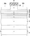
如图1所示,在包括n型GaN衬底11和在n型GaN衬底11上面生长的n型GaN层12的半导体衬底(11,12)上面制造根据本发明第一实施方案的半导体器件,n型GaN层12用例如硅(Si)原子的n型杂质原子掺杂。As shown in FIG. 1, a semiconductor according to the first embodiment of the present invention is fabricated on a semiconductor substrate (11, 12) comprising an n-
注意n型GaN层12只是一个实例。更一般地说,n型GaN层12可以是另一种III-V族氮化物化合物半导体的n型单晶层,例如InxGa1-x-yAlyN层。n型GaN衬底11具有表面取向,其由从{0001}面向<1-100>方向的表面倾角绝对值Δθ1-100和从{0001}面向<11-20>方向的表面倾角绝对值Δθ11-20来定义,这些绝对值表示如下:Note that n-
0.12度≤|Δθ1-100|≤0.35度 (1)0.12 degrees≤|Δθ1-100 |≤0.35 degrees (1)
0.00度≤|Δθ11-20|≤0.06度 (2)0.00°≤|Δθ11-20 |≤0.06° (2)
此处,<1-100>方向表示六方对称中例如[1-100]、[10-10]、[-1100]、[-1010]、[01-10]、[0-110]方向的一组等价方向,<11-20>方向表示六方对称中例如[11-20]、[1-210]、[-2110]、[-1-120]、[-12-10]、[2-1-10]方向的一组等价方向。本领域众所周知,在密勒指数中的表示中,如果平面具有负的截距,在指数上方用“线条”表示负数。我们就在主题指数前面用“-”表示,代替在指数上方使用“线条”。举例来说,<1-100>读作“one、bar one、zero、zero”。在包括n型GaN衬底11和在n型GaN衬底11上面生长的n型GaN层12的第一堆叠结构(11,12)上面形成激光二极管的器件结构部分。在第一实施方案中,第一堆叠结构(11,12)指“半导体衬底(11,12)”,其还可以被一般性地称作“外延衬底(11,12)”,并且在半导体衬底(11,12)上面通过外延连续生长器件结构部分。Here, the <1-100> direction represents one of directions such as [1-100], [10-10], [-1100], [-1010], [01-10], [0-110] in hexagonal symmetry. Group equivalent direction, <11-20> direction means hexagonal symmetry such as [11-20], [1-210], [-2110], [-1-120], [-12-10], [2- 1-10] directions for a set of equivalent directions. It is well known in the art that in representations in Miller indices, if a plane has a negative intercept, negative numbers are represented by a "line" over the exponent. Instead of using a "line" above the index, we use a "-" in front of the thematic index. For example, <1-100> is read as "one, bar one, zero, zero". A device structure portion of a laser diode is formed over a first stack structure ( 11 , 12 ) including an n-
器件结构部分通过第二堆叠结构(13,14,15,16,17,18,19,20)作为基础结构来实现,其包括n型覆盖层13、在所述n型覆盖层13上面的n型GaN光导层14、在所述n型GaN光导层14上面的活性层(发光层)15、在所述活性层(发光层)15上面的第一p型GaN光导层16、在所述第一p型GaN光导层16上面的防溢流层17、在所述防溢流层17上面的第二p型GaN光导层18、在所述第二p型GaN光导层18上面的p型覆盖层19、在所述p型覆盖层19上面的p型GaN接触层20;其中n型覆盖层13或最低层与半导体衬底(11,12)的n型GaN层12的上表面接触。注意在根据第一实施方案的半导体器件中,“器件结构部分”意指承担激光二极管主要操作的主要结构部分,其通过图1所示的第二堆叠结构(13,14,15,16,17,18,19,20)作为基础结构来实现,并且不包括第一堆叠结构(11,12)。换句话说,同已经描述的一样,只要其包括承担半导体光学器件的主要操作的主要结构,“器件结构部分”不一定意指半导体光学器件的整个器件结构。The device structure part is realized through the second stack structure (13, 14, 15, 16, 17, 18, 19, 20) as the basic structure, which includes the n-
n型覆盖层13是由未掺杂的Al0.1Ga0.9N层和用大约1×1018cm-3例如Si原子的n型杂质原子掺杂的GaN层组成的超晶格,但是不局限于所述超晶格,并且可以是由例如A10.05Ga0.95N层等组成的n型III-V族氮化物化合物半导体的单层膜(厚度大约1.5微米)。另外,使用由未掺杂的Al0.1Ga0.9N层和用大约1×1018cm-3的n型杂质原子掺杂的GaN层组成的超晶格;但是即使Al0.1Ga0.9N层和GaN层都用例如Si原子的n型杂质原子掺杂,本发明的有效性也不会改变。n型GaN光导层14是大约0.1微米厚的用大约1×1018cm-3例如Si原子的n型杂质原子掺杂的GaN层;但是更一般地说,它可以是InxGa1-x-yAlyN等的n型III-V族氮化物化合物半导体层。The n-
活性层(发光层)15通过由大约3.5纳米厚的未掺杂In0.1Ga0.9N层构成的三层量子肼(QW)层,以及由大约7纳米厚的未掺杂In0.01Ga0.99N层构成的分别交替堆叠并且夹住量子肼的阻挡层组成的多层量子肼(MQW)来实现。实现MQW的InxGa1-xN层的铟摩尔分数x只是一个实例,并且只要QW层的摩尔分数x大于阻挡层的摩尔分数x,即使使用另外的值本发明的有效性也不会改变。举例来说,In0.08Ga0.92N层可以用于QW层,并且In0.02Ga0.98N层等可以用于阻挡层。The active layer (light-emitting layer) 15 passes through a three-layer quantum hydrazine (QW) layer consisting of an approximately 3.5 nm thick undoped In0.1 Ga0.9 N layer, and an approximately 7 nm thick undoped In0.01 Ga0.99 N layer This is achieved by a multilayer quantum hydrazine (MQW) composed of barrier layers that are alternately stacked and sandwiched by quantum hydrazine. The indium mole fraction x of theInxGa1-xN layer to realize the MQW is just an example, and as long as the mole fraction x of the QW layer is greater than the mole fraction x of the barrier layer, the effectiveness of the invention does not change even if another value is used . For example, an In0.08 Ga0.92 N layer can be used for the QW layer, and an In0.02 Ga0.98 N layer or the like can be used for the barrier layer.
在活性层(发光层)15上提供的第一p型GaN光导层16应该形成的厚度约为0.03微米。The first p-type GaN
防溢流层17是防止电子溢流的层,并且由大约10纳米厚的用大约5×1018cm-3例如镁(Mg)原子的p型杂质原子掺杂的Al0.2Ga0.8N层组成。第二p型GaN光导层18是大约0.1微米厚的用大约5至10×1018cm-3例如镁(Mg)原子的p型杂质原子掺杂的GaN层组成;但是更一般地说,它可以是InxGa1-x-yAlyN等的p型III-V族氮化物化合物半导体层。The
p型覆盖层19是由未掺杂的Al0.1Ga0.9N层和用例如Mg原子的p型杂质原子掺杂的GaN层组成的超晶格,但是不局限于所述超晶格,并且可以是由例如Al0.05Ga0.95N层等组成的用大约1×1019cm-3Mg浓度掺杂的p型III-V族氮化物化合物半导体的单层膜(厚度大约0.6微米)。另外,使用由未掺杂的Al0.1Ga0.9N层和用p型杂质原子掺杂的GaN层组成的超晶格;但是即使Al0.1Ga0.9N层和GaN层都用例如Mg原子的p型杂质原子掺杂,本发明的有效性也不会改变。p型GaN接触层20是大约0.05微米厚的用大约2×1020cm-3例如Mg原子的p型杂质原子掺杂的GaN层;但是更一般地说,它可以是InxGa1-x-yAlyN等的p型III-V族氮化物化合物半导体层。The p-
注意对于外延生长图1所示的第二堆叠结构(13,14,15,16,17,18,19,20),使用金属有机化学气相沉积(MOCVD)。然后,通过使用刻蚀工艺作为器件制造工艺,在第二堆叠结构(13,14,15,16,17,18,19,20)的顶部形成2微米宽的脊结构,使得p型覆盖层19和p型GaN接触层20的堆叠结构在中央突起,实现脊结构。p型覆盖层19围绕着中央突起具有平坦的部分,从而建立了所述脊结构。换句话说,p型覆盖层19自身具有由突起和用作突起基础的平坦部分组成的反T型台阶结构。然后,在由p型覆盖层19构成的突起顶部提供p型GaN接触层20。通过包括p型覆盖层19和p型GaN接触层20的堆叠突起实现的脊结构垂直于纸平面延伸。注意所述脊结构不局限于如图1所示的具有垂直侧壁剖面的矩形脊,其可以形成在剖视图中具有台面倾斜的梯形脊。Note that for the epitaxial growth of the second stack structure (13, 14, 15, 16, 17, 18, 19, 20) shown in Figure 1, metal organic chemical vapor deposition (MOCVD) was used. Then, by using an etching process as a device manufacturing process, a 2 micron wide ridge structure is formed on the top of the second stack structure (13, 14, 15, 16, 17, 18, 19, 20), so that the p-
在p型覆盖层19上面提供绝缘膜41作为夹持脊结构(突起)的“电流阻挡层”,其围绕着突起形成一对平坦的部分,并且所述电流阻挡层以横向模式防止了激光振荡。电流阻挡层的厚度可以根据激光设计在从大约0.3微米至0.8微米的范围内任意选择,并且举例来说可以设置为大约0.5微米的值。电流阻挡层可以由例如AlN层或Al0.2Ga0.8N层、质子辐射半导体层、氧化硅膜(SiO2膜),或者氧化锆膜(ZrO2膜)的高电阻率半导体层组成。此外,该层例如还可以是由SiO2膜和ZrO2膜构成的多层膜。换句话说,各种比用于活性层(发光层)15的III-V族氮化物化合物半导体具有更低折射率的材料都可以用于电流阻挡层。对于通过p型覆盖层19和p型GaN接触层20实现的脊结构,可以使用例如n型GaN或n型AlyGa1-yN的n型半导体层作为电流阻挡层来代替使用绝缘膜41,从而建立pn结的隔离。An insulating
在p型GaN接触层20上提供例如由钯-铂-金(Pd/Pt/Au)复合膜组成的p侧电极(阳极电极)32。举例来说,Pd膜约为0.05微米厚,Pt膜约为0.05微米厚,并且Au膜约为1微米厚。在n型GaN衬底11的底表面上提供由钛-铂-金(Ti/Pt/Au)复合膜组成的n侧电极(阴极电极)31。举例来说,n侧电极(阴极电极)31可以由约0.05微米厚的Ti膜,约0.05微米厚的Pt膜和约1微米厚的Au膜来实现。通过劈开来形成激光共振腔的端面。在与发射激光的前端面相对面的后部端面上施用高反射的涂膜。A p-side electrode (anode electrode) 32 composed of, for example, a palladium-platinum-gold (Pd/Pt/Au) composite film is provided on the p-type
注意提供器件结构的n型覆盖层13、n型GaN光导层14、活性层(发光层)15、第一p型GaN光导层16、防溢流层17、第二p型GaN光导层18、p型覆盖层19和p型GaN接触层20都只是实例,并且本发明不局限于这些材料。更一般地说,根据设计选择,可以使用例如InxGa1-x-yAlyN层的另一种III-V族氮化物化合物半导体的适当单晶层。因此,上述InxGa1-xN层的铟摩尔分数x和AlyGa1-yN的铝摩尔分数y只是实例,并且甚至使用其它的摩尔分数值,当然可以实现下面的有效性。Note that the n-
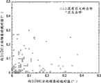
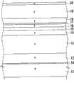
图2是表示根据本发明第一实施方案,半导体器件(激光二极管)在25℃和连续振荡条件下的电流对光输出功率特性的图,并且与相同条件下比较实施例的电流对光输出功率的特性进行了比较。图2中实线表示的电流对光输出功率特性是在GaN衬底11上结合了如图11所示的δ掺杂层10结构的结果,所述衬底具有倾角Δθ1-100和Δθ11-20满足等式(1)和等式(2)关系的表面取向。具有δ掺杂层10的激光二极管的平均阈值电流大约为45毫安。图2中点划线所示的电流对光输出功率特性是在GaN衬底11上没有结合如图11所示的δ掺杂层10结构的结果,但是GaN衬底11具有倾角Δθ1-100和Δθ11-20满足等式(1)和等式(2)关系的表面取向。不具有δ掺杂层10的激光二极管的平均阈值电流大约为55毫安。图2中虚线所示的比较实施例是通过在倾角Δθ1-100和Δθ11-20不满足等式(1)和等式(2)关系的{0001}取向的n型GaN衬底11上生长上述激光结构而制造的激光二极管。从根据比较实施例的激光二极管的电流对光输出功率特性中发现的平均阈值电流是106毫安,并且大于根据第一实施方案的半导体器件的值。比较实施例结构更高的平均阈值电流是由于发生传播光的界面平整度的波动引起的。因此,应当理解比较实施例的结构建立了比第一实施方案的结构更宽的增益分布和增加的能量损失。2 is a graph showing the current-to-light output power characteristics of a semiconductor device (laser diode) at 25° C. and continuous oscillation conditions according to the first embodiment of the present invention, and compares the current-to-light output power characteristics of Examples under the same conditions characteristics were compared. The current-to-light output power characteristic represented by the solid line in FIG. 2 is the result of combining the structure of the delta-doped
另外,通过X射线衍射的摇摆曲线比较根据第一实施方案的半导体器件(激光二极管)晶体生长后的晶片(参阅图6)。图3A和3B表示ω/2θ扫描通过(0002)面的结果。在谱图中,图3A和3B右端所示的在0arcsec(弧秒)处的峰与GaN层的衍射相应。因为n型覆盖层13是由n型Al0.1Ga0.9N层和n型GaN层组成的超晶格,并且p型覆盖层19是由p型Al0.1Ga0.9N层和p型GaN层组成的超晶格,所以除了在0级衍射处的峰外,还可以检测到例如相应于超晶格周期的在负第一级和正第一级衍射处的两个伴峰。即,在图3A和3B中接近-3200弧秒处观察到的伴峰是归属于Al0.1Ga0.9N/GaN超晶格的负第一级伴峰。In addition, the wafer after crystal growth of the semiconductor device (laser diode) according to the first embodiment was compared by the rocking curve of X-ray diffraction (see FIG. 6 ). Figures 3A and 3B show the results of ω/2Θ scans through the (0002) plane. In the spectrograms, the peak at 0 arcsec (arc second) shown on the right end of FIGS. 3A and 3B corresponds to the diffraction of the GaN layer. Because the n-
如图3A所示,具有在GaN衬底11上面生长的上述激光结构的晶片伴峰的半峰全宽(FWHM)为145弧秒,所述衬底具有倾角Δθ1-100和Δθ11-20满足等式(1)和等式(2)关系的表面取向。另一方面,如图3B所示,具有在倾角Δθ1-100和Δθ11-20不满足等式(1)和等式(2)关系的{0001}取向GaN衬底11上面生长的上述激光结构的晶片伴峰的FWHM为367弧秒,该值是宽的。宽的FWHM意指观察覆盖层的整个表面时,超晶格界面的陡峭度和膜表面的平整度不好。As shown in FIG. 3A, the full width at half maximum (FWHM) of the wafer satellite having the above-mentioned laser structure grown on a
通过诺马尔斯基显微镜观察生长的晶片的结果在图4中给出。图4中,沿着横坐标绘制从{0001}面向[1-100]方向的表面倾角Δθ1-100绝对值,并且沿着纵坐标绘制从{0001}面向[11-20]方向的表面倾角Δθ11-20绝对值。图4中,在位于0.12度和0.35度之间的各个倾角Δθ1-100的绝对值范围内,以及位于0.00度和0.06度之间的各个倾角Δθ11-20的绝对值范围内,观察到没有巨大台阶的有利的平整度,由空心圆圈(○)、空心三角(△)和空心方框(□)表示。因为X射线摇摆曲线的FWHM位于200至250弧秒的范围内,并且可以获得平整的表面,所以更优选各个倾角Δθ1-100的绝对值在0.12度至0.35度的范围内,并且各个倾角Δθ11-20的绝对值在0.00度至0.06度的范围内,由空心三角符号和空心圆圈符号表示。因为X射线摇摆曲线的FWHM变成约150弧秒,并且可以获得镜面般的表面而不存在巨大的台阶,所以甚至更优选各个倾角Δθ1-100的绝对值在0.14度至0.28度的范围内,并且各个倾角Δθ11-20的绝对值在0.00度至0.06度的范围内,由空心圆圈符号表示。换句话说,当在GaN衬底11上生长了如图1所示激光结构的上述晶片的表面形貌了实现了器件尺寸所需的非常平滑的镜面时,所述GaN衬底11具有倾角Δθ1-100和Δθ11-20满足等式(1)和等式(2)关系的晶面取向,在倾角Δθ1-100和Δθ11-20不满足等式(1)和等式(2)关系的{0001}取向的GaN衬底11上面生长了上述激光结构的晶片的表面形貌产生在几十至几百微米量级的巨大台阶,从而形成不平的表面。The results of observation of the grown wafer by a Nomarski microscope are given in FIG. 4 . In Figure 4, the absolute value of the surface inclination angle Δθ1-100 from {0001} facing the [1-100] direction is plotted along the abscissa, and the surface inclination angle from {0001} facing the [11-20] direction is plotted along the ordinate Δθ11-20 absolute value. In Fig. 4, in the absolute value range of the respective inclination angles Δθ1-100 lying between 0.12 degrees and 0.35 degrees, and in the absolute value range of the respective inclination angles Δθ11-20 lying between 0.00 degrees and 0.06 degrees, it is observed that Favorable flatness without huge steps, indicated by open circles (○), open triangles (Δ) and open squares (□). Because the FWHM of the X-ray rocking curve is in the range of 200 to 250 arc seconds, and a flat surface can be obtained, it is more preferable that the absolute value of each inclination angle Δθ1-100 is in the range of 0.12 degrees to 0.35 degrees, and each inclination angle Δθ The absolute value of11-20 is in the range of 0.00 degrees to 0.06 degrees, represented by the open triangle symbol and the open circle symbol. Since the FWHM of the X-ray rocking curve becomes about 150 arc seconds and a mirror-like surface can be obtained without huge steps, it is even more preferable that the absolute values of the respective inclination angles Δθ1-100 be in the range of 0.14 degrees to 0.28 degrees , and the absolute value of each inclination angle Δθ11-20 is in the range of 0.00 degrees to 0.06 degrees, represented by a hollow circle symbol. In other words, when the surface topography of the above-mentioned wafer on which the laser structure shown in FIG.1-100 and Δθ11-20 satisfy the crystal plane orientation of the relationship of equation (1) and equation (2), and the inclination angle Δθ1-100 and Δθ11-20 do not satisfy equation (1) and equation (2) The surface topography of the {0001}-oriented
因而,因为根据第一实施方案的半导体衬底(外延衬底)生长在GaN衬底11上面,所以基本上很少有例如引线错位和外延生长层裂纹的缺陷问题,所述缺陷归因于晶格与衬底失配。另外,因为优化了GaN衬底11的晶面取向,所以获得具有有利的表面形貌和表面平整度的III-V族氮化物化合物半导体外延生长层。此外,使用具有优异表面平整度的半导体衬底(外延衬底)的根据第一实施方案的半导体器件(激光二极管)便于制造具有很少光学损失,并且提供降低的阈值电流、增加的操作寿命和改善的可靠性的波导。另外,根据与第一实施方案相关的半导体器件(激光二极管),阻止了增益分布的空间膨胀,从而提供了高效率的器件。Thus, since the semiconductor substrate (epitaxial substrate) according to the first embodiment is grown over the
[器件制造][Device Manufacturing]
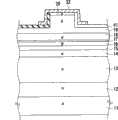
参照图5至11说明根据本发明第一实施方案的半导体器件(激光二极管)的制造方法。注意所述半导体器件的制造方法只是一个实例,并且本发明可以自然地通过使用包括各种改进的各种制造方法来实现。举例来说,根据第一实施方案的半导体器件(激光二极管)制造方法中使用的晶体生长炉以MOCVD炉来说明,但是其可以通过使用例如分子束外延(MBE)炉的其它晶体生长炉的其它方法来制造。A method of manufacturing a semiconductor device (laser diode) according to a first embodiment of the present invention will be described with reference to FIGS. 5 to 11 . Note that the manufacturing method of the semiconductor device is just an example, and the present invention can naturally be realized by using various manufacturing methods including various improvements. For example, the crystal growth furnace used in the manufacturing method of the semiconductor device (laser diode) according to the first embodiment is explained as an MOCVD furnace, but it can be changed by using other crystal growth furnaces such as molecular beam epitaxy (MBE) furnaces. method to manufacture.
(a)首先,如图5A所示,制造具有倾角Δθ1-100和Δθ11-20满足等式(1)和等式(2)关系的表面取向的GaN衬底11。然后,将GaN衬底11固定到MOCVD炉的接受器上。在包括作为V族元素原料气的氨气(NH3)的气氛中开始热处理。与氢气(H2)一块鼓泡作为III族元素原料气的例如三甲基镓(Ga(CH3)3)气体或三乙基镓(Ga(C2H5)3)气体的金属有机镓化合物气体,然后引入生长室,其中GaN衬底11被加热到1000至1100℃的衬底温度下。如图5B所示,在GaN衬底11上面生长n型GaN层12,提供半导体衬底(11,12)。当在GaN衬底11上生长n型GaN层12时,优选几百或更大的高V/III比。可以使用例如硅烷(SiH4)气体的Si氢化物或者例如四甲基硅烷(Si(CH3)4)气体的有机硅化合物气体作为n型掺杂材料。(a) First, as shown in FIG. 5A ,
(b)接着,一旦衬底温度达到1000℃至1080℃之间,对于激光二极管的器件结构部分,在半导体衬底(11,12)的n型GaN层12上面实施连续外延生长。换句话说,如图5C所示,在同一个生长室(反应管)中,通过连续外延生长在n型GaN层12上面生长n型覆盖层13。此外,如图6所示,在n型覆盖层13之后,以连续的顺序外延生长n型GaN光导层14、活性层(发光层)15、第一p型GaN光导层16、防溢流层17、第二p型GaN光导层18、p型覆盖层19和p型GaN接触层20,从而形成双异质结结构。作为III族材料,可以使用例如三甲基镓(Ga(CH3)3)气体或三乙基镓(Ga(C2H5)3)气体的金属有机镓化合物、例如三甲基铝(Al(CH3)3)气体或三乙基铝(Al(C2H5)3)气体的金属有机铝化合物,以及例如三甲基铟(In(CH3)3)气体或三乙基铟(In(C2H5)3)气体的金属有机铟化合物。当生长外延层14、15、16、17、18、19和20时,分别优选几百或更大的高V/III比。n型覆盖层13是约1.5微米厚的具有约1×1018cm-3Si浓度的外延层,并且n型GaN光导层14是约0.1微米厚的具有约1×1018cm-3Si浓度的外延层。在所述n型GaN光导层14上提供的活性层(发光层)15具有通过交替堆叠由三层In0.1Ga0.9N层组成的量子肼(QW)层和由五层In0.01Ga0.99N层组成的阻挡层形成的三层周期MQW结构。在所述活性层(发光层)15上提供的第一p型GaN光导层16是约0.03微米厚的外延层;所述防溢流层17是约10纳米厚的具有约5×1018cm-3Mg浓度的外延层;所述第二p型GaN光导层18是约0.1微米厚的具有约5至10×1018cm-3Mg浓度的外延层;所述p型覆盖层19是约0.6微米厚的具有约1×1019cm-3Mg浓度的外延层;并且所述p型GaN接触层20是约0.05微米厚的具有约2×1020cm-3Mg浓度的外延层。例如双环茂二烯镁(Cp2Mg原子)或双甲基-环茂二烯镁(M2Cp2Mg原子)的金属有机镁化合物可以用作p型掺杂材料。(b) Next, once the substrate temperature reaches between 1000°C and 1080°C, continuous epitaxial growth is performed on the n-
(c)接下来,如图7所示,使用光刻胶51作为掩模,通过使p型覆盖层19和p型GaN接触层20接受反应离子刻蚀(RIE),选择性地形成沟槽50a和50b,留下由沟槽50a和50b围绕的突起。由p型覆盖层19和p型GaN接触层20形成的梯形突起形成脊结构,垂直于纸的平面延伸。在p型覆盖层19和p型GaN接触层20的厚度分别约为0.6微米和约0.05微米的情况中,每个沟槽50a和50b的厚度应该约为0.5微米。(c) Next, as shown in FIG. 7, trenches are selectively formed by subjecting the p-
(d)接下来,如图8所示,一旦除去光刻胶,填充沟槽50a和50b,然后在整个表面上沉积约0.6至1微米厚的绝缘膜41,从而夹持由p型覆盖层19和p型GaN接触层20形成的脊(突起)。对于绝缘膜41,可以外延生长例如AlN层的高电阻率半导体层,或者通过CVD沉积氧化硅膜(SiO2膜)。如图9所示,然后仅刻蚀p型GaN接触层20上面的绝缘膜41,直至暴露出p型GaN接触层20的上表面。(d) Next, as shown in FIG. 8, once the photoresist is removed, the
(e)接下来,如图10所示,使用溶脱方法在p型GaN接触层20上面描绘出由钯-铂-金(Pd/Pt/Au)复合膜组成的p侧电极(阳极电极)32。换句话说,在p型GaN接触层20两侧上的p型GaN接触层20和绝缘膜41上面形成具有相应于p侧电极(阳极电极)32图案的窗口的光刻胶膜后,通过真空蒸镀或溅射连续沉积约0.05微米厚的Pd膜、约0.05微米厚的Pt膜和约1微米厚的Au膜,然后剥离光刻胶膜,在所述窗口位置留下p侧电极(阳极电极)32。此外,通过CVD沉积例如氧化硅膜(SiO2膜)、氮化硅膜(Si3N4膜)或聚酰亚胺膜的钝化膜42,从而覆盖p侧电极(阳极电极)32和绝缘膜41。然后,使用如图1所示的背部刻蚀方法,选择性除去部分钝化膜42,使得p侧电极(阳极电极)32的上表面可见。随后,通过真空蒸镀或溅射在GaN衬底11的下表面上沉积钛-铂-金(Ti/Pt/Au)复合膜。举例来说,连续沉积约0.05微米厚的Ti层,约0.05微米厚的Pt层和约1.0微米厚的Au膜。然后,通过热处理(烧结),降低p侧电极(阳极电极)32和n侧电极(阴极电极)31的接触电阻。通过分裂或使用例如金刚石刀片的切割装置提供所需的大小,完成图1所示的半导体器件(激光二极管)。(e) Next, as shown in FIG. 10, a p-side electrode (anode electrode) 32 composed of a palladium-platinum-gold (Pd/Pt/Au) composite film is drawn on the p-type
如上所述,因为根据本发明第一实施方案的半导体器件制造方法,外延层生长在GaN衬底11上面,所以基本上很少有例如引线错位和裂纹的缺陷问题,所述缺陷与外延生长层和GaN衬底11之间的晶格失配有关。另外,因为优化了GaN衬底11的晶面取向,表面形貌和表面平整度是有利的。因此,在n侧GaN衬底11上面均匀地生长出高晶体学质量的III-V族氮化物化合物半导体外延层。因此,提供了具有优异的产率和低成本的高性能III-V族氮化物化合物半导体。As described above, since the epitaxial layer is grown on the
[第一实施方案的改进][Improvement of the first embodiment]
如图11所示,根据本发明第一实施方案改进的半导体器件(激光二极管)与根据本发明第一实施方案的半导体器件不同,其中n型GaN层12的堆叠结构(11,10,12)进一步包括δ掺杂层(delta掺杂层)10。δ掺杂层10生长在具有倾角Δθ1-100和Δθ11-20满足等式(1)和等式(2)关系的表面取向的GaN衬底11上面。另外,n型GaN层12通过δ掺杂层10生长在GaN衬底11上面。其它结构和材料,例如通过依次具有n型覆盖层13、n型GaN光导层14、活性层(发光层)15、第一p型GaN光导层16、防溢流层17、第二p型GaN光导层18、p型覆盖层19和p型GaN接触层20的堆叠结构实现的激光二极管的器件结构部分,所述堆叠结构在n型GaN层12上形成,脊结构的结构、电极等都与参照图1已经在第一实施方案中解释的结构和材料相似,并且在第一实施方案的改进中省略了交叠或多余的说明。As shown in FIG. 11, the semiconductor device (laser diode) improved according to the first embodiment of the present invention is different from the semiconductor device according to the first embodiment of the present invention, wherein the stacked structure of the n-type GaN layer 12 (11, 10, 12) It further includes a delta-doped layer (delta-doped layer) 10 . The delta-doped
δ掺杂层10是用例如Si原子的n型杂质原子掺杂的厚度为大约200纳米或更小的GaN层,杂质浓度至少约5×1017cm-3并且不大于2×1019cm-3,优选至少约1×1018cm-3并且不大于2×1019cm-3,甚至更优选至少约4×1018cm-3并且不大于2×1019cm-3。δ掺杂层10的厚度下限等于原子层厚度或者大约0.3纳米。δ掺杂层10的厚度应该优选落在原子层厚度至约150纳米的范围内,更优选在约5纳米和约150纳米之间。当δ掺杂层10的杂质浓度超过约2×1019cm-3时,生长在δ掺杂层10上面的n型GaN层12的上表面变得粗糙。The delta-doped
换句话说,当形成用至少约4×1018cm-3并且不大于2×1019cm-3的例如Si原子的n型杂质原子掺杂的δ掺杂层10,作为优选的形式使其厚度在原子层厚度至约200纳米的范围内时,可以加速向衬底表面内的外侧晶体生长速度,改善外延生长层上表面的平整度。但是,外侧晶体生长作用在杂质浓度降低至小于等于约4×1018cm-3时是不显著的。随着杂质降低至小于等于约1×1018cm-3,有效性进一步降低,并且当杂质浓度降低至小于等于约5×1017cm-3时,更难实现外侧晶体生长速度的加速和表面平整度的改善。In other words, when the δ-doped
因此,根据与第一实施方案改进相关的半导体器件(激光二极管),在n型GaN层12和n型GaN衬底11之间提供δ掺杂层10,从而加速沿着n型GaN衬底11表面向内的外侧晶体生长速度。与图1所示根据第一实施方案不具有δ掺杂层10的半导体器件相比,外侧晶体生长的加速便于改善所生长晶片表面形貌的平整度。结果,如图2所示,根据第一实施方案改进的半导体器件(激光二极管)的平均阈值电流降低至45毫安,操作寿命延长,并且可靠性进一步提高。Therefore, according to the semiconductor device (laser diode) related to the modification of the first embodiment, the delta-doped
通过根据第一实施方案改进的半导体器件(激光二极管)制造方法,如图12所示,当借助δ掺杂层10,在具有倾角Δθ1-100和Δθ11-20满足等式(1)和等式(2)关系的表面取向的GaN衬底11上沉积n型GaN层12,并且然后连续外延生长n型覆盖层13、n型GaN光导层14、活性层(发光层)15、第一p型GaN光导层16、防溢流层17、第二p型GaN光导层18、p型覆盖层19和p型GaN接触层20时,后续步骤基本上与图7至图10中所示的程序相同,并且省略了其重复的说明。By the improved semiconductor device (laser diode) manufacturing methodaccording to the first embodiment, as shownin FIG. Deposit n-
(第二实施方案)(second embodiment)
如图13所示,根据本发明第二实施方案的半导体器件与已经在第一实施方案中解释了的半导体器件相同,其中半导体器件在第一堆叠结构(11,12)上面形成,所述堆叠结构通过例如在倾角Δθ1-100和Δθ11-20满足等式(1)和等式(2)关系的GaN衬底11上面生长n型GaN层12的方法来实现。As shown in FIG. 13, the semiconductor device according to the second embodiment of the present invention is the same as the semiconductor device explained in the first embodiment, wherein the semiconductor device is formed above the first stack structure (11, 12), the stack The structure is realized by, for example, a method of growing n-
但是,在根据第二实施方案的半导体器件中,实现发光二极管(LED)的器件结构部分在第一堆叠结构(11,12)上面形成。如同第一实施方案所述,n型GaN层12只是一个实例。更一般地说,n型GaN层12可以是另一种III-V族氮化物化合物半导体的n型单晶层,例如InxGa1-x-yAlyN层。However, in the semiconductor device according to the second embodiment, part of the device structure realizing a light emitting diode (LED) is formed over the first stacked structure (11, 12). As described in the first embodiment, the n-
换句话说,如图13所示,直接在n型GaN层12或者第一堆叠结构(11,12)的上层上面外延生长由Si掺杂的Al0.05Ga0.95N层构成的n型覆盖层13,并且依次在n型覆盖层13上面连续堆叠由InxGa1-xN层构成活性层(发光层)21、由Mg掺杂的Al0.05Ga0.95N层构成的p型覆盖层19,以及由Mg掺杂的GaN层构成的p型GaN接触层20。此外,在p型GaN接触层20上面形成实现p侧电极(阳极电极)33的透明电极。In other words, as shown in FIG. 13 , the n-
发光二极管(LED)的器件结构的细节,例如n型覆盖层13、InxGa1-xN活性层21、p型覆盖层19和p型GaN接触层20基本上与已经在第一实施方案中解释了的半导体器件相同,并且省略了其重复的说明。此外,在根据第二实施方案的半导体器件中,“器件结构部分”意指承担LED主要操作的主要结构,其通过图13中所示的第二堆叠结构(13,21,19,20)作为基础结构来实现,并且不包括在器件结构部分下方用作n型接触层的第一堆叠结构(11,12)。换句话说,只要其包括承担半导体光学器件的主要操作的主要结构部分,“器件结构部分”不一定意指光学半导体器件的整个器件结构,这与已经在第一实施方案中解释了的半导体器件的意义相同。Details of the device structure of a light emitting diode (LED), such as the n-
如同第一实施方案所述,形成器件结构部分的n型覆盖层13、InxGa1-xN活性层21、p型覆盖层19和p型GaN接触层20只是一个实例,并且本发明不局限于这些材料。换句话说,更一般地说,对于形成器件结构部分的每一层都可以使用其它III-V族氮化物化合物半导体的单晶层,例如InxGa1-x-yAlyN层。As described in the first embodiment, the n-
因为根据第二实施方案的半导体衬底(外延衬底)具有GaN衬底11,所以基本上很少有例如引线错位和裂纹的缺陷问题,所述缺陷可以归因于外延生长层与GaN衬底11之间的晶格失配。另外,因为优化了GaN衬底11的晶面取向,所以可以获得具有有利的表面形貌和表面平整度的III-V族氮化物化合物半导体外延生长层。此外,根据第二实施方案的半导体器件(LED)使用具有优异表面平整度的半导体衬底,因此可以实现特性的改善,例如使用低的操作电压、高亮度、高发光效率等。Since the semiconductor substrate (epitaxial substrate) according to the second embodiment has the
尽管从图片中省略了,但是甚至在图11所示的根据本发明第二实施方案的半导体器件(LED)的情况下,优选借助δ掺杂层10,在n型GaN衬底11上面生长n型GaN层12。如同第一实施方案所述,δ掺杂层10是用n型杂质原子掺杂的厚度小于约200纳米的GaN层,杂质浓度至少约5×1017cm-3并且不大于2×1019cm-3,优选至少约1×1018cm-3并且不大于2×1019cm-3,甚至更优选至少约4×1018cm-3并且不大于2×1019cm-3。δ掺杂层10的厚度应该优选落在原子层厚度至约150纳米的范围内,更优选在约5纳米和约150纳米之间。当δ掺杂层10的杂质浓度超过约2×1019cm-3时,生长其上面的n型GaN层12的上表面变得粗糙,并因此是不可取的。当形成用至少约4×1018cm-3并且不大于2×1019cm-3的n型杂质原子掺杂的层,使其厚度在原子层厚度至约200纳米的范围内时,可以加速向衬底表面内的外侧晶体生长速度,改善外延生长层上表面的平整度。当杂质浓度降低至小于等于约4×1018cm-3时,外侧晶体生长速度的加速作用是不显著的。当杂质降低至小于等于约1×1018cm-3,外侧晶体生长速度的加速作用进一步降低;并且当杂质浓度降低至小于等于约5×1017cm-3时,几乎不能实现外侧晶体生长速度的加速作用和表面平整度的改善。在n型GaN层12和n型GaN衬底11之间插入δ掺杂层10便于进一步改善表面形貌和表面平整度,提供了根据第二实施方案的半导体器件(LED)进一步的特性改善,例如在低的操作电压下操作、高亮度、高发光效率等。Although omitted from the picture, even in the case of the semiconductor device (LED) according to the second embodiment of the present invention shown in FIG.
[器件制造][Device Manufacturing]
根据本发明第二实施方案的半导体器件的制造方法基本上与已经在图5A-5C、6、7、8、9、10中所示第一实施方案中解释了的半导体器件的制造方法相同。The manufacturing method of the semiconductor device according to the second embodiment of the present invention is basically the same as that already explained in the first embodiment shown in FIGS. 5A-5C , 6 , 7 , 8 , 9 , 10 .
(a)首先,如图14所示,直接在n型GaN层12或第一堆叠结构(11,12)的上层上面外延生长由Si掺杂的Al0.05Ga0.95N层构成的n型覆盖层13,所述第一堆叠结构(11,12)用作半导体衬底或者外延衬底。然后,依次在n型覆盖层13上面连续外延生长InxGa1-xN活性层(发光层)21、p型覆盖层19和p型GaN接触层20。(a) First, as shown in FIG. 14 , epitaxially grow an n-type cladding layer composed of a Si-doped Al0.05 Ga0.95 N layer directly on the n-
(b)此外,在p型GaN接触层20上面形成由例如锡(Sn)掺杂的氧化铟(In2O3)膜(ITO)、铟(In)掺杂的氧化锌(ZnO)膜(IZO)、镓(Ga)掺杂的氧化锌膜(GZO)、氧化锡(SnO2)膜等的透明电极组成的p侧电极(阳极电极)33。可选地,透明电极可以是沉积得很薄,从而保持光学透明度的金(Au)、镍(Ni)等的金属薄膜。(b) Further, on the p-type
(c)随后,如图13所示,通过真空蒸镀或溅射在n型GaN衬底11的下表面上沉积钛-铂-金(Ti/Pt/Au)复合膜。举例来说,连续沉积约0.05微米厚的Ti膜,约0.05微米厚的Pt膜和约1微米厚的Au膜。然后,实施热处理(烧结),从而接触n侧电极(阴极电极)31的接触电阻。通过劈开,或者通过使用例如金刚石刀片的切割装置提供所需的尺寸,完成如图13所示的半导体器件(发光二极管(LED))。(c) Subsequently, as shown in FIG. 13 , a titanium-platinum-gold (Ti/Pt/Au) composite film is deposited on the lower surface of n-
如上所述,因为根据本发明第二实施方案的半导体器件制造方法使用GaN衬底11,所以基本上很少有例如引线错位和裂纹的缺陷问题,所述缺陷归因于外延生长层和GaN衬底11之间的晶格失配。另外,因为优化了GaN衬底11的晶面取向,所以表面形貌和表面平整度是有利的。因此,在n型GaN衬底11上面均匀地生长出高晶体学质量的III-V族氮化物化合物半导体外延层。因此,提供了具有优异的产率和低成本的高性能III-V族氮化物化合物半导体器件。As described above, since the semiconductor device manufacturing method according to the second embodiment of the present invention uses the
(第三实施方案)(third embodiment)
如图15所示,根据本发明第三实施方案的半导体器件通过器件结构部分(26,25,24)实现了异质结双极晶体管(HBT),所述器件结构部分(26,25,24)通过在倾角Δθ1-100和Δθ11-20满足等式(1)和等式(2)关系的GaN衬底11上面连续堆叠由Si掺杂的GaN层构成的n型漂移层24、由Mg掺杂的InxGa1-xN层构成的p型基础层25和由Si掺杂层构成的n型发射层26来形成。n型GaN衬底11用作集电极层(集电极接触层)。As shown in FIG. 15, the semiconductor device according to the third embodiment of the present invention realizes a heterojunction bipolar transistor (HBT) through the device structure part (26, 25, 24), and the device structure part (26, 25, 24 ) by continuously stacking an n-
n型漂移层(drift layer)24是约0.3至1.5微米厚并且用浓度约1×10¹⁴至5×1016cm-3的Si原子掺杂的III-V族氮化物化合物半导体的单晶层。当p型基础层25的Mg浓度和厚度可以考虑HBT的操作频率和击穿电压来确定时,Mg浓度应当选择落在约5×10¹⁸至7×1019cm-3之间,并且厚度落在约5至80纳米之间。n型发射层26是约0.2至0.5微米厚并且用浓度约3×10¹⁸至6×1018cm-3的Si原子掺杂的III-V族氮化物化合物半导体的单晶层。如图15所示,在n型发射层26上面提供了由钛-铂-金(Ti/Pt/Au)复合膜构成的发射极45。举例来说,发射极45可以由约0.04微米厚的Ti膜,约0.04微米厚的Pt膜和约0.5微米厚的Au膜组成。此外,形成基极底槽,穿过n型发射层26并且暴露出p型基础层25的一部分上表面。基极44与p型基础层25在基极底槽的底部产生欧姆接触。举例来说,基极44由钯-铂-金(Pd/Pt/Au)复合膜构成,其中可以使用约0.05微米厚的Pd膜,约0.05微米厚的Pt膜和约0.2微米厚的Au膜。The n-type drift layer (drift layer) 24 is a single crystal layer of group III-V nitride compound semiconductor about 0.3 to 1.5 microns thick and doped with Si atoms at a concentration of about 1×10¹⁴ to 5×1016 cm−3 . When the Mg concentration and thickness of the p-
在n型GaN衬底11的下表面上沉积由钛-铂-金(Ti/Pt/Au)复合膜构成的集电极43。与发射极45一样,集电极43可以由约0.04微米厚的Ti膜,约0.04微米厚的Pt膜和约0.5微米厚的Au膜的组合来组成。On the lower surface of n-
因此,因为根据第三实施方案的半导体衬底(外延衬底)具有GaN衬底11,所以基本上很少有与外延生长层与GaN衬底11晶格失配相关的例如引线错位和裂纹的缺陷问题。另外,因为优化了GaN衬底11的晶面取向,所以可以提供具有有利的表面形貌和表面平整度的III-V族氮化物化合物半导体的外延生长层。Therefore, since the semiconductor substrate (epitaxial substrate) according to the third embodiment has the
此外,因为根据第三实施方案的半导体器件(HBT)通过具有优异表面平整度的半导体衬底(外延衬底)来实现,所以电流增益β增加,高频特性改善,并且电流截止频率fT提高。Furthermore, since the semiconductor device (HBT) according to the third embodiment is realized by a semiconductor substrate (epitaxial substrate) having excellent surface flatness, the current gain β increases, the high-frequency characteristics improve, and the current cut-off frequency fT increases .
注意如同第一和第二实施方案所述,n型漂移层24、p型基础层25和n型发射层26的各自的材料只是实例。更一般地说,可以选择其它III-V族氮化物化合物半导体的n型单晶层,例如InxGa1-x-yAlyN层,从而满足HBT所需的禁止带隙关系。换句话说,如果选择n型发射层26的带隙,满足比p型基础层25的带隙更宽的“宽带隙发射器”,对于各层24、25和26可以选择各种III-V族氮化物化合物半导体的单晶层。举例来说,可以在n型GaN衬底11上面提供由GaN层构成的n型漂移层24、由GaN层构成的p型基础层25和由AlyGa1-yN层构成的n型发射层26。Note that as described in the first and second embodiments, the respective materials of the n-
注意在根据本发明的第三实施方案的半导体器件中,“器件结构部分”意指n型漂移层24、p型基础层25和n型发射层26,并且不包括用作集电极层(集电极接触层)的n型GaN衬底11。换句话说,只要其包括承担半导体电子器件的主要操作的主要结构部分,根据第三实施方案的半导体器件的“器件结构部分”不一定意指半导体器件的整个器件结构,这与根据第一和第二实施方案的半导体器件所述是相同的。Note that in the semiconductor device according to the third embodiment of the present invention, "device structure part" means n-
尽管从图片中省略了,但是甚至在图11所示的根据本发明第三实施方案的半导体器件(HBT)的情况下,优选借助δ掺杂层10,在n型GaN衬底11上面生长n型漂移层24。如同第一实施方案所述,δ掺杂层10是用n型杂质原子掺杂的厚度小于约200纳米的GaN层,杂质浓度至少约5×1017cm-3并且不大于2×1019cm-3,优选至少约1×1018cm-3并且不大于2×1019cm-3,甚至更优选至少约4×1018cm-3并且不大于2×1019cm-3。δ掺杂层10的厚度应该优选落在原子层厚度至约150纳米的范围内,更优选在约5纳米和约150纳米之间。使用δ掺杂层10允许更有利的表面形貌和表面平整度,并因此根据第三实施方案的半导体器件(HBT)的电流增益β进一步增加,并且还进一步改善了高频特性。Although omitted from the drawing, even in the case of the semiconductor device (HBT) according to the third embodiment of the present invention shown in FIG.
[器件制造][Device Manufacturing]
根据本发明第三实施方案的半导体器件的制造方法基本上与根据第一和第二实施方案的半导体器件的制造方法相同。The manufacturing method of the semiconductor device according to the third embodiment of the present invention is basically the same as the manufacturing methods of the semiconductor devices according to the first and second embodiments.
(a)首先,将n型GaN衬底11插入MOCVD炉中,并且如同根据第二实施方案的半导体器件的制造方法所述,如图16所示,在n型GaN衬底11依次连续外延生长由Si掺杂的GaN层构成的n型漂移层24、由Mg掺杂的In0.1Ga0.9N层构成的p型基础层25和由Si掺杂GaN层构成的n型发射层26。在n型GaN衬底11上面生长的包括n型GaN衬底11和n型漂移层24的堆叠结构(11,24)可以相应于第一和第二实施方案的半导体衬底(11,12)。但是,由n型GaN衬底11、n型漂移层24、p型基础层25和n型发射层26构成的整个堆叠结构(11,24,25,26)可以被称作“半导体衬底(外延衬底)”。连续的外延生长基本上与参考图14所述的根据第二实施方案的半导体器件制造方法相同,并且省略了其重复的说明。(a) First, an n-
(b)随后,通过光刻在n型发射层26的上表面上描绘用于基极底槽形成的光刻胶膜图案,并且使用光刻胶膜图案作为刻蚀掩模,通过例如RIE的刻蚀形成基极底槽,其穿过n型发射层26并且暴露出p型基础层25的一部分上表面。(b) Subsequently, a photoresist film pattern for base bottom groove formation is drawn on the upper surface of the n-
(c)在n型发射层26上面沉积由钛-铂-金(Ti/Pt/Au)复合膜构成的发射极45,并且在n型GaN衬底11的下表面上面描绘由钛-铂-金(Ti/Pt/Au)复合膜构成的集电极43的图案。然后,热处理(烧结)后,发射极45和集电极43的接触电极降低了。(c) Deposit an
(d)此外,如图15所示,使用溶脱方法在p型基础层25上面描绘出由Pd/Pt/Au复合膜构成的基极44。换句话说,在具有相应于p侧电极(阳极电极)44图案的窗口的光刻胶膜形成后,通过真空蒸镀或溅射连续沉积约0.04微米厚的Ti膜,约0.04微米厚的Pt膜和约0.5微米厚的Au膜,然后剥离光刻胶膜,从而在窗口位置留下基极44的图案。(d) Furthermore, as shown in FIG. 15, a
如上所述,因为根据本发明第三实施方案的半导体器件制造方法使用GaN衬底11,所以基本上很少有与外延生长层和GaN衬底11之间的晶格失配相关的例如引线错位和裂纹的缺陷问题。另外,因为优化了GaN衬底11的晶面取向,所以表面形貌和表面平整度是有利的。因此,在n型GaN衬底11上面均匀地生长出高晶体学质量的III-V族氮化物化合物半导体外延层。因此,提供了具有优异的产率和低成本的高性能III-V族氮化物化合物半导体器件。As described above, since the semiconductor device manufacturing method according to the third embodiment of the present invention uses the
(其它实施方案)(other implementations)
在接收本发明的教导后,本领域技术人员可以做出各种修改而不会背离本发明的范围。举例来说,本发明不局限于第一、第二和第三实施方案所述的激光二极管、LED或HBT,并且可选地可以应用于各种半导体器件,包括各种半导体电子器件,例如高电子迁移率晶体管(HEMT)、结场效应晶体管(FET)、肖特基栅极FET(MESFET),或者静电感应晶体管(SIT),或者例如半导体光检测器的半导体光学器件。After receiving the teachings of the present invention, various modifications can be made by those skilled in the art without departing from the scope of the present invention. For example, the present invention is not limited to laser diodes, LEDs, or HBTs described in the first, second, and third embodiments, and can optionally be applied to various semiconductor devices including various semiconductor electronic devices such as high An Electron Mobility Transistor (HEMT), a Junction Field Effect Transistor (FET), a Schottky Gate FET (MESFET), or a Static Induction Transistor (SIT), or a semiconductor optical device such as a semiconductor photodetector.
作为所述半导体电子器件的一个实例,图17表示通过器件结构部分(62,63,64,65,66)实现的HEMT的示意结构。器件结构部分(62,63,64,65,66)通过在GaN衬底61上面连续堆叠非有意掺杂的GaN层(第一单晶层)62和非有意掺杂的AlxGa1-xN层(第二单晶层)63,所述GaN衬底61是倾角Δθ1-100和Δθ11-20满足等式(1)和等式(2)关系的高电阻率的衬底,或者半绝缘衬底。非有意掺杂的GaN层62是厚度约为0.8至4.5微米并且没有故意用杂质原子掺杂的单晶层。非有意掺杂的AlxGa1-xN层63是厚度约为60至150纳米并且没有故意用杂质原子掺杂的单晶层。由于掺杂GaN层62的更大的电子亲和力,在非有意掺杂的GaN层62的上表面和其中形成两维的电子气64。形成n型源极区65和n型漏极区66,穿过非有意掺杂的AlxGa1-xN层63,进入非有意掺杂的GaN层62中。源极区65和漏极区66用例如Si原子的n型杂质原子重掺杂,掺杂浓度举例来说至少约1×1017cm-3并且不大于约1×1019cm-3。如图17所示,分别在n型源极区65和n型漏极区66的上面形成由钛-铝(Ti/AL)复合膜构成的源极71和漏极72。形成由铂-金(Pt/Au)复合膜构成的T型栅电极73,从而在n型源极区65和n型漏极区66之间的非有意掺杂的AlxGa1-xN层63上面实现肖特基耗尽栅极。非有意掺杂的AlxGa1-xN层63在异质结界面附近流动电荷完全耗尽,并且起着好像MOSEFET的栅氧化物的作用。通过Pt/Au肖特基耗尽栅极73的存在,在Pt/Au肖特基耗尽栅极73的下方形成耗尽层。向肖特基耗尽栅极73施用负偏压将使扩展栅耗尽区向异质结界面延伸,从而升高电子流动的势垒,因而节流漏-源电流(主电流)。As an example of the semiconductor electronic device, FIG. 17 shows a schematic structure of a HEMT realized by device structure sections (62, 63, 64, 65, 66). The device structure part (62, 63, 64, 65, 66) continuously stacks an unintentionally doped GaN layer (first single crystal layer) 62 and an unintentionally dopedAlxGa1-x layer on a GaN substrate 61 N layer (second single crystal layer) 63, the
使用这种结构,因为根据其它实施方案的半导体衬底(63,62,61)具有GaN衬底61,所以基本上很少有与外延生长层62,63和GaN衬底61的晶格失配相关的例如引线错位和裂纹的缺陷问题。另外,因为优化了GaN衬底61的晶面取向,所以提供了具有有利的表面形貌和表面平整度的外延生长的非有意掺杂的GaN层62和非有意掺杂的AlxGa1-xN层63。此外,通过具有优异表面平整度的半导体衬底(63,62,61)实现了根据第三实施方案的HEMT,跨导gn增加,高频特性改善,并且电流截止频率fT改善。With this structure, since the semiconductor substrates (63, 62, 61) according to other embodiments have the
注意如同根据第一至第三实施方案所述,第一单晶层(非有意掺杂的GaN层)62和第二单晶层(非有意掺杂的AlxGa1-xN层)63的各自材料只是实例。举例来说,可以使用由6纳米厚的AlN膜和100至250纳米厚的GaN膜构成的复合膜,代替AlxGa1-xN层63。更一般地说,可以根据禁止带隙关系来选择其它III-V族氮化物化合物半导体的第一和第二单晶层,例如InxGa1-x-yAlyN层,从而在第一和第二单晶层之间实现HEMT所需的异质结。Note that as described according to the first to third embodiments, the first single crystal layer (unintentionally doped GaN layer) 62 and the second single crystal layer (unintentionally dopedAlxGa1-xN layer) 63 The respective materials are examples only. For example, instead of theAlxGa1-
注意在根据本发明其它实施方案的半导体器件中,“器件结构部分”意指非有意掺杂的GaN层(第一单晶层)62、非有意掺杂的AlxGa1-xN层(第二单晶层)63、n型源极区65和漏极区66,并且不包括n型GaN衬底61。换句话说,根据其它实施方案,只要其包括承担半导体电子器件的主要操作的主要结构部分,半导体器件的“器件结构部分”不一定意指半导体器件的整个器件结构,这与根据第一至第三实施方案的半导体器件的所述相同。尽管从图片中省略了,但是甚至在图11所示的根据本发明其它实施方案的HEMT的情况下,优选借助δ掺杂层10,在n型GaN衬底61上面沉积非有意掺杂的GaN层62。Note that in semiconductor devices according to other embodiments of the present invention, "device structure part" means an unintentionally doped GaN layer (first single crystal layer) 62, an unintentionally dopedAlxGa1-xN layer ( second single crystal layer) 63 , n-
根据本发明其它实施方案的HEMT的制造方法基本上与已经在第一至第三实施方案中解释了的制造方法相同。即,如图18所示,首先将n型GaN衬底61插入MOCVD炉中,在n型GaN衬底61依次连续外延生长非有意掺杂的GaN层(第一单晶层)62和非有意掺杂的AlxGa1-xN层(第二单晶层)63。包括n型GaN衬底61和在n型GaN衬底61上生长的非有意掺杂的GaN层62的堆叠结构(61,62)可以相应于第一至第三实施方案的半导体衬底(11,12)。但是,由n型GaN衬底61、非有意掺杂的GaN层62构成的整个堆叠结构(61,62,63)可以被称作“半导体衬底”。连续的外延生长基本上与根据第一至第三实施方案的半导体器件制造方法相同,并且省略了其重复的说明。随后,使用光刻胶膜作为注入掩模,选择性地注入例如Si离子的n型杂质离子。在注入掩模去除后,退火堆叠结构(61,62,63),从而形成n型源极区65和n型漏极区66。然后,使用溶脱方法,在n型源极区65和n型漏极区66的上面选择性地沉积由钛-铝(Ti/AL)复合膜构成的源极71和漏极72。然后,热处理(烧结)后,源极71和漏极72的接触电极降低了。接着,使用溶脱方法,在n型源极区65和n型漏极区66之间的非有意掺杂的AlxGa1-xN层63上面形成由铂-金(Pt/Au)复合膜构成的T型栅电极73,如图17所示。Manufacturing methods of HEMTs according to other embodiments of the present invention are basically the same as those already explained in the first to third embodiments. That is, as shown in FIG. 18, an n-
此外,半导体电子器件不局限图15和17所示的简单结构,而是可以以集成、网格或弯曲的栅极几何形状,或者可选地在电力半导体器件中公知的多通道几何形状的形式安排多个单元器件,从而实现高的电流能力。Furthermore, semiconductor electronics are not limited to the simple structures shown in Figures 15 and 17, but can be in the form of integrated, grid or curved gate geometries, or alternatively multi-channel geometries as are known in power semiconductor devices Multiple unit devices are arranged to achieve high current capability.
因此,半导体电子器件不仅能应用于具体的器件,而且可以应用于集成电路。举例来说,使用第三实施方案中所述的HBT,只要n型GaN衬底11倾角Δθ1-100和Δθ11-20满足等式(1)和等式(2)的关系,可以在单个n型GaN衬底11上面集成例如集成注入逻辑(IIL)电路的各种逻辑电路。Therefore, semiconductor electronic devices can be applied not only to specific devices but also to integrated circuits. For example, using the HBT described in the third embodiment, as long as the inclination angles Δθ1-100 and Δθ11-20 of the n-
因此,本发明当然包括在上面没有详述的各种实施方案和修改。因此,本发明的范围将在下面的权利要求中定义。Therefore, the present invention naturally includes various embodiments and modifications not described in detail above. Accordingly, the scope of the invention is to be defined in the following claims.
Claims (20)
Applications Claiming Priority (2)
| Application Number | Priority Date | Filing Date | Title |
|---|---|---|---|
| JP2004244072 | 2004-08-24 | ||
| JP2004244072 | 2004-08-24 |
Publications (2)
| Publication Number | Publication Date |
|---|---|
| CN1741296A CN1741296A (en) | 2006-03-01 |
| CN100449800Ctrue CN100449800C (en) | 2009-01-07 |
Family
ID=34981680
Family Applications (1)
| Application Number | Title | Priority Date | Filing Date |
|---|---|---|---|
| CNB2005100977489AExpired - LifetimeCN100449800C (en) | 2004-08-24 | 2005-08-24 | Semiconductor substrates and semiconductor devices manufactured by epitaxial growth on semiconductor substrates |
Country Status (6)
| Country | Link |
|---|---|
| US (2) | US7339255B2 (en) |
| EP (1) | EP1630878B1 (en) |
| JP (5) | JP4892103B2 (en) |
| KR (1) | KR100813756B1 (en) |
| CN (1) | CN100449800C (en) |
| TW (1) | TWI287256B (en) |
Families Citing this family (44)
| Publication number | Priority date | Publication date | Assignee | Title |
|---|---|---|---|---|
| JPH0826801B2 (en) | 1987-11-13 | 1996-03-21 | 澤藤電機株式会社 | Rotation control device |
| US8368183B2 (en)* | 2004-11-02 | 2013-02-05 | Sharp Kabushiki Kaisha | Nitride semiconductor device |
| CN101147303B (en)* | 2005-03-31 | 2010-05-19 | 三洋电机株式会社 | Gallium nitride compound semiconductor laser element and manufacturing method therefor |
| JP2007012729A (en)* | 2005-06-29 | 2007-01-18 | Toshiba Corp | Gallium nitride semiconductor laser device |
| TWI256157B (en)* | 2005-09-22 | 2006-06-01 | Epitech Technology Corp | Method for manufacturing light-emitting diode |
| JP2007095858A (en)* | 2005-09-28 | 2007-04-12 | Toshiba Ceramics Co Ltd | Compound semiconductor device substrate and compound semiconductor device using the same |
| JP5265090B2 (en)* | 2006-04-14 | 2013-08-14 | 豊田合成株式会社 | Semiconductor light emitting device and lamp |
| CN100472829C (en)* | 2006-05-12 | 2009-03-25 | 晶元光电股份有限公司 | Semiconductor light emitting element and method for manufacturing the same |
| JP2008042131A (en)* | 2006-08-10 | 2008-02-21 | Opnext Japan Inc | Semiconductor optical element, and manufacturing method thereof |
| JP2009123718A (en)* | 2007-01-16 | 2009-06-04 | Showa Denko Kk | Group III nitride compound semiconductor device and method for manufacturing the same, Group III nitride compound semiconductor light emitting device and method for manufacturing the same, and lamp |
| JP2008182069A (en)* | 2007-01-25 | 2008-08-07 | Toshiba Corp | Semiconductor light emitting device |
| JP5032171B2 (en)* | 2007-03-26 | 2012-09-26 | 株式会社東芝 | Semiconductor light emitting device, method for manufacturing the same, and light emitting device |
| EP2003696B1 (en)* | 2007-06-14 | 2012-02-29 | Sumitomo Electric Industries, Ltd. | GaN substrate, substrate with epitaxial layer, semiconductor device and method of manufacturing GaN substrate |
| JP4341702B2 (en) | 2007-06-21 | 2009-10-07 | 住友電気工業株式会社 | Group III nitride semiconductor light emitting device |
| US7711212B2 (en)* | 2007-09-21 | 2010-05-04 | International Business Machines Corporation | Junction field effect transistor geometry for optical modulators |
| JP5392885B2 (en)* | 2007-11-22 | 2014-01-22 | ローム株式会社 | ZnO-based semiconductor device |
| JP4539752B2 (en)* | 2008-04-09 | 2010-09-08 | 住友電気工業株式会社 | Method for forming quantum well structure and method for manufacturing semiconductor light emitting device |
| WO2010047280A1 (en)* | 2008-10-21 | 2010-04-29 | 日本電気株式会社 | Bipolar transistor |
| JP5628681B2 (en) | 2008-10-21 | 2014-11-19 | ルネサスエレクトロニクス株式会社 | Bipolar transistor |
| JP2010135733A (en)* | 2008-11-07 | 2010-06-17 | Panasonic Corp | Nitride semiconductor laser device and method of manufacturing the same |
| TW201036203A (en)* | 2009-03-25 | 2010-10-01 | Genesis Photonics Inc | GaN-series LED containing Mg-doped layer |
| KR20100122998A (en)* | 2009-05-14 | 2010-11-24 | 엘지이노텍 주식회사 | Light emitting device and method for fabricating the same |
| JP5707772B2 (en)* | 2010-08-06 | 2015-04-30 | 日亜化学工業株式会社 | Nitride semiconductor laser device and manufacturing method thereof |
| TWI513038B (en)* | 2011-01-12 | 2015-12-11 | Epistar Corp | Illuminating device |
| CN102299218B (en)* | 2011-08-24 | 2015-04-01 | 上海蓝光科技有限公司 | Light emitting diode and manufacturing method thereof |
| US8669585B1 (en) | 2011-09-03 | 2014-03-11 | Toshiba Techno Center Inc. | LED that has bounding silicon-doped regions on either side of a strain release layer |
| KR101978536B1 (en) | 2011-09-30 | 2019-05-14 | 쌩-고벵 크리스톡스 에 드테끄퇴르 | Group iii-v substrate material with particular crystallographic features and methods of making |
| CN102664197B (en)* | 2012-06-05 | 2014-08-06 | 长安大学 | JFET (Junction Field Effect Transistor) and manufacturing method thereof, and micro inverter using JFET |
| JP5779284B2 (en)* | 2012-09-28 | 2015-09-16 | シャープ株式会社 | Switching element |
| TWI529964B (en) | 2012-12-31 | 2016-04-11 | 聖戈班晶體探測器公司 | III-V group substrate with thin buffer layer and preparation method thereof |
| EP2946410A4 (en)* | 2013-01-16 | 2016-08-03 | Qmat Inc | TECHNIQUES FOR FORMING OPTOELECTRONIC DEVICES |
| US9362113B2 (en)* | 2013-03-15 | 2016-06-07 | Semprius, Inc. | Engineered substrates for semiconductor epitaxy and methods of fabricating the same |
| JP2015226045A (en)* | 2014-05-30 | 2015-12-14 | ルネサスエレクトロニクス株式会社 | Semiconductor device and method of manufacturing the same |
| JP6363403B2 (en) | 2014-06-10 | 2018-07-25 | 住友化学株式会社 | Semiconductor laminated structure and manufacturing method thereof |
| US9793430B1 (en)* | 2016-05-09 | 2017-10-17 | Qatar University | Heterojunction schottky gate bipolar transistor |
| DE102017109804A1 (en)* | 2017-05-08 | 2018-11-08 | Osram Opto Semiconductors Gmbh | Semiconductor laser |
| CN110785901B (en)* | 2017-06-28 | 2021-12-17 | 索尼公司 | Light emitting element and method for manufacturing the same |
| CN108808446B (en)* | 2018-06-27 | 2020-11-27 | 潍坊华光光电子有限公司 | GaN-based laser epitaxial structure with dislocation fracture structure and growth method thereof |
| CN109326955A (en)* | 2018-09-25 | 2019-02-12 | 中国科学院半导体研究所 | High-frequency electrode device and manufacturing method of semiconductor laser device |
| JP7175727B2 (en)* | 2018-11-30 | 2022-11-21 | ローム株式会社 | Nitride semiconductor device |
| CN110289343B (en)* | 2018-12-03 | 2020-05-29 | 东莞理工学院 | Nonpolar plane gallium nitride substrate epitaxial structure and preparation method and application thereof |
| CN112242441A (en)* | 2019-07-16 | 2021-01-19 | 联华电子股份有限公司 | High electron mobility transistor |
| JP7354029B2 (en)* | 2020-03-13 | 2023-10-02 | 株式会社東芝 | Semiconductor device, semiconductor device manufacturing method, power supply circuit, and computer |
| FR3120473B1 (en)* | 2021-03-05 | 2023-12-22 | 3Sp Tech | Semiconductor opto-electronic device |
Citations (5)
| Publication number | Priority date | Publication date | Assignee | Title |
|---|---|---|---|---|
| US5742628A (en)* | 1995-05-19 | 1998-04-21 | Nec Corporation | Short wavelength laser emitting diode with an improved GaN system double heterostructure |
| JP2000223743A (en)* | 1999-01-29 | 2000-08-11 | Sanyo Electric Co Ltd | Nitride-based semiconductor light emitting device and method of growing nitride semiconductor layer |
| CN1347581A (en)* | 1999-03-26 | 2002-05-01 | 松下电器产业株式会社 | Semiconductor structures having strain compensated layer and method of fabrication |
| US20030001238A1 (en)* | 2001-06-06 | 2003-01-02 | Matsushita Electric Industrial Co., Ltd. | GaN-based compound semiconductor EPI-wafer and semiconductor element using the same |
| JP2003238297A (en)* | 1998-09-16 | 2003-08-27 | Nichia Chem Ind Ltd | Nitride semiconductor substrate and nitride semiconductor device using the same |
Family Cites Families (20)
| Publication number | Priority date | Publication date | Assignee | Title |
|---|---|---|---|---|
| JP2812375B2 (en)* | 1992-01-24 | 1998-10-22 | 日亜化学工業株式会社 | Gallium nitride based compound semiconductor growth method |
| JP3060973B2 (en)* | 1996-12-24 | 2000-07-10 | 日本電気株式会社 | Manufacturing method of gallium nitride based semiconductor laser using selective growth method and gallium nitride based semiconductor laser |
| JPH11191657A (en) | 1997-04-11 | 1999-07-13 | Nichia Chem Ind Ltd | Method for growing nitride semiconductor and nitride semiconductor device |
| US6144045A (en)* | 1998-04-03 | 2000-11-07 | California Institute Of Technology | High power devices based on gallium nitride and aluminum gallium nitride semiconductor heterostructures |
| JP2000286451A (en)* | 1998-11-17 | 2000-10-13 | Nichia Chem Ind Ltd | Nitride semiconductor device |
| JP3525773B2 (en)* | 1998-12-02 | 2004-05-10 | 日亜化学工業株式会社 | Nitride semiconductor substrate and nitride semiconductor device using the same |
| JP3656456B2 (en)* | 1999-04-21 | 2005-06-08 | 日亜化学工業株式会社 | Nitride semiconductor device |
| JP4412827B2 (en)* | 1999-08-20 | 2010-02-10 | シャープ株式会社 | Nitride semiconductor thick film substrate |
| US6455877B1 (en)* | 1999-09-08 | 2002-09-24 | Sharp Kabushiki Kaisha | III-N compound semiconductor device |
| JP2001119105A (en)* | 1999-10-21 | 2001-04-27 | Matsushita Electric Ind Co Ltd | Semiconductor light emitting device |
| JP3929008B2 (en)* | 2000-01-14 | 2007-06-13 | シャープ株式会社 | Nitride-based compound semiconductor light-emitting device and method for manufacturing the same |
| JP3836697B2 (en)* | 2000-12-07 | 2006-10-25 | 日本碍子株式会社 | Semiconductor element |
| US6576932B2 (en)* | 2001-03-01 | 2003-06-10 | Lumileds Lighting, U.S., Llc | Increasing the brightness of III-nitride light emitting devices |
| JP3696182B2 (en) | 2001-06-06 | 2005-09-14 | 松下電器産業株式会社 | Semiconductor laser element |
| JP4948720B2 (en)* | 2001-08-29 | 2012-06-06 | シャープ株式会社 | Nitrogen compound semiconductor laminate, light emitting element, optical pickup system, and method for producing nitrogen compound semiconductor laminate. |
| JP2004047764A (en)* | 2002-07-12 | 2004-02-12 | Hitachi Cable Ltd | Method for manufacturing nitride semiconductor, semiconductor wafer, and semiconductor device |
| EP3211659A1 (en)* | 2002-12-27 | 2017-08-30 | Soraa Inc. | Gallium nitride crystal |
| JP2004327655A (en) | 2003-04-24 | 2004-11-18 | Sharp Corp | Nitride semiconductor laser device, method of manufacturing the same, and semiconductor optical device |
| JP2006066869A (en)* | 2004-04-02 | 2006-03-09 | Nichia Chem Ind Ltd | Nitride semiconductor laser device and nitride semiconductor device |
| JP4693547B2 (en)* | 2004-08-24 | 2011-06-01 | 株式会社東芝 | Semiconductor substrate, semiconductor element, and semiconductor light emitting element |
- 2005
- 2005-07-21USUS11/185,768patent/US7339255B2/enactiveActive
- 2005-08-16TWTW094127887Apatent/TWI287256B/ennot_activeIP Right Cessation
- 2005-08-23KRKR1020050077134Apatent/KR100813756B1/ennot_activeExpired - Lifetime
- 2005-08-23EPEP05255182.7Apatent/EP1630878B1/ennot_activeExpired - Lifetime
- 2005-08-24CNCNB2005100977489Apatent/CN100449800C/ennot_activeExpired - Lifetime
- 2008
- 2008-01-03USUS11/969,079patent/US7531397B2/ennot_activeExpired - Lifetime
- 2011
- 2011-01-14JPJP2011006382Apatent/JP4892103B2/ennot_activeExpired - Fee Related
- 2011-10-24JPJP2011233241Apatent/JP5050123B2/ennot_activeExpired - Lifetime
- 2012
- 2012-03-05JPJP2012047996Apatent/JP5100900B2/ennot_activeExpired - Fee Related
- 2012-06-04JPJP2012127236Apatent/JP5514260B2/ennot_activeExpired - Lifetime
- 2013
- 2013-11-05JPJP2013229652Apatent/JP5717825B2/ennot_activeExpired - Lifetime
Patent Citations (6)
| Publication number | Priority date | Publication date | Assignee | Title |
|---|---|---|---|---|
| US5742628A (en)* | 1995-05-19 | 1998-04-21 | Nec Corporation | Short wavelength laser emitting diode with an improved GaN system double heterostructure |
| JP2003238297A (en)* | 1998-09-16 | 2003-08-27 | Nichia Chem Ind Ltd | Nitride semiconductor substrate and nitride semiconductor device using the same |
| JP2000223743A (en)* | 1999-01-29 | 2000-08-11 | Sanyo Electric Co Ltd | Nitride-based semiconductor light emitting device and method of growing nitride semiconductor layer |
| CN1347581A (en)* | 1999-03-26 | 2002-05-01 | 松下电器产业株式会社 | Semiconductor structures having strain compensated layer and method of fabrication |
| US20030001238A1 (en)* | 2001-06-06 | 2003-01-02 | Matsushita Electric Industrial Co., Ltd. | GaN-based compound semiconductor EPI-wafer and semiconductor element using the same |
| US6734530B2 (en)* | 2001-06-06 | 2004-05-11 | Matsushita Electric Industries Co., Ltd. | GaN-based compound semiconductor EPI-wafer and semiconductor element using the same |
Also Published As
| Publication number | Publication date |
|---|---|
| US7339255B2 (en) | 2008-03-04 |
| JP5514260B2 (en) | 2014-06-04 |
| JP2012209561A (en) | 2012-10-25 |
| EP1630878B1 (en) | 2017-10-18 |
| JP4892103B2 (en) | 2012-03-07 |
| JP5100900B2 (en) | 2012-12-19 |
| CN1741296A (en) | 2006-03-01 |
| KR20060050558A (en) | 2006-05-19 |
| TW200620423A (en) | 2006-06-16 |
| JP2011124589A (en) | 2011-06-23 |
| EP1630878A2 (en) | 2006-03-01 |
| JP2014027315A (en) | 2014-02-06 |
| US20080113497A1 (en) | 2008-05-15 |
| EP1630878A3 (en) | 2011-05-04 |
| JP5050123B2 (en) | 2012-10-17 |
| US7531397B2 (en) | 2009-05-12 |
| TWI287256B (en) | 2007-09-21 |
| JP2012114461A (en) | 2012-06-14 |
| KR100813756B1 (en) | 2008-03-13 |
| JP2012064956A (en) | 2012-03-29 |
| US20060043419A1 (en) | 2006-03-02 |
| JP5717825B2 (en) | 2015-05-13 |
Similar Documents
| Publication | Publication Date | Title |
|---|---|---|
| CN100449800C (en) | Semiconductor substrates and semiconductor devices manufactured by epitaxial growth on semiconductor substrates | |
| JP4693547B2 (en) | Semiconductor substrate, semiconductor element, and semiconductor light emitting element | |
| KR100735934B1 (en) | Device and light emitting device having a selectively doped III-V nitride layer | |
| US6829273B2 (en) | Nitride semiconductor layer structure and a nitride semiconductor laser incorporating a portion of same | |
| JP3372226B2 (en) | Nitride semiconductor laser device | |
| US7760785B2 (en) | Group-III nitride semiconductor device | |
| US6815726B2 (en) | Semiconductor device and semiconductor substrate, and method of fabricating the same | |
| US6046464A (en) | Integrated heterostructures of group III-V nitride semiconductor materials including epitaxial ohmic contact comprising multiple quantum well | |
| TWI476947B (en) | An epitaxial wafer, a gallium nitride-based semiconductor device, a gallium nitride-based semiconductor device, and a gallium oxide wafer | |
| US7417258B2 (en) | Semiconductor light-emitting device, and a method of manufacture of a semiconductor device | |
| US20020074561A1 (en) | Semiconductor device and fabrication method thereof, and fabrication method of semiconductor substrate | |
| JP2003037289A (en) | Low drive voltage group III nitride light emitting device | |
| KR100705886B1 (en) | Nitride semiconductor layer structure and nitride semiconductor laser | |
| JP2008205514A (en) | III-V nitride semiconductor device | |
| JPH11191659A (en) | Method for growing nitride semiconductor and nitride semiconductor device | |
| JPH11340508A (en) | Method for growing nitride semiconductor and nitride semiconductor device | |
| US8222639B2 (en) | Nitride based semiconductor device and method of manufacturing the same | |
| CN110050330A (en) | III nitride semiconductor | |
| CN119815868A (en) | A nitride semiconductor device and a method for manufacturing the same | |
| JPH08330627A (en) | Semiconductor light emitting device and method for manufacturing the same | |
| GB2425653A (en) | Manufacture of group III-nitride semiconductor |
Legal Events
| Date | Code | Title | Description |
|---|---|---|---|
| C06 | Publication | ||
| PB01 | Publication | ||
| C10 | Entry into substantive examination | ||
| SE01 | Entry into force of request for substantive examination | ||
| C14 | Grant of patent or utility model | ||
| GR01 | Patent grant | ||
| TR01 | Transfer of patent right | ||
| TR01 | Transfer of patent right | Effective date of registration:20180710 Address after:Tokyo, Japan Patentee after:Toshiba Electronic Devices & Storage Corporation Address before:Tokyo, Japan Patentee before:Toshiba Corp. | |
| TR01 | Transfer of patent right | ||
| TR01 | Transfer of patent right | Effective date of registration:20180912 Address after:Gyeonggi Do, South Korea Patentee after:SAMSUNG ELECTRONICS Co.,Ltd. Address before:Tokyo, Japan Patentee before:Toshiba Electronic Devices & Storage Corporation | |
| CX01 | Expiry of patent term | ||
| CX01 | Expiry of patent term | Granted publication date:20090107 |