CN100440540C - Transistor structure, method of manufacturing the same, and method of operating the same - Google Patents
Transistor structure, method of manufacturing the same, and method of operating the sameDownload PDFInfo
- Publication number
- CN100440540C CN100440540CCNB038116782ACN03811678ACN100440540CCN 100440540 CCN100440540 CCN 100440540CCN B038116782 ACNB038116782 ACN B038116782ACN 03811678 ACN03811678 ACN 03811678ACN 100440540 CCN100440540 CCN 100440540C
- Authority
- CN
- China
- Prior art keywords
- zno
- channel layer
- transistor
- sno
- perhaps
- Prior art date
- Legal status (The legal status is an assumption and is not a legal conclusion. Google has not performed a legal analysis and makes no representation as to the accuracy of the status listed.)
- Expired - Lifetime
Links
Images


Classifications
- H—ELECTRICITY
- H10—SEMICONDUCTOR DEVICES; ELECTRIC SOLID-STATE DEVICES NOT OTHERWISE PROVIDED FOR
- H10D—INORGANIC ELECTRIC SEMICONDUCTOR DEVICES
- H10D62/00—Semiconductor bodies, or regions thereof, of devices having potential barriers
- H—ELECTRICITY
- H10—SEMICONDUCTOR DEVICES; ELECTRIC SOLID-STATE DEVICES NOT OTHERWISE PROVIDED FOR
- H10D—INORGANIC ELECTRIC SEMICONDUCTOR DEVICES
- H10D30/00—Field-effect transistors [FET]
- H10D30/60—Insulated-gate field-effect transistors [IGFET]
- H10D30/67—Thin-film transistors [TFT]
- H10D30/6729—Thin-film transistors [TFT] characterised by the electrodes
- H10D30/6737—Thin-film transistors [TFT] characterised by the electrodes characterised by the electrode materials
- H10D30/6739—Conductor-insulator-semiconductor electrodes
- H—ELECTRICITY
- H10—SEMICONDUCTOR DEVICES; ELECTRIC SOLID-STATE DEVICES NOT OTHERWISE PROVIDED FOR
- H10D—INORGANIC ELECTRIC SEMICONDUCTOR DEVICES
- H10D30/00—Field-effect transistors [FET]
- H10D30/60—Insulated-gate field-effect transistors [IGFET]
- H10D30/67—Thin-film transistors [TFT]
- H10D30/674—Thin-film transistors [TFT] characterised by the active materials
- H10D30/6741—Group IV materials, e.g. germanium or silicon carbide
- H10D30/6743—Silicon
- H—ELECTRICITY
- H10—SEMICONDUCTOR DEVICES; ELECTRIC SOLID-STATE DEVICES NOT OTHERWISE PROVIDED FOR
- H10D—INORGANIC ELECTRIC SEMICONDUCTOR DEVICES
- H10D30/00—Field-effect transistors [FET]
- H10D30/60—Insulated-gate field-effect transistors [IGFET]
- H10D30/67—Thin-film transistors [TFT]
- H10D30/674—Thin-film transistors [TFT] characterised by the active materials
- H10D30/675—Group III-V materials, Group II-VI materials, Group IV-VI materials, selenium or tellurium
- H—ELECTRICITY
- H10—SEMICONDUCTOR DEVICES; ELECTRIC SOLID-STATE DEVICES NOT OTHERWISE PROVIDED FOR
- H10D—INORGANIC ELECTRIC SEMICONDUCTOR DEVICES
- H10D30/00—Field-effect transistors [FET]
- H10D30/60—Insulated-gate field-effect transistors [IGFET]
- H10D30/67—Thin-film transistors [TFT]
- H10D30/674—Thin-film transistors [TFT] characterised by the active materials
- H10D30/6755—Oxide semiconductors, e.g. zinc oxide, copper aluminium oxide or cadmium stannate
- H—ELECTRICITY
- H10—SEMICONDUCTOR DEVICES; ELECTRIC SOLID-STATE DEVICES NOT OTHERWISE PROVIDED FOR
- H10D—INORGANIC ELECTRIC SEMICONDUCTOR DEVICES
- H10D64/00—Electrodes of devices having potential barriers
- H10D64/60—Electrodes characterised by their materials
- H10D64/62—Electrodes ohmically coupled to a semiconductor
- H—ELECTRICITY
- H10—SEMICONDUCTOR DEVICES; ELECTRIC SOLID-STATE DEVICES NOT OTHERWISE PROVIDED FOR
- H10D—INORGANIC ELECTRIC SEMICONDUCTOR DEVICES
- H10D99/00—Subject matter not provided for in other groups of this subclass
Landscapes
- Thin Film Transistor (AREA)
- Liquid Crystal (AREA)
- Electrodes Of Semiconductors (AREA)
- Semiconductor Memories (AREA)
- Dram (AREA)
Abstract
Description
Translated fromChinese优先权要求priority claim
本申请要求在2003年1月24日提交的美国专利申请No.10/350,819的优先权,其是在2002年11月27日提交的美国专利申请No.10/307,162的部分继续申请,而该申请要求在2002年5月21日提交的美国临时申请60/382,696的优先权。This application claims priority to U.S. Patent Application No. 10/350,819, filed January 24, 2003, which is a continuation-in-part of U.S. Patent Application No. 10/307,162, filed November 27, 2002, which The application claims priority to US provisional application 60/382,696, filed May 21, 2002.
技术领域technical field
本发明涉及晶体管结构,诸如例如,透明晶体管。The present invention relates to transistor structures such as, for example, transparent transistors.
背景技术Background technique
微电子业界和研究团体正在致力于制造在肉眼可见的电磁频谱部分是透明的电子器件(例如,二极管和晶体管)。由该器件构成的电路将提供用于革新或者改善消费者电子系统、汽车电子系统和军用电子系统的独特机遇。The microelectronics industry and research community are working to create electronic devices (eg, diodes and transistors) that are transparent in the portion of the electromagnetic spectrum visible to the naked eye. Circuits built from the device will offer unique opportunities to revolutionize or improve consumer, automotive and military electronic systems.
例如,在膝上型电脑或者其他信息显示产品中广泛地使用了有源矩阵液晶显示器(AMLCD)。AMLCD显示器的操作需要每个图像或者显示元素(像素)具有与之相关的相应的薄膜晶体管(TFT),用于选择或者寻址将要打开或关闭的像素。当前,AMLCD显示器使用的是可以淀积在玻璃衬底上的并且是不透明的(通常地,非晶硅、多晶硅或者连续晶粒硅是用于在玻璃上制造TFT的材料)晶体管材料。这样,由寻址电子器件占用的显示器玻璃部分不能被用于使光透射过显示器。因此,用于AMLCD寻址的透明晶体管的应用将通过允许更多的光透射过显示器来改善显示器的性能。For example, active matrix liquid crystal displays (AMLCDs) are widely used in laptop computers or other information display products. The operation of an AMLCD display requires that each image or display element (pixel) has associated therewith a corresponding thin film transistor (TFT) for selecting or addressing the pixel to be turned on or off. Currently, AMLCD displays use transistor materials that can be deposited on glass substrates and are opaque (typically, amorphous silicon, polycrystalline silicon, or continuous grain silicon are the materials used to fabricate TFTs on glass). As such, the portion of the display glass occupied by the addressing electronics cannot be used to transmit light through the display. Therefore, the application of transparent transistors for AMLCD addressing will improve the performance of the display by allowing more light to be transmitted through the display.
附图简述Brief description of the drawings
将通过参考下列附图更加详细地描述某些实施例:Certain embodiments will be described in more detail with reference to the following figures:
图1是此处公开的晶体管结构的第一实施例的剖面图;1 is a cross-sectional view of a first embodiment of the transistor structure disclosed herein;
图2是此处公开的晶体管结构的第二实施例的剖面图;Figure 2 is a cross-sectional view of a second embodiment of the transistor structure disclosed herein;
图3是此处公开的晶体管结构的第三实施例的剖面图;3 is a cross-sectional view of a third embodiment of the transistor structure disclosed herein;
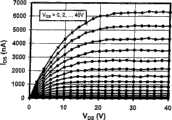
图4是示出了图1所示晶体管结构的漏源电流(IDS)相对漏源电压(VDS)的曲线图,其是栅源电压(VGS)的函数(栅源电压从+40V(曲线顶)到+2V以2V的步长进行变化);Figure 4 is a graph showing the drain-source current (IDS ) versus the drain-source voltage (VDS ) for the transistor structure shown in Figure 1 as a function of the gate-source voltage (VGS ) (gate-source voltage from +40V (curve top) to +2V with a step size of 2V);
图5示出了图1所示晶体管结构在三个多种漏源电压处的IDS-VGS特性曲线;Figure 5 shows the IDS -VGS characteristic curves of the transistor structure shown in Figure 1 at three various drain-source voltages;
图6示出了图1所示晶体管结构使用透明薄膜电阻负载(R=70MΩ)和VDD=40V的供电电压时的反相传输特性曲线;FIG. 6 shows the reverse phase transfer characteristic curve when the transistor structure shown in FIG. 1 uses a transparent thin-film resistive load (R=70MΩ) and a power supply voltage of VDD =40V;
图7示出了通过图1所示晶体管结构的源极或漏极部分的光透射特性的图;FIG. 7 shows a graph of light transmission characteristics through a source or drain portion of the transistor structure shown in FIG. 1;
图8是此处公开的晶体管结构的第四实施例的剖面图;8 is a cross-sectional view of a fourth embodiment of the transistor structure disclosed herein;
图9是此处公开的晶体管结构的第五实施例的剖面图;9 is a cross-sectional view of a fifth embodiment of the transistor structure disclosed herein;
图10是此处公开的晶体管结构的第六实施例的剖面图;10 is a cross-sectional view of a sixth embodiment of the transistor structure disclosed herein;
图11是包括此处公开的晶体管结构的AMLCD的单元电路示例的示意图;11 is a schematic diagram of an example unit circuit of an AMLCD including the transistor structure disclosed herein;
图12是包括此处公开的晶体管结构的动态随机存取存储器(DRAM)单元电路示例的示意图;12 is a schematic diagram of an example of a dynamic random access memory (DRAM) cell circuit including the transistor structure disclosed herein;
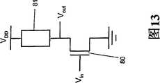
图13是包括此处公开的晶体管结构的逻辑反相器示例的示意图;13 is a schematic diagram of an example logic inverter including the transistor structures disclosed herein;
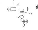
图14是包括此处公开的晶体管结构的反向放大器电路示例的示意图。14 is a schematic diagram of an example of an inverting amplifier circuit including the transistor structures disclosed herein.
几个实施例的详细描述Detailed description of several embodiments
为便于理解,下文详细描述了此处使用的术语:For ease of understanding, the terms used here are described in detail below:
“增强型晶体管”表示在零栅压时在源极和漏极之间存在相对于导通电流是可忽略的截止电流的晶体管。换言之,该晶体管器件是“常截止的”。相反地,耗尽型晶体管是“常导通的”,表示在零栅压时在源极和漏极之间流动的电流比大于基本可忽略的电流。"Enhancement mode transistor" means a transistor having a negligible off current relative to the on current between the source and drain at zero gate voltage. In other words, the transistor device is "normally off". Conversely, a depletion-mode transistor is "normally on," meaning that at zero gate voltage a greater than essentially negligible ratio of current flows between source and drain.
“栅极”通常指用于晶体管电路配置环境中的三端FET的绝缘栅端。"Gate" generally refers to the insulated gate terminal of a three-terminal FET used in the context of a transistor circuit configuration.
“基本绝缘”可以包括绝缘材料(例如,具有大于约1010Ω-cm的电阻率的材料)和半绝缘材料(例如,具有约103Ω-cm至1010Ω-cm的电阻率的材料)。"Substantially insulating" may include insulating materials (e.g., materials having a resistivity greater than about1010 Ω-cm) and semi-insulating materials (e.g., materials having a resistivity of about103 Ω-cm to1010 Ω-cm ).
“基本透明”通常指在电磁频谱的可见光部分(和/或在某些变型中的红外光部分)中不吸收大量光的材料或者结构。"Substantially transparent" generally refers to a material or structure that does not absorb substantial amounts of light in the visible portion (and/or in some variations, the infrared portion) of the electromagnetic spectrum.
“垂直”指基本上与衬底的表面垂直。"Perpendicular" means substantially perpendicular to the surface of the substrate.
前面的术语描述是仅是为帮助读者而提供的,而不应被解释为具有小于本领域的普通技术人员所理解的范围,或者其不应限制附属权利要求的范围。The preceding description in terms is provided merely to assist the reader, and should not be construed as having a scope less than that understood by those of ordinary skill in the art, or that it should not limit the scope of the appended claims.
此处公开的是增强型的场效应晶体管,其中晶体管结构的至少一部分是基本透明的。还公开了包括该晶体管的器件和用于制造该晶体管的方法。Disclosed herein are enhancement mode field effect transistors in which at least a portion of the transistor structure is substantially transparent. Devices including the transistors and methods for fabricating the transistors are also disclosed.
该晶体管的一个变型包括沟道层,其包括选自ZnO、SnO2或者In2O3中的基本绝缘的、基本透明的材料。包括基本透明材料的栅绝缘层位于与沟道层相邻的位置上,由此限定了沟道层/栅绝缘层界面。该晶体管还包括能够将电子注入到沟道层中使之积累在沟道层/栅绝缘层界面的源极,以及能够从沟道层中抽取电子的漏极。A variation of the transistor includesa channel layer comprising a substantially insulating, substantially transparent material selected from ZnO,SnO2 , orIn2O3 . A gate insulating layer comprising a substantially transparent material is positioned adjacent to the channel layer, thereby defining a channel layer/gate insulating layer interface. The transistor also includes a source capable of injecting electrons into the channel layer to accumulate at the channel layer/gate insulating layer interface, and a drain capable of extracting electrons from the channel layer.
该晶体管的第二变型包括沟道层,其包括选自基本绝缘的ZnO、基本绝缘的SnO2或者基本绝缘的In2O3中的基本透明的材料,该基本绝缘的ZnO、基本绝缘的SnO2或者基本绝缘的In2O3是通过退火工艺生产的。栅绝缘层位于与沟道层相邻的位置上,并且包括基本透明的材料。该晶体管还包括源极、漏极和栅电极。A second variant of the transistor includes a channel layer comprising a substantially transparent material selected from substantially insulating ZnO, substantially insulating SnO2 , or substantially insulating In2 O3 , the substantially insulating ZnO, substantially insulating SnO2 or substantially insulating In2 O3 is produced by an annealing process. The gate insulating layer is located adjacent to the channel layer and includes a substantially transparent material. The transistor also includes source, drain and gate electrodes.
用于制造该晶体管的方法包括:提供栅绝缘层,将ZnO、SnO2或者In2O3淀积在栅绝缘层的至少部分表面上,和使ZnO、SnO2或者In2O3在氧化环境中在约300至约1000℃的温度下退火约1分钟至2小时。The method for manufacturing the transistor includes: providing a gate insulating layer, depositing ZnO, SnO2 or In2 O3 on at least part of the surface of the gate insulating layer, and exposing the ZnO, SnO2 or In2 O3 to an oxidizing environment anneal at a temperature of about 300 to about 1000° C. for about 1 minute to 2 hours.
该晶体管可以作为联接到至少一个显示元件的开关包括在光电显示器件中。另一公开的器件是基本透明的动态随机存取存储单元,其包括联接到该晶体管的基本透明的电容器。该晶体管的另一应用是在基本透明的反相器中,其中该晶体管联接到负载器件。The transistor may be included in an optoelectronic display device as a switch coupled to at least one display element. Another disclosed device is a substantially transparent dynamic random access memory cell including a substantially transparent capacitor coupled to the transistor. Another application of the transistor is in a substantially transparent inverter, where the transistor is coupled to a load device.
通常,晶体管结构包括衬底、栅电极、栅绝缘层、沟道层、源极和漏极。沟道层可以位于与栅绝缘层相邻的位置,由此沟道层的表面与栅绝缘层的表面相接近。沟道层表面和栅绝缘层表面的接触区域在此处被称为沟道层/栅绝缘层界面。在示例性的构造中,沟道层的绝缘材料与栅绝缘层的材料不同,并且沟道层/栅绝缘层界面限定了离散的材料边界。Generally, a transistor structure includes a substrate, a gate electrode, a gate insulating layer, a channel layer, a source and a drain. The channel layer may be located adjacent to the gate insulating layer such that the surface of the channel layer is close to the surface of the gate insulating layer. The contact area of the surface of the channel layer and the surface of the gate insulating layer is referred to herein as a channel layer/gate insulating layer interface. In an exemplary configuration, the insulating material of the channel layer is different from the material of the gate insulating layer, and the channel layer/gate insulating layer interface defines discrete material boundaries.
该晶体管结构的实施例的特征是,沟道层/栅绝缘层界面限定了导电沟道,用于使电子从源极流向漏极。换言之,该晶体管可被归类为“表面沟道”或者“界面沟道”器件。施加的栅电压促使电子在沟道层/栅绝缘层界面区域积累。此外,施加的电压增强了从源极到沟道层/栅绝缘层界面的电子注入,并且增强了由漏极对其进行的电子抽取。An embodiment of the transistor structure is characterized in that the channel layer/gate insulating layer interface defines a conductive channel for electrons to flow from the source to the drain. In other words, the transistor can be classified as a "surface channel" or "interface channel" device. The applied gate voltage promotes the accumulation of electrons in the channel layer/gate insulating layer interface region. In addition, the applied voltage enhances electron injection from the source to the channel layer/gate insulating layer interface and enhances electron extraction therefrom by the drain.
该晶体管结构的另一特征是,该沟道层和栅绝缘层的构造或者组合的所选实施例在电磁频谱的可见光部分上(和/或在某些变型中的红外光部分)呈现出至少约90%的光透射率,更特别地,具有至少约95%的透射率。取决于所需的晶体管最终应用,该结构的每一个额外部件(即,衬底、栅电极、源/漏端)可被选择为不透明的或者基本透明的。在某些实施例中,该晶体管结构整体可以在电磁频谱的可见光部分上(和/或在某些变型中的红外光部分)呈现出至少约50%的光透射率,更特别地是至少约70%的光透射率,而最特别的是至少约90%的光透射率。Another feature of the transistor structure is that selected embodiments of the configuration or combination of the channel layer and gate insulating layer exhibit at least A light transmission of about 90%, more particularly, having a transmission of at least about 95%. Each additional component of the structure (ie, substrate, gate electrode, source/drain terminals) can be chosen to be opaque or substantially transparent depending on the desired end application of the transistor. In certain embodiments, the transistor structure as a whole may exhibit a light transmission of at least about 50 percent over the visible portion of the electromagnetic spectrum (and/or, in some variations, the infrared portion), more particularly at least about 70% light transmission, and most particularly at least about 90% light transmission.
此处公开的FET的进一步的特征是,其可以容易地作为薄膜晶体管(TFT)而被制造。例如,可以使用相对低的工艺温度(例如,不超过约800℃),并且不需要离子注入工艺来设置沟道阈值电压和在该FET结构的某些变型中限定源极和漏极接触。该TFT典型地在结合光电器件使用时是非常有用的,如下文所详细描述的。A further feature of the FETs disclosed herein is that they can be easily fabricated as thin film transistors (TFTs). For example, relatively low process temperatures (eg, no more than about 800° C.) can be used, and ion implantation processes are not required to set the channel threshold voltage and define source and drain contacts in certain variations of the FET structure. Such TFTs are typically very useful when used in conjunction with optoelectronic devices, as described in detail below.
沟道层典型地由基本绝缘的材料制成,其也是基本透明的。由于沟道层由基本绝缘的材料制成,因此可用在沟道层的体块部分中固有的电子量是可忽略的。此外,基本绝缘的沟道层可以提供固有的电绝缘,用于多个器件共享连续的沟道层膜(具有限定每个器件的被构图的栅电极、源电极和漏电极)。该固有的器件绝缘意味着,由于呈现出来的沟道层/栅绝缘层处的电导率仅低于被构图的栅电极,因此沟道层膜的构图不是必需的。The channel layer is typically made of a substantially insulating material that is also substantially transparent. Since the channel layer is made of a substantially insulating material, the inherent amount of electrons available in the bulk portion of the channel layer is negligible. In addition, the substantially insulating channel layer can provide inherent electrical isolation for multiple devices to share a continuous channel layer film (with patterned gate, source, and drain electrodes defining each device). This inherent device isolation means that patterning of the channel layer film is not necessary since the conductivity at the channel layer/gate insulating layer is only present to be lower than that of the patterned gate electrode.
用于该沟道层的说明性材料包括ZnO、SnO2和In2O3。绝缘的ZnO、SnO2和In2O3可以通过退火工艺生产,特定地是快速热退火(RTA)工艺制造。该绝缘的ZnO、SnO2和In2O3典型地呈现出具有小于约5eV的能带间隙。Illustrative materials for the channel layer include ZnO, SnO2 and In2 O3 . Insulating ZnO, SnO2 and In2 O3 can be produced by an annealing process, in particular a rapid thermal annealing (RTA) process. The insulating ZnO, SnO2 and In2 O3 typically exhibit band gaps of less than about 5 eV.
例如,可以淀积ZnO层(例如通过溅射、化学气相淀积、旋涂、物理气相淀积、气相外延、分子束外延等等)并且随后使其在基本氧化的环境中在约300至约1000℃的温度下(特别是约700至约800℃)经历约1分钟至约2小时(更特别的是约1分钟至约1小时,在某些情况中是约1分钟至约5分钟)的退火工艺。尽管不受任何理论的约束,但是可以相信,该工艺将导致在ZnO层中并入更多的氧,由此降低了氧缺位浓度或者氧缺乏程度。ZnO中的氧缺位或者氧缺乏可以致使其是n型的并且是可导电的。在诸如氩的惰性气体环境中的高温(即,至少约700℃)退火也可以产生绝缘ZnO。尽管不受任何理论的约束,但是该较高温度的退火可以改善ZnO的结晶度,由此改善了电子输运特性。可以掺杂该绝缘ZnO,也可以不进行掺杂。如果进行了掺杂,则可以通过使用受主掺杂剂的置换掺杂来增加ZnO的电阻率,该受主掺杂剂诸如例如,N、Cu、Li、Na、K、Rb、P、As及其混合物。For example, a ZnO layer can be deposited (e.g., by sputtering, chemical vapor deposition, spin coating, physical vapor deposition, vapor phase epitaxy, molecular beam epitaxy, etc.) At a temperature of 1000°C (especially about 700 to about 800°C) for about 1 minute to about 2 hours (more specifically about 1 minute to about 1 hour, in some cases about 1 minute to about 5 minutes) annealing process. While not being bound by any theory, it is believed that this process will result in more oxygen being incorporated in the ZnO layer, thereby reducing the concentration of oxygen vacancies, or degree of oxygen deficiency. Oxygen vacancies or lack of oxygen in ZnO can render it n-type and conductive. High temperature (ie, at least about 700°C) annealing in an inert gas environment such as argon can also produce insulating ZnO. While not being bound by any theory, this higher temperature anneal may improve the crystallinity of ZnO, thereby improving electron transport properties. This insulating ZnO may be doped or not. If doped, the resistivity of ZnO can be increased by displacement doping with acceptor dopants such as, for example, N, Cu, Li, Na, K, Rb, P, As and mixtures thereof.
相似地,可以淀积SnO2层(例如通过溅射、化学气相淀积、旋涂、物理气相淀积、气相外延、分子束外延等等)并且随后使其在基本氧化的环境中在约300至约1000℃的温度下(特别是约700至约900℃的温度下)经历约1分钟至约2小时(更特别的是约1分钟至约1小时,在某些情况中是约1分钟至约5分钟)的退火工艺。尽管不受任何理论的约束,但是可以相信,该工艺将导致在SnO2层中并入更多的氧,由此降低了氧缺位浓度或者氧缺乏程度。SnO2中的氧缺位或者氧缺乏可以致使其是n型的并且是可导电的。诸如氩的惰性气体环境中的高温(即,大于约700℃)退火也可以产生绝缘SnO2。尽管不受任何理论的约束,但是该较高温度的退火可以改善SnO2的结晶度,由此改善了电子输运特性。可以通过使用受主掺杂剂的置换掺杂来增加SnO2的电阻率,该受主掺杂剂诸如例如,Al、In、Ga、Bi、B、La、Sc、Y、Lu、Er、Ho、N、P、As及其混合物。Similarly, a layer ofSnO2 can be deposited (e.g., by sputtering, chemical vapor deposition, spin coating, physical vapor deposition, vapor phase epitaxy, molecular beam epitaxy, etc.) to a temperature of about 1000° C. (especially a temperature of about 700 to about 900° C.) for about 1 minute to about 2 hours (more particularly about 1 minute to about 1 hour, in some cases about 1 minute to about 5 minutes) annealing process. While not being bound by any theory, it is believed that this process will result in the incorporation of more oxygen in theSnO2 layer, thereby reducing the concentration of oxygen vacancies, or degree of oxygen deficiency. Oxygen vacancies, or lack of oxygen, inSnO2 can render it n-type and conductive. High temperature (ie, greater than about 700° C.) anneals in an inert gas environment such as argon can also produce insulating SnO2 . While not being bound by any theory, this higher temperature anneal can improve the crystallinity of SnO2 , thereby improving the electron transport properties. The resistivity ofSnO2 can be increased by displacement doping with acceptor dopants such as, for example, Al, In, Ga, Bi, B, La, Sc, Y, Lu, Er, Ho , N, P, As and their mixtures.
同样相似地,可以淀积In2O3层(例如通过溅射、化学气相淀积、旋涂、物理气相淀积、气相外延、分子束外延等等)并且随后使其在基本氧化的环境中在约300至约1000℃的温度下(特别是约700至约900℃的温度下)经历约1分钟至约2小时(更特别的是约1分钟至约1小时,在某些情况中是约1分钟至约5分钟)的退火工艺。尽管不受任何理论的约束,但是可以相信,该工艺将导致在In2O3层中并入更多的氧,由此降低了氧缺位浓度或者氧缺乏程度。In2O3中的氧缺位或者氧缺乏可以致使其是n型的并且是可导电的。诸如氩的惰性气体环境中的高温(即,大于约700℃)退火也可以产生绝缘In2O3。尽管不受任何理论的约束,但是该较高温度的退火可以改善In2O3的结晶度,由此改善了电子输运特性。可以通过使用受主掺杂剂的置换掺杂来增加In2O3的电阻率,该受主掺杂剂诸如例如,Be、Mg、Ca、Sr、Ba、N、P、As、Zn、Cd及其混合物。Also similarly, a layer of In2 O3 can be deposited (e.g. by sputtering, chemical vapor deposition, spin coating, physical vapor deposition, vapor phase epitaxy, molecular beam epitaxy, etc.) At a temperature of about 300 to about 1000°C (especially at a temperature of about 700 to about 900°C) for about 1 minute to about 2 hours (more specifically about 1 minute to about 1 hour, in some cases about 1 minute to about 5 minutes) annealing process. While not being bound by any theory, it is believed that this process will result in more oxygen being incorporated in the In2 O3 layer, thereby reducing the concentration of oxygen vacancies, or degree of oxygen deficiency. Oxygen vacancies or lack of oxygen in In2 O3 can render it n-type and conductive. High temperature (ie, greater than about 700° C.) annealing in an inert gas environment such as argon can also produce insulating In2 O3 . While not being bound by any theory, this higher temperature anneal may improve the crystallinity ofIn2O3 , thereby improving the electron transportproperties . The resistivity ofIn2O3 can be increased by displacement doping with acceptor dopants such as, for example, Be, Mg, Ca, Sr,Ba , N, P, As, Zn, Cd and mixtures thereof.
根据特定的实施例,ZnO、SnO2或者In2O3层可以在包括至少一种溅射气体和至少一种膜调整气体的环境中通过溅射进行淀积。该膜调整气体可以是任何能够通过在原子或者亚原子水平上并入到膜中来增加膜电阻率的气体。例如,膜调整气体可以是其自身分子、原子或者离子并入到膜中使得如上文所述占据了膜中的氧缺位或者缺陷的氧化气体。另一种膜调整气体可以是其自身分子、原子或者离子并入到膜中使得其增加了膜电阻率的掺杂剂气体。说明性的溅射气体包括Ar、Ne及其混合物。说明性的氧化气体包括O2、N2O及其混合物。说明性的掺杂剂气体包括N2、NH3和其他包括上文列出的掺杂剂类型的气体。在溅射环境中的气体浓度可以取决于所需的膜特性而进行变化。例如,氧化气体的浓度可以在约0至约50的体积百分比的范围内变化。掺杂剂气体的浓度可以在约0至约50的体积百分比的范围内变化。溅射气体的浓度可以在约0至约100的体积百分比的范围内变化。溅射条件也可以取决于所需的膜特性而进行变化。例如,温度可以从约室温至600℃的范围内变化,并且压力可以在约1mTorr至约50mTorr的范围中变化。在特定的示例中,可以在包括80体积百分比的Ar、10体积百分比的N2和10体积百分比的O2的环境中,通过溅射来淀积未掺杂的ZnO靶。According to a particular embodiment, the ZnO, SnO2 or In2 O3 layer may be deposited by sputtering in an environment comprising at least one sputtering gas and at least one film conditioning gas. The film modifying gas can be any gas capable of increasing the film resistivity by incorporation into the film at the atomic or subatomic level. For example, the membrane conditioning gas may be an oxidizing gas that incorporates its own molecules, atoms, or ions into the membrane such that oxygen vacancies or defects in the membrane are occupied as described above. Another film modifying gas may be a dopant gas that incorporates its own molecules, atoms, or ions into the film such that it increases the film resistivity. Illustrative sputtering gases include Ar, Ne, and mixtures thereof. Illustrative oxidizing gases includeO2 ,N2O , and mixtures thereof. Illustrative dopant gases includeN2 ,NH3 , and other gases including the dopant types listed above. The gas concentration in the sputtering environment can be varied depending on the desired film properties. For example, the concentration of the oxidizing gas may range from about 0 to about 50 volume percent. The concentration of the dopant gas may vary in the range of about 0 to about 50 volume percent. The concentration of the sputtering gas can vary in the range of about 0 to about 100 volume percent. Sputtering conditions can also be varied depending on the desired film properties. For example, the temperature may range from about room temperature to 600° C., and the pressure may range from about 1 mTorr to about 50 mTorr. In a specific example, an undoped ZnO target may be deposited by sputtering in an environment including 80 volume percent Ar, 10 volume percentN2 , and 10 volume percentO2 .
沟道层的厚度可以变化,并且可以根据特定的示例,在约10至约500nm的范围中变化。沟道长度也可以变化,并且可以根据特定的示例,在约1,000至约100,000nm的范围中变化。The thickness of the channel layer can vary, and can range from about 10 to about 500 nm, according to a particular example. The channel length can also vary, and can range from about 1,000 to about 100,000 nm, depending on the particular example.
栅绝缘层可以由任何呈现出栅绝缘体所需的绝缘特性的材料制成,特别是基本透明的材料。栅绝缘体材料典型地呈现出大于约5eV的能带间隙。说明性的材料包括基本透明的材料,诸如铝钛氧化物(Al2O3/TiO2)、Al2O3、MgO、SiO2、氮化硅和氮氧化硅。基本透明材料的一个特殊的示例是通过原子层淀积生长的铝钛氧化物。栅绝缘层的厚度可以变化,并且可以根据特定的示例,在约10至约300nm的范围中变化。可以通过诸如化学气相淀积、溅射、原子层淀积或者蒸发的技术将栅绝缘层引入到该结构中。The gate insulating layer may be made of any material exhibiting the required insulating properties of a gate insulator, in particular a substantially transparent material. Gate insulator materials typically exhibit an energy band gap greater than about 5 eV. Illustrative materials include substantially transparent materials such as aluminum titanium oxide (Al2 O3 /TiO2 ), Al2 O3 , MgO, SiO2 , silicon nitride, and silicon oxynitride. A particular example of a substantially transparent material is aluminum titanium oxide grown by atomic layer deposition. The thickness of the gate insulating layer may vary, and may vary in the range of about 10 to about 300 nm according to a particular example. The gate insulating layer can be introduced into the structure by techniques such as chemical vapor deposition, sputtering, atomic layer deposition or evaporation.
源/漏端是指FET的极端,在电场的影响下在该极端之间出现传导。设计者通常基于FET在电路中操作时施加到极端的电压来将特定的源/漏端指定为“源极”或者“漏极”。源极和漏极可以由任何适当的导电材料制成,诸如n型材料。源极和漏极材料可被选择为不透明的材料或者基本透明的材料。说明性的材料包括透明的n型导体,诸如氧化铟锡(ITO)、ZnO、SnO2或者In2O3,或者包括不透明的材料,诸如Al、Cu、Au、Pt、W、Ni或者Ti。对于源极和漏极特别有用的材料是那些能够向沟道层绝缘材料注入(和抽取)电子的材料。该电子注入材料的实例包括氧化铟锡、LaB6和ZnO:Al。Source/Drain refers to the extremes of a FET between which conduction occurs under the influence of an electric field. Designers typically designate a particular source/drain terminal as "source" or "drain" based on the extreme voltages to which the FET is applied when operating in the circuit. The source and drain can be made of any suitable conductive material, such as n-type material. The source and drain materials can be selected to be opaque or substantially transparent. Illustrative materials include transparent n-type conductors, such as indium tin oxide (ITO), ZnO,SnO2 , orIn2O3 , or opaque materials, such as Al, Cu, Au, Pt, W, Ni, or Ti. Particularly useful materials for the source and drain electrodes are those capable of injecting (and extracting) electrons into the channel layer insulating material. Examples of the electron injection material include indium tin oxide, LaB6 and ZnO:Al.
可以通过诸如化学气相淀积、溅射、蒸发和/或通过扩散或离子注入掺杂沟道层材料的技术,将源极和漏极引入到该结构中。可以制造源极和漏极使得它们在几何上是几何对称的或者是不对称的。Source and drain electrodes may be introduced into the structure by techniques such as chemical vapor deposition, sputtering, evaporation and/or doping of the channel layer material by diffusion or ion implantation. The source and drain can be fabricated such that they are geometrically symmetrical or asymmetrical in geometry.
栅电极可以由任何适当的传导材料制成。栅电极材料可被选择为不透明的材料或者基本透明的材料。说明性的栅电极材料包括透明的n型导体,诸如氧化铟锡(ITO)、ZnO、SnO2或者In2O3,或者包括不透明的材料,诸如Al、Cu、Au、Pt、W、Ni或者Ti。栅电极的厚度可以变化,并且可以根据特定的示例,在约50至约1000nm的范围中变化。可以通过诸如化学气相淀积、溅射、蒸发和/或掺杂的技术将栅电极引入到该结构中。The gate electrode can be made of any suitable conductive material. The gate electrode material can be selected to be an opaque material or a substantially transparent material. Illustrative gate electrode materials include transparent n-type conductors such as indium tin oxide (ITO), ZnO, SnO2 , or In2 O3 , or opaque materials such as Al, Cu, Au, Pt, W, Ni, or Ti. The thickness of the gate electrode can vary, and can range from about 50 to about 1000 nm, according to a particular example. The gate electrode may be introduced into the structure by techniques such as chemical vapor deposition, sputtering, evaporation and/or doping.
如此处所使用的,“衬底”是指作为基础工件的物理物体,其通过多种工艺操作被转化为所需的微电子构造。衬底还可以指晶片。晶片可以由半导体材料、非半导体材料或者半导体材料和非半导体材料的组合制成。衬底可以由任何适当的材料制成。衬底材料可被选择为不透明的材料或者基本透明的材料。说明性的衬底材料包括玻璃和硅。衬底的厚度可以变化,并且可以根据特定的示例,在约100μm至约1cm的范围中变化。As used herein, "substrate" refers to the physical object that is the base workpiece that is transformed through a variety of process operations into a desired microelectronic configuration. A substrate may also refer to a wafer. Wafers may be made of semiconducting materials, non-semiconducting materials, or a combination of semiconducting and non-semiconducting materials. The substrate can be made of any suitable material. The substrate material can be chosen to be an opaque material or a substantially transparent material. Illustrative substrate materials include glass and silicon. The thickness of the substrate may vary, and may vary in the range of about 100 μm to about 1 cm according to a particular example.
可以以任何方式提供对栅电极、源极、漏极和衬底的电接触。例如,可以使用金属线、迹线、导线、互连、导体、信号路径和信号传播介质来提供所需的电气连接。上文列出的项通常是可互换的,并且按照从特殊到一般的顺序排列。通常是铝(Al)、铜(Cu)、或者Al和Cu的合金的金属线是提供用于联接或者互连电路的信号路径的导体。还可以使用除了金属以外的导体。Electrical contacts to the gate electrode, source, drain and substrate may be provided in any manner. For example, metal lines, traces, conductors, interconnects, conductors, signal paths, and signal propagation media may be used to provide the required electrical connections. The items listed above are generally interchangeable and are listed in order from specific to general. Metal wires, typically aluminum (Al), copper (Cu), or an alloy of Al and Cu, are conductors that provide signal paths for coupling or interconnecting circuits. Conductors other than metals may also be used.
说明性的n沟道晶体管的操作涉及,向栅电极施加正电压,将源极接地,和向漏极施加正电压。例如,在操作期间向栅电极和漏极施加约5至约40V的电压。阈值电压可以在约1至约20V的范围中变化。电子从源极沿在沟道层/栅绝缘层界面处产生的导电沟道通过漏极流出晶体管。电子在界面处的有效迁移率可以取决于特定的结构而变化,但是可以在一定的范围中变化,例如约0.05至约20cm2V-1s-1。由于该晶体管是增强型晶体管,因此简单地移除施加在栅电极上的正电压可以使晶体管截止。Operation of the illustrative n-channel transistor involves applying a positive voltage to the gate electrode, grounding the source, and applying a positive voltage to the drain. For example, a voltage of about 5 to about 40V is applied to the gate electrode and the drain during operation. The threshold voltage can vary in the range of about 1 to about 20V. Electrons flow out of the transistor from the source through the drain along a conduction channel created at the channel layer/gate insulating layer interface. The effective mobility of electrons at the interface can vary depending on the particular structure, but can vary within a range, eg, about 0.05 to about 20 cm2 V−1 s−1 . Since this transistor is an enhancement mode transistor, simply removing the positive voltage applied to the gate electrode turns off the transistor.
此处公开的晶体管结构可被用于制造芯片、集成电路、单片器件,半导体器件和微电子器件。一个微电子器件的示例是光电器件。说明性的光电器件是有源矩阵液晶显示器(AMLCD)。The transistor structures disclosed herein can be used in the fabrication of chips, integrated circuits, monolithic devices, semiconductor devices, and microelectronic devices. An example of a microelectronic device is an optoelectronic device. An illustrative optoelectronic device is an active matrix liquid crystal display (AMLCD).
一个示例器件是光电显示器件,其包括具有电极和淀积在电极之间的光电材料的元件。透明晶体管的连接电极可以连接到显示元件的电极,而开关元件的显示元件至少在一部分上相互重叠。这里,光电显示元件被理解为其光学特性在电气量(诸如电流和电压)的作用下发生改变的显示元件,诸如例如,通常被称为液晶显示器(LCD)的元件。此处详细描述的透明晶体管作为以高频来开关显示元件来说是足够快的,使得可以使用透明晶体管作为液晶显示器中的开关元件。该显示元件在电气方面可以被当成电容器,其通过伴随的透明晶体管而进行充电和放电。光电显示器件可以包括许多显示元件,每一个显示元件都具有其自己的透明晶体管(例如,排列在矩阵中)。可以如,例如,Kim,“Thin-Film-Transistor Device Design”,Information Display2/02,p.26(2002)中所描述的,为LCD器件排列该透明晶体管。An example device is an optoelectronic display device comprising elements having electrodes and optoelectronic material deposited between the electrodes. The connection electrode of the transparent transistor may be connected to an electrode of the display element, and the display elements of the switching element overlap each other at least in part. Here, an optoelectronic display element is understood to be a display element whose optical properties are changed under the action of electrical quantities such as current and voltage, such as, for example, what is commonly referred to as a liquid crystal display (LCD). The transparent transistors described in detail here are fast enough to switch display elements at high frequencies so that transparent transistors can be used as switching elements in liquid crystal displays. The display element can be regarded electrically as a capacitor, which is charged and discharged via an accompanying transparent transistor. An optoelectronic display device may comprise a number of display elements, each display element having its own transparent transistors (eg arranged in a matrix). The transparent transistor can be arranged for an LCD device as described, for example, in Kim, "Thin-Film-Transistor Device Design",
在图11中示出了AMLCD单元电路的一个特定示例。该AMLCD单元电路包括如此处描述的晶体管60和与之电气联接的LCD像素61。晶体管60和LCD像素61一起形成了晶体管/像素单元62。在所示配置中,晶体管60通过漏电极电气联接到LCD像素61。晶体管60的栅电极电气联接到接收用于晶体管60的开/关输入的行或者控制线63。晶体管60的源电极电气联接到接收用于控制LCD像素61的信号的列或者数据线64。A specific example of an AMLCD cell circuit is shown in FIG. 11 . The AMLCD cell circuit includes a transistor 60 as described herein and an LCD pixel 61 electrically coupled thereto. Transistor 60 and LCD pixel 61 together form transistor/pixel unit 62 . In the configuration shown, transistor 60 is electrically coupled to LCD pixel 61 through a drain electrode. The gate electrode of transistor 60 is electrically coupled to a row or control line 63 that receives an on/off input for transistor 60 . The source electrode of transistor 60 is electrically coupled to a column or data line 64 that receives signals for controlling LCD pixels 61 .
可以使用此处示出的晶体管结构的微电子器件的其他示例包括反相器、模拟放大器和单管动态随机存取存储(DRAM)单元以及相似的器件。Other examples of microelectronic devices that may use the transistor structures shown here include inverters, analog amplifiers, and single-transistor dynamic random access memory (DRAM) cells, and similar devices.
例如,透明的增强型晶体管,在其源极连接至透明电容器的一个极端,而电容器的另一极端接地时,构成了透明的单管动态随机存取存储(DRAM)单元。在该DRAM单元中,信息作为电容器上的电荷存储,该增强型晶体管用作存取晶体管,其控制电容器的电荷状态。通常在该DRAM单元中,可忽略的电容器电荷量和伴随的小的电容器电压表示逻辑“0”。相反地,通过对电容器充电,由此增加电容器电压直到其达到供电电压,获得了逻辑“1”。For example, a transparent enhancement-mode transistor, with its source connected to one terminal of a transparent capacitor and the other terminal of the capacitor to ground, forms a transparent single-transistor dynamic random access memory (DRAM) cell. In the DRAM cell, information is stored as charge on a capacitor, and the enhancement mode transistor acts as an access transistor, which controls the charge state of the capacitor. Typically in this DRAM cell, a negligible amount of capacitor charge and an accompanying small capacitor voltage represent a logic "0". Conversely, a logic "1" is obtained by charging the capacitor, thereby increasing the capacitor voltage until it reaches the supply voltage.
此处描述的完整的DRAM单元或者其一部分是透明的。可以使用多种技术来完成制造透明电容器并且将其连接至透明晶体管以实现DRAM单元。特定地,通过将使用诸如Al2O3或者SiO2材料将透明绝缘层夹在两个使用诸如氧化铟锡、ZnO或者SnO2材料的透明导体之间,可以构建透明电容器。Complete DRAM cells or portions thereof described herein are transparent. Fabricating the transparent capacitor and connecting it to the transparent transistor to implement the DRAM cell can be done using a variety of techniques. Specifically, a transparent capacitor can be constructed by sandwiching a transparent insulating layer using a material such asAl2O3 orSiO2 between two transparent conductors using a material such asindium tin oxide, ZnO orSnO2 .
在图12中示出了DRAM单元电路的一个特定的示例。该DRAM单元电路包括如此处描述的晶体管70和与之电气联接的存储电容器71。晶体管70和存储电容器71一起形成了晶体管/电容器单元72。在所示配置中,晶体管70通过漏电极电气联接到存储电容器71。晶体管70的栅电极电气联接到接收用于晶体管70的开/关输入的行或者写入线73。晶体管70的源电极电气联接到接收用于控制存储电容器71所存储信息的信号的列或者数据线74。A specific example of a DRAM cell circuit is shown in FIG. 12 . The DRAM cell circuit includes a
图1至3和图8至10中示出了特定的晶体管结构的说明性示例。下文特定的示例是用于说明性的目的,并且不应被理解为限制附属权利要求的范围。在图1至3和图8至10中,除非特别说明,相似的参考数字表示相似的元件。Illustrative examples of specific transistor structures are shown in FIGS. 1 to 3 and 8 to 10 . The specific examples below are for illustrative purposes and should not be construed as limiting the scope of the appended claims. In FIGS. 1 to 3 and FIGS. 8 to 10 , like reference numerals designate like elements unless otherwise specified.
图1figure 1
示出了TFT结构1,其被制造在1英寸×1英寸厚的复合衬底上。该平台包括200nm厚的玻璃衬底2、涂布在衬底2上的氧化铟锡(ITO)栅电极3和200nm厚的铝钛氧化物绝缘层4。A
ZnO沟道和ITO源/漏电极膜通过在10-4Torr的Ar/O2(80%/20%)中的离子束溅射进行淀积;衬底在淀积过程中未加热。使用阴影掩模来限定ZnO沟道层5(100nm厚)、ITO源电极6(300nm厚)和ITO漏电极7(300nm厚)。得到的结构限定了沟道层/栅绝缘层界面8。紧接在用于去除从暴露表面吸收杂质的ZnO和ITO淀积之前,在Ar中的300℃快速热退火(RTA)获得了膜质量的明显改善(特别用于ITO膜)。在淀积ZnO层之后,使用RTA(典型地在O2或者Ar中,600至800℃)增加ZnO沟道的电阻率并且改善沟道层/栅绝缘层界面8的电气质量。在ITO源/漏电极淀积之后,使用O2中300℃的RTA增加ITO层的透明度。在晶体管结构1中,将源/漏电极6和7安置在沟道层5的顶表面(在垂直视角上),并且将栅电极5和沟道层5分布安置在栅绝缘层4的相对表面上。因此,结构1允许在ITO源/漏电极6和7的淀积和处理之前,进行ZnO沟道层5的高温处理。如下文所述评估了TFT结构1的某些电气和物理特性,并且在图4至7中进行了说明。ZnO channel and ITO source/drain electrode films were deposited by ion beam sputtering in Ar/O2 (80%/20%) at 10−4 Torr; the substrate was not heated during deposition. A shadow mask was used to define the ZnO channel layer 5 (100 nm thick), the ITO source electrode 6 (300 nm thick) and the ITO drain electrode 7 (300 nm thick). The resulting structure defines a channel layer/gate insulating
通过参考图4,获得了n沟道增强型行为,这是基于这一事实而声明的,即需要超过约~15V(阈值)的正栅压来获得可测量的漏源电流。该IDS-VDS曲线呈现出了原型FET的特征;特别重要的是,这些曲线在大的漏电压处是平坦的(即,它们呈现“硬”饱和)。所使用的漏电压和栅电压相比于传统的FET是相当大的;通过简单地减小栅绝缘体的厚度,可以将栅电压和漏电压减小到典型FET操作所期望的范围(即~5至10V)。在TFT结构1中,由于被优化的用于电致发光显示应用,绝缘体厚度是~200nm;如果将另外的相同绝缘体重新调节为20nm的厚度,则栅电压和漏电压将以近似10的系数比例减小。By referring to Figure 4, n-channel enhancement-mode behavior is obtained, which is stated based on the fact that a positive gate voltage exceeding about ~15V (threshold) is required to obtain a measurable drain-source current. The IDS -VDS curves are characteristic of the prototype FETs; it is particularly important that these curves are flat at large drain voltages (ie, they exhibit "hard" saturation). The drain and gate voltages used are considerable compared to conventional FETs; by simply reducing the thickness of the gate insulator, the gate and drain voltages can be reduced to the range expected for typical FET operation (i.e. ~5 to 10V). In
结构1当前的IDS相当小(即图4中IDS(max)是约6μA)。在许多应用中更大的IDS可能是需要的。IDS的幅度由两个因素决定。一个是沟道电子的有效迁移率μeff(对于TFT结构1为约0.05至0.2cm2V-1s-1)。工艺/器件优化将导致μeff以系数比例约2至100进行增长,这将导致相应的IDS的增加。第二个因素是纵横比。TFT结构1的纵横比(栅极的物理宽度Z除以栅极的长度L)是约2(其中Z=2L=6000μm)。较大的纵横比将导致较大的电流IDS。The current IDS of
图5示出了TFT结构1在三个不同漏电压下的IDS-VGS特性。该图示出了在晶体管用作开关时,在“导通”和“截止”电流之间存在系数为105至106的差异。FIG. 5 shows the IDS -VGS characteristics of the
图6示出了TFT结构1在用作反相器时的传输特性。ZnO透明薄膜电阻(R=70MΩ)用作反相器无源负载,其中供电电压VDD=40V。从该曲线可以清楚地证明在15和30V之间有约15V的逻辑摆幅。这表明此处描述的透明TFT可以用作透明反相器。在其最简单的实现方案中,逻辑反相器包括两个组成部分;联接到负载器件的晶体管。该负载器件可以是电阻器,如本示例中所使用的。可替换地,耗尽型或者增强型晶体管也可以用作负载器件,典型地提供更好的性能。逻辑反相器的基本特性是它执行逻辑非运算,其中逻辑0(1)输入产生逻辑1(0)输出。由于反相器是用于实现透明数字电子电路的最基本的构成模块,所以如此处所述,成功的实现透明逻辑反相器是意义重大的。通过减小绝缘体厚度、减小物理尺寸和增加电流驱动能力(增加纵横比和有效迁移率)而进行的透明薄膜晶体管的优化将导致用于反相器操作的供电电压的明显降低。FIG. 6 shows the transfer characteristics of the
在图13中示出了逻辑反相器电路的一个特定示例。该逻辑反相器电路包括如此处描述的晶体管80。晶体管80的栅电极电气联接到电压输入端(Vin),晶体管80的源电极电气联接到地,并且晶体管80的漏电极电气联接到负载81和电源(VDD)。负载81可以是透明薄膜电阻或者透明薄膜晶体管。通过Vin使晶体管80导通或者截止来控制电路的电压输出(Vout)。A specific example of a logic inverter circuit is shown in FIG. 13 . The logic inverter circuit includes
透明晶体管还可以用于放大器应用中。例如,上文所述的反相器结构还可以用作简单的模拟反向放大器。通过在输入端施加适当的DC偏置,小的输入信号(叠加在DC偏置上)由反相器的传输特性进行放大。除了该简单的放大器配置,这些晶体管可以直接应用到任意的放大器配置中,但是由于这些器件低的迁移率,其最大操作频率极限相对要低。Transparent transistors can also be used in amplifier applications. For example, the inverter structure described above can also be used as a simple analog inverting amplifier. By applying an appropriate DC bias at the input, the small input signal (superimposed on the DC bias) is amplified by the transfer characteristics of the inverter. Apart from this simple amplifier configuration, these transistors can be directly applied to any amplifier configuration, but due to the low mobility of these devices, the maximum operating frequency limit is relatively low.
在图14中示出了反向放大器电路的一个特定示例。该反向放大器电路包括如此处描述的晶体管90。晶体管90的栅电极电气联接到电压输入信号(Vin)和DC偏置(Vbias)。晶体管90的源电极电气联接到地,并且晶体管90的漏电极电气联接到负载91和电源(VDD)。负载91可以是透明薄膜电阻或者透明薄膜晶体管。A specific example of an inverting amplifier circuit is shown in FIG. 14 . The inverting amplifier circuit includes
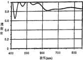
图7示出了TFT结构1通过源极6或者漏极7的光透射率(这里未示出的通过沟道的光透射率高于通过源极或者漏极的光透射率)。在电磁频谱的可见光部分(450-700nm)的平均透射率是约90%(通过沟道是约95%)。在视觉上,该透明TFT结构基本上是看不见的;在靠近观察时,玻璃衬底的略微染色是明显的。FIG. 7 shows the light transmittance of the
图2figure 2
在图2所示的另一透明TFT结构10的版本中,通过选择性地在ZnO沟道层13(100nm厚)的末端掺杂In(或者任何适当的n型掺杂剂),制造了源电极11(100nm厚)和漏电极12(100nm厚)。通过在淀积ZnO沟道膜之前,使用源/漏极阴影掩模由离子束溅射来淀积薄(约5nm)的ITO层,完成了这一操作。执行随后的高温(~600至800℃)退火步骤,用以扩散掺杂ZnO,由此形成了n型掺杂的源/漏区域11和12。扩散掺杂RTA还可用作用于ZnO的氧化RTA。ITO接触可以安置在源和漏区域上,用以提供更好的电气接触。衬底2、栅电极3、栅绝缘层4和沟道层/栅绝缘层界面8与图1中的相同。In another version of the
图3
在TFT结构的第三变型20中,在形成ZnO沟道层23(100nm厚)之前,淀积ITO源电极21(300nm厚)和ITO漏电极22(300nm厚)。随后ZnO沟道层23保形淀积在ITO源/漏电极21和22上。在ZnO的淀积之后,执行700℃的Ar退火,随后执行300℃的氧退火。衬底2、栅电极3、栅绝缘层4和沟道层/栅绝缘层界面8与图1中的相同。In a
图8Figure 8
图8示出了TFT结构的第四变型30。该TFT结构30包括玻璃衬底2,在其上安置有源电极35和漏电极36。所提供的沟道结构37包括位于源电极35和漏电极36之间并且与玻璃衬底2相邻的体块部分38。沟道结构37还包括界面部分39,其与体块部分38是一体的,并且分别置于栅绝缘层34同源电极35和漏电极36之间。界面部分39可以与每个源电极35或漏电极36的全部重叠,或者仅与其部分重叠。界面部分39和栅绝缘层34形成沟道层/栅绝缘层界面31,其限定了用于电子从源极流向漏极的导电沟道。栅电极33安置在栅绝缘层34的顶表面上(在垂直视角上)。换言之,栅电极33和沟道结构37提供在栅绝缘层34的相对表面上。Figure 8 shows a
例如,通过淀积和构图限定了源电极35和漏电极36的膜,可以制造该TFT结构30。例如,可以在玻璃衬底2上溅射


图9Figure 9
图9示出了TFT结构的第五变型40。该TFT结构40包括玻璃衬底2,在其上安置了沟道层41。在与相邻于玻璃衬底2的表面相对的沟道层41的表面上提供有源电极43和漏电极42。栅绝缘层44安置在沟道层41、源电极43和漏电极42上。栅电极45安置在栅绝缘层44的顶表面上(在垂直视角上)。换言之,栅电极45和沟道层41提供在栅绝缘层44的相对表面上。所得到的结构定义限定了沟道层/栅绝缘层界面46。Fig. 9 shows a
例如,通过淀积和构图限定了沟道层41的膜,可以制造该TFT结构40。例如,可以溅射淀积


图10Figure 10
图10示出了TFT结构的第六变型50。该TFT结构50包括玻璃衬底2,在其上安置了沟道层51、源电极52和漏电极53。在沟道层51、源电极52和漏电极53上淀积了栅绝缘层54。栅电极55安置在栅绝缘层54的顶表面上(在垂直视角上)。换言之,栅电极55和沟道层51提供在栅绝缘层54的相对表面上。所得到的结构限定了沟道层/栅绝缘层界面56。Fig. 10 shows a sixth modification 50 of the TFT structure. The TFT structure 50 comprises a
例如,通过淀积和构图限定了沟道层51的膜,可以制造该TFT结构50。例如,可以溅射淀积


通过参考几个实施例,说明和描述了所公开的器件和方法的原理,应当认识到,在不偏离这些原理的前提下,可以在配置和细节上对这些器件和方法进行修改。Having illustrated and described the principles of the disclosed devices and methods by reference to several embodiments, it should be recognized that modifications in arrangement and detail can be made in the devices and methods without departing from these principles.
Claims (33)
Applications Claiming Priority (6)
| Application Number | Priority Date | Filing Date | Title |
|---|---|---|---|
| US38269602P | 2002-05-21 | 2002-05-21 | |
| US60/382,696 | 2002-05-21 | ||
| US10/307,162US7189992B2 (en) | 2002-05-21 | 2002-11-27 | Transistor structures having a transparent channel |
| US10/307,162 | 2002-11-27 | ||
| US10/350,819 | 2003-01-24 | ||
| US10/350,819US7339187B2 (en) | 2002-05-21 | 2003-01-24 | Transistor structures |
Publications (2)
| Publication Number | Publication Date |
|---|---|
| CN1656618A CN1656618A (en) | 2005-08-17 |
| CN100440540Ctrue CN100440540C (en) | 2008-12-03 |
Family
ID=32180456
Family Applications (1)
| Application Number | Title | Priority Date | Filing Date |
|---|---|---|---|
| CNB038116782AExpired - LifetimeCN100440540C (en) | 2002-05-21 | 2003-05-15 | Transistor structure, method of manufacturing the same, and method of operating the same |
Country Status (7)
| Country | Link |
|---|---|
| US (2) | US7339187B2 (en) |
| EP (1) | EP1508172A2 (en) |
| JP (1) | JP2006502597A (en) |
| CN (1) | CN100440540C (en) |
| AU (1) | AU2003299510A1 (en) |
| TW (1) | TWI278113B (en) |
| WO (1) | WO2004038757A2 (en) |
Families Citing this family (1926)
| Publication number | Priority date | Publication date | Assignee | Title |
|---|---|---|---|---|
| US7189992B2 (en) | 2002-05-21 | 2007-03-13 | State Of Oregon Acting By And Through The Oregon State Board Of Higher Education On Behalf Of Oregon State University | Transistor structures having a transparent channel |
| US7067843B2 (en)* | 2002-10-11 | 2006-06-27 | E. I. Du Pont De Nemours And Company | Transparent oxide semiconductor thin film transistors |
| JP4108633B2 (en)* | 2003-06-20 | 2008-06-25 | シャープ株式会社 | THIN FILM TRANSISTOR, MANUFACTURING METHOD THEREOF, AND ELECTRONIC DEVICE |
| US7262463B2 (en) | 2003-07-25 | 2007-08-28 | Hewlett-Packard Development Company, L.P. | Transistor including a deposited channel region having a doped portion |
| TWI221341B (en)* | 2003-09-18 | 2004-09-21 | Ind Tech Res Inst | Method and material for forming active layer of thin film transistor |
| EP1662580A1 (en)* | 2003-12-05 | 2006-05-31 | Matsushita Electric Industrial Co., Ltd. | Compound semiconductor film, solar cell, and methods for producing those |
| US7208401B2 (en)* | 2004-03-12 | 2007-04-24 | Hewlett-Packard Development Company, L.P. | Method for forming a thin film |
| US7250627B2 (en) | 2004-03-12 | 2007-07-31 | Hewlett-Packard Development Company, L.P. | Semiconductor device |
| CN1998087B (en)* | 2004-03-12 | 2014-12-31 | 独立行政法人科学技术振兴机构 | Amorphous oxide and thin film transistor |
| US8314420B2 (en)* | 2004-03-12 | 2012-11-20 | Hewlett-Packard Development Company, L.P. | Semiconductor device with multiple component oxide channel |
| US7297977B2 (en) | 2004-03-12 | 2007-11-20 | Hewlett-Packard Development Company, L.P. | Semiconductor device |
| US7642573B2 (en)* | 2004-03-12 | 2010-01-05 | Hewlett-Packard Development Company, L.P. | Semiconductor device |
| US7145174B2 (en)* | 2004-03-12 | 2006-12-05 | Hewlett-Packard Development Company, Lp. | Semiconductor device |
| US7282782B2 (en)* | 2004-03-12 | 2007-10-16 | Hewlett-Packard Development Company, L.P. | Combined binary oxide semiconductor device |
| US7242039B2 (en)* | 2004-03-12 | 2007-07-10 | Hewlett-Packard Development Company, L.P. | Semiconductor device |
| US20060003485A1 (en)* | 2004-06-30 | 2006-01-05 | Hoffman Randy L | Devices and methods of making the same |
| US7427776B2 (en)* | 2004-10-07 | 2008-09-23 | Hewlett-Packard Development Company, L.P. | Thin-film transistor and methods |
| US7298084B2 (en)* | 2004-11-02 | 2007-11-20 | 3M Innovative Properties Company | Methods and displays utilizing integrated zinc oxide row and column drivers in conjunction with organic light emitting diodes |
| EP2453481B1 (en) | 2004-11-10 | 2017-01-11 | Canon Kabushiki Kaisha | Field effect transistor with amorphous oxide |
| US7863611B2 (en)* | 2004-11-10 | 2011-01-04 | Canon Kabushiki Kaisha | Integrated circuits utilizing amorphous oxides |
| US7791072B2 (en)* | 2004-11-10 | 2010-09-07 | Canon Kabushiki Kaisha | Display |
| US7453065B2 (en)* | 2004-11-10 | 2008-11-18 | Canon Kabushiki Kaisha | Sensor and image pickup device |
| US7829444B2 (en)* | 2004-11-10 | 2010-11-09 | Canon Kabushiki Kaisha | Field effect transistor manufacturing method |
| KR100953596B1 (en)* | 2004-11-10 | 2010-04-21 | 캐논 가부시끼가이샤 | Light emitting device |
| AU2005302964B2 (en)* | 2004-11-10 | 2010-11-04 | Canon Kabushiki Kaisha | Field effect transistor employing an amorphous oxide |
| US7309895B2 (en)* | 2005-01-25 | 2007-12-18 | Hewlett-Packard Development Company, L.P. | Semiconductor device |
| TWI445178B (en) | 2005-01-28 | 2014-07-11 | Semiconductor Energy Lab | Semiconductor device, electronic device, and method of manufacturing semiconductor device |
| TWI505473B (en) | 2005-01-28 | 2015-10-21 | Semiconductor Energy Lab | Semiconductor device, electronic device, and method of manufacturing semiconductor device |
| US7858451B2 (en) | 2005-02-03 | 2010-12-28 | Semiconductor Energy Laboratory Co., Ltd. | Electronic device, semiconductor device and manufacturing method thereof |
| JP5117667B2 (en)* | 2005-02-28 | 2013-01-16 | カシオ計算機株式会社 | Thin film transistor panel |
| JP2006245031A (en)* | 2005-02-28 | 2006-09-14 | Casio Comput Co Ltd | Thin film transistor panel |
| US20060220023A1 (en)* | 2005-03-03 | 2006-10-05 | Randy Hoffman | Thin-film device |
| WO2007078306A1 (en)* | 2005-03-28 | 2007-07-12 | Massachusetts Institute Of Technology | HIGH K-GATE OXIDE TFTs BUILT ON TRANSPARENT GLASS OR TRANSPARENT FLEXIBLE POLYMER SUBSTRATE |
| US8030643B2 (en)* | 2005-03-28 | 2011-10-04 | Semiconductor Energy Laboratory Co., Ltd. | Memory device and manufacturing method the same |
| US7645478B2 (en)* | 2005-03-31 | 2010-01-12 | 3M Innovative Properties Company | Methods of making displays |
| US7928938B2 (en)* | 2005-04-19 | 2011-04-19 | Semiconductor Energy Laboratory Co., Ltd. | Semiconductor device including memory circuit, display device and electronic apparatus |
| US7710739B2 (en) | 2005-04-28 | 2010-05-04 | Semiconductor Energy Laboratory Co., Ltd. | Semiconductor device and display device |
| US8629819B2 (en) | 2005-07-14 | 2014-01-14 | Semiconductor Energy Laboratory Co., Ltd. | Semiconductor device and driving method thereof |
| EP1758072A3 (en)* | 2005-08-24 | 2007-05-02 | Semiconductor Energy Laboratory Co., Ltd. | Display device and driving method thereof |
| JP4870404B2 (en)* | 2005-09-02 | 2012-02-08 | 財団法人高知県産業振興センター | Thin film transistor manufacturing method |
| JP2007073558A (en)* | 2005-09-02 | 2007-03-22 | Kochi Prefecture Sangyo Shinko Center | Thin film transistor manufacturing method |
| JP4870403B2 (en)* | 2005-09-02 | 2012-02-08 | 財団法人高知県産業振興センター | Thin film transistor manufacturing method |
| JP4280736B2 (en)* | 2005-09-06 | 2009-06-17 | キヤノン株式会社 | Semiconductor element |
| EP1938458B1 (en)* | 2005-09-21 | 2015-06-03 | Semiconductor Energy Laboratory Co., Ltd. | Cyclic redundancy check circuit and devices having the cyclic redundancy check circuit |
| EP1770788A3 (en)* | 2005-09-29 | 2011-09-21 | Semiconductor Energy Laboratory Co., Ltd. | Semiconductor device having oxide semiconductor layer and manufacturing method thereof |
| CN101278403B (en) | 2005-10-14 | 2010-12-01 | 株式会社半导体能源研究所 | Semiconductor device and manufacturing method thereof |
| JP4560505B2 (en)* | 2005-11-08 | 2010-10-13 | キヤノン株式会社 | Field effect transistor |
| CN101577231B (en) | 2005-11-15 | 2013-01-02 | 株式会社半导体能源研究所 | Semiconductor device and method of manufacturing the same |
| JP5089139B2 (en)* | 2005-11-15 | 2012-12-05 | 株式会社半導体エネルギー研究所 | Method for manufacturing semiconductor device |
| JP5395994B2 (en)* | 2005-11-18 | 2014-01-22 | 出光興産株式会社 | Semiconductor thin film, manufacturing method thereof, and thin film transistor |
| WO2007063966A1 (en) | 2005-12-02 | 2007-06-07 | Idemitsu Kosan Co., Ltd. | Tft substrate and tft substrate manufacturing method |
| US7314801B2 (en)* | 2005-12-20 | 2008-01-01 | Palo Alto Research Center Incorporated | Semiconductor device having a surface conducting channel and method of forming |
| KR101150142B1 (en)* | 2006-04-06 | 2012-06-11 | 어플라이드 머티어리얼스, 인코포레이티드 | Reactive sputtering zinc oxide transparent conductive oxides onto large area substrates |
| EP1843194A1 (en) | 2006-04-06 | 2007-10-10 | Semiconductor Energy Laboratory Co., Ltd. | Liquid crystal display device, semiconductor device, and electronic appliance |
| KR101206033B1 (en)* | 2006-04-18 | 2012-11-28 | 삼성전자주식회사 | Fabrication method of ZnO Thin Film and ZnO Transistor, and Thin Film Transistor adopting the same |
| KR101206034B1 (en)* | 2006-05-19 | 2012-11-28 | 삼성전자주식회사 | Nonvolatile memory device using oxygen-deficient metal oxide layer and the fabrication method |
| US7443202B2 (en)* | 2006-06-02 | 2008-10-28 | Semiconductor Energy Laboratory Co., Ltd. | Semiconductor device and electronic apparatus having the same |
| JP4609797B2 (en)* | 2006-08-09 | 2011-01-12 | Nec液晶テクノロジー株式会社 | Thin film device and manufacturing method thereof |
| US7651896B2 (en)* | 2006-08-30 | 2010-01-26 | Semiconductor Energy Laboratory Co., Ltd. | Method for manufacturing semiconductor device |
| JP5216276B2 (en)* | 2006-08-30 | 2013-06-19 | 株式会社半導体エネルギー研究所 | Method for manufacturing semiconductor device |
| JP5164357B2 (en)* | 2006-09-27 | 2013-03-21 | キヤノン株式会社 | Semiconductor device and manufacturing method of semiconductor device |
| JP5116277B2 (en) | 2006-09-29 | 2013-01-09 | 株式会社半導体エネルギー研究所 | Semiconductor device, display device, liquid crystal display device, display module, and electronic apparatus |
| KR100851553B1 (en)* | 2006-10-02 | 2008-08-11 | 삼성전자주식회사 | Image sensor and method of driving the same |
| US7646015B2 (en)* | 2006-10-31 | 2010-01-12 | Semiconductor Energy Laboratory Co., Ltd. | Manufacturing method of semiconductor device and semiconductor device |
| WO2008060428A2 (en)* | 2006-11-09 | 2008-05-22 | Wms Gaming Inc. | Substantially transparent electrical components within a wagering game machine |
| JP5116290B2 (en) | 2006-11-21 | 2013-01-09 | キヤノン株式会社 | Thin film transistor manufacturing method |
| JP4388544B2 (en)* | 2006-12-19 | 2009-12-24 | セイコーエプソン株式会社 | Semiconductor device manufacturing method, electro-optical device, and electronic apparatus |
| US20080173877A1 (en)* | 2007-01-09 | 2008-07-24 | Kabushiki Kaisha Y.Y.L. | Semiconductor apparatus |
| JP4934599B2 (en)* | 2007-01-29 | 2012-05-16 | キヤノン株式会社 | Active matrix display device |
| JP4662075B2 (en)* | 2007-02-02 | 2011-03-30 | 株式会社ブリヂストン | Thin film transistor and manufacturing method thereof |
| TWI478347B (en)* | 2007-02-09 | 2015-03-21 | Idemitsu Kosan Co | A thin film transistor, a thin film transistor substrate, and an image display device, and an image display device, and a semiconductor device |
| US8129714B2 (en)* | 2007-02-16 | 2012-03-06 | Idemitsu Kosan Co., Ltd. | Semiconductor, semiconductor device, complementary transistor circuit device |
| WO2008099863A1 (en)* | 2007-02-16 | 2008-08-21 | Idemitsu Kosan Co., Ltd. | Semiconductor, semiconductor device, and complementary transistor circuit device |
| WO2008105347A1 (en)* | 2007-02-20 | 2008-09-04 | Canon Kabushiki Kaisha | Thin-film transistor fabrication process and display device |
| JP2008235871A (en)* | 2007-02-20 | 2008-10-02 | Canon Inc | Thin film transistor forming method and display device |
| JP5196870B2 (en)* | 2007-05-23 | 2013-05-15 | キヤノン株式会社 | Electronic device using oxide semiconductor and method for manufacturing the same |
| US8436349B2 (en)* | 2007-02-20 | 2013-05-07 | Canon Kabushiki Kaisha | Thin-film transistor fabrication process and display device |
| JP5121254B2 (en)* | 2007-02-28 | 2013-01-16 | キヤノン株式会社 | Thin film transistor and display device |
| WO2008117739A1 (en)* | 2007-03-23 | 2008-10-02 | Idemitsu Kosan Co., Ltd. | Semiconductor device, polycrystalline semiconductor thin film, process for producing polycrystalline semiconductor thin film, field effect transistor, and process for producing field effect transistor |
| JP5244331B2 (en) | 2007-03-26 | 2013-07-24 | 出光興産株式会社 | Amorphous oxide semiconductor thin film, manufacturing method thereof, thin film transistor manufacturing method, field effect transistor, light emitting device, display device, and sputtering target |
| JP5466940B2 (en)* | 2007-04-05 | 2014-04-09 | 出光興産株式会社 | FIELD EFFECT TRANSISTOR AND METHOD FOR MANUFACTURING FIELD EFFECT TRANSISTOR |
| DE102007018431A1 (en)* | 2007-04-19 | 2008-10-30 | Evonik Degussa Gmbh | Pyrogenic zinc oxide containing composite of layers and field effect transistor having this composite |
| JP2009194351A (en) | 2007-04-27 | 2009-08-27 | Canon Inc | Thin film transistor and manufacturing method thereof |
| US7927713B2 (en) | 2007-04-27 | 2011-04-19 | Applied Materials, Inc. | Thin film semiconductor material produced through reactive sputtering of zinc target using nitrogen gases |
| JP5542297B2 (en) | 2007-05-17 | 2014-07-09 | 株式会社半導体エネルギー研究所 | Liquid crystal display device, display module, and electronic device |
| JP5294651B2 (en)* | 2007-05-18 | 2013-09-18 | キヤノン株式会社 | Inverter manufacturing method and inverter |
| JP4989309B2 (en) | 2007-05-18 | 2012-08-01 | 株式会社半導体エネルギー研究所 | Liquid crystal display |
| US8354674B2 (en) | 2007-06-29 | 2013-01-15 | Semiconductor Energy Laboratory Co., Ltd. | Semiconductor device wherein a property of a first semiconductor layer is different from a property of a second semiconductor layer |
| WO2009014155A1 (en) | 2007-07-25 | 2009-01-29 | Semiconductor Energy Laboratory Co., Ltd. | Photoelectric conversion device and electronic device having the same |
| EP2183780A4 (en)* | 2007-08-02 | 2010-07-28 | Applied Materials Inc | THIN FILM TRANSISTORS USING THIN FILM SEMICONDUCTOR MATERIALS |
| JP5393058B2 (en) | 2007-09-05 | 2014-01-22 | キヤノン株式会社 | Field effect transistor |
| JP2009130209A (en)* | 2007-11-26 | 2009-06-11 | Fujifilm Corp | Radiation imaging device |
| JP2009146100A (en)* | 2007-12-13 | 2009-07-02 | Sony Corp | Display device and light sensor element |
| JP5291928B2 (en)* | 2007-12-26 | 2013-09-18 | 株式会社日立製作所 | Oxide semiconductor device and manufacturing method thereof |
| NO332409B1 (en)* | 2008-01-24 | 2012-09-17 | Well Technology As | Apparatus and method for isolating a section of a wellbore |
| JP5121478B2 (en) | 2008-01-31 | 2013-01-16 | 株式会社ジャパンディスプレイウェスト | Optical sensor element, imaging device, electronic device, and memory element |
| GB0803702D0 (en) | 2008-02-28 | 2008-04-09 | Isis Innovation | Transparent conducting oxides |
| US8980066B2 (en)* | 2008-03-14 | 2015-03-17 | Applied Materials, Inc. | Thin film metal oxynitride semiconductors |
| US8143093B2 (en)* | 2008-03-20 | 2012-03-27 | Applied Materials, Inc. | Process to make metal oxide thin film transistor array with etch stopping layer |
| US7879698B2 (en)* | 2008-03-24 | 2011-02-01 | Applied Materials, Inc. | Integrated process system and process sequence for production of thin film transistor arrays using doped or compounded metal oxide semiconductor |
| US8017045B2 (en)* | 2008-04-16 | 2011-09-13 | Electronics And Telecommunications Research Institute | Composition for oxide semiconductor thin film and field effect transistor using the composition |
| US9041202B2 (en) | 2008-05-16 | 2015-05-26 | Semiconductor Energy Laboratory Co., Ltd. | Semiconductor device and manufacturing method of the same |
| US8314765B2 (en) | 2008-06-17 | 2012-11-20 | Semiconductor Energy Laboratory Co., Ltd. | Driver circuit, display device, and electronic device |
| US8258511B2 (en)* | 2008-07-02 | 2012-09-04 | Applied Materials, Inc. | Thin film transistors using multiple active channel layers |
| US20100006837A1 (en)* | 2008-07-09 | 2010-01-14 | Electronics And Telecommunications Research Institute | Composition for oxide semiconductor thin film, field effect transistor using the composition and method of fabricating the transistor |
| KR101910451B1 (en) | 2008-07-10 | 2018-10-22 | 가부시키가이샤 한도오따이 에네루기 켄큐쇼 | Light-emitting device and electronic device using the same |
| JP2010056541A (en) | 2008-07-31 | 2010-03-11 | Semiconductor Energy Lab Co Ltd | Semiconductor device and manufacturing method thereof |
| JP5616038B2 (en) | 2008-07-31 | 2014-10-29 | 株式会社半導体エネルギー研究所 | Method for manufacturing semiconductor device |
| TWI491048B (en) | 2008-07-31 | 2015-07-01 | Semiconductor Energy Lab | Semiconductor device |
| TWI469354B (en) | 2008-07-31 | 2015-01-11 | Semiconductor Energy Lab | Semiconductor device and method of manufacturing same |
| TWI627757B (en) | 2008-07-31 | 2018-06-21 | 半導體能源研究所股份有限公司 | Semiconductor device |
| JP5480554B2 (en) | 2008-08-08 | 2014-04-23 | 株式会社半導体エネルギー研究所 | Semiconductor device |
| JP5525778B2 (en) | 2008-08-08 | 2014-06-18 | 株式会社半導体エネルギー研究所 | Semiconductor device |
| JP5608347B2 (en)* | 2008-08-08 | 2014-10-15 | 株式会社半導体エネルギー研究所 | Semiconductor device and manufacturing method of semiconductor device |
| TWI424506B (en) | 2008-08-08 | 2014-01-21 | Semiconductor Energy Lab | Semiconductor device manufacturing method |
| TWI508282B (en) | 2008-08-08 | 2015-11-11 | Semiconductor Energy Lab | Semiconductor device and method of manufacturing same |
| US8039433B2 (en)* | 2008-08-19 | 2011-10-18 | Warsaw Orthopedic, Inc. | Osteogenic compositions containing a coloring agent |
| US9082857B2 (en) | 2008-09-01 | 2015-07-14 | Semiconductor Energy Laboratory Co., Ltd. | Semiconductor device comprising an oxide semiconductor layer |
| JP5627071B2 (en) | 2008-09-01 | 2014-11-19 | 株式会社半導体エネルギー研究所 | Method for manufacturing semiconductor device |
| TWI511299B (en) | 2008-09-01 | 2015-12-01 | Semiconductor Energy Lab | Semiconductor device manufacturing method |
| CN101350364B (en)* | 2008-09-04 | 2011-07-20 | 复旦大学 | Method for preparing nano zinc oxide field-effect transistor |
| KR101623224B1 (en) | 2008-09-12 | 2016-05-20 | 가부시키가이샤 한도오따이 에네루기 켄큐쇼 | Semiconductor device and method for manufacturing the same |
| WO2010029865A1 (en)* | 2008-09-12 | 2010-03-18 | Semiconductor Energy Laboratory Co., Ltd. | Display device |
| KR101767864B1 (en)* | 2008-09-12 | 2017-08-11 | 가부시키가이샤 한도오따이 에네루기 켄큐쇼 | Semiconductor device and manufacturing method thereof |
| KR101657957B1 (en) | 2008-09-12 | 2016-09-20 | 가부시키가이샤 한도오따이 에네루기 켄큐쇼 | Display device |
| CN102160103B (en) | 2008-09-19 | 2013-09-11 | 株式会社半导体能源研究所 | Display device |
| KR101803264B1 (en) | 2008-09-19 | 2017-12-28 | 가부시키가이샤 한도오따이 에네루기 켄큐쇼 | Semiconductor device |
| KR101670695B1 (en) | 2008-09-19 | 2016-10-31 | 가부시키가이샤 한도오따이 에네루기 켄큐쇼 | Semiconductor device |
| CN102160184B (en)* | 2008-09-19 | 2014-07-09 | 株式会社半导体能源研究所 | Display device |
| CN102160105B (en) | 2008-09-19 | 2014-06-11 | 株式会社半导体能源研究所 | Display device and manufacturing method thereof |
| KR101611643B1 (en) | 2008-10-01 | 2016-04-11 | 가부시키가이샤 한도오따이 에네루기 켄큐쇼 | Semiconductor device |
| EP2172804B1 (en) | 2008-10-03 | 2016-05-11 | Semiconductor Energy Laboratory Co, Ltd. | Display device |
| CN101714546B (en) | 2008-10-03 | 2014-05-14 | 株式会社半导体能源研究所 | Display device and manufacturing method thereof |
| KR101652693B1 (en) | 2008-10-03 | 2016-09-01 | 가부시키가이샤 한도오따이 에네루기 켄큐쇼 | Display device |
| KR101435501B1 (en) | 2008-10-03 | 2014-08-29 | 가부시키가이샤 한도오따이 에네루기 켄큐쇼 | Display device |
| WO2010038596A1 (en)* | 2008-10-03 | 2010-04-08 | Semiconductor Energy Laboratory Co., Ltd. | Modulation circuit and semiconductor device including the same |
| EP2172977A1 (en) | 2008-10-03 | 2010-04-07 | Semiconductor Energy Laboratory Co., Ltd. | Display device |
| CN101719493B (en) | 2008-10-08 | 2014-05-14 | 株式会社半导体能源研究所 | Display device |
| JP5484853B2 (en)* | 2008-10-10 | 2014-05-07 | 株式会社半導体エネルギー研究所 | Method for manufacturing semiconductor device |
| KR101799601B1 (en)* | 2008-10-16 | 2017-11-20 | 가부시키가이샤 한도오따이 에네루기 켄큐쇼 | Light-emitting display device |
| JP5361651B2 (en) | 2008-10-22 | 2013-12-04 | 株式会社半導体エネルギー研究所 | Method for manufacturing semiconductor device |
| US8106400B2 (en) | 2008-10-24 | 2012-01-31 | Semiconductor Energy Laboratory Co., Ltd. | Semiconductor device and method for manufacturing the same |
| US8741702B2 (en) | 2008-10-24 | 2014-06-03 | Semiconductor Energy Laboratory Co., Ltd. | Method for manufacturing semiconductor device |
| WO2010047288A1 (en) | 2008-10-24 | 2010-04-29 | Semiconductor Energy Laboratory Co., Ltd. | Method for manufacturing semiconductordevice |
| JP5616012B2 (en) | 2008-10-24 | 2014-10-29 | 株式会社半導体エネルギー研究所 | Method for manufacturing semiconductor device |
| KR20160072845A (en) | 2008-10-24 | 2016-06-23 | 가부시키가이샤 한도오따이 에네루기 켄큐쇼 | Semiconductor device and method for manufacturing the same |
| EP2180518B1 (en) | 2008-10-24 | 2018-04-25 | Semiconductor Energy Laboratory Co, Ltd. | Method for manufacturing semiconductor device |
| JP5442234B2 (en) | 2008-10-24 | 2014-03-12 | 株式会社半導体エネルギー研究所 | Semiconductor device and display device |
| KR101667909B1 (en) | 2008-10-24 | 2016-10-28 | 가부시키가이샤 한도오따이 에네루기 켄큐쇼 | Method for manufacturing semiconductor device |
| KR101631454B1 (en) | 2008-10-31 | 2016-06-17 | 가부시키가이샤 한도오따이 에네루기 켄큐쇼 | Logic circuit |
| TWI567829B (en) | 2008-10-31 | 2017-01-21 | 半導體能源研究所股份有限公司 | Semiconductor device and method of manufacturing same |
| KR101603303B1 (en) | 2008-10-31 | 2016-03-14 | 가부시키가이샤 한도오따이 에네루기 켄큐쇼 | Conductive oxynitride and method for manufacturing conductive oxynitride film |
| WO2010050419A1 (en) | 2008-10-31 | 2010-05-06 | Semiconductor Energy Laboratory Co., Ltd. | Driver circuit and display device |
| CN101740631B (en)* | 2008-11-07 | 2014-07-16 | 株式会社半导体能源研究所 | Semiconductor device and method for manufacturing the semiconductor device |
| TWI487104B (en) | 2008-11-07 | 2015-06-01 | Semiconductor Energy Lab | Semiconductor device and method of manufacturing same |
| TWI467663B (en)* | 2008-11-07 | 2015-01-01 | Semiconductor Energy Lab | Semiconductor device and method of manufacturing the same |
| KR20170021903A (en)* | 2008-11-07 | 2017-02-28 | 가부시키가이샤 한도오따이 에네루기 켄큐쇼 | Method of manufacturing a semiconductor device |
| EP2184783B1 (en) | 2008-11-07 | 2012-10-03 | Semiconductor Energy Laboratory Co, Ltd. | Semiconductor device and method for manufacturing the same |
| TWI606595B (en) | 2008-11-07 | 2017-11-21 | 半導體能源研究所股份有限公司 | Semiconductor device and method of manufacturing same |
| KR101432764B1 (en) | 2008-11-13 | 2014-08-21 | 가부시키가이샤 한도오따이 에네루기 켄큐쇼 | Method for manufacturing semiconductor device |
| TWI656645B (en) | 2008-11-13 | 2019-04-11 | 日商半導體能源研究所股份有限公司 | Semiconductor device and method of manufacturing same |
| US8232947B2 (en) | 2008-11-14 | 2012-07-31 | Semiconductor Energy Laboratory Co., Ltd. | Liquid crystal display device |
| FR2938702B1 (en)* | 2008-11-19 | 2011-03-04 | Soitec Silicon On Insulator | SURFACE PREPARATION OF SAPHIR SUBSTRATE FOR THE PRODUCTION OF HETEROSTRUCTURES |
| JP2010153802A (en)* | 2008-11-20 | 2010-07-08 | Semiconductor Energy Lab Co Ltd | Semiconductor device and method of manufacturing the same |
| KR101238823B1 (en)* | 2008-11-21 | 2013-03-04 | 한국전자통신연구원 | The thin film transistor and the manufacuring method thereof |
| KR101914404B1 (en) | 2008-11-21 | 2018-11-01 | 가부시키가이샤 한도오따이 에네루기 켄큐쇼 | Semiconductor device |
| TWI585955B (en) | 2008-11-28 | 2017-06-01 | 半導體能源研究所股份有限公司 | Light sensor and display device |
| TWI749283B (en) | 2008-11-28 | 2021-12-11 | 日商半導體能源研究所股份有限公司 | Liquid crystal display device |
| TWI506795B (en) | 2008-11-28 | 2015-11-01 | Semiconductor Energy Lab | Semiconductor device and method of manufacturing same |
| KR101643204B1 (en) | 2008-12-01 | 2016-07-27 | 가부시키가이샤 한도오따이 에네루기 켄큐쇼 | Semiconductor device and manufacturing method thereof |
| JP5491833B2 (en)* | 2008-12-05 | 2014-05-14 | 株式会社半導体エネルギー研究所 | Semiconductor device |
| US8686404B2 (en) | 2008-12-08 | 2014-04-01 | The Trustees Of The University Of Pennsylvania | Organic semiconductors capable of ambipolar transport |
| TW201023341A (en)* | 2008-12-12 | 2010-06-16 | Ind Tech Res Inst | Integrated circuit structure |
| CN103456794B (en) | 2008-12-19 | 2016-08-10 | 株式会社半导体能源研究所 | How Transistors Are Made |
| WO2010071183A1 (en)* | 2008-12-19 | 2010-06-24 | Semiconductor Energy Laboratory Co., Ltd. | Method for manufacturing semiconductor device |
| KR101567336B1 (en)* | 2008-12-22 | 2015-11-11 | 삼성디스플레이 주식회사 | Display substrate and manufacturing method thereof |
| EP2515337B1 (en) | 2008-12-24 | 2016-02-24 | Semiconductor Energy Laboratory Co., Ltd. | Driver circuit and semiconductor device |
| US8441007B2 (en) | 2008-12-25 | 2013-05-14 | Semiconductor Energy Laboratory Co., Ltd. | Display device and manufacturing method thereof |
| US8114720B2 (en) | 2008-12-25 | 2012-02-14 | Semiconductor Energy Laboratory Co., Ltd. | Semiconductor device and manufacturing method thereof |
| US8383470B2 (en)* | 2008-12-25 | 2013-02-26 | Semiconductor Energy Laboratory Co., Ltd. | Thin film transistor (TFT) having a protective layer and manufacturing method thereof |
| TWI501319B (en)* | 2008-12-26 | 2015-09-21 | Semiconductor Energy Lab | Semiconductor device and manufacturing method thereof |
| JP5590877B2 (en)* | 2008-12-26 | 2014-09-17 | 株式会社半導体エネルギー研究所 | Semiconductor device |
| US20100163861A1 (en)* | 2008-12-29 | 2010-07-01 | Motorola, Inc. | Method and apparatus for optically transparent transistor |
| KR101552975B1 (en)* | 2009-01-09 | 2015-09-15 | 삼성전자주식회사 | Oxide semiconductor and thin film transistor including the same |
| KR101648927B1 (en) | 2009-01-16 | 2016-08-17 | 가부시키가이샤 한도오따이 에네루기 켄큐쇼 | Semiconductor device and manufacturing method thereof |
| US8492756B2 (en) | 2009-01-23 | 2013-07-23 | Semiconductor Energy Laboratory Co., Ltd. | Semiconductor device and method for manufacturing the same |
| JP5606682B2 (en)* | 2009-01-29 | 2014-10-15 | 富士フイルム株式会社 | Thin film transistor, method for manufacturing polycrystalline oxide semiconductor thin film, and method for manufacturing thin film transistor |
| US8436350B2 (en)* | 2009-01-30 | 2013-05-07 | Semiconductor Energy Laboratory Co., Ltd. | Semiconductor device using an oxide semiconductor with a plurality of metal clusters |
| US8367486B2 (en) | 2009-02-05 | 2013-02-05 | Semiconductor Energy Laboratory Co., Ltd. | Transistor and method for manufacturing the transistor |
| US8174021B2 (en) | 2009-02-06 | 2012-05-08 | Semiconductor Energy Laboratory Co., Ltd. | Semiconductor device and method of manufacturing the semiconductor device |
| US8749930B2 (en)* | 2009-02-09 | 2014-06-10 | Semiconductor Energy Laboratory Co., Ltd. | Protection circuit, semiconductor device, photoelectric conversion device, and electronic device |
| US8247812B2 (en)* | 2009-02-13 | 2012-08-21 | Semiconductor Energy Laboratory Co., Ltd. | Transistor, semiconductor device including the transistor, and manufacturing method of the transistor and the semiconductor device |
| CN101840936B (en) | 2009-02-13 | 2014-10-08 | 株式会社半导体能源研究所 | Semiconductor device including a transistor, and manufacturing method of the semiconductor device |
| US8278657B2 (en)* | 2009-02-13 | 2012-10-02 | Semiconductor Energy Laboratory Co., Ltd. | Transistor, semiconductor device including the transistor, and manufacturing method of the transistor and the semiconductor device |
| US8247276B2 (en)* | 2009-02-20 | 2012-08-21 | Semiconductor Energy Laboratory Co., Ltd. | Thin film transistor, method for manufacturing the same, and semiconductor device |
| US8841661B2 (en) | 2009-02-25 | 2014-09-23 | Semiconductor Energy Laboratory Co., Ltd. | Staggered oxide semiconductor TFT semiconductor device and manufacturing method thereof |
| US8704216B2 (en) | 2009-02-27 | 2014-04-22 | Semiconductor Energy Laboratory Co., Ltd. | Semiconductor device and manufacturing method thereof |
| US8461582B2 (en) | 2009-03-05 | 2013-06-11 | Semiconductor Energy Laboratory Co., Ltd. | Semiconductor device and method for manufacturing the same |
| US20100224878A1 (en) | 2009-03-05 | 2010-09-09 | Semiconductor Energy Laboratory Co., Ltd. | Semiconductor device |
| JP5504008B2 (en) | 2009-03-06 | 2014-05-28 | 株式会社半導体エネルギー研究所 | Semiconductor device |
| KR102391280B1 (en) | 2009-03-12 | 2022-04-28 | 가부시키가이샤 한도오따이 에네루기 켄큐쇼 | Semiconductor device |
| TWI485781B (en)* | 2009-03-13 | 2015-05-21 | Semiconductor Energy Lab | Semiconductor device and method of manufacturing the same |
| US8450144B2 (en)* | 2009-03-26 | 2013-05-28 | Semiconductor Energy Laboratory Co., Ltd. | Semiconductor device and method for manufacturing the same |
| KR101752640B1 (en) | 2009-03-27 | 2017-06-30 | 가부시키가이샤 한도오따이 에네루기 켄큐쇼 | Semiconductor device |
| TWI511288B (en) | 2009-03-27 | 2015-12-01 | Semiconductor Energy Lab | Semiconductor device |
| KR101681884B1 (en) | 2009-03-27 | 2016-12-05 | 가부시키가이샤 한도오따이 에네루기 켄큐쇼 | Semiconductor device, display device, and electronic appliance |
| US8927981B2 (en)* | 2009-03-30 | 2015-01-06 | Semiconductor Energy Laboratory Co., Ltd. | Semiconductor device and method for manufacturing the same |
| US20100244017A1 (en)* | 2009-03-31 | 2010-09-30 | Randy Hoffman | Thin-film transistor (tft) with an extended oxide channel |
| US8338226B2 (en) | 2009-04-02 | 2012-12-25 | Semiconductor Energy Laboratory Co., Ltd. | Method for manufacturing semiconductor device |
| TWI489628B (en) | 2009-04-02 | 2015-06-21 | Semiconductor Energy Lab | Semiconductor device and method of manufacturing same |
| JP5615018B2 (en) | 2009-04-10 | 2014-10-29 | 株式会社半導体エネルギー研究所 | Semiconductor device and manufacturing method of semiconductor device |
| TWI535023B (en) | 2009-04-16 | 2016-05-21 | 半導體能源研究所股份有限公司 | Semiconductor device and method of manufacturing same |
| JP5669426B2 (en)* | 2009-05-01 | 2015-02-12 | 株式会社半導体エネルギー研究所 | Method for manufacturing semiconductor device |
| JP5751762B2 (en) | 2009-05-21 | 2015-07-22 | 株式会社半導体エネルギー研究所 | Semiconductor device |
| EP2256795B1 (en)* | 2009-05-29 | 2014-11-19 | Semiconductor Energy Laboratory Co., Ltd. | Manufacturing method for oxide semiconductor device |
| EP2256814B1 (en) | 2009-05-29 | 2019-01-16 | Semiconductor Energy Laboratory Co, Ltd. | Oxide semiconductor device and method for manufacturing the same |
| JP5564331B2 (en) | 2009-05-29 | 2014-07-30 | 株式会社半導体エネルギー研究所 | Method for manufacturing semiconductor device |
| KR102011616B1 (en) | 2009-06-30 | 2019-08-16 | 가부시키가이샤 한도오따이 에네루기 켄큐쇼 | Method for manufacturing semiconductor device |
| KR101732859B1 (en) | 2009-06-30 | 2017-05-04 | 가부시키가이샤 한도오따이 에네루기 켄큐쇼 | Method for manufacturing semiconductor device |
| KR101810699B1 (en) | 2009-06-30 | 2018-01-25 | 가부시키가이샤 한도오따이 에네루기 켄큐쇼 | Method for manufacturing semiconductor device |
| WO2011001881A1 (en)* | 2009-06-30 | 2011-01-06 | Semiconductor Energy Laboratory Co., Ltd. | Method for manufacturing semiconductor device |
| TW201103090A (en)* | 2009-07-01 | 2011-01-16 | Univ Nat Chiao Tung | Method for manufacturing a self-aligned thin film transistor and a structure of the same |
| US20110000175A1 (en)* | 2009-07-01 | 2011-01-06 | Husqvarna Consumer Outdoor Products N.A. Inc. | Variable speed controller |
| KR102503687B1 (en) | 2009-07-03 | 2023-02-27 | 가부시키가이샤 한도오따이 에네루기 켄큐쇼 | Method for manufacturing semiconductor device |
| KR101476817B1 (en) | 2009-07-03 | 2014-12-26 | 가부시키가이샤 한도오따이 에네루기 켄큐쇼 | Display device including transistor and manufacturing method thereof |
| JP5663214B2 (en)* | 2009-07-03 | 2015-02-04 | 株式会社半導体エネルギー研究所 | Method for manufacturing semiconductor device |
| JP5018835B2 (en)* | 2009-07-08 | 2012-09-05 | 株式会社ニコン | Imaging device, optical apparatus, and manufacturing method of imaging device |
| KR101857405B1 (en) | 2009-07-10 | 2018-05-11 | 가부시키가이샤 한도오따이 에네루기 켄큐쇼 | Semiconductor device and method for manufacturing the same |
| KR102798889B1 (en) | 2009-07-10 | 2025-04-23 | 가부시키가이샤 한도오따이 에네루기 켄큐쇼 | Method for manufacturing liquid crystal display device |
| KR101791370B1 (en) | 2009-07-10 | 2017-10-27 | 가부시키가이샤 한도오따이 에네루기 켄큐쇼 | Semiconductor device |
| KR101739154B1 (en)* | 2009-07-17 | 2017-05-23 | 가부시키가이샤 한도오따이 에네루기 켄큐쇼 | Semiconductor device and manufacturing method thereof |
| WO2011007682A1 (en) | 2009-07-17 | 2011-01-20 | Semiconductor Energy Laboratory Co., Ltd. | Method of manufacturing semiconductor device |
| WO2011007677A1 (en) | 2009-07-17 | 2011-01-20 | Semiconductor Energy Laboratory Co., Ltd. | Semiconductor device and method for manufacturing the same |
| CN105070749B (en) | 2009-07-18 | 2019-08-09 | 株式会社半导体能源研究所 | Semiconductor device and method of manufacturing semiconductor device |
| WO2011010545A1 (en) | 2009-07-18 | 2011-01-27 | Semiconductor Energy Laboratory Co., Ltd. | Semiconductor device and method for manufacturing the same |
| WO2011010541A1 (en) | 2009-07-18 | 2011-01-27 | Semiconductor Energy Laboratory Co., Ltd. | Semiconductor device and method for manufacturing the same |
| CN102751295B (en) | 2009-07-18 | 2015-07-15 | 株式会社半导体能源研究所 | Semiconductor device and method for manufacturing semiconductor device |
| WO2011010542A1 (en) | 2009-07-23 | 2011-01-27 | Semiconductor Energy Laboratory Co., Ltd. | Semiconductor device and method for manufacturing the same |
| KR101904811B1 (en) | 2009-07-24 | 2018-10-05 | 가부시키가이샤 한도오따이 에네루기 켄큐쇼 | Semiconductor device |
| WO2011013502A1 (en)* | 2009-07-31 | 2011-02-03 | Semiconductor Energy Laboratory Co., Ltd. | Semiconductor device and manufacturing method thereof |
| WO2011013523A1 (en) | 2009-07-31 | 2011-02-03 | Semiconductor Energy Laboratory Co., Ltd. | Semiconductor device and method for manufacturing the same |
| KR101799252B1 (en) | 2009-07-31 | 2017-11-17 | 가부시키가이샤 한도오따이 에네루기 켄큐쇼 | Semiconductor device and method for manufacturing the same |
| KR102097932B1 (en) | 2009-07-31 | 2020-04-06 | 가부시키가이샤 한도오따이 에네루기 켄큐쇼 | Semiconductor device and manufacturing method thereof |
| WO2011013596A1 (en) | 2009-07-31 | 2011-02-03 | Semiconductor Energy Laboratory Co., Ltd. | Semiconductor device and manufacturing method thereof |
| TWI596741B (en) | 2009-08-07 | 2017-08-21 | 半導體能源研究所股份有限公司 | Semiconductor device and method of manufacturing same |
| TWI700810B (en) | 2009-08-07 | 2020-08-01 | 日商半導體能源研究所股份有限公司 | Semiconductor device and method for manufacturing the same |
| JP5642447B2 (en) | 2009-08-07 | 2014-12-17 | 株式会社半導体エネルギー研究所 | Semiconductor device |
| EP2284891B1 (en) | 2009-08-07 | 2019-07-24 | Semiconductor Energy Laboratory Co, Ltd. | Semiconductor device and manufacturing method thereof |
| JP5663231B2 (en) | 2009-08-07 | 2015-02-04 | 株式会社半導体エネルギー研究所 | Light emitting device |
| TWI604594B (en)* | 2009-08-07 | 2017-11-01 | 半導體能源研究所股份有限公司 | Semiconductor device and telephone, watch, and display device including the same |
| TWI634642B (en) | 2009-08-07 | 2018-09-01 | 半導體能源研究所股份有限公司 | Semiconductor device and method of manufacturing same |
| US8115883B2 (en) | 2009-08-27 | 2012-02-14 | Semiconductor Energy Laboratory Co., Ltd. | Display device and method for manufacturing the same |
| WO2011027649A1 (en)* | 2009-09-02 | 2011-03-10 | Semiconductor Energy Laboratory Co., Ltd. | Semiconductor device including a transistor, and manufacturing method of semiconductor device |
| GB0915376D0 (en) | 2009-09-03 | 2009-10-07 | Isis Innovation | Transparent conducting oxides |
| WO2011027702A1 (en) | 2009-09-04 | 2011-03-10 | Semiconductor Energy Laboratory Co., Ltd. | Light-emitting device and method for manufacturing the same |
| CN102598283B (en) | 2009-09-04 | 2016-05-18 | 株式会社半导体能源研究所 | Semiconductor device and manufacturing method thereof |
| CN102498570B (en) | 2009-09-04 | 2016-02-10 | 株式会社半导体能源研究所 | Light emitting device and manufacturing method thereof |
| US9805641B2 (en)* | 2009-09-04 | 2017-10-31 | Semiconductor Energy Laboratory Co., Ltd. | Display device and electronic device including the same |
| KR101746198B1 (en) | 2009-09-04 | 2017-06-12 | 가부시키가이샤 한도오따이 에네루기 켄큐쇼 | Display device and electronic device |
| CN104681447A (en) | 2009-09-04 | 2015-06-03 | 株式会社半导体能源研究所 | Manufacturing Method Of Semiconductor Device |
| WO2011027676A1 (en) | 2009-09-04 | 2011-03-10 | Semiconductor Energy Laboratory Co., Ltd. | Semiconductor device and manufacturing method thereof |
| WO2011027656A1 (en) | 2009-09-04 | 2011-03-10 | Semiconductor Energy Laboratory Co., Ltd. | Transistor and display device |
| WO2011027664A1 (en)* | 2009-09-04 | 2011-03-10 | Semiconductor Energy Laboratory Co., Ltd. | Liquid crystal display device and method for manufacturing the same |
| WO2011027701A1 (en) | 2009-09-04 | 2011-03-10 | Semiconductor Energy Laboratory Co., Ltd. | Light-emitting device and method for manufacturing the same |
| WO2011034012A1 (en) | 2009-09-16 | 2011-03-24 | Semiconductor Energy Laboratory Co., Ltd. | Logic circuit, light emitting device, semiconductor device, and electronic device |
| WO2011033909A1 (en)* | 2009-09-16 | 2011-03-24 | Semiconductor Energy Laboratory Co., Ltd. | Driver circuit, display device including the driver circuit, and electronic device including the display device |
| KR20190045396A (en)* | 2009-09-16 | 2019-05-02 | 가부시키가이샤 한도오따이 에네루기 켄큐쇼 | Transistor |
| KR20230165355A (en) | 2009-09-16 | 2023-12-05 | 가부시키가이샤 한도오따이 에네루기 켄큐쇼 | Display device |
| KR20120068772A (en) | 2009-09-16 | 2012-06-27 | 가부시키가이샤 한도오따이 에네루기 켄큐쇼 | Light-emitting device and manufacturing method thereof |
| US9715845B2 (en) | 2009-09-16 | 2017-07-25 | Semiconductor Energy Laboratory Co., Ltd. | Semiconductor display device |
| KR101709749B1 (en) | 2009-09-16 | 2017-03-08 | 가부시키가이샤 한도오따이 에네루기 켄큐쇼 | Driving method of display device and display device |
| WO2011037010A1 (en) | 2009-09-24 | 2011-03-31 | Semiconductor Energy Laboratory Co., Ltd. | Semiconductor element and method for manufacturing the same |
| TWI512997B (en) | 2009-09-24 | 2015-12-11 | Semiconductor Energy Lab | Semiconductor device, power supply circuit, and method of manufacturing semiconductor device |
| KR101740943B1 (en) | 2009-09-24 | 2017-06-15 | 가부시키가이샤 한도오따이 에네루기 켄큐쇼 | Display device |
| WO2011037050A1 (en) | 2009-09-24 | 2011-03-31 | Semiconductor Energy Laboratory Co., Ltd. | Semiconductor device and manufacturing method thereof |
| KR102219095B1 (en)* | 2009-09-24 | 2021-02-23 | 가부시키가이샤 한도오따이 에네루기 켄큐쇼 | Semiconductor device and method for manufacturing the same |
| CN102640294B (en)* | 2009-09-24 | 2014-12-17 | 应用材料公司 | Methods of fabricating metal oxide or metal oxynitride TFTs using wet process for source-drain metal etch |
| CN105513644B (en) | 2009-09-24 | 2019-10-15 | 株式会社半导体能源研究所 | Driver circuit, display device including driver circuit, and electronic appliance including display device |
| KR101707260B1 (en) | 2009-09-24 | 2017-02-15 | 가부시키가이샤 한도오따이 에네루기 켄큐쇼 | Semiconductor device |
| WO2011037008A1 (en)* | 2009-09-24 | 2011-03-31 | Semiconductor Energy Laboratory Co., Ltd. | Method for manufacturing oxide semiconductor film and method for manufacturing semiconductor device |
| KR20220127372A (en) | 2009-09-24 | 2022-09-19 | 가부시키가이샤 한도오따이 에네루기 켄큐쇼 | Oxide semiconductor film and semiconductor device |
| US8840763B2 (en)* | 2009-09-28 | 2014-09-23 | Applied Materials, Inc. | Methods for stable process in a reactive sputtering process using zinc or doped zinc target |
| WO2011040349A1 (en)* | 2009-09-30 | 2011-04-07 | Semiconductor Energy Laboratory Co., Ltd. | Redox capacitor and manufacturing method thereof |
| KR101767035B1 (en)* | 2009-10-01 | 2017-08-10 | 가부시키가이샤 한도오따이 에네루기 켄큐쇼 | Semiconductor device and method for manufacturing the same |
| WO2011043182A1 (en) | 2009-10-05 | 2011-04-14 | Semiconductor Energy Laboratory Co., Ltd. | Method for removing electricity and method for manufacturing semiconductor device |
| KR20120084751A (en) | 2009-10-05 | 2012-07-30 | 가부시키가이샤 한도오따이 에네루기 켄큐쇼 | Semiconductor device and manufacturing method thereof |
| KR102246127B1 (en) | 2009-10-08 | 2021-04-29 | 가부시키가이샤 한도오따이 에네루기 켄큐쇼 | Semiconductor device |
| EP2486594B1 (en) | 2009-10-08 | 2017-10-25 | Semiconductor Energy Laboratory Co., Ltd. | Oxide semiconductor device |
| KR101820973B1 (en) | 2009-10-09 | 2018-01-22 | 가부시키가이샤 한도오따이 에네루기 켄큐쇼 | Semiconductor device and method for manufacturing the semiconductor device |
| WO2011043206A1 (en) | 2009-10-09 | 2011-04-14 | Semiconductor Energy Laboratory Co., Ltd. | Semiconductor device |
| KR101424950B1 (en)* | 2009-10-09 | 2014-08-01 | 가부시키가이샤 한도오따이 에네루기 켄큐쇼 | Liquid crystal display device |
| KR101396096B1 (en) | 2009-10-09 | 2014-05-15 | 가부시키가이샤 한도오따이 에네루기 켄큐쇼 | Semiconductor device and manufacturing method thereof |
| WO2011043194A1 (en) | 2009-10-09 | 2011-04-14 | Semiconductor Energy Laboratory Co., Ltd. | Semiconductor device and method for manufacturing the same |
| WO2011043164A1 (en)* | 2009-10-09 | 2011-04-14 | Semiconductor Energy Laboratory Co., Ltd. | Semiconductor device and method for manufacturing the semiconductor device |
| KR102329380B1 (en) | 2009-10-09 | 2021-11-22 | 가부시키가이샤 한도오따이 에네루기 켄큐쇼 | Semiconductor device |
| KR101759504B1 (en) | 2009-10-09 | 2017-07-19 | 가부시키가이샤 한도오따이 에네루기 켄큐쇼 | Light-emitting display device and electronic device including the same |
| KR101882350B1 (en) | 2009-10-09 | 2018-07-27 | 가부시키가이샤 한도오따이 에네루기 켄큐쇼 | Display device |
| CN102598278B (en)* | 2009-10-09 | 2015-04-08 | 株式会社半导体能源研究所 | Semiconductor device |
| KR101843558B1 (en) | 2009-10-09 | 2018-03-30 | 가부시키가이샤 한도오따이 에네루기 켄큐쇼 | Shift register and display device and driving method thereof |
| KR101779349B1 (en) | 2009-10-14 | 2017-09-18 | 가부시키가이샤 한도오따이 에네루기 켄큐쇼 | Semiconductor device and manufacturing method thereof |
| KR101745747B1 (en) | 2009-10-16 | 2017-06-27 | 가부시키가이샤 한도오따이 에네루기 켄큐쇼 | Logic circuit and semiconductor device |
| KR101717460B1 (en) | 2009-10-16 | 2017-03-17 | 가부시키가이샤 한도오따이 에네루기 켄큐쇼 | Liquid crystal display device and electronic device including the liquid crystal display device |
| KR102143040B1 (en) | 2009-10-16 | 2020-08-11 | 가부시키가이샤 한도오따이 에네루기 켄큐쇼 | Liquid crystal display device and electronic apparatus having the same |
| KR102462043B1 (en) | 2009-10-16 | 2022-11-03 | 가부시키가이샤 한도오따이 에네루기 켄큐쇼 | Semiconductor device |
| KR101772639B1 (en)* | 2009-10-16 | 2017-08-29 | 가부시키가이샤 한도오따이 에네루기 켄큐쇼 | Semiconductor device |
| KR102162746B1 (en) | 2009-10-21 | 2020-10-07 | 가부시키가이샤 한도오따이 에네루기 켄큐쇼 | Analog circuit and semiconductor device |
| KR101812683B1 (en) | 2009-10-21 | 2017-12-27 | 가부시키가이샤 한도오따이 에네루기 켄큐쇼 | Method for manufacturing semiconductor device |
| CN105702688B (en) | 2009-10-21 | 2020-09-08 | 株式会社半导体能源研究所 | Liquid crystal display device and electronic apparatus including the same |
| KR101751908B1 (en) | 2009-10-21 | 2017-06-28 | 가부시키가이샤 한도오따이 에네루기 켄큐쇼 | Voltage regulator circuit |
| KR101490726B1 (en)* | 2009-10-21 | 2015-02-09 | 가부시키가이샤 한도오따이 에네루기 켄큐쇼 | Semiconductor device |
| WO2011048923A1 (en) | 2009-10-21 | 2011-04-28 | Semiconductor Energy Laboratory Co., Ltd. | E-book reader |
| CN107731931B (en) | 2009-10-21 | 2021-03-23 | 株式会社半导体能源研究所 | Display device and electronic equipment including display device |
| KR101291488B1 (en) | 2009-10-21 | 2013-07-31 | 가부시키가이샤 한도오따이 에네루기 켄큐쇼 | Semiconductor device |
| SG10201406869QA (en)* | 2009-10-29 | 2014-12-30 | Semiconductor Energy Lab | Semiconductor device |
| KR101969279B1 (en) | 2009-10-29 | 2019-04-15 | 가부시키가이샤 한도오따이 에네루기 켄큐쇼 | Semiconductor device |
| KR101835155B1 (en) | 2009-10-30 | 2018-03-06 | 가부시키가이샤 한도오따이 에네루기 켄큐쇼 | Liquid crystal display device, driving method of the same, and electronic appliance including the same |
| WO2011052437A1 (en) | 2009-10-30 | 2011-05-05 | Semiconductor Energy Laboratory Co., Ltd. | Non-linear element, display device including non-linear element, and electronic device including display device |
| KR102019239B1 (en)* | 2009-10-30 | 2019-09-06 | 가부시키가이샤 한도오따이 에네루기 켄큐쇼 | Semiconductor device |
| WO2011052410A1 (en)* | 2009-10-30 | 2011-05-05 | Semiconductor Energy Laboratory Co., Ltd. | Power diode, rectifier, and semiconductor device including the same |
| WO2011052366A1 (en) | 2009-10-30 | 2011-05-05 | Semiconductor Energy Laboratory Co., Ltd. | Voltage regulator circuit |
| WO2011052368A1 (en) | 2009-10-30 | 2011-05-05 | Semiconductor Energy Laboratory Co., Ltd. | Driver circuit, display device including the driver circuit, and electronic device including the display device |
| CN102576708B (en)* | 2009-10-30 | 2015-09-23 | 株式会社半导体能源研究所 | Semiconductor device |
| WO2011052411A1 (en)* | 2009-10-30 | 2011-05-05 | Semiconductor Energy Laboratory Co., Ltd. | Transistor |
| WO2011052382A1 (en) | 2009-10-30 | 2011-05-05 | Semiconductor Energy Laboratory Co., Ltd. | Semiconductor device and method for manufacturing the same |
| WO2011052367A1 (en) | 2009-10-30 | 2011-05-05 | Semiconductor Energy Laboratory Co., Ltd. | Semiconductor device |
| KR20120099657A (en)* | 2009-10-30 | 2012-09-11 | 가부시키가이샤 한도오따이 에네루기 켄큐쇼 | transistor |
| WO2011052413A1 (en) | 2009-10-30 | 2011-05-05 | Semiconductor Energy Laboratory Co., Ltd. | Non-linear element, display device, and electronic device |
| CN102687400B (en) | 2009-10-30 | 2016-08-24 | 株式会社半导体能源研究所 | Logic circuit and semiconductor device |
| WO2011052384A1 (en) | 2009-10-30 | 2011-05-05 | Semiconductor Energy Laboratory Co., Ltd. | Semiconductor device and method for manufacturing the same |
| KR101849321B1 (en) | 2009-11-06 | 2018-04-16 | 가부시키가이샤 한도오따이 에네루기 켄큐쇼 | Semiconductor device and manufacturing method thereof |
| WO2011055625A1 (en) | 2009-11-06 | 2011-05-12 | Semiconductor Energy Laboratory Co., Ltd. | Semiconductor device and operating method thereof |
| KR101747158B1 (en) | 2009-11-06 | 2017-06-14 | 가부시키가이샤 한도오따이 에네루기 켄큐쇼 | Method for manufacturing semiconductor device |
| CN102598284B (en) | 2009-11-06 | 2015-04-15 | 株式会社半导体能源研究所 | Semiconductor device |
| KR20120093952A (en)* | 2009-11-06 | 2012-08-23 | 가부시키가이샤 한도오따이 에네루기 켄큐쇼 | Method for manufacturing semiconductor element and semiconductor device, and deposition apparatus |
| KR101753927B1 (en) | 2009-11-06 | 2017-07-04 | 가부시키가이샤 한도오따이 에네루기 켄큐쇼 | Semiconductor device |
| KR102148664B1 (en) | 2009-11-06 | 2020-08-28 | 가부시키가이샤 한도오따이 에네루기 켄큐쇼 | Semiconductor device and manufacturing method thereof |
| KR101488521B1 (en) | 2009-11-06 | 2015-02-02 | 가부시키가이샤 한도오따이 에네루기 켄큐쇼 | Semiconductor device |
| WO2011055660A1 (en) | 2009-11-06 | 2011-05-12 | Semiconductor Energy Laboratory Co., Ltd. | Semiconductor device |
| JP5539846B2 (en) | 2009-11-06 | 2014-07-02 | 株式会社半導体エネルギー研究所 | Evaluation method, manufacturing method of semiconductor device |
| KR101727469B1 (en) | 2009-11-06 | 2017-04-17 | 가부시키가이샤 한도오따이 에네루기 켄큐쇼 | Display device |
| CN102598279B (en) | 2009-11-06 | 2015-10-07 | 株式会社半导体能源研究所 | Semiconductor device |
| KR101975741B1 (en)* | 2009-11-13 | 2019-05-09 | 가부시키가이샤 한도오따이 에네루기 켄큐쇼 | Method for packaging target material and method for mounting target |
| KR101721850B1 (en) | 2009-11-13 | 2017-03-31 | 가부시키가이샤 한도오따이 에네루기 켄큐쇼 | Semiconductor device |
| KR102393447B1 (en) | 2009-11-13 | 2022-05-03 | 가부시키가이샤 한도오따이 에네루기 켄큐쇼 | Semiconductor device and manufacturing method thereof |
| KR101738996B1 (en)* | 2009-11-13 | 2017-05-23 | 가부시키가이샤 한도오따이 에네루기 켄큐쇼 | Device including nonvolatile memory element |
| WO2011058913A1 (en)* | 2009-11-13 | 2011-05-19 | Semiconductor Energy Laboratory Co., Ltd. | Semiconductor device and manufacturing method thereof |
| KR101893332B1 (en) | 2009-11-13 | 2018-08-31 | 가부시키가이샤 한도오따이 에네루기 켄큐쇼 | Semiconductor device and driving method thereof |
| KR20120094013A (en) | 2009-11-13 | 2012-08-23 | 가부시키가이샤 한도오따이 에네루기 켄큐쇼 | Sputtering target and manufacturing method thereof, and transistor |
| CN102668097B (en)* | 2009-11-13 | 2015-08-12 | 株式会社半导体能源研究所 | Semiconductor device and manufacture method thereof |
| KR102329497B1 (en) | 2009-11-13 | 2021-11-22 | 가부시키가이샤 한도오따이 에네루기 켄큐쇼 | Display device and electronic device including the same |
| WO2011062029A1 (en) | 2009-11-18 | 2011-05-26 | Semiconductor Energy Laboratory Co., Ltd. | Memory device |
| JP5762723B2 (en) | 2009-11-20 | 2015-08-12 | 株式会社半導体エネルギー研究所 | Modulation circuit and semiconductor device having the same |
| KR101800852B1 (en) | 2009-11-20 | 2017-12-20 | 가부시키가이샤 한도오따이 에네루기 켄큐쇼 | Semiconductor device |
| KR20190124813A (en) | 2009-11-20 | 2019-11-05 | 가부시키가이샤 한도오따이 에네루기 켄큐쇼 | Semiconductor device |
| KR101370301B1 (en) | 2009-11-20 | 2014-03-05 | 가부시키가이샤 한도오따이 에네루기 켄큐쇼 | Method for manufacturing semiconductor device |
| CN104332177B (en) | 2009-11-20 | 2018-05-08 | 株式会社半导体能源研究所 | Non-volatile latch circuit and logic circuit, and use its semiconductor devices |
| KR101829176B1 (en) | 2009-11-20 | 2018-02-13 | 가부시키가이샤 한도오따이 에네루기 켄큐쇼 | Semiconductor device |
| KR101448908B1 (en)* | 2009-11-20 | 2014-10-15 | 가부시키가이샤 한도오따이 에네루기 켄큐쇼 | Semiconductor device |
| KR101945660B1 (en) | 2009-11-20 | 2019-02-07 | 가부시키가이샤 한도오따이 에네루기 켄큐쇼 | Transistor |
| WO2011062041A1 (en)* | 2009-11-20 | 2011-05-26 | Semiconductor Energy Laboratory Co., Ltd. | Transistor |
| WO2011062068A1 (en)* | 2009-11-20 | 2011-05-26 | Semiconductor Energy Laboratory Co., Ltd. | Semiconductor device |
| WO2011065183A1 (en)* | 2009-11-24 | 2011-06-03 | Semiconductor Energy Laboratory Co., Ltd. | Semiconductor device including memory cell |
| KR20170091760A (en) | 2009-11-27 | 2017-08-09 | 가부시키가이샤 한도오따이 에네루기 켄큐쇼 | Semiconductor device |
| KR101802406B1 (en)* | 2009-11-27 | 2017-11-28 | 가부시키가이샤 한도오따이 에네루기 켄큐쇼 | Semiconductor device and method for manufacturing the same |
| WO2011065209A1 (en)* | 2009-11-27 | 2011-06-03 | Semiconductor Energy Laboratory Co., Ltd. | Non-linear element, display device including non-linear element, and electronic device including display device |
| WO2011065258A1 (en)* | 2009-11-27 | 2011-06-03 | Semiconductor Energy Laboratory Co., Ltd. | Semiconductor device |
| WO2011065243A1 (en) | 2009-11-28 | 2011-06-03 | Semiconductor Energy Laboratory Co., Ltd. | Semiconductor device and manufacturing method thereof |
| WO2011065210A1 (en) | 2009-11-28 | 2011-06-03 | Semiconductor Energy Laboratory Co., Ltd. | Stacked oxide material, semiconductor device, and method for manufacturing the semiconductor device |
| KR101825345B1 (en) | 2009-11-28 | 2018-02-05 | 가부시키가이샤 한도오따이 에네루기 켄큐쇼 | Stacked oxide material, semiconductor device, and method for manufacturing the semiconductor device |
| WO2011065244A1 (en) | 2009-11-28 | 2011-06-03 | Semiconductor Energy Laboratory Co., Ltd. | Semiconductor device and method for manufacturing the same |
| KR20180030255A (en) | 2009-11-30 | 2018-03-21 | 가부시키가이샤 한도오따이 에네루기 켄큐쇼 | Liquid crystal display device, method for driving the same, and electronic device including the same |
| KR101797253B1 (en) | 2009-12-04 | 2017-11-13 | 가부시키가이샤 한도오따이 에네루기 켄큐쇼 | Semiconductor device and manufacturing method thereof |
| KR102250803B1 (en) | 2009-12-04 | 2021-05-11 | 가부시키가이샤 한도오따이 에네루기 켄큐쇼 | Semiconductor device |
| WO2011068025A1 (en) | 2009-12-04 | 2011-06-09 | Semiconductor Energy Laboratory Co., Ltd. | Dc converter circuit and power supply circuit |
| KR101840623B1 (en)* | 2009-12-04 | 2018-03-21 | 가부시키가이샤 한도오따이 에네루기 켄큐쇼 | Display device and electronic device including the same |
| KR20120103676A (en)* | 2009-12-04 | 2012-09-19 | 가부시키가이샤 한도오따이 에네루기 켄큐쇼 | Semiconductor device |
| WO2011068022A1 (en) | 2009-12-04 | 2011-06-09 | Semiconductor Energy Laboratory Co., Ltd. | Semiconductor device |
| KR101800038B1 (en) | 2009-12-04 | 2017-11-21 | 가부시키가이샤 한도오따이 에네루기 켄큐쇼 | Display device |
| KR101523358B1 (en) | 2009-12-04 | 2015-05-27 | 가부시키가이샤 한도오따이 에네루기 켄큐쇼 | Display device |
| KR102241766B1 (en) | 2009-12-04 | 2021-04-19 | 가부시키가이샤 한도오따이 에네루기 켄큐쇼 | Semiconductor device and manufacturing method thereof |
| KR102719739B1 (en) | 2009-12-04 | 2024-10-21 | 가부시키가이샤 한도오따이 에네루기 켄큐쇼 | Semiconductor device |
| JP5584103B2 (en) | 2009-12-04 | 2014-09-03 | 株式会社半導体エネルギー研究所 | Semiconductor device |
| JP2011139052A (en)* | 2009-12-04 | 2011-07-14 | Semiconductor Energy Lab Co Ltd | Semiconductor memory device |
| WO2011068028A1 (en) | 2009-12-04 | 2011-06-09 | Semiconductor Energy Laboratory Co., Ltd. | Semiconductor element, semiconductor device, and method for manufacturing the same |
| KR101945171B1 (en) | 2009-12-08 | 2019-02-07 | 가부시키가이샤 한도오따이 에네루기 켄큐쇼 | Semiconductor device |
| KR101511076B1 (en)* | 2009-12-08 | 2015-04-10 | 가부시키가이샤 한도오따이 에네루기 켄큐쇼 | Semiconductor device and manufacturing method thereof |
| KR20170061194A (en) | 2009-12-10 | 2017-06-02 | 가부시키가이샤 한도오따이 에네루기 켄큐쇼 | Display device and driving method thereof |
| JP5727204B2 (en) | 2009-12-11 | 2015-06-03 | 株式会社半導体エネルギー研究所 | Method for manufacturing semiconductor device |
| WO2011070901A1 (en) | 2009-12-11 | 2011-06-16 | Semiconductor Energy Laboratory Co., Ltd. | Semiconductor device and manufacturing method thereof |
| KR101720072B1 (en) | 2009-12-11 | 2017-03-27 | 가부시키가이샤 한도오따이 에네루기 켄큐쇼 | Nonvolatile latch circuit and logic circuit, and semiconductor device using the same |
| KR20120102748A (en) | 2009-12-11 | 2012-09-18 | 가부시키가이샤 한도오따이 에네루기 켄큐쇼 | Field effect transistor |
| KR101894821B1 (en) | 2009-12-11 | 2018-09-05 | 가부시키가이샤 한도오따이 에네루기 켄큐쇼 | Semiconductor device |
| WO2011070929A1 (en) | 2009-12-11 | 2011-06-16 | Semiconductor Energy Laboratory Co., Ltd. | Semiconductor device and electronic device |
| KR20110069454A (en)* | 2009-12-17 | 2011-06-23 | 한국전자통신연구원 | Thin film transistor and method of forming the same |
| WO2011074590A1 (en)* | 2009-12-17 | 2011-06-23 | Semiconductor Energy Laboratory Co., Ltd. | Semiconductor device, measurement apparatus, and measurement method of relative permittivity |
| KR101768433B1 (en)* | 2009-12-18 | 2017-08-16 | 가부시키가이샤 한도오따이 에네루기 켄큐쇼 | Method for manufacturing semiconductor device |
| KR102352590B1 (en) | 2009-12-18 | 2022-01-17 | 가부시키가이샤 한도오따이 에네루기 켄큐쇼 | Liquid crystal display device and electronic device |
| KR102020739B1 (en) | 2009-12-18 | 2019-09-10 | 가부시키가이샤 한도오따이 에네루기 켄큐쇼 | Display device including optical sensor and driving method thereof |
| KR101763660B1 (en) | 2009-12-18 | 2017-08-01 | 가부시키가이샤 한도오따이 에네루기 켄큐쇼 | Liquid crystal display device and driving method thereof |
| US9057758B2 (en)* | 2009-12-18 | 2015-06-16 | Semiconductor Energy Laboratory Co., Ltd. | Method for measuring current, method for inspecting semiconductor device, semiconductor device, and test element group |
| WO2011074408A1 (en)* | 2009-12-18 | 2011-06-23 | Semiconductor Energy Laboratory Co., Ltd. | Non-volatile latch circuit and logic circuit, and semiconductor device using the same |
| WO2011074407A1 (en) | 2009-12-18 | 2011-06-23 | Semiconductor Energy Laboratory Co., Ltd. | Semiconductor device and method for manufacturing the same |
| KR102257564B1 (en) | 2009-12-18 | 2021-05-31 | 가부시키가이샤 한도오따이 에네루기 켄큐쇼 | Driving method of display device and display device |
| KR101481399B1 (en) | 2009-12-18 | 2015-01-14 | 가부시키가이샤 한도오따이 에네루기 켄큐쇼 | Semiconductor device |
| WO2011077908A1 (en) | 2009-12-23 | 2011-06-30 | Semiconductor Energy Laboratory Co., Ltd. | Semiconductor device |
| KR20120101716A (en) | 2009-12-24 | 2012-09-14 | 가부시키가이샤 한도오따이 에네루기 켄큐쇼 | Display device and electronic device |
| WO2011077916A1 (en) | 2009-12-24 | 2011-06-30 | Semiconductor Energy Laboratory Co., Ltd. | Display device |
| KR101613701B1 (en) | 2009-12-25 | 2016-04-19 | 가부시키가이샤 한도오따이 에네루기 켄큐쇼 | Method for driving liquid crystal display device |
| KR102111309B1 (en)* | 2009-12-25 | 2020-05-15 | 가부시키가이샤 한도오따이 에네루기 켄큐쇼 | Method for manufacturing semiconductor device |
| CN102656801B (en) | 2009-12-25 | 2016-04-27 | 株式会社半导体能源研究所 | Memory device, semiconductor device and electronic device |
| CN103985760B (en) | 2009-12-25 | 2017-07-18 | 株式会社半导体能源研究所 | Semiconductor device |
| US8441009B2 (en)* | 2009-12-25 | 2013-05-14 | Semiconductor Energy Laboratory Co., Ltd. | Semiconductor device and manufacturing method thereof |
| KR20250048807A (en)* | 2009-12-25 | 2025-04-10 | 가부시키가이샤 한도오따이 에네루기 켄큐쇼 | Semiconductor device |
| WO2011077978A1 (en) | 2009-12-25 | 2011-06-30 | Semiconductor Energy Laboratory Co., Ltd. | Method for manufacturing display device |
| KR102198144B1 (en) | 2009-12-28 | 2021-01-04 | 가부시키가이샤 한도오따이 에네루기 켄큐쇼 | Memory device and semiconductor device |
| CN102903758B (en)* | 2009-12-28 | 2015-06-03 | 株式会社半导体能源研究所 | Semiconductor device |
| CN105353551A (en) | 2009-12-28 | 2016-02-24 | 株式会社半导体能源研究所 | Liquid crystal display device and electronic device |
| KR101762316B1 (en) | 2009-12-28 | 2017-07-27 | 가부시키가이샤 한도오따이 에네루기 켄큐쇼 | Semiconductor device |
| WO2011081041A1 (en) | 2009-12-28 | 2011-07-07 | Semiconductor Energy Laboratory Co., Ltd. | Semiconductor device and method for manufacturing the semiconductor device |
| EP2519969A4 (en) | 2009-12-28 | 2016-07-06 | Semiconductor Energy Lab | SEMICONDUCTOR DEVICE |
| KR101798367B1 (en)* | 2010-01-15 | 2017-11-16 | 가부시키가이샤 한도오따이 에네루기 켄큐쇼 | Semiconductor device |
| KR101791279B1 (en)* | 2010-01-15 | 2017-10-27 | 가부시키가이샤 한도오따이 에네루기 켄큐쇼 | Semiconductor device |
| KR101943807B1 (en)* | 2010-01-15 | 2019-01-29 | 가부시키가이샤 한도오따이 에네루기 켄큐쇼 | Semiconductor device |
| CN102725841B (en)* | 2010-01-15 | 2016-10-05 | 株式会社半导体能源研究所 | Semiconductor devices |
| CN102696064B (en)* | 2010-01-15 | 2015-11-25 | 株式会社半导体能源研究所 | Semiconductor device and electronic installation |
| SG10201500220TA (en) | 2010-01-15 | 2015-03-30 | Semiconductor Energy Lab | Semiconductor device and method for driving the same |
| US8780629B2 (en)* | 2010-01-15 | 2014-07-15 | Semiconductor Energy Laboratory Co., Ltd. | Semiconductor device and driving method thereof |
| US9984617B2 (en) | 2010-01-20 | 2018-05-29 | Semiconductor Energy Laboratory Co., Ltd. | Display device including light emitting element |
| WO2011089835A1 (en)* | 2010-01-20 | 2011-07-28 | Semiconductor Energy Laboratory Co., Ltd. | Semiconductor memory device |
| MY187143A (en) | 2010-01-20 | 2021-09-03 | Semiconductor Energy Lab | Semiconductor device |
| WO2011089843A1 (en) | 2010-01-20 | 2011-07-28 | Semiconductor Energy Laboratory Co., Ltd. | Method for driving display device |
| KR101816505B1 (en)* | 2010-01-20 | 2018-01-09 | 가부시키가이샤 한도오따이 에네루기 켄큐쇼 | Display method of display device |
| KR101750126B1 (en) | 2010-01-20 | 2017-06-22 | 가부시키가이샤 한도오따이 에네루기 켄큐쇼 | Method for driving display device and liquid crystal display device |
| KR101861991B1 (en)* | 2010-01-20 | 2018-05-30 | 가부시키가이샤 한도오따이 에네루기 켄큐쇼 | Signal processing circuit and method for driving the same |
| CN102714023B (en) | 2010-01-20 | 2016-05-04 | 株式会社半导体能源研究所 | Driving method of liquid crystal display device |
| KR102129540B1 (en) | 2010-01-20 | 2020-07-03 | 가부시키가이샤 한도오따이 에네루기 켄큐쇼 | Display device |
| US8415731B2 (en) | 2010-01-20 | 2013-04-09 | Semiconductor Energy Laboratory Co., Ltd. | Semiconductor storage device with integrated capacitor and having transistor overlapping sections |
| KR102542681B1 (en) | 2010-01-20 | 2023-06-14 | 가부시키가이샤 한도오따이 에네루기 켄큐쇼 | Electronic device |
| WO2011089848A1 (en) | 2010-01-20 | 2011-07-28 | Semiconductor Energy Laboratory Co., Ltd. | Electronic device and electronic system |
| KR20180043383A (en)* | 2010-01-22 | 2018-04-27 | 가부시키가이샤 한도오따이 에네루기 켄큐쇼 | Method for manufacturing semiconductor device |
| CN103779426B (en)* | 2010-01-22 | 2017-01-04 | 株式会社半导体能源研究所 | Semiconductor device |
| WO2011089841A1 (en) | 2010-01-22 | 2011-07-28 | Semiconductor Energy Laboratory Co., Ltd. | Semiconductor device |
| KR20190093706A (en) | 2010-01-24 | 2019-08-09 | 가부시키가이샤 한도오따이 에네루기 켄큐쇼 | Display device and manufacturing method thereof |
| US8879010B2 (en) | 2010-01-24 | 2014-11-04 | Semiconductor Energy Laboratory Co., Ltd. | Display device |
| KR102135326B1 (en) | 2010-01-24 | 2020-07-20 | 가부시키가이샤 한도오따이 에네루기 켄큐쇼 | Display device |
| KR20120112803A (en) | 2010-01-29 | 2012-10-11 | 가부시키가이샤 한도오따이 에네루기 켄큐쇼 | Semiconductor device and electronic device including the same |
| KR20120120330A (en) | 2010-01-29 | 2012-11-01 | 가부시키가이샤 한도오따이 에네루기 켄큐쇼 | Semiconductor device |
| KR101948707B1 (en) | 2010-01-29 | 2019-02-15 | 가부시키가이샤 한도오따이 에네루기 켄큐쇼 | Semiconductor memory device |
| US9391209B2 (en) | 2010-02-05 | 2016-07-12 | Semiconductor Energy Laboratory Co., Ltd. | Semiconductor device |
| WO2011096277A1 (en) | 2010-02-05 | 2011-08-11 | Semiconductor Energy Laboratory Co., Ltd. | Semiconductor device and method of driving semiconductor device |
| WO2011096270A1 (en)* | 2010-02-05 | 2011-08-11 | Semiconductor Energy Laboratory Co., Ltd. | Semiconductor device |
| CN105590964B (en)* | 2010-02-05 | 2019-01-04 | 株式会社半导体能源研究所 | Semiconductor device |
| KR101791713B1 (en) | 2010-02-05 | 2017-10-30 | 가부시키가이샤 한도오따이 에네루기 켄큐쇼 | Field effect transistor and semiconductor device |
| KR101921618B1 (en)* | 2010-02-05 | 2018-11-26 | 가부시키가이샤 한도오따이 에네루기 켄큐쇼 | Semiconductor device and method of driving semiconductor device |
| KR20180006507A (en) | 2010-02-05 | 2018-01-17 | 가부시키가이샤 한도오따이 에네루기 켄큐쇼 | Semiconductor device and method for manufacturing the same |
| WO2011096153A1 (en) | 2010-02-05 | 2011-08-11 | Semiconductor Energy Laboratory Co., Ltd. | Display device |
| US8436403B2 (en) | 2010-02-05 | 2013-05-07 | Semiconductor Energy Laboratory Co., Ltd. | Semiconductor device including transistor provided with sidewall and electronic appliance |
| KR20120130763A (en) | 2010-02-05 | 2012-12-03 | 가부시키가이샤 한도오따이 에네루기 켄큐쇼 | Semiconductor device and method for manufacturing semiconductor device |
| WO2011096262A1 (en) | 2010-02-05 | 2011-08-11 | Semiconductor Energy Laboratory Co., Ltd. | Semiconductor device |
| WO2011099342A1 (en) | 2010-02-10 | 2011-08-18 | Semiconductor Energy Laboratory Co., Ltd. | Field effect transistor |
| US8947337B2 (en) | 2010-02-11 | 2015-02-03 | Semiconductor Energy Laboratory Co., Ltd. | Display device |
| KR20180001594A (en) | 2010-02-12 | 2018-01-04 | 가부시키가이샤 한도오따이 에네루기 켄큐쇼 | Display device and driving method |
| WO2011099343A1 (en) | 2010-02-12 | 2011-08-18 | Semiconductor Energy Laboratory Co., Ltd. | Semiconductor device and driving method thereof |
| KR101817054B1 (en)* | 2010-02-12 | 2018-01-11 | 가부시키가이샤 한도오따이 에네루기 켄큐쇼 | Semiconductor device and display device including the same |
| WO2011099389A1 (en) | 2010-02-12 | 2011-08-18 | Semiconductor Energy Laboratory Co., Ltd. | Semiconductor device and driving method of the same |
| KR101775180B1 (en)* | 2010-02-12 | 2017-09-05 | 가부시키가이샤 한도오따이 에네루기 켄큐쇼 | Semiconductor device and method for driving the same |
| US8617920B2 (en)* | 2010-02-12 | 2013-12-31 | Semiconductor Energy Laboratory Co., Ltd. | Semiconductor device and manufacturing method thereof |
| CN105336744B (en) | 2010-02-12 | 2018-12-21 | 株式会社半导体能源研究所 | Semiconductor device and its driving method |
| KR101838130B1 (en) | 2010-02-12 | 2018-03-13 | 가부시키가이샤 한도오따이 에네루기 켄큐쇼 | Semiconductor device and method for manufacturing the same |
| KR101814222B1 (en) | 2010-02-12 | 2018-01-02 | 가부시키가이샤 한도오따이 에네루기 켄큐쇼 | Liquid crystal display device and electronic device |
| KR102139209B1 (en) | 2010-02-18 | 2020-07-29 | 가부시키가이샤 한도오따이 에네루기 켄큐쇼 | Display device and electronic device |
| KR101832119B1 (en) | 2010-02-19 | 2018-02-26 | 가부시키가이샤 한도오따이 에네루기 켄큐쇼 | Semiconductor device |
| JP5740169B2 (en)* | 2010-02-19 | 2015-06-24 | 株式会社半導体エネルギー研究所 | Method for manufacturing transistor |
| KR101780748B1 (en)* | 2010-02-19 | 2017-09-21 | 가부시키가이샤 한도오따이 에네루기 켄큐쇼 | Demodulation circuit and rfid tag including the demodulatiion circuit |
| KR20190102090A (en) | 2010-02-19 | 2019-09-02 | 가부시키가이샤 한도오따이 에네루기 켄큐쇼 | Transistor and display device using the same |
| KR101889285B1 (en)* | 2010-02-19 | 2018-08-20 | 가부시키가이샤 한도오따이 에네루기 켄큐쇼 | Semiconductor memory device, driving method thereof, and method for manufacturing semiconductor device |
| US8928644B2 (en)* | 2010-02-19 | 2015-01-06 | Semiconductor Energy Laboratory Co., Ltd. | Display device and method for driving display device |
| WO2011102233A1 (en)* | 2010-02-19 | 2011-08-25 | Semiconductor Energy Laboratory Co., Ltd. | Semiconductor device |
| WO2011102228A1 (en)* | 2010-02-19 | 2011-08-25 | Semiconductor Energy Laboratory Co., Ltd. | Semiconductor device and driving method of semiconductor device |
| WO2011102248A1 (en) | 2010-02-19 | 2011-08-25 | Semiconductor Energy Laboratory Co., Ltd. | Liquid crystal display device and electronic device |
| CN104617105B (en) | 2010-02-19 | 2018-01-26 | 株式会社半导体能源研究所 | Semiconductor device |
| KR20120121931A (en)* | 2010-02-19 | 2012-11-06 | 가부시키가이샤 한도오따이 에네루기 켄큐쇼 | Semiconductor device and method for manufacturing the same |
| CN102763332B (en)* | 2010-02-23 | 2016-04-13 | 株式会社半导体能源研究所 | Display device, semiconductor device, and their driving method |
| WO2011105200A1 (en)* | 2010-02-26 | 2011-09-01 | Semiconductor Energy Laboratory Co., Ltd. | Display device and driving method thereof |
| WO2011105268A1 (en)* | 2010-02-26 | 2011-09-01 | Semiconductor Energy Laboratory Co., Ltd. | Method for manufacturing semiconductor device |
| KR102838177B1 (en) | 2010-02-26 | 2025-07-23 | 가부시키가이샤 한도오따이 에네루기 켄큐쇼 | Liquid crystal display device |
| KR20130009978A (en)* | 2010-02-26 | 2013-01-24 | 가부시키가이샤 한도오따이 에네루기 켄큐쇼 | Method for manufacturing semiconductor element and deposition apparatus |
| US9000438B2 (en) | 2010-02-26 | 2015-04-07 | Semiconductor Energy Laboratory Co., Ltd. | Semiconductor device and manufacturing method thereof |
| CN102770903B (en) | 2010-02-26 | 2015-10-07 | 株式会社半导体能源研究所 | Display device and possess the E-book reader of this display device |
| KR101780841B1 (en) | 2010-02-26 | 2017-09-21 | 가부시키가이샤 한도오따이 에네루기 켄큐쇼 | Semiconductor device |
| WO2011105310A1 (en) | 2010-02-26 | 2011-09-01 | Semiconductor Energy Laboratory Co., Ltd. | Semiconductor device |
| KR102420689B1 (en) | 2010-02-26 | 2022-07-15 | 가부시키가이샤 한도오따이 에네루기 켄큐쇼 | Semiconductor device |
| WO2011108678A1 (en) | 2010-03-02 | 2011-09-09 | Semiconductor Energy Laboratory Co., Ltd. | Pulse signal output circuit and shift register |
| DE112011100749B4 (en) | 2010-03-02 | 2015-06-11 | Semiconductor Energy Laboratory Co., Ltd. | Pulse signal output circuit and shift register |
| WO2011108367A1 (en) | 2010-03-02 | 2011-09-09 | Semiconductor Energy Laboratory Co., Ltd. | Boosting circuit and rfid tag including boosting circuit |
| KR101838628B1 (en)* | 2010-03-02 | 2018-03-14 | 가부시키가이샤 한도오따이 에네루기 켄큐쇼 | Pulse signal output circuit and shift register |
| KR101932909B1 (en)* | 2010-03-04 | 2018-12-27 | 가부시키가이샤 한도오따이 에네루기 켄큐쇼 | Semiconductor memory device and semiconductor device |
| WO2011108382A1 (en)* | 2010-03-05 | 2011-09-09 | Semiconductor Energy Laboratory Co., Ltd. | Method for manufacturing semiconductor device |
| WO2011108374A1 (en)* | 2010-03-05 | 2011-09-09 | Semiconductor Energy Laboratory Co., Ltd. | Semiconductor device and method for manufacturing semiconductor device |
| KR102114012B1 (en) | 2010-03-05 | 2020-05-22 | 가부시키가이샤 한도오따이 에네루기 켄큐쇼 | Display device |
| KR101878206B1 (en) | 2010-03-05 | 2018-07-16 | 가부시키가이샤 한도오따이 에네루기 켄큐쇼 | Manufacturing method of oxide semiconductor film and manufacturing method of transistor |
| WO2011111490A1 (en) | 2010-03-08 | 2011-09-15 | Semiconductor Energy Laboratory Co., Ltd. | Semiconductor device and driving method thereof |
| WO2011111522A1 (en)* | 2010-03-08 | 2011-09-15 | Semiconductor Energy Laboratory Co., Ltd. | Semiconductor device |
| WO2011111505A1 (en)* | 2010-03-08 | 2011-09-15 | Semiconductor Energy Laboratory Co., Ltd. | Semiconductor device and method for manufacturing semiconductor device |
| DE112011100842T5 (en) | 2010-03-08 | 2013-01-17 | Semiconductor Energy Laboratory Co., Ltd. | Semiconductor component and method for its production |
| KR101791253B1 (en) | 2010-03-08 | 2017-11-20 | 가부시키가이샤 한도오따이 에네루기 켄큐쇼 | Electronic device and electronic system |
| DE112011100841B4 (en) | 2010-03-08 | 2021-11-25 | Semiconductor Energy Laboratory Co., Ltd. | Semiconductor device and method for manufacturing the semiconductor device |
| EP2365417A3 (en)* | 2010-03-08 | 2015-04-29 | Semiconductor Energy Laboratory Co, Ltd. | Electronic device and electronic system |
| KR101773992B1 (en) | 2010-03-12 | 2017-09-01 | 가부시키가이샤 한도오따이 에네루기 켄큐쇼 | Semiconductor device |
| US8900362B2 (en)* | 2010-03-12 | 2014-12-02 | Semiconductor Energy Laboratory Co., Ltd. | Manufacturing method of gallium oxide single crystal |
| KR101761558B1 (en)* | 2010-03-12 | 2017-07-26 | 가부시키가이샤 한도오따이 에네루기 켄큐쇼 | Method for driving input circuit and method for driving input-output device |
| WO2011111506A1 (en) | 2010-03-12 | 2011-09-15 | Semiconductor Energy Laboratory Co., Ltd. | Method for driving circuit and method for driving display device |
| CN102822978B (en)* | 2010-03-12 | 2015-07-22 | 株式会社半导体能源研究所 | Semiconductor device and method for manufacturing the same |
| KR101770550B1 (en)* | 2010-03-12 | 2017-08-23 | 가부시키가이샤 한도오따이 에네루기 켄큐쇼 | Driving method of display device |
| WO2011114866A1 (en) | 2010-03-17 | 2011-09-22 | Semiconductor Energy Laboratory Co., Ltd. | Memory device and semiconductor device |
| KR101891065B1 (en)* | 2010-03-19 | 2018-08-24 | 가부시키가이샤 한도오따이 에네루기 켄큐쇼 | Semiconductor device and driving method of semiconductor device |
| WO2011114905A1 (en) | 2010-03-19 | 2011-09-22 | Semiconductor Energy Laboratory Co., Ltd. | Semiconductor memory device |
| WO2011114868A1 (en)* | 2010-03-19 | 2011-09-22 | Semiconductor Energy Laboratory Co., Ltd. | Semiconductor device |
| US20110227082A1 (en)* | 2010-03-19 | 2011-09-22 | Semiconductor Energy Laboratory Co., Ltd. | Semiconductor device |
| CN102812547B (en)* | 2010-03-19 | 2015-09-09 | 株式会社半导体能源研究所 | Semiconductor device |
| US9564531B2 (en)* | 2010-03-22 | 2017-02-07 | Samsung Electronics Co., Ltd. | Thin film transistors, methods of manufacturing thin film transistors, and semiconductor device including thin film transistors |
| WO2011118351A1 (en)* | 2010-03-25 | 2011-09-29 | Semiconductor Energy Laboratory Co., Ltd. | Semiconductor device |
| JP5731244B2 (en)* | 2010-03-26 | 2015-06-10 | 株式会社半導体エネルギー研究所 | Method for manufacturing semiconductor device |
| WO2011118741A1 (en) | 2010-03-26 | 2011-09-29 | Semiconductor Energy Laboratory Co., Ltd. | Method for manufacturing semiconductor device |
| KR101862539B1 (en)* | 2010-03-26 | 2018-05-31 | 가부시키가이샤 한도오따이 에네루기 켄큐쇼 | Semiconductor device |
| CN102834921B (en) | 2010-03-26 | 2016-04-27 | 株式会社半导体能源研究所 | Manufacturing method of semiconductor device |
| CN102822980B (en) | 2010-03-26 | 2015-12-16 | 株式会社半导体能源研究所 | Manufacturing method of semiconductor device |
| JP5708910B2 (en) | 2010-03-30 | 2015-04-30 | ソニー株式会社 | THIN FILM TRANSISTOR, MANUFACTURING METHOD THEREOF, AND DISPLAY DEVICE |
| CN102884477B (en) | 2010-03-31 | 2015-11-25 | 株式会社半导体能源研究所 | Liquid crystal display and driving method thereof |
| WO2011122299A1 (en)* | 2010-03-31 | 2011-10-06 | Semiconductor Energy Laboratory Co., Ltd. | Driving method of liquid crystal display device |
| WO2011122514A1 (en) | 2010-03-31 | 2011-10-06 | Semiconductor Energy Laboratory Co., Ltd. | Power supply device and driving method thereof |
| CN102844873B (en) | 2010-03-31 | 2015-06-17 | 株式会社半导体能源研究所 | Semiconductor display device |
| WO2011122271A1 (en) | 2010-03-31 | 2011-10-06 | Semiconductor Energy Laboratory Co., Ltd. | Field-sequential display device |
| US9190522B2 (en) | 2010-04-02 | 2015-11-17 | Semiconductor Energy Laboratory Co., Ltd. | Semiconductor device having an oxide semiconductor |
| KR102276768B1 (en) | 2010-04-02 | 2021-07-13 | 가부시키가이샤 한도오따이 에네루기 켄큐쇼 | Semiconductor device |
| US9196739B2 (en) | 2010-04-02 | 2015-11-24 | Semiconductor Energy Laboratory Co., Ltd. | Semiconductor device including oxide semiconductor film and metal oxide film |
| US8884282B2 (en) | 2010-04-02 | 2014-11-11 | Semiconductor Energy Laboratory Co., Ltd. | Semiconductor device |
| US9147768B2 (en) | 2010-04-02 | 2015-09-29 | Semiconductor Energy Laboratory Co., Ltd. | Semiconductor device having an oxide semiconductor and a metal oxide film |
| KR102436902B1 (en) | 2010-04-02 | 2022-08-25 | 가부시키가이샤 한도오따이 에네루기 켄큐쇼 | Semiconductor device |
| PT105039A (en) | 2010-04-06 | 2011-10-06 | Univ Nova De Lisboa | P-TYPE OXIDE ALLOYS BASED ON COPPER OXIDES, TANK OXIDES, COPPER TIN ALLOYS AND THEIR METAL LEAGUE, AND NICKEL OXIDE, WITH THE RESPECTIVE METALS EMBEDDED, THEIR MANUFACTURING AND USE PROCESS |
| KR101884031B1 (en) | 2010-04-07 | 2018-07-31 | 가부시키가이샤 한도오따이 에네루기 켄큐쇼 | Semiconductor memory device |
| WO2011125453A1 (en) | 2010-04-07 | 2011-10-13 | Semiconductor Energy Laboratory Co., Ltd. | Transistor |
| WO2011125806A1 (en) | 2010-04-09 | 2011-10-13 | Semiconductor Energy Laboratory Co., Ltd. | Manufacturing method of semiconductor device |
| WO2011125455A1 (en) | 2010-04-09 | 2011-10-13 | Semiconductor Energy Laboratory Co., Ltd. | Oxide semiconductor memory device |
| WO2011125688A1 (en) | 2010-04-09 | 2011-10-13 | Semiconductor Energy Laboratory Co., Ltd. | Liquid crystal display device and method for driving the same |
| KR101803730B1 (en) | 2010-04-09 | 2017-12-01 | 가부시키가이샤 한도오따이 에네루기 켄큐쇼 | Semiconductor device |
| WO2011125456A1 (en) | 2010-04-09 | 2011-10-13 | Semiconductor Energy Laboratory Co., Ltd. | Semiconductor device |
| US8653514B2 (en) | 2010-04-09 | 2014-02-18 | Semiconductor Energy Laboratory Co., Ltd. | Semiconductor device and method for manufacturing the same |
| US8207025B2 (en) | 2010-04-09 | 2012-06-26 | Semiconductor Energy Laboratory Co., Ltd. | Manufacturing method of semiconductor device |
| US8854583B2 (en) | 2010-04-12 | 2014-10-07 | Semiconductor Energy Laboratory Co., Ltd. | Semiconductor device and liquid crystal display device |
| JP5744366B2 (en) | 2010-04-12 | 2015-07-08 | 株式会社半導体エネルギー研究所 | Liquid crystal display |
| CN102844847B (en) | 2010-04-16 | 2015-09-23 | 株式会社半导体能源研究所 | The manufacture method of deposition process and semiconductor device |
| WO2011129233A1 (en)* | 2010-04-16 | 2011-10-20 | Semiconductor Energy Laboratory Co., Ltd. | Semiconductor device |
| WO2011129209A1 (en) | 2010-04-16 | 2011-10-20 | Semiconductor Energy Laboratory Co., Ltd. | Power source circuit |
| JP2011237418A (en) | 2010-04-16 | 2011-11-24 | Semiconductor Energy Lab Co Ltd | Current measurement method, semiconductor device inspection method, semiconductor device and characteristic evaluation circuit |
| US8692243B2 (en) | 2010-04-20 | 2014-04-08 | Semiconductor Energy Laboratory Co., Ltd. | Semiconductor device and method for manufacturing the same |
| CN105390402B (en) | 2010-04-23 | 2018-09-07 | 株式会社半导体能源研究所 | The manufacturing method of semiconductor device and semiconductor device |
| US9537043B2 (en) | 2010-04-23 | 2017-01-03 | Semiconductor Energy Laboratory Co., Ltd. | Photoelectric conversion device and manufacturing method thereof |
| KR102434906B1 (en) | 2010-04-23 | 2022-08-23 | 가부시키가이샤 한도오따이 에네루기 켄큐쇼 | Method for manufacturing semiconductor device |
| KR20130045418A (en) | 2010-04-23 | 2013-05-03 | 가부시키가이샤 한도오따이 에네루기 켄큐쇼 | Manufacturing method of semiconductor device |
| DE112011101396T5 (en) | 2010-04-23 | 2013-03-21 | Semiconductor Energy Laboratory Co., Ltd. | Display device and driving method for the same |
| KR101324760B1 (en) | 2010-04-23 | 2013-11-05 | 가부시키가이샤 한도오따이 에네루기 켄큐쇼 | Method for manufacturing semiconductor device |
| WO2011132591A1 (en)* | 2010-04-23 | 2011-10-27 | Semiconductor Energy Laboratory Co., Ltd. | Method for manufacturing semiconductor device |
| KR101754380B1 (en) | 2010-04-23 | 2017-07-05 | 가부시키가이샤 한도오따이 에네루기 켄큐쇼 | Method for manufacturing semiconductor device |
| WO2011135999A1 (en) | 2010-04-27 | 2011-11-03 | Semiconductor Energy Laboratory Co., Ltd. | Semiconductor memory device |
| WO2011135988A1 (en) | 2010-04-28 | 2011-11-03 | Semiconductor Energy Laboratory Co., Ltd. | Semiconductor display device and driving method the same |
| WO2011136018A1 (en) | 2010-04-28 | 2011-11-03 | Semiconductor Energy Laboratory Co., Ltd. | Liquid crystal display device and electronic appliance |
| US9349325B2 (en) | 2010-04-28 | 2016-05-24 | Semiconductor Energy Laboratory Co., Ltd. | Liquid crystal display device and electronic device |
| US8890555B2 (en) | 2010-04-28 | 2014-11-18 | Semiconductor Energy Laboratory Co., Ltd. | Method for measuring transistor |
| US9697788B2 (en) | 2010-04-28 | 2017-07-04 | Semiconductor Energy Laboratory Co., Ltd. | Liquid crystal display device |
| WO2011135987A1 (en) | 2010-04-28 | 2011-11-03 | Semiconductor Energy Laboratory Co., Ltd. | Method for manufacturing semiconductor device |
| US9064473B2 (en) | 2010-05-12 | 2015-06-23 | Semiconductor Energy Laboratory Co., Ltd. | Electro-optical display device and display method thereof |
| US9478185B2 (en) | 2010-05-12 | 2016-10-25 | Semiconductor Energy Laboratory Co., Ltd. | Electro-optical display device and display method thereof |
| JP5797449B2 (en) | 2010-05-13 | 2015-10-21 | 株式会社半導体エネルギー研究所 | Semiconductor device evaluation method |
| WO2011142371A1 (en) | 2010-05-14 | 2011-11-17 | Semiconductor Energy Laboratory Co., Ltd. | Semiconductor device |
| KR101806271B1 (en) | 2010-05-14 | 2017-12-07 | 가부시키가이샤 한도오따이 에네루기 켄큐쇼 | Method for manufacturing semiconductor device |
| TWI511236B (en)* | 2010-05-14 | 2015-12-01 | Semiconductor Energy Lab | Semiconductor device |
| JP5557595B2 (en)* | 2010-05-14 | 2014-07-23 | 富士フイルム株式会社 | Electronic device manufacturing method, thin film transistor, electro-optical device, and sensor |
| US8664658B2 (en) | 2010-05-14 | 2014-03-04 | Semiconductor Energy Laboratory Co., Ltd. | Semiconductor device |
| US9490368B2 (en) | 2010-05-20 | 2016-11-08 | Semiconductor Energy Laboratory Co., Ltd. | Semiconductor device and manufacturing method of the same |
| US8624239B2 (en) | 2010-05-20 | 2014-01-07 | Semiconductor Energy Laboratory Co., Ltd. | Semiconductor device |
| US8588000B2 (en) | 2010-05-20 | 2013-11-19 | Semiconductor Energy Laboratory Co., Ltd. | Semiconductor memory device having a reading transistor with a back-gate electrode |
| JP5923248B2 (en)* | 2010-05-20 | 2016-05-24 | 株式会社半導体エネルギー研究所 | Semiconductor device |
| US9496405B2 (en) | 2010-05-20 | 2016-11-15 | Semiconductor Energy Laboratory Co., Ltd. | Method for manufacturing semiconductor device including step of adding cation to oxide semiconductor layer |
| KR101808198B1 (en) | 2010-05-21 | 2017-12-12 | 가부시키가이샤 한도오따이 에네루기 켄큐쇼 | Method for manufacturing semiconductor device |
| WO2011145484A1 (en) | 2010-05-21 | 2011-11-24 | Semiconductor Energy Laboratory Co., Ltd. | Semiconductor device |
| WO2011145468A1 (en) | 2010-05-21 | 2011-11-24 | Semiconductor Energy Laboratory Co., Ltd. | Memory device and semiconductor device |
| JP5714973B2 (en) | 2010-05-21 | 2015-05-07 | 株式会社半導体エネルギー研究所 | Semiconductor device |
| US8629438B2 (en) | 2010-05-21 | 2014-01-14 | Semiconductor Energy Laboratory Co., Ltd. | Semiconductor device and manufacturing method thereof |
| WO2011145633A1 (en) | 2010-05-21 | 2011-11-24 | Semiconductor Energy Laboratory Co., Ltd. | Semiconductor device |
| KR101872188B1 (en) | 2010-05-21 | 2018-06-29 | 가부시키가이샤 한도오따이 에네루기 켄큐쇼 | Semiconductor device and display device |
| WO2011145707A1 (en) | 2010-05-21 | 2011-11-24 | Semiconductor Energy Laboratory Co., Ltd. | Semiconductor device and display device |
| CN105957802A (en) | 2010-05-21 | 2016-09-21 | 株式会社半导体能源研究所 | Semiconductor device and manufacturing method thereof |
| KR20130077839A (en) | 2010-05-21 | 2013-07-09 | 가부시키가이샤 한도오따이 에네루기 켄큐쇼 | Semiconductor device and method of manufacturing the same |
| WO2011145537A1 (en) | 2010-05-21 | 2011-11-24 | Semiconductor Energy Laboratory Co., Ltd. | Liquid crystal display device |
| CN102906881B (en)* | 2010-05-21 | 2016-02-10 | 株式会社半导体能源研究所 | Semiconductor device |
| JP5766012B2 (en) | 2010-05-21 | 2015-08-19 | 株式会社半導体エネルギー研究所 | Liquid crystal display |
| WO2011145634A1 (en) | 2010-05-21 | 2011-11-24 | Semiconductor Energy Laboratory Co., Ltd. | Semiconductor device |
| JP5852793B2 (en) | 2010-05-21 | 2016-02-03 | 株式会社半導体エネルギー研究所 | Method for manufacturing liquid crystal display device |
| JP5749975B2 (en) | 2010-05-28 | 2015-07-15 | 株式会社半導体エネルギー研究所 | Photodetector and touch panel |
| US8895375B2 (en) | 2010-06-01 | 2014-11-25 | Semiconductor Energy Laboratory Co., Ltd. | Field effect transistor and method for manufacturing the same |
| US8779433B2 (en) | 2010-06-04 | 2014-07-15 | Semiconductor Energy Laboratory Co., Ltd. | Semiconductor device |
| WO2011152286A1 (en) | 2010-06-04 | 2011-12-08 | Semiconductor Energy Laboratory Co., Ltd. | Semiconductor device |
| WO2011152254A1 (en) | 2010-06-04 | 2011-12-08 | Semiconductor Energy Laboratory Co., Ltd. | Semiconductor device |
| KR101894897B1 (en) | 2010-06-04 | 2018-09-04 | 가부시키가이샤 한도오따이 에네루기 켄큐쇼 | Semiconductor device |
| WO2011155295A1 (en) | 2010-06-10 | 2011-12-15 | Semiconductor Energy Laboratory Co., Ltd. | Dc/dc converter, power supply circuit, and semiconductor device |
| WO2011155302A1 (en) | 2010-06-11 | 2011-12-15 | Semiconductor Energy Laboratory Co., Ltd. | Semiconductor device |
| US8610180B2 (en) | 2010-06-11 | 2013-12-17 | Semiconductor Energy Laboratory Co., Ltd. | Gas sensor and method for manufacturing the gas sensor |
| KR101938726B1 (en) | 2010-06-11 | 2019-01-16 | 가부시키가이샤 한도오따이 에네루기 켄큐쇼 | Semiconductor device and method for manufacturing the same |
| JP5797471B2 (en) | 2010-06-16 | 2015-10-21 | 株式会社半導体エネルギー研究所 | Input/Output Devices |
| JP5823740B2 (en) | 2010-06-16 | 2015-11-25 | 株式会社半導体エネルギー研究所 | Input/Output Devices |
| US9209314B2 (en)* | 2010-06-16 | 2015-12-08 | Semiconductor Energy Laboratory Co., Ltd. | Field effect transistor |
| US8552425B2 (en) | 2010-06-18 | 2013-10-08 | Semiconductor Energy Laboratory Co., Ltd. | Semiconductor device |
| WO2011158704A1 (en) | 2010-06-18 | 2011-12-22 | Semiconductor Energy Laboratory Co., Ltd. | Method for manufacturing semiconductor device |
| US8637802B2 (en) | 2010-06-18 | 2014-01-28 | Semiconductor Energy Laboratory Co., Ltd. | Photosensor, semiconductor device including photosensor, and light measurement method using photosensor |
| KR101862808B1 (en) | 2010-06-18 | 2018-05-30 | 가부시키가이샤 한도오따이 에네루기 켄큐쇼 | Semiconductor device |
| WO2011162147A1 (en) | 2010-06-23 | 2011-12-29 | Semiconductor Energy Laboratory Co., Ltd. | Semiconductor device |
| KR101746197B1 (en) | 2010-06-25 | 2017-06-12 | 가부시키가이샤 한도오따이 에네루기 켄큐쇼 | Manufacturing method and test method of semiconductor device |
| WO2011162104A1 (en) | 2010-06-25 | 2011-12-29 | Semiconductor Energy Laboratory Co., Ltd. | Semiconductor device and method for driving the same |
| KR20120000499A (en) | 2010-06-25 | 2012-01-02 | 가부시키가이샤 한도오따이 에네루기 켄큐쇼 | Transistors and Semiconductor Devices |
| WO2012002236A1 (en) | 2010-06-29 | 2012-01-05 | Semiconductor Energy Laboratory Co., Ltd. | Wiring board, semiconductor device, and manufacturing methods thereof |
| KR101822526B1 (en) | 2010-06-30 | 2018-01-26 | 가부시키가이샤 한도오따이 에네루기 켄큐쇼 | Semiconductor device and manufacturing method thereof |
| US8441010B2 (en) | 2010-07-01 | 2013-05-14 | Semiconductor Energy Laboratory Co., Ltd. | Semiconductor device |
| WO2012002040A1 (en) | 2010-07-01 | 2012-01-05 | Semiconductor Energy Laboratory Co., Ltd. | Driving method of liquid crystal display device |
| US9473714B2 (en) | 2010-07-01 | 2016-10-18 | Semiconductor Energy Laboratory Co., Ltd. | Solid-state imaging device and semiconductor display device |
| US9336739B2 (en) | 2010-07-02 | 2016-05-10 | Semiconductor Energy Laboratory Co., Ltd. | Liquid crystal display device |
| WO2012002186A1 (en) | 2010-07-02 | 2012-01-05 | Semiconductor Energy Laboratory Co., Ltd. | Semiconductor device |
| US8642380B2 (en) | 2010-07-02 | 2014-02-04 | Semiconductor Energy Laboratory Co., Ltd. | Manufacturing method of semiconductor device |
| KR101995851B1 (en) | 2010-07-02 | 2019-07-03 | 가부시키가이샤 한도오따이 에네루기 켄큐쇼 | Semiconductor device |
| WO2012002197A1 (en) | 2010-07-02 | 2012-01-05 | Semiconductor Energy Laboratory Co., Ltd. | Liquid crystal display device |
| KR20250021395A (en) | 2010-07-02 | 2025-02-12 | 가부시키가이샤 한도오따이 에네루기 켄큐쇼 | Semiconductor device and manufacturing method thereof |
| JP5792524B2 (en) | 2010-07-02 | 2015-10-14 | 株式会社半導体エネルギー研究所 | apparatus |
| TWI541782B (en) | 2010-07-02 | 2016-07-11 | 半導體能源研究所股份有限公司 | Liquid crystal display device |
| US8605059B2 (en) | 2010-07-02 | 2013-12-10 | Semiconductor Energy Laboratory Co., Ltd. | Input/output device and driving method thereof |
| WO2012008390A1 (en) | 2010-07-16 | 2012-01-19 | Semiconductor Energy Laboratory Co., Ltd. | Semiconductor device |
| US8785241B2 (en) | 2010-07-16 | 2014-07-22 | Semiconductor Energy Laboratory Co., Ltd. | Semiconductor device and manufacturing method thereof |
| WO2012008304A1 (en) | 2010-07-16 | 2012-01-19 | Semiconductor Energy Laboratory Co., Ltd. | Semiconductor device |
| KR101859361B1 (en) | 2010-07-16 | 2018-05-21 | 가부시키가이샤 한도오따이 에네루기 켄큐쇼 | Semiconductor device |
| US8519387B2 (en) | 2010-07-26 | 2013-08-27 | Semiconductor Energy Laboratory Co., Ltd. | Semiconductor device and method for manufacturing |
| WO2012014952A1 (en) | 2010-07-27 | 2012-02-02 | Semiconductor Energy Laboratory Co., Ltd. | Semiconductor device and method of manufacturing the same |
| JP5735872B2 (en) | 2010-07-27 | 2015-06-17 | 株式会社半導体エネルギー研究所 | Semiconductor device |
| TWI565001B (en) | 2010-07-28 | 2017-01-01 | 半導體能源研究所股份有限公司 | Semiconductor device and driving method of semiconductor device |
| JP5846789B2 (en) | 2010-07-29 | 2016-01-20 | 株式会社半導体エネルギー研究所 | Semiconductor device |
| WO2012014786A1 (en) | 2010-07-30 | 2012-02-02 | Semiconductor Energy Laboratory Co., Ltd. | Semicondcutor device and manufacturing method thereof |
| JP5718072B2 (en) | 2010-07-30 | 2015-05-13 | 三星ディスプレイ株式會社Samsung Display Co.,Ltd. | Thin film transistor oxide for semiconductor layer and sputtering target, and thin film transistor |
| US8537600B2 (en) | 2010-08-04 | 2013-09-17 | Semiconductor Energy Laboratory Co., Ltd. | Low off-state leakage current semiconductor memory device |
| KR101842181B1 (en) | 2010-08-04 | 2018-03-26 | 가부시키가이샤 한도오따이 에네루기 켄큐쇼 | Semiconductor device |
| US8928466B2 (en) | 2010-08-04 | 2015-01-06 | Semiconductor Energy Laboratory Co., Ltd. | Semiconductor device |
| JP5739257B2 (en) | 2010-08-05 | 2015-06-24 | 株式会社半導体エネルギー研究所 | Method for manufacturing semiconductor device |
| CN107947763B (en) | 2010-08-06 | 2021-12-28 | 株式会社半导体能源研究所 | Semiconductor integrated circuit having a plurality of transistors |
| JP5832181B2 (en) | 2010-08-06 | 2015-12-16 | 株式会社半導体エネルギー研究所 | Liquid crystal display |
| US8422272B2 (en) | 2010-08-06 | 2013-04-16 | Semiconductor Energy Laboratory Co., Ltd. | Semiconductor device and driving method thereof |
| US8803164B2 (en) | 2010-08-06 | 2014-08-12 | Semiconductor Energy Laboratory Co., Ltd. | Solid-state image sensing device and semiconductor display device |
| TWI555128B (en) | 2010-08-06 | 2016-10-21 | 半導體能源研究所股份有限公司 | Semiconductor device and driving method of semiconductor device |
| KR101925159B1 (en) | 2010-08-06 | 2018-12-04 | 가부시키가이샤 한도오따이 에네루기 켄큐쇼 | Semiconductor device |
| US8467231B2 (en) | 2010-08-06 | 2013-06-18 | Semiconductor Energy Laboratory Co., Ltd. | Semiconductor device and driving method thereof |
| TWI545587B (en) | 2010-08-06 | 2016-08-11 | 半導體能源研究所股份有限公司 | Semiconductor device and method for driving semiconductor device |
| TWI688047B (en) | 2010-08-06 | 2020-03-11 | 半導體能源研究所股份有限公司 | Semiconductor device |
| US8467232B2 (en) | 2010-08-06 | 2013-06-18 | Semiconductor Energy Laboratory Co., Ltd. | Semiconductor device |
| US8792284B2 (en) | 2010-08-06 | 2014-07-29 | Semiconductor Energy Laboratory Co., Ltd. | Oxide semiconductor memory device |
| JP5671418B2 (en) | 2010-08-06 | 2015-02-18 | 株式会社半導体エネルギー研究所 | Driving method of semiconductor device |
| TWI524347B (en)* | 2010-08-06 | 2016-03-01 | 半導體能源研究所股份有限公司 | Semiconductor device and method for driving semiconductor device |
| US9343480B2 (en) | 2010-08-16 | 2016-05-17 | Semiconductor Energy Laboratory Co., Ltd. | Semiconductor device |
| US9129703B2 (en) | 2010-08-16 | 2015-09-08 | Semiconductor Energy Laboratory Co., Ltd. | Method for driving semiconductor memory device |
| TWI621184B (en) | 2010-08-16 | 2018-04-11 | 半導體能源研究所股份有限公司 | Semiconductor device manufacturing method |
| JP5848912B2 (en) | 2010-08-16 | 2016-01-27 | 株式会社半導体エネルギー研究所 | Control circuit for liquid crystal display device, liquid crystal display device, and electronic apparatus including the liquid crystal display device |
| TWI508294B (en) | 2010-08-19 | 2015-11-11 | Semiconductor Energy Lab | Semiconductor device |
| US8759820B2 (en) | 2010-08-20 | 2014-06-24 | Semiconductor Energy Laboratory Co., Ltd. | Semiconductor device |
| US8685787B2 (en) | 2010-08-25 | 2014-04-01 | Semiconductor Energy Laboratory Co., Ltd. | Manufacturing method of semiconductor device |
| US8883555B2 (en)* | 2010-08-25 | 2014-11-11 | Semiconductor Energy Laboratory Co., Ltd. | Electronic device, manufacturing method of electronic device, and sputtering target |
| US8508276B2 (en) | 2010-08-25 | 2013-08-13 | Semiconductor Energy Laboratory Co., Ltd. | Semiconductor device including latch circuit |
| US9058047B2 (en) | 2010-08-26 | 2015-06-16 | Semiconductor Energy Laboratory Co., Ltd. | Semiconductor device |
| JP5727892B2 (en) | 2010-08-26 | 2015-06-03 | 株式会社半導体エネルギー研究所 | Semiconductor device |
| JP2013009285A (en) | 2010-08-26 | 2013-01-10 | Semiconductor Energy Lab Co Ltd | Signal processing circuit and method of driving the same |
| JP5763474B2 (en) | 2010-08-27 | 2015-08-12 | 株式会社半導体エネルギー研究所 | Optical sensor |
| US8450123B2 (en) | 2010-08-27 | 2013-05-28 | Semiconductor Energy Laboratory Co., Ltd. | Oxygen diffusion evaluation method of oxide film stacked body |
| DE112011102837B4 (en) | 2010-08-27 | 2021-03-11 | Semiconductor Energy Laboratory Co., Ltd. | Memory device and semiconductor device with double gate and oxide semiconductor |
| JP5674594B2 (en) | 2010-08-27 | 2015-02-25 | 株式会社半導体エネルギー研究所 | Semiconductor device and driving method of semiconductor device |
| JP5864163B2 (en) | 2010-08-27 | 2016-02-17 | 株式会社半導体エネルギー研究所 | Semiconductor device design method |
| US8603841B2 (en) | 2010-08-27 | 2013-12-10 | Semiconductor Energy Laboratory Co., Ltd. | Manufacturing methods of semiconductor device and light-emitting display device |
| JP5806043B2 (en) | 2010-08-27 | 2015-11-10 | 株式会社半導体エネルギー研究所 | Method for manufacturing semiconductor device |
| US8593858B2 (en) | 2010-08-31 | 2013-11-26 | Semiconductor Energy Laboratory Co., Ltd. | Driving method of semiconductor device |
| US8634228B2 (en)* | 2010-09-02 | 2014-01-21 | Semiconductor Energy Laboratory Co., Ltd. | Driving method of semiconductor device |
| US8575610B2 (en) | 2010-09-02 | 2013-11-05 | Semiconductor Energy Laboratory Co., Ltd. | Semiconductor device and method for driving the same |
| WO2012029596A1 (en) | 2010-09-03 | 2012-03-08 | Semiconductor Energy Laboratory Co., Ltd. | Method for manufacturing semiconductor device |
| KR101851817B1 (en) | 2010-09-03 | 2018-04-24 | 가부시키가이샤 한도오따이 에네루기 켄큐쇼 | Semiconductor device and driving method thereof |
| WO2012029638A1 (en) | 2010-09-03 | 2012-03-08 | Semiconductor Energy Laboratory Co., Ltd. | Semiconductor device |
| KR20180015760A (en) | 2010-09-03 | 2018-02-13 | 가부시키가이샤 한도오따이 에네루기 켄큐쇼 | Field effect transistor and method for manufacturing semiconductor device |
| WO2012029612A1 (en) | 2010-09-03 | 2012-03-08 | Semiconductor Energy Laboratory Co., Ltd. | Sputtering target and method for manufacturing semiconductor device |
| US8487844B2 (en) | 2010-09-08 | 2013-07-16 | Semiconductor Energy Laboratory Co., Ltd. | EL display device and electronic device including the same |
| JP2012256819A (en) | 2010-09-08 | 2012-12-27 | Semiconductor Energy Lab Co Ltd | Semiconductor device |
| US8520426B2 (en) | 2010-09-08 | 2013-08-27 | Semiconductor Energy Laboratory Co., Ltd. | Method for driving semiconductor device |
| US8797487B2 (en) | 2010-09-10 | 2014-08-05 | Semiconductor Energy Laboratory Co., Ltd. | Transistor, liquid crystal display device, and manufacturing method thereof |
| KR101824125B1 (en) | 2010-09-10 | 2018-02-01 | 가부시키가이샤 한도오따이 에네루기 켄큐쇼 | Display device |
| KR20120026970A (en) | 2010-09-10 | 2012-03-20 | 가부시키가이샤 한도오따이 에네루기 켄큐쇼 | Semiconductor device and light-emitting device |
| JP2012079399A (en)* | 2010-09-10 | 2012-04-19 | Semiconductor Energy Lab Co Ltd | Semiconductor device |
| US8766253B2 (en) | 2010-09-10 | 2014-07-01 | Semiconductor Energy Laboratory Co., Ltd. | Semiconductor device |
| US9142568B2 (en) | 2010-09-10 | 2015-09-22 | Semiconductor Energy Laboratory Co., Ltd. | Method for manufacturing light-emitting display device |
| US8835917B2 (en) | 2010-09-13 | 2014-09-16 | Semiconductor Energy Laboratory Co., Ltd. | Semiconductor device, power diode, and rectifier |
| US8546161B2 (en) | 2010-09-13 | 2013-10-01 | Semiconductor Energy Laboratory Co., Ltd. | Manufacturing method of thin film transistor and liquid crystal display device |
| JP2012256821A (en)* | 2010-09-13 | 2012-12-27 | Semiconductor Energy Lab Co Ltd | Memory device |
| KR101952235B1 (en) | 2010-09-13 | 2019-02-26 | 가부시키가이샤 한도오따이 에네루기 켄큐쇼 | Display device |
| TWI608486B (en) | 2010-09-13 | 2017-12-11 | 半導體能源研究所股份有限公司 | Semiconductor device |
| US9496743B2 (en) | 2010-09-13 | 2016-11-15 | Semiconductor Energy Laboratory Co., Ltd. | Power receiving device and wireless power feed system |
| JP5815337B2 (en) | 2010-09-13 | 2015-11-17 | 株式会社半導体エネルギー研究所 | Semiconductor device |
| US8558960B2 (en) | 2010-09-13 | 2013-10-15 | Semiconductor Energy Laboratory Co., Ltd. | Liquid crystal display device and method for manufacturing the same |
| JP5827520B2 (en) | 2010-09-13 | 2015-12-02 | 株式会社半導体エネルギー研究所 | Semiconductor memory device |
| KR101932576B1 (en) | 2010-09-13 | 2018-12-26 | 가부시키가이샤 한도오따이 에네루기 켄큐쇼 | Semiconductor device and method for manufacturing the same |
| US8592879B2 (en) | 2010-09-13 | 2013-11-26 | Semiconductor Energy Laboratory Co., Ltd. | Method for manufacturing semiconductor device |
| US8871565B2 (en) | 2010-09-13 | 2014-10-28 | Semiconductor Energy Laboratory Co., Ltd. | Method for manufacturing semiconductor device |
| US8664097B2 (en) | 2010-09-13 | 2014-03-04 | Semiconductor Energy Laboratory Co., Ltd. | Manufacturing method of semiconductor device |
| KR101872926B1 (en) | 2010-09-13 | 2018-06-29 | 가부시키가이샤 한도오따이 에네루기 켄큐쇼 | Semiconductor device |
| US9546416B2 (en) | 2010-09-13 | 2017-01-17 | Semiconductor Energy Laboratory Co., Ltd. | Method of forming crystalline oxide semiconductor film |
| US8647919B2 (en) | 2010-09-13 | 2014-02-11 | Semiconductor Energy Laboratory Co., Ltd. | Light-emitting display device and method for manufacturing the same |
| TWI670711B (en) | 2010-09-14 | 2019-09-01 | 日商半導體能源研究所股份有限公司 | Memory device and semiconductor device |
| US9230994B2 (en) | 2010-09-15 | 2016-01-05 | Semiconductor Energy Laboratory Co., Ltd. | Liquid crystal display device |
| KR20180124158A (en) | 2010-09-15 | 2018-11-20 | 가부시키가이샤 한도오따이 에네루기 켄큐쇼 | Liquid crystal display device and manufacturing method thereof |
| JP2012256012A (en) | 2010-09-15 | 2012-12-27 | Semiconductor Energy Lab Co Ltd | Display device |
| KR20140054465A (en) | 2010-09-15 | 2014-05-08 | 가부시키가이샤 한도오따이 에네루기 켄큐쇼 | Semiconductor device and display device |
| US8767443B2 (en) | 2010-09-22 | 2014-07-01 | Semiconductor Energy Laboratory Co., Ltd. | Semiconductor memory device and method for inspecting the same |
| KR101856722B1 (en) | 2010-09-22 | 2018-05-10 | 가부시키가이샤 한도오따이 에네루기 켄큐쇼 | Power-insulated-gate field-effect transistor |
| US8792260B2 (en) | 2010-09-27 | 2014-07-29 | Semiconductor Energy Laboratory Co., Ltd. | Rectifier circuit and semiconductor device using the same |
| TWI574259B (en) | 2010-09-29 | 2017-03-11 | 半導體能源研究所股份有限公司 | Semiconductor memory device and driving method thereof |
| TWI664631B (en)* | 2010-10-05 | 2019-07-01 | 日商半導體能源研究所股份有限公司 | Semiconductor memory device and driving method thereof |
| TWI556317B (en) | 2010-10-07 | 2016-11-01 | 半導體能源研究所股份有限公司 | Thin film element, semiconductor device, and method of manufacturing same |
| US8716646B2 (en) | 2010-10-08 | 2014-05-06 | Semiconductor Energy Laboratory Co., Ltd. | Photoelectric conversion device and method for operating the same |
| US8679986B2 (en) | 2010-10-14 | 2014-03-25 | Semiconductor Energy Laboratory Co., Ltd. | Method for manufacturing display device |
| US8803143B2 (en) | 2010-10-20 | 2014-08-12 | Semiconductor Energy Laboratory Co., Ltd. | Thin film transistor including buffer layers with high resistivity |
| TWI565079B (en) | 2010-10-20 | 2017-01-01 | 半導體能源研究所股份有限公司 | Semiconductor device and method of manufacturing semiconductor device |
| KR101989392B1 (en)* | 2010-10-20 | 2019-06-14 | 가부시키가이샤 한도오따이 에네루기 켄큐쇼 | Method for driving semiconductor deivce |
| TWI543158B (en) | 2010-10-25 | 2016-07-21 | 半導體能源研究所股份有限公司 | Semiconductor memory device and driving method thereof |
| KR101924231B1 (en) | 2010-10-29 | 2018-11-30 | 가부시키가이샤 한도오따이 에네루기 켄큐쇼 | Semiconductor memory device |
| JP5771505B2 (en) | 2010-10-29 | 2015-09-02 | 株式会社半導体エネルギー研究所 | Receiver circuit |
| KR101952456B1 (en) | 2010-10-29 | 2019-02-26 | 가부시키가이샤 한도오따이 에네루기 켄큐쇼 | Storage device |
| TWI550119B (en) | 2010-11-02 | 2016-09-21 | 宇部興產股份有限公司 | (amidoaminoalkane) metal compound and method for producing thin film containing metal using the metal compound |
| US8916866B2 (en) | 2010-11-03 | 2014-12-23 | Semiconductor Energy Laboratory Co., Ltd. | Semiconductor device |
| JP6010291B2 (en) | 2010-11-05 | 2016-10-19 | 株式会社半導体エネルギー研究所 | Driving method of display device |
| US8569754B2 (en) | 2010-11-05 | 2013-10-29 | Semiconductor Energy Laboratory Co., Ltd. | Semiconductor device and manufacturing method thereof |
| TWI555205B (en) | 2010-11-05 | 2016-10-21 | 半導體能源研究所股份有限公司 | Semiconductor device and method of manufacturing semiconductor device |
| KR101952733B1 (en) | 2010-11-05 | 2019-02-27 | 가부시키가이샤 한도오따이 에네루기 켄큐쇼 | Semiconductor device |
| US8957468B2 (en) | 2010-11-05 | 2015-02-17 | Semiconductor Energy Laboratory Co., Ltd. | Variable capacitor and liquid crystal display device |
| US9087744B2 (en) | 2010-11-05 | 2015-07-21 | Semiconductor Energy Laboratory Co., Ltd. | Semiconductor device and method for driving transistor |
| KR101973212B1 (en) | 2010-11-05 | 2019-04-26 | 가부시키가이샤 한도오따이 에네루기 켄큐쇼 | Semiconductor device |
| US8902637B2 (en)* | 2010-11-08 | 2014-12-02 | Semiconductor Energy Laboratory Co., Ltd. | Semiconductor memory device comprising inverting amplifier circuit and driving method thereof |
| TWI535014B (en) | 2010-11-11 | 2016-05-21 | 半導體能源研究所股份有限公司 | Semiconductor device and method of manufacturing same |
| TWI541981B (en) | 2010-11-12 | 2016-07-11 | 半導體能源研究所股份有限公司 | Semiconductor device |
| JP5844618B2 (en)* | 2010-11-19 | 2016-01-20 | 株式会社半導体エネルギー研究所 | Semiconductor device |
| US8854865B2 (en) | 2010-11-24 | 2014-10-07 | Semiconductor Energy Laboratory Co., Ltd. | Semiconductor memory device |
| US8936965B2 (en) | 2010-11-26 | 2015-01-20 | Semiconductor Energy Laboratory Co., Ltd. | Semiconductor device and manufacturing method thereof |
| TWI562379B (en) | 2010-11-30 | 2016-12-11 | Semiconductor Energy Lab Co Ltd | Semiconductor device and method for manufacturing semiconductor device |
| US8629496B2 (en) | 2010-11-30 | 2014-01-14 | Semiconductor Energy Laboratory Co., Ltd. | Semiconductor device and method for manufacturing the same |
| US8809852B2 (en) | 2010-11-30 | 2014-08-19 | Semiconductor Energy Laboratory Co., Ltd. | Semiconductor film, semiconductor element, semiconductor device, and method for manufacturing the same |
| US9103724B2 (en) | 2010-11-30 | 2015-08-11 | Semiconductor Energy Laboratory Co., Ltd. | Semiconductor device comprising photosensor comprising oxide semiconductor, method for driving the semiconductor device, method for driving the photosensor, and electronic device |
| US8816425B2 (en) | 2010-11-30 | 2014-08-26 | Semiconductor Energy Laboratory Co., Ltd. | Semiconductor device and method for manufacturing the same |
| US8823092B2 (en) | 2010-11-30 | 2014-09-02 | Semiconductor Energy Laboratory Co., Ltd. | Semiconductor device and manufacturing method thereof |
| US8461630B2 (en) | 2010-12-01 | 2013-06-11 | Semiconductor Energy Laboratory Co., Ltd. | Semiconductor device and manufacturing method thereof |
| JP5908263B2 (en) | 2010-12-03 | 2016-04-26 | 株式会社半導体エネルギー研究所 | DC-DC converter |
| CN103500712B (en) | 2010-12-03 | 2016-05-25 | 株式会社半导体能源研究所 | Semiconductor device |
| TWI632551B (en) | 2010-12-03 | 2018-08-11 | 半導體能源研究所股份有限公司 | Integrated circuit, driving method thereof, and semiconductor device |
| US8957462B2 (en) | 2010-12-09 | 2015-02-17 | Semiconductor Energy Laboratory Co., Ltd. | Semiconductor device comprising an N-type transistor with an N-type semiconductor containing nitrogen as a gate |
| TWI534905B (en) | 2010-12-10 | 2016-05-21 | 半導體能源研究所股份有限公司 | Display device and method of manufacturing display device |
| JP2012256020A (en) | 2010-12-15 | 2012-12-27 | Semiconductor Energy Lab Co Ltd | Semiconductor device and driving method for the same |
| JP2012142562A (en) | 2010-12-17 | 2012-07-26 | Semiconductor Energy Lab Co Ltd | Semiconductor memory device |
| US8894825B2 (en) | 2010-12-17 | 2014-11-25 | Semiconductor Energy Laboratory Co., Ltd. | Sputtering target, method for manufacturing the same, manufacturing semiconductor device |
| US8730416B2 (en) | 2010-12-17 | 2014-05-20 | Semiconductor Energy Laboratory Co., Ltd. | Liquid crystal display device |
| US9202822B2 (en) | 2010-12-17 | 2015-12-01 | Semiconductor Energy Laboratory Co., Ltd. | Semiconductor device and manufacturing method thereof |
| US8686415B2 (en)* | 2010-12-17 | 2014-04-01 | Semiconductor Energy Laboratory Co., Ltd. | Semiconductor device |
| US9024317B2 (en) | 2010-12-24 | 2015-05-05 | Semiconductor Energy Laboratory Co., Ltd. | Semiconductor circuit, method for driving the same, storage device, register circuit, display device, and electronic device |
| US9911858B2 (en) | 2010-12-28 | 2018-03-06 | Semiconductor Energy Laboratory Co., Ltd. | Semiconductor device and method for manufacturing the same |
| JP5864054B2 (en) | 2010-12-28 | 2016-02-17 | 株式会社半導体エネルギー研究所 | Semiconductor device |
| JP5993141B2 (en) | 2010-12-28 | 2016-09-14 | 株式会社半導体エネルギー研究所 | Storage device |
| US9048142B2 (en) | 2010-12-28 | 2015-06-02 | Semiconductor Energy Laboratory Co., Ltd. | Semiconductor device |
| WO2012090799A1 (en) | 2010-12-28 | 2012-07-05 | Semiconductor Energy Laboratory Co., Ltd. | Semiconductor device and method for manufacturing the same |
| JP5852874B2 (en) | 2010-12-28 | 2016-02-03 | 株式会社半導体エネルギー研究所 | Semiconductor device |
| US8941112B2 (en) | 2010-12-28 | 2015-01-27 | Semiconductor Energy Laboratory Co., Ltd. | Semiconductor device and method for manufacturing the same |
| JP2012151453A (en) | 2010-12-28 | 2012-08-09 | Semiconductor Energy Lab Co Ltd | Semiconductor device and driving method of the same |
| US9443984B2 (en) | 2010-12-28 | 2016-09-13 | Semiconductor Energy Laboratory Co., Ltd. | Semiconductor device and manufacturing method thereof |
| US8883556B2 (en) | 2010-12-28 | 2014-11-11 | Semiconductor Energy Laboratory Co., Ltd. | Semiconductor device and manufacturing method thereof |
| JP6030298B2 (en) | 2010-12-28 | 2016-11-24 | 株式会社半導体エネルギー研究所 | Buffer storage device and signal processing circuit |
| JP5975635B2 (en) | 2010-12-28 | 2016-08-23 | 株式会社半導体エネルギー研究所 | Semiconductor device |
| US8735892B2 (en) | 2010-12-28 | 2014-05-27 | Semiconductor Energy Laboratory Co., Ltd. | Semiconductor device using oxide semiconductor |
| JP5189674B2 (en)* | 2010-12-28 | 2013-04-24 | 出光興産株式会社 | Laminated structure having oxide semiconductor thin film layer, method for producing laminated structure, thin film transistor, and display device |
| TWI621121B (en) | 2011-01-05 | 2018-04-11 | 半導體能源研究所股份有限公司 | Storage component, storage device, and signal processing circuit |
| TWI535032B (en)* | 2011-01-12 | 2016-05-21 | 半導體能源研究所股份有限公司 | Semiconductor device manufacturing method |
| US8912080B2 (en) | 2011-01-12 | 2014-12-16 | Semiconductor Energy Laboratory Co., Ltd. | Manufacturing method of the semiconductor device |
| US8536571B2 (en) | 2011-01-12 | 2013-09-17 | Semiconductor Energy Laboratory Co., Ltd. | Manufacturing method of semiconductor device |
| TWI570809B (en) | 2011-01-12 | 2017-02-11 | 半導體能源研究所股份有限公司 | Semiconductor device and method of manufacturing same |
| US8921948B2 (en) | 2011-01-12 | 2014-12-30 | Semiconductor Energy Laboratory Co., Ltd. | Semiconductor device and manufacturing method thereof |
| US8421071B2 (en) | 2011-01-13 | 2013-04-16 | Semiconductor Energy Laboratory Co., Ltd. | Memory device |
| US8575678B2 (en) | 2011-01-13 | 2013-11-05 | Semiconductor Energy Laboratory Co., Ltd. | Semiconductor memory device with floating gate |
| KR102026718B1 (en) | 2011-01-14 | 2019-09-30 | 가부시키가이샤 한도오따이 에네루기 켄큐쇼 | Memory device, semiconductor device, and detecting method |
| JP5859839B2 (en) | 2011-01-14 | 2016-02-16 | 株式会社半導体エネルギー研究所 | Storage element driving method and storage element |
| TWI572009B (en) | 2011-01-14 | 2017-02-21 | 半導體能源研究所股份有限公司 | Semiconductor memory device |
| KR101942701B1 (en) | 2011-01-20 | 2019-01-29 | 가부시키가이샤 한도오따이 에네루기 켄큐쇼 | Oxide semiconductor element and semiconductor device |
| JP5872912B2 (en) | 2011-01-21 | 2016-03-01 | 株式会社半導体エネルギー研究所 | Light emitting device |
| TWI602303B (en) | 2011-01-26 | 2017-10-11 | 半導體能源研究所股份有限公司 | Semiconductor device and method of manufacturing same |
| WO2012102182A1 (en) | 2011-01-26 | 2012-08-02 | Semiconductor Energy Laboratory Co., Ltd. | Semiconductor device |
| WO2012102183A1 (en) | 2011-01-26 | 2012-08-02 | Semiconductor Energy Laboratory Co., Ltd. | Semiconductor device and manufacturing method thereof |
| TWI570920B (en) | 2011-01-26 | 2017-02-11 | 半導體能源研究所股份有限公司 | Semiconductor device and method of manufacturing same |
| JP5798933B2 (en) | 2011-01-26 | 2015-10-21 | 株式会社半導体エネルギー研究所 | Signal processing circuit |
| TWI866652B (en) | 2011-01-26 | 2024-12-11 | 日商半導體能源研究所股份有限公司 | Semiconductor device and manufacturing method thereof |
| TWI564890B (en)* | 2011-01-26 | 2017-01-01 | 半導體能源研究所股份有限公司 | Memory device and semiconductor device |
| TWI525619B (en) | 2011-01-27 | 2016-03-11 | 半導體能源研究所股份有限公司 | Memory circuit |
| KR20130140824A (en) | 2011-01-27 | 2013-12-24 | 가부시키가이샤 한도오따이 에네루기 켄큐쇼 | Semiconductor device |
| US9494829B2 (en) | 2011-01-28 | 2016-11-15 | Semiconductor Energy Laboratory Co., Ltd. | Semiconductor device and liquid crystal display device containing the same |
| KR101899375B1 (en) | 2011-01-28 | 2018-09-17 | 가부시키가이샤 한도오따이 에네루기 켄큐쇼 | Semiconductor device |
| US8634230B2 (en) | 2011-01-28 | 2014-01-21 | Semiconductor Energy Laboratory Co., Ltd. | Semiconductor device and method for driving the same |
| KR102233959B1 (en) | 2011-01-28 | 2021-03-29 | 가부시키가이샤 한도오따이 에네루기 켄큐쇼 | Method for manufacturing semiconductor device and semiconductor device |
| TWI520273B (en) | 2011-02-02 | 2016-02-01 | 半導體能源研究所股份有限公司 | Semiconductor storage device |
| US8780614B2 (en) | 2011-02-02 | 2014-07-15 | Semiconductor Energy Laboratory Co., Ltd. | Semiconductor memory device |
| US8513773B2 (en) | 2011-02-02 | 2013-08-20 | Semiconductor Energy Laboratory Co., Ltd. | Capacitor and semiconductor device including dielectric and N-type semiconductor |
| US9799773B2 (en) | 2011-02-02 | 2017-10-24 | Semiconductor Energy Laboratory Co., Ltd. | Transistor and semiconductor device |
| US9431400B2 (en)* | 2011-02-08 | 2016-08-30 | Semiconductor Energy Laboratory Co., Ltd. | Semiconductor memory device and method for manufacturing the same |
| US8787083B2 (en) | 2011-02-10 | 2014-07-22 | Semiconductor Energy Laboratory Co., Ltd. | Memory circuit |
| TWI569041B (en) | 2011-02-14 | 2017-02-01 | 半導體能源研究所股份有限公司 | Display device |
| US8975680B2 (en) | 2011-02-17 | 2015-03-10 | Semiconductor Energy Laboratory Co., Ltd. | Semiconductor memory device and method manufacturing semiconductor memory device |
| KR101899880B1 (en) | 2011-02-17 | 2018-09-18 | 가부시키가이샤 한도오따이 에네루기 켄큐쇼 | Programmable lsi |
| US8643007B2 (en) | 2011-02-23 | 2014-02-04 | Semiconductor Energy Laboratory Co., Ltd. | Semiconductor device |
| US8709920B2 (en) | 2011-02-24 | 2014-04-29 | Semiconductor Energy Laboratory Co., Ltd. | Method for manufacturing semiconductor device |
| US9443455B2 (en) | 2011-02-25 | 2016-09-13 | Semiconductor Energy Laboratory Co., Ltd. | Display device having a plurality of pixels |
| US9691772B2 (en) | 2011-03-03 | 2017-06-27 | Semiconductor Energy Laboratory Co., Ltd. | Semiconductor memory device including memory cell which includes transistor and capacitor |
| US9646829B2 (en) | 2011-03-04 | 2017-05-09 | Semiconductor Energy Laboratory Co., Ltd. | Manufacturing method of semiconductor device |
| US8841664B2 (en) | 2011-03-04 | 2014-09-23 | Semiconductor Energy Laboratory Co., Ltd. | Semiconductor device |
| US9023684B2 (en) | 2011-03-04 | 2015-05-05 | Semiconductor Energy Laboratory Co., Ltd. | Semiconductor device and manufacturing method thereof |
| JP5898527B2 (en) | 2011-03-04 | 2016-04-06 | 株式会社半導体エネルギー研究所 | Semiconductor device |
| US8659015B2 (en) | 2011-03-04 | 2014-02-25 | Semiconductor Energy Laboratory Co., Ltd. | Semiconductor device |
| US8785933B2 (en) | 2011-03-04 | 2014-07-22 | Semiconductor Energy Laboratory Co., Ltd. | Semiconductor device |
| US8659957B2 (en) | 2011-03-07 | 2014-02-25 | Semiconductor Energy Laboratory Co., Ltd. | Semiconductor device and method of driving semiconductor device |
| US9099437B2 (en) | 2011-03-08 | 2015-08-04 | Semiconductor Energy Laboratory Co., Ltd. | Semiconductor device |
| JP5827145B2 (en)* | 2011-03-08 | 2015-12-02 | 株式会社半導体エネルギー研究所 | Signal processing circuit |
| US8625085B2 (en) | 2011-03-08 | 2014-01-07 | Semiconductor Energy Laboratory Co., Ltd. | Defect evaluation method for semiconductor |
| WO2012121265A1 (en) | 2011-03-10 | 2012-09-13 | Semiconductor Energy Laboratory Co., Ltd. | Memory device and method for manufacturing the same |
| US8772849B2 (en) | 2011-03-10 | 2014-07-08 | Semiconductor Energy Laboratory Co., Ltd. | Semiconductor memory device |
| US8541781B2 (en) | 2011-03-10 | 2013-09-24 | Semiconductor Energy Laboratory Co., Ltd. | Semiconductor device and method for manufacturing the same |
| US8760903B2 (en) | 2011-03-11 | 2014-06-24 | Semiconductor Energy Laboratory Co., Ltd. | Storage circuit |
| TWI521612B (en) | 2011-03-11 | 2016-02-11 | 半導體能源研究所股份有限公司 | Semiconductor device manufacturing method |
| TWI624878B (en) | 2011-03-11 | 2018-05-21 | 半導體能源研究所股份有限公司 | Semiconductor device manufacturing method |
| JP2012209543A (en) | 2011-03-11 | 2012-10-25 | Semiconductor Energy Lab Co Ltd | Semiconductor device |
| JP5933300B2 (en) | 2011-03-16 | 2016-06-08 | 株式会社半導体エネルギー研究所 | Semiconductor device |
| JP5933897B2 (en)* | 2011-03-18 | 2016-06-15 | 株式会社半導体エネルギー研究所 | Semiconductor device |
| KR101995682B1 (en) | 2011-03-18 | 2019-07-02 | 가부시키가이샤 한도오따이 에네루기 켄큐쇼 | Oxide semiconductor film, semiconductor device, and manufacturing method of semiconductor device |
| US8859330B2 (en) | 2011-03-23 | 2014-10-14 | Semiconductor Energy Laboratory Co., Ltd. | Method for manufacturing semiconductor device |
| JP5839474B2 (en) | 2011-03-24 | 2016-01-06 | 株式会社半導体エネルギー研究所 | Signal processing circuit |
| US9012904B2 (en) | 2011-03-25 | 2015-04-21 | Semiconductor Energy Laboratory Co., Ltd. | Semiconductor device and method for manufacturing the same |
| US8956944B2 (en) | 2011-03-25 | 2015-02-17 | Semiconductor Energy Laboratory Co., Ltd. | Semiconductor device and method for manufacturing the same |
| US8686416B2 (en) | 2011-03-25 | 2014-04-01 | Semiconductor Energy Laboratory Co., Ltd. | Oxide semiconductor film and semiconductor device |
| TWI545652B (en) | 2011-03-25 | 2016-08-11 | 半導體能源研究所股份有限公司 | Semiconductor device and method of manufacturing same |
| US8987728B2 (en) | 2011-03-25 | 2015-03-24 | Semiconductor Energy Laboratory Co., Ltd. | Semiconductor device and method of manufacturing semiconductor device |
| TWI582999B (en) | 2011-03-25 | 2017-05-11 | 半導體能源研究所股份有限公司 | Field effect transistor and memory and semiconductor circuit including the field effect transistor |
| US9219159B2 (en) | 2011-03-25 | 2015-12-22 | Semiconductor Energy Laboratory Co., Ltd. | Method for forming oxide semiconductor film and method for manufacturing semiconductor device |
| JP6053098B2 (en) | 2011-03-28 | 2016-12-27 | 株式会社半導体エネルギー研究所 | Semiconductor device |
| US8927329B2 (en) | 2011-03-30 | 2015-01-06 | Semiconductor Energy Laboratory Co., Ltd. | Method for manufacturing oxide semiconductor device with improved electronic properties |
| JP5879165B2 (en) | 2011-03-30 | 2016-03-08 | 株式会社半導体エネルギー研究所 | Semiconductor device |
| TWI567735B (en) | 2011-03-31 | 2017-01-21 | 半導體能源研究所股份有限公司 | Memory circuit, memory unit, and signal processing circuit |
| US8686486B2 (en)* | 2011-03-31 | 2014-04-01 | Semiconductor Energy Laboratory Co., Ltd. | Memory device |
| US9082860B2 (en) | 2011-03-31 | 2015-07-14 | Semiconductor Energy Laboratory Co., Ltd. | Semiconductor device |
| US8541266B2 (en) | 2011-04-01 | 2013-09-24 | Semiconductor Energy Laboratory Co., Ltd. | Method for manufacturing semiconductor device |
| JP5982147B2 (en) | 2011-04-01 | 2016-08-31 | 株式会社半導体エネルギー研究所 | Light emitting device |
| US9960278B2 (en) | 2011-04-06 | 2018-05-01 | Yuhei Sato | Manufacturing method of semiconductor device |
| TWI567736B (en) | 2011-04-08 | 2017-01-21 | 半導體能源研究所股份有限公司 | Memory element and signal processing circuit |
| US9012905B2 (en) | 2011-04-08 | 2015-04-21 | Semiconductor Energy Laboratory Co., Ltd. | Semiconductor device including transistor comprising oxide semiconductor and method for manufacturing the same |
| JP2012256406A (en)* | 2011-04-08 | 2012-12-27 | Semiconductor Energy Lab Co Ltd | Memory device and semiconductor device using the same |
| US9093538B2 (en) | 2011-04-08 | 2015-07-28 | Semiconductor Energy Laboratory Co., Ltd. | Semiconductor device and method for manufacturing the same |
| JP5883699B2 (en) | 2011-04-13 | 2016-03-15 | 株式会社半導体エネルギー研究所 | Programmable LSI |
| US9478668B2 (en) | 2011-04-13 | 2016-10-25 | Semiconductor Energy Laboratory Co., Ltd. | Oxide semiconductor film and semiconductor device |
| US8854867B2 (en) | 2011-04-13 | 2014-10-07 | Semiconductor Energy Laboratory Co., Ltd. | Memory device and driving method of the memory device |
| US8878270B2 (en) | 2011-04-15 | 2014-11-04 | Semiconductor Energy Laboratory Co., Ltd. | Semiconductor memory device |
| US9070776B2 (en) | 2011-04-15 | 2015-06-30 | Semiconductor Energy Laboratory Co., Ltd. | Semiconductor device and driving method thereof |
| US8779488B2 (en) | 2011-04-15 | 2014-07-15 | Semiconductor Energy Laboratory Co., Ltd. | Semiconductor memory device |
| US8878174B2 (en) | 2011-04-15 | 2014-11-04 | Semiconductor Energy Laboratory Co., Ltd. | Semiconductor element, memory circuit, integrated circuit, and driving method of the integrated circuit |
| JP6001900B2 (en) | 2011-04-21 | 2016-10-05 | 株式会社半導体エネルギー研究所 | Signal processing circuit |
| US9006803B2 (en) | 2011-04-22 | 2015-04-14 | Semiconductor Energy Laboratory Co., Ltd. | Semiconductor device and method for manufacturing thereof |
| US8932913B2 (en) | 2011-04-22 | 2015-01-13 | Semiconductor Energy Laboratory Co., Ltd. | Manufacturing method of semiconductor device |
| US9331206B2 (en) | 2011-04-22 | 2016-05-03 | Semiconductor Energy Laboratory Co., Ltd. | Oxide material and semiconductor device |
| US8916868B2 (en) | 2011-04-22 | 2014-12-23 | Semiconductor Energy Laboratory Co., Ltd. | Semiconductor device and method for manufacturing semiconductor device |
| US10079053B2 (en) | 2011-04-22 | 2018-09-18 | Semiconductor Energy Laboratory Co., Ltd. | Memory element and memory device |
| US8878288B2 (en) | 2011-04-22 | 2014-11-04 | Semiconductor Energy Laboratory Co., Ltd. | Semiconductor device |
| US8809854B2 (en) | 2011-04-22 | 2014-08-19 | Semiconductor Energy Laboratory Co., Ltd. | Semiconductor device |
| US8941958B2 (en) | 2011-04-22 | 2015-01-27 | Semiconductor Energy Laboratory Co., Ltd. | Semiconductor device |
| US8797788B2 (en) | 2011-04-22 | 2014-08-05 | Semiconductor Energy Laboratory Co., Ltd. | Semiconductor device |
| CN105931967B (en) | 2011-04-27 | 2019-05-03 | 株式会社半导体能源研究所 | Manufacturing method of semiconductor device |
| US9935622B2 (en) | 2011-04-28 | 2018-04-03 | Semiconductor Energy Laboratory Co., Ltd. | Comparator and semiconductor device including comparator |
| US8681533B2 (en) | 2011-04-28 | 2014-03-25 | Semiconductor Energy Laboratory Co., Ltd. | Memory circuit, signal processing circuit, and electronic device |
| US8729545B2 (en) | 2011-04-28 | 2014-05-20 | Semiconductor Energy Laboratory Co., Ltd. | Semiconductor memory device |
| KR101919056B1 (en) | 2011-04-28 | 2018-11-15 | 가부시키가이샤 한도오따이 에네루기 켄큐쇼 | Semiconductor circuit |
| US9614094B2 (en) | 2011-04-29 | 2017-04-04 | Semiconductor Energy Laboratory Co., Ltd. | Semiconductor device including oxide semiconductor layer and method for driving the same |
| US8848464B2 (en) | 2011-04-29 | 2014-09-30 | Semiconductor Energy Laboratory Co., Ltd. | Semiconductor device and method of driving semiconductor device |
| TWI525615B (en) | 2011-04-29 | 2016-03-11 | 半導體能源研究所股份有限公司 | Semiconductor storage device |
| US9111795B2 (en)* | 2011-04-29 | 2015-08-18 | Semiconductor Energy Laboratory Co., Ltd. | Semiconductor device with capacitor connected to memory element through oxide semiconductor film |
| KR101963457B1 (en)* | 2011-04-29 | 2019-03-28 | 가부시키가이샤 한도오따이 에네루기 켄큐쇼 | Semiconductor device and driving method thereof |
| US8476927B2 (en) | 2011-04-29 | 2013-07-02 | Semiconductor Energy Laboratory Co., Ltd. | Programmable logic device |
| US8446171B2 (en) | 2011-04-29 | 2013-05-21 | Semiconductor Energy Laboratory Co., Ltd. | Signal processing unit |
| US8785923B2 (en) | 2011-04-29 | 2014-07-22 | Semiconductor Energy Laboratory Co., Ltd. | Semiconductor device |
| TWI743509B (en) | 2011-05-05 | 2021-10-21 | 日商半導體能源研究所股份有限公司 | Semiconductor device and method for manufacturing the same |
| WO2012153473A1 (en) | 2011-05-06 | 2012-11-15 | Semiconductor Energy Laboratory Co., Ltd. | Semiconductor device |
| US9117701B2 (en) | 2011-05-06 | 2015-08-25 | Semiconductor Energy Laboratory Co., Ltd. | Semiconductor device |
| US8809928B2 (en) | 2011-05-06 | 2014-08-19 | Semiconductor Energy Laboratory Co., Ltd. | Semiconductor device, memory device, and method for manufacturing the semiconductor device |
| US8709922B2 (en) | 2011-05-06 | 2014-04-29 | Semiconductor Energy Laboratory Co., Ltd. | Semiconductor device |
| TWI568181B (en) | 2011-05-06 | 2017-01-21 | 半導體能源研究所股份有限公司 | Logic circuit and semiconductor device |
| WO2012153697A1 (en) | 2011-05-06 | 2012-11-15 | Semiconductor Energy Laboratory Co., Ltd. | Semiconductor memory device |
| US9443844B2 (en) | 2011-05-10 | 2016-09-13 | Semiconductor Energy Laboratory Co., Ltd. | Gain cell semiconductor memory device and driving method thereof |
| US8946066B2 (en) | 2011-05-11 | 2015-02-03 | Semiconductor Energy Laboratory Co., Ltd. | Method of manufacturing semiconductor device |
| TWI541978B (en) | 2011-05-11 | 2016-07-11 | 半導體能源研究所股份有限公司 | Semiconductor device and driving method of semiconductor device |
| TWI557711B (en) | 2011-05-12 | 2016-11-11 | 半導體能源研究所股份有限公司 | Display device driving method |
| US8847233B2 (en) | 2011-05-12 | 2014-09-30 | Semiconductor Energy Laboratory Co., Ltd. | Semiconductor device having a trenched insulating layer coated with an oxide semiconductor film |
| JP6109489B2 (en) | 2011-05-13 | 2017-04-05 | 株式会社半導体エネルギー研究所 | EL display device |
| US9466618B2 (en) | 2011-05-13 | 2016-10-11 | Semiconductor Energy Laboratory Co., Ltd. | Semiconductor device including two thin film transistors and method of manufacturing the same |
| US9093539B2 (en) | 2011-05-13 | 2015-07-28 | Semiconductor Energy Laboratory Co., Ltd. | Semiconductor device and method for manufacturing the same |
| US8897049B2 (en) | 2011-05-13 | 2014-11-25 | Semiconductor Energy Laboratories Co., Ltd. | Semiconductor device and memory device including semiconductor device |
| WO2012157472A1 (en) | 2011-05-13 | 2012-11-22 | Semiconductor Energy Laboratory Co., Ltd. | Semiconductor device |
| US9105749B2 (en) | 2011-05-13 | 2015-08-11 | Semiconductor Energy Laboratory Co., Ltd. | Semiconductor device and manufacturing method thereof |
| JP6110075B2 (en) | 2011-05-13 | 2017-04-05 | 株式会社半導体エネルギー研究所 | Display device |
| TWI536502B (en) | 2011-05-13 | 2016-06-01 | 半導體能源研究所股份有限公司 | Memory circuit and electronic device |
| JP5886128B2 (en) | 2011-05-13 | 2016-03-16 | 株式会社半導体エネルギー研究所 | Semiconductor device |
| SG11201503709SA (en) | 2011-05-13 | 2015-07-30 | Semiconductor Energy Lab | Semiconductor device |
| WO2012157463A1 (en) | 2011-05-13 | 2012-11-22 | Semiconductor Energy Laboratory Co., Ltd. | Semiconductor device |
| US9048788B2 (en) | 2011-05-13 | 2015-06-02 | Semiconductor Energy Laboratory Co., Ltd. | Semiconductor device comprising a photoelectric conversion portion |
| DE112012002113T5 (en) | 2011-05-16 | 2014-02-13 | Semiconductor Energy Laboratory Co., Ltd. | Programmable logic device |
| TWI570891B (en) | 2011-05-17 | 2017-02-11 | 半導體能源研究所股份有限公司 | Semiconductor device |
| TWI552150B (en) | 2011-05-18 | 2016-10-01 | 半導體能源研究所股份有限公司 | Semiconductor storage device |
| US9673823B2 (en) | 2011-05-18 | 2017-06-06 | Semiconductor Energy Laboratory Co., Ltd. | Semiconductor device and method of driving semiconductor device |
| JP6006975B2 (en) | 2011-05-19 | 2016-10-12 | 株式会社半導体エネルギー研究所 | Method for manufacturing semiconductor device |
| US8779799B2 (en) | 2011-05-19 | 2014-07-15 | Semiconductor Energy Laboratory Co., Ltd. | Logic circuit |
| KR102081792B1 (en) | 2011-05-19 | 2020-02-26 | 가부시키가이샤 한도오따이 에네루기 켄큐쇼 | Arithmetic circuit and method of driving the same |
| US8581625B2 (en) | 2011-05-19 | 2013-11-12 | Semiconductor Energy Laboratory Co., Ltd. | Programmable logic device |
| KR101991735B1 (en) | 2011-05-19 | 2019-06-21 | 가부시키가이샤 한도오따이 에네루기 켄큐쇼 | Semiconductor integrated circuit |
| KR102093909B1 (en) | 2011-05-19 | 2020-03-26 | 가부시키가이샤 한도오따이 에네루기 켄큐쇼 | Circuit and method of driving the same |
| JP6014362B2 (en) | 2011-05-19 | 2016-10-25 | 株式会社半導体エネルギー研究所 | Method for manufacturing semiconductor device |
| US8837203B2 (en) | 2011-05-19 | 2014-09-16 | Semiconductor Energy Laboratory Co., Ltd. | Semiconductor device |
| US8508256B2 (en) | 2011-05-20 | 2013-08-13 | Semiconductor Energy Laboratory Co., Ltd. | Semiconductor integrated circuit |
| WO2012160963A1 (en) | 2011-05-20 | 2012-11-29 | Semiconductor Energy Laboratory Co., Ltd. | Semiconductor device |
| JP5886496B2 (en) | 2011-05-20 | 2016-03-16 | 株式会社半導体エネルギー研究所 | Semiconductor device |
| TWI557739B (en) | 2011-05-20 | 2016-11-11 | 半導體能源研究所股份有限公司 | Semiconductor integrated circuit |
| WO2012161059A1 (en) | 2011-05-20 | 2012-11-29 | Semiconductor Energy Laboratory Co., Ltd. | Semiconductor device and method for driving the same |
| JP5947099B2 (en) | 2011-05-20 | 2016-07-06 | 株式会社半導体エネルギー研究所 | Semiconductor device |
| JP5951351B2 (en) | 2011-05-20 | 2016-07-13 | 株式会社半導体エネルギー研究所 | Adder and full adder |
| JP6091083B2 (en) | 2011-05-20 | 2017-03-08 | 株式会社半導体エネルギー研究所 | Storage device |
| CN102789808B (en) | 2011-05-20 | 2018-03-06 | 株式会社半导体能源研究所 | Storage arrangement and the method for driving storage arrangement |
| JP6013682B2 (en) | 2011-05-20 | 2016-10-25 | 株式会社半導体エネルギー研究所 | Driving method of semiconductor device |
| JP5820335B2 (en) | 2011-05-20 | 2015-11-24 | 株式会社半導体エネルギー研究所 | Semiconductor device |
| JP6030334B2 (en) | 2011-05-20 | 2016-11-24 | 株式会社半導体エネルギー研究所 | Storage device |
| TWI559683B (en) | 2011-05-20 | 2016-11-21 | 半導體能源研究所股份有限公司 | Semiconductor integrated circuit |
| JP5936908B2 (en) | 2011-05-20 | 2016-06-22 | 株式会社半導体エネルギー研究所 | Parity bit output circuit and parity check circuit |
| JP5892852B2 (en) | 2011-05-20 | 2016-03-23 | 株式会社半導体エネルギー研究所 | Programmable logic device |
| US9336845B2 (en) | 2011-05-20 | 2016-05-10 | Semiconductor Energy Laboratory Co., Ltd. | Register circuit including a volatile memory and a nonvolatile memory |
| JP6013680B2 (en) | 2011-05-20 | 2016-10-25 | 株式会社半導体エネルギー研究所 | Semiconductor device |
| TWI573136B (en) | 2011-05-20 | 2017-03-01 | 半導體能源研究所股份有限公司 | Storage device and signal processing circuit |
| JP5820336B2 (en) | 2011-05-20 | 2015-11-24 | 株式会社半導体エネルギー研究所 | Semiconductor device |
| TWI616873B (en) | 2011-05-20 | 2018-03-01 | 半導體能源研究所股份有限公司 | Storage device and signal processing circuit |
| TWI614995B (en) | 2011-05-20 | 2018-02-11 | 半導體能源研究所股份有限公司 | Phase-locked loop and semiconductor device using the same |
| JP5319816B2 (en)* | 2011-05-21 | 2013-10-16 | 双葉電子工業株式会社 | Thin film semiconductor device and display device using thin film semiconductor device |
| US20120298998A1 (en) | 2011-05-25 | 2012-11-29 | Semiconductor Energy Laboratory Co., Ltd. | Method for forming oxide semiconductor film, semiconductor device, and method for manufacturing semiconductor device |
| KR101912971B1 (en) | 2011-05-26 | 2018-10-29 | 가부시키가이샤 한도오따이 에네루기 켄큐쇼 | Divider circuit and semiconductor device using the same |
| US9171840B2 (en) | 2011-05-26 | 2015-10-27 | Semiconductor Energy Laboratory Co., Ltd. | Semiconductor device and manufacturing method thereof |
| TWI534956B (en) | 2011-05-27 | 2016-05-21 | 半導體能源研究所股份有限公司 | Method for adjusting circuit and driving adjustment circuit |
| JP5912844B2 (en) | 2011-05-31 | 2016-04-27 | 株式会社半導体エネルギー研究所 | Programmable logic device |
| US8669781B2 (en) | 2011-05-31 | 2014-03-11 | Semiconductor Energy Laboratory Co., Ltd. | Semiconductor device |
| US9467047B2 (en) | 2011-05-31 | 2016-10-11 | Semiconductor Energy Laboratory Co., Ltd. | DC-DC converter, power source circuit, and semiconductor device |
| JP5890251B2 (en) | 2011-06-08 | 2016-03-22 | 株式会社半導体エネルギー研究所 | Communication method |
| KR20140003315A (en) | 2011-06-08 | 2014-01-09 | 가부시키가이샤 한도오따이 에네루기 켄큐쇼 | Sputtering target, method for manufacturing sputtering target, and method for forming thin film |
| JP2013016243A (en) | 2011-06-09 | 2013-01-24 | Semiconductor Energy Lab Co Ltd | Memory device |
| US8891285B2 (en) | 2011-06-10 | 2014-11-18 | Semiconductor Energy Laboratory Co., Ltd. | Semiconductor memory device |
| US9112036B2 (en) | 2011-06-10 | 2015-08-18 | Semiconductor Energy Laboratory Co., Ltd. | Manufacturing method of semiconductor device |
| JP6005401B2 (en) | 2011-06-10 | 2016-10-12 | 株式会社半導体エネルギー研究所 | Method for manufacturing semiconductor device |
| US8958263B2 (en) | 2011-06-10 | 2015-02-17 | Semiconductor Energy Laboratory Co., Ltd. | Semiconductor device |
| JP6104522B2 (en) | 2011-06-10 | 2017-03-29 | 株式会社半導体エネルギー研究所 | Semiconductor device |
| TWI575751B (en) | 2011-06-16 | 2017-03-21 | 半導體能源研究所股份有限公司 | Semiconductor device and method of manufacturing same |
| US9299852B2 (en) | 2011-06-16 | 2016-03-29 | Semiconductor Energy Laboratory Co., Ltd. | Semiconductor device and method for manufacturing the same |
| US8804405B2 (en) | 2011-06-16 | 2014-08-12 | Semiconductor Energy Laboratory Co., Ltd. | Memory device and semiconductor device |
| US9166055B2 (en) | 2011-06-17 | 2015-10-20 | Semiconductor Energy Laboratory Co., Ltd. | Semiconductor device and method for manufacturing the same |
| US9099885B2 (en) | 2011-06-17 | 2015-08-04 | Semiconductor Energy Laboratory Co., Ltd. | Wireless power feeding system |
| KR20130007426A (en) | 2011-06-17 | 2013-01-18 | 가부시키가이샤 한도오따이 에네루기 켄큐쇼 | Semiconductor device and manufacturing method thereof |
| KR102282833B1 (en) | 2011-06-17 | 2021-07-27 | 가부시키가이샤 한도오따이 에네루기 켄큐쇼 | Transistor |
| US8901554B2 (en) | 2011-06-17 | 2014-12-02 | Semiconductor Energy Laboratory Co., Ltd. | Semiconductor device including channel formation region including oxide semiconductor |
| US8673426B2 (en) | 2011-06-29 | 2014-03-18 | Semiconductor Energy Laboratory Co., Ltd. | Driver circuit, method of manufacturing the driver circuit, and display device including the driver circuit |
| US8878589B2 (en) | 2011-06-30 | 2014-11-04 | Semiconductor Energy Laboratory Co., Ltd. | Semiconductor device and driving method thereof |
| US9130044B2 (en) | 2011-07-01 | 2015-09-08 | Semiconductor Energy Laboratory Co., Ltd. | Semiconductor device and manufacturing method thereof |
| US8748886B2 (en) | 2011-07-08 | 2014-06-10 | Semiconductor Energy Laboratory Co., Ltd. | Semiconductor device and method for manufacturing semiconductor device |
| US8952377B2 (en) | 2011-07-08 | 2015-02-10 | Semiconductor Energy Laboratory Co., Ltd. | Semiconductor device and manufacturing method thereof |
| US9496138B2 (en) | 2011-07-08 | 2016-11-15 | Semiconductor Energy Laboratory Co., Ltd. | Method for manufacturing oxide semiconductor film, method for manufacturing semiconductor device, and semiconductor device |
| US9318506B2 (en) | 2011-07-08 | 2016-04-19 | Semiconductor Energy Laboratory Co., Ltd. | Semiconductor device and manufacturing method thereof |
| US9385238B2 (en) | 2011-07-08 | 2016-07-05 | Semiconductor Energy Laboratory Co., Ltd. | Transistor using oxide semiconductor |
| US9490241B2 (en) | 2011-07-08 | 2016-11-08 | Semiconductor Energy Laboratory Co., Ltd. | Semiconductor device comprising a first inverter and a second inverter |
| US9214474B2 (en) | 2011-07-08 | 2015-12-15 | Semiconductor Energy Laboratory Co., Ltd. | Semiconductor device and method for manufacturing semiconductor device |
| KR102014876B1 (en) | 2011-07-08 | 2019-08-27 | 가부시키가이샤 한도오따이 에네루기 켄큐쇼 | Semiconductor device and method for manufacturing the same |
| US8847220B2 (en) | 2011-07-15 | 2014-09-30 | Semiconductor Energy Laboratory Co., Ltd. | Semiconductor device |
| JP2013042117A (en) | 2011-07-15 | 2013-02-28 | Semiconductor Energy Lab Co Ltd | Semiconductor device |
| US9200952B2 (en) | 2011-07-15 | 2015-12-01 | Semiconductor Energy Laboratory Co., Ltd. | Semiconductor device comprising a photodetector and an analog arithmetic circuit |
| US8836626B2 (en) | 2011-07-15 | 2014-09-16 | Semiconductor Energy Laboratory Co., Ltd. | Semiconductor device and method for driving the same |
| US8946812B2 (en) | 2011-07-21 | 2015-02-03 | Semiconductor Energy Laboratory Co., Ltd. | Semiconductor device and manufacturing method thereof |
| US8716073B2 (en) | 2011-07-22 | 2014-05-06 | Semiconductor Energy Laboratory Co., Ltd. | Method for processing oxide semiconductor film and method for manufacturing semiconductor device |
| US9012993B2 (en) | 2011-07-22 | 2015-04-21 | Semiconductor Energy Laboratory Co., Ltd. | Semiconductor device |
| US8643008B2 (en) | 2011-07-22 | 2014-02-04 | Semiconductor Energy Laboratory Co., Ltd. | Semiconductor device |
| KR20140051268A (en) | 2011-07-22 | 2014-04-30 | 가부시키가이샤 한도오따이 에네루기 켄큐쇼 | Light-emitting device |
| JP6013685B2 (en) | 2011-07-22 | 2016-10-25 | 株式会社半導体エネルギー研究所 | Semiconductor device |
| US8718224B2 (en) | 2011-08-05 | 2014-05-06 | Semiconductor Energy Laboratory Co., Ltd. | Pulse signal output circuit and shift register |
| US8994019B2 (en) | 2011-08-05 | 2015-03-31 | Semiconductor Energy Laboratory Co., Ltd. | Semiconductor device |
| JP6006572B2 (en) | 2011-08-18 | 2016-10-12 | 株式会社半導体エネルギー研究所 | Semiconductor device |
| JP6128775B2 (en) | 2011-08-19 | 2017-05-17 | 株式会社半導体エネルギー研究所 | Semiconductor device |
| TWI575494B (en) | 2011-08-19 | 2017-03-21 | 半導體能源研究所股份有限公司 | Semiconductor device driving method |
| JP6116149B2 (en) | 2011-08-24 | 2017-04-19 | 株式会社半導体エネルギー研究所 | Semiconductor device |
| TWI703708B (en) | 2011-08-29 | 2020-09-01 | 日商半導體能源研究所股份有限公司 | Semiconductor device |
| US9252279B2 (en) | 2011-08-31 | 2016-02-02 | Semiconductor Energy Laboratory Co., Ltd. | Semiconductor device and manufacturing method thereof |
| US9660092B2 (en) | 2011-08-31 | 2017-05-23 | Semiconductor Energy Laboratory Co., Ltd. | Oxide semiconductor thin film transistor including oxygen release layer |
| JP6016532B2 (en) | 2011-09-07 | 2016-10-26 | 株式会社半導体エネルギー研究所 | Semiconductor device |
| JP6050054B2 (en) | 2011-09-09 | 2016-12-21 | 株式会社半導体エネルギー研究所 | Semiconductor device |
| US8802493B2 (en) | 2011-09-13 | 2014-08-12 | Semiconductor Energy Laboratory Co., Ltd. | Manufacturing method of oxide semiconductor device |
| JP5825744B2 (en) | 2011-09-15 | 2015-12-02 | 株式会社半導体エネルギー研究所 | Power insulated gate field effect transistor |
| US9082663B2 (en) | 2011-09-16 | 2015-07-14 | Semiconductor Energy Laboratory Co., Ltd. | Semiconductor device and manufacturing method thereof |
| US8952379B2 (en) | 2011-09-16 | 2015-02-10 | Semiconductor Energy Laboratory Co., Ltd. | Semiconductor device |
| WO2013039126A1 (en) | 2011-09-16 | 2013-03-21 | Semiconductor Energy Laboratory Co., Ltd. | Semiconductor device |
| JP5832399B2 (en) | 2011-09-16 | 2015-12-16 | 株式会社半導体エネルギー研究所 | Light emitting device |
| CN103022012B (en) | 2011-09-21 | 2017-03-01 | 株式会社半导体能源研究所 | Semiconductor storage |
| WO2013042562A1 (en) | 2011-09-22 | 2013-03-28 | Semiconductor Energy Laboratory Co., Ltd. | Semiconductor device |
| KR101976228B1 (en) | 2011-09-22 | 2019-05-07 | 가부시키가이샤 한도오따이 에네루기 켄큐쇼 | Photodetector and method for driving photodetector |
| KR101891650B1 (en) | 2011-09-22 | 2018-08-27 | 삼성디스플레이 주식회사 | OXIDE SEMICONDUCTOR, THIN FILM TRANSISTOR INCLUDING THE SAME AND THIN FILM TRANSISTOR array PANEL INCLUDING THE SAME |
| US9431545B2 (en) | 2011-09-23 | 2016-08-30 | Semiconductor Energy Laboratory Co., Ltd. | Semiconductor device and method for manufacturing the same |
| US8841675B2 (en) | 2011-09-23 | 2014-09-23 | Semiconductor Energy Laboratory Co., Ltd. | Minute transistor |
| KR102108572B1 (en) | 2011-09-26 | 2020-05-07 | 가부시키가이샤 한도오따이 에네루기 켄큐쇼 | Semiconductor device and method for manufacturing the same |
| JP2013084333A (en) | 2011-09-28 | 2013-05-09 | Semiconductor Energy Lab Co Ltd | Shift register circuit |
| TWI613822B (en) | 2011-09-29 | 2018-02-01 | 半導體能源研究所股份有限公司 | Semiconductor device and method of manufacturing same |
| KR101506303B1 (en) | 2011-09-29 | 2015-03-26 | 가부시키가이샤 한도오따이 에네루기 켄큐쇼 | Semiconductor device and method for manufacturing the same |
| KR102504604B1 (en) | 2011-09-29 | 2023-02-27 | 가부시키가이샤 한도오따이 에네루기 켄큐쇼 | Semiconductor device |
| KR101424799B1 (en) | 2011-09-29 | 2014-08-01 | 가부시키가이샤 한도오따이 에네루기 켄큐쇼 | Semiconductor device |
| JP5806905B2 (en) | 2011-09-30 | 2015-11-10 | 株式会社半導体エネルギー研究所 | Semiconductor device |
| US8982607B2 (en) | 2011-09-30 | 2015-03-17 | Semiconductor Energy Laboratory Co., Ltd. | Memory element and signal processing circuit |
| US20130087784A1 (en) | 2011-10-05 | 2013-04-11 | Semiconductor Energy Laboratory Co., Ltd. | Semiconductor device and manufacturing method thereof |
| JP2013093565A (en) | 2011-10-07 | 2013-05-16 | Semiconductor Energy Lab Co Ltd | Semiconductor device |
| JP2013093561A (en) | 2011-10-07 | 2013-05-16 | Semiconductor Energy Lab Co Ltd | Oxide semiconductor film and semiconductor device |
| JP6022880B2 (en) | 2011-10-07 | 2016-11-09 | 株式会社半導体エネルギー研究所 | Semiconductor device and manufacturing method of semiconductor device |
| JP5912394B2 (en) | 2011-10-13 | 2016-04-27 | 株式会社半導体エネルギー研究所 | Semiconductor device |
| US9287405B2 (en) | 2011-10-13 | 2016-03-15 | Semiconductor Energy Laboratory Co., Ltd. | Semiconductor device comprising oxide semiconductor |
| US9117916B2 (en) | 2011-10-13 | 2015-08-25 | Semiconductor Energy Laboratory Co., Ltd. | Semiconductor device comprising oxide semiconductor film |
| US9018629B2 (en) | 2011-10-13 | 2015-04-28 | Semiconductor Energy Laboratory Co., Ltd. | Semiconductor device and method for manufacturing semiconductor device |
| JP6026839B2 (en) | 2011-10-13 | 2016-11-16 | 株式会社半導体エネルギー研究所 | Semiconductor device |
| US8637864B2 (en) | 2011-10-13 | 2014-01-28 | Semiconductor Energy Laboratory Co., Ltd. | Semiconductor device and method of manufacturing the same |
| KR20130040706A (en) | 2011-10-14 | 2013-04-24 | 가부시키가이샤 한도오따이 에네루기 켄큐쇼 | Semiconductor device and method of manufacturing semiconductor device |
| WO2013054933A1 (en) | 2011-10-14 | 2013-04-18 | Semiconductor Energy Laboratory Co., Ltd. | Semiconductor device |
| KR20130043063A (en) | 2011-10-19 | 2013-04-29 | 가부시키가이샤 한도오따이 에네루기 켄큐쇼 | Semiconductor device and manufacturing method thereof |
| TWI567985B (en) | 2011-10-21 | 2017-01-21 | 半導體能源研究所股份有限公司 | Semiconductor device and method of manufacturing same |
| KR101976212B1 (en) | 2011-10-24 | 2019-05-07 | 가부시키가이샤 한도오따이 에네루기 켄큐쇼 | Semiconductor device and method for manufacturing the same |
| JP6045285B2 (en) | 2011-10-24 | 2016-12-14 | 株式会社半導体エネルギー研究所 | Method for manufacturing semiconductor device |
| JP6226518B2 (en) | 2011-10-24 | 2017-11-08 | 株式会社半導体エネルギー研究所 | Semiconductor device |
| JP6082562B2 (en) | 2011-10-27 | 2017-02-15 | 株式会社半導体エネルギー研究所 | Semiconductor device |
| KR20130046357A (en) | 2011-10-27 | 2013-05-07 | 가부시키가이샤 한도오따이 에네루기 켄큐쇼 | Semiconductor device |
| WO2013061895A1 (en) | 2011-10-28 | 2013-05-02 | Semiconductor Energy Laboratory Co., Ltd. | Semiconductor device and manufacturing method thereof |
| KR20130049620A (en) | 2011-11-04 | 2013-05-14 | 삼성디스플레이 주식회사 | Display device |
| KR102012981B1 (en) | 2011-11-09 | 2019-08-21 | 가부시키가이샤 한도오따이 에네루기 켄큐쇼 | Semiconductor device |
| JP5933895B2 (en) | 2011-11-10 | 2016-06-15 | 株式会社半導体エネルギー研究所 | Semiconductor device and manufacturing method of semiconductor device |
| JP6076038B2 (en) | 2011-11-11 | 2017-02-08 | 株式会社半導体エネルギー研究所 | Method for manufacturing display device |
| US8796682B2 (en) | 2011-11-11 | 2014-08-05 | Semiconductor Energy Laboratory Co., Ltd. | Method for manufacturing a semiconductor device |
| KR101984739B1 (en) | 2011-11-11 | 2019-05-31 | 가부시키가이샤 한도오따이 에네루기 켄큐쇼 | Signal line driver circuit and liquid crystal display device |
| US9082861B2 (en) | 2011-11-11 | 2015-07-14 | Semiconductor Energy Laboratory Co., Ltd. | Transistor with oxide semiconductor channel having protective layer |
| JP6122275B2 (en) | 2011-11-11 | 2017-04-26 | 株式会社半導体エネルギー研究所 | Display device |
| US8878177B2 (en) | 2011-11-11 | 2014-11-04 | Semiconductor Energy Laboratory Co., Ltd. | Semiconductor device and method for manufacturing semiconductor device |
| US10026847B2 (en) | 2011-11-18 | 2018-07-17 | Semiconductor Energy Laboratory Co., Ltd. | Semiconductor element, method for manufacturing semiconductor element, and semiconductor device including semiconductor element |
| US8969130B2 (en) | 2011-11-18 | 2015-03-03 | Semiconductor Energy Laboratory Co., Ltd. | Insulating film, formation method thereof, semiconductor device, and manufacturing method thereof |
| US8951899B2 (en) | 2011-11-25 | 2015-02-10 | Semiconductor Energy Laboratory | Method for manufacturing semiconductor device |
| JP6125211B2 (en) | 2011-11-25 | 2017-05-10 | 株式会社半導体エネルギー研究所 | Method for manufacturing semiconductor device |
| JP6099368B2 (en) | 2011-11-25 | 2017-03-22 | 株式会社半導体エネルギー研究所 | Storage device |
| US8962386B2 (en) | 2011-11-25 | 2015-02-24 | Semiconductor Energy Laboratory Co., Ltd. | Semiconductor device and method for manufacturing the same |
| US8829528B2 (en) | 2011-11-25 | 2014-09-09 | Semiconductor Energy Laboratory Co., Ltd. | Semiconductor device including groove portion extending beyond pixel electrode |
| US9057126B2 (en) | 2011-11-29 | 2015-06-16 | Semiconductor Energy Laboratory Co., Ltd. | Method for manufacturing sputtering target and method for manufacturing semiconductor device |
| US9076871B2 (en) | 2011-11-30 | 2015-07-07 | Semiconductor Energy Laboratory Co., Ltd. | Semiconductor device and method for manufacturing the same |
| CN103137701B (en) | 2011-11-30 | 2018-01-19 | 株式会社半导体能源研究所 | Transistor and semiconductor device |
| KR102072244B1 (en) | 2011-11-30 | 2020-01-31 | 가부시키가이샤 한도오따이 에네루기 켄큐쇼 | Semiconductor device and method for manufacturing the same |
| US20130137232A1 (en) | 2011-11-30 | 2013-05-30 | Semiconductor Energy Laboratory Co., Ltd. | Method for forming oxide semiconductor film and method for manufacturing semiconductor device |
| TWI591611B (en) | 2011-11-30 | 2017-07-11 | 半導體能源研究所股份有限公司 | Semiconductor display device |
| US8956929B2 (en) | 2011-11-30 | 2015-02-17 | Semiconductor Energy Laboratory Co., Ltd. | Method for manufacturing semiconductor device |
| TWI621185B (en) | 2011-12-01 | 2018-04-11 | 半導體能源研究所股份有限公司 | Semiconductor device and method of manufacturing semiconductor device |
| US8981367B2 (en) | 2011-12-01 | 2015-03-17 | Semiconductor Energy Laboratory Co., Ltd. | Semiconductor device |
| JP6050662B2 (en) | 2011-12-02 | 2016-12-21 | 株式会社半導体エネルギー研究所 | Semiconductor device and manufacturing method of semiconductor device |
| JP2013137853A (en) | 2011-12-02 | 2013-07-11 | Semiconductor Energy Lab Co Ltd | Storage device and driving method thereof |
| EP2786404A4 (en) | 2011-12-02 | 2015-07-15 | Semiconductor Energy Lab | SEMICONDUCTOR DEVICE AND METHOD FOR MANUFACTURING THE SAME |
| US9257422B2 (en) | 2011-12-06 | 2016-02-09 | Semiconductor Energy Laboratory Co., Ltd. | Signal processing circuit and method for driving signal processing circuit |
| US9076505B2 (en) | 2011-12-09 | 2015-07-07 | Semiconductor Energy Laboratory Co., Ltd. | Memory device |
| US10002968B2 (en) | 2011-12-14 | 2018-06-19 | Semiconductor Energy Laboratory Co., Ltd. | Semiconductor device and display device including the same |
| WO2013089115A1 (en) | 2011-12-15 | 2013-06-20 | Semiconductor Energy Laboratory Co., Ltd. | Semiconductor device and method for manufacturing the same |
| JP6105266B2 (en) | 2011-12-15 | 2017-03-29 | 株式会社半導体エネルギー研究所 | Storage device |
| JP2013149953A (en) | 2011-12-20 | 2013-08-01 | Semiconductor Energy Lab Co Ltd | Semiconductor device and method for manufacturing semiconductor device |
| US8785258B2 (en) | 2011-12-20 | 2014-07-22 | Semiconductor Energy Laboratory Co., Ltd. | Method for manufacturing semiconductor device |
| US8748240B2 (en) | 2011-12-22 | 2014-06-10 | Semiconductor Energy Laboratory Co., Ltd. | Method for manufacturing semiconductor device |
| US8907392B2 (en) | 2011-12-22 | 2014-12-09 | Semiconductor Energy Laboratory Co., Ltd. | Semiconductor memory device including stacked sub memory cells |
| JP2013130802A (en) | 2011-12-22 | 2013-07-04 | Semiconductor Energy Lab Co Ltd | Semiconductor device, image display device, storage device, and electronic apparatus |
| WO2013094547A1 (en) | 2011-12-23 | 2013-06-27 | Semiconductor Energy Laboratory Co., Ltd. | Semiconductor device and method for manufacturing the same |
| TWI580189B (en) | 2011-12-23 | 2017-04-21 | 半導體能源研究所股份有限公司 | Level shift circuit and semiconductor integrated circuit |
| JP6033071B2 (en) | 2011-12-23 | 2016-11-30 | 株式会社半導体エネルギー研究所 | Semiconductor device |
| TWI613824B (en) | 2011-12-23 | 2018-02-01 | 半導體能源研究所股份有限公司 | Semiconductor device |
| US8704221B2 (en) | 2011-12-23 | 2014-04-22 | Semiconductor Energy Laboratory Co., Ltd. | Semiconductor device |
| JP6053490B2 (en) | 2011-12-23 | 2016-12-27 | 株式会社半導体エネルギー研究所 | Method for manufacturing semiconductor device |
| JP6012450B2 (en) | 2011-12-23 | 2016-10-25 | 株式会社半導体エネルギー研究所 | Driving method of semiconductor device |
| TWI569446B (en) | 2011-12-23 | 2017-02-01 | 半導體能源研究所股份有限公司 | Semiconductor device, method of manufacturing semiconductor device, and semiconductor device including the same |
| WO2013099537A1 (en) | 2011-12-26 | 2013-07-04 | Semiconductor Energy Laboratory Co., Ltd. | Motion recognition device |
| KR102100425B1 (en) | 2011-12-27 | 2020-04-13 | 가부시키가이샤 한도오따이 에네루기 켄큐쇼 | Semiconductor device and method for manufacturing the same |
| TWI584383B (en) | 2011-12-27 | 2017-05-21 | 半導體能源研究所股份有限公司 | Semiconductor device and method of manufacturing same |
| KR102103913B1 (en) | 2012-01-10 | 2020-04-23 | 가부시키가이샤 한도오따이 에네루기 켄큐쇼 | Semiconductor device and method for manufacturing semiconductor device |
| US8969867B2 (en) | 2012-01-18 | 2015-03-03 | Semiconductor Energy Laboratory Co., Ltd. | Semiconductor device |
| US8836555B2 (en) | 2012-01-18 | 2014-09-16 | Semiconductor Energy Laboratory Co., Ltd. | Circuit, sensor circuit, and semiconductor device using the sensor circuit |
| US20130187150A1 (en) | 2012-01-20 | 2013-07-25 | Semiconductor Energy Laboratory Co., Ltd. | Semiconductor device |
| US9040981B2 (en) | 2012-01-20 | 2015-05-26 | Semiconductor Energy Laboratory Co., Ltd. | Semiconductor device |
| US9099560B2 (en) | 2012-01-20 | 2015-08-04 | Semiconductor Energy Laboratory Co., Ltd. | Semiconductor device and manufacturing method thereof |
| US9653614B2 (en) | 2012-01-23 | 2017-05-16 | Semiconductor Energy Laboratory Co., Ltd. | Semiconductor device and method for manufacturing the same |
| KR102433736B1 (en) | 2012-01-23 | 2022-08-19 | 가부시키가이샤 한도오따이 에네루기 켄큐쇼 | Semiconductor device |
| KR102034911B1 (en) | 2012-01-25 | 2019-10-21 | 가부시키가이샤 한도오따이 에네루기 켄큐쇼 | Semiconductor device and method for manufacturing semiconductor device |
| US8956912B2 (en) | 2012-01-26 | 2015-02-17 | Semiconductor Energy Laboratory Co., Ltd. | Method for manufacturing semiconductor device |
| US9419146B2 (en) | 2012-01-26 | 2016-08-16 | Semiconductor Energy Laboratory Co., Ltd. | Semiconductor device and method for manufacturing the same |
| TWI581431B (en) | 2012-01-26 | 2017-05-01 | 半導體能源研究所股份有限公司 | Semiconductor device and method of manufacturing semiconductor device |
| US9006733B2 (en) | 2012-01-26 | 2015-04-14 | Semiconductor Energy Laboratory Co., Ltd. | Semiconductor device and method for manufacturing thereof |
| JP6091905B2 (en) | 2012-01-26 | 2017-03-08 | 株式会社半導体エネルギー研究所 | Semiconductor device |
| TWI561951B (en) | 2012-01-30 | 2016-12-11 | Semiconductor Energy Lab Co Ltd | Power supply circuit |
| TWI604609B (en) | 2012-02-02 | 2017-11-01 | 半導體能源研究所股份有限公司 | Semiconductor device |
| US9196741B2 (en) | 2012-02-03 | 2015-11-24 | Semiconductor Energy Laboratory Co., Ltd. | Semiconductor device |
| KR102101167B1 (en) | 2012-02-03 | 2020-04-16 | 가부시키가이샤 한도오따이 에네루기 켄큐쇼 | Semiconductor device |
| US9362417B2 (en) | 2012-02-03 | 2016-06-07 | Semiconductor Energy Laboratory Co., Ltd. | Semiconductor device |
| US8916424B2 (en) | 2012-02-07 | 2014-12-23 | Semiconductor Energy Laboratory Co., Ltd. | Method for manufacturing semiconductor device |
| US9859114B2 (en) | 2012-02-08 | 2018-01-02 | Semiconductor Energy Laboratory Co., Ltd. | Oxide semiconductor device with an oxygen-controlling insulating layer |
| JP6125850B2 (en) | 2012-02-09 | 2017-05-10 | 株式会社半導体エネルギー研究所 | Semiconductor device and manufacturing method of semiconductor device |
| US20130207111A1 (en) | 2012-02-09 | 2013-08-15 | Semiconductor Energy Laboratory Co., Ltd. | Semiconductor device, display device including semiconductor device, electronic device including semiconductor device, and method for manufacturing semiconductor device |
| US9112037B2 (en) | 2012-02-09 | 2015-08-18 | Semiconductor Energy Laboratory Co., Ltd. | Semiconductor device |
| JP5981157B2 (en) | 2012-02-09 | 2016-08-31 | 株式会社半導体エネルギー研究所 | Semiconductor device |
| US8817516B2 (en) | 2012-02-17 | 2014-08-26 | Semiconductor Energy Laboratory Co., Ltd. | Memory circuit and semiconductor device |
| JP2014063557A (en) | 2012-02-24 | 2014-04-10 | Semiconductor Energy Lab Co Ltd | Storage element and semiconductor element |
| US20130221345A1 (en) | 2012-02-28 | 2013-08-29 | Semiconductor Energy Laboratory Co., Ltd. | Semiconductor device and method for manufacturing the same |
| US8988152B2 (en) | 2012-02-29 | 2015-03-24 | Semiconductor Energy Laboratory Co., Ltd. | Semiconductor device |
| JP6151530B2 (en) | 2012-02-29 | 2017-06-21 | 株式会社半導体エネルギー研究所 | Image sensor, camera, and surveillance system |
| JP6220526B2 (en) | 2012-02-29 | 2017-10-25 | 株式会社半導体エネルギー研究所 | Method for manufacturing semiconductor device |
| US9312257B2 (en) | 2012-02-29 | 2016-04-12 | Semiconductor Energy Laboratory Co., Ltd. | Semiconductor device |
| JP6046514B2 (en) | 2012-03-01 | 2016-12-14 | 株式会社半導体エネルギー研究所 | Semiconductor device |
| US8975917B2 (en) | 2012-03-01 | 2015-03-10 | Semiconductor Energy Laboratory Co., Ltd. | Programmable logic device |
| JP2013183001A (en) | 2012-03-01 | 2013-09-12 | Semiconductor Energy Lab Co Ltd | Semiconductor device |
| US9735280B2 (en) | 2012-03-02 | 2017-08-15 | Semiconductor Energy Laboratory Co., Ltd. | Semiconductor device, method for manufacturing semiconductor device, and method for forming oxide film |
| US9176571B2 (en) | 2012-03-02 | 2015-11-03 | Semiconductor Energy Laboratories Co., Ltd. | Microprocessor and method for driving microprocessor |
| US9287370B2 (en) | 2012-03-02 | 2016-03-15 | Semiconductor Energy Laboratory Co., Ltd. | Memory device comprising a transistor including an oxide semiconductor and semiconductor device including the same |
| JP6041707B2 (en) | 2012-03-05 | 2016-12-14 | 株式会社半導体エネルギー研究所 | Latch circuit and semiconductor device |
| JP6100559B2 (en) | 2012-03-05 | 2017-03-22 | 株式会社半導体エネルギー研究所 | Semiconductor memory device |
| US8995218B2 (en) | 2012-03-07 | 2015-03-31 | Semiconductor Energy Laboratory Co., Ltd. | Semiconductor device |
| US8981370B2 (en) | 2012-03-08 | 2015-03-17 | Semiconductor Energy Laboratory Co., Ltd. | Semiconductor device |
| CN107340509B (en) | 2012-03-09 | 2020-04-14 | 株式会社半导体能源研究所 | Driving method of semiconductor device |
| KR20210078571A (en) | 2012-03-13 | 2021-06-28 | 가부시키가이샤 한도오따이 에네루기 켄큐쇼 | Light-emitting device and method for driving the same |
| US9058892B2 (en) | 2012-03-14 | 2015-06-16 | Semiconductor Energy Laboratory Co., Ltd. | Semiconductor device and shift register |
| KR102108248B1 (en) | 2012-03-14 | 2020-05-07 | 가부시키가이샤 한도오따이 에네루기 켄큐쇼 | Oxide semiconductor film, transistor, and semiconductor device |
| US9117409B2 (en) | 2012-03-14 | 2015-08-25 | Semiconductor Energy Laboratory Co., Ltd. | Light-emitting display device with transistor and capacitor discharging gate of driving electrode and oxide semiconductor layer |
| JP6168795B2 (en) | 2012-03-14 | 2017-07-26 | 株式会社半導体エネルギー研究所 | Method for manufacturing semiconductor device |
| US9541386B2 (en) | 2012-03-21 | 2017-01-10 | Semiconductor Energy Laboratory Co., Ltd. | Distance measurement device and distance measurement system |
| US9349849B2 (en) | 2012-03-28 | 2016-05-24 | Semiconductor Energy Laboratory Co., Ltd. | Semiconductor device and electronic device including the semiconductor device |
| JP6169376B2 (en) | 2012-03-28 | 2017-07-26 | 株式会社半導体エネルギー研究所 | Battery management unit, protection circuit, power storage device |
| US9324449B2 (en) | 2012-03-28 | 2016-04-26 | Semiconductor Energy Laboratory Co., Ltd. | Driver circuit, signal processing unit having the driver circuit, method for manufacturing the signal processing unit, and display device |
| US9786793B2 (en) | 2012-03-29 | 2017-10-10 | Semiconductor Energy Laboratory Co., Ltd. | Semiconductor device comprising oxide semiconductor layer including regions with different concentrations of resistance-reducing elements |
| JP6139187B2 (en) | 2012-03-29 | 2017-05-31 | 株式会社半導体エネルギー研究所 | Semiconductor device |
| JP2013229013A (en) | 2012-03-29 | 2013-11-07 | Semiconductor Energy Lab Co Ltd | Array controller and storage system |
| WO2013146154A1 (en) | 2012-03-29 | 2013-10-03 | Semiconductor Energy Laboratory Co., Ltd. | Power supply control device |
| US8941113B2 (en) | 2012-03-30 | 2015-01-27 | Semiconductor Energy Laboratory Co., Ltd. | Semiconductor element, semiconductor device, and manufacturing method of semiconductor element |
| KR20130111874A (en) | 2012-04-02 | 2013-10-11 | 삼성디스플레이 주식회사 | Thin film transistor, thin film transistor array panel and display device including the same, and manufacturing method of thin film transistor |
| US9553201B2 (en) | 2012-04-02 | 2017-01-24 | Samsung Display Co., Ltd. | Thin film transistor, thin film transistor array panel, and manufacturing method of thin film transistor |
| KR20130111873A (en) | 2012-04-02 | 2013-10-11 | 단국대학교 산학협력단 | Manufacturing method for a thin film transistor array panel |
| US8999773B2 (en) | 2012-04-05 | 2015-04-07 | Semiconductor Energy Laboratory Co., Ltd. | Processing method of stacked-layer film and manufacturing method of semiconductor device |
| JP2013232885A (en) | 2012-04-06 | 2013-11-14 | Semiconductor Energy Lab Co Ltd | Semiconductor relay |
| US8901556B2 (en) | 2012-04-06 | 2014-12-02 | Semiconductor Energy Laboratory Co., Ltd. | Insulating film, method for manufacturing semiconductor device, and semiconductor device |
| US9711110B2 (en) | 2012-04-06 | 2017-07-18 | Semiconductor Energy Laboratory Co., Ltd. | Display device comprising grayscale conversion portion and display portion |
| US9793444B2 (en) | 2012-04-06 | 2017-10-17 | Semiconductor Energy Laboratory Co., Ltd. | Display device and electronic device |
| JP5975907B2 (en) | 2012-04-11 | 2016-08-23 | 株式会社半導体エネルギー研究所 | Semiconductor device |
| JP2013236068A (en) | 2012-04-12 | 2013-11-21 | Semiconductor Energy Lab Co Ltd | Semiconductor device and manufacturing method therefor |
| US9208849B2 (en) | 2012-04-12 | 2015-12-08 | Semiconductor Energy Laboratory Co., Ltd. | Semiconductor device and method for driving semiconductor device, and electronic device |
| US9030232B2 (en) | 2012-04-13 | 2015-05-12 | Semiconductor Energy Laboratory Co., Ltd. | Isolator circuit and semiconductor device |
| KR20230004930A (en) | 2012-04-13 | 2023-01-06 | 가부시키가이샤 한도오따이 에네루기 켄큐쇼 | Semiconductor device |
| JP6128906B2 (en) | 2012-04-13 | 2017-05-17 | 株式会社半導体エネルギー研究所 | Semiconductor device |
| JP6059566B2 (en) | 2012-04-13 | 2017-01-11 | 株式会社半導体エネルギー研究所 | Method for manufacturing semiconductor device |
| JP6143423B2 (en) | 2012-04-16 | 2017-06-07 | 株式会社半導体エネルギー研究所 | Manufacturing method of semiconductor device |
| CN102623508B (en)* | 2012-04-17 | 2014-03-26 | 北京大学 | Graphene field effect transistor and preparation method thereof |
| JP6076612B2 (en) | 2012-04-17 | 2017-02-08 | 株式会社半導体エネルギー研究所 | Semiconductor device |
| JP6001308B2 (en) | 2012-04-17 | 2016-10-05 | 株式会社半導体エネルギー研究所 | Semiconductor device |
| US9219164B2 (en) | 2012-04-20 | 2015-12-22 | Semiconductor Energy Laboratory Co., Ltd. | Semiconductor device with oxide semiconductor channel |
| US9029863B2 (en) | 2012-04-20 | 2015-05-12 | Semiconductor Energy Laboratory Co., Ltd. | Semiconductor device and method for manufacturing the same |
| US9230683B2 (en) | 2012-04-25 | 2016-01-05 | Semiconductor Energy Laboratory Co., Ltd. | Semiconductor device and driving method thereof |
| US9006024B2 (en) | 2012-04-25 | 2015-04-14 | Semiconductor Energy Laboratory Co., Ltd. | Method for manufacturing semiconductor device |
| US9236408B2 (en) | 2012-04-25 | 2016-01-12 | Semiconductor Energy Laboratory Co., Ltd. | Oxide semiconductor device including photodiode |
| US9331689B2 (en) | 2012-04-27 | 2016-05-03 | Semiconductor Energy Laboratory Co., Ltd. | Power supply circuit and semiconductor device including the same |
| JP6199583B2 (en) | 2012-04-27 | 2017-09-20 | 株式会社半導体エネルギー研究所 | Semiconductor device |
| US8860022B2 (en) | 2012-04-27 | 2014-10-14 | Semiconductor Energy Laboratory Co., Ltd. | Oxide semiconductor film and semiconductor device |
| US9285848B2 (en) | 2012-04-27 | 2016-03-15 | Semiconductor Energy Laboratory Co., Ltd. | Power reception control device, power reception device, power transmission and reception system, and electronic device |
| US9048323B2 (en) | 2012-04-30 | 2015-06-02 | Semiconductor Energy Laboratory Co., Ltd. | Semiconductor device |
| JP6100071B2 (en) | 2012-04-30 | 2017-03-22 | 株式会社半導体エネルギー研究所 | Method for manufacturing semiconductor device |
| JP6228381B2 (en) | 2012-04-30 | 2017-11-08 | 株式会社半導体エネルギー研究所 | Semiconductor device |
| US9703704B2 (en) | 2012-05-01 | 2017-07-11 | Semiconductor Energy Laboratory Co., Ltd. | Semiconductor device |
| US8860023B2 (en) | 2012-05-01 | 2014-10-14 | Semiconductor Energy Laboratory Co., Ltd. | Semiconductor device |
| US9007090B2 (en) | 2012-05-01 | 2015-04-14 | Semiconductor Energy Laboratory Co., Ltd. | Method of driving semiconductor device |
| JP2013250965A (en) | 2012-05-02 | 2013-12-12 | Semiconductor Energy Lab Co Ltd | Semiconductor device and driving method thereof |
| US9104395B2 (en) | 2012-05-02 | 2015-08-11 | Semiconductor Energy Laboratory Co., Ltd. | Processor and driving method thereof |
| JP6227890B2 (en) | 2012-05-02 | 2017-11-08 | 株式会社半導体エネルギー研究所 | Signal processing circuit and control circuit |
| JP6243136B2 (en) | 2012-05-02 | 2017-12-06 | 株式会社半導体エネルギー研究所 | Switching converter |
| US8866510B2 (en) | 2012-05-02 | 2014-10-21 | Semiconductor Energy Laboratory Co., Ltd. | Semiconductor device |
| KR102025722B1 (en) | 2012-05-02 | 2019-09-26 | 가부시키가이샤 한도오따이 에네루기 켄큐쇼 | Temperature sensor circuit and semiconductor device including temperature sensor circuit |
| WO2013164958A1 (en) | 2012-05-02 | 2013-11-07 | Semiconductor Energy Laboratory Co., Ltd. | Programmable logic device |
| KR20130125717A (en) | 2012-05-09 | 2013-11-19 | 가부시키가이샤 한도오따이 에네루기 켄큐쇼 | Semiconductor device and method for driving the same |
| KR102069158B1 (en) | 2012-05-10 | 2020-01-22 | 가부시키가이샤 한도오따이 에네루기 켄큐쇼 | Method for forming wiring, semiconductor device, and method for manufacturing semiconductor device |
| KR20250009548A (en) | 2012-05-10 | 2025-01-17 | 가부시키가이샤 한도오따이 에네루기 켄큐쇼 | Semiconductor device |
| KR20210109658A (en) | 2012-05-10 | 2021-09-06 | 가부시키가이샤 한도오따이 에네루기 켄큐쇼 | Semiconductor device |
| KR102087443B1 (en) | 2012-05-11 | 2020-03-10 | 가부시키가이샤 한도오따이 에네루기 켄큐쇼 | Semiconductor device and driving method of semiconductor device |
| DE102013207324A1 (en) | 2012-05-11 | 2013-11-14 | Semiconductor Energy Laboratory Co., Ltd. | Semiconductor device and electronic device |
| TWI670553B (en) | 2012-05-16 | 2019-09-01 | 日商半導體能源研究所股份有限公司 | Semiconductor device and touch panel |
| US8929128B2 (en) | 2012-05-17 | 2015-01-06 | Semiconductor Energy Laboratory Co., Ltd. | Storage device and writing method of the same |
| KR20130129674A (en) | 2012-05-21 | 2013-11-29 | 삼성디스플레이 주식회사 | Thin film transistor and thin film transistor array panel including the same |
| US9817032B2 (en) | 2012-05-23 | 2017-11-14 | Semiconductor Energy Laboratory Co., Ltd. | Measurement device |
| WO2013176199A1 (en) | 2012-05-25 | 2013-11-28 | Semiconductor Energy Laboratory Co., Ltd. | Programmable logic device and semiconductor device |
| JP6250955B2 (en) | 2012-05-25 | 2017-12-20 | 株式会社半導体エネルギー研究所 | Driving method of semiconductor device |
| JP6050721B2 (en) | 2012-05-25 | 2016-12-21 | 株式会社半導体エネルギー研究所 | Semiconductor device |
| JP2014003594A (en) | 2012-05-25 | 2014-01-09 | Semiconductor Energy Lab Co Ltd | Semiconductor device and method of driving the same |
| KR102164990B1 (en) | 2012-05-25 | 2020-10-13 | 가부시키가이샤 한도오따이 에네루기 켄큐쇼 | Method for driving memory element |
| US9147706B2 (en) | 2012-05-29 | 2015-09-29 | Semiconductor Energy Laboratory Co., Ltd. | Semiconductor device having sensor circuit having amplifier circuit |
| JP6377317B2 (en) | 2012-05-30 | 2018-08-22 | 株式会社半導体エネルギー研究所 | Programmable logic device |
| JP6208469B2 (en) | 2012-05-31 | 2017-10-04 | 株式会社半導体エネルギー研究所 | Semiconductor device |
| KR102119914B1 (en) | 2012-05-31 | 2020-06-05 | 가부시키가이샤 한도오따이 에네루기 켄큐쇼 | Semiconductor device and manufacturing method thereof |
| US8995607B2 (en) | 2012-05-31 | 2015-03-31 | Semiconductor Energy Laboratory Co., Ltd. | Pulse signal output circuit and shift register |
| CN104380473B (en) | 2012-05-31 | 2017-10-13 | 株式会社半导体能源研究所 | Semiconductor device |
| US9048265B2 (en) | 2012-05-31 | 2015-06-02 | Semiconductor Energy Laboratory Co., Ltd. | Method for manufacturing semiconductor device comprising oxide semiconductor layer |
| JP6158588B2 (en) | 2012-05-31 | 2017-07-05 | 株式会社半導体エネルギー研究所 | Light emitting device |
| US8872174B2 (en) | 2012-06-01 | 2014-10-28 | Semiconductor Energy Laboratory Co., Ltd. | Light-emitting device |
| US9916793B2 (en) | 2012-06-01 | 2018-03-13 | Semiconductor Energy Laboratory Co., Ltd. | Semiconductor device and method of driving the same |
| US9135182B2 (en) | 2012-06-01 | 2015-09-15 | Semiconductor Energy Laboratory Co., Ltd. | Central processing unit and driving method thereof |
| US9343120B2 (en) | 2012-06-01 | 2016-05-17 | Semiconductor Energy Laboratory Co., Ltd. | High speed processing unit with non-volatile register |
| WO2013180016A1 (en) | 2012-06-01 | 2013-12-05 | Semiconductor Energy Laboratory Co., Ltd. | Semiconductor device and alarm device |
| US8901557B2 (en) | 2012-06-15 | 2014-12-02 | Semiconductor Energy Laboratory Co., Ltd. | Semiconductor device |
| KR102113160B1 (en) | 2012-06-15 | 2020-05-20 | 가부시키가이샤 한도오따이 에네루기 켄큐쇼 | Semiconductor device |
| US9059219B2 (en) | 2012-06-27 | 2015-06-16 | Semiconductor Energy Laboratory Co., Ltd. | Semiconductor device and method for manufacturing semiconductor device |
| US9742378B2 (en) | 2012-06-29 | 2017-08-22 | Semiconductor Energy Laboratory Co., Ltd. | Pulse output circuit and semiconductor device |
| KR102161077B1 (en) | 2012-06-29 | 2020-09-29 | 가부시키가이샤 한도오따이 에네루기 켄큐쇼 | Semiconductor device |
| KR102082794B1 (en) | 2012-06-29 | 2020-02-28 | 가부시키가이샤 한도오따이 에네루기 켄큐쇼 | Method of driving display device, and display device |
| WO2014002920A1 (en) | 2012-06-29 | 2014-01-03 | Semiconductor Energy Laboratory Co., Ltd. | Semiconductor device |
| KR102099445B1 (en) | 2012-06-29 | 2020-04-09 | 가부시키가이샤 한도오따이 에네루기 켄큐쇼 | Semiconductor device and method for manufacturing semiconductor device |
| US8873308B2 (en) | 2012-06-29 | 2014-10-28 | Semiconductor Energy Laboratory Co., Ltd. | Signal processing circuit |
| US9054678B2 (en) | 2012-07-06 | 2015-06-09 | Semiconductor Energy Laboratory Co., Ltd. | Semiconductor device and driving method thereof |
| JP6310194B2 (en) | 2012-07-06 | 2018-04-11 | 株式会社半導体エネルギー研究所 | Semiconductor device |
| US9083327B2 (en) | 2012-07-06 | 2015-07-14 | Semiconductor Energy Laboratory Co., Ltd. | Semiconductor device and method of driving semiconductor device |
| KR102099262B1 (en) | 2012-07-11 | 2020-04-09 | 가부시키가이샤 한도오따이 에네루기 켄큐쇼 | Liquid crystal display device and method for driving the same |
| JP2014032399A (en) | 2012-07-13 | 2014-02-20 | Semiconductor Energy Lab Co Ltd | Liquid crystal display device |
| JP6006558B2 (en) | 2012-07-17 | 2016-10-12 | 株式会社半導体エネルギー研究所 | Semiconductor device and manufacturing method thereof |
| KR102343715B1 (en) | 2012-07-20 | 2021-12-27 | 가부시키가이샤 한도오따이 에네루기 켄큐쇼 | Semiconductor device and method for manufacturing semiconductor device |
| KR20240138123A (en) | 2012-07-20 | 2024-09-20 | 가부시키가이샤 한도오따이 에네루기 켄큐쇼 | Display device and electronic device including the display device |
| JP6185311B2 (en) | 2012-07-20 | 2017-08-23 | 株式会社半導体エネルギー研究所 | Power supply control circuit and signal processing circuit |
| WO2014013958A1 (en) | 2012-07-20 | 2014-01-23 | Semiconductor Energy Laboratory Co., Ltd. | Display device |
| KR102004398B1 (en) | 2012-07-24 | 2019-07-29 | 삼성디스플레이 주식회사 | Display device and method of manufacturing the same |
| JP2014042004A (en) | 2012-07-26 | 2014-03-06 | Semiconductor Energy Lab Co Ltd | Semiconductor device and manufacturing method of the same |
| KR20140013931A (en) | 2012-07-26 | 2014-02-05 | 가부시키가이샤 한도오따이 에네루기 켄큐쇼 | Liquid crystal display device |
| JP6224931B2 (en) | 2012-07-27 | 2017-11-01 | 株式会社半導体エネルギー研究所 | Semiconductor device |
| JP6134598B2 (en) | 2012-08-02 | 2017-05-24 | 株式会社半導体エネルギー研究所 | Semiconductor device |
| JP2014045175A (en) | 2012-08-02 | 2014-03-13 | Semiconductor Energy Lab Co Ltd | Semiconductor device |
| WO2014021442A1 (en) | 2012-08-03 | 2014-02-06 | Semiconductor Energy Laboratory Co., Ltd. | Oxide semiconductor stacked film and semiconductor device |
| CN108054175A (en) | 2012-08-03 | 2018-05-18 | 株式会社半导体能源研究所 | Semiconductor device |
| US10557192B2 (en) | 2012-08-07 | 2020-02-11 | Semiconductor Energy Laboratory Co., Ltd. | Method for using sputtering target and method for forming oxide film |
| US9885108B2 (en) | 2012-08-07 | 2018-02-06 | Semiconductor Energy Laboratory Co., Ltd. | Method for forming sputtering target |
| JP2014057298A (en) | 2012-08-10 | 2014-03-27 | Semiconductor Energy Lab Co Ltd | Semiconductor device driving method |
| TWI581404B (en) | 2012-08-10 | 2017-05-01 | 半導體能源研究所股份有限公司 | Semiconductor device and method of driving the same |
| CN104584229B (en) | 2012-08-10 | 2018-05-15 | 株式会社半导体能源研究所 | Semiconductor device and manufacturing method thereof |
| US8937307B2 (en) | 2012-08-10 | 2015-01-20 | Semiconductor Energy Laboratory Co., Ltd. | Semiconductor device |
| JP2014199899A (en) | 2012-08-10 | 2014-10-23 | 株式会社半導体エネルギー研究所 | Semiconductor device |
| US9245958B2 (en) | 2012-08-10 | 2016-01-26 | Semiconductor Energy Laboratory Co., Ltd. | Semiconductor device and method for manufacturing the same |
| JP2014057296A (en) | 2012-08-10 | 2014-03-27 | Semiconductor Energy Lab Co Ltd | Semiconductor device driving method |
| WO2014024808A1 (en) | 2012-08-10 | 2014-02-13 | Semiconductor Energy Laboratory Co., Ltd. | Semiconductor device and manufacturing method thereof |
| KR102171650B1 (en) | 2012-08-10 | 2020-10-29 | 가부시키가이샤 한도오따이 에네루기 켄큐쇼 | Semiconductor device and manufacturing method thereof |
| US9929276B2 (en) | 2012-08-10 | 2018-03-27 | Semiconductor Energy Laboratory Co., Ltd. | Semiconductor device and method for manufacturing the same |
| JP6220597B2 (en) | 2012-08-10 | 2017-10-25 | 株式会社半導体エネルギー研究所 | Semiconductor device |
| US8872120B2 (en) | 2012-08-23 | 2014-10-28 | Semiconductor Energy Laboratory Co., Ltd. | Imaging device and method for driving the same |
| KR102069683B1 (en) | 2012-08-24 | 2020-01-23 | 가부시키가이샤 한도오따이 에네루기 켄큐쇼 | Radiation detection panel, radiation imaging device, and diagnostic imaging device |
| KR102161078B1 (en) | 2012-08-28 | 2020-09-29 | 가부시키가이샤 한도오따이 에네루기 켄큐쇼 | Display device and manufacturing method thereof |
| KR20140029202A (en) | 2012-08-28 | 2014-03-10 | 가부시키가이샤 한도오따이 에네루기 켄큐쇼 | Display device |
| US9625764B2 (en) | 2012-08-28 | 2017-04-18 | Semiconductor Energy Laboratory Co., Ltd. | Display device and electronic device |
| DE102013216824B4 (en) | 2012-08-28 | 2024-10-17 | Semiconductor Energy Laboratory Co., Ltd. | semiconductor device |
| TWI611511B (en) | 2012-08-31 | 2018-01-11 | 半導體能源研究所股份有限公司 | Semiconductor device |
| US8947158B2 (en) | 2012-09-03 | 2015-02-03 | Semiconductor Energy Laboratory Co., Ltd. | Semiconductor device and electronic device |
| SG11201504939RA (en) | 2012-09-03 | 2015-07-30 | Semiconductor Energy Lab | Microcontroller |
| DE102013217278B4 (en) | 2012-09-12 | 2017-03-30 | Semiconductor Energy Laboratory Co., Ltd. | A photodetector circuit, an imaging device, and a method of driving a photodetector circuit |
| US8981372B2 (en) | 2012-09-13 | 2015-03-17 | Semiconductor Energy Laboratory Co., Ltd. | Display device and electronic appliance |
| CN104620390A (en) | 2012-09-13 | 2015-05-13 | 株式会社半导体能源研究所 | Semiconductor device |
| US9018624B2 (en) | 2012-09-13 | 2015-04-28 | Semiconductor Energy Laboratory Co., Ltd. | Display device and electronic appliance |
| TWI799011B (en) | 2012-09-14 | 2023-04-11 | 日商半導體能源研究所股份有限公司 | Semiconductor device and method for fabricating the same |
| US8927985B2 (en) | 2012-09-20 | 2015-01-06 | Semiconductor Energy Laboratory Co., Ltd. | Semiconductor device |
| WO2014046222A1 (en) | 2012-09-24 | 2014-03-27 | Semiconductor Energy Laboratory Co., Ltd. | Display device |
| TW202431646A (en) | 2012-09-24 | 2024-08-01 | 日商半導體能源研究所股份有限公司 | Semiconductor device |
| JP6351947B2 (en) | 2012-10-12 | 2018-07-04 | 株式会社半導体エネルギー研究所 | Method for manufacturing liquid crystal display device |
| JP6290576B2 (en) | 2012-10-12 | 2018-03-07 | 株式会社半導体エネルギー研究所 | Liquid crystal display device and driving method thereof |
| TWI681233B (en) | 2012-10-12 | 2020-01-01 | 日商半導體能源研究所股份有限公司 | Liquid crystal display device, touch panel and method for manufacturing liquid crystal display device |
| KR102226090B1 (en) | 2012-10-12 | 2021-03-09 | 가부시키가이샤 한도오따이 에네루기 켄큐쇼 | Method for manufacturing semiconductor device and manufacturing apparatus of semiconductor device |
| JP6283191B2 (en) | 2012-10-17 | 2018-02-21 | 株式会社半導体エネルギー研究所 | Semiconductor device |
| US9166021B2 (en) | 2012-10-17 | 2015-10-20 | Semiconductor Energy Laboratory Co., Ltd. | Semiconductor device and method for manufacturing the same |
| WO2014061535A1 (en) | 2012-10-17 | 2014-04-24 | Semiconductor Energy Laboratory Co., Ltd. | Semiconductor device |
| JP6059501B2 (en) | 2012-10-17 | 2017-01-11 | 株式会社半導体エネルギー研究所 | Method for manufacturing semiconductor device |
| WO2014061567A1 (en) | 2012-10-17 | 2014-04-24 | Semiconductor Energy Laboratory Co., Ltd. | Programmable logic device |
| TWI591966B (en) | 2012-10-17 | 2017-07-11 | 半導體能源研究所股份有限公司 | Programmable logic device and method for driving programmable logic device |
| JP2014082388A (en) | 2012-10-17 | 2014-05-08 | Semiconductor Energy Lab Co Ltd | Semiconductor device |
| JP6021586B2 (en) | 2012-10-17 | 2016-11-09 | 株式会社半導体エネルギー研究所 | Semiconductor device |
| JP5951442B2 (en) | 2012-10-17 | 2016-07-13 | 株式会社半導体エネルギー研究所 | Semiconductor device |
| KR102094568B1 (en) | 2012-10-17 | 2020-03-27 | 가부시키가이샤 한도오따이 에네루기 켄큐쇼 | Semiconductor device and method for manufacturing the same |
| DE112013005029T5 (en) | 2012-10-17 | 2015-07-30 | Semiconductor Energy Laboratory Co., Ltd. | Microcontroller and manufacturing process for it |
| KR102220279B1 (en) | 2012-10-19 | 2021-02-24 | 가부시키가이샤 한도오따이 에네루기 켄큐쇼 | Method for forming multilayer film including oxide semiconductor film and method for manufacturing semiconductor device |
| JP6204145B2 (en) | 2012-10-23 | 2017-09-27 | 株式会社半導体エネルギー研究所 | Semiconductor device |
| WO2014065343A1 (en) | 2012-10-24 | 2014-05-01 | Semiconductor Energy Laboratory Co., Ltd. | Semiconductor device |
| TWI637517B (en) | 2012-10-24 | 2018-10-01 | 半導體能源研究所股份有限公司 | Semiconductor device and method of manufacturing same |
| US9287411B2 (en) | 2012-10-24 | 2016-03-15 | Semiconductor Energy Laboratory Co., Ltd. | Semiconductor device and method for manufacturing the same |
| US9865743B2 (en) | 2012-10-24 | 2018-01-09 | Semiconductor Energy Laboratory Co., Ltd. | Semiconductor device including oxide layer surrounding oxide semiconductor layer |
| KR102279459B1 (en) | 2012-10-24 | 2021-07-19 | 가부시키가이샤 한도오따이 에네루기 켄큐쇼 | Semiconductor device and method for manufacturing the same |
| CN102931091A (en)* | 2012-10-25 | 2013-02-13 | 深圳市华星光电技术有限公司 | Driving matrix type flat panel display device, thin film transistor and manufacturing method of driving matrix type flat panel display device and thin film transistor |
| WO2014065389A1 (en) | 2012-10-25 | 2014-05-01 | Semiconductor Energy Laboratory Co., Ltd. | Central control system |
| JP6219562B2 (en) | 2012-10-30 | 2017-10-25 | 株式会社半導体エネルギー研究所 | Display device and electronic device |
| WO2014073374A1 (en) | 2012-11-06 | 2014-05-15 | Semiconductor Energy Laboratory Co., Ltd. | Semiconductor device and driving method thereof |
| WO2014073585A1 (en) | 2012-11-08 | 2014-05-15 | Semiconductor Energy Laboratory Co., Ltd. | Metal oxide film and method for forming metal oxide film |
| TWI608616B (en) | 2012-11-15 | 2017-12-11 | 半導體能源研究所股份有限公司 | Semiconductor device |
| TWI605593B (en) | 2012-11-15 | 2017-11-11 | 半導體能源研究所股份有限公司 | Semiconductor device |
| JP6220641B2 (en) | 2012-11-15 | 2017-10-25 | 株式会社半導体エネルギー研究所 | Semiconductor device |
| JP6285150B2 (en) | 2012-11-16 | 2018-02-28 | 株式会社半導体エネルギー研究所 | Semiconductor device |
| TWI661553B (en) | 2012-11-16 | 2019-06-01 | 日商半導體能源研究所股份有限公司 | Semiconductor device |
| JP6317059B2 (en) | 2012-11-16 | 2018-04-25 | 株式会社半導体エネルギー研究所 | Semiconductor device and display device |
| TWI620323B (en) | 2012-11-16 | 2018-04-01 | 半導體能源研究所股份有限公司 | Semiconductor device |
| TWI627483B (en) | 2012-11-28 | 2018-06-21 | 半導體能源研究所股份有限公司 | Display device and television receiver |
| US9263531B2 (en) | 2012-11-28 | 2016-02-16 | Semiconductor Energy Laboratory Co., Ltd. | Oxide semiconductor film, film formation method thereof, and semiconductor device |
| WO2014084153A1 (en) | 2012-11-28 | 2014-06-05 | Semiconductor Energy Laboratory Co., Ltd. | Display device |
| TWI662698B (en) | 2012-11-28 | 2019-06-11 | 日商半導體能源研究所股份有限公司 | Display device |
| US9412764B2 (en) | 2012-11-28 | 2016-08-09 | Semiconductor Energy Laboratory Co., Ltd. | Semiconductor device, display device, and electronic device |
| US9153649B2 (en) | 2012-11-30 | 2015-10-06 | Semiconductor Energy Laboratory Co., Ltd. | Semiconductor device and method for evaluating semiconductor device |
| JP2014130336A (en) | 2012-11-30 | 2014-07-10 | Semiconductor Energy Lab Co Ltd | Display device |
| TWI624949B (en) | 2012-11-30 | 2018-05-21 | 半導體能源研究所股份有限公司 | Semiconductor device |
| KR102720789B1 (en) | 2012-11-30 | 2024-10-22 | 가부시키가이샤 한도오따이 에네루기 켄큐쇼 | Semiconductor device |
| US9246011B2 (en) | 2012-11-30 | 2016-01-26 | Semiconductor Energy Laboratory Co., Ltd. | Semiconductor device |
| US9594281B2 (en) | 2012-11-30 | 2017-03-14 | Semiconductor Energy Laboratory Co., Ltd. | Liquid crystal display device |
| JP6320009B2 (en) | 2012-12-03 | 2018-05-09 | 株式会社半導体エネルギー研究所 | Semiconductor device and manufacturing method thereof |
| KR102207028B1 (en) | 2012-12-03 | 2021-01-22 | 가부시키가이샤 한도오따이 에네루기 켄큐쇼 | Semiconductor device |
| US9406810B2 (en) | 2012-12-03 | 2016-08-02 | Semiconductor Energy Laboratory Co., Ltd. | Semiconductor device and manufacturing method thereof |
| KR102112364B1 (en) | 2012-12-06 | 2020-05-18 | 가부시키가이샤 한도오따이 에네루기 켄큐쇼 | Semiconductor device |
| US9577446B2 (en) | 2012-12-13 | 2017-02-21 | Semiconductor Energy Laboratory Co., Ltd. | Power storage system and power storage device storing data for the identifying power storage device |
| TWI611419B (en) | 2012-12-24 | 2018-01-11 | 半導體能源研究所股份有限公司 | Programmable logic device and semiconductor device |
| KR102680781B1 (en) | 2012-12-25 | 2024-07-04 | 가부시키가이샤 한도오따이 에네루기 켄큐쇼 | Semiconductor device |
| DE112013006219T5 (en) | 2012-12-25 | 2015-09-24 | Semiconductor Energy Laboratory Co., Ltd. | Semiconductor device and its manufacturing method |
| US9905585B2 (en) | 2012-12-25 | 2018-02-27 | Semiconductor Energy Laboratory Co., Ltd. | Semiconductor device comprising capacitor |
| KR102241249B1 (en) | 2012-12-25 | 2021-04-15 | 가부시키가이샤 한도오따이 에네루기 켄큐쇼 | Resistor, display device, and electronic device |
| JP2014142986A (en) | 2012-12-26 | 2014-08-07 | Semiconductor Energy Lab Co Ltd | Semiconductor device |
| JP6329762B2 (en) | 2012-12-28 | 2018-05-23 | 株式会社半導体エネルギー研究所 | Semiconductor device |
| WO2014104265A1 (en) | 2012-12-28 | 2014-07-03 | Semiconductor Energy Laboratory Co., Ltd. | Semiconductor device and manufacturing method thereof |
| US9316695B2 (en) | 2012-12-28 | 2016-04-19 | Semiconductor Energy Laboratory Co., Ltd. | Semiconductor device |
| JP2014143410A (en) | 2012-12-28 | 2014-08-07 | Semiconductor Energy Lab Co Ltd | Semiconductor device and manufacturing method of the same |
| TWI607510B (en) | 2012-12-28 | 2017-12-01 | 半導體能源研究所股份有限公司 | Semiconductor device and method of manufacturing semiconductor device |
| KR102853941B1 (en) | 2012-12-28 | 2025-09-02 | 가부시키가이샤 한도오따이 에네루기 켄큐쇼 | Semiconductor device |
| US9391096B2 (en) | 2013-01-18 | 2016-07-12 | Semiconductor Energy Laboratory Co., Ltd. | Semiconductor device and method for manufacturing the same |
| TWI614813B (en) | 2013-01-21 | 2018-02-11 | 半導體能源研究所股份有限公司 | Semiconductor device manufacturing method |
| JP6223198B2 (en) | 2013-01-24 | 2017-11-01 | 株式会社半導体エネルギー研究所 | Semiconductor device |
| JP5807076B2 (en) | 2013-01-24 | 2015-11-10 | 株式会社半導体エネルギー研究所 | Semiconductor device |
| US9190172B2 (en) | 2013-01-24 | 2015-11-17 | Semiconductor Energy Laboratory Co., Ltd. | Semiconductor device |
| TWI619010B (en) | 2013-01-24 | 2018-03-21 | 半導體能源研究所股份有限公司 | Semiconductor device |
| US9466725B2 (en) | 2013-01-24 | 2016-10-11 | Semiconductor Energy Laboratory Co., Ltd. | Semiconductor device and method for manufacturing the same |
| US9076825B2 (en) | 2013-01-30 | 2015-07-07 | Semiconductor Energy Laboratory Co., Ltd. | Semiconductor device and method for manufacturing the semiconductor device |
| US8981374B2 (en) | 2013-01-30 | 2015-03-17 | Semiconductor Energy Laboratory Co., Ltd. | Semiconductor device |
| US9105658B2 (en) | 2013-01-30 | 2015-08-11 | Semiconductor Energy Laboratory Co., Ltd. | Method for processing oxide semiconductor layer |
| KR102112367B1 (en) | 2013-02-12 | 2020-05-18 | 가부시키가이샤 한도오따이 에네루기 켄큐쇼 | Semiconductor device |
| TWI618252B (en) | 2013-02-12 | 2018-03-11 | 半導體能源研究所股份有限公司 | Semiconductor device |
| US9190527B2 (en) | 2013-02-13 | 2015-11-17 | Semiconductor Energy Laboratory Co., Ltd. | Semiconductor device and manufacturing method of semiconductor device |
| US8952723B2 (en) | 2013-02-13 | 2015-02-10 | Semiconductor Energy Laboratory Co., Ltd. | Programmable logic device and semiconductor device |
| US9231111B2 (en) | 2013-02-13 | 2016-01-05 | Semiconductor Energy Laboratory Co., Ltd. | Semiconductor device |
| KR102125593B1 (en) | 2013-02-13 | 2020-06-22 | 가부시키가이샤 한도오따이 에네루기 켄큐쇼 | Programmable logic device and semiconductor device |
| US9318484B2 (en) | 2013-02-20 | 2016-04-19 | Semiconductor Energy Laboratory Co., Ltd. | Semiconductor device |
| TWI611566B (en) | 2013-02-25 | 2018-01-11 | 半導體能源研究所股份有限公司 | Display device and electronic device |
| US9293544B2 (en) | 2013-02-26 | 2016-03-22 | Semiconductor Energy Laboratory Co., Ltd. | Semiconductor device having buried channel structure |
| TWI651839B (en) | 2013-02-27 | 2019-02-21 | 半導體能源研究所股份有限公司 | Semiconductor device, drive circuit and display device |
| TWI612321B (en) | 2013-02-27 | 2018-01-21 | 半導體能源研究所股份有限公司 | Imaging device |
| US9373711B2 (en) | 2013-02-27 | 2016-06-21 | Semiconductor Energy Laboratory Co., Ltd. | Semiconductor device |
| JP6141777B2 (en) | 2013-02-28 | 2017-06-07 | 株式会社半導体エネルギー研究所 | Method for manufacturing semiconductor device |
| KR102238682B1 (en) | 2013-02-28 | 2021-04-08 | 가부시키가이샤 한도오따이 에네루기 켄큐쇼 | Semiconductor device and method for manufacturing the same |
| JP2014195241A (en) | 2013-02-28 | 2014-10-09 | Semiconductor Energy Lab Co Ltd | Semiconductor device |
| JP2014195243A (en) | 2013-02-28 | 2014-10-09 | Semiconductor Energy Lab Co Ltd | Semiconductor device |
| US9276125B2 (en) | 2013-03-01 | 2016-03-01 | Semiconductor Energy Laboratory Co., Ltd. | Semiconductor device and method for manufacturing the same |
| JP2014195060A (en) | 2013-03-01 | 2014-10-09 | Semiconductor Energy Lab Co Ltd | Sensor circuit and semiconductor device using sensor circuit |
| KR102153110B1 (en) | 2013-03-06 | 2020-09-07 | 가부시키가이샤 한도오따이 에네루기 켄큐쇼 | Semiconductor film and semiconductor device |
| US9269315B2 (en) | 2013-03-08 | 2016-02-23 | Semiconductor Energy Laboratory Co., Ltd. | Driving method of semiconductor device |
| US8947121B2 (en) | 2013-03-12 | 2015-02-03 | Semiconductor Energy Laboratory Co., Ltd. | Programmable logic device |
| TWI644433B (en) | 2013-03-13 | 2018-12-11 | 半導體能源研究所股份有限公司 | Semiconductor device |
| JP6283237B2 (en) | 2013-03-14 | 2018-02-21 | 株式会社半導体エネルギー研究所 | Semiconductor device |
| US9294075B2 (en) | 2013-03-14 | 2016-03-22 | Semiconductor Energy Laboratory Co., Ltd. | Semiconductor device |
| KR102290247B1 (en) | 2013-03-14 | 2021-08-13 | 가부시키가이샤 한도오따이 에네루기 켄큐쇼 | Semiconductor device and manufacturing method thereof |
| JP2014199709A (en) | 2013-03-14 | 2014-10-23 | 株式会社半導体エネルギー研究所 | Memory device and semiconductor device |
| KR20150128820A (en) | 2013-03-14 | 2015-11-18 | 가부시키가이샤 한도오따이 에네루기 켄큐쇼 | Method for driving semiconductor device and semiconductor device |
| JP2014199708A (en) | 2013-03-14 | 2014-10-23 | 株式会社半導体エネルギー研究所 | Method for driving semiconductor device |
| JP6298662B2 (en) | 2013-03-14 | 2018-03-20 | 株式会社半導体エネルギー研究所 | Semiconductor device |
| TWI722545B (en) | 2013-03-15 | 2021-03-21 | 日商半導體能源研究所股份有限公司 | Semiconductor device |
| US9786350B2 (en) | 2013-03-18 | 2017-10-10 | Semiconductor Energy Laboratory Co., Ltd. | Memory device |
| US9153650B2 (en) | 2013-03-19 | 2015-10-06 | Semiconductor Energy Laboratory Co., Ltd. | Oxide semiconductor |
| US9577107B2 (en) | 2013-03-19 | 2017-02-21 | Semiconductor Energy Laboratory Co., Ltd. | Oxide semiconductor film and method for forming oxide semiconductor film |
| JP6093726B2 (en) | 2013-03-22 | 2017-03-08 | 株式会社半導体エネルギー研究所 | Semiconductor device |
| JP6355374B2 (en) | 2013-03-22 | 2018-07-11 | 株式会社半導体エネルギー研究所 | Method for manufacturing semiconductor device |
| US9007092B2 (en) | 2013-03-22 | 2015-04-14 | Semiconductor Energy Laboratory Co., Ltd. | Semiconductor device |
| WO2014157019A1 (en) | 2013-03-25 | 2014-10-02 | Semiconductor Energy Laboratory Co., Ltd. | Semiconductor device |
| JP6272713B2 (en) | 2013-03-25 | 2018-01-31 | 株式会社半導体エネルギー研究所 | Programmable logic device and semiconductor device |
| US10347769B2 (en) | 2013-03-25 | 2019-07-09 | Semiconductor Energy Laboratory Co., Ltd. | Thin film transistor with multi-layer source/drain electrodes |
| JP6316630B2 (en) | 2013-03-26 | 2018-04-25 | 株式会社半導体エネルギー研究所 | Semiconductor device |
| JP6376788B2 (en) | 2013-03-26 | 2018-08-22 | 株式会社半導体エネルギー研究所 | Semiconductor device and manufacturing method thereof |
| JP6395409B2 (en) | 2013-03-27 | 2018-09-26 | 株式会社半導体エネルギー研究所 | Semiconductor device and manufacturing method thereof |
| JP2014209209A (en) | 2013-03-28 | 2014-11-06 | 株式会社半導体エネルギー研究所 | Display device |
| US9368636B2 (en) | 2013-04-01 | 2016-06-14 | Semiconductor Energy Laboratory Co., Ltd. | Method for manufacturing a semiconductor device comprising a plurality of oxide semiconductor layers |
| JP6300589B2 (en) | 2013-04-04 | 2018-03-28 | 株式会社半導体エネルギー研究所 | Method for manufacturing semiconductor device |
| US9112460B2 (en) | 2013-04-05 | 2015-08-18 | Semiconductor Energy Laboratory Co., Ltd. | Signal processing device |
| JP6224338B2 (en) | 2013-04-11 | 2017-11-01 | 株式会社半導体エネルギー研究所 | Semiconductor device, display device, and method for manufacturing semiconductor device |
| JP6198434B2 (en) | 2013-04-11 | 2017-09-20 | 株式会社半導体エネルギー研究所 | Display device and electronic device |
| US10304859B2 (en) | 2013-04-12 | 2019-05-28 | Semiconductor Energy Laboratory Co., Ltd. | Semiconductor device having an oxide film on an oxide semiconductor film |
| TWI620324B (en) | 2013-04-12 | 2018-04-01 | 半導體能源研究所股份有限公司 | Semiconductor device |
| JP6280794B2 (en) | 2013-04-12 | 2018-02-14 | 株式会社半導体エネルギー研究所 | Semiconductor device and driving method thereof |
| JP6456598B2 (en) | 2013-04-19 | 2019-01-23 | 株式会社半導体エネルギー研究所 | Display device |
| US9915848B2 (en) | 2013-04-19 | 2018-03-13 | Semiconductor Energy Laboratory Co., Ltd. | Display device and electronic device |
| JP6333028B2 (en) | 2013-04-19 | 2018-05-30 | 株式会社半導体エネルギー研究所 | Memory device and semiconductor device |
| US9893192B2 (en) | 2013-04-24 | 2018-02-13 | Semiconductor Energy Laboratory Co., Ltd. | Semiconductor device |
| TWI647559B (en) | 2013-04-24 | 2019-01-11 | 日商半導體能源研究所股份有限公司 | Display device |
| JP6401483B2 (en) | 2013-04-26 | 2018-10-10 | 株式会社半導体エネルギー研究所 | Method for manufacturing semiconductor device |
| JP6396671B2 (en) | 2013-04-26 | 2018-09-26 | 株式会社半導体エネルギー研究所 | Semiconductor device |
| TWI644434B (en) | 2013-04-29 | 2018-12-11 | 日商半導體能源研究所股份有限公司 | Semiconductor device and method of manufacturing same |
| TWI631711B (en) | 2013-05-01 | 2018-08-01 | 半導體能源研究所股份有限公司 | Semiconductor device |
| KR102222344B1 (en) | 2013-05-02 | 2021-03-02 | 가부시키가이샤 한도오따이 에네루기 켄큐쇼 | Semiconductor device |
| US9231002B2 (en) | 2013-05-03 | 2016-01-05 | Semiconductor Energy Laboratory Co., Ltd. | Display device and electronic device |
| US9882058B2 (en) | 2013-05-03 | 2018-01-30 | Semiconductor Energy Laboratory Co., Ltd. | Semiconductor device |
| KR102210298B1 (en) | 2013-05-09 | 2021-01-29 | 가부시키가이샤 한도오따이 에네루기 켄큐쇼 | Semiconductor device and manufacturing method thereof |
| US9246476B2 (en) | 2013-05-10 | 2016-01-26 | Semiconductor Energy Laboratory Co., Ltd. | Driver circuit |
| US9704894B2 (en) | 2013-05-10 | 2017-07-11 | Semiconductor Energy Laboratory Co., Ltd. | Display device including pixel electrode including oxide |
| TWI621337B (en) | 2013-05-14 | 2018-04-11 | 半導體能源研究所股份有限公司 | Signal processing device |
| TWI618058B (en) | 2013-05-16 | 2018-03-11 | 半導體能源研究所股份有限公司 | Semiconductor device |
| US9312392B2 (en) | 2013-05-16 | 2016-04-12 | Semiconductor Energy Laboratory Co., Ltd. | Semiconductor device |
| TWI809474B (en) | 2013-05-16 | 2023-07-21 | 日商半導體能源研究所股份有限公司 | Semiconductor device |
| TWI742574B (en) | 2013-05-16 | 2021-10-11 | 日商半導體能源研究所股份有限公司 | Semiconductor device |
| US10032872B2 (en) | 2013-05-17 | 2018-07-24 | Semiconductor Energy Laboratory Co., Ltd. | Semiconductor device, method for manufacturing the same, and apparatus for manufacturing semiconductor device |
| US9209795B2 (en) | 2013-05-17 | 2015-12-08 | Semiconductor Energy Laboratory Co., Ltd. | Signal processing device and measuring method |
| US9454923B2 (en) | 2013-05-17 | 2016-09-27 | Semiconductor Energy Laboratory Co., Ltd. | Semiconductor device |
| TWI638519B (en) | 2013-05-17 | 2018-10-11 | 半導體能源研究所股份有限公司 | Programmable logic device and semiconductor device |
| US9754971B2 (en) | 2013-05-18 | 2017-09-05 | Semiconductor Energy Laboratory Co., Ltd. | Semiconductor device |
| CN109888022A (en) | 2013-05-20 | 2019-06-14 | 株式会社半导体能源研究所 | semiconductor device |
| US9647125B2 (en) | 2013-05-20 | 2017-05-09 | Semiconductor Energy Laboratory Co., Ltd. | Semiconductor device and method for manufacturing the same |
| US9343579B2 (en) | 2013-05-20 | 2016-05-17 | Semiconductor Energy Laboratory Co., Ltd. | Semiconductor device |
| DE102014019794B4 (en) | 2013-05-20 | 2024-10-24 | Semiconductor Energy Laboratory Co., Ltd. | semiconductor device |
| KR102537022B1 (en) | 2013-05-20 | 2023-05-30 | 가부시키가이샤 한도오따이 에네루기 켄큐쇼 | Semiconductor device |
| US9293599B2 (en) | 2013-05-20 | 2016-03-22 | Semiconductor Energy Laboratory Co., Ltd. | Semiconductor device and method for manufacturing the same |
| TWI664731B (en) | 2013-05-20 | 2019-07-01 | 半導體能源研究所股份有限公司 | Semiconductor device |
| US10416504B2 (en) | 2013-05-21 | 2019-09-17 | Semiconductor Energy Laboratory Co., Ltd. | Liquid crystal display device |
| WO2014188983A1 (en) | 2013-05-21 | 2014-11-27 | Semiconductor Energy Laboratory Co., Ltd. | Oxide semiconductor film and formation method thereof |
| JP2015195327A (en) | 2013-06-05 | 2015-11-05 | 株式会社半導体エネルギー研究所 | semiconductor device |
| US9806198B2 (en) | 2013-06-05 | 2017-10-31 | Semiconductor Energy Laboratory Co., Ltd. | Semiconductor device and method for manufacturing the same |
| TWI687748B (en) | 2013-06-05 | 2020-03-11 | 日商半導體能源研究所股份有限公司 | Display device and electronic device |
| TWI624936B (en) | 2013-06-05 | 2018-05-21 | 半導體能源研究所股份有限公司 | Display device |
| JP6400336B2 (en) | 2013-06-05 | 2018-10-03 | 株式会社半導体エネルギー研究所 | Semiconductor device |
| JP6475424B2 (en) | 2013-06-05 | 2019-02-27 | 株式会社半導体エネルギー研究所 | Semiconductor device |
| US9773915B2 (en) | 2013-06-11 | 2017-09-26 | Semiconductor Energy Laboratory Co., Ltd. | Semiconductor device and manufacturing method thereof |
| KR102282108B1 (en) | 2013-06-13 | 2021-07-26 | 가부시키가이샤 한도오따이 에네루기 켄큐쇼 | Semiconductor device |
| JP6368155B2 (en) | 2013-06-18 | 2018-08-01 | 株式会社半導体エネルギー研究所 | Programmable logic device |
| US9035301B2 (en) | 2013-06-19 | 2015-05-19 | Semiconductor Energy Laboratory Co., Ltd. | Imaging device |
| TWI652822B (en) | 2013-06-19 | 2019-03-01 | 日商半導體能源研究所股份有限公司 | Oxide semiconductor film and formation method thereof |
| KR102257058B1 (en) | 2013-06-21 | 2021-05-26 | 가부시키가이샤 한도오따이 에네루기 켄큐쇼 | Semiconductor device |
| JP6357363B2 (en) | 2013-06-26 | 2018-07-11 | 株式会社半導体エネルギー研究所 | Storage device |
| KR102522133B1 (en) | 2013-06-27 | 2023-04-17 | 가부시키가이샤 한도오따이 에네루기 켄큐쇼 | Semiconductor device |
| TW201513128A (en) | 2013-07-05 | 2015-04-01 | Semiconductor Energy Lab | Semiconductor device |
| US20150008428A1 (en) | 2013-07-08 | 2015-01-08 | Semiconductor Energy Laboratory Co., Ltd. | Semiconductor device and method for manufacturing semiconductor device |
| US9312349B2 (en) | 2013-07-08 | 2016-04-12 | Semiconductor Energy Laboratory Co., Ltd. | Semiconductor device and method for manufacturing semiconductor device |
| US9666697B2 (en) | 2013-07-08 | 2017-05-30 | Semiconductor Energy Laboratory Co., Ltd. | Semiconductor device and method for manufacturing semiconductor device including an electron trap layer |
| TWI654614B (en) | 2013-07-10 | 2019-03-21 | 日商半導體能源研究所股份有限公司 | Semiconductor device |
| US9293480B2 (en) | 2013-07-10 | 2016-03-22 | Semiconductor Energy Laboratory Co., Ltd. | Semiconductor device and display device including the semiconductor device |
| US9818763B2 (en) | 2013-07-12 | 2017-11-14 | Semiconductor Energy Laboratory Co., Ltd. | Display device and method for manufacturing display device |
| US9006736B2 (en) | 2013-07-12 | 2015-04-14 | Semiconductor Energy Laboratory Co., Ltd. | Semiconductor device |
| JP6322503B2 (en) | 2013-07-16 | 2018-05-09 | 株式会社半導体エネルギー研究所 | Semiconductor device |
| JP6516978B2 (en) | 2013-07-17 | 2019-05-22 | 株式会社半導体エネルギー研究所 | Semiconductor device |
| TWI621130B (en) | 2013-07-18 | 2018-04-11 | 半導體能源研究所股份有限公司 | Semiconductor device and method for manufacturing the same |
| TWI608523B (en) | 2013-07-19 | 2017-12-11 | 半導體能源研究所股份有限公司 | Oxide semiconductor film, method of manufacturing oxide semiconductor film, and semiconductor device |
| US9395070B2 (en) | 2013-07-19 | 2016-07-19 | Semiconductor Energy Laboratory Co., Ltd. | Support of flexible component and light-emitting device |
| US9379138B2 (en) | 2013-07-19 | 2016-06-28 | Semiconductor Energy Laboratory Co., Ltd. | Imaging device with drive voltage dependent on external light intensity |
| TWI636309B (en) | 2013-07-25 | 2018-09-21 | 日商半導體能源研究所股份有限公司 | Liquid crystal display device and electronic device |
| TWI632688B (en) | 2013-07-25 | 2018-08-11 | 半導體能源研究所股份有限公司 | Semiconductor device and method of manufacturing the same |
| US10529740B2 (en) | 2013-07-25 | 2020-01-07 | Semiconductor Energy Laboratory Co., Ltd. | Semiconductor device including semiconductor layer and conductive layer |
| TWI641208B (en) | 2013-07-26 | 2018-11-11 | 日商半導體能源研究所股份有限公司 | DC to DC converter |
| JP6410496B2 (en) | 2013-07-31 | 2018-10-24 | 株式会社半導体エネルギー研究所 | Multi-gate transistor |
| JP6460592B2 (en) | 2013-07-31 | 2019-01-30 | 株式会社半導体エネルギー研究所 | DC-DC converter and semiconductor device |
| US9343288B2 (en) | 2013-07-31 | 2016-05-17 | Semiconductor Energy Laboratory Co., Ltd. | Semiconductor device |
| TWI635750B (en) | 2013-08-02 | 2018-09-11 | 半導體能源研究所股份有限公司 | Camera device and working method thereof |
| US9496330B2 (en) | 2013-08-02 | 2016-11-15 | Semiconductor Energy Laboratory Co., Ltd. | Oxide semiconductor film and semiconductor device |
| JP2015053477A (en) | 2013-08-05 | 2015-03-19 | 株式会社半導体エネルギー研究所 | Semiconductor device and manufacturing method of semiconductor device |
| JP6345023B2 (en) | 2013-08-07 | 2018-06-20 | 株式会社半導体エネルギー研究所 | Semiconductor device and manufacturing method thereof |
| KR102304824B1 (en) | 2013-08-09 | 2021-09-23 | 가부시키가이샤 한도오따이 에네루기 켄큐쇼 | Semiconductor device |
| US9601591B2 (en) | 2013-08-09 | 2017-03-21 | Semiconductor Energy Laboratory Co., Ltd. | Method for manufacturing semiconductor device |
| JP6329843B2 (en) | 2013-08-19 | 2018-05-23 | 株式会社半導体エネルギー研究所 | Semiconductor device |
| US9374048B2 (en) | 2013-08-20 | 2016-06-21 | Semiconductor Energy Laboratory Co., Ltd. | Signal processing device, and driving method and program thereof |
| TWI663820B (en) | 2013-08-21 | 2019-06-21 | 日商半導體能源研究所股份有限公司 | Charge pump circuit and semiconductor device including the same |
| KR102232133B1 (en) | 2013-08-22 | 2021-03-24 | 가부시키가이샤 한도오따이 에네루기 켄큐쇼 | Semiconductor device |
| KR102244553B1 (en) | 2013-08-23 | 2021-04-23 | 가부시키가이샤 한도오따이 에네루기 켄큐쇼 | Capacitor and semiconductor device |
| US9443987B2 (en) | 2013-08-23 | 2016-09-13 | Semiconductor Energy Laboratory Co., Ltd. | Semiconductor device |
| JP5678149B2 (en)* | 2013-08-26 | 2015-02-25 | 出光興産株式会社 | Semiconductor thin film, manufacturing method thereof, thin film transistor, active matrix drive display panel |
| TWI803081B (en) | 2013-08-28 | 2023-05-21 | 日商半導體能源研究所股份有限公司 | Display device |
| JP5702447B2 (en)* | 2013-08-29 | 2015-04-15 | 出光興産株式会社 | Semiconductor thin film, manufacturing method thereof, and thin film transistor |
| JP6426402B2 (en) | 2013-08-30 | 2018-11-21 | 株式会社半導体エネルギー研究所 | Display device |
| US9590109B2 (en) | 2013-08-30 | 2017-03-07 | Semiconductor Energy Laboratory Co., Ltd. | Semiconductor device and method for manufacturing the same |
| US9360564B2 (en) | 2013-08-30 | 2016-06-07 | Semiconductor Energy Laboratory Co., Ltd. | Imaging device |
| WO2015030150A1 (en) | 2013-08-30 | 2015-03-05 | Semiconductor Energy Laboratory Co., Ltd. | Storage circuit and semiconductor device |
| US9552767B2 (en) | 2013-08-30 | 2017-01-24 | Semiconductor Energy Laboratory Co., Ltd. | Light-emitting device |
| US9449853B2 (en) | 2013-09-04 | 2016-09-20 | Semiconductor Energy Laboratory Co., Ltd. | Method for manufacturing semiconductor device comprising electron trap layer |
| JP6406926B2 (en) | 2013-09-04 | 2018-10-17 | 株式会社半導体エネルギー研究所 | Semiconductor device |
| US10008513B2 (en) | 2013-09-05 | 2018-06-26 | Semiconductor Energy Laboratory Co., Ltd. | Semiconductor device |
| JP6345544B2 (en) | 2013-09-05 | 2018-06-20 | 株式会社半導体エネルギー研究所 | Method for manufacturing semiconductor device |
| US9607991B2 (en) | 2013-09-05 | 2017-03-28 | Semiconductor Energy Laboratory Co., Ltd. | Semiconductor device |
| JP6401977B2 (en) | 2013-09-06 | 2018-10-10 | 株式会社半導体エネルギー研究所 | Semiconductor device |
| KR102294507B1 (en) | 2013-09-06 | 2021-08-30 | 가부시키가이샤 한도오따이 에네루기 켄큐쇼 | Semiconductor device |
| US9590110B2 (en) | 2013-09-10 | 2017-03-07 | Semiconductor Energy Laboratory Co., Ltd. | Ultraviolet light sensor circuit |
| TWI640014B (en) | 2013-09-11 | 2018-11-01 | 半導體能源研究所股份有限公司 | Memory device, semiconductor device, and electronic device |
| US9893194B2 (en) | 2013-09-12 | 2018-02-13 | Semiconductor Energy Laboratory Co., Ltd. | Method for manufacturing semiconductor device |
| US9269822B2 (en) | 2013-09-12 | 2016-02-23 | Semiconductor Energy Laboratory Co., Ltd. | Semiconductor device and method for manufacturing semiconductor device |
| KR102307142B1 (en) | 2013-09-13 | 2021-09-29 | 가부시키가이샤 한도오따이 에네루기 켄큐쇼 | Display device |
| US9461126B2 (en) | 2013-09-13 | 2016-10-04 | Semiconductor Energy Laboratory Co., Ltd. | Transistor, clocked inverter circuit, sequential circuit, and semiconductor device including sequential circuit |
| TWI646690B (en) | 2013-09-13 | 2019-01-01 | 半導體能源研究所股份有限公司 | Semiconductor device and manufacturing method thereof |
| US9805952B2 (en) | 2013-09-13 | 2017-10-31 | Semiconductor Energy Laboratory Co., Ltd. | Method for manufacturing semiconductor device |
| JP2015079946A (en) | 2013-09-13 | 2015-04-23 | 株式会社半導体エネルギー研究所 | Semiconductor device manufacturing method |
| US9887297B2 (en) | 2013-09-17 | 2018-02-06 | Semiconductor Energy Laboratory Co., Ltd. | Semiconductor device comprising oxide semiconductor layer in which thickness of the oxide semiconductor layer is greater than or equal to width of the oxide semiconductor layer |
| JP6347704B2 (en) | 2013-09-18 | 2018-06-27 | 株式会社半導体エネルギー研究所 | Semiconductor device |
| US9269915B2 (en) | 2013-09-18 | 2016-02-23 | Semiconductor Energy Laboratory Co., Ltd. | Display device |
| TWI677989B (en) | 2013-09-19 | 2019-11-21 | 日商半導體能源研究所股份有限公司 | Semiconductor device and manufacturing method thereof |
| US9425217B2 (en) | 2013-09-23 | 2016-08-23 | Semiconductor Energy Laboratory Co., Ltd. | Semiconductor device |
| JP2015084418A (en) | 2013-09-23 | 2015-04-30 | 株式会社半導体エネルギー研究所 | Semiconductor device |
| JP6570817B2 (en) | 2013-09-23 | 2019-09-04 | 株式会社半導体エネルギー研究所 | Semiconductor device |
| TWI633668B (en) | 2013-09-23 | 2018-08-21 | 半導體能源研究所股份有限公司 | Semiconductor device |
| JP6383616B2 (en) | 2013-09-25 | 2018-08-29 | 株式会社半導体エネルギー研究所 | Semiconductor device |
| WO2015046025A1 (en) | 2013-09-26 | 2015-04-02 | Semiconductor Energy Laboratory Co., Ltd. | Switch circuit, semiconductor device, and system |
| JP6392603B2 (en) | 2013-09-27 | 2018-09-19 | 株式会社半導体エネルギー研究所 | Semiconductor device |
| JP6581765B2 (en) | 2013-10-02 | 2019-09-25 | 株式会社半導体エネルギー研究所 | Bootstrap circuit and semiconductor device having bootstrap circuit |
| JP6386323B2 (en) | 2013-10-04 | 2018-09-05 | 株式会社半導体エネルギー研究所 | Semiconductor device |
| TW202431651A (en) | 2013-10-10 | 2024-08-01 | 日商半導體能源研究所股份有限公司 | Liquid crystal display device |
| JP6438727B2 (en) | 2013-10-11 | 2018-12-19 | 株式会社半導体エネルギー研究所 | Semiconductor device and manufacturing method of semiconductor device |
| US9245593B2 (en) | 2013-10-16 | 2016-01-26 | Semiconductor Energy Laboratory Co., Ltd. | Method for driving arithmetic processing unit |
| TWI642170B (en) | 2013-10-18 | 2018-11-21 | 半導體能源研究所股份有限公司 | Display device and electronic device |
| TWI621127B (en) | 2013-10-18 | 2018-04-11 | 半導體能源研究所股份有限公司 | Arithmetic processing unit and driving method thereof |
| JP2015109424A (en) | 2013-10-22 | 2015-06-11 | 株式会社半導体エネルギー研究所 | Semiconductor device, method for manufacturing the semiconductor device, and etching solution used for the semiconductor device |
| WO2015060203A1 (en) | 2013-10-22 | 2015-04-30 | Semiconductor Energy Laboratory Co., Ltd. | Display device |
| KR102244460B1 (en) | 2013-10-22 | 2021-04-23 | 가부시키가이샤 한도오따이 에네루기 켄큐쇼 | Semiconductor device |
| US9455349B2 (en) | 2013-10-22 | 2016-09-27 | Semiconductor Energy Laboratory Co., Ltd. | Oxide semiconductor thin film transistor with reduced impurity diffusion |
| JP2015179247A (en) | 2013-10-22 | 2015-10-08 | 株式会社半導体エネルギー研究所 | display device |
| DE102014220672A1 (en) | 2013-10-22 | 2015-05-07 | Semiconductor Energy Laboratory Co., Ltd. | Semiconductor device |
| CN105659369B (en) | 2013-10-22 | 2019-10-22 | 株式会社半导体能源研究所 | Semiconductor device and method of manufacturing the same |
| JP6625796B2 (en) | 2013-10-25 | 2019-12-25 | 株式会社半導体エネルギー研究所 | Display device |
| JP6457239B2 (en) | 2013-10-31 | 2019-01-23 | 株式会社半導体エネルギー研究所 | Semiconductor device |
| US9590111B2 (en) | 2013-11-06 | 2017-03-07 | Semiconductor Energy Laboratory Co., Ltd. | Semiconductor device and display device including the semiconductor device |
| JP6478562B2 (en) | 2013-11-07 | 2019-03-06 | 株式会社半導体エネルギー研究所 | Semiconductor device |
| JP6440457B2 (en) | 2013-11-07 | 2018-12-19 | 株式会社半導体エネルギー研究所 | Semiconductor device |
| US9385054B2 (en) | 2013-11-08 | 2016-07-05 | Semiconductor Energy Laboratory Co., Ltd. | Data processing device and manufacturing method thereof |
| JP2015118724A (en) | 2013-11-13 | 2015-06-25 | 株式会社半導体エネルギー研究所 | Semiconductor device and method for driving the semiconductor device |
| JP6393590B2 (en) | 2013-11-22 | 2018-09-19 | 株式会社半導体エネルギー研究所 | Semiconductor device |
| JP6426437B2 (en) | 2013-11-22 | 2018-11-21 | 株式会社半導体エネルギー研究所 | Semiconductor device |
| JP6486660B2 (en) | 2013-11-27 | 2019-03-20 | 株式会社半導体エネルギー研究所 | Display device |
| US9882014B2 (en) | 2013-11-29 | 2018-01-30 | Semiconductor Energy Laboratory Co., Ltd. | Semiconductor device and method for manufacturing the same |
| JP2016001712A (en) | 2013-11-29 | 2016-01-07 | 株式会社半導体エネルギー研究所 | Method for manufacturing semiconductor device |
| US20150155313A1 (en) | 2013-11-29 | 2015-06-04 | Semiconductor Energy Laboratory Co., Ltd. | Semiconductor device |
| KR102361966B1 (en) | 2013-12-02 | 2022-02-14 | 가부시키가이샤 한도오따이 에네루기 켄큐쇼 | Display device and method for manufacturing the same |
| KR102264987B1 (en) | 2013-12-02 | 2021-06-16 | 가부시키가이샤 한도오따이 에네루기 켄큐쇼 | Display device |
| JP6496132B2 (en) | 2013-12-02 | 2019-04-03 | 株式会社半導体エネルギー研究所 | Semiconductor device |
| US9991392B2 (en) | 2013-12-03 | 2018-06-05 | Semiconductor Energy Laboratory Co., Ltd. | Semiconductor device and manufacturing method thereof |
| CN103943683B (en)* | 2013-12-06 | 2017-12-26 | 山东大学(威海) | A kind of indium tin zinc oxide homogeneity thin film transistor (TFT) and preparation method thereof |
| JP2016027597A (en) | 2013-12-06 | 2016-02-18 | 株式会社半導体エネルギー研究所 | Semiconductor device |
| US9349751B2 (en) | 2013-12-12 | 2016-05-24 | Semiconductor Energy Laboratory Co., Ltd. | Semiconductor device |
| US9627413B2 (en) | 2013-12-12 | 2017-04-18 | Semiconductor Energy Laboratory Co., Ltd. | Semiconductor device and display device |
| TWI642186B (en) | 2013-12-18 | 2018-11-21 | 日商半導體能源研究所股份有限公司 | Semiconductor device |
| TWI666770B (en) | 2013-12-19 | 2019-07-21 | 日商半導體能源研究所股份有限公司 | Semiconductor device |
| US9379192B2 (en) | 2013-12-20 | 2016-06-28 | Semiconductor Energy Laboratory Co., Ltd. | Semiconductor device |
| JP6444714B2 (en) | 2013-12-20 | 2018-12-26 | 株式会社半導体エネルギー研究所 | Method for manufacturing semiconductor device |
| CN103730510B (en)* | 2013-12-24 | 2016-12-14 | 京东方科技集团股份有限公司 | A kind of thin film transistor (TFT) and preparation method thereof, array base palte, display device |
| WO2015097586A1 (en) | 2013-12-25 | 2015-07-02 | Semiconductor Energy Laboratory Co., Ltd. | Semiconductor device |
| JP6402017B2 (en) | 2013-12-26 | 2018-10-10 | 株式会社半導体エネルギー研究所 | Semiconductor device |
| WO2015097596A1 (en) | 2013-12-26 | 2015-07-02 | Semiconductor Energy Laboratory Co., Ltd. | Semiconductor device |
| US9960280B2 (en) | 2013-12-26 | 2018-05-01 | Semiconductor Energy Laboratory Co., Ltd. | Semiconductor device |
| TWI637484B (en) | 2013-12-26 | 2018-10-01 | 日商半導體能源研究所股份有限公司 | Semiconductor device |
| KR20240042562A (en) | 2013-12-26 | 2024-04-02 | 가부시키가이샤 한도오따이 에네루기 켄큐쇼 | Semiconductor device |
| US9397149B2 (en) | 2013-12-27 | 2016-07-19 | Semiconductor Energy Laboratory Co., Ltd. | Semiconductor device |
| JP6506961B2 (en) | 2013-12-27 | 2019-04-24 | 株式会社半導体エネルギー研究所 | Liquid crystal display |
| JP6446258B2 (en) | 2013-12-27 | 2018-12-26 | 株式会社半導体エネルギー研究所 | Transistor |
| KR102791575B1 (en) | 2013-12-27 | 2025-04-08 | 가부시키가이샤 한도오따이 에네루기 켄큐쇼 | Semiconductor device |
| US9349418B2 (en) | 2013-12-27 | 2016-05-24 | Semiconductor Energy Laboratory Co., Ltd. | Semiconductor device and method for driving the same |
| US9577110B2 (en) | 2013-12-27 | 2017-02-21 | Semiconductor Energy Laboratory Co., Ltd. | Semiconductor device including an oxide semiconductor and the display device including the semiconductor device |
| US9472678B2 (en) | 2013-12-27 | 2016-10-18 | Semiconductor Energy Laboratory Co., Ltd. | Semiconductor device |
| JP6506545B2 (en) | 2013-12-27 | 2019-04-24 | 株式会社半導体エネルギー研究所 | Semiconductor device |
| KR102841877B1 (en) | 2013-12-27 | 2025-08-05 | 가부시키가이샤 한도오따이 에네루기 켄큐쇼 | Light-emitting device |
| JP6444723B2 (en) | 2014-01-09 | 2018-12-26 | 株式会社半導体エネルギー研究所 | apparatus |
| US9300292B2 (en) | 2014-01-10 | 2016-03-29 | Semiconductor Energy Laboratory Co., Ltd. | Circuit including transistor |
| US9401432B2 (en) | 2014-01-16 | 2016-07-26 | Semiconductor Energy Laboratory Co., Ltd. | Semiconductor device and electronic device |
| US9379713B2 (en) | 2014-01-17 | 2016-06-28 | Semiconductor Energy Laboratory Co., Ltd. | Data processing device and driving method thereof |
| KR102306200B1 (en) | 2014-01-24 | 2021-09-30 | 가부시키가이샤 한도오따이 에네루기 켄큐쇼 | Semiconductor device |
| WO2015114476A1 (en) | 2014-01-28 | 2015-08-06 | Semiconductor Energy Laboratory Co., Ltd. | Semiconductor device |
| US9929044B2 (en) | 2014-01-30 | 2018-03-27 | Semiconductor Energy Laboratory Co., Ltd. | Method of manufacturing semiconductor device |
| US9443876B2 (en) | 2014-02-05 | 2016-09-13 | Semiconductor Energy Laboratory Co., Ltd. | Semiconductor device, display device including the semiconductor device, display module including the display device, and electronic device including the semiconductor device, the display device, and the display module |
| US9653487B2 (en) | 2014-02-05 | 2017-05-16 | Semiconductor Energy Laboratory Co., Ltd. | Semiconductor device, manufacturing method thereof, module, and electronic device |
| TWI665778B (en) | 2014-02-05 | 2019-07-11 | 日商半導體能源研究所股份有限公司 | Semiconductor device, module and electronic device |
| US9929279B2 (en) | 2014-02-05 | 2018-03-27 | Semiconductor Energy Laboratory Co., Ltd. | Semiconductor device and manufacturing method thereof |
| JP6473626B2 (en) | 2014-02-06 | 2019-02-20 | 株式会社半導体エネルギー研究所 | Semiconductor device |
| CN105960633B (en) | 2014-02-07 | 2020-06-19 | 株式会社半导体能源研究所 | Semiconductor device, device and electronic apparatus |
| JP6545970B2 (en) | 2014-02-07 | 2019-07-17 | 株式会社半導体エネルギー研究所 | apparatus |
| TWI658597B (en) | 2014-02-07 | 2019-05-01 | 日商半導體能源研究所股份有限公司 | Semiconductor device |
| JP6420165B2 (en) | 2014-02-07 | 2018-11-07 | 株式会社半導体エネルギー研究所 | Semiconductor device |
| JP2015165226A (en) | 2014-02-07 | 2015-09-17 | 株式会社半導体エネルギー研究所 | Device |
| JP6534530B2 (en) | 2014-02-07 | 2019-06-26 | 株式会社半導体エネルギー研究所 | Semiconductor device |
| WO2015121770A1 (en) | 2014-02-11 | 2015-08-20 | Semiconductor Energy Laboratory Co., Ltd. | Display device and electronic device |
| KR102317297B1 (en) | 2014-02-19 | 2021-10-26 | 가부시키가이샤 한도오따이 에네루기 켄큐쇼 | Oxide, semiconductor device, module, and electronic device |
| TWI675004B (en) | 2014-02-21 | 2019-10-21 | 日商半導體能源研究所股份有限公司 | Semiconductor film, transistor, semiconductor device, display device, and electronic appliance |
| JP2015172991A (en) | 2014-02-21 | 2015-10-01 | 株式会社半導体エネルギー研究所 | Semiconductor device, electronic component, and electronic device |
| US9817040B2 (en) | 2014-02-21 | 2017-11-14 | Semiconductor Energy Laboratory Co., Ltd. | Measuring method of low off-state current of transistor |
| JP6542542B2 (en) | 2014-02-28 | 2019-07-10 | 株式会社半導体エネルギー研究所 | Semiconductor device |
| US10074576B2 (en) | 2014-02-28 | 2018-09-11 | Semiconductor Energy Laboratory Co., Ltd. | Semiconductor memory device |
| CN112233982A (en) | 2014-02-28 | 2021-01-15 | 株式会社半导体能源研究所 | Method for manufacturing semiconductor device |
| US9564535B2 (en) | 2014-02-28 | 2017-02-07 | Semiconductor Energy Laboratory Co., Ltd. | Semiconductor device, display device including the semiconductor device, display module including the display device, and electronic appliance including the semiconductor device, the display device, and the display module |
| US9294096B2 (en) | 2014-02-28 | 2016-03-22 | Semiconductor Energy Laboratory Co., Ltd. | Semiconductor device |
| JP2015162633A (en)* | 2014-02-28 | 2015-09-07 | 株式会社東芝 | semiconductor device |
| KR20150104518A (en) | 2014-03-05 | 2015-09-15 | 가부시키가이샤 한도오따이 에네루기 켄큐쇼 | Level shifter circuit |
| JP6474280B2 (en) | 2014-03-05 | 2019-02-27 | 株式会社半導体エネルギー研究所 | Semiconductor device |
| US9397637B2 (en) | 2014-03-06 | 2016-07-19 | Semiconductor Energy Laboratory Co., Ltd. | Voltage controlled oscillator, semiconductor device, and electronic device |
| JP6625328B2 (en) | 2014-03-06 | 2019-12-25 | 株式会社半導体エネルギー研究所 | Method for driving semiconductor device |
| US9537478B2 (en) | 2014-03-06 | 2017-01-03 | Semiconductor Energy Laboratory Co., Ltd. | Semiconductor device |
| US10096489B2 (en) | 2014-03-06 | 2018-10-09 | Semiconductor Energy Laboratory Co., Ltd. | Method for manufacturing semiconductor device |
| US9419622B2 (en) | 2014-03-07 | 2016-08-16 | Semiconductor Energy Laboratory Co., Ltd. | Semiconductor device |
| JP6585354B2 (en) | 2014-03-07 | 2019-10-02 | 株式会社半導体エネルギー研究所 | Semiconductor device |
| JP6442321B2 (en) | 2014-03-07 | 2018-12-19 | 株式会社半導体エネルギー研究所 | Semiconductor device, driving method thereof, and electronic apparatus |
| JP6607681B2 (en) | 2014-03-07 | 2019-11-20 | 株式会社半導体エネルギー研究所 | Semiconductor device |
| WO2015132694A1 (en) | 2014-03-07 | 2015-09-11 | Semiconductor Energy Laboratory Co., Ltd. | Touch sensor, touch panel, and manufacturing method of touch panel |
| WO2015132697A1 (en) | 2014-03-07 | 2015-09-11 | Semiconductor Energy Laboratory Co., Ltd. | Semiconductor device |
| KR102267237B1 (en) | 2014-03-07 | 2021-06-18 | 가부시키가이샤 한도오따이 에네루기 켄큐쇼 | Semiconductor device and electronic device |
| US9711536B2 (en) | 2014-03-07 | 2017-07-18 | Semiconductor Energy Laboratory Co., Ltd. | Semiconductor device, electronic component, and electronic device |
| JP6545976B2 (en) | 2014-03-07 | 2019-07-17 | 株式会社半導体エネルギー研究所 | Semiconductor device |
| WO2015136413A1 (en) | 2014-03-12 | 2015-09-17 | Semiconductor Energy Laboratory Co., Ltd. | Semiconductor device |
| US9640669B2 (en) | 2014-03-13 | 2017-05-02 | Semiconductor Energy Laboratory Co., Ltd. | Semiconductor device, display device including the semiconductor device, display module including the display device, and electronic appliance including the semiconductor device, the display device, and the display module |
| US9324747B2 (en) | 2014-03-13 | 2016-04-26 | Semiconductor Energy Laboratory Co., Ltd. | Imaging device |
| JP6677449B2 (en) | 2014-03-13 | 2020-04-08 | 株式会社半導体エネルギー研究所 | Driving method of semiconductor device |
| JP6541376B2 (en) | 2014-03-13 | 2019-07-10 | 株式会社半導体エネルギー研究所 | Method of operating programmable logic device |
| JP6560508B2 (en) | 2014-03-13 | 2019-08-14 | 株式会社半導体エネルギー研究所 | Semiconductor device |
| JP6525421B2 (en) | 2014-03-13 | 2019-06-05 | 株式会社半導体エネルギー研究所 | Semiconductor device |
| KR102450562B1 (en) | 2014-03-13 | 2022-10-07 | 가부시키가이샤 한도오따이 에네루기 켄큐쇼 | Imaging device |
| US9887212B2 (en) | 2014-03-14 | 2018-02-06 | Semiconductor Energy Laboratory Co., Ltd. | Semiconductor device and electronic device |
| US9299848B2 (en) | 2014-03-14 | 2016-03-29 | Semiconductor Energy Laboratory Co., Ltd. | Semiconductor device, RF tag, and electronic device |
| JP2015188071A (en) | 2014-03-14 | 2015-10-29 | 株式会社半導体エネルギー研究所 | Semiconductor device |
| KR102367921B1 (en) | 2014-03-14 | 2022-02-25 | 가부시키가이샤 한도오따이 에네루기 켄큐쇼 | Circuit system |
| US10361290B2 (en) | 2014-03-14 | 2019-07-23 | Semiconductor Energy Laboratory Co., Ltd. | Method for manufacturing semiconductor device comprising adding oxygen to buffer film and insulating film |
| JP6509596B2 (en) | 2014-03-18 | 2019-05-08 | 株式会社半導体エネルギー研究所 | Semiconductor device |
| SG11201606536XA (en) | 2014-03-18 | 2016-09-29 | Semiconductor Energy Lab Co Ltd | Semiconductor device and manufacturing method thereof |
| US9842842B2 (en) | 2014-03-19 | 2017-12-12 | Semiconductor Energy Laboratory Co., Ltd. | Semiconductor memory device and semiconductor device and electronic device having the same |
| US9887291B2 (en) | 2014-03-19 | 2018-02-06 | Semiconductor Energy Laboratory Co., Ltd. | Semiconductor device, display device including the semiconductor device, display module including the display device, and electronic device including the semiconductor device, the display device, or the display module |
| JP6495698B2 (en) | 2014-03-20 | 2019-04-03 | 株式会社半導体エネルギー研究所 | Semiconductor device, electronic component, and electronic device |
| TWI657488B (en) | 2014-03-20 | 2019-04-21 | 日商半導體能源研究所股份有限公司 | Semiconductor device, display device including semiconductor device, display module including display device, and electronic device including semiconductor device, display device, and display module |
| WO2015145292A1 (en) | 2014-03-28 | 2015-10-01 | Semiconductor Energy Laboratory Co., Ltd. | Transistor and semiconductor device |
| JP6487738B2 (en) | 2014-03-31 | 2019-03-20 | 株式会社半導体エネルギー研究所 | Semiconductor devices, electronic components |
| TWI695375B (en) | 2014-04-10 | 2020-06-01 | 日商半導體能源研究所股份有限公司 | Memory device and semiconductor device |
| US9674470B2 (en) | 2014-04-11 | 2017-06-06 | Semiconductor Energy Laboratory Co., Ltd. | Semiconductor device, method for driving semiconductor device, and method for driving electronic device |
| JP6635670B2 (en) | 2014-04-11 | 2020-01-29 | 株式会社半導体エネルギー研究所 | Semiconductor device |
| TWI646782B (en) | 2014-04-11 | 2019-01-01 | 日商半導體能源研究所股份有限公司 | Holding circuit, driving method of holding circuit, and semiconductor device including holding circuit |
| JP6541398B2 (en) | 2014-04-11 | 2019-07-10 | 株式会社半導体エネルギー研究所 | Semiconductor device |
| DE112015001878B4 (en) | 2014-04-18 | 2021-09-09 | Semiconductor Energy Laboratory Co., Ltd. | Semiconductor device and electronic equipment |
| US9768315B2 (en) | 2014-04-18 | 2017-09-19 | Semiconductor Energy Laboratory Co., Ltd. | Semiconductor device and display device having the same |
| KR102511325B1 (en) | 2014-04-18 | 2023-03-20 | 가부시키가이샤 한도오따이 에네루기 켄큐쇼 | Display device and operation method thereof |
| JP6613044B2 (en) | 2014-04-22 | 2019-11-27 | 株式会社半導体エネルギー研究所 | Display device, display module, and electronic device |
| KR102380829B1 (en) | 2014-04-23 | 2022-03-31 | 가부시키가이샤 한도오따이 에네루기 켄큐쇼 | Imaging device |
| TWI643457B (en) | 2014-04-25 | 2018-12-01 | 日商半導體能源研究所股份有限公司 | Semiconductor device |
| KR102330412B1 (en) | 2014-04-25 | 2021-11-25 | 가부시키가이샤 한도오따이 에네루기 켄큐쇼 | Semiconductor device, electronic component, and electronic device |
| JP6468686B2 (en) | 2014-04-25 | 2019-02-13 | 株式会社半導体エネルギー研究所 | Input/Output Devices |
| US9780226B2 (en) | 2014-04-25 | 2017-10-03 | Semiconductor Energy Laboratory Co., Ltd. | Semiconductor device and manufacturing method thereof |
| US10043913B2 (en) | 2014-04-30 | 2018-08-07 | Semiconductor Energy Laboratory Co., Ltd. | Semiconductor film, semiconductor device, display device, module, and electronic device |
| TWI679624B (en) | 2014-05-02 | 2019-12-11 | 日商半導體能源研究所股份有限公司 | Semiconductor device |
| US10656799B2 (en) | 2014-05-02 | 2020-05-19 | Semiconductor Energy Laboratory Co., Ltd. | Display device and operation method thereof |
| JP6537341B2 (en) | 2014-05-07 | 2019-07-03 | 株式会社半導体エネルギー研究所 | Semiconductor device |
| JP6653997B2 (en) | 2014-05-09 | 2020-02-26 | 株式会社半導体エネルギー研究所 | Display correction circuit and display device |
| KR102333604B1 (en) | 2014-05-15 | 2021-11-30 | 가부시키가이샤 한도오따이 에네루기 켄큐쇼 | Semiconductor device and display device including the same |
| JP2015233130A (en) | 2014-05-16 | 2015-12-24 | 株式会社半導体エネルギー研究所 | Method for manufacturing semiconductor substrate and semiconductor device |
| JP6612056B2 (en) | 2014-05-16 | 2019-11-27 | 株式会社半導体エネルギー研究所 | Imaging device and monitoring device |
| JP6580863B2 (en) | 2014-05-22 | 2019-09-25 | 株式会社半導体エネルギー研究所 | Semiconductor devices, health management systems |
| JP6616102B2 (en) | 2014-05-23 | 2019-12-04 | 株式会社半導体エネルギー研究所 | Storage device and electronic device |
| TWI672804B (en) | 2014-05-23 | 2019-09-21 | 日商半導體能源研究所股份有限公司 | Manufacturing method of semiconductor device |
| US10020403B2 (en) | 2014-05-27 | 2018-07-10 | Semiconductor Energy Laboratory Co., Ltd. | Semiconductor device |
| KR20170003674A (en)* | 2014-05-27 | 2017-01-09 | 가부시키가이샤 한도오따이 에네루기 켄큐쇼 | Semiconductor device and method for manufacturing the same |
| US9874775B2 (en) | 2014-05-28 | 2018-01-23 | Semiconductor Energy Laboratory Co., Ltd. | Liquid crystal display device and electronic device |
| JP6525722B2 (en) | 2014-05-29 | 2019-06-05 | 株式会社半導体エネルギー研究所 | Memory device, electronic component, and electronic device |
| JP6653129B2 (en) | 2014-05-29 | 2020-02-26 | 株式会社半導体エネルギー研究所 | Storage device |
| KR20150138026A (en) | 2014-05-29 | 2015-12-09 | 가부시키가이샤 한도오따이 에네루기 켄큐쇼 | Semiconductor device |
| JP6615490B2 (en) | 2014-05-29 | 2019-12-04 | 株式会社半導体エネルギー研究所 | Semiconductor device and electronic equipment |
| KR102418666B1 (en) | 2014-05-29 | 2022-07-11 | 가부시키가이샤 한도오따이 에네루기 켄큐쇼 | Imaging element, electronic appliance, method for driving imaging device, and method for driving electronic appliance |
| JP6538426B2 (en) | 2014-05-30 | 2019-07-03 | 株式会社半導体エネルギー研究所 | Semiconductor device and electronic device |
| JP6537892B2 (en) | 2014-05-30 | 2019-07-03 | 株式会社半導体エネルギー研究所 | Semiconductor device and electronic device |
| TWI663726B (en) | 2014-05-30 | 2019-06-21 | Semiconductor Energy Laboratory Co., Ltd. | Semiconductor device, module and electronic device |
| SG10201912585TA (en) | 2014-05-30 | 2020-02-27 | Semiconductor Energy Lab | Semiconductor device and method for manufacturing the same |
| TWI646658B (en) | 2014-05-30 | 2019-01-01 | 日商半導體能源研究所股份有限公司 | Semiconductor device |
| KR102760229B1 (en) | 2014-05-30 | 2025-02-03 | 가부시키가이샤 한도오따이 에네루기 켄큐쇼 | Semiconductor device, manufacturing method thereof, and electronic device |
| US9831238B2 (en) | 2014-05-30 | 2017-11-28 | Semiconductor Energy Laboratory Co., Ltd. | Semiconductor device including insulating film having opening portion and conductive film in the opening portion |
| KR102344782B1 (en) | 2014-06-13 | 2021-12-28 | 가부시키가이샤 한도오따이 에네루기 켄큐쇼 | Input device and input/output device |
| WO2015189731A1 (en) | 2014-06-13 | 2015-12-17 | Semiconductor Energy Laboratory Co., Ltd. | Semiconductor device and electronic device including the semiconductor device |
| JP2016015475A (en) | 2014-06-13 | 2016-01-28 | 株式会社半導体エネルギー研究所 | Semiconductor device and electronic device |
| TWI663733B (en) | 2014-06-18 | 2019-06-21 | 日商半導體能源研究所股份有限公司 | Transistor and semiconductor device |
| KR20150146409A (en) | 2014-06-20 | 2015-12-31 | 가부시키가이샤 한도오따이 에네루기 켄큐쇼 | Semiconductor device, display device, input/output device, and electronic device |
| TWI666776B (en) | 2014-06-20 | 2019-07-21 | 日商半導體能源研究所股份有限公司 | Semiconductor device and display device having the same |
| US9722090B2 (en) | 2014-06-23 | 2017-08-01 | Semiconductor Energy Laboratory Co., Ltd. | Semiconductor device including first gate oxide semiconductor film, and second gate |
| JP6545541B2 (en) | 2014-06-25 | 2019-07-17 | 株式会社半導体エネルギー研究所 | Imaging device, monitoring device, and electronic device |
| US10002971B2 (en) | 2014-07-03 | 2018-06-19 | Semiconductor Energy Laboratory Co., Ltd. | Semiconductor device and display device including the semiconductor device |
| US9647129B2 (en) | 2014-07-04 | 2017-05-09 | Semiconductor Energy Laboratory Co., Ltd. | Semiconductor device |
| US9461179B2 (en) | 2014-07-11 | 2016-10-04 | Semiconductor Energy Laboratory Co., Ltd. | Thin film transistor device (TFT) comprising stacked oxide semiconductor layers and having a surrounded channel structure |
| KR102399893B1 (en) | 2014-07-15 | 2022-05-20 | 가부시키가이샤 한도오따이 에네루기 켄큐쇼 | Semiconductor device, manufacturing method thereof, and display device including the semiconductor device |
| JP6581825B2 (en) | 2014-07-18 | 2019-09-25 | 株式会社半導体エネルギー研究所 | Display system |
| JP2016029795A (en) | 2014-07-18 | 2016-03-03 | 株式会社半導体エネルギー研究所 | Semiconductor device, imaging device, and electronic apparatus |
| US9312280B2 (en) | 2014-07-25 | 2016-04-12 | Semiconductor Energy Laboratory Co., Ltd. | Semiconductor device |
| KR102352633B1 (en) | 2014-07-25 | 2022-01-17 | 가부시키가이샤 한도오따이 에네루기 켄큐쇼 | Oscillator circuit and semiconductor device including the same |
| US10115830B2 (en) | 2014-07-29 | 2018-10-30 | Semiconductor Energy Laboratory Co., Ltd. | Semiconductor device, manufacturing method thereof, and electronic device |
| CN106537486B (en) | 2014-07-31 | 2020-09-15 | 株式会社半导体能源研究所 | Display device and electronic device |
| JP6555956B2 (en) | 2014-07-31 | 2019-08-07 | 株式会社半導体エネルギー研究所 | Imaging device, monitoring device, and electronic device |
| US9705004B2 (en) | 2014-08-01 | 2017-07-11 | Semiconductor Energy Laboratory Co., Ltd. | Semiconductor device |
| JP6739150B2 (en) | 2014-08-08 | 2020-08-12 | 株式会社半導体エネルギー研究所 | Semiconductor device, oscillator circuit, phase locked loop circuit, and electronic device |
| JP6553444B2 (en) | 2014-08-08 | 2019-07-31 | 株式会社半導体エネルギー研究所 | Semiconductor device |
| JP6652342B2 (en) | 2014-08-08 | 2020-02-19 | 株式会社半導体エネルギー研究所 | Semiconductor device |
| US10147747B2 (en) | 2014-08-21 | 2018-12-04 | Semiconductor Energy Laboratory Co., Ltd. | Semiconductor device, manufacturing method thereof, and electronic device |
| US10032888B2 (en) | 2014-08-22 | 2018-07-24 | Semiconductor Energy Laboratory Co., Ltd. | Semiconductor device, method for manufacturing semiconductor device, and electronic appliance having semiconductor device |
| US10559667B2 (en) | 2014-08-25 | 2020-02-11 | Semiconductor Energy Laboratory Co., Ltd. | Semiconductor device and method for measuring current of semiconductor device |
| WO2016030801A1 (en) | 2014-08-29 | 2016-03-03 | Semiconductor Energy Laboratory Co., Ltd. | Imaging device and electronic device |
| WO2016034983A1 (en) | 2014-09-02 | 2016-03-10 | Semiconductor Energy Laboratory Co., Ltd. | Imaging device and electronic device |
| KR102329498B1 (en) | 2014-09-04 | 2021-11-19 | 가부시키가이샤 한도오따이 에네루기 켄큐쇼 | Semiconductor device |
| JP2016066065A (en) | 2014-09-05 | 2016-04-28 | 株式会社半導体エネルギー研究所 | Display device and electronic device |
| US9766517B2 (en) | 2014-09-05 | 2017-09-19 | Semiconductor Energy Laboratory Co., Ltd. | Display device and display module |
| JP6676316B2 (en) | 2014-09-12 | 2020-04-08 | 株式会社半導体エネルギー研究所 | Method for manufacturing semiconductor device |
| US9722091B2 (en) | 2014-09-12 | 2017-08-01 | Semiconductor Energy Laboratory Co., Ltd. | Method for manufacturing semiconductor device |
| US9401364B2 (en) | 2014-09-19 | 2016-07-26 | Semiconductor Energy Laboratory Co., Ltd. | Semiconductor device, electronic component, and electronic device |
| DE112015004272T5 (en) | 2014-09-19 | 2017-06-01 | Semiconductor Energy Laboratory Co., Ltd. | Manufacturing method of the semiconductor device |
| KR20160034200A (en) | 2014-09-19 | 2016-03-29 | 가부시키가이샤 한도오따이 에네루기 켄큐쇼 | Method for manufacturing semiconductor device |
| JP2016066788A (en) | 2014-09-19 | 2016-04-28 | 株式会社半導体エネルギー研究所 | Semiconductor film evaluation method and semiconductor device manufacturing method |
| US10071904B2 (en) | 2014-09-25 | 2018-09-11 | Semiconductor Energy Laboratory Co., Ltd. | Semiconductor device, display module, and electronic device |
| US10170055B2 (en) | 2014-09-26 | 2019-01-01 | Semiconductor Energy Laboratory Co., Ltd. | Display device and driving method thereof |
| JP6633330B2 (en) | 2014-09-26 | 2020-01-22 | 株式会社半導体エネルギー研究所 | Semiconductor device |
| WO2016046685A1 (en) | 2014-09-26 | 2016-03-31 | Semiconductor Energy Laboratory Co., Ltd. | Imaging device |
| JP2016111677A (en) | 2014-09-26 | 2016-06-20 | 株式会社半導体エネルギー研究所 | Semiconductor device, wireless sensor and electronic device |
| US9450581B2 (en) | 2014-09-30 | 2016-09-20 | Semiconductor Energy Laboratory Co., Ltd. | Logic circuit, semiconductor device, electronic component, and electronic device |
| KR20170068511A (en) | 2014-10-06 | 2017-06-19 | 가부시키가이샤 한도오따이 에네루기 켄큐쇼 | Semiconductor device and electronic device |
| US9698170B2 (en) | 2014-10-07 | 2017-07-04 | Semiconductor Energy Laboratory Co., Ltd. | Semiconductor device, display module, and electronic device |
| WO2016055903A1 (en) | 2014-10-10 | 2016-04-14 | Semiconductor Energy Laboratory Co., Ltd. | Semiconductor device, circuit board, and electronic device |
| KR102341741B1 (en) | 2014-10-10 | 2021-12-22 | 가부시키가이샤 한도오따이 에네루기 켄큐쇼 | Logic circuit, processing unit, electronic component, and electronic device |
| US9991393B2 (en) | 2014-10-16 | 2018-06-05 | Semiconductor Energy Laboratory Co., Ltd. | Semiconductor device, module, and electronic device |
| JP6645793B2 (en) | 2014-10-17 | 2020-02-14 | 株式会社半導体エネルギー研究所 | Semiconductor device |
| WO2016063159A1 (en) | 2014-10-20 | 2016-04-28 | Semiconductor Energy Laboratory Co., Ltd. | Semiconductor device and manufacturing method thereof, module, and electronic device |
| US10068927B2 (en) | 2014-10-23 | 2018-09-04 | Semiconductor Energy Laboratory Co., Ltd. | Semiconductor device, display module, and electronic device |
| JP6615565B2 (en) | 2014-10-24 | 2019-12-04 | 株式会社半導体エネルギー研究所 | Semiconductor device |
| US9704704B2 (en) | 2014-10-28 | 2017-07-11 | Semiconductor Energy Laboratory Co., Ltd. | Semiconductor device and display device including the same |
| TWI652362B (en) | 2014-10-28 | 2019-03-01 | 日商半導體能源研究所股份有限公司 | Oxide and manufacturing method thereof |
| KR102439023B1 (en) | 2014-10-28 | 2022-08-31 | 가부시키가이샤 한도오따이 에네루기 켄큐쇼 | Display device, manufacturing method of display device, and electronic device |
| JP6780927B2 (en) | 2014-10-31 | 2020-11-04 | 株式会社半導体エネルギー研究所 | Semiconductor device |
| US10680017B2 (en) | 2014-11-07 | 2020-06-09 | Semiconductor Energy Laboratory Co., Ltd. | Light-emitting element including EL layer, electrode which has high reflectance and a high work function, display device, electronic device, and lighting device |
| US9548327B2 (en) | 2014-11-10 | 2017-01-17 | Semiconductor Energy Laboratory Co., Ltd. | Imaging device having a selenium containing photoelectric conversion layer |
| US9584707B2 (en) | 2014-11-10 | 2017-02-28 | Semiconductor Energy Laboratory Co., Ltd. | Imaging device and electronic device |
| TWI691088B (en) | 2014-11-21 | 2020-04-11 | 日商半導體能源研究所股份有限公司 | Semiconductor device |
| TWI711165B (en) | 2014-11-21 | 2020-11-21 | 日商半導體能源研究所股份有限公司 | Semiconductor device and electronic device |
| US9438234B2 (en) | 2014-11-21 | 2016-09-06 | Semiconductor Energy Laboratory Co., Ltd. | Logic circuit and semiconductor device including logic circuit |
| JP6563313B2 (en) | 2014-11-21 | 2019-08-21 | 株式会社半導体エネルギー研究所 | Semiconductor device and electronic device |
| WO2016083952A1 (en) | 2014-11-28 | 2016-06-02 | Semiconductor Energy Laboratory Co., Ltd. | Semiconductor device, module, and electronic device |
| JP6647841B2 (en) | 2014-12-01 | 2020-02-14 | 株式会社半導体エネルギー研究所 | Preparation method of oxide |
| JP6613116B2 (en) | 2014-12-02 | 2019-11-27 | 株式会社半導体エネルギー研究所 | Semiconductor device and manufacturing method of semiconductor device |
| JP6667267B2 (en) | 2014-12-08 | 2020-03-18 | 株式会社半導体エネルギー研究所 | Semiconductor device |
| US9768317B2 (en) | 2014-12-08 | 2017-09-19 | Semiconductor Energy Laboratory Co., Ltd. | Semiconductor device, manufacturing method of semiconductor device, and electronic device |
| CN113793872A (en) | 2014-12-10 | 2021-12-14 | 株式会社半导体能源研究所 | Semiconductor device and method of manufacturing the same |
| JP6833315B2 (en) | 2014-12-10 | 2021-02-24 | 株式会社半導体エネルギー研究所 | Semiconductor devices and electronic devices |
| US9773832B2 (en) | 2014-12-10 | 2017-09-26 | Semiconductor Energy Laboratory Co., Ltd. | Semiconductor device and electronic device |
| JP6689062B2 (en) | 2014-12-10 | 2020-04-28 | 株式会社半導体エネルギー研究所 | Semiconductor device |
| WO2016092416A1 (en) | 2014-12-11 | 2016-06-16 | Semiconductor Energy Laboratory Co., Ltd. | Semiconductor device, memory device, and electronic device |
| JP6676354B2 (en) | 2014-12-16 | 2020-04-08 | 株式会社半導体エネルギー研究所 | Semiconductor device |
| JP2016116220A (en) | 2014-12-16 | 2016-06-23 | 株式会社半導体エネルギー研究所 | Semiconductor device and electronic device |
| TWI791952B (en) | 2014-12-18 | 2023-02-11 | 日商半導體能源研究所股份有限公司 | Semiconductor device, sensor device, and electronic device |
| KR20170101233A (en) | 2014-12-26 | 2017-09-05 | 가부시키가이샤 한도오따이 에네루기 켄큐쇼 | Method for producing sputtering target |
| TWI686874B (en) | 2014-12-26 | 2020-03-01 | 日商半導體能源研究所股份有限公司 | Semiconductor device, display device, display module, electronic evice, oxide, and manufacturing method of oxide |
| US10396210B2 (en) | 2014-12-26 | 2019-08-27 | Semiconductor Energy Laboratory Co., Ltd. | Semiconductor device with stacked metal oxide and oxide semiconductor layers and display device including the semiconductor device |
| WO2016108122A1 (en) | 2014-12-29 | 2016-07-07 | Semiconductor Energy Laboratory Co., Ltd. | Semiconductor device and display device having semiconductor device |
| US10522693B2 (en) | 2015-01-16 | 2019-12-31 | Semiconductor Energy Laboratory Co., Ltd. | Memory device and electronic device |
| US9443564B2 (en) | 2015-01-26 | 2016-09-13 | Semiconductor Energy Laboratory Co., Ltd. | Semiconductor device, electronic component, and electronic device |
| US9954112B2 (en) | 2015-01-26 | 2018-04-24 | Semiconductor Energy Laboratory Co., Ltd. | Semiconductor device and manufacturing method thereof |
| JP6857447B2 (en) | 2015-01-26 | 2021-04-14 | 株式会社半導体エネルギー研究所 | Semiconductor device |
| TWI792065B (en) | 2015-01-30 | 2023-02-11 | 日商半導體能源研究所股份有限公司 | Imaging device and electronic device |
| US9647132B2 (en) | 2015-01-30 | 2017-05-09 | Semiconductor Energy Laboratory Co., Ltd. | Semiconductor device and memory device |
| WO2016125049A1 (en) | 2015-02-02 | 2016-08-11 | Semiconductor Energy Laboratory Co., Ltd. | Oxide and manufacturing method thereof |
| KR102669385B1 (en) | 2015-02-04 | 2024-05-28 | 가부시키가이샤 한도오따이 에네루기 켄큐쇼 | Semiconductor device, method of manufacturing a semiconductor device, or display device including a semiconductor device |
| US9660100B2 (en) | 2015-02-06 | 2017-05-23 | Semiconductor Energy Laboratory Co., Ltd. | Semiconductor device and method for manufacturing the same |
| WO2016125044A1 (en) | 2015-02-06 | 2016-08-11 | Semiconductor Energy Laboratory Co., Ltd. | Device, manufacturing method thereof, and electronic device |
| US9954113B2 (en) | 2015-02-09 | 2018-04-24 | Semiconductor Energy Laboratory Co., Ltd. | Transistor including oxide semiconductor, semiconductor device including the transistor, and electronic device including the transistor |
| JP6717604B2 (en) | 2015-02-09 | 2020-07-01 | 株式会社半導体エネルギー研究所 | Semiconductor device, central processing unit and electronic equipment |
| WO2016128859A1 (en) | 2015-02-11 | 2016-08-18 | Semiconductor Energy Laboratory Co., Ltd. | Semiconductor device and manufacturing method thereof |
| KR102775945B1 (en) | 2015-02-12 | 2025-03-07 | 가부시키가이샤 한도오따이 에네루기 켄큐쇼 | Oxide semiconductor film and semiconductor device |
| JP2016154225A (en) | 2015-02-12 | 2016-08-25 | 株式会社半導体エネルギー研究所 | Semiconductor device and manufacturing method of the same |
| US9818880B2 (en) | 2015-02-12 | 2017-11-14 | Semiconductor Energy Laboratory Co., Ltd. | Semiconductor device and display device including the semiconductor device |
| JP6758844B2 (en) | 2015-02-13 | 2020-09-23 | 株式会社半導体エネルギー研究所 | Display device |
| US9991394B2 (en) | 2015-02-20 | 2018-06-05 | Semiconductor Energy Laboratory Co., Ltd. | Semiconductor device and fabrication method thereof |
| US9489988B2 (en) | 2015-02-20 | 2016-11-08 | Semiconductor Energy Laboratory Co., Ltd. | Memory device |
| US10403646B2 (en) | 2015-02-20 | 2019-09-03 | Semiconductor Energy Laboratory Co., Ltd. | Semiconductor device and method for manufacturing the same |
| US9722092B2 (en) | 2015-02-25 | 2017-08-01 | Semiconductor Energy Laboratory Co., Ltd. | Semiconductor device having a stacked metal oxide |
| JP6739185B2 (en) | 2015-02-26 | 2020-08-12 | 株式会社半導体エネルギー研究所 | Storage system and storage control circuit |
| US9653613B2 (en) | 2015-02-27 | 2017-05-16 | Semiconductor Energy Laboratory Co., Ltd. | Semiconductor device and manufacturing method thereof |
| US9685560B2 (en) | 2015-03-02 | 2017-06-20 | Semiconductor Energy Laboratory Co., Ltd. | Transistor, method for manufacturing transistor, semiconductor device, and electronic device |
| KR102653836B1 (en) | 2015-03-03 | 2024-04-03 | 가부시키가이샤 한도오따이 에네루기 켄큐쇼 | Semiconductor device, method for manufacturing the same, or display device including the same |
| TWI718125B (en) | 2015-03-03 | 2021-02-11 | 日商半導體能源研究所股份有限公司 | Semiconductor device and manufacturing method thereof |
| CN107406966B (en) | 2015-03-03 | 2020-11-20 | 株式会社半导体能源研究所 | Oxide semiconductor film, semiconductor device including the oxide semiconductor film, and display device including the semiconductor device |
| US9905700B2 (en) | 2015-03-13 | 2018-02-27 | Semiconductor Energy Laboratory Co., Ltd. | Semiconductor device or memory device and driving method thereof |
| WO2016147529A1 (en)* | 2015-03-16 | 2016-09-22 | 富士電機株式会社 | Semiconductor device manufacturing method |
| CN107430461B (en) | 2015-03-17 | 2022-01-28 | 株式会社半导体能源研究所 | Touch screen |
| US9964799B2 (en) | 2015-03-17 | 2018-05-08 | Semiconductor Energy Laboratory Co., Ltd. | Display device, display module, and electronic device |
| US10008609B2 (en) | 2015-03-17 | 2018-06-26 | Semiconductor Energy Laboratory Co., Ltd. | Semiconductor device, method for manufacturing the same, or display device including the same |
| JP2016225602A (en) | 2015-03-17 | 2016-12-28 | 株式会社半導体エネルギー研究所 | Semiconductor device and manufacturing method thereof |
| JP2016177280A (en) | 2015-03-18 | 2016-10-06 | 株式会社半導体エネルギー研究所 | Display device, electronic device, and driving method of display device |
| US10147823B2 (en) | 2015-03-19 | 2018-12-04 | Semiconductor Energy Laboratory Co., Ltd. | Semiconductor device |
| JP6662665B2 (en) | 2015-03-19 | 2020-03-11 | 株式会社半導体エネルギー研究所 | Liquid crystal display device and electronic equipment using the liquid crystal display device |
| KR102582523B1 (en) | 2015-03-19 | 2023-09-26 | 가부시키가이샤 한도오따이 에네루기 켄큐쇼 | Semiconductor device and electronic device |
| US9842938B2 (en) | 2015-03-24 | 2017-12-12 | Semiconductor Energy Laboratory Co., Ltd. | Semiconductor device and display device including semiconductor device |
| US9634048B2 (en) | 2015-03-24 | 2017-04-25 | Semiconductor Energy Laboratory Co., Ltd. | Imaging device and electronic device |
| KR20160114511A (en) | 2015-03-24 | 2016-10-05 | 가부시키가이샤 한도오따이 에네루기 켄큐쇼 | Method for manufacturing semiconductor device |
| CN104716198B (en)* | 2015-03-25 | 2018-03-27 | 京东方科技集团股份有限公司 | Thin film transistor (TFT) and its manufacture method, display device |
| US10096715B2 (en) | 2015-03-26 | 2018-10-09 | Semiconductor Energy Laboratory Co., Ltd. | Semiconductor device, method for manufacturing the same, and electronic device |
| US10429704B2 (en) | 2015-03-26 | 2019-10-01 | Semiconductor Energy Laboratory Co., Ltd. | Display device, display module including the display device, and electronic device including the display device or the display module |
| TWI695513B (en) | 2015-03-27 | 2020-06-01 | 日商半導體能源研究所股份有限公司 | Semiconductor device and electronic device |
| US9806200B2 (en) | 2015-03-27 | 2017-10-31 | Semiconductor Energy Laboratory Co., Ltd. | Semiconductor device |
| JP6736321B2 (en) | 2015-03-27 | 2020-08-05 | 株式会社半導体エネルギー研究所 | Method of manufacturing semiconductor device |
| TW202316486A (en) | 2015-03-30 | 2023-04-16 | 日商半導體能源研究所股份有限公司 | Method for manufacturing semiconductor device |
| US9716852B2 (en) | 2015-04-03 | 2017-07-25 | Semiconductor Energy Laboratory Co., Ltd. | Broadcast system |
| US10389961B2 (en) | 2015-04-09 | 2019-08-20 | Semiconductor Energy Laboratory Co., Ltd. | Imaging device and electronic device |
| WO2016166628A1 (en) | 2015-04-13 | 2016-10-20 | Semiconductor Energy Laboratory Co., Ltd. | Semiconductor device and manufacturing method of the same |
| US10372274B2 (en) | 2015-04-13 | 2019-08-06 | Semiconductor Energy Laboratory Co., Ltd. | Semiconductor device and touch panel |
| US10056497B2 (en) | 2015-04-15 | 2018-08-21 | Semiconductor Energy Laboratory Co., Ltd. | Semiconductor device and manufacturing method thereof |
| US10460984B2 (en) | 2015-04-15 | 2019-10-29 | Semiconductor Energy Laboratory Co., Ltd. | Method for fabricating electrode and semiconductor device |
| JP2016206659A (en) | 2015-04-16 | 2016-12-08 | 株式会社半導体エネルギー研究所 | Display device, electronic device, and method for driving display device |
| US10192995B2 (en) | 2015-04-28 | 2019-01-29 | Semiconductor Energy Laboratory Co., Ltd. | Semiconductor device and manufacturing method thereof |
| US10002970B2 (en) | 2015-04-30 | 2018-06-19 | Semiconductor Energy Laboratory Co., Ltd. | Semiconductor device, manufacturing method of the same, or display device including the same |
| KR102549926B1 (en) | 2015-05-04 | 2023-06-29 | 가부시키가이샤 한도오따이 에네루기 켄큐쇼 | Semiconductor device, method for manufacturing the same, and electronic device |
| US10671204B2 (en) | 2015-05-04 | 2020-06-02 | Semiconductor Energy Laboratory Co., Ltd. | Touch panel and data processor |
| JP6681780B2 (en) | 2015-05-07 | 2020-04-15 | 株式会社半導体エネルギー研究所 | Display systems and electronic devices |
| DE102016207737A1 (en) | 2015-05-11 | 2016-11-17 | Semiconductor Energy Laboratory Co., Ltd. | Semiconductor device, method for manufacturing the semiconductor device, tire and moving object |
| TWI693719B (en) | 2015-05-11 | 2020-05-11 | 日商半導體能源研究所股份有限公司 | Manufacturing method of semiconductor device |
| JP6935171B2 (en) | 2015-05-14 | 2021-09-15 | 株式会社半導体エネルギー研究所 | Semiconductor device |
| US11728356B2 (en) | 2015-05-14 | 2023-08-15 | Semiconductor Energy Laboratory Co., Ltd. | Photoelectric conversion element and imaging device |
| US9627034B2 (en) | 2015-05-15 | 2017-04-18 | Semiconductor Energy Laboratory Co., Ltd. | Electronic device |
| US9837547B2 (en) | 2015-05-22 | 2017-12-05 | Semiconductor Energy Laboratory Co., Ltd. | Semiconductor device comprising oxide conductor and display device including the semiconductor device |
| JP6803682B2 (en) | 2015-05-22 | 2020-12-23 | 株式会社半導体エネルギー研究所 | Manufacturing method of semiconductor device |
| JP6773453B2 (en) | 2015-05-26 | 2020-10-21 | 株式会社半導体エネルギー研究所 | Storage devices and electronic devices |
| JP2016225614A (en) | 2015-05-26 | 2016-12-28 | 株式会社半導体エネルギー研究所 | Semiconductor device |
| US10139663B2 (en) | 2015-05-29 | 2018-11-27 | Semiconductor Energy Laboratory Co., Ltd. | Input/output device and electronic device |
| KR102553553B1 (en) | 2015-06-12 | 2023-07-10 | 가부시키가이샤 한도오따이 에네루기 켄큐쇼 | Imaging device, method for operating the same, and electronic device |
| KR102593883B1 (en) | 2015-06-19 | 2023-10-24 | 가부시키가이샤 한도오따이 에네루기 켄큐쇼 | Semiconductor device, manufacturing method thereof, and electronic device |
| US9860465B2 (en) | 2015-06-23 | 2018-01-02 | Semiconductor Energy Laboratory Co., Ltd. | Imaging device and electronic device |
| US9935633B2 (en) | 2015-06-30 | 2018-04-03 | Semiconductor Energy Laboratory Co., Ltd. | Logic circuit, semiconductor device, electronic component, and electronic device |
| US10290573B2 (en) | 2015-07-02 | 2019-05-14 | Semiconductor Energy Laboratory Co., Ltd. | Semiconductor device and electronic device |
| US9917209B2 (en) | 2015-07-03 | 2018-03-13 | Semiconductor Energy Laboratory Co., Ltd. | Manufacturing method of semiconductor device including step of forming trench over semiconductor |
| WO2017006207A1 (en) | 2015-07-08 | 2017-01-12 | Semiconductor Energy Laboratory Co., Ltd. | Semiconductor device and manufacturing method thereof |
| JP2017022377A (en) | 2015-07-14 | 2017-01-26 | 株式会社半導体エネルギー研究所 | Semiconductor device |
| US10501003B2 (en) | 2015-07-17 | 2019-12-10 | Semiconductor Energy Laboratory Co., Ltd. | Semiconductor device, lighting device, and vehicle |
| US10985278B2 (en) | 2015-07-21 | 2021-04-20 | Semiconductor Energy Laboratory Co., Ltd. | Method for manufacturing semiconductor device |
| US11024725B2 (en) | 2015-07-24 | 2021-06-01 | Semiconductor Energy Laboratory Co., Ltd. | Semiconductor device including metal oxide film |
| US11189736B2 (en) | 2015-07-24 | 2021-11-30 | Semiconductor Energy Laboratory Co., Ltd. | Semiconductor device and manufacturing method thereof |
| US10978489B2 (en) | 2015-07-24 | 2021-04-13 | Semiconductor Energy Laboratory Co., Ltd. | Semiconductor device, display panel, method for manufacturing semiconductor device, method for manufacturing display panel, and information processing device |
| US10424671B2 (en) | 2015-07-29 | 2019-09-24 | Semiconductor Energy Laboratory Co., Ltd. | Semiconductor device, circuit board, and electronic device |
| US10585506B2 (en) | 2015-07-30 | 2020-03-10 | Semiconductor Energy Laboratory Co., Ltd. | Display device with high visibility regardless of illuminance of external light |
| CN106409919A (en) | 2015-07-30 | 2017-02-15 | 株式会社半导体能源研究所 | Semiconductor device and display device including the semiconductor device |
| US10019025B2 (en) | 2015-07-30 | 2018-07-10 | Semiconductor Energy Laboratory Co., Ltd. | Semiconductor device and electronic device |
| US9825177B2 (en) | 2015-07-30 | 2017-11-21 | Semiconductor Energy Laboratory Co., Ltd. | Manufacturing method of a semiconductor device using multiple etching mask |
| US9911861B2 (en) | 2015-08-03 | 2018-03-06 | Semiconductor Energy Laboratory Co., Ltd. | Semiconductor device, manufacturing method of the same, and electronic device |
| US9876946B2 (en) | 2015-08-03 | 2018-01-23 | Semiconductor Energy Laboratory Co., Ltd. | Imaging device and electronic device |
| JP6791661B2 (en) | 2015-08-07 | 2020-11-25 | 株式会社半導体エネルギー研究所 | Display panel |
| WO2017029576A1 (en) | 2015-08-19 | 2017-02-23 | Semiconductor Energy Laboratory Co., Ltd. | Manufacturing method of semiconductor device |
| JP2017041877A (en) | 2015-08-21 | 2017-02-23 | 株式会社半導体エネルギー研究所 | Semiconductor device, electronic component, and electronic device |
| US9666606B2 (en) | 2015-08-21 | 2017-05-30 | Semiconductor Energy Laboratory Co., Ltd. | Semiconductor device and electronic device |
| US9773919B2 (en) | 2015-08-26 | 2017-09-26 | Semiconductor Energy Laboratory Co., Ltd. | Semiconductor device and manufacturing method thereof |
| WO2017037564A1 (en) | 2015-08-28 | 2017-03-09 | Semiconductor Energy Laboratory Co., Ltd. | Oxide semiconductor, transistor, and semiconductor device |
| JP2017050537A (en) | 2015-08-31 | 2017-03-09 | 株式会社半導体エネルギー研究所 | Semiconductor device |
| US9911756B2 (en) | 2015-08-31 | 2018-03-06 | Semiconductor Energy Laboratory Co., Ltd. | Semiconductor device including transistor and electronic device surrounded by layer having assigned band gap to prevent electrostatic discharge damage |
| JP6807683B2 (en) | 2015-09-11 | 2021-01-06 | 株式会社半導体エネルギー研究所 | Input / output panel |
| SG10201607278TA (en) | 2015-09-18 | 2017-04-27 | Semiconductor Energy Lab Co Ltd | Semiconductor device and electronic device |
| JP2017063420A (en) | 2015-09-25 | 2017-03-30 | 株式会社半導体エネルギー研究所 | Semiconductor device |
| CN108140657A (en) | 2015-09-30 | 2018-06-08 | 株式会社半导体能源研究所 | Semiconductor device and electronic equipment |
| WO2017064587A1 (en) | 2015-10-12 | 2017-04-20 | Semiconductor Energy Laboratory Co., Ltd. | Display panel, input/output device, data processor, and method for manufacturing display panel |
| WO2017064590A1 (en) | 2015-10-12 | 2017-04-20 | Semiconductor Energy Laboratory Co., Ltd. | Method for manufacturing semiconductor device |
| US9852926B2 (en) | 2015-10-20 | 2017-12-26 | Semiconductor Energy Laboratory Co., Ltd. | Manufacturing method for semiconductor device |
| CN107273973B (en) | 2015-10-23 | 2022-07-05 | 株式会社半导体能源研究所 | Semiconductor device and electronic apparatus |
| JP2017102904A (en) | 2015-10-23 | 2017-06-08 | 株式会社半導体エネルギー研究所 | Semiconductor device and electronic device |
| US10007161B2 (en) | 2015-10-26 | 2018-06-26 | Semiconductor Energy Laboratory Co., Ltd. | Display device |
| SG10201608814YA (en) | 2015-10-29 | 2017-05-30 | Semiconductor Energy Lab Co Ltd | Semiconductor device and method for manufacturing the semiconductor device |
| US9773787B2 (en) | 2015-11-03 | 2017-09-26 | Semiconductor Energy Laboratory Co., Ltd. | Semiconductor device, memory device, electronic device, or method for driving the semiconductor device |
| CN105355662A (en)* | 2015-11-04 | 2016-02-24 | 京东方科技集团股份有限公司 | Thin film transistor, manufacturing method thereof, array substrate and display device |
| US9741400B2 (en) | 2015-11-05 | 2017-08-22 | Semiconductor Energy Laboratory Co., Ltd. | Semiconductor device, memory device, electronic device, and method for operating the semiconductor device |
| JP6796461B2 (en) | 2015-11-18 | 2020-12-09 | 株式会社半導体エネルギー研究所 | Semiconductor devices, computers and electronic devices |
| US9680030B1 (en)* | 2015-12-02 | 2017-06-13 | Advanced Device Research Inc. | Enhancement-mode field effect transistor having metal oxide channel layer |
| JP2018032839A (en) | 2015-12-11 | 2018-03-01 | 株式会社半導体エネルギー研究所 | Transistor, circuit, semiconductor device, display device, and electronic apparatus |
| JP6645160B2 (en)* | 2015-12-11 | 2020-02-12 | 三菱電機株式会社 | Display device substrate and method of manufacturing the same, and display device and method of manufacturing the same |
| JP6887243B2 (en) | 2015-12-11 | 2021-06-16 | 株式会社半導体エネルギー研究所 | Transistors, semiconductor devices, electronic devices and semi-conducting wafers |
| JP2017112374A (en) | 2015-12-16 | 2017-06-22 | 株式会社半導体エネルギー研究所 | Transistor, semiconductor device, and electronic device |
| WO2017103731A1 (en) | 2015-12-18 | 2017-06-22 | Semiconductor Energy Laboratory Co., Ltd. | Semiconductor device and display device including the same |
| US10177142B2 (en) | 2015-12-25 | 2019-01-08 | Semiconductor Energy Laboratory Co., Ltd. | Circuit, logic circuit, processor, electronic component, and electronic device |
| KR102595042B1 (en) | 2015-12-28 | 2023-10-26 | 가부시키가이샤 한도오따이 에네루기 켄큐쇼 | Semiconductor devices and display devices including semiconductor devices |
| JP2017135698A (en) | 2015-12-29 | 2017-08-03 | 株式会社半導体エネルギー研究所 | Semiconductor device, computer, and electronic device |
| JP6851814B2 (en) | 2015-12-29 | 2021-03-31 | 株式会社半導体エネルギー研究所 | Transistor |
| CN113105213A (en) | 2015-12-29 | 2021-07-13 | 株式会社半导体能源研究所 | Metal oxide film and semiconductor device |
| JP6827328B2 (en) | 2016-01-15 | 2021-02-10 | 株式会社半導体エネルギー研究所 | Semiconductor devices and electronic devices |
| KR102233786B1 (en) | 2016-01-18 | 2021-03-29 | 가부시키가이샤 한도오따이 에네루기 켄큐쇼 | Metal oxide film, semiconductor device, and display device |
| JP6839986B2 (en) | 2016-01-20 | 2021-03-10 | 株式会社半導体エネルギー研究所 | Manufacturing method of semiconductor device |
| JP6822853B2 (en) | 2016-01-21 | 2021-01-27 | 株式会社半導体エネルギー研究所 | Storage device and driving method of storage device |
| US10411013B2 (en) | 2016-01-22 | 2019-09-10 | Semiconductor Energy Laboratory Co., Ltd. | Semiconductor device and memory device |
| US10700212B2 (en) | 2016-01-28 | 2020-06-30 | Semiconductor Energy Laboratory Co., Ltd. | Semiconductor device, semiconductor wafer, module, electronic device, and manufacturing method thereof |
| US10115741B2 (en) | 2016-02-05 | 2018-10-30 | Semiconductor Energy Laboratory Co., Ltd. | Semiconductor device and electronic device |
| US10250247B2 (en) | 2016-02-10 | 2019-04-02 | Semiconductor Energy Laboratory Co., Ltd. | Semiconductor device, electronic component, and electronic device |
| JP6970511B2 (en) | 2016-02-12 | 2021-11-24 | 株式会社半導体エネルギー研究所 | Transistor |
| CN109121438B (en) | 2016-02-12 | 2022-02-18 | 株式会社半导体能源研究所 | Semiconductor device and display device including the same |
| KR20170096956A (en) | 2016-02-17 | 2017-08-25 | 가부시키가이샤 한도오따이 에네루기 켄큐쇼 | Semiconductor device and electronic device |
| US10263114B2 (en) | 2016-03-04 | 2019-04-16 | Semiconductor Energy Laboratory Co., Ltd. | Semiconductor device, method for manufacturing the same, or display device including the same |
| WO2017149413A1 (en) | 2016-03-04 | 2017-09-08 | Semiconductor Energy Laboratory Co., Ltd. | Semiconductor device and manufacturing method thereof |
| WO2017149428A1 (en) | 2016-03-04 | 2017-09-08 | Semiconductor Energy Laboratory Co., Ltd. | Semiconductor device, manufacturing method thereof, and display device including the semiconductor device |
| JP6904730B2 (en) | 2016-03-08 | 2021-07-21 | 株式会社半導体エネルギー研究所 | Imaging device |
| US9882064B2 (en) | 2016-03-10 | 2018-01-30 | Semiconductor Energy Laboratory Co., Ltd. | Transistor and electronic device |
| US10096720B2 (en) | 2016-03-25 | 2018-10-09 | Semiconductor Energy Laboratory Co., Ltd. | Transistor, semiconductor device, and electronic device |
| US10942408B2 (en) | 2016-04-01 | 2021-03-09 | Semiconductor Energy Laboratory Co., Ltd. | Composite oxide semiconductor, semiconductor device using the composite oxide semiconductor, and display device including the semiconductor device |
| WO2017178923A1 (en) | 2016-04-15 | 2017-10-19 | Semiconductor Energy Laboratory Co., Ltd. | Semiconductor device, electronic component, and electronic device |
| US10236875B2 (en) | 2016-04-15 | 2019-03-19 | Semiconductor Energy Laboratory Co., Ltd. | Semiconductor device and method for operating the semiconductor device |
| KR102492209B1 (en) | 2016-05-19 | 2023-01-27 | 가부시키가이샤 한도오따이 에네루기 켄큐쇼 | Composite oxide semiconductor and transistor |
| WO2017208119A1 (en) | 2016-06-03 | 2017-12-07 | Semiconductor Energy Laboratory Co., Ltd. | Metal oxide and field-effect transistor |
| KR102330605B1 (en) | 2016-06-22 | 2021-11-24 | 가부시키가이샤 한도오따이 에네루기 켄큐쇼 | Semiconductor device |
| KR102458660B1 (en) | 2016-08-03 | 2022-10-26 | 가부시키가이샤 한도오따이 에네루기 켄큐쇼 | Display device and electronic device |
| US10317945B2 (en)* | 2016-09-30 | 2019-06-11 | Intel Corporation | Electronic device with transparent display |
| US10411003B2 (en) | 2016-10-14 | 2019-09-10 | Semiconductor Energy Laboratory Co., Ltd. | Semiconductor device and method for manufacturing the same |
| CN114115609B (en) | 2016-11-25 | 2024-09-03 | 株式会社半导体能源研究所 | Display device and operating method thereof |
| JP6870470B2 (en)* | 2017-05-19 | 2021-05-12 | トヨタ自動車株式会社 | Fuel cell separator |
| JP7258754B2 (en) | 2017-07-31 | 2023-04-17 | 株式会社半導体エネルギー研究所 | SEMICONDUCTOR DEVICE AND METHOD FOR MANUFACTURING SEMICONDUCTOR DEVICE |
| JP6782211B2 (en)* | 2017-09-08 | 2020-11-11 | 株式会社東芝 | Transparent electrodes, devices using them, and methods for manufacturing devices |
| CN112041776B (en) | 2018-01-24 | 2022-06-07 | 株式会社半导体能源研究所 | Semiconductor devices, electronic components and electronic equipment |
| WO2019175704A1 (en) | 2018-03-16 | 2019-09-19 | 株式会社半導体エネルギー研究所 | Electrical module, display panel, display device, input/output device, information processing device, and production method for electrical module |
| US10431672B1 (en) | 2018-04-20 | 2019-10-01 | International Business Machines Corporation | Method of forming a III-V and Zn based finFET structure using low temperature deposition techniques |
| WO2020012276A1 (en) | 2018-07-09 | 2020-01-16 | 株式会社半導体エネルギー研究所 | Semiconductor device |
| WO2020012284A1 (en) | 2018-07-10 | 2020-01-16 | 株式会社半導体エネルギー研究所 | Secondary battery protection circuit and secondary battery abnormality detection system |
| US12100747B2 (en) | 2018-11-02 | 2024-09-24 | Semiconductor Energy Laboratory Co., Ltd. | Semiconductor device |
| WO2020089733A1 (en) | 2018-11-02 | 2020-05-07 | 株式会社半導体エネルギー研究所 | Semiconductor device |
| CN109545688B (en)* | 2018-11-20 | 2022-01-11 | 合肥鑫晟光电科技有限公司 | Method and device for determining final width-to-length ratio of channel region of thin film transistor |
| JP7345497B2 (en) | 2018-11-22 | 2023-09-15 | 株式会社半導体エネルギー研究所 | battery pack |
| CN109659355B (en)* | 2018-12-06 | 2020-11-24 | 中国电子科技集团公司第十三研究所 | Normally-off Gallium Oxide Field Effect Transistor Structure |
| CN113196546A (en) | 2018-12-20 | 2021-07-30 | 株式会社半导体能源研究所 | Semiconductor device and battery pack |
| JP2020126995A (en)* | 2019-02-06 | 2020-08-20 | シャープ株式会社 | Semiconductor laser element and manufacturing method of the same |
| WO2020217130A1 (en) | 2019-04-26 | 2020-10-29 | 株式会社半導体エネルギー研究所 | Semiconductor device and electronic instrument |
| KR20220006541A (en) | 2019-05-10 | 2022-01-17 | 가부시키가이샤 한도오따이 에네루기 켄큐쇼 | Display devices and electronic devices |
| CN116033735A (en)* | 2021-10-22 | 2023-04-28 | 长鑫存储技术有限公司 | Semiconductor structure and fabrication method thereof |
| CN114927588B (en)* | 2022-04-20 | 2024-07-23 | 武汉大学 | Transistor type photoelectric detector and preparation method thereof |
Citations (3)
| Publication number | Priority date | Publication date | Assignee | Title |
|---|---|---|---|---|
| EP0387892A2 (en)* | 1989-03-17 | 1990-09-19 | Fujitsu Limited | Forming an insulation layer, for example in an active matrix device |
| JP2001244464A (en)* | 2000-03-02 | 2001-09-07 | Sanyo Electric Works Ltd | Method for manufacturing metal oxide transistor |
| EP1134811A1 (en)* | 1998-11-17 | 2001-09-19 | Japan Science and Technology Corporation | Transistor and semiconductor device |
Family Cites Families (42)
| Publication number | Priority date | Publication date | Assignee | Title |
|---|---|---|---|---|
| DE1789084B2 (en)* | 1961-08-17 | 1973-05-30 | Rca Corp., New York, N.Y. (V.St.A.) | THIN-LAYER CONNECTOR AND METHOD FOR MAKING IT |
| FR2407746A1 (en)* | 1977-11-07 | 1979-06-01 | Commissariat Energie Atomique | ELECTRODE FOR ELECTROLYSIS CELL, ESPECIALLY FOR ELECTROLYTIC DISPLAY CELL AND ITS MANUFACTURING PROCESS |
| GB2081018B (en)* | 1980-07-31 | 1985-06-26 | Suwa Seikosha Kk | Active matrix assembly for display device |
| US4770498A (en)* | 1982-07-12 | 1988-09-13 | Hosiden Electronics Co., Ltd. | Dot-matrix liquid crystal display |
| JP2620787B2 (en)* | 1987-07-31 | 1997-06-18 | 株式会社ジャルコ | Odor measuring instrument |
| US5324365A (en)* | 1991-09-24 | 1994-06-28 | Canon Kabushiki Kaisha | Solar cell |
| US5254480A (en)* | 1992-02-20 | 1993-10-19 | Minnesota Mining And Manufacturing Company | Process for producing a large area solid state radiation detector |
| JPH05251705A (en) | 1992-03-04 | 1993-09-28 | Fuji Xerox Co Ltd | Thin-film transistor |
| JPH0667187A (en) | 1992-08-19 | 1994-03-11 | Seiko Epson Corp | Active matrix liquid crystal display device |
| JP2613719B2 (en)* | 1992-09-01 | 1997-05-28 | キヤノン株式会社 | Method of manufacturing solar cell module |
| JPH06120006A (en)* | 1992-09-30 | 1994-04-28 | Taiyo Yuden Co Ltd | Tin oxide thin film resistor and manufacture thereof |
| JP2674496B2 (en) | 1993-12-28 | 1997-11-12 | 日本電気株式会社 | Transparent insulating substrate and thin film transistor |
| JP3479375B2 (en)* | 1995-03-27 | 2003-12-15 | 科学技術振興事業団 | Metal oxide semiconductor device in which a pn junction is formed with a thin film transistor made of a metal oxide semiconductor such as cuprous oxide, and methods for manufacturing the same |
| KR100394896B1 (en)* | 1995-08-03 | 2003-11-28 | 코닌클리케 필립스 일렉트로닉스 엔.브이. | A semiconductor device including a transparent switching element |
| US5741580A (en)* | 1995-08-25 | 1998-04-21 | Minolta Co, Ltd. | Crystalline thin film and producing method thereof, and acoustooptic deflection element |
| US5625199A (en)* | 1996-01-16 | 1997-04-29 | Lucent Technologies Inc. | Article comprising complementary circuit with inorganic n-channel and organic p-channel thin film transistors |
| JPH1041477A (en) | 1996-07-23 | 1998-02-13 | Sanyo Electric Co Ltd | Ferroelectric memory |
| US6291837B1 (en)* | 1997-03-18 | 2001-09-18 | Semiconductor Energy Laboratory Co., Ltd. | Substrate of semiconductor device and fabrication method thereof as well as semiconductor device and fabrication method thereof |
| US6281552B1 (en)* | 1999-03-23 | 2001-08-28 | Semiconductor Energy Laboratory Co., Ltd. | Thin film transistors having ldd regions |
| US6218208B1 (en)* | 1999-07-02 | 2001-04-17 | National Science Council | Fabrication of a multi-structure ion sensitive field effect transistor with a pH sensing layer of a tin oxide thin film |
| JP2001183648A (en)* | 1999-12-24 | 2001-07-06 | Nec Corp | Color liquid crystal display device and method of producing the same |
| JP4434411B2 (en)* | 2000-02-16 | 2010-03-17 | 出光興産株式会社 | Active drive type organic EL light emitting device and manufacturing method thereof |
| US6384448B1 (en)* | 2000-02-28 | 2002-05-07 | Micron Technology, Inc. | P-channel dynamic flash memory cells with ultrathin tunnel oxides |
| US6351428B2 (en)* | 2000-02-29 | 2002-02-26 | Micron Technology, Inc. | Programmable low voltage decode circuits with ultra-thin tunnel oxides |
| US6566685B2 (en)* | 2000-04-12 | 2003-05-20 | Casio Computer Co., Ltd. | Double gate photo sensor array |
| US6891237B1 (en)* | 2000-06-27 | 2005-05-10 | Lucent Technologies Inc. | Organic semiconductor device having an active dielectric layer comprising silsesquioxanes |
| TW449929B (en)* | 2000-08-02 | 2001-08-11 | Ind Tech Res Inst | Structure and manufacturing method of amorphous-silicon thin film transistor array |
| WO2002016679A1 (en)* | 2000-08-18 | 2002-02-28 | Tohoku Techno Arch Co., Ltd. | Polycrystalline semiconductor material and method of manufacture thereof |
| JP4089858B2 (en) | 2000-09-01 | 2008-05-28 | 国立大学法人東北大学 | Semiconductor device |
| US6632993B2 (en)* | 2000-10-05 | 2003-10-14 | Kaneka Corporation | Photovoltaic module |
| KR20020038482A (en)* | 2000-11-15 | 2002-05-23 | 모리시타 요이찌 | Thin film transistor array, method for producing the same, and display panel using the same |
| TW541723B (en)* | 2001-04-27 | 2003-07-11 | Shinetsu Handotai Kk | Method for manufacturing light-emitting element |
| JP2002348680A (en)* | 2001-05-22 | 2002-12-04 | Sharp Corp | Metal film pattern and method of manufacturing the same |
| JP4090716B2 (en)* | 2001-09-10 | 2008-05-28 | 雅司 川崎 | Thin film transistor and matrix display device |
| WO2003040441A1 (en)* | 2001-11-05 | 2003-05-15 | Japan Science And Technology Agency | Natural superlattice homologous single crystal thin film, method for preparation thereof, and device using said single crystal thin film |
| US6617209B1 (en)* | 2002-02-22 | 2003-09-09 | Intel Corporation | Method for making a semiconductor device having a high-k gate dielectric |
| JP3864413B2 (en)* | 2002-04-22 | 2006-12-27 | セイコーエプソン株式会社 | Method for manufacturing transistor |
| US7189992B2 (en)* | 2002-05-21 | 2007-03-13 | State Of Oregon Acting By And Through The Oregon State Board Of Higher Education On Behalf Of Oregon State University | Transistor structures having a transparent channel |
| US7105868B2 (en)* | 2002-06-24 | 2006-09-12 | Cermet, Inc. | High-electron mobility transistor with zinc oxide |
| US7067843B2 (en)* | 2002-10-11 | 2006-06-27 | E. I. Du Pont De Nemours And Company | Transparent oxide semiconductor thin film transistors |
| JP2004334963A (en)* | 2003-05-06 | 2004-11-25 | Sanyo Electric Co Ltd | Optical disk drive, and method of controlling the optical disk drive |
| US20060197092A1 (en)* | 2005-03-03 | 2006-09-07 | Randy Hoffman | System and method for forming conductive material on a substrate |
- 2003
- 2003-01-24USUS10/350,819patent/US7339187B2/ennot_activeExpired - Fee Related
- 2003-05-07TWTW092112416Apatent/TWI278113B/ennot_activeIP Right Cessation
- 2003-05-15AUAU2003299510Apatent/AU2003299510A1/ennot_activeAbandoned
- 2003-05-15CNCNB038116782Apatent/CN100440540C/ennot_activeExpired - Lifetime
- 2003-05-15JPJP2005501592Apatent/JP2006502597A/enactivePending
- 2003-05-15EPEP03799797Apatent/EP1508172A2/ennot_activeCeased
- 2003-05-15WOPCT/US2003/015527patent/WO2004038757A2/enactiveApplication Filing
- 2008
- 2008-01-03USUS12/006,738patent/US20080108198A1/ennot_activeAbandoned
Patent Citations (3)
| Publication number | Priority date | Publication date | Assignee | Title |
|---|---|---|---|---|
| EP0387892A2 (en)* | 1989-03-17 | 1990-09-19 | Fujitsu Limited | Forming an insulation layer, for example in an active matrix device |
| EP1134811A1 (en)* | 1998-11-17 | 2001-09-19 | Japan Science and Technology Corporation | Transistor and semiconductor device |
| JP2001244464A (en)* | 2000-03-02 | 2001-09-07 | Sanyo Electric Works Ltd | Method for manufacturing metal oxide transistor |
Also Published As
| Publication number | Publication date |
|---|---|
| WO2004038757A3 (en) | 2004-08-05 |
| TW200307370A (en) | 2003-12-01 |
| US7339187B2 (en) | 2008-03-04 |
| JP2006502597A (en) | 2006-01-19 |
| WO2004038757A2 (en) | 2004-05-06 |
| AU2003299510A1 (en) | 2004-05-13 |
| CN1656618A (en) | 2005-08-17 |
| US20030218222A1 (en) | 2003-11-27 |
| US20080108198A1 (en) | 2008-05-08 |
| EP1508172A2 (en) | 2005-02-23 |
| TWI278113B (en) | 2007-04-01 |
Similar Documents
| Publication | Publication Date | Title |
|---|---|---|
| CN100440540C (en) | Transistor structure, method of manufacturing the same, and method of operating the same | |
| US7888207B2 (en) | Transistor structures and methods for making the same | |
| KR101035357B1 (en) | An oxide semiconductor thin film transistor, a method of manufacturing the same, and an organic light emitting device having an oxide semiconductor thin film transistor | |
| JP6096233B2 (en) | Manufacturing method of semiconductor device and semiconductor device | |
| JP5294651B2 (en) | Inverter manufacturing method and inverter | |
| JP4919811B2 (en) | Transistor comprising a deposited channel region having a doped portion | |
| CN101304046B (en) | Thin film transistor and method for forming the same | |
| TWI406418B (en) | Thin film transistor and method of manufacturing same | |
| KR20190105544A (en) | Semiconductor device | |
| TWI234030B (en) | Liquid crystal display device integrated with driving circuit and method for fabrication the same | |
| KR101552975B1 (en) | Oxide semiconductor and thin film transistor including the same | |
| US20150060990A1 (en) | Transistors, methods of manufacturing the same, and electronic devices including the transistors | |
| KR20080052107A (en) | Thin film transistor with oxide semiconductor layer | |
| JP2010123913A (en) | Thin-film transistor and method of manufacturing the same | |
| KR101023491B1 (en) | Transistor Structure and Manufacturing Method Thereof | |
| TWI462302B (en) | High output gain transistor component | |
| CN113348562A (en) | Oxide semiconductor thin film, thin film transistor, and sputtering target | |
| JP7492410B2 (en) | Pixel circuit and manufacturing method thereof | |
| CN114784112A (en) | Thin film transistor and preparation method thereof | |
| Wong et al. | Monolithic Integration of Fluorinated Metal-Oxide Thin-Film Transistor and Hydrogenated Amorphous Silicon Photo-Diode | |
| Shi et al. | 11‐3: Positive Shift of the Turn‐On Voltage of Indium‐Gallium‐Zinc Oxide Thin‐Film Transistors with Reduced Active Layer Thickness | |
| CN114823349A (en) | A kind of metal oxide thin film transistor based on plasma treatment of active layer and preparation method thereof |
Legal Events
| Date | Code | Title | Description |
|---|---|---|---|
| C06 | Publication | ||
| PB01 | Publication | ||
| C10 | Entry into substantive examination | ||
| SE01 | Entry into force of request for substantive examination | ||
| C14 | Grant of patent or utility model | ||
| GR01 | Patent grant | ||
| CX01 | Expiry of patent term | ||
| CX01 | Expiry of patent term | Granted publication date:20081203 |