CN100438068C - Organic el panel - Google Patents
Organic el panelDownload PDFInfo
- Publication number
- CN100438068C CN100438068CCNB2006100580430ACN200610058043ACN100438068CCN 100438068 CCN100438068 CCN 100438068CCN B2006100580430 ACNB2006100580430 ACN B2006100580430ACN 200610058043 ACN200610058043 ACN 200610058043ACN 100438068 CCN100438068 CCN 100438068C
- Authority
- CN
- China
- Prior art keywords
- pixel
- light
- microcavity
- organic
- semi
- Prior art date
- Legal status (The legal status is an assumption and is not a legal conclusion. Google has not performed a legal analysis and makes no representation as to the accuracy of the status listed.)
- Active
Links
- 239000010410layerSubstances0.000claimsdescription42
- 239000011229interlayerSubstances0.000claimsdescription8
- 239000012528membraneSubstances0.000claimsdescription8
- 239000011159matrix materialSubstances0.000claimsdescription6
- 238000004020luminiscence typeMethods0.000claims14
- 239000010408filmSubstances0.000description87
- 239000012044organic layerSubstances0.000description24
- 238000010586diagramMethods0.000description14
- 230000003287optical effectEffects0.000description8
- 230000000694effectsEffects0.000description6
- 239000000463materialSubstances0.000description6
- 238000002347injectionMethods0.000description5
- 239000007924injectionSubstances0.000description5
- 239000004065semiconductorSubstances0.000description5
- 239000003086colorantSubstances0.000description4
- 239000000758substrateSubstances0.000description4
- 239000011521glassSubstances0.000description3
- 230000005525hole transportEffects0.000description3
- 239000004973liquid crystal related substanceSubstances0.000description3
- 238000000034methodMethods0.000description3
- 239000000956alloySubstances0.000description2
- 229910045601alloyInorganic materials0.000description2
- 238000006073displacement reactionMethods0.000description2
- 238000005401electroluminescenceMethods0.000description2
- 238000000295emission spectrumMethods0.000description2
- 230000002708enhancing effectEffects0.000description2
- 230000001965increasing effectEffects0.000description2
- 229910052751metalInorganic materials0.000description2
- 239000002184metalSubstances0.000description2
- 150000002894organic compoundsChemical class0.000description2
- 229910052782aluminiumInorganic materials0.000description1
- 230000001419dependent effectEffects0.000description1
- 239000003989dielectric materialSubstances0.000description1
- 238000000605extractionMethods0.000description1
- 229910052737goldInorganic materials0.000description1
- AMGQUBHHOARCQH-UHFFFAOYSA-Nindium;oxotinChemical compound[In].[Sn]=OAMGQUBHHOARCQH-UHFFFAOYSA-N0.000description1
- 238000001748luminescence spectrumMethods0.000description1
- 239000007769metal materialSubstances0.000description1
- 229910044991metal oxideInorganic materials0.000description1
- 150000004706metal oxidesChemical class0.000description1
- 150000002739metalsChemical class0.000description1
- 239000012788optical filmSubstances0.000description1
- 230000000149penetrating effectEffects0.000description1
- 230000035515penetrationEffects0.000description1
- 230000002093peripheral effectEffects0.000description1
- 230000010363phase shiftEffects0.000description1
- 229910052697platinumInorganic materials0.000description1
- 238000005215recombinationMethods0.000description1
- 230000006798recombinationEffects0.000description1
- 229910052709silverInorganic materials0.000description1
- 239000002356single layerSubstances0.000description1
- 238000002834transmittanceMethods0.000description1
- 238000001771vacuum depositionMethods0.000description1
- YVTHLONGBIQYBO-UHFFFAOYSA-Nzinc indium(3+) oxygen(2-)Chemical compound[O--].[Zn++].[In+3]YVTHLONGBIQYBO-UHFFFAOYSA-N0.000description1
Images


Classifications
- H—ELECTRICITY
- H10—SEMICONDUCTOR DEVICES; ELECTRIC SOLID-STATE DEVICES NOT OTHERWISE PROVIDED FOR
- H10K—ORGANIC ELECTRIC SOLID-STATE DEVICES
- H10K59/00—Integrated devices, or assemblies of multiple devices, comprising at least one organic light-emitting element covered by group H10K50/00
- H10K59/80—Constructional details
- H10K59/875—Arrangements for extracting light from the devices
- H10K59/876—Arrangements for extracting light from the devices comprising a resonant cavity structure, e.g. Bragg reflector pair
- H—ELECTRICITY
- H04—ELECTRIC COMMUNICATION TECHNIQUE
- H04M—TELEPHONIC COMMUNICATION
- H04M1/00—Substation equipment, e.g. for use by subscribers
- H04M1/02—Constructional features of telephone sets
- H04M1/0202—Portable telephone sets, e.g. cordless phones, mobile phones or bar type handsets
- H04M1/0206—Portable telephones comprising a plurality of mechanically joined movable body parts, e.g. hinged housings
- H04M1/0208—Portable telephones comprising a plurality of mechanically joined movable body parts, e.g. hinged housings characterized by the relative motions of the body parts
- H04M1/0235—Slidable or telescopic telephones, i.e. with a relative translation movement of the body parts; Telephones using a combination of translation and other relative motions of the body parts
- H04M1/0237—Sliding mechanism with one degree of freedom
- H—ELECTRICITY
- H10—SEMICONDUCTOR DEVICES; ELECTRIC SOLID-STATE DEVICES NOT OTHERWISE PROVIDED FOR
- H10K—ORGANIC ELECTRIC SOLID-STATE DEVICES
- H10K50/00—Organic light-emitting devices
- H10K50/80—Constructional details
- H10K50/85—Arrangements for extracting light from the devices
- H10K50/852—Arrangements for extracting light from the devices comprising a resonant cavity structure, e.g. Bragg reflector pair
- H—ELECTRICITY
- H10—SEMICONDUCTOR DEVICES; ELECTRIC SOLID-STATE DEVICES NOT OTHERWISE PROVIDED FOR
- H10K—ORGANIC ELECTRIC SOLID-STATE DEVICES
- H10K2102/00—Constructional details relating to the organic devices covered by this subclass
- H10K2102/301—Details of OLEDs
- H10K2102/302—Details of OLEDs of OLED structures
- H10K2102/3023—Direction of light emission
- H10K2102/3031—Two-side emission, e.g. transparent OLEDs [TOLED]
- H—ELECTRICITY
- H10—SEMICONDUCTOR DEVICES; ELECTRIC SOLID-STATE DEVICES NOT OTHERWISE PROVIDED FOR
- H10K—ORGANIC ELECTRIC SOLID-STATE DEVICES
- H10K2102/00—Constructional details relating to the organic devices covered by this subclass
- H10K2102/301—Details of OLEDs
- H10K2102/351—Thickness
- H—ELECTRICITY
- H10—SEMICONDUCTOR DEVICES; ELECTRIC SOLID-STATE DEVICES NOT OTHERWISE PROVIDED FOR
- H10K—ORGANIC ELECTRIC SOLID-STATE DEVICES
- H10K59/00—Integrated devices, or assemblies of multiple devices, comprising at least one organic light-emitting element covered by group H10K50/00
- H10K59/10—OLED displays
- H10K59/12—Active-matrix OLED [AMOLED] displays
- H—ELECTRICITY
- H10—SEMICONDUCTOR DEVICES; ELECTRIC SOLID-STATE DEVICES NOT OTHERWISE PROVIDED FOR
- H10K—ORGANIC ELECTRIC SOLID-STATE DEVICES
- H10K59/00—Integrated devices, or assemblies of multiple devices, comprising at least one organic light-emitting element covered by group H10K50/00
- H10K59/30—Devices specially adapted for multicolour light emission
- H10K59/35—Devices specially adapted for multicolour light emission comprising red-green-blue [RGB] subpixels
Landscapes
- Engineering & Computer Science (AREA)
- Signal Processing (AREA)
- Physics & Mathematics (AREA)
- Optics & Photonics (AREA)
- Electroluminescent Light Sources (AREA)
- Devices For Indicating Variable Information By Combining Individual Elements (AREA)
Abstract
Description
Translated fromChinese技术领域technical field
本发明涉及一种在各像素(pixel)配置有机EL元件的有机EL显示面板,特别涉及各像素具有使特定波长的光增强的微小共振器(微腔,microcavity)的有机EL显示面板。The present invention relates to an organic EL display panel in which an organic EL element is disposed in each pixel, and more particularly to an organic EL display panel in which each pixel has a micro resonator (microcavity) for enhancing light of a specific wavelength.
背景技术Background technique
近年来,薄型且可实现小型化的平面显示器(FPD)受到注目,在该FPD中代表性的液晶显示装置已被应用到各种机器上。关于目前采用自发光型的电场发光(electroluminescence)(以下称EL)元件的发光装置(显示装置或光源)、特别是利用所采用的有机化合物材料产生多种发光颜色进行高辉度发光的有机EL显示装置(有机EL显示面板),其研究正在广泛的展开。In recent years, thin and miniaturized flat panel displays (FPDs) have attracted attention, and liquid crystal display devices, which are representative of the FPDs, have been applied to various devices. About the light-emitting device (display device or light source) using self-illuminating electroluminescence (electroluminescence) (hereinafter referred to as EL) element, especially the organic EL that uses the organic compound material to produce a variety of light-emitting colors for high-intensity light emission Display devices (organic EL display panels) are being extensively studied.
该有机EL显示装置与液晶显示装置的来自背光的光的穿透率由配置在其前面作为光阀的液晶面板来控制的方式不同,而是如上所述由于是自发光型,因此本质上光的利用效率高、也就是光导出至外部的导出效率高,因此可进行高辉度发光。The organic EL display device is different from the liquid crystal display device in that the transmittance of light from the backlight is controlled by the liquid crystal panel arranged in front of it as a light valve, but as mentioned above, it is a self-luminous type, so the light is essentially light-emitting. High utilization efficiency, that is, high light extraction efficiency to the outside, enables high-intensity light emission.
然而,有机EL元件会因使用而使有机层劣化,特别是为了提高发光辉度而增大注入有机层的注入电流时,存在有机层提早劣化的问题。However, the organic EL element degrades the organic layer due to use, and there is a problem that the organic layer degrades prematurely when the injection current injected into the organic layer is increased in particular to increase luminance.
因此,在下述专利文献1及非专利文献1等中,公开了一种采用微小共振器(微腔)作为有机EL显示装置,以增加特定波长的光强度的方法。Therefore,
专利文献1日本特开平6-275381号公报
非专利文献1中山隆博、角田敦“导入光共振机构造的元件”应用物理学会有机分子·生物电子工学分科会1993年第3次讲习会p135-p143。Non-Patent
发明内容Contents of the invention
然而,利用该微腔时,会有显示颜色的视角依存性(視野依存性)变大的问题。这是由于微腔的光学长度从垂直方向看和从倾斜方向看不同,造成被增强的光的波长不同。However, when using this microcavity, there is a problem that the viewing angle dependence (viewing field dependence) of the displayed color becomes large. This is because the optical length of the microcavity is different when viewed from the vertical direction and from the oblique direction, resulting in different wavelengths of the enhanced light.
因此,利用微腔时,希望降低视角依存性。Therefore, when using a microcavity, it is desired to reduce the viewing angle dependence.
本发明涉及一种在各个按矩阵配置的像素配置有机EL元件的有机EL显示面板,其特征在于,各像素的有机EL元件具有叠层构造,该叠层构造具有发光元件层,而该发光元件层形成在反射膜以及与反射膜相对一侧的半穿透膜之间并且至少具有发光功能,并具有以增强预定波长的光的方式设定微腔长度的微腔,该微腔长度相当于前述反射膜与前述半穿透膜的层间距离,而在各个像素中具有设置有前述半穿透膜的区域及未设置前述半穿透膜的区域。The present invention relates to an organic EL display panel in which an organic EL element is disposed in each pixel arranged in a matrix, wherein the organic EL element of each pixel has a laminated structure, the laminated structure has a light emitting element layer, and the light emitting element The layer is formed between the reflective film and the semi-transmissive film on the side opposite to the reflective film and has at least a light-emitting function, and has a microcavity for setting a microcavity length equivalent to The layer-to-layer distance between the reflective film and the semi-transmissive film is such that each pixel has a region where the semi-transmissive film is provided and a region where the semi-transmissive film is not provided.
而且,各像素具有R发光、G发光或B发光中的任一种的有机EL元件,优选的是,根据该像素为R发光、G发光或B发光的哪一种,来变更设置有前述半穿透膜的区域与未设置前述半穿透膜的区域的面积。Moreover, each pixel has an organic EL element that emits any one of R, G, or B light. The area of the region of the penetrating membrane and the region not provided with the aforementioned semi-permeable membrane.
本发明涉及一种在各个按矩阵配置的像素配置有机EL元件的有机EL显示面板,其特征在于,各像素的有机EL元件具有叠层构造,该叠层构造具有发光元件层,而该发光元件层形成在反射膜以及与反射膜相对的一侧半穿透膜之间并且至少具有发光功能,而且具有以增强预定波长的光的方式设定微腔长度的微腔,该微腔长度相当于前述反射膜与前述半穿透膜的层间距离,而在各个像素中具有前述半穿透膜厚度较厚的区域及前述半穿透膜厚度较薄的区域。The present invention relates to an organic EL display panel in which an organic EL element is disposed in each pixel arranged in a matrix, wherein the organic EL element of each pixel has a laminated structure, the laminated structure has a light emitting element layer, and the light emitting element The layer is formed between the reflective film and the semi-transmissive film on the side opposite to the reflective film and has at least a light-emitting function, and has a microcavity for setting the length of the microcavity in such a way as to enhance light of a predetermined wavelength that the length of the microcavity is equivalent to The layer-to-layer distance between the reflective film and the semi-transmissive film has a thicker area of the semi-transmissive film and a thinner area of the semi-transmissive film in each pixel.
而且,各像素具有R发光、G发光或B发光的任一种的有机EL元件,优选的是,根据该像素为R发光、G发光或B发光的哪一种,来变更前述半穿透膜厚度较厚的区域与前述半穿透膜厚度较薄的区域的面积比率。Furthermore, each pixel has an organic EL element that emits either R light, G light, or B light. The area ratio of the thicker region to the thinner region of the aforementioned semi-permeable membrane.
再且,本发明涉及一种在各个按矩阵配置的像素配置有R发光、G发光或B发光的任一种的有机EL元件的有机EL显示面板,其特征在于,各像素的有机EL元件具有叠层构造,该叠层构造具有发光元件层,而该发光元件层形成在反射膜以及与反射膜相对一侧的半穿透膜之间并且至少具有发光功能,具有以增强预定波长的光的方式设定微腔长度的微腔,该微腔长度相当于前述反射膜与前述半穿透膜的层间距离,而且在各个像素中具有前述微腔长度较长的区域及前述微腔长度较短的区域,并根据该像素为R发光、G发光或B发光中的哪一种,来变更前述各个像素中的前述微腔较长的区域与前述微腔长度较短的区域的面积比率。Furthermore, the present invention relates to an organic EL display panel in which organic EL elements of any one of R light emission, G light emission, or B light emission are arranged in each pixel arranged in a matrix, wherein the organic EL elements of each pixel have A laminated structure having a light-emitting element layer formed between a reflective film and a semi-transmissive film on a side opposite to the reflective film and having at least a light-emitting function, having a function of enhancing light of a predetermined wavelength The length of the microcavity is set by means of a microcavity, and the length of the microcavity is equivalent to the interlayer distance between the aforementioned reflective film and the aforementioned semi-transmissive film, and each pixel has a region with a longer microcavity length and a shorter microcavity length. According to which one of R light emission, G light emission or B light emission the pixel is, the area ratio of the longer microcavity region and the shorter microcavity length region in each pixel is changed.
如以上的说明,根据本发明,在各个像素内设置无微腔的区域,或设置半穿透膜厚度不同的部分,由此可改善视角依存性。再者,微腔长度因颜色(共振波长)而不同,微腔长度越长,视角依存性越大。也就是说,视角依存性因颜色而不同。As described above, according to the present invention, the viewing angle dependence can be improved by providing a region without a microcavity in each pixel, or providing a portion having a semi-transmissive film having a different thickness. Furthermore, the length of the microcavity differs depending on the color (resonance wavelength), and the longer the length of the microcavity, the greater the dependence on the viewing angle. That is, the viewing angle dependency differs by color.
因此,依据像素的发光颜色来调整因微腔所产生的特定波长的光强度增强效果,可有效地改善视角依存性。Therefore, adjusting the light intensity enhancement effect of a specific wavelength generated by the microcavity according to the light emitting color of the pixel can effectively improve the viewing angle dependence.
附图说明Description of drawings
图1是第1实施例所涉及的像素主要部分构造的示意图。FIG. 1 is a schematic diagram showing the structure of main parts of a pixel according to the first embodiment.
图2是分别在RGB模式的下部反射膜配置模式图。Fig. 2 is a schematic view showing the arrangement of the lower reflection film in each RGB mode.
图3使第2实施例所涉及的像素主要部分构造的示意图。Fig. 3 is a schematic diagram showing the structure of main parts of a pixel related to the second embodiment.
图4是视角依存性的示意图。Fig. 4 is a schematic diagram of viewing angle dependence.
图5是光的波长与视角60°时的峰值波长位移大小的关系图。FIG. 5 is a graph showing the relationship between the wavelength of light and the peak wavelength shift when the viewing angle is 60°.
图6是分别在RGB模式的厚度较厚的区域的配置模式图。FIG. 6 is a schematic diagram showing the arrangement of thick regions in RGB patterns.
图7是第3实施例所涉及的像素主要部分构造的示意图。Fig. 7 is a schematic diagram showing the structure of main parts of a pixel according to the third embodiment.
图8是其它实施例所涉及的像素主要部分构造的示意图。FIG. 8 is a schematic diagram of the structure of main parts of a pixel related to another embodiment.
图9是其它实施例所涉及的像素主要部分构造的示意图。FIG. 9 is a schematic diagram showing the structure of main parts of a pixel related to another embodiment.
图10是其它实施例所涉及的像素主要部分构造的示意图。FIG. 10 is a schematic diagram of the structure of main parts of a pixel related to another embodiment.
具体实施方式Detailed ways
以下,根据附图说明本发明的实施方式。Embodiments of the present invention will be described below with reference to the drawings.
第1实施例first embodiment
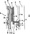
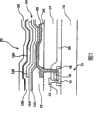
图1是第1实施例所涉及面板的一个像素的微腔部分构造的示意图。FIG. 1 is a schematic diagram of the microcavity structure of one pixel of the panel according to the first embodiment.
在玻璃基板10的预定部位形成有半导体层12,该半导体层12构成TFT、电极或配线。在图示之例中,半导体层12构成驱动TFT14的源极、沟道、漏极区域。该驱动TFT14的半导体层12由栅极氧化膜16所覆盖,而在该栅极氧化膜16上、即半导体层12的沟道区域上方形成有栅极电极18。全面形成层间绝缘膜20,并覆盖该闸极电极18与栅极氧化膜16。A
在驱动TFT14的源极区域,贯穿层间绝缘膜,连接源极电极22,形成平面化膜24并覆盖源极电极22及层间绝缘膜20。In the source region of the driving
在平面化膜24上形成有对应像素显示区域大小的透明电极26,该透明电极26通过连接孔连接在驱动TFT14的漏极区域。A
而且,该透明电极26的周边部由第2平面化膜28覆盖,在透明电极26上方配置有机EL元件30。Further, the peripheral portion of the
有机EL元件30是在透明电极26与正对电极32之间具备有机化合物,特别是具备至少包含有机发光材料的有机层(发光元件层)34的叠层构造,将空穴从阳极注入有机层34,将电子从阴极注入有机层34,在有机层中注入的空穴及电子会再次结合,利用所得的再结合能量激发有机发光材料,在回复到基底(基底)状态时产生发光。The
在此,透明电极26由例如ITO(氧化铟锡,indium tin oxide)或IZO(铟锌氧化物,indium zinc oxide)等导电性金属氧化物材料构成,正对电极32由起上部反射膜作用的Al或其合金制成。在透明电极26的下层局部设置有用以在透明电极26与上部反射膜(正对电极32)之间构成微小共振器(微腔)构造的下部反射膜36。也就是说,下部反射膜36并非设置在整个发光区域,而是设置在一部分上,未设置下部反射膜36的区域中来自有机层34的光会直接射向下方。Here, the
此例,涉及一种底发射(Bottom Emission)型显示装置,其使由有机层34所得的光从透明电极26穿透基板10并射出至外部,下部反射膜36可使一部分来自有机层34的光穿透、即具有半穿透性。该下部反射膜36可使用Ag、Au、Pt、Al的任一种或这些金属的合金膜,但可以是可穿透光的薄膜,也可以是网目状、格子状等具备开口部的图案。也可以是由交互叠层折射率不同的2种类以上的电介质的电介质多层膜构成。另外,各层电介质膜的光学膜厚优选的是,例如目的反射波长的1/4或其整数倍。This example relates to a bottom emission (Bottom Emission) type display device, which makes the light obtained by the
有机层34具备包含至少有机发光分子的发光层,依材料也有由单层、2层、3层或4层以上的多层叠层构造构成的情况。在图1的例子中,利用真空蒸镀法的连续成膜等,从作为起阳极作用的透明电极26侧,依次叠层空穴注入层122、空穴输送层124、发光层126、电子输送层128、电子注入层130,并利用与有机层34同样的真空蒸镀法,在电子注入层130上形成在此具有起阴极作用的正对电极32。并且,也可将电子注入层130作为对向电极32的一部分考虑。The
本实施例涉及的微腔构造形成在该透明电极26与正对电极32挟持着有机层34而正对着的区域,即透明电极26的下层的下部反射膜36与正对电极32所兼用的上部反射膜之间的层间。在此,该微腔的光学长度(光学距离)L以式(1)表示:L=∑nidi...,(1),即以形成在下部反射膜36与正对电极32(上部反射膜)的层间的各层厚度d、与该层的折射率n的积的和(i为叠层数且为不小于1的整数)表示。再者,该光学长度L相对于发光波长λ具有后式(3)所示的关系,按照所示关系进行设定,可以选择性增强波长λ并将其射出至外部。The microcavity structure involved in the present embodiment is formed in the area where the
在此,利用微腔构造增强特定的波长时,如上所述视角依存性会变高。因此,在本实施例中,在1个像素内具有不存在下部反射膜36的区域,在该区域中,来自有机层34的光直接射出。因此,来自不存在该下部反射膜36的区域的射出光并未因微腔构造而增强特定波长,而是具有较广范围的峰值的光,且视角依存性较小。因此,来自1像素的射出光可以增强特定波长,同时减低视角依存性。Here, when a specific wavelength is amplified by a microcavity structure, the viewing angle dependence becomes high as described above. Therefore, in this embodiment, there is a region in which the
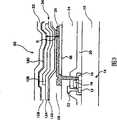
在此,全彩有机EL显示面板中,通常具有纯R、纯G、纯B的像素,相对于R、G、B的波长λ(λr、λg、λb),预定的光学长度L(Lr、Lg、Lb)由R、G、B的各像素决定。在此,下部反射膜36及正对电极32采用金属材料,在这些膜反射时的相位偏离在后式(3)中以
而且,在本实施例中,依据像素的发光色(按RGB分),变更存在有该下部反射膜36区域、未存在该下部反射膜36区域的面积比率。也就是说,如图2所示,存在有下部反射膜36区域的面积比率在R像素中最小,在G像素中为中等,在B像素中最大。In addition, in this embodiment, the area ratio of the area where the
再者,因视角所造成的共振波长变化,即波长越长视角依存性越大。图5说明共振波长与视角依存性的关系。横轴是在正面的共振波长,纵轴是视角60°时共振波长与正面共振波长的差。如图所示,视角依存性最高者为R。因此,如本实施例,存在有下部反射膜36区域的面积比率在R像素中最小,在G像素中为中等,在B像素中最大,而在RGB各色中,可同样地进行特定波长的增强及视角依存性的改善。Furthermore, the resonance wavelength changes due to the viewing angle, that is, the longer the wavelength, the greater the viewing angle dependence. Figure 5 illustrates the dependence of resonance wavelength on viewing angle. The horizontal axis is the resonance wavelength at the front, and the vertical axis is the difference between the resonance wavelength and the front resonance wavelength at a viewing angle of 60°. As shown in the figure, R is the one with the highest viewing angle dependence. Therefore, as in this embodiment, the area ratio of the region where the
在图2中,将存在有下部反射膜36的区域设为像素(发光区域)的中心部分,可以如图1所示配置在单侧,也可以形成若干个离散的区域等,可以在任意位置配置下部反射膜36。In FIG. 2, the region where the lower
第2实施例2nd embodiment
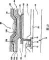
图3是第2实施例的构造图,下部反射膜36覆盖整个发光区域的。另一方面,有机层34在发光区域的一部分较厚。在本例中,空穴输送层124在发光区域、图中左区域较厚,在右区域较薄。FIG. 3 is a structural view of the second embodiment, in which the lower
微腔构造的特性由上部反射膜与下部反射膜36间的距离(微腔长度)来决定。因此,在本实施例中,在发光层2个区域中微腔的长度因有机层34的厚度而不同,由微腔构造所增强的光的波长因位置而不同。The characteristics of the microcavity structure are determined by the distance between the upper reflective film and the lower reflective film 36 (microcavity length). Therefore, in this embodiment, the length of the microcavity differs depending on the thickness of the
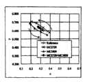
图4关于微腔的腔体长度D,在(1)2720埃(angstrom,以下称A)(MC=2720),(2)3800A(MC=3800),(3)无微腔(reference),(4)2720A及3800A(MC=2720+MC=3800,面积比为1∶1)时,表示各个发出绿光的有EL元件的视角依存性。而且,图4是CIE色品图(表色系)的色度图(色度図)(Y x y)。在此,微腔长度D是用于为了使预定波长的光共振而要求的上述光学长度L的反射膜与半穿透膜间的实际膜厚(膜厚合计),以D=∑di...(2)表示。Fig. 4 is about the cavity length D of microcavity, in (1) 2720 Angstrom (angstrom, hereinafter referred to as A) (MC=2720), (2) 3800A (MC=3800), (3) without microcavity (reference), (4) In the case of 2720A and 3800A (MC=2720+MC=3800, the area ratio is 1:1), it means that each EL element emitting green light has a viewing angle dependence. Furthermore, Fig. 4 is a chromaticity diagram (chromaticity map) (Y x y) of the CIE chromaticity diagram (color system). Here, the microcavity length D is the actual film thickness (total film thickness) between the reflective film and the semi-transmissive film of the above-mentioned optical length L required to resonate light of a predetermined wavelength, and D=Σdi.. .(2) means.
MC=2720以图中x表示,在视角0°时具有570nm的共振波长,为右下(x=0.39,Y=0.58)所示的色度,随着视角变大共振波长会向短波长侧位移(朝图中的左上方移动)。在视角60°时,具有520nm的共振波长,可获得色纯度高的绿色,如图中左上(x=0.21,y=0.71)所示。MC=2720 is represented by x in the figure. It has a resonance wavelength of 570nm at a viewing angle of 0°, which is the chromaticity shown in the lower right (x=0.39, Y=0.58). As the viewing angle becomes larger, the resonance wavelength will shift to the shorter wavelength side Displacement (towards the upper left in the figure). When the viewing angle is 60°, it has a resonance wavelength of 520nm, and can obtain green with high color purity, as shown in the upper left of the figure (x=0.21, y=0.71).
另一方面,MC=3800以黑三角表示,在视角0°(即相对于微腔为正面)时具有510nm的共振波长,为图中左上(x=0.19,Y=0.69)的色纯度高的绿色,随着视角变大,共振波长会向短波长侧位移,即朝图中右下方移动,在视角60°时,到达图中右下(x=0.37,y=0.55)的位置。再者,起因于使用在该元件上的有机发光材料的发光光谱,由于在绿色时具有峰值,且蓝色成分较少,所以即使共振波长随着视角变大而位移,原来的发光光谱中的该共振波长成分较小,因此元件的发光强度会降低,成为绿色的半穿透光。无微腔(Reference)以◇表示,其移动范围为x=0.30至0.33,y=0.60至0.63左右,视角依存性相对较小。而且,在本实施例中MC=2720+MC=3800,其视角依存性比单一微腔条件时更小。也就是,在视角为0°、MC3800A时,在视角为60°、MC2700A时可以呈现出高的色纯度,因此不论在哪一个视角,都可以经常维持高的色纯度。因此,在组合若干个微腔长度不同的区域的元件中,色度的移动范围是在x=0.27至0.29,y=0.63至0.65左右,在色度图上相比无微腔更位于左上方,并且位移较少,色纯度会提升。On the other hand, MC=3800 is represented by a black triangle, and has a resonance wavelength of 510nm at a viewing angle of 0° (that is, facing the front of the microcavity), which is the color purity of the upper left (x=0.19, Y=0.69) in the figure. Green, as the viewing angle becomes larger, the resonance wavelength will shift to the short wavelength side, that is, move to the lower right in the figure, and reach the lower right position in the figure (x=0.37, y=0.55) when the viewing angle is 60°. Furthermore, since the emission spectrum of the organic light-emitting material used in this device has a peak in green and less blue components, even if the resonance wavelength shifts as the viewing angle becomes larger, the original emission spectrum This resonant wavelength component is small, so the luminous intensity of the device is reduced, and it becomes green semi-transmissive light. No microcavity (Reference) is represented by ◇, its moving range is about x=0.30 to 0.33, y=0.60 to 0.63, and the viewing angle dependence is relatively small. Moreover, in this embodiment, MC=2720+MC=3800, the viewing angle dependence is smaller than that of a single microcavity. That is, when the viewing angle is 0°, MC3800A can show high color purity when the viewing angle is 60°, MC2700A, so regardless of the viewing angle, high color purity can always be maintained. Therefore, in an element combining several regions with different lengths of microcavities, the moving range of the chromaticity is around x=0.27 to 0.29, y=0.63 to 0.65, and it is located in the upper left of the chromaticity diagram than that without microcavities , and the displacement is less, the color purity will be improved.
如此,根据本实施例的结构,在1像素内分别构成2720A、3800A的2种厚度(1100A左右的等级差别)的微腔,因而大幅改善(减少)针对绿色的光的视角依存性。Thus, according to the structure of the present embodiment, microcavities of two types of thicknesses of 2720A and 3800A (level difference of about 1100A) are formed in one pixel, thereby greatly improving (reducing) the viewing angle dependence of green light.
在此,共振条件与共振波长的视角依存性由下式表示。Here, the viewing angle dependence of the resonance condition and the resonance wavelength is represented by the following equation.
[数1][number 1]
θ’=sinθ-1{(sinθ)/n}θ'=sinθ-1 {(sinθ)/n}
λ’=λ+(cosθ-1)λλ'=λ+(cosθ-1)λ
再者,在式中的L代表上述光学长度D(D=∑nidi...),
图5表示在横轴为视角0°时峰值波长,纵轴为视角60°时峰值波长朝短波长侧位移的位移量。微腔长度D设为4500A至5500A。如此,在视角0°时峰值波长为450nm左右,视角60°时波长的位移量在28nm左右。而且,在视角0°、峰值波长450nm左右的条件下,视角60°时波长的位移量在60nm左右。5 shows the peak wavelength at a viewing angle of 0° on the horizontal axis and the shift amount of the peak wavelength toward the shorter wavelength side at a viewing angle of 60° on the vertical axis. The microcavity length D is set at 4500A to 5500A. In this way, the peak wavelength is about 450 nm when the viewing angle is 0°, and the wavelength shift amount is about 28 nm when the viewing angle is 60°. Moreover, under the conditions of a viewing angle of 0° and a peak wavelength of about 450 nm, the wavelength shift is about 60 nm when the viewing angle is 60°.
如此,在视角0°且峰值波长为600nm的波形在视角60°的方向上观察,其峰值波长向短方向位移60nm成为峰值波长为540nm的波形。因此,为了在绿光550nm的情况下进行内插,与600nm至700nm左右的微腔长度D(共振波长在600nm至700nm的微腔长度D)加以组合。由上式可知,在m=1时,等级差别大致为1000A(100nm)至1300A(130nm)。Thus, when a waveform with a peak wavelength of 600 nm at a viewing angle of 0° is viewed from a viewing angle of 60°, its peak wavelength shifts 60 nm in the shorter direction to a waveform with a peak wavelength of 540 nm. Therefore, in order to perform interpolation in the case of green light of 550 nm, it is combined with a microcavity length D of about 600 nm to 700 nm (microcavity length D at a resonance wavelength of 600 nm to 700 nm). It can be seen from the above formula that when m=1, the level difference is approximately 1000A (100nm) to 1300A (130nm).
再者,MC=2720及MC=3800分别相对于视角0°的光的共振波长为570nm(m=1)、510nm(m=2)。也就是说,在上述例中,视角依存性较小,为作成对绿光的微腔,在视角为0°时,在1个像素内组合将510nm、570nm作为共振峰值的微腔长度D。In addition, the resonance wavelengths of MC=2720 and MC=3800 are 570 nm (m=1) and 510 nm (m=2) respectively with respect to light with a viewing angle of 0°. That is to say, in the above example, the viewing angle dependence is small, and in order to form a microcavity for green light, when the viewing angle is 0°, the microcavity length D with 510nm and 570nm as resonance peaks is combined in one pixel.
而且,对红光630nm,优选的是,组合700nm至800nm左右的微腔长度D,在m=1时,等级差别大致为1600A左右。对蓝光450nm,优选的是,组合480nm至580nm左右的微腔长度D,在m=1时,等级差别大致为1000A左右。Moreover, for the red light of 630nm, it is preferable to combine the microcavity length D of about 700nm to 800nm, and when m=1, the level difference is about 1600A. For the blue light of 450nm, it is preferable to combine the microcavity length D of about 480nm to 580nm, and when m=1, the level difference is about 1000A.
再者,等级差别因m选值不同而不同,但考虑等级差别被覆性(被覆性)时,优选的是,将等级差别控制在2000A以下。也就是在将1个像素中的微腔长度互不相同的区域定义为第1区域(例如上述MC3800A)与第2区域(例如上述MC2700A)时,第1区域的微腔长度D与第2区域的微腔长度D,优选的是,考虑其分别与目的共振波长、原来的发光光谱、彩色滤光片组合时的滤光特性等,分别确定,优选的是,将微腔长度的差(等级差别)控制在200nm(2000A)以内。由于设定在上述范围内,如上所述即使在变更透明电极的厚度而形成第1及第2区域时,凭借形成在透明电极上的等级差别,可以防止电极上层的断线等。例如,电子输送层的厚度变厚时,可能导致驱动电压上升,由于并不希望电压上升,因此大多设定为未满3000A的厚度,从该电子输送层因利用等级差别防止断线的观点来看,优选的是,将等级差别控制在200nm以下。Furthermore, the grade difference varies depending on the selected value of m, but in consideration of the grade difference coverage (coverability), it is preferable to control the grade difference below 2000A. That is, when the regions in which the microcavity lengths in one pixel are different from each other are defined as the first region (such as the above-mentioned MC3800A) and the second region (such as the above-mentioned MC2700A), the microcavity length D of the first region and the second region The length D of the microcavity, it is preferable to consider its filter characteristics etc. when it is combined with the target resonant wavelength, the original luminescence spectrum and the color filter respectively, and determine respectively, preferably, the difference of the length of the microcavity (grade difference) is controlled within 200nm (2000A). By setting it within the above range, even when the first and second regions are formed by changing the thickness of the transparent electrode as described above, it is possible to prevent disconnection of the upper layer of the electrode due to the level difference formed on the transparent electrode. For example, when the thickness of the electron transport layer becomes thicker, the driving voltage may increase. Since the voltage increase is not desired, the thickness is often set to less than 3000 A. From the viewpoint of preventing disconnection due to the use of level differences in the electron transport layer See, it is preferable to control the level difference below 200nm.
如上所述,可知在某颜色的1个像素区域中,因设定若干个微腔长度D,可改善视角依存性并使色纯度提升,但在此所选择的若干个微腔长度D,例如在第1区域的1个微腔长度D在视角0°时设定为原本目的的共振波长为峰值波长的厚度,在第2区域的与第1区域不同的用于补偿微腔长度D在其它视角(例如60°)时,设定为目的的共振波长为峰值波长的厚度。再者,所选择的若干个微腔长度D都比较长也可以。在以上的说明中,在1个像素内形成2种微腔长度不同的区域,但是并不限于2种,也可以依需要形成3种或3种以上。As mentioned above, it can be seen that in one pixel area of a certain color, by setting several microcavity lengths D, the viewing angle dependence can be improved and the color purity can be improved. However, the several microcavity lengths D selected here, such as The length D of one microcavity in the first region is set as the thickness of the original resonance wavelength as the peak wavelength when the viewing angle is 0°, and the length D of the microcavity in the second region is different from the first region to compensate the length D of the microcavity in the other When the viewing angle (for example, 60°), set the target resonance wavelength as the thickness of the peak wavelength. Furthermore, the lengths D of the selected microcavities are relatively long. In the above description, two types of regions with different lengths of microcavities are formed in one pixel, but they are not limited to two types, and three or more types may be formed as required.
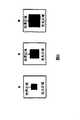
而且,在本实施例中,用于补偿的微腔的有机层的厚度较薄时,依据像素的发光颜色(RGB的差别),变更有机层34厚度较厚的区域、与用于补偿的微腔厚度较薄区域的面积比率。即,如图6所示之模式,有机层34较厚区域的面积比率在R像素中最小,在G像素中为中等,而在B像素中为最大。Moreover, in this embodiment, when the thickness of the organic layer of the microcavity used for compensation is relatively thin, according to the luminous color (the difference of RGB) of the pixel, the thicker region of the
这是由于如上所述调查微腔构造特定波长的视角(因视角而产生变化)特性时,波长越长其视角依存性越高的缘故。This is because, when the viewing angle (variation due to viewing angle) characteristic of a specific wavelength of a microcavity structure is investigated as described above, the longer the wavelength, the higher the viewing angle dependence.
这样,根据有机层34较厚区域的面积比率在R像素中最小,在G像素中为中等,在B像素中为最大,而在RGB各色中,同样进行特定波长的增强及视角依存性的改善。In this way, according to the area ratio of the thicker region of the
而且,不但可适当变更有机层34的厚度,也可变更透明电极26的厚度。Furthermore, not only the thickness of the
第3实施例3rd embodiment
图7是第3实施例的构造图。下部反射膜36覆盖整个发光区域。而且,该下部反射膜36由上述电介质多层膜构成,并且使其厚度在1个像素(1个发光区域)内不同。即,在厚度较厚的区域中,电介质叠层数会变大。在该例中,下部反射膜36的厚度在发光区域图中的左区域较厚,在右区域较薄。Fig. 7 is a structural diagram of the third embodiment. The lower
微腔构造由上部反射膜与下部反射膜36间的距离(微腔长度)来决定特性。因此,在本实施例中,变更下部反射膜36的厚度时,其厚度越厚,微腔构造的特定波长的光的增强效果也越大。因此,在本实施例中,在1个像素中,形成对于特定波长的光的增强效果较大的区域及对于特定波长的光的增强效果较小的区域。由此,可增强特定波长的光,同时可降低视角依存性。The characteristics of the microcavity structure are determined by the distance between the upper reflective film and the lower reflective film 36 (microcavity length). Therefore, in this embodiment, when the thickness of the
而且,在本实施例中,与上述实施例同样依据像素的发光颜色(RGB的差别),变更该下部反射膜36厚度较厚的区域、与该下部反射膜36厚度较薄的区域的面积比率。即,如图7所示之模式,下部反射膜36较厚区域的面积比率在R像素中最小,在G像素中为中等,在B像素中为最大。In addition, in this embodiment, the ratio of the area of the thicker region of the
由此,在RGB各色中,同样进行特定波长的增强及视角依存性的改善。Accordingly, enhancement of specific wavelengths and improvement of viewing angle dependence are similarly performed for each color of RGB.
其它实施例other embodiments
图8至图10表示其它实施例,且为使光朝与玻璃基板10相反方向射出的顶射极型(top emission)。因此,配置在起阳极作用的透明电极26与平面化膜24之间的下部反射膜36并非半穿透膜,而是反射膜。因此,来自有机层34的光并未穿透玻璃基板10。8 to 10 show other embodiments, and are of a top emission type in which light is emitted in a direction opposite to the
另一方面,正对电极32由ITO或IZO等透明导电膜制成,在该正对电极上设置半穿透膜40。因此,在下部反射膜36与半穿透膜40之间形成有微腔构造。On the other hand, the
在图8中,在正对电极32上的发光区域局部设置有半穿透膜40。因此设置有半穿透膜40的部分,形成有微腔构造且使特定波长的光增强,而在未存在半穿透膜40的区域,光直接射出至上方。因此,与图1的情形相同,可一面增强特定波长的光,一面改善视角依存性。In FIG. 8 , a
在图9中,在整个正对电极32上设置半穿透膜40,但与图3的情形相同,空穴输送层124厚度不均匀。因此,光的射出方向不同,但仍然可以获得与图3所示构造同样的效果。而且,微腔长度不同,可以变更有机层34中任一层或若干层的厚度,也可以变更透明电极26或正对电极32的厚度。In FIG. 9 , the
在图10中,在整个正对电极32上设置半穿透膜40,但与图8的情形相同,半穿透膜40的厚度不均匀。因此,光的射出方向不同,但仍然可以获得与图7所示构造同样的效果。In FIG. 10 , the
而且,在该图8至图10的例子,通过在RGB各色中变更(1)设置有半穿透膜40的区域与未设置半穿透膜40的区域的面积比率、(2)有机层34等厚度不同的区域的面积比率、(3)半穿透膜的厚度较厚区域与半穿透膜的厚度较薄区域的面积比率,可以减小各色微腔的影响差,并可以达到有效改善视角依存性的目的。该面积比率的变更方式与图2及图6所示相同,可以任意选择其位置、大小、个数等。8 to 10, by changing (1) the area ratio of the area where the
Claims (5)
Translated fromChineseApplications Claiming Priority (2)
| Application Number | Priority Date | Filing Date | Title |
|---|---|---|---|
| JP2005053894 | 2005-02-28 | ||
| JP2005053894AJP4573672B2 (en) | 2005-02-28 | 2005-02-28 | Organic EL panel |
Publications (2)
| Publication Number | Publication Date |
|---|---|
| CN1832195A CN1832195A (en) | 2006-09-13 |
| CN100438068Ctrue CN100438068C (en) | 2008-11-26 |
Family
ID=36931275
Family Applications (1)
| Application Number | Title | Priority Date | Filing Date |
|---|---|---|---|
| CNB2006100580430AActiveCN100438068C (en) | 2005-02-28 | 2006-02-28 | Organic el panel |
Country Status (5)
| Country | Link |
|---|---|
| US (2) | US8129712B2 (en) |
| JP (1) | JP4573672B2 (en) |
| KR (1) | KR20060095494A (en) |
| CN (1) | CN100438068C (en) |
| TW (1) | TW200631466A (en) |
Families Citing this family (47)
| Publication number | Priority date | Publication date | Assignee | Title |
|---|---|---|---|---|
| US8339037B2 (en)* | 2004-03-26 | 2012-12-25 | Panasonic Corporation | Organic light emitting device with reduced angle dependency |
| JP4411288B2 (en) | 2005-03-23 | 2010-02-10 | キヤノン株式会社 | Display device |
| TWI358964B (en)* | 2006-04-12 | 2012-02-21 | Au Optronics Corp | Electroluminescence display element and method for |
| KR100942365B1 (en)* | 2007-02-05 | 2010-02-12 | 주식회사 엘지화학 | Organic light emitting device having excellent luminous efficiency and manufacturing method thereof |
| TWI363441B (en)* | 2007-02-09 | 2012-05-01 | Au Optronics Corp | Self-emissive display device |
| CN101017884B (en)* | 2007-02-28 | 2013-08-14 | 友达光电股份有限公司 | Self-lighting display device |
| JP5167723B2 (en) | 2007-08-21 | 2013-03-21 | セイコーエプソン株式会社 | Light emitting device |
| US7855508B2 (en)* | 2007-09-17 | 2010-12-21 | Global Oled Technology Llc | LED device having improved light output |
| US7741770B2 (en) | 2007-10-05 | 2010-06-22 | Global Oled Technology Llc | LED device having improved light output |
| TWI367684B (en)* | 2007-11-02 | 2012-07-01 | Chimei Innolux Corp | Organic light emitting display device and electronic device |
| KR101404546B1 (en) | 2007-11-05 | 2014-06-09 | 삼성디스플레이 주식회사 | Organic light emitting display and manufacturing method thereof |
| KR20090083197A (en) | 2008-01-29 | 2009-08-03 | 삼성전자주식회사 | Method of manufacturing color filter substrate |
| JP2009231274A (en)* | 2008-02-27 | 2009-10-08 | Canon Inc | Organic light-emitting element, and display apparatus |
| US7893612B2 (en)* | 2008-02-27 | 2011-02-22 | Global Oled Technology Llc | LED device having improved light output |
| JP5315761B2 (en)* | 2008-04-15 | 2013-10-16 | セイコーエプソン株式会社 | Organic electroluminescence device |
| KR100909389B1 (en) | 2008-04-21 | 2009-07-24 | 삼성모바일디스플레이주식회사 | Organic light emitting display device |
| JP2009289592A (en)* | 2008-05-29 | 2009-12-10 | Canon Inc | Display |
| KR101603314B1 (en) | 2008-09-11 | 2016-03-15 | 삼성디스플레이 주식회사 | Organic light emitting diode display and method for manufacturing the same |
| KR20100059447A (en) | 2008-11-26 | 2010-06-04 | 삼성전자주식회사 | Organic light emitting diode display |
| KR101582941B1 (en) | 2008-12-24 | 2016-01-08 | 삼성디스플레이 주식회사 | Organic light emitting device and manufacturing method thereof |
| US8183561B2 (en)* | 2009-06-24 | 2012-05-22 | Au Optronics Corporation | OLED panel with broadened color spectral components |
| KR101232736B1 (en)* | 2009-10-01 | 2013-02-13 | 엘지디스플레이 주식회사 | Array substrate for organic electroluminescent device |
| KR101084240B1 (en) | 2009-12-21 | 2011-11-16 | 삼성모바일디스플레이주식회사 | Organic light emitting diode display |
| JP2014078536A (en)* | 2010-03-15 | 2014-05-01 | Pioneer Electronic Corp | Organic el device |
| KR20120042066A (en)* | 2010-10-22 | 2012-05-03 | 삼성모바일디스플레이주식회사 | Organic light emitting diode display |
| KR101970675B1 (en)* | 2011-08-04 | 2019-04-19 | 가부시키가이샤 한도오따이 에네루기 켄큐쇼 | Light-emitting device and lighting device |
| JP5963458B2 (en)* | 2012-01-31 | 2016-08-03 | キヤノン株式会社 | LIGHT EMITTING DEVICE, IMAGE FORMING DEVICE, AND IMAGING DEVICE |
| JP2013165014A (en)* | 2012-02-13 | 2013-08-22 | Seiko Epson Corp | Organic el device and electronic apparatus |
| TWI588540B (en)* | 2012-05-09 | 2017-06-21 | 半導體能源研究所股份有限公司 | Display device and electronic device |
| TWI611215B (en)* | 2012-05-09 | 2018-01-11 | 半導體能源研究所股份有限公司 | Display device and electronic device |
| CN103811669B (en)* | 2012-11-09 | 2016-08-17 | 上海天马微电子有限公司 | Organic light emitting device, organic light emitting diode display apparatus and method of manufacturing the same |
| KR102098068B1 (en)* | 2013-08-13 | 2020-04-07 | 엘지디스플레이 주식회사 | White organic light emitting diode display device using micro cavity |
| KR20150061558A (en)* | 2013-11-26 | 2015-06-04 | 엘지디스플레이 주식회사 | Organic light emitting display device |
| US9627649B2 (en)* | 2013-11-26 | 2017-04-18 | Lg Display Co., Ltd. | Organic light emitting display device |
| JP2015201314A (en)* | 2014-04-07 | 2015-11-12 | 株式会社ジャパンディスプレイ | Light emitting element display device |
| CN104900684B (en) | 2015-06-12 | 2018-01-30 | 京东方科技集团股份有限公司 | Display base plate and preparation method thereof, display device |
| KR102181121B1 (en) | 2016-09-20 | 2020-11-20 | 주식회사 원익아이피에스 | Substrate transfer apparatus and control method of substrate transfer apparatus |
| KR102439873B1 (en)* | 2017-03-10 | 2022-09-05 | 삼성디스플레이 주식회사 | Organic light-emitting apparatus and the method for manufacturing of the organic light-emitting display apparatus |
| JP2019079699A (en)* | 2017-10-25 | 2019-05-23 | 株式会社ジャパンディスプレイ | Display device |
| KR102632542B1 (en)* | 2018-07-30 | 2024-01-31 | 엘지디스플레이 주식회사 | Organic light emitting display apparatus |
| KR102662750B1 (en)* | 2018-12-20 | 2024-04-30 | 엘지디스플레이 주식회사 | Display device |
| CN109950298A (en)* | 2019-04-17 | 2019-06-28 | 京东方科技集团股份有限公司 | A display substrate, its preparation method, and display device |
| JP7689419B2 (en)* | 2019-10-28 | 2025-06-06 | キヤノン株式会社 | Organic device, its manufacturing method, display device, photoelectric conversion device, electronic device, lighting device, and mobile object |
| CN113594386B (en)* | 2021-07-28 | 2022-09-23 | 京东方科技集团股份有限公司 | Display panel and display device |
| JP7644743B2 (en)* | 2021-12-13 | 2025-03-12 | キヤノン株式会社 | Light-emitting device, display device, imaging device and electronic device |
| WO2025088750A1 (en)* | 2023-10-26 | 2025-05-01 | シャープディスプレイテクノロジー株式会社 | Light-emitting element, display device, and method for manufacturing light-emitting element |
| US20250295011A1 (en)* | 2023-11-17 | 2025-09-18 | Beijing Boe Technology Development Co., Ltd. | Display panel and display device |
Citations (4)
| Publication number | Priority date | Publication date | Assignee | Title |
|---|---|---|---|---|
| US6111270A (en)* | 1998-04-27 | 2000-08-29 | Motorola, Inc. | Light-emitting apparatus and method of fabrication |
| CN1543281A (en)* | 2003-02-18 | 2004-11-03 | ��˹���´﹫˾ | Tuned microcavity color OLED displays |
| US20040217700A1 (en)* | 2003-04-28 | 2004-11-04 | Shu-Wen Chang | Full color organic electro-luminescence display panel with adjustable color purity and method of manufacturing the same |
| US20050040756A1 (en)* | 2003-08-19 | 2005-02-24 | Eastman Kodak Company | OLED device having microcavity gamut subpixels and a within gamut subpixel |
Family Cites Families (31)
| Publication number | Priority date | Publication date | Assignee | Title |
|---|---|---|---|---|
| JP2797883B2 (en)* | 1993-03-18 | 1998-09-17 | 株式会社日立製作所 | Multicolor light emitting device and its substrate |
| US5405710A (en) | 1993-11-22 | 1995-04-11 | At&T Corp. | Article comprising microcavity light sources |
| JP3420399B2 (en)* | 1995-07-28 | 2003-06-23 | キヤノン株式会社 | Light emitting element |
| US5686360A (en) | 1995-11-30 | 1997-11-11 | Motorola | Passivation of organic devices |
| JP4001692B2 (en) | 1999-02-18 | 2007-10-31 | パイオニア株式会社 | Organic electroluminescence device and manufacturing method thereof |
| GB2351840A (en) | 1999-06-02 | 2001-01-10 | Seiko Epson Corp | Multicolour light emitting devices. |
| GB2353400B (en) | 1999-08-20 | 2004-01-14 | Cambridge Display Tech Ltd | Mutiple-wavelength light emitting device and electronic apparatus |
| TW522453B (en) | 1999-09-17 | 2003-03-01 | Semiconductor Energy Lab | Display device |
| TW466889B (en) | 1999-11-22 | 2001-12-01 | Sony Corp | Display device |
| US6710541B2 (en) | 2000-12-22 | 2004-03-23 | Reveo, Inc. | Polarized light sources and methods for making the same |
| US6576351B2 (en) | 2001-02-16 | 2003-06-10 | Universal Display Corporation | Barrier region for optoelectronic devices |
| JP2003109775A (en) | 2001-09-28 | 2003-04-11 | Sony Corp | Organic electroluminescent device |
| KR100490535B1 (en) | 2001-12-17 | 2005-05-17 | 삼성에스디아이 주식회사 | Organic electroluminescence device |
| JP3748406B2 (en) | 2001-12-18 | 2006-02-22 | 株式会社日立製作所 | Display device |
| KR100834342B1 (en) | 2001-12-29 | 2008-06-02 | 엘지디스플레이 주식회사 | Active matrix organic electroluminescent device and manufacturing method thereof |
| KR20030069707A (en) | 2002-02-22 | 2003-08-27 | 엘지.필립스 엘시디 주식회사 | Organic Electroluminescent Device and Method for Fabricating the same |
| US6670772B1 (en) | 2002-06-27 | 2003-12-30 | Eastman Kodak Company | Organic light emitting diode display with surface plasmon outcoupling |
| US6747618B2 (en)* | 2002-08-20 | 2004-06-08 | Eastman Kodak Company | Color organic light emitting diode display with improved lifetime |
| JP4208526B2 (en) | 2002-09-12 | 2009-01-14 | キヤノン株式会社 | ORGANIC EL DISPLAY DEVICE AND ELECTRONIC DEVICE HAVING THE DISPLAY DEVICE |
| US6737800B1 (en) | 2003-02-18 | 2004-05-18 | Eastman Kodak Company | White-emitting organic electroluminescent device with color filters and reflective layer for causing colored light constructive interference |
| US6812637B2 (en) | 2003-03-13 | 2004-11-02 | Eastman Kodak Company | OLED display with auxiliary electrode |
| JP4895490B2 (en) | 2003-09-30 | 2012-03-14 | 三洋電機株式会社 | Organic EL panel |
| JP4497881B2 (en) | 2003-09-30 | 2010-07-07 | 三洋電機株式会社 | Organic EL device and organic EL panel |
| JP4428979B2 (en) | 2003-09-30 | 2010-03-10 | 三洋電機株式会社 | Organic EL panel |
| US7268485B2 (en) | 2003-10-07 | 2007-09-11 | Eastman Kodak Company | White-emitting microcavity OLED device |
| JP2005302313A (en) | 2004-04-06 | 2005-10-27 | Idemitsu Kosan Co Ltd | Organic EL display device and full color device |
| JPWO2005107327A1 (en) | 2004-04-30 | 2008-03-21 | 三洋電機株式会社 | Luminous display |
| JP2005322435A (en)* | 2004-05-06 | 2005-11-17 | Seiko Epson Corp | Electroluminescent element and display element |
| US7023013B2 (en)* | 2004-06-16 | 2006-04-04 | Eastman Kodak Company | Array of light-emitting OLED microcavity pixels |
| TWI272039B (en) | 2004-06-18 | 2007-01-21 | Sanyo Electric Co | Electroluminescence panel |
| JP4731211B2 (en)* | 2004-06-18 | 2011-07-20 | 三洋電機株式会社 | Electroluminescence panel |
- 2005
- 2005-02-28JPJP2005053894Apatent/JP4573672B2/ennot_activeExpired - Lifetime
- 2006
- 2006-01-27TWTW095103420Apatent/TW200631466A/enunknown
- 2006-02-27USUS11/362,965patent/US8129712B2/enactiveActive
- 2006-02-27KRKR1020060018656Apatent/KR20060095494A/ennot_activeCeased
- 2006-02-28CNCNB2006100580430Apatent/CN100438068C/enactiveActive
- 2012
- 2012-01-20USUS13/354,472patent/US20120112234A1/ennot_activeAbandoned
Patent Citations (4)
| Publication number | Priority date | Publication date | Assignee | Title |
|---|---|---|---|---|
| US6111270A (en)* | 1998-04-27 | 2000-08-29 | Motorola, Inc. | Light-emitting apparatus and method of fabrication |
| CN1543281A (en)* | 2003-02-18 | 2004-11-03 | ��˹���´﹫˾ | Tuned microcavity color OLED displays |
| US20040217700A1 (en)* | 2003-04-28 | 2004-11-04 | Shu-Wen Chang | Full color organic electro-luminescence display panel with adjustable color purity and method of manufacturing the same |
| US20050040756A1 (en)* | 2003-08-19 | 2005-02-24 | Eastman Kodak Company | OLED device having microcavity gamut subpixels and a within gamut subpixel |
Also Published As
| Publication number | Publication date |
|---|---|
| JP4573672B2 (en) | 2010-11-04 |
| KR20060095494A (en) | 2006-08-31 |
| TW200631466A (en) | 2006-09-01 |
| US20120112234A1 (en) | 2012-05-10 |
| US20060192220A1 (en) | 2006-08-31 |
| US8129712B2 (en) | 2012-03-06 |
| JP2006236947A (en) | 2006-09-07 |
| CN1832195A (en) | 2006-09-13 |
| TWI336212B (en) | 2011-01-11 |
Similar Documents
| Publication | Publication Date | Title |
|---|---|---|
| CN100438068C (en) | Organic el panel | |
| CN100459213C (en) | Electroluminescence panel | |
| JP4731211B2 (en) | Electroluminescence panel | |
| KR101056679B1 (en) | Organic light emitting device and display device | |
| KR101354303B1 (en) | Display unit | |
| US7973469B2 (en) | Organic electroluminescence element, and illuminating device and display device therewith | |
| US7586257B2 (en) | Organic el panel with organic layer for emitting light of a specific color and organic layer for emitting white light | |
| KR101990312B1 (en) | Organic Light Emitting Diode Display Device and Method for Manufacturing The Same | |
| JP2009049223A (en) | Light emitting device | |
| US8421345B2 (en) | Electroluminescent device including white color filter pattern having blue light transmittance greater than red and green light transmittance | |
| CN106373978B (en) | Thin film transistor array substrate and organic light emitting diode display device including same | |
| US20050088084A1 (en) | Organic polarized light emitting diode display with polarizer | |
| KR20100071539A (en) | Organic light emitting device and method for manufacturing the same | |
| US20110215302A1 (en) | Organic light emitting diode (oled) display | |
| CN112310307A (en) | OLED display panel | |
| KR102618926B1 (en) | Organic light emitting diode display device | |
| KR101622913B1 (en) | Organic Light Emitting Display Device and fabricating of the same | |
| JP2006278257A (en) | Organic light emitting device and its manufacturing method | |
| JP2006278258A (en) | Organic light-emitting device | |
| KR102572434B1 (en) | Organic light emitting diodes display | |
| CN101350361A (en) | EL device and electronic equipment | |
| JP4911652B2 (en) | Organic EL panel | |
| KR102562975B1 (en) | Light emitting diode and Electroluminescent display device including the same | |
| GB2439356A (en) | Organic electroluminescent devices |
Legal Events
| Date | Code | Title | Description |
|---|---|---|---|
| C06 | Publication | ||
| PB01 | Publication | ||
| C10 | Entry into substantive examination | ||
| SE01 | Entry into force of request for substantive examination | ||
| C14 | Grant of patent or utility model | ||
| GR01 | Patent grant |