CN100433056C - Signal processing circuit and non-contrct ic card using same and tag - Google Patents
Signal processing circuit and non-contrct ic card using same and tagDownload PDFInfo
- Publication number
- CN100433056C CN100433056CCNB2006100772498ACN200610077249ACN100433056CCN 100433056 CCN100433056 CCN 100433056CCN B2006100772498 ACNB2006100772498 ACN B2006100772498ACN 200610077249 ACN200610077249 ACN 200610077249ACN 100433056 CCN100433056 CCN 100433056C
- Authority
- CN
- China
- Prior art keywords
- mentioned
- strip conductor
- conductor circuit
- frequency
- circuit
- Prior art date
- Legal status (The legal status is an assumption and is not a legal conclusion. Google has not performed a legal analysis and makes no representation as to the accuracy of the status listed.)
- Expired - Fee Related
Links
Images


Classifications
- H—ELECTRICITY
- H01—ELECTRIC ELEMENTS
- H01Q—ANTENNAS, i.e. RADIO AERIALS
- H01Q9/00—Electrically-short antennas having dimensions not more than twice the operating wavelength and consisting of conductive active radiating elements
- H01Q9/04—Resonant antennas
- H01Q9/16—Resonant antennas with feed intermediate between the extremities of the antenna, e.g. centre-fed dipole
- H01Q9/28—Conical, cylindrical, cage, strip, gauze, or like elements having an extended radiating surface; Elements comprising two conical surfaces having collinear axes and adjacent apices and fed by two-conductor transmission lines
- H01Q9/285—Planar dipole
- H—ELECTRICITY
- H01—ELECTRIC ELEMENTS
- H01Q—ANTENNAS, i.e. RADIO AERIALS
- H01Q1/00—Details of, or arrangements associated with, antennas
- H01Q1/12—Supports; Mounting means
- H01Q1/22—Supports; Mounting means by structural association with other equipment or articles
- H—ELECTRICITY
- H01—ELECTRIC ELEMENTS
- H01Q—ANTENNAS, i.e. RADIO AERIALS
- H01Q9/00—Electrically-short antennas having dimensions not more than twice the operating wavelength and consisting of conductive active radiating elements
- H01Q9/04—Resonant antennas
- H01Q9/16—Resonant antennas with feed intermediate between the extremities of the antenna, e.g. centre-fed dipole
- H01Q9/26—Resonant antennas with feed intermediate between the extremities of the antenna, e.g. centre-fed dipole with folded element or elements, the folded parts being spaced apart a small fraction of operating wavelength
- H01Q9/27—Spiral antennas
Landscapes
- Near-Field Transmission Systems (AREA)
- Details Of Aerials (AREA)
- Credit Cards Or The Like (AREA)
Abstract
Translated fromChineseDescription
Translated fromChinese技术领域technical field
本发明涉及例如在现金自动支付机、电子货币、自动检票系统、出入室管理系统、商品管理系统、物流管理系统等中的闪存卡、信用卡、月票、回数券、管理卡、ID卡、许可证、商品管理标签、物流管理标签等非接触卡或者标签中所设置的信号处理电路,涉及具备在该非接触卡或者标签与读写器的动作用电力传输或者通信中使用的天线的信号处理电路。The present invention relates to flash memory cards, credit cards, commuter passes, coupons, management cards, ID cards, licenses, etc. A signal processing circuit provided in a contactless card or label such as a commodity management label or a logistics management label, relating to a signal processing circuit provided with an antenna used for power transmission or communication between the contactless card or label and a reader/writer .
背景技术Background technique
在非接触IC卡或者标签中,主要使用HF(高频)频带到UHF(超高频)频带的频率的电磁波进行电力传输和通信。一般HF频带作为3~30MHz的频带是已知的,特别是由13.56MHz的载波进行的非接触卡或者标签(以下,把它们汇总在一起,记为RFID(射频标识))与读写器的通信或者电力传输正在普及。UHF频带作为300~3000MHz的频带一般是已知的,在日本国内,2.45GHz的频带,在欧美860~960MHz的频带能够利用在RFID与读写器的通信或者电力传输中。另外,作为比上述频带高的频率的5.8GHz在日本国内,允许利用为收费公路中的仅从RFID向读出器的单向通信用频率。In a non-contact IC card or tag, electric power transmission and communication are mainly performed using electromagnetic waves at frequencies from HF (High Frequency) band to UHF (Ultra High Frequency) band. Generally, the HF frequency band is known as a frequency band of 3 to 30 MHz. In particular, contactless cards or tags performed by a carrier wave of 13.56 MHz (hereafter, they are collectively referred to as RFID (Radio Frequency Identification)) and readers. Communication or power transmission is gaining popularity. The UHF frequency band is generally known as a frequency band of 300 to 3000 MHz, and a frequency band of 2.45 GHz in Japan and a frequency band of 860 to 960 MHz in Europe and America can be used for communication between RFID and a reader/writer or power transmission. In addition, 5.8 GHz, which is a frequency higher than the above-mentioned frequency band, is allowed to be used as a frequency for one-way communication only from RFID to a reader in toll roads in Japan.
HF频带的载波进行的RFID与读写器之间的电力或者信息的收发主要是在RFID中设置螺旋天线,使该螺旋天线与读写器的天线输出的磁场交链,在该螺旋天线中感应电力或者信号电流。另一方面,在由UHF频带的载波进行的对于RFID的电力供给或者信息等的收发用设置在RFID中的偶极天线或者贴片天线,接收来自读写器等的电场,在该天线中感应电力或者信号电流。The transmission and reception of power or information between the RFID and the reader by the carrier of the HF frequency band is mainly to install a helical antenna in the RFID, so that the helical antenna is interlinked with the magnetic field output by the antenna of the reader, and the induction in the helical antenna power or signal current. On the other hand, the dipole antenna or patch antenna installed in the RFID is used to receive the electric field from the reader and the like for the power supply to the RFID or the transmission and reception of information by the carrier wave of the UHF frequency band, and the electric field is induced in the antenna. power or signal current.
另一方面,在上述RFID与上述读写器或者其等价物(例如仅是读出器)的通信中所使用的上述频率中,行政确定与发送其电波的输出有关的限制,未经掌管该限制的机构的许可,不能够例如从RFID发射超过该限制的电波。从而,在用HF频带的载波进行的RFID与读写器那样的识别装置(根据用途,也可称为对于RFID的外部装置、收发端站装置、基站,以下,记为「外部装置」)的信息的通信距离由于其输出小而不得不缩短。另一方面,由UHF频带的载波进行的RFID与外部装置的通信由于提高其输出,因此能够加长其通信距离。On the other hand, in the above-mentioned frequency used for communication between the above-mentioned RFID and the above-mentioned reader-writer or its equivalent (for example, only a reader), administratively determines restrictions related to the transmission of the output of its electric waves, and has not been in charge of the restrictions It is not possible to transmit radio waves exceeding this limit, for example, from RFID. Therefore, between RFID and an identification device such as a reader/writer (according to the application, it may also be referred to as an external device for RFID, a transceiver terminal device, and a base station, hereinafter referred to as "external device") The communication distance of information has to be shortened due to its small output. On the other hand, since the communication between RFID and an external device by a carrier wave of the UHF frequency band improves the output, the communication distance can be extended.
在这种状况下,在专利文献1(特开2004-240899号)中提出了搭载利用HF频带的载波的接近磁场型模块(Near Magnetic Field-typeModule)和利用UHF频带的载波的无线型模块(Radio-type Module)的混合型IC卡(Hybrid-type IC Card)。另外,在专利文献2(特开平5-290229号)中公开了与其同样的非接触型IC卡(Non-contact ICcard),在专利文献3(特开2004-297499号)中公开了与其类似的通信终端装置(Communication Terminal Device)。Under such circumstances, Patent Document 1 (JP-A-2004-240899) proposes a Near Magnetic Field-type Module (Near Magnetic Field-type Module) equipped with a carrier wave utilizing the HF band and a wireless type module utilizing a carrier wave of the UHF band ( Radio-type Module) hybrid IC card (Hybrid-type IC Card). In addition, the same non-contact IC card (Non-contact IC card) is disclosed in Patent Document 2 (JP-A-5-290229), and a similar IC card is disclosed in Patent Document 3 (JP-A-2004-297499). Communication Terminal Device.
发明内容Contents of the invention
根据本发明,提供了一种信号处理电路,其特征在于,包括:具备RF电路的IC和作为平面线圈的方形螺旋天线,至少进行2个载波频率的通信,当把上述2个载波频率设为f1、f2,把与该载波频率f1相对应的波长设为λ1,把与该载波频率f2相对应的波长设为λ2时,上述方形螺旋天线的线路长L是L<<λ1,该方形螺旋天线的长边的外径Lxo、内径Lxi,以及短边的外径Lyo、内径Lyi满足2×(Lxi+Lyi)<λ2<2×(Lxo+Lyo)的关系,According to the present invention, a kind of signal processing circuit is provided, it is characterized in that, comprises: IC with RF circuit and square helical antenna as planar coil, carry out the communication of at least 2 carrier frequencies, when above-mentioned 2 carrier frequencies are set as f1 , f2 , when the wavelength corresponding to the carrier frequency f1 is set as λ1 , and the wavelength corresponding to the carrier frequency f2 is set as λ2 , the line length L of the above-mentioned square helical antenna is L<< λ1 , the outer diameter Lxo and inner diameter Lxi of the long side of the square helical antenna, and the outer diameter Lyo and inner diameter Lyi of the short side satisfy the relationship of 2×(Lxi+Lyi)<λ2 <2×(Lxo+Lyo),
其中,f1<f2,λ1>λ2。Wherein, f1 <f2 , λ1 >λ2 .
根据本发明,提供了一种非接触IC卡,其特征在于,包括:配置了如上所述的信号处理电路的基体材料。According to the present invention, there is provided a non-contact IC card, which is characterized by comprising: a base material provided with the above-mentioned signal processing circuit.
根据本发明,提供了一种标签,其特征在于,包括:上述的信号处理电路。According to the present invention, a tag is provided, which is characterized by comprising: the above-mentioned signal processing circuit.
根据本发明,提供了一种信号处理电路,其特征在于,包括:第1电路元件,响应以第1频率的载波所传输的第1信号;第2电路元件,响应以比上述第1频率高的第2频率的载波所传输的第2信号;以及方形螺旋天线,形成在由相互相对的第1边及第2边,以及相互相对而且比该第1边及该第2边的每一条都短的第3边及第4边构成的面上,所述方形螺旋天线由相互不交叉的N条导体线路构成,第i条导体线路在上述面内从位于上述第1边的一端顺序经过上述第3边、上述第2边以及上述第4边,到达位于该第1边的另一端,并且第i+1条导体线路相邻配置在上述第i条导体线路的内周一侧,将上述第i条导体线路的上述另一端与上述第i+1条导体线路的上述一端相连接,其中,i=1、2、......、N,上述第1电路元件以及上述第2电路元件连接到设置在上述N条导体线路的上述面的最外周的一条导体线路的上述一端上。According to the present invention, a signal processing circuit is provided, which is characterized in that it includes: a first circuit element responding to a first signal transmitted by a carrier of a first frequency; a second circuit element responding to a frequency higher than the first frequency the second signal transmitted by the carrier wave of the second frequency; and the square helical antenna formed on the first side and the second side opposite to each other, and each of the first side and the second side is opposite to each other On the plane formed by the short third side and the fourth side, the square helical antenna is composed of N conductor lines that do not intersect each other, and the i-th conductor line passes through the above-mentioned The 3rd side, the above-mentioned 2nd side and the above-mentioned 4th side reach the other end located at the 1st side, and the i+1th conductor line is adjacently arranged on the inner peripheral side of the above-mentioned i-th conductor line, and the above-mentioned 1st The above-mentioned other end of the i conductor line is connected to the above-mentioned one end of the above-mentioned i+1 conductor line, wherein, i=1, 2, ..., N, the above-mentioned first circuit element and the above-mentioned second circuit The element is connected to the one end of the one conductor line provided on the outermost periphery of the surface of the N conductor lines.
如在上述专利文献中记述的那样,与使用了HF频带以及UHF频带的两种频带系统相对应的非接触IC卡或者标签以往通过按照载波频带数安装与各个频率相应的天线进行对应。为此,非接触IC卡或者标签中的天线的实际安装面积大,在非接触IC卡所搭载的IC中,需要设置与各个天线相对应的端子,芯片尺寸增大。As described in the above-mentioned patent documents, conventionally, non-contact IC cards or tags corresponding to two-band systems using the HF band and the UHF band are supported by mounting antennas corresponding to each frequency according to the number of carrier frequency bands. For this reason, the actual mounting area of the antenna in the non-contact IC card or tag is large, and the IC mounted on the non-contact IC card needs to provide terminals corresponding to the respective antennas, increasing the chip size.
另外,在上述专利文献3中,在所公开的通信终端装置用一方载波(UHF频带)接收信号时,在接收另一方载波(UHF频带)的天线中产生干扰,为了避免这一点,指出设置假天线的必要性。In addition, in the above-mentioned Patent Document 3, when the disclosed communication terminal device receives a signal with one carrier (UHF band), interference occurs in the antenna receiving the other carrier (UHF band). In order to avoid this, it is pointed out that a false The need for an antenna.
对于以上的课题,如果有在多个频带中能够使用的天线,则能够减小实际安装面积以及芯片尺寸。另外,预计还可以抑制在天线之间发生的干扰。本发明鉴于这样的背景技术,以使一个天线具有多个可利用的频带作为要解决的课题。Regarding the above problems, if there is an antenna that can be used in a plurality of frequency bands, the actual mounting area and chip size can be reduced. In addition, it is also expected that interference occurring between antennas can be suppressed. In view of such background art, the present invention makes it a problem to solve that one antenna has a plurality of usable frequency bands.
在HF频带中使用的由磁场感应电压的螺旋天线和在UHF频带中使用的由电场感应电压的偶极子等天线的最大差别在于构成该天线的导体(布线)的一端在前者是与另一端短路的构造,而在后者是成为开路端的构造。因此,在HF频带和UHF频带的双方频带中都有效地收发信号或者电力的天线需要选择采用该构造的某一种。然而,本发明者们着眼于在UHF频带中感应电场的天线,把其一端与另一端短路的「折返偶极子」。这种天线具有把偶极子的两方开路端折返,把它们在其它的路径短路的构造。因此,在成为折返偶极子型天线的线路中,对于原来的偶极子部分(没有折返的部分)虽然也分布反相位的电流,但是由于在被折返的线路和没有被折返的线路中产生的电流方向也相反,因此发生的电场成为同相位。The biggest difference between a helical antenna whose voltage is induced by a magnetic field used in the HF band and an antenna such as a dipole whose voltage is induced by an electric field used in the UHF band is that one end of the conductor (wiring) constituting the antenna is different from the other end. short-circuited configuration, and in the latter is a configuration that becomes an open circuit. Therefore, an antenna that efficiently transmits and receives signals or power in both the HF band and the UHF band needs to select one of these structures. However, the inventors of the present invention focused on an antenna that induces an electric field in the UHF band, and short-circuited the "foldback dipole" with one end and the other end. This antenna has a structure in which both open ends of a dipole are folded back and short-circuited in another path. Therefore, in the line that becomes the folded dipole type antenna, although the current of the opposite phase is also distributed to the original dipole part (the part that is not folded back), the difference between the folded line and the non-folded line is different. The direction of the generated current is also reversed, so the generated electric field becomes in-phase.
于是,本发明者尝试扩大从该折返偶极子构造的端部(电连接到IC等元件上的部分)向本来的方向延伸的部分(没有被折返部分)和与该方向相反延伸的部分(被折返的部分)之间的间隔,使得该折返偶极子构造成为环形。这时,在扩展偶极子构造的折返部分与没有被折返的部分的间隔的偶极子构造中的其它部分,例如,矩形的折返偶极子构造中的以上述折返部分和上述没有被折返的部分作为长边时的短边的线路中,在其中途,由于电流波形(与载波的频率相对应的交流电流波形)相位相反,因此不发射电波。与此不同,在成为矩形折返偶极子构造的长边的原来的元件(没有被折返的部分)和其折返部分中,电流的分布也增大,起到发射同相位电场的天线的作用。另外,折返偶极子构造的环的线路长度如果对于HF频带的载波频率的波长充分短,则通过使该天线的环与在HF频带的频率下振动的磁场交链,则可以用该天线得到与该磁场成比例的感应电压。Therefore, the present inventors attempted to expand the portion extending in the original direction (the portion not folded back) and the portion extending in the opposite direction (the portion electrically connected to an IC, etc.) The spacing between the folded parts) makes the folded dipole configuration ring-shaped. At this time, in other parts of the dipole structure that expands the gap between the folded part of the dipole structure and the part that is not folded back, for example, in the rectangular folded dipole structure, the above-mentioned folded part and the above-mentioned unturned part When the long side is the long side, the phase of the current waveform (alternating current waveform corresponding to the frequency of the carrier wave) is reversed in the middle of the short side, so no radio waves are emitted. On the other hand, the original element (unfolded portion) and the folded portion of the long side of the rectangular folded dipole structure also increase the distribution of current and function as an antenna that emits an electric field of the same phase. In addition, if the line length of the loop of the folded-back dipole structure is sufficiently short for the wavelength of the carrier frequency of the HF band, by interlinking the loop of the antenna with a magnetic field vibrating at the frequency of the HF band, the antenna can be obtained An induced voltage proportional to this magnetic field.
这样,上述的折返偶极子型天线形成为对于HF频带的载波波长充分短的线路长度的环天线,而且,对于UHF频带的载波,起到收发效率降低一些的折返偶极子天线的作用,因此用一个天线能够实现两个频带中的有效收发。In this way, the above-mentioned folded dipole antenna is formed as a loop antenna with a sufficiently short line length for the carrier wave in the HF band, and functions as a folded dipole antenna whose transmission and reception efficiency is slightly lowered for the carrier wave in the UHF band. Efficient transmission and reception in two frequency bands can therefore be realized with one antenna.
另一方面,在收发HF频带的载波的天线中需要某种程度的电感成分,在确保该成分的基础上,上述折返偶极子构造最好做成螺旋形。因此,串联连接多个具有该折返偶极子构造的导体线路(天线元件),用多级天线元件制作螺旋形的天线。在使多个天线元件相互不交差配置构成的螺旋形的天线中,位于其外周的天线元件和位于其内周的天线元件的每一圈的长度不同。从而,例如即使在内周的一圈(天线元件)中,在其长边的一方分布正的电流波形,在其另一方分布负的电流波形,在线路长度与该内周的天线元件不同的外周的一圈(天线元件)中,在其长边的线路的中途产生相位翻转,极大地降低其收发效率。从而,为了减少每一圈的长度的差别,通过使天线元件(构成该元件的导体线路)的相互邻接的一对间距(配置间隔)微细,抑制这种电流分布的偏移,抑制收发效率的降低。On the other hand, an antenna for transmitting and receiving a carrier wave in the HF band requires a certain inductance component, and the folded dipole structure is preferably helical in order to secure this component. Therefore, a plurality of conductor lines (antenna elements) having the folded-back dipole structure are connected in series, and a helical antenna is fabricated with multistage antenna elements. In a helical antenna configured by arranging a plurality of antenna elements without intersecting each other, the antenna elements located on the outer circumference and the antenna elements located on the inner circumference have different lengths per turn. Therefore, even if, for example, a positive current waveform is distributed on one of its long sides and a negative current waveform is distributed on the other side in one circle (antenna element) of the inner circumference, the antenna element whose line length is different from that of the inner circumference In one outer circle (antenna element), phase inversion occurs in the middle of the long-side line, greatly reducing the transmission and reception efficiency. Therefore, in order to reduce the difference in the length of each turn, by making the pitch (arrangement interval) of a pair of adjacent antenna elements (conductor lines constituting the element) finer, this current distribution shift is suppressed, and the loss of transmission and reception efficiency is suppressed. reduce.
根据以上的考察,本发明在非接触卡或者标签(RFID)中具备而且起到在它们与读写器那样的外部装置之间的电力传输或者通信作用的信号处理电路中,设置方形螺旋天线(Rectangular SpiralAntenna),由此至少进行两个载波频率的通信。在该信号处理电路中,设置包括RF电路的IC或者与两个载波频率的每一个相对应的电路元件,通过上述方形螺旋天线接收来自上述外部装置的电力供给,或者与其进行信息的发送和接收。Based on the above considerations, the present invention provides a square helical antenna ( Rectangular Spiral Antenna), whereby at least two carrier frequencies communicate. In this signal processing circuit, an IC including an RF circuit or a circuit element corresponding to each of the two carrier frequencies is provided, and power supply from the above-mentioned external device is received through the above-mentioned square helical antenna, or information is transmitted and received therewith. .
方形螺旋天线从其外周向内侧,由于顺序(例如在同轴上)配置构成具有折返偶极子构造的多个导体线路,因此最好设定导体线路间的长度差以便确保作为偶极子天线的作用。从而,当把与两个载波频率f1、f2(其中,f<f2)的频率f1相对应的波长设为λ1,把与频率f2相对应的波长设为λ2(λ1>λ2),把方形螺旋天线的位于最外周的导体线路的长边的长度(也称为长边的外径)设为Lxo,把其短边的长度(也称为短边的外径)设为Lyo,把位于最内周的导体线路的长边的长度(也称为长边的内径)设为Lxi,把其短边的长度(也称为短边的内径)设为Lyi时,最好满足“2×(Lxi+Lyi)<λ2<2×(Lxo+Lyo)”的关系。另外,把方形螺旋天线用作为环天线,由此,在进行对于波长λ1的载波的信号处理电路的电力传输、信息发送或接收的方面,方形螺旋天线的线路长度L最好满足“L<<λ1”的关系。Since the square helical antenna is arranged in sequence (for example, on the same axis) to form a plurality of conductor lines with a folded dipole structure from its outer circumference to the inside, it is best to set the length difference between the conductor lines so as to ensure that it is a dipole antenna. role. Thereby, when the wavelength corresponding to frequency f1 of two carrier frequencies f1, f2 (wherein, f<f2) is set as λ1, and the wavelength corresponding to frequency f2 is set as λ2 (λ1>λ2), the square spiral The length of the long side (also referred to as the outer diameter of the long side) of the conductor line located on the outermost periphery of the antenna is Lxo, the length of the short side (also referred to as the outer diameter of the short side) is Lyo, and When the length of the long side (also referred to as the inner diameter of the long side) of the inner peripheral conductor line is Lxi, and the length of the short side (also called the inner diameter of the short side) is Lyi, it is preferable to satisfy "2×( Lxi+Lyi)<λ2<2×(Lxo+Lyo)" relationship. In addition, the square helical antenna is used as the loop antenna, whereby the line length L of the square helical antenna preferably satisfies "L<< λ1” relationship.
当上述方形螺旋天线具有相对的第1长边及第2长边,以及相对的第1短边及第2短边时,上述导体线路从位于该第1长边的一端,顺序经过第1长边、第1短边、第2长边以及第2短边延伸,到达位于第1长边的另一端。多条导体线路在其邻接的一对线路的每一条中,其一个的上述另一端和另一个的上述一端在上述第1长边接合描绘出螺旋,其总长(例如,构成方形螺旋天线的N条导体线路长度的总和)成为方形螺旋天线的线路长L。邻接的一对导体线路在第1长边中以PL1,在第1短边中以PS1,在第2长边中以PL2,在第2短边中以PS2的间隔离开时,在双方的线路长中,产生2×(PL1+PS1+PL2+PS2)的差。构成方形螺旋天线的多条导体线路的相互邻接的一对(如果是N条导体线路则是(N-1)对)线路的每一条中的线路长的差的总和最好小于λ2/2,一对导体线路的每一条在上述4条边中以间隔P均匀离开的情况下,该总和成为“(N-1)×8P<λ2/2”。When the above-mentioned square helical antenna has the opposite first long side and the second long side, and the opposite first short side and the second short side, the above-mentioned conductor line passes through the first long side in sequence from one end at the first long side. The side, the first short side, the second long side, and the second short side extend to the other end located on the first long side. In each of a pair of lines adjacent to each of a plurality of conductor lines, the above-mentioned other end of one and the above-mentioned one end of the other are joined to form a spiral at the above-mentioned first long side, and the total length (for example, N of constituting a square helical antenna) The sum of the lengths of the conductor lines) becomes the line length L of the square helical antenna. When a pair of adjacent conductor lines are separated by PL1 on the first long side, PS1 on the first short side, PL2 on the second long side, and PS2 on the second short side, the two lines In the long run, a difference of 2×(PL1+PS1+PL2+PS2) occurs. It is preferable that the sum of the difference of the line lengths in each of a pair (N-1) pairs in the case of N conductor lines adjacent to each other of the plurality of conductor lines constituting the square helical antenna is less than λ2/2, When each of the pair of conductor lines is evenly spaced at the interval P among the four sides, the sum becomes "(N-1)×8P<λ2/2".
本发明的信号处理电路以及具备该电路的非接触IC卡以及IC标签的进一步的特征将在用于实施的最佳形态中详细叙述。Further features of the signal processing circuit of the present invention and the non-contact IC card and IC tag equipped with the circuit will be described in detail in the best mode for implementation.
如果依据本发明,则与在以往的RFID系统使用的天线相比较,通过使一个天线至少具有大于等于两个可使用的频带,小型而且廉价地提供能够与多种系统相对应的非接触IC卡或者标签。According to the present invention, compared with antennas used in conventional RFID systems, by making one antenna have at least two usable frequency bands, a non-contact IC card compatible with various systems can be provided at a small and low cost. or tags.
附图说明Description of drawings
图1是表示具备本发明的两波长频带天线(Dual Band Antenna)的信号处理电路的电路图。Fig. 1 is a circuit diagram showing a signal processing circuit provided with a dual-wavelength band antenna (Dual Band Antenna) of the present invention.
图2是表示在图1所示的天线的线路上的低频(ex.HF)频带的电流分布的模式图。FIG. 2 is a schematic diagram showing a current distribution in a low frequency (ex. HF) band on a line of the antenna shown in FIG. 1 .
图3是表示在图1所示的天线的线路上的高频(ex.UHF)频带的电流分布的模式图。FIG. 3 is a schematic diagram showing a current distribution in a high-frequency (ex. UHF) band on a line of the antenna shown in FIG. 1 .
图4是适用了具备图1所示的天线的信号处理电路的本发明的非接触IC卡的说明图。FIG. 4 is an explanatory diagram of a non-contact IC card according to the present invention to which a signal processing circuit including the antenna shown in FIG. 1 is applied.
图5是使用了具备图1所示的天线的信号处理电路的本发明的标签(RFID标签)的说明图。Fig. 5 is an explanatory diagram of a tag (RFID tag) of the present invention using a signal processing circuit including the antenna shown in Fig. 1 .
具体实施方式Detailed ways
以下,说明在本发明的信号处理电路以及具备该电路的非接触IC卡及IC标签中优选的实施例。Preferred embodiments of the signal processing circuit and the non-contact IC card and IC tag including the circuit of the present invention will be described below.
实施例1Example 1
图1表示本发明的以能够在两个频带使用为特征的天线101。FIG. 1 shows an
该天线做成螺旋形,在两个载波频率的频带具有有效的增益。如果把该两个载波频率分别记为f1、f2(f1<f2),则与其各个频率相对应的波长λ1、λ2(λ1>λ2)与天线的线路长L以及圈数N(N是大于等于2的整数)的关系用以下的公式表示。The antenna is made in a helical shape and has effective gain in the frequency band of two carrier frequencies. If the two carrier frequencies are denoted as f1 and f2 (f1<f2) respectively, then the wavelengths λ1 and λ2 (λ1>λ2) corresponding to their respective frequencies and the line length L and the number of turns N of the antenna (N is greater than or equal to Integer of 2) is represented by the following formula.
【数1】【Number 1】
L<<λ1 ......(1)L<<λ1 ...(1)
【数2】【Number 2】
L≈Nλ2 ......(2)L≈Nλ2 ...(2)
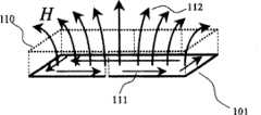
首先,关于该f1,由于根据式(1),天线的线路长对于载波的波长充分短,因此如图2所示,天线线路上的电流分布110几乎均匀。这时,沿着构成天线101的布线(导体线路)流过电流111,由此,由天线101的环所形成的开口部分发生磁场H(磁力线112)。由此,通过在读取装置:R/W(读出器/写入器,未图示)中设置的螺旋天线与天线101之间发生的互感,进行电力传输或者通信信号的存取(收发)。First, regarding this f1, since the antenna line length is sufficiently short for the wavelength of the carrier wave according to Equation (1), the
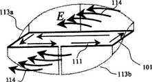
另一方面,关于f2,由于根据式(2),螺旋形天线101的每一圈的长度与波长相当,因此如图3所示,天线布线上的电流分布113在中途翻转相位。这时,通过把IC(集成电路元件)102设置在天线的长边方向的中心附近,上述电流分布在长边方向的一条边上表现正的相位113a,在另一方表现负的相位113b。如果把电流波形113视为正弦波,则在长边方向的一条边上出现从第1象限到第2象限的波形,在其另一条边上出现从第3象限到第4象限的波形,判断为相位相互反相。这时,正相位的电流分布113a在电流朝向的接线方向发生电场E(以下,把电力线114改称为电场),而负相位的电流分布113b在与电流朝向相反方向的接线方向发生电场114。发生这些电场114或者由该电场114感应的电流111流过布线(导体线路)的方向由于在其长边方向的一条边和另一条边中是相反方向,因此分别产生的电场114成为同相,相互增强。由此,螺旋形天线101也具有作为偶极子天线的有效的增益。这一点基本上与折返偶极天线同样发生。但是,为了用顺序(例如,在图1那样的同轴上)配置而且连接具有这种构造(折返偶极子构造)的多条导体线路制作成螺旋形的天线实现上述的作用,必须克服该多条导体线路的长度针对每一圈是不同的这样的课题。这是在如图1所示那样相互不交差地配置构成螺旋形天线101的多条导体线路方面必然产生的课题,为了解决该课题,需要考察以下的条件。On the other hand, regarding f2, since the length of each turn of the
(A)最外周的布线具有与载波的波长相当长度的情况(A) When the outermost wiring has a length corresponding to the wavelength of the carrier wave
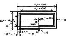
在顺序连接具有图1所示的折返偶极子构造的N条(这里N=3)导体线路构成的方形螺旋天线101中,把位于其最外周的布线(导体线路)的长边的长度(天线长边方向外径)105记为Lxo,把短边的长度(天线短边方向外径)103记为Lyo。另外,把导体线路的邻接一对线路离开的距离(天线布线的间隔)107在其长边方向以及短边方向的每一个中都记为p。这时,位于方形螺旋天线101的最外周的导体线路的长度L1成为“L1=2×(Lxo+Lyo)”,从最该外周起位于第n圈的导体线路的长度(线路长)Ln成为“Ln=2×(Lxo+Lyo-8np)”。In the square
当方形螺旋天线101作为偶极天线发挥功能时,在其长边接收或者发送波长λ的载波。这里论及的条件表现为“L1=λ”,方形螺旋天线101的长边即使在成为最长的位于最外周的导体线路中也不满λ/2。When the square
这里,在沿着导体线路的长边方向延伸部分的中央(错开了一半的位置)处,如果其电流分布113产生相位翻转,则该部分在作为偶极天线的载波发射方面没有贡献,如果偏移得更多,则使发射效率降低。从而,使得在沿着其短边方向延伸的部分中引起构成方形螺旋天线101的导体线路中的电流分布113的相位翻转。Here, if the current distribution 113 at the center (half-staggered position) of the part extending along the long side of the conductor line has a phase inversion, then this part does not contribute to the carrier wave emission as a dipole antenna. Moving it further reduces the emission efficiency. Thereby, the phase inversion of the current distribution 113 in the conductor line constituting the square
为此,方形螺旋天线101的圈数N(导体线路的数量)与其每一圈(导体线路)隔开的间隔最好满足以下的公式。For this reason, the number of turns N (number of conductor lines) of the square
【数3】【Number 3】
通过满足该关系,按照在允许每一条中的电流分布113的相位翻转的范围抑制沿着位于最外周的导体线路和位于最内周的导体线路的每一条中的长边方向延伸的部分的位置以及长度,或者,在沿着各个短边方向延伸的部分中引起相位翻转,确保方形螺旋天线101作为偶极天线的功能。上述式(3)的关系在图1所示的方形螺旋天线中也近似地记为“(N-1)×8p<λ/2”。另外,天线长边方向外径Lxo也可以大于λ/4,天线短边方向外径Lyo也可以小于λ/4。By satisfying this relationship, the position of the portion extending along the long-side direction in each of the conductor line located on the outermost circumference and the conductor line located on the innermost circumference is suppressed within the range allowing phase inversion of the current distribution 113 in each and length, or, causing phase inversion in portions extending along the respective short-side directions, ensures the function of the square
(B)最内周的布线具有与载波的波长相当长度的情况(B) When the innermost wiring has a length corresponding to the wavelength of the carrier
在图1所示的方形螺旋天线101中,把位于其最内周的布线(导体线路)的长边的长度(天线长边方向内径)106记为Lxi,把短边的长度(天线短边方向内径)104记为Lyi时,位于其最内周的导体线路的长度L2成为“L2=2×(Lxi+Lyi)”,从该内周到位于第n圈的导体线路的长度(线路长)Ln成为“Ln=2×(Lxi+Lyi+8np)”。方形螺旋天线101作为偶极天线,在其长边接收或者发送波长λ的载波。在此论及的条件由于成为“L2=λ”,因此方形螺旋天线101的长边虽然在位于最内周的导体线路中不满λ/2,但是在位于比其外周一侧的导体线路中不否认有可能超过λ/2。In the square
因此,与情况B相同,方形螺旋天线101的圈数N与每一圈隔开的间隔最好满足式(3)。另外,与位于最内周的导体线路邻接的其它导体线路(从该内周到位于第1圈的导体线路)的长边的长度最好小于λ/2。Therefore, as in the case B, the number N of turns of the square
(C)从方形螺旋天线向IC的馈电点(C) Feed point from the square helical antenna to the IC
从方形螺旋天线向IC的馈电点最好设置在位于其最外周的导体线路的端部,进而,最好在该位置设置位于其最内周的导体线路的端部。该馈电点可以设置在方形螺旋天线的长边方向的长度(例如,图1所示的天线长边方向外径:Lxo)的中点,但也可以从该中点沿着长边方向偏移一些。对于方形螺旋天线的长边方向的中心(中点)的IC搭载位置(馈电点)的偏移109的值dx例如允许小于等于“∑8np |n=1~N”的范围。另外,在图1所示的方形螺旋天线中,能够规定为近似地小于等于“(N-1)×8p”。The feeding point from the square helical antenna to the IC is preferably provided at the end of the conductor line located on the outermost circumference thereof, and further, the end portion of the conductor line located on the innermost circumference thereof is preferably provided at this position. The feed point can be set at the midpoint of the length of the square helical antenna in the longitudinal direction (for example, the outer diameter of the antenna in the longitudinal direction shown in FIG. 1: Lxo), but it can also be offset from the midpoint along the longitudinal direction Move some. The value dx of the offset 109 of the IC mounting position (feeding point) with respect to the center (midpoint) in the longitudinal direction of the square helical antenna allows, for example, a range equal to or less than "Σ8np |n=1 to N". In addition, in the square helical antenna shown in FIG. 1 , it can be specified to be approximately equal to or smaller than "(N-1)×8p".
成为馈电点的位置,换句话讲,由于位于最外周的导体线路沿着其长边方向延长的一条边为末端的位置(或者其附近),因此影响沿着该导体线路的长边方向产生的电流波形。然而,通过把馈电点位置设置在该长边方向的中点或者从中点离开规定距离的范围内,对于电流的影响抑制为可以忽视的程度。这里记载的所谓规定距离的范围内,也可以是把形成方形螺旋天线的平面中的「位于最外周的导体线路与位于最内周的导体线路的位置偏移」的最大值作为上限的范围。The position that becomes the feed point, in other words, since the conductor line located at the outermost periphery extends along its long side direction as the terminal position (or its vicinity), it affects the long side direction of the conductor line The resulting current waveform. However, by setting the position of the feeding point at the midpoint in the longitudinal direction or within a predetermined distance from the midpoint, the influence on the current is suppressed to a negligible level. The range of the so-called predetermined distance described here may be a range with the maximum value of "the positional deviation between the outermost conductor line and the innermost conductor line" in the plane forming the square helical antenna as an upper limit.
鉴于上述的(A)以及(B)的各情况,则在体现本发明的信号处理电路时,作为方形螺旋天线的设计指导,推荐满足以下的条件。In view of the above (A) and (B), when embodying the signal processing circuit of the present invention, it is recommended that the following conditions be satisfied as a design guideline for the square helical antenna.
[数4][number 4]
2×(Lxi+Lyi)<λ2<2×(Lxo+Lyo) ......(4)2×(Lxi+Lyi)<λ2<2×(Lxo+Lyo) …(4)
另外,从在方形螺旋天线的长边方向防止电流的相位翻转的观点出发,最好使天线长边方向内径Lxi小于λ/2。In addition, from the viewpoint of preventing the phase inversion of the current in the longitudinal direction of the square helical antenna, it is preferable to make the inner diameter Lxi in the longitudinal direction of the antenna smaller than λ/2.
应用例Application example
作为以上所说明的本发明的信号处理电路的应用例,叙述图4所示的非接触IC卡,图5所示的标签(IC标签)。As an application example of the signal processing circuit of the present invention described above, the non-contact IC card shown in FIG. 4 and the tag (IC tag) shown in FIG. 5 will be described.
如上所述,本发明的信号处理电路具备包括RF电路的IC和平面线圈即方形螺旋天线,该方形螺旋天线具有至少进行利用两个载波频率的通信的突出特征。在应用了该特征的非接触IC卡或者标签的任一个中,两个载波频率的一个处在HF频带(一般是3~30MHz的频带,普及利用13.56MHz),另一个位于UHF频带(一般是300~3000MHz的频带,作为例外也包括5.8GHz)。从而,后者的载波频率大于等于前者频率的100倍。As described above, the signal processing circuit of the present invention includes an IC including an RF circuit and a square helical antenna that is a planar coil, which has a prominent feature of performing communication using at least two carrier frequencies. In any of the non-contact IC cards or tags that apply this feature, one of the two carrier frequencies is in the HF frequency band (generally the frequency band of 3-30MHz, and 13.56MHz is commonly used), and the other is in the UHF frequency band (generally the frequency band of 3-30MHz). The frequency band of 300-3000 MHz includes 5.8 GHz as an exception). Thus, the carrier frequency of the latter is greater than or equal to 100 times that of the former.
方形螺旋天线101作为环天线通过HF频带的载波(以下,称为第1频率的载波),向信号处理电路具备的IC(集成电路)102供给来自外部装置的电力,取入信息,或者把来自IC102的信息发送到外部装置。另外,方形螺旋天线101作为偶极天线,通过UHF频带的载波(以下,记为第2频率的载波),向信号处理电路中具备的IC(集成电路)102供给来自外部装置的电力,取入信息,或者把来自IC102的信息传送到外部装置。如果把第1频率取为在作为非接触卡或者标签已知的RFID中广泛使用的13.56MHz,则与此相对应的波长成为大约22m。而如果把第2频率设定在860~960MHz的频带,则其波长为30~35cm的范围,如果设定为2.45GHz,则其波长成为大约12cm。在关于方形螺旋天线的形状的上述考察时,形成串联连接5条平均长度33cm的导体线路形成方形螺旋天线101,制作接收第1频率:13.56MHz的载波和比该第1频率高的第2频率:860MHz的载波的信号处理电路时,方形螺旋天线101的线路长L成为165cm,比第1频率的波长短。另外,如果使方形螺旋天线101的最外周的导体线路的长边L为12.5cm,短边为4.5cm,则与比第1频率的波长短的第2频率的波长(大约35cm)相对应的电流的相位在该长边翻转的概率也降低。在接收第1频率:13.56MHz的载波和第2频率:2.45GHz的载波的信号处理电路中,方形螺旋天线101更小,收入到信用卡中。The square
在图4(a)中表示作为具备接收第1频率:13.56MHz的载波和第2频率:2.45GHz的载波的信号处理电路的非接触IC卡200所形成的信用卡的概略图。在图4(a)中,如果把方形螺旋天线101的下边记为第1边,把左边记为第2边(与第1边交差并且比第1边短),把上边记为第3边(与第1边相对并且与第2边交差,并且比第2边长),把右边记为第4边(与第2边相对,并且与第1边以及第3边交差,并且比第1边以及第3边短),则该方形螺旋天线101串联连接并形成其两端(第1端部和第2端部)位于第1边,而且与该两端的一方(第1端部)相比较,另一方(第2端部)位于方形螺旋天线101的内周一侧的3条导体线路1a~1c。导体线路1a~1c的每一条从其第1端部起,顺序经过上述方形螺旋天线101的第2边、第3边以及第4边延伸,返回到第1边,在其第2端部终止。位于最外周的导体线路1a的第1端部成为连接到IC(这里是102a、102b)的馈电点121的一个,该第2端部连接到与其邻接的导体线路1b的第1端部。从外周起位于第1圈的导体线路1b的第2端连接到与其邻接的导体线路1c的第1端部。位于最内周的导体线路1c的第2端部成为上述馈电点121的另一个。这些导体线路1a~1c一起印刷到成为非接触IC卡的基体材料201的树脂基板上,而也可以把印刷了导体线路1a~1c的树脂膜粘贴到基体材料201的主面上。FIG. 4( a ) shows a schematic diagram of a credit card formed as a
在图4(a)所示的非接触IC卡中,不是使搭载在其中的集成电路元件如图1所示的IC那样分别响应第1频率以及第2频率的载波的混合型,而是分为响应第1频率的第1集成电路102a和响应第2频率的第2集成电路102b。另外,为了防止由第1频率的载波引起的第2集成电路102b的误动作,或者由第2频率的载波引起的第1集成电路102a的误动作,在馈电点121、第1集成电路102a以及第2集成电路102b之间设置分波电路120。In the non-contact IC card shown in FIG. 4(a), it is not a hybrid type in which the integrated circuit elements mounted therein respond to carrier waves of the first frequency and the second frequency as in the IC shown in FIG. These are the first
图4(b)是表示分波电路120的一个例子的概略图。分波电路120作为在由铌酸锂(LiNbO3)等压电性材料构成的基体材料130的主面上形成了梳形的电极123a~123c、124a~124c的2个表面弹性波(Surface Acoustic Wave,SAW)器件的谐振器而形成,各个输入电极123a、124a连接到从导体线路1a上连接的馈电点121a以及导体线路1c上连接的馈电点121b延伸的馈电线122。具备梳形电极123a~123c的SAW谐振器起到使第1频率的信号通过输出电极123b而不使第2频率的信号通过的带通滤波器(低通滤波器)123的作用,具备梳形电极124a~124c的SAW谐振器起到使第2频率的信号通过输出电极124b而不使第1频率通过的信号的带通滤波器(高通滤波器)124的作用。因此,与在带通滤波器123上设置的梳形电极123a~123c的间隔相比较,在带通滤波器124上设置的梳形电极124a~124c的间隔反映所通过的信号的波长而狭窄。带通滤波器123的输出电极123b连接到第1集成电路102a,带通滤波器124的输出电极124b连接到第2集成电路102b。FIG. 4( b ) is a schematic diagram showing an example of the
在图4(b)中,由图4(a)所示的导体线路1a~1c构成的方形螺旋天线101为了作图上的方便,简略描绘为一条导体线路1。形成了分波电路120的基体材料130埋入到在成为非接触IC卡的基体材料201的树脂基板上形成的凹槽中,用黑色的四方块表示的2个馈电点121a、121b连接到形成在基体材料103上的馈电线122。In FIG. 4( b ), the square
图4(c)表示使用了把图4(a)所示的第1集成电路102a和第2集成电路102b做成一体的集成电路元件102的非接触IC卡的概略图,在馈电点121与集成电路元件102之间设置分波电路120。在集成电路元件120的下面(安装面)上,设置接收第1频率的信号的电极120a和接收第2频率的信号的电极120b,通过面朝下安装到基体材料130上,电极120a连接到带通滤波器123的输出电极123b,电极120b连接到带通滤波器124的输出电极124b。Fig. 4 (c) shows the schematic diagram that has used the non-contact IC card of the
在图5(a)中,表示具备接收第1频率:13.56MHz的载波和第2频率:900MHz的载波的信号处理电路的标签(IC标签)300的概略图。该标签形成在由环氧树脂或者聚对苯二甲酸乙二脂(PET)等构成的可挠性基体材料301上,以便粘贴到包裹等发送物上,方形螺旋天线101印刷在例如该基体材料301的主面上。方形螺旋天线101串联连接2条导体线路1a、1b,鉴于通过它们收发的第2频率的载波为:33cm,形成为满足其天线长边的长边方向外径(图1所示的长度Lxo)小于等于16.6cm(不满载波波长的1/2),天线长边方向内径(图1所示的长度Lxi)大于等于8.4cm(超过载波波长的1/4),天线短边方向外径(图1所示的长度Lyo)小于等于8.3cm(不满载波波长的1/4)。对于第2频率的载波波长λ2,方形螺旋天线101的总长由于小于N×{(2×λ2/2)+(2×λ2/4)}=3Nλ2/2(其中,N是导体线路的数量)的值,因此像微带线那样使天线布线宽度108(参照图1,导体线路的宽度w)狭窄,N只要不是大于等于44条,则就对于具有波长:22.1m的第1频率的载波的收发不带来妨碍。In FIG. 5( a ), a schematic diagram of a tag (IC tag) 300 including a signal processing circuit for receiving a first frequency: 13.56 MHz carrier and a second frequency: 900 MHz is shown. The label is formed on a
在图5(a)所示的标签中,也与图4(a)所示的非接触IC卡相同,搭载响应第1频率的第1集成电路102a和响应第2频率的第2集成电路102b,在这些集成电路102a、102b与设置在螺旋天线101两端的馈电点121之间,设置形成在基体材料103上的分波电路。In the tag shown in FIG. 5(a), the same as the non-contact IC card shown in FIG. 4(a), the first
图5(b)表示设置在图5(a)所示的标签中的分波电路120的电路的一个例子,图5(c)表示该标签的剖面并包含分波电路120的一部分。在图5(b)中,作为一条导体线路1描绘图5(a)所示的由导体线路1a、1b构成的方形螺旋天线101。图5(b)所示接地电位的符号指的是标签电路中的「基准电位」,描绘成与其连接的元件也可以不接地。与从设置在方形螺旋天线101的最外周的一端上的馈电点121a向分波电路120延伸的馈电线122相比较,从设置在最内周面的另一端上的馈电点121b向分波电路120延伸的馈电线122中,设置肖特基势垒二极管122a或者电容122b。肖特基势垒二极管122a表示解调由标签接收的信号或者调制从标签发送的信号的功能。FIG. 5( b ) shows an example of the circuit of the
图5(b)所示的分波电路120具备与响应第1频率的第1集成电路102a上连接的带通滤波器123和响应第2频率的第2集成电路102b上连接的带通滤波器124。带通滤波器123具备具有电感123d以及电容123e的谐振电路,起到通过第1频率的信号并且阻断第2频率的信号的低通滤波器的作用。带通滤波器124具备具有电容124d、124e以及电感124f的谐振电路,起到通过第2频率的信号并且阻断第1频率的信号的高通滤波器的作用。The
分波电路120的电感123d、124f以及电容123e、124d、124e如图5(c)所示的电感123d那样,把构成其各个元件导体层形成在基体材料130上。为了提高标签的可挠性,基体材料130与标签的基体材料301相同,可以用环氧树脂或者聚对苯二甲酸乙酯(PET)等膜形成,也可以用比其更易于挠动的材料的膜形成。图5(c)所示的电感123d把在基体材料130的两个主面上印刷的导体层131(涂黑表示)通过形成在该基体材料130上的通孔电连接,形成线圈形。导体层131的一个电连接到第1集成电路102a上形成的电极(焊盘)126上,在带通滤波器123与第1集成电路102a之间形成信号路径。另外,第1集成电路102a的电极126用「空白」示出的一方表示在集成电路与分波电路120的信号收发中没有贡献的虚设的焊盘。The
在基体材料130上,还形成构成设置在馈电线122上的电容122b的导体层,在该主面的一方(与基体材料301的结合面相反的一侧)上实际安装肖特基势垒二极管122a。作为分别贯通基体材料301及基体材料130的通孔形成从馈电点121a、121b延伸的馈电线122。用保护膜302覆盖形成基体材料301的方形螺旋天线101的主面,在该保护膜302的上面涂覆用于把标签粘贴到小包等上的粘接剂(未图示)。On the
在以上说明的本发明的信号处理电路、使用了该电路的非接触IC卡以及标签(RFID)中的任一个,由于都能够用其所具备的一个天线收发频带相互不同的多个载波,因此促进其小型化或者降低制造成本。另外,由于不需要在一个电路(装置)上设置多个天线,因此也没有天线之间干扰的担心。从而,顾及把RFID的输出的上限抑制为很低的HF频带的载波和提高来自RFID的输出的UHF频带的载波所构筑的RFID系统能够用具备一个天线的RFID实用化。换句话讲,能够使该系统使用者不必持有多片RFID(非接触IC卡以及/或者标签),另外不必新制作搭载了多个天线的RFID,就能够实际使用该系统。In any of the signal processing circuit of the present invention described above, the non-contact IC card and the tag (RFID) using the circuit, since it is possible to transmit and receive a plurality of carriers having different frequency bands with one antenna provided therein, Promote its miniaturization or reduce its manufacturing cost. In addition, since there is no need to install a plurality of antennas on one circuit (device), there is no concern about interference between antennas. Therefore, an RFID system constructed in consideration of a carrier of the HF band for suppressing the upper limit of the output of RFID to a very low level and a carrier of the UHF band for increasing the output from the RFID can be put into practical use with an RFID having one antenna. In other words, users of the system can actually use the system without having multiple RFIDs (non-contact IC cards and/or tags), and without newly manufacturing RFIDs equipped with multiple antennas.
Claims (13)
Applications Claiming Priority (3)
| Application Number | Priority Date | Filing Date | Title |
|---|---|---|---|
| JP2005130733 | 2005-04-28 | ||
| JP2005-130733 | 2005-04-28 | ||
| JP2005130733AJP4529786B2 (en) | 2005-04-28 | 2005-04-28 | Signal processing circuit and non-contact IC card and tag using the same |
Publications (2)
| Publication Number | Publication Date |
|---|---|
| CN1855131A CN1855131A (en) | 2006-11-01 |
| CN100433056Ctrue CN100433056C (en) | 2008-11-12 |
Family
ID=36754216
Family Applications (1)
| Application Number | Title | Priority Date | Filing Date |
|---|---|---|---|
| CNB2006100772498AExpired - Fee RelatedCN100433056C (en) | 2005-04-28 | 2006-04-28 | Signal processing circuit and non-contrct ic card using same and tag |
Country Status (5)
| Country | Link |
|---|---|
| US (1) | US7439933B2 (en) |
| EP (1) | EP1720215B1 (en) |
| JP (1) | JP4529786B2 (en) |
| CN (1) | CN100433056C (en) |
| DE (1) | DE602006016670D1 (en) |
Families Citing this family (107)
| Publication number | Priority date | Publication date | Assignee | Title |
|---|---|---|---|---|
| US7667589B2 (en) | 2004-03-29 | 2010-02-23 | Impinj, Inc. | RFID tag uncoupling one of its antenna ports and methods |
| USD578114S1 (en) | 2004-03-29 | 2008-10-07 | Impinj, Inc. | Radio frequency indentification tag antenna assembly |
| USD587691S1 (en) | 2004-03-29 | 2009-03-03 | Impinj, Inc. | Radio frequency identification tag antenna assembly |
| US7528728B2 (en) | 2004-03-29 | 2009-05-05 | Impinj Inc. | Circuits for RFID tags with multiple non-independently driven RF ports |
| US7423539B2 (en)* | 2004-03-31 | 2008-09-09 | Impinj, Inc. | RFID tags combining signals received from multiple RF ports |
| USD586336S1 (en) | 2004-12-30 | 2009-02-10 | Impinj, Inc. | Radio frequency identification tag antenna assembly |
| US7519328B2 (en) | 2006-01-19 | 2009-04-14 | Murata Manufacturing Co., Ltd. | Wireless IC device and component for wireless IC device |
| USD546821S1 (en)* | 2006-02-17 | 2007-07-17 | Impinj, Inc. | Radio frequency identification tag antenna assembly |
| US9064198B2 (en) | 2006-04-26 | 2015-06-23 | Murata Manufacturing Co., Ltd. | Electromagnetic-coupling-module-attached article |
| CN101467209B (en) | 2006-06-30 | 2012-03-21 | 株式会社村田制作所 | Optical disc |
| JP4466689B2 (en)* | 2006-08-31 | 2010-05-26 | 株式会社カシオ日立モバイルコミュニケーションズ | Antenna and portable electronic device |
| WO2008050535A1 (en) | 2006-09-26 | 2008-05-02 | Murata Manufacturing Co., Ltd. | Electromagnetically coupled module and article with electromagnetically coupled module |
| US7922961B2 (en)* | 2006-11-10 | 2011-04-12 | Rexam Healthcare Packaging Inc. | Molded plastic container having insert-molded insert and method of manufacture |
| US7850893B2 (en) | 2006-12-01 | 2010-12-14 | Rexam Healthcare Packaging Inc. | Molded plastic container and preform having insert-molded RFID tag |
| WO2008103870A1 (en)* | 2007-02-23 | 2008-08-28 | Newpage Wisconsin System Inc. | Multifunctional paper identification label |
| US8235299B2 (en) | 2007-07-04 | 2012-08-07 | Murata Manufacturing Co., Ltd. | Wireless IC device and component for wireless IC device |
| EP2138962B1 (en) | 2007-04-26 | 2012-01-04 | Murata Manufacturing Co. Ltd. | Wireless ic device |
| US8174454B2 (en)* | 2007-05-07 | 2012-05-08 | Infineon Technologies Ag | Dual-band antenna |
| EP2148449B1 (en) | 2007-05-11 | 2012-12-12 | Murata Manufacturing Co., Ltd. | Wireless ic device |
| GB0709313D0 (en)* | 2007-05-15 | 2007-06-20 | Siemens Ag | RFID reader |
| DE102007029083B4 (en)* | 2007-06-21 | 2019-05-16 | ASTRA Gesellschaft für Asset Management mbH & Co. KG | Card carrier with Detektierplättchen |
| EP2166617B1 (en) | 2007-07-09 | 2015-09-30 | Murata Manufacturing Co. Ltd. | Wireless ic device |
| EP2166490B1 (en)* | 2007-07-17 | 2015-04-01 | Murata Manufacturing Co. Ltd. | Wireless ic device and electronic apparatus |
| US20090021352A1 (en)* | 2007-07-18 | 2009-01-22 | Murata Manufacturing Co., Ltd. | Radio frequency ic device and electronic apparatus |
| CN102915462B (en) | 2007-07-18 | 2017-03-01 | 株式会社村田制作所 | Wireless IC device |
| JP5146872B2 (en)* | 2007-07-24 | 2013-02-20 | Necアクセステクニカ株式会社 | Non-contact IC card, portable terminal device, activation control method, and activation control program |
| KR100928119B1 (en) | 2007-10-30 | 2009-11-24 | 삼성에스디아이 주식회사 | Printed Circuit Board and Secondary Battery Using the Same |
| US8929805B2 (en) | 2007-10-30 | 2015-01-06 | Nationz Technologies Inc. | System, method, and device for radio frequency communication |
| JP4462388B2 (en) | 2007-12-20 | 2010-05-12 | 株式会社村田製作所 | Wireless IC device |
| CN103500875B (en)* | 2007-12-26 | 2015-12-02 | 株式会社村田制作所 | Antenna assembly and Wireless IC device |
| EP2251934B1 (en)* | 2008-03-03 | 2018-05-02 | Murata Manufacturing Co. Ltd. | Wireless ic device and wireless communication system |
| WO2009110382A1 (en)* | 2008-03-03 | 2009-09-11 | 株式会社村田製作所 | Composite antenna |
| EP2256861B1 (en)* | 2008-03-26 | 2018-12-05 | Murata Manufacturing Co., Ltd. | Radio ic device |
| KR100978271B1 (en)* | 2008-04-01 | 2010-08-26 | 엘에스산전 주식회사 | RFID tag using built-in antenna and RFID system using same |
| EP2264831B1 (en)* | 2008-04-14 | 2020-05-27 | Murata Manufacturing Co. Ltd. | Radio ic device, electronic device, and method for adjusting resonance frequency of radio ic device |
| EP2284949B1 (en)* | 2008-05-21 | 2016-08-03 | Murata Manufacturing Co. Ltd. | Wireless ic device |
| WO2009142068A1 (en)* | 2008-05-22 | 2009-11-26 | 株式会社村田製作所 | Wireless ic device and method for manufacturing the same |
| WO2009145007A1 (en) | 2008-05-26 | 2009-12-03 | 株式会社村田製作所 | Wireless ic device system and method for authenticating wireless ic device |
| KR101148534B1 (en)* | 2008-05-28 | 2012-05-21 | 가부시키가이샤 무라타 세이사쿠쇼 | Wireless ic device and component for a wireless ic device |
| JP4557186B2 (en)* | 2008-06-25 | 2010-10-06 | 株式会社村田製作所 | Wireless IC device and manufacturing method thereof |
| WO2010001469A1 (en) | 2008-07-02 | 2010-01-07 | 三菱電機株式会社 | Wireless communication device |
| WO2010001987A1 (en)* | 2008-07-04 | 2010-01-07 | 株式会社村田製作所 | Wireless ic device |
| EP2320519B1 (en)* | 2008-08-19 | 2017-04-12 | Murata Manufacturing Co., Ltd. | Wireless ic device and method for manufacturing same |
| JP5429182B2 (en)* | 2008-10-24 | 2014-02-26 | 株式会社村田製作所 | Wireless IC device |
| JP4525869B2 (en)* | 2008-10-29 | 2010-08-18 | 株式会社村田製作所 | Wireless IC device |
| JP4605318B2 (en)* | 2008-11-17 | 2011-01-05 | 株式会社村田製作所 | Antenna and wireless IC device |
| CN103500873B (en) | 2009-01-09 | 2016-08-31 | 株式会社村田制作所 | Wireless ic device and wireless ic module |
| CN102204011B (en)* | 2009-01-16 | 2013-12-25 | 株式会社村田制作所 | High frequency device and wireless IC device |
| EP2385580B1 (en) | 2009-01-30 | 2014-04-09 | Murata Manufacturing Co., Ltd. | Antenna and wireless ic device |
| KR101023884B1 (en)* | 2009-02-18 | 2011-03-22 | 삼성에스디아이 주식회사 | Battery pack |
| JP5282896B2 (en)* | 2009-03-12 | 2013-09-04 | 日本電気株式会社 | Antenna device |
| JP5282898B2 (en)* | 2009-03-13 | 2013-09-04 | 日本電気株式会社 | Antenna device |
| JP5510450B2 (en) | 2009-04-14 | 2014-06-04 | 株式会社村田製作所 | Wireless IC device |
| EP2568534A3 (en) | 2009-04-21 | 2014-05-14 | Murata Manufacturing Co., Ltd. | Antenna devie and method of setting resonant frequency of antenna device |
| CN102449846B (en) | 2009-06-03 | 2015-02-04 | 株式会社村田制作所 | Wireless IC device and production method thereof |
| US9004360B2 (en)* | 2009-06-10 | 2015-04-14 | Infineon Technologies Ag | Contactless communication via a plurality of interfaces |
| JP5516580B2 (en) | 2009-06-19 | 2014-06-11 | 株式会社村田製作所 | Wireless IC device and method for coupling power feeding circuit and radiation plate |
| JP5182431B2 (en) | 2009-09-28 | 2013-04-17 | 株式会社村田製作所 | Wireless IC device and environmental state detection method using the same |
| JP5201270B2 (en) | 2009-09-30 | 2013-06-05 | 株式会社村田製作所 | Circuit board and manufacturing method thereof |
| JP5304580B2 (en) | 2009-10-02 | 2013-10-02 | 株式会社村田製作所 | Wireless IC device |
| CN102576939B (en) | 2009-10-16 | 2015-11-25 | 株式会社村田制作所 | Antenna and wireless ic device |
| JP5418600B2 (en) | 2009-10-27 | 2014-02-19 | 株式会社村田製作所 | Transceiver and RFID tag reader |
| WO2011055702A1 (en) | 2009-11-04 | 2011-05-12 | 株式会社村田製作所 | Wireless ic tag, reader/writer, and information processing system |
| JP5327334B2 (en) | 2009-11-04 | 2013-10-30 | 株式会社村田製作所 | Communication terminal and information processing system |
| WO2011055701A1 (en) | 2009-11-04 | 2011-05-12 | 株式会社村田製作所 | Communication terminal and information processing system |
| CN104617374B (en) | 2009-11-20 | 2018-04-06 | 株式会社村田制作所 | Mobile communication terminal |
| GB2488450B (en) | 2009-12-24 | 2014-08-20 | Murata Manufacturing Co | Antenna and mobile terminal |
| WO2011108340A1 (en) | 2010-03-03 | 2011-09-09 | 株式会社村田製作所 | Wireless communication module and wireless communication device |
| JP5403146B2 (en) | 2010-03-03 | 2014-01-29 | 株式会社村田製作所 | Wireless communication device and wireless communication terminal |
| CN102576940B (en) | 2010-03-12 | 2016-05-04 | 株式会社村田制作所 | Wireless communication devices and metal article processed |
| JP5370581B2 (en)* | 2010-03-24 | 2013-12-18 | 株式会社村田製作所 | RFID system |
| WO2011122163A1 (en) | 2010-03-31 | 2011-10-06 | 株式会社村田製作所 | Antenna and wireless communication device |
| JP5299351B2 (en) | 2010-05-14 | 2013-09-25 | 株式会社村田製作所 | Wireless IC device |
| JP5170156B2 (en) | 2010-05-14 | 2013-03-27 | 株式会社村田製作所 | Wireless IC device |
| WO2012005278A1 (en) | 2010-07-08 | 2012-01-12 | 株式会社村田製作所 | Antenna and rfid device |
| GB2537773A (en) | 2010-07-28 | 2016-10-26 | Murata Manufacturing Co | Antenna apparatus and communication terminal instrument |
| JP5423897B2 (en) | 2010-08-10 | 2014-02-19 | 株式会社村田製作所 | Printed wiring board and wireless communication system |
| JP5234071B2 (en) | 2010-09-03 | 2013-07-10 | 株式会社村田製作所 | RFIC module |
| JP5630506B2 (en) | 2010-09-30 | 2014-11-26 | 株式会社村田製作所 | Wireless IC device |
| WO2012050037A1 (en) | 2010-10-12 | 2012-04-19 | 株式会社村田製作所 | Antenna apparatus and communication terminal apparatus |
| CN102971909B (en) | 2010-10-21 | 2014-10-15 | 株式会社村田制作所 | Communication terminal device |
| WO2012093541A1 (en) | 2011-01-05 | 2012-07-12 | 株式会社村田製作所 | Wireless communication device |
| CN103299325B (en) | 2011-01-14 | 2016-03-02 | 株式会社村田制作所 | RFID chip packaging and RFID tags |
| CN103119786B (en) | 2011-02-28 | 2015-07-22 | 株式会社村田制作所 | Wireless communication device |
| WO2012121185A1 (en) | 2011-03-08 | 2012-09-13 | 株式会社村田製作所 | Antenna device and communication terminal apparatus |
| WO2012137717A1 (en) | 2011-04-05 | 2012-10-11 | 株式会社村田製作所 | Wireless communication device |
| WO2012141070A1 (en) | 2011-04-13 | 2012-10-18 | 株式会社村田製作所 | Wireless ic device and wireless communication terminal |
| WO2012157596A1 (en) | 2011-05-16 | 2012-11-22 | 株式会社村田製作所 | Wireless ic device |
| KR101338173B1 (en) | 2011-07-14 | 2013-12-06 | 가부시키가이샤 무라타 세이사쿠쇼 | Wireless communication device |
| WO2013011856A1 (en) | 2011-07-15 | 2013-01-24 | 株式会社村田製作所 | Wireless communication device |
| CN204189963U (en) | 2011-07-19 | 2015-03-04 | 株式会社村田制作所 | Antenna assembly and communication terminal |
| WO2013035821A1 (en) | 2011-09-09 | 2013-03-14 | 株式会社村田製作所 | Antenna device and wireless device |
| TWI488367B (en)* | 2011-11-15 | 2015-06-11 | Ind Tech Res Inst | Rfid tag antenna |
| US9484629B2 (en)* | 2011-11-22 | 2016-11-01 | Microsoft Technology Licensing, Llc | Multi-use antenna |
| JP5344108B1 (en) | 2011-12-01 | 2013-11-20 | 株式会社村田製作所 | Wireless IC device and manufacturing method thereof |
| EP2688145A1 (en) | 2012-01-30 | 2014-01-22 | Murata Manufacturing Co., Ltd. | Wireless ic device |
| JP5464307B2 (en) | 2012-02-24 | 2014-04-09 | 株式会社村田製作所 | ANTENNA DEVICE AND WIRELESS COMMUNICATION DEVICE |
| CN104487985B (en) | 2012-04-13 | 2020-06-26 | 株式会社村田制作所 | RFID tag inspection method and inspection device |
| JP2014187615A (en)* | 2013-03-25 | 2014-10-02 | Tokai Rika Co Ltd | Antenna device |
| EP3375038A1 (en)* | 2015-11-09 | 2018-09-19 | 3M Innovative Properties Company | Radio frequency circuit with conductive loop |
| FR3046279B1 (en)* | 2015-12-23 | 2019-05-17 | Idemia France | ELECTRONIC WIRELESS COMMUNICATION DEVICE HAVING TWO ELECTRONIC CHIPS AND METHOD OF MANUFACTURING SUCH A DEVICE |
| CN106447013B (en)* | 2016-10-14 | 2023-06-06 | 广州明森科技股份有限公司 | Smart card chip overturning and wire gathering device |
| US11087101B2 (en)* | 2017-11-03 | 2021-08-10 | Pap Investments, Ltd. | Dual frequency NFC/RFID card for self service baggage check and method |
| US10833409B2 (en)* | 2017-12-12 | 2020-11-10 | Alireza Akbarpour | Dual-band magnetic antenna |
| EP3499421A1 (en)* | 2017-12-15 | 2019-06-19 | The Swatch Group Research and Development Ltd | Module with rfid transponder for communicating information to a reading device |
| CN108197516A (en)* | 2017-12-29 | 2018-06-22 | 北京奇虎科技有限公司 | Wireless near field communication card-reading apparatus and system |
| JP7377490B2 (en)* | 2019-11-19 | 2023-11-10 | 大王製紙株式会社 | RFID tag |
Citations (4)
| Publication number | Priority date | Publication date | Assignee | Title |
|---|---|---|---|---|
| JPH05290229A (en)* | 1992-04-06 | 1993-11-05 | Kyodo Printing Co Ltd | Non-contact type IC card and its identification system |
| JP2000260597A (en)* | 1999-03-11 | 2000-09-22 | Nihon Koshuha Co Ltd | High-frequency synthetic device type plasma treatment system |
| JP2004240899A (en)* | 2003-02-10 | 2004-08-26 | Totoku Electric Co Ltd | Hybrid type non-contact IC card |
| JP2004297499A (en)* | 2003-03-27 | 2004-10-21 | Sony Ericsson Mobilecommunications Japan Inc | Communication terminal device |
Family Cites Families (10)
| Publication number | Priority date | Publication date | Assignee | Title |
|---|---|---|---|---|
| US5295029A (en)* | 1990-07-31 | 1994-03-15 | Seagate Technology, Inc. | Disk drive including unitary deck for aligning and supporting axially retractable spindle assembly |
| JP3519520B2 (en)* | 1995-11-09 | 2004-04-19 | 株式会社東芝 | Wireless communication system |
| EP0886232B1 (en)* | 1997-06-20 | 2007-09-05 | Hitachi, Ltd. | Reader and/or writer apparatus, power feeding system, and communication system |
| JP2001067447A (en)* | 1999-08-30 | 2001-03-16 | Mitsumi Electric Co Ltd | Noncontact ic card |
| DE10022107A1 (en)* | 2000-05-08 | 2001-11-15 | Alcatel Sa | Integrated antenna for mobile phones |
| JP2002022861A (en)* | 2000-07-13 | 2002-01-23 | Canon Inc | Electronic equipment with timing device |
| US6295029B1 (en)* | 2000-09-27 | 2001-09-25 | Auden Techno Corp. | Miniature microstrip antenna |
| WO2003041216A2 (en)* | 2001-11-02 | 2003-05-15 | Skycross, Inc. | Dual band spiral-shaped antenna |
| JP2004227046A (en)* | 2003-01-20 | 2004-08-12 | Hitachi Ltd | Portable information equipment |
| JP2005033500A (en)* | 2003-07-14 | 2005-02-03 | Hitachi Ltd | Antenna coil design apparatus and design method |
- 2005
- 2005-04-28JPJP2005130733Apatent/JP4529786B2/ennot_activeExpired - Fee Related
- 2006
- 2006-04-27DEDE602006016670Tpatent/DE602006016670D1/enactiveActive
- 2006-04-27EPEP06008824Apatent/EP1720215B1/ennot_activeNot-in-force
- 2006-04-28CNCNB2006100772498Apatent/CN100433056C/ennot_activeExpired - Fee Related
- 2006-04-28USUS11/412,988patent/US7439933B2/enactiveActive
Patent Citations (4)
| Publication number | Priority date | Publication date | Assignee | Title |
|---|---|---|---|---|
| JPH05290229A (en)* | 1992-04-06 | 1993-11-05 | Kyodo Printing Co Ltd | Non-contact type IC card and its identification system |
| JP2000260597A (en)* | 1999-03-11 | 2000-09-22 | Nihon Koshuha Co Ltd | High-frequency synthetic device type plasma treatment system |
| JP2004240899A (en)* | 2003-02-10 | 2004-08-26 | Totoku Electric Co Ltd | Hybrid type non-contact IC card |
| JP2004297499A (en)* | 2003-03-27 | 2004-10-21 | Sony Ericsson Mobilecommunications Japan Inc | Communication terminal device |
Also Published As
| Publication number | Publication date |
|---|---|
| US20060244676A1 (en) | 2006-11-02 |
| DE602006016670D1 (en) | 2010-10-21 |
| CN1855131A (en) | 2006-11-01 |
| JP2006309476A (en) | 2006-11-09 |
| JP4529786B2 (en) | 2010-08-25 |
| EP1720215A1 (en) | 2006-11-08 |
| EP1720215B1 (en) | 2010-09-08 |
| US7439933B2 (en) | 2008-10-21 |
Similar Documents
| Publication | Publication Date | Title |
|---|---|---|
| CN100433056C (en) | Signal processing circuit and non-contrct ic card using same and tag | |
| JP3879098B2 (en) | Booster antenna for IC card | |
| US8749390B2 (en) | RFID antenna circuit | |
| US8174454B2 (en) | Dual-band antenna | |
| US8006910B2 (en) | Wireless IC device | |
| US9016592B2 (en) | Antenna device and communication terminal apparatus | |
| US8668151B2 (en) | Wireless IC device | |
| US9646242B2 (en) | Booster antenna, contactless chip arrangement, antenna structure and chip arrangement | |
| US9104950B2 (en) | Antenna and wireless IC device | |
| US10396429B2 (en) | Wireless communication device | |
| CN106339746B (en) | Multi-frequency transponder with single antenna | |
| EP2009736A1 (en) | Wireless ic device | |
| EP2077602B1 (en) | Wireless ic device | |
| CN103688409B (en) | Antenna and wireless identification tag | |
| CN103370834B (en) | Wireless communication devices | |
| CN102204112A (en) | Radio communication device | |
| JPWO2019116758A1 (en) | RFID tag and article to which the RFID tag is attached | |
| JPWO2012032974A1 (en) | RFID module and RFID device | |
| US20060055617A1 (en) | Integrated antenna matching network | |
| US8720789B2 (en) | Wireless IC device | |
| CN103814478B (en) | Antennas and Wireless Tags | |
| JP5601247B2 (en) | Antenna and wireless tag |
Legal Events
| Date | Code | Title | Description |
|---|---|---|---|
| C06 | Publication | ||
| PB01 | Publication | ||
| C10 | Entry into substantive examination | ||
| SE01 | Entry into force of request for substantive examination | ||
| C14 | Grant of patent or utility model | ||
| GR01 | Patent grant | ||
| C17 | Cessation of patent right | ||
| CF01 | Termination of patent right due to non-payment of annual fee | Granted publication date:20081112 Termination date:20140428 |