CN100431110C - Method for forming low-dielectric silicon nitride film, semiconductor device and manufacturing process thereof - Google Patents
Method for forming low-dielectric silicon nitride film, semiconductor device and manufacturing process thereofDownload PDFInfo
- Publication number
- CN100431110C CN100431110CCNB018140505ACN01814050ACN100431110CCN 100431110 CCN100431110 CCN 100431110CCN B018140505 ACNB018140505 ACN B018140505ACN 01814050 ACN01814050 ACN 01814050ACN 100431110 CCN100431110 CCN 100431110C
- Authority
- CN
- China
- Prior art keywords
- film
- sinch
- organic
- compound
- plasma
- Prior art date
- Legal status (The legal status is an assumption and is not a legal conclusion. Google has not performed a legal analysis and makes no representation as to the accuracy of the status listed.)
- Expired - Fee Related
Links
Images


Classifications
- H—ELECTRICITY
- H01—ELECTRIC ELEMENTS
- H01L—SEMICONDUCTOR DEVICES NOT COVERED BY CLASS H10
- H01L21/00—Processes or apparatus adapted for the manufacture or treatment of semiconductor or solid state devices or of parts thereof
- H01L21/70—Manufacture or treatment of devices consisting of a plurality of solid state components formed in or on a common substrate or of parts thereof; Manufacture of integrated circuit devices or of parts thereof
- H01L21/71—Manufacture of specific parts of devices defined in group H01L21/70
- H01L21/768—Applying interconnections to be used for carrying current between separate components within a device comprising conductors and dielectrics
- H01L21/76801—Applying interconnections to be used for carrying current between separate components within a device comprising conductors and dielectrics characterised by the formation and the after-treatment of the dielectrics, e.g. smoothing
- H01L21/76829—Applying interconnections to be used for carrying current between separate components within a device comprising conductors and dielectrics characterised by the formation and the after-treatment of the dielectrics, e.g. smoothing characterised by the formation of thin functional dielectric layers, e.g. dielectric etch-stop, barrier, capping or liner layers
- H01L21/76834—Applying interconnections to be used for carrying current between separate components within a device comprising conductors and dielectrics characterised by the formation and the after-treatment of the dielectrics, e.g. smoothing characterised by the formation of thin functional dielectric layers, e.g. dielectric etch-stop, barrier, capping or liner layers formation of thin insulating films on the sidewalls or on top of conductors
- C—CHEMISTRY; METALLURGY
- C23—COATING METALLIC MATERIAL; COATING MATERIAL WITH METALLIC MATERIAL; CHEMICAL SURFACE TREATMENT; DIFFUSION TREATMENT OF METALLIC MATERIAL; COATING BY VACUUM EVAPORATION, BY SPUTTERING, BY ION IMPLANTATION OR BY CHEMICAL VAPOUR DEPOSITION, IN GENERAL; INHIBITING CORROSION OF METALLIC MATERIAL OR INCRUSTATION IN GENERAL
- C23C—COATING METALLIC MATERIAL; COATING MATERIAL WITH METALLIC MATERIAL; SURFACE TREATMENT OF METALLIC MATERIAL BY DIFFUSION INTO THE SURFACE, BY CHEMICAL CONVERSION OR SUBSTITUTION; COATING BY VACUUM EVAPORATION, BY SPUTTERING, BY ION IMPLANTATION OR BY CHEMICAL VAPOUR DEPOSITION, IN GENERAL
- C23C16/00—Chemical coating by decomposition of gaseous compounds, without leaving reaction products of surface material in the coating, i.e. chemical vapour deposition [CVD] processes
- C23C16/22—Chemical coating by decomposition of gaseous compounds, without leaving reaction products of surface material in the coating, i.e. chemical vapour deposition [CVD] processes characterised by the deposition of inorganic material, other than metallic material
- C23C16/30—Deposition of compounds, mixtures or solid solutions, e.g. borides, carbides, nitrides
- C23C16/34—Nitrides
- C23C16/345—Silicon nitride
- H—ELECTRICITY
- H01—ELECTRIC ELEMENTS
- H01L—SEMICONDUCTOR DEVICES NOT COVERED BY CLASS H10
- H01L21/00—Processes or apparatus adapted for the manufacture or treatment of semiconductor or solid state devices or of parts thereof
- H01L21/02—Manufacture or treatment of semiconductor devices or of parts thereof
- H01L21/02104—Forming layers
- H01L21/02107—Forming insulating materials on a substrate
- H01L21/02109—Forming insulating materials on a substrate characterised by the type of layer, e.g. type of material, porous/non-porous, pre-cursors, mixtures or laminates
- H01L21/02205—Forming insulating materials on a substrate characterised by the type of layer, e.g. type of material, porous/non-porous, pre-cursors, mixtures or laminates the layer being characterised by the precursor material for deposition
- H01L21/02208—Forming insulating materials on a substrate characterised by the type of layer, e.g. type of material, porous/non-porous, pre-cursors, mixtures or laminates the layer being characterised by the precursor material for deposition the precursor containing a compound comprising Si
- H01L21/02219—Forming insulating materials on a substrate characterised by the type of layer, e.g. type of material, porous/non-porous, pre-cursors, mixtures or laminates the layer being characterised by the precursor material for deposition the precursor containing a compound comprising Si the compound comprising silicon and nitrogen
- H01L21/02222—Forming insulating materials on a substrate characterised by the type of layer, e.g. type of material, porous/non-porous, pre-cursors, mixtures or laminates the layer being characterised by the precursor material for deposition the precursor containing a compound comprising Si the compound comprising silicon and nitrogen the compound being a silazane
- H—ELECTRICITY
- H01—ELECTRIC ELEMENTS
- H01L—SEMICONDUCTOR DEVICES NOT COVERED BY CLASS H10
- H01L21/00—Processes or apparatus adapted for the manufacture or treatment of semiconductor or solid state devices or of parts thereof
- H01L21/70—Manufacture or treatment of devices consisting of a plurality of solid state components formed in or on a common substrate or of parts thereof; Manufacture of integrated circuit devices or of parts thereof
- H01L21/71—Manufacture of specific parts of devices defined in group H01L21/70
- H01L21/768—Applying interconnections to be used for carrying current between separate components within a device comprising conductors and dielectrics
- H01L21/76801—Applying interconnections to be used for carrying current between separate components within a device comprising conductors and dielectrics characterised by the formation and the after-treatment of the dielectrics, e.g. smoothing
- H01L21/76802—Applying interconnections to be used for carrying current between separate components within a device comprising conductors and dielectrics characterised by the formation and the after-treatment of the dielectrics, e.g. smoothing by forming openings in dielectrics
- H01L21/76807—Applying interconnections to be used for carrying current between separate components within a device comprising conductors and dielectrics characterised by the formation and the after-treatment of the dielectrics, e.g. smoothing by forming openings in dielectrics for dual damascene structures
- H01L21/76808—Applying interconnections to be used for carrying current between separate components within a device comprising conductors and dielectrics characterised by the formation and the after-treatment of the dielectrics, e.g. smoothing by forming openings in dielectrics for dual damascene structures involving intermediate temporary filling with material
- H—ELECTRICITY
- H01—ELECTRIC ELEMENTS
- H01L—SEMICONDUCTOR DEVICES NOT COVERED BY CLASS H10
- H01L21/00—Processes or apparatus adapted for the manufacture or treatment of semiconductor or solid state devices or of parts thereof
- H01L21/70—Manufacture or treatment of devices consisting of a plurality of solid state components formed in or on a common substrate or of parts thereof; Manufacture of integrated circuit devices or of parts thereof
- H01L21/71—Manufacture of specific parts of devices defined in group H01L21/70
- H01L21/768—Applying interconnections to be used for carrying current between separate components within a device comprising conductors and dielectrics
- H01L21/76801—Applying interconnections to be used for carrying current between separate components within a device comprising conductors and dielectrics characterised by the formation and the after-treatment of the dielectrics, e.g. smoothing
- H01L21/76802—Applying interconnections to be used for carrying current between separate components within a device comprising conductors and dielectrics characterised by the formation and the after-treatment of the dielectrics, e.g. smoothing by forming openings in dielectrics
- H01L21/76807—Applying interconnections to be used for carrying current between separate components within a device comprising conductors and dielectrics characterised by the formation and the after-treatment of the dielectrics, e.g. smoothing by forming openings in dielectrics for dual damascene structures
- H01L21/7681—Applying interconnections to be used for carrying current between separate components within a device comprising conductors and dielectrics characterised by the formation and the after-treatment of the dielectrics, e.g. smoothing by forming openings in dielectrics for dual damascene structures involving one or more buried masks
- H—ELECTRICITY
- H01—ELECTRIC ELEMENTS
- H01L—SEMICONDUCTOR DEVICES NOT COVERED BY CLASS H10
- H01L21/00—Processes or apparatus adapted for the manufacture or treatment of semiconductor or solid state devices or of parts thereof
- H01L21/70—Manufacture or treatment of devices consisting of a plurality of solid state components formed in or on a common substrate or of parts thereof; Manufacture of integrated circuit devices or of parts thereof
- H01L21/71—Manufacture of specific parts of devices defined in group H01L21/70
- H01L21/768—Applying interconnections to be used for carrying current between separate components within a device comprising conductors and dielectrics
- H01L21/76801—Applying interconnections to be used for carrying current between separate components within a device comprising conductors and dielectrics characterised by the formation and the after-treatment of the dielectrics, e.g. smoothing
- H01L21/76802—Applying interconnections to be used for carrying current between separate components within a device comprising conductors and dielectrics characterised by the formation and the after-treatment of the dielectrics, e.g. smoothing by forming openings in dielectrics
- H01L21/76807—Applying interconnections to be used for carrying current between separate components within a device comprising conductors and dielectrics characterised by the formation and the after-treatment of the dielectrics, e.g. smoothing by forming openings in dielectrics for dual damascene structures
- H01L21/76813—Applying interconnections to be used for carrying current between separate components within a device comprising conductors and dielectrics characterised by the formation and the after-treatment of the dielectrics, e.g. smoothing by forming openings in dielectrics for dual damascene structures involving a partial via etch
- H—ELECTRICITY
- H01—ELECTRIC ELEMENTS
- H01L—SEMICONDUCTOR DEVICES NOT COVERED BY CLASS H10
- H01L21/00—Processes or apparatus adapted for the manufacture or treatment of semiconductor or solid state devices or of parts thereof
- H01L21/70—Manufacture or treatment of devices consisting of a plurality of solid state components formed in or on a common substrate or of parts thereof; Manufacture of integrated circuit devices or of parts thereof
- H01L21/71—Manufacture of specific parts of devices defined in group H01L21/70
- H01L21/768—Applying interconnections to be used for carrying current between separate components within a device comprising conductors and dielectrics
- H01L21/76801—Applying interconnections to be used for carrying current between separate components within a device comprising conductors and dielectrics characterised by the formation and the after-treatment of the dielectrics, e.g. smoothing
- H01L21/76822—Modification of the material of dielectric layers, e.g. grading, after-treatment to improve the stability of the layers, to increase their density etc.
- H01L21/76826—Modification of the material of dielectric layers, e.g. grading, after-treatment to improve the stability of the layers, to increase their density etc. by contacting the layer with gases, liquids or plasmas
- H—ELECTRICITY
- H01—ELECTRIC ELEMENTS
- H01L—SEMICONDUCTOR DEVICES NOT COVERED BY CLASS H10
- H01L21/00—Processes or apparatus adapted for the manufacture or treatment of semiconductor or solid state devices or of parts thereof
- H01L21/70—Manufacture or treatment of devices consisting of a plurality of solid state components formed in or on a common substrate or of parts thereof; Manufacture of integrated circuit devices or of parts thereof
- H01L21/71—Manufacture of specific parts of devices defined in group H01L21/70
- H01L21/768—Applying interconnections to be used for carrying current between separate components within a device comprising conductors and dielectrics
- H01L21/76801—Applying interconnections to be used for carrying current between separate components within a device comprising conductors and dielectrics characterised by the formation and the after-treatment of the dielectrics, e.g. smoothing
- H01L21/76829—Applying interconnections to be used for carrying current between separate components within a device comprising conductors and dielectrics characterised by the formation and the after-treatment of the dielectrics, e.g. smoothing characterised by the formation of thin functional dielectric layers, e.g. dielectric etch-stop, barrier, capping or liner layers
- H—ELECTRICITY
- H01—ELECTRIC ELEMENTS
- H01L—SEMICONDUCTOR DEVICES NOT COVERED BY CLASS H10
- H01L21/00—Processes or apparatus adapted for the manufacture or treatment of semiconductor or solid state devices or of parts thereof
- H01L21/02—Manufacture or treatment of semiconductor devices or of parts thereof
- H01L21/02104—Forming layers
- H01L21/02107—Forming insulating materials on a substrate
- H01L21/02109—Forming insulating materials on a substrate characterised by the type of layer, e.g. type of material, porous/non-porous, pre-cursors, mixtures or laminates
- H01L21/02112—Forming insulating materials on a substrate characterised by the type of layer, e.g. type of material, porous/non-porous, pre-cursors, mixtures or laminates characterised by the material of the layer
- H01L21/02123—Forming insulating materials on a substrate characterised by the type of layer, e.g. type of material, porous/non-porous, pre-cursors, mixtures or laminates characterised by the material of the layer the material containing silicon
- H01L21/02126—Forming insulating materials on a substrate characterised by the type of layer, e.g. type of material, porous/non-porous, pre-cursors, mixtures or laminates characterised by the material of the layer the material containing silicon the material containing Si, O, and at least one of H, N, C, F, or other non-metal elements, e.g. SiOC, SiOC:H or SiONC
- H—ELECTRICITY
- H01—ELECTRIC ELEMENTS
- H01L—SEMICONDUCTOR DEVICES NOT COVERED BY CLASS H10
- H01L21/00—Processes or apparatus adapted for the manufacture or treatment of semiconductor or solid state devices or of parts thereof
- H01L21/02—Manufacture or treatment of semiconductor devices or of parts thereof
- H01L21/02104—Forming layers
- H01L21/02107—Forming insulating materials on a substrate
- H01L21/02109—Forming insulating materials on a substrate characterised by the type of layer, e.g. type of material, porous/non-porous, pre-cursors, mixtures or laminates
- H01L21/02112—Forming insulating materials on a substrate characterised by the type of layer, e.g. type of material, porous/non-porous, pre-cursors, mixtures or laminates characterised by the material of the layer
- H01L21/02123—Forming insulating materials on a substrate characterised by the type of layer, e.g. type of material, porous/non-porous, pre-cursors, mixtures or laminates characterised by the material of the layer the material containing silicon
- H01L21/0217—Forming insulating materials on a substrate characterised by the type of layer, e.g. type of material, porous/non-porous, pre-cursors, mixtures or laminates characterised by the material of the layer the material containing silicon the material being a silicon nitride not containing oxygen, e.g. SixNy or SixByNz
- H—ELECTRICITY
- H01—ELECTRIC ELEMENTS
- H01L—SEMICONDUCTOR DEVICES NOT COVERED BY CLASS H10
- H01L21/00—Processes or apparatus adapted for the manufacture or treatment of semiconductor or solid state devices or of parts thereof
- H01L21/02—Manufacture or treatment of semiconductor devices or of parts thereof
- H01L21/02104—Forming layers
- H01L21/02107—Forming insulating materials on a substrate
- H01L21/02225—Forming insulating materials on a substrate characterised by the process for the formation of the insulating layer
- H01L21/0226—Forming insulating materials on a substrate characterised by the process for the formation of the insulating layer formation by a deposition process
- H01L21/02263—Forming insulating materials on a substrate characterised by the process for the formation of the insulating layer formation by a deposition process deposition from the gas or vapour phase
- H01L21/02271—Forming insulating materials on a substrate characterised by the process for the formation of the insulating layer formation by a deposition process deposition from the gas or vapour phase deposition by decomposition or reaction of gaseous or vapour phase compounds, i.e. chemical vapour deposition
- H01L21/02274—Forming insulating materials on a substrate characterised by the process for the formation of the insulating layer formation by a deposition process deposition from the gas or vapour phase deposition by decomposition or reaction of gaseous or vapour phase compounds, i.e. chemical vapour deposition in the presence of a plasma [PECVD]
Landscapes
- Engineering & Computer Science (AREA)
- Physics & Mathematics (AREA)
- Condensed Matter Physics & Semiconductors (AREA)
- General Physics & Mathematics (AREA)
- Manufacturing & Machinery (AREA)
- Computer Hardware Design (AREA)
- Microelectronics & Electronic Packaging (AREA)
- Power Engineering (AREA)
- Chemical & Material Sciences (AREA)
- Chemical Kinetics & Catalysis (AREA)
- Plasma & Fusion (AREA)
- Inorganic Chemistry (AREA)
- General Chemical & Material Sciences (AREA)
- Materials Engineering (AREA)
- Mechanical Engineering (AREA)
- Metallurgy (AREA)
- Organic Chemistry (AREA)
- Internal Circuitry In Semiconductor Integrated Circuit Devices (AREA)
- Formation Of Insulating Films (AREA)
Abstract
Translated fromChineseDescription
Translated fromChinese技术领域technical field
本发明一般涉及半导体器件,特别涉及具有低介电性能绝缘膜的半导体器件及其制造工艺。The present invention generally relates to semiconductor devices, in particular to semiconductor devices with low dielectric performance insulating films and their manufacturing processes.
随着器件微型化技术的发展,近年来的前沿半导体集成电路中包括巨大数量的半导体器件元件。在这种大规模半导体集成电路中,没有充分使用单个互连层,用于互连其中的半导体器件元件,因此通常提供多层互连结构,其中多个互连层互相堆叠,并且层间绝缘膜置于其间,用于互连半导体器件元件。With the development of device miniaturization technology, a huge number of semiconductor device elements are included in the cutting-edge semiconductor integrated circuits in recent years. In such a large-scale semiconductor integrated circuit, a single interconnection layer is not fully used for interconnecting semiconductor device elements therein, so a multilayer interconnection structure is usually provided in which a plurality of interconnection layers are stacked on top of each other, and the layers are insulated The films are interposed therebetween for interconnecting semiconductor device elements.
特别是,采用双镶嵌(dual damascene)工艺对形成多层互连结构进行广泛的研究。在双镶嵌工艺中,预先在层间绝缘膜中形成互连凹槽和接触孔,并用导电材料填充如此形成的互连凹槽和接触孔。在这种双镶嵌工艺中,设置在多层互连结构中作为刻蚀停止膜同时作为金属扩散阻挡层的绝缘膜的作用非常重要。In particular, the formation of multilayer interconnection structures using a dual damascene process has been extensively studied. In the dual damascene process, interconnection grooves and contact holes are formed in advance in an interlayer insulating film, and the interconnection grooves and contact holes thus formed are filled with a conductive material. In such a dual damascene process, the role of an insulating film provided in a multilayer interconnection structure as an etching stopper film and also as a metal diffusion barrier layer is very important.
背景技术Background technique
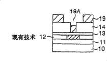
在双镶嵌工艺技术中有各种修改,图11A-11F表示采用双镶嵌工艺形成多层互连结构的典型常规方法。There are various modifications in the dual damascene process technology, and FIGS. 11A-11F illustrate a typical conventional method of forming a multi-level interconnection structure using the dual damascene process.
参见图11A,Si衬底10被CVD-SiO2膜等的层间绝缘膜11覆盖,并在层间绝缘膜11上形成互连图形12A。Si衬底10上承载各种半导体器件元件,如MOS晶体管(图中未示出)。Referring to FIG. 11A,
互连图形12A被埋置在形成在层间绝缘膜11上的相邻层间绝缘膜12B中以形成互连层12,其中互连层12被刻蚀停止膜13如SiN膜覆盖。刻蚀停止膜13还被相邻层间绝缘膜14覆盖。The
在图11A的步骤中,利用光刻工艺在层间绝缘膜14上形成光刻胶图形18,以使光刻胶图形18具有对应要形成的接触孔的开口18A,利用干刻蚀工艺同时采用光刻胶图形18作掩模,去掉层间绝缘膜14。作为干刻蚀工艺的结果,在层间绝缘膜14中形成对应要形成的接触孔的开口14A。In the step of FIG. 11A, a
接着,在图11B的步骤中,去掉光刻胶图形18并在图11C的步骤中在图11B的结构上形成光刻胶膜19,以便填充接触孔14A。通过利用光刻工艺构图如此形成的光刻胶膜19,在光刻胶膜19中形成对应要形成的互连图形的光刻胶开口19A。Next, in the step of FIG. 11B, the
然后,在图11D的步骤中,利用干刻蚀同时采用光刻胶膜19作掩模,构图在光刻胶开口19A上露出的层间绝缘膜14的露出部分。随后,去掉光刻胶膜19。作为这种构图工艺的结果,在层间绝缘膜14中形成除了接触孔14A之外对应所希望的互连凹槽的开口14B。Then, in the step of FIG. 11D, the exposed portion of the
接下来,在图11E的步骤中,通过利用RIE工艺的干刻蚀工艺去掉刻蚀停止膜13,并露出互连图形12A。Next, in the step of FIG. 11E, the
接着,在图11F的步骤中,用Al或Cu的导电膜填充互连凹槽14B和开口14A。通过对如此获得的结构施加化学机械抛光(CMP)工艺,获得通过接触孔14A与互连图形12A电连接的互连图形20。Next, in the step of FIG. 11F , the
通过重复前述工艺步骤,可以形成第三和第四互连图形。By repeating the aforementioned process steps, third and fourth interconnection patterns can be formed.
在用在半导体器件中的这种多层互连结构中,采用低介电性能绝缘膜用于层间绝缘膜12和14以便减少多层互连结构的杂散电容是非常重要的。通过减少杂散电容,提高了半导体器件的工作速度。因此已经做了很多尝试,采用低介电性能材料用于层间绝缘膜12或14,如掺杂F的SiO2膜(SiOF膜)、有机Si绝缘膜(SiOCH膜)等。特别是,通过采用有机Si绝缘膜,可以实现3.0或更小的比介电常数。In such a multilayer interconnect structure used in a semiconductor device, it is very important to use a low-dielectric insulating film for the
在利用双镶嵌工艺形成多层互连结构的这种工艺中,刻蚀停止膜13的作用非常重要,如前面注意到的。通常,呈现相对于层间绝缘膜14的大刻蚀选择性的SiN膜广泛地用于该目的。在双镶嵌工艺的技术中,刻蚀停止膜不仅必须具有大刻蚀选择性而且还用做阻挡构成互连图形的金属如Cu的有效阻挡层。此外,刻蚀停止膜必须具有相对于互连图形以及层间绝缘膜的优异粘接性。另外,刻蚀停止膜必须具有抵抗等离子体灰化工艺或湿刻蚀工艺的优异性能。都知道SiN膜用做有效的扩散阻挡层。In this process of forming a multilayer interconnection structure using the dual damascene process, the role of the
通常,很容易利用等离子体CVD工艺形成SiN膜。另一方面,如此形成的SiN膜具有7-8的大介电常数,因此采用SiN刻蚀停止膜13可基本上取消在多层互连结构中采用低介电性能绝缘膜作为层间绝缘膜12和14而实现的杂散电容减少的效果。In general, SiN films are easily formed using a plasma CVD process. On the other hand, the SiN film thus formed has a large dielectric constant of 7-8, so the use of the SiN
发明内容Contents of the invention
相应地,本发明的一般目的是提供一种新的可使用的半导体器件及其制造方法,其中消除了前述问题。Accordingly, it is a general object of the present invention to provide a new usable semiconductor device and method of manufacturing the same in which the aforementioned problems are eliminated.
本发明的另一和更特殊的目的是提供一种低介电性能氮化物膜及其制造方法。Another and more specific object of the present invention is to provide a low dielectric nitride film and a method for its manufacture.
本发明的又一目的是提供采用低介电性能氮化硅膜形成多层互连结构的方法。Another object of the present invention is to provide a method for forming a multilayer interconnection structure using a silicon nitride film with low dielectric properties.
本发明的再一目的是提供具有低介电性能氮化硅膜的半导体器件。Still another object of the present invention is to provide a semiconductor device having a silicon nitride film having low dielectric properties.
本发明的另一目的是提供形成氮化硅膜的方法,包括以下步骤:Another object of the present invention is to provide a method for forming a silicon nitride film, comprising the following steps:
在反应室中引入衬底;向所述处理室中引入其中具有有机硅氮烷键的有机Si化合物,作为气体源;向所述气体源输送能量;和利用CVD工艺,从所述气体源在所述衬底的表面上淀积含有Si、N、C和H作为基本构成元素的SiNCH膜,在向所述气体源输送能量时分配到所述气体源的气体分子的能量在所述硅氮烷键的结合能以下,所述SiNCH膜的比介电常数在3.5以上5.5以下。Introducing a substrate in a reaction chamber; introducing an organic Si compound having an organosilazane bond therein as a gas source into the processing chamber; delivering energy to the gas source; and using a CVD process, from the gas source at A SiNCH film containing Si, N, C, and H as basic constituent elements is deposited on the surface of the substrate, and when energy is delivered to the gas source, the energy of the gas molecules distributed to the gas source is in the silicon nitrogen The specific permittivity of the SiNCH film is not less than 3.5 and not more than 5.5 if the binding energy of the alkane bond is not greater than that.
根据本发明,通过采用其中含有有机硅氮烷键的有机Si化合物作为源料的CVD工艺,可以形成低密度SiNCH膜(含有Si、N、C和H作为基本或主要构成元素的膜)。如此形成的低密度SiNCH膜的特征在于低介电常数并具有相对于下层的优异粘接性。低密度SiNCH膜还用做阻挡金属原子如Cu的有效扩散阻挡层。低密度SiNCH膜呈现抵抗等离子体灰化工艺、干刻蚀或湿刻蚀工艺的优异性能。According to the present invention, a low-density SiNCH film (a film containing Si, N, C, and H as basic or main constituent elements) can be formed by a CVD process using an organic Si compound containing an organic silazane bond as a source material. The low-density SiNCH film thus formed is characterized by a low dielectric constant and has excellent adhesion to the underlying layer. The low density SiNCH film also acts as an effective diffusion barrier against metal atoms such as Cu. The low-density SiNCH film exhibits excellent performance against plasma ashing process, dry etching or wet etching process.
在本发明中,优选有机Si化合物具有(SiR1)nNR2、(SiR1NR2)n或(SiR1(NR2)1.5)n的结构式,其中n是1或更大的整数,R1和R2每个都可以是氢或选自烷基如甲基、环烃基如苯酚基或乙烯基的基。优选如此进行CVD工艺,以便Si化合物中的硅氮烷键基本上保持在SiNCH膜中。通过采用具有(SiR1)nNR2、(SiR1NR2)n或(SiR1(NR2)1.5)n结构式的化合物(R1和R2每个都可以是氢或选自烷基如甲基、环烃基如苯酚基或乙烯基的基,n是1或更大的整数),在CVD工艺期间源化合物中的有机硅氮烷键被保持在SiNCH膜中,并且SiNCH膜呈现减少的密度。In the present invention, it is preferable that the organic Si compound has a structural formula of (SiR1 )n NR2 , (SiR1 NR2 )n or (SiR1 (NR2 )1.5 )n , wherein n is an integer of 1 or more, RR andR can each be hydrogen or a group selected from alkyl such as methyl, cycloalkyl such as phenol or vinyl. The CVD process is preferably performed such that the silazane bond in the Si compound remains substantially in the SiNCH film. By employing a compound having the formula (SiR1 )n NR2 , (SiR1 NR2 )n or (SiR1 (NR2 )1.5 )n (R1 and R2 can each be hydrogen or be selected from alkyl such as methyl group, cyclic hydrocarbon group such as phenol group or vinyl group, n is an integer of 1 or more), the organosilazane bond in the source compound is maintained in the SiNCH film during the CVD process, and the SiNCH film exhibits reduced density.
优选,用于淀积SiNCH膜的CVD工艺包括有机Si化合物的等离子体聚合反应工艺。还优选等离子体聚合反应工艺是在有机Si化合物中的硅氮烷键基本上被保持在SiNCH膜中的等离子体功率下进行的。为此,有效地减小了SiNCH膜的比介电常数(specific dielectricconstant)。在通过有机Si化合物的热聚合反应工艺进行淀积SiNCH膜的步骤的情况下,必须设定温度,以使有机Si化合物中的有机硅氮烷键基本上被保持在淀积的SiNCH膜中。Preferably, the CVD process used to deposit the SiNCH film includes a plasma polymerization process of organic Si compounds. It is also preferred that the plasma polymerization process is performed under plasma power at which the silazane bonds in the organic Si compound are substantially maintained in the SiNCH film. For this reason, the specific dielectric constant (specific dielectric constant) of the SiNCH film is effectively reduced. In the case where the step of depositing the SiNCH film is performed by a thermal polymerization process of the organic Si compound, the temperature must be set so that the organosilazane bond in the organic Si compound is substantially maintained in the deposited SiNCH film.
在本发明中,可以通过替换工艺淀积SiNCH膜,在该工艺中,给前述有机Si化合物添加含有N的附加气体源如N2或NH3,形成附加气体源的等离子体,并给反应室输送等离子体。根据这种工艺,只给有机源化合物提供小等离子体功率,并有机Si化合物中的有机硅氮烷键保持在氮化硅膜中。In the present invention, the SiNCH film can be deposited by an alternative process in which an additional gas source containing N such asN2 orNH3 is added to the aforementioned organic Si compound, a plasma of the additional gas source is formed, and the reaction chamber Deliver plasma. According to this process, only a small plasma power is supplied to the organic source compound, and the organosilazane bond in the organic Si compound is maintained in the silicon nitride film.
在本发明中,还可以形成含有氧的SiONCH体系的硅氮氧化物膜,其中氧可以从源材料或附加源材料中释放出来。当膜中的氧含量为40%或更低时,硅氮氧化物膜呈现与前述氮化硅膜相似的性能。In the present invention, it is also possible to form a SiONCH system silicon oxynitride film containing oxygen in which oxygen can be released from a source material or an additional source material. When the oxygen content in the film is 40% or less, the silicon oxynitride film exhibits similar properties to the aforementioned silicon nitride film.
本发明的另一目的是提供制造半导体器件的方法,包括以下步骤:Another object of the present invention is to provide a method for manufacturing a semiconductor device, comprising the steps of:
在衬底上形成刻蚀停止膜;forming an etch stop film on the substrate;
在所述刻蚀停止膜上淀积层间绝缘膜;depositing an interlayer insulating film on the etch stop film;
构图所述层间绝缘膜以形成开口;patterning the interlayer insulating film to form openings;
刻蚀所述层间绝缘膜以在所述层间绝缘膜中形成对应所述开口的凹部;和etching the interlayer insulating film to form a recess corresponding to the opening in the interlayer insulating film; and
通过刻蚀工艺,选择地从所述开口刻蚀所述刻蚀停止膜,selectively etching the etch stop film from the opening by an etching process,
淀积所述刻蚀停止膜的所述步骤包括以下步骤:The step of depositing the etch stop film includes the following steps:
向处理装置的反应室中引入所述衬底;introducing the substrate into a reaction chamber of a processing device;
向所述反应室中输送其中含有有机硅氮烷键的有机Si化合物,作为气体源;和delivering an organoSi compound containing organosilazane bonds therein as a gas source into the reaction chamber; and
利用CVD工艺,在所述处理室中在所述衬底表面上由所述有机Si化合物淀积SiNCH膜,作为所述刻蚀停止膜。A SiNCH film is deposited from the organic Si compound on the surface of the substrate in the process chamber as the etch stop film by a CVD process.
根据本发明,在利用双镶嵌工艺形成多层互连结构时,利用CVD工艺由其中含有有机硅氮烷键的有机Si化合物的源材料形成的SiNCH膜用做氮化硅刻蚀停止膜。如此形成氮化硅膜中保持源材料中的有机硅氮烷键,其中有机硅氮烷键中包括烃基。因此,如此形成的氮化硅膜的特征在于低密度并具有低介电常数特性。通过采用这种低介电性能氮化硅膜作为刻蚀停止膜,基本上减少了多层互连结构的杂散电容,并相应地提高了半导体器件的工作速度。如此形成的低介电性能氮化硅膜具有优异耐刻蚀性的附加优点,因此低介电性能氮化硅膜可用做在双镶嵌工艺期间在干刻蚀工艺中的有效刻蚀停止膜或硬掩模。According to the present invention, a SiNCH film formed by a CVD process from a source material of an organic Si compound containing an organic silazane bond therein is used as a silicon nitride etch stop film when a multi-layer interconnection structure is formed by a dual damascene process. The organosilazane bond in the source material is thus formed in the silicon nitride film, wherein the organosilazane bond includes a hydrocarbon group. Therefore, the silicon nitride film thus formed is characterized by low density and has low dielectric constant characteristics. By using the silicon nitride film with low dielectric performance as the etching stop film, the stray capacitance of the multilayer interconnection structure is basically reduced, and the working speed of the semiconductor device is correspondingly improved. The low-dielectric silicon nitride film thus formed has the added advantage of excellent etch resistance, so the low-dielectric silicon nitride film can be used as an effective etch stop film or in a dry etching process during a dual damascene process. hard mask.
在本发明中,还优选有机Si化合物具有(SiR1)nNR2、(SiR1NR2)n或(SiR1(NR2)1.5)n的结构式,其中n是1或更大的整数,R1和R2每个都可以是氢或选自烷基如甲基、环烃基如苯酚基、或乙烯基的基。还优选进行CVD工艺,以便有机Si化合物中的硅氮烷键基本上保持在SiNCH膜中。通过采用具有(SiR1)nNR2、(SiR1NR2)n或(SiR1(NR2)1.5)n结构式的化合物,(R1和R2是氢或选自烷基如甲基、环烃基如苯酚基、或乙烯基的基,n是1或更大的整数),在CVD工艺期间源化合物中的有机硅氮烷键可以保持在SiNCH膜中,并且SiNCH膜呈现减小的密度。In the present invention, it is also preferable that the organic Si compound has a structural formula of (SiR1 )n NR2 , (SiR1 NR2 )n or (SiR1 (NR2 )1.5 )n , wherein n is an integer of 1 or more, Eachof R andR can be hydrogen or a group selected from alkyl such as methyl, cycloalkyl such as phenol, or vinyl. It is also preferable to perform the CVD process so that the silazane bond in the organic Si compound remains substantially in the SiNCH film. By using a compound having the formula (SiR1 )n NR2 , (SiR1 NR2 )n or (SiR1 (NR2 )1.5 )n , (R1 and R2 are hydrogen or are selected from alkyl such as methyl, Cyclohydrocarbon group such as phenol group, or vinyl group, n is 1 or greater integer), the organic silazane bond in the source compound can be kept in the SiNCH film during the CVD process, and the SiNCH film exhibits a reduced density .
优选,用于淀积SiNCH膜的CVD工艺包括有机Si化合物的等离子体聚合反应工艺。还优选在其中有机Si化合物中的有机硅氮烷键基本上保持在SiNCH膜中的等离子体功率下进行等离子体聚合反应工艺。因此,有效地减小了SiNCH膜的密度和比介电常数。在通过有机Si化合物的热聚合反应工艺进行淀积SiNCH膜的步骤的情况下,需要设定温度,以使有机Si化合物中的有机硅氮烷键基本上保持在被淀积的SiNCH膜中。Preferably, the CVD process used to deposit the SiNCH film includes a plasma polymerization process of organic Si compounds. It is also preferable to perform the plasma polymerization process under plasma power in which the organosilazane bond in the organic Si compound is substantially maintained in the SiNCH film. Therefore, the density and specific permittivity of the SiNCH film are effectively reduced. In the case where the step of depositing the SiNCH film is performed by the thermal polymerization process of the organic Si compound, it is necessary to set the temperature so that the organosilazane bond in the organic Si compound is substantially maintained in the deposited SiNCH film.
在本发明中,还可以通过以下替换工艺淀积SiNCH膜:给前述有机Si化合物添加含有N的附加气体源如N2或NH3,形成附加气体源的等离子体,并且该将等离子体输送给反应室。根据这个工艺,只需要给有机源化合物提供小等离子体功率,并且有机Si化合物中的有机硅氮烷结构保持在氮化硅膜中。In the present invention, the SiNCH film can also be deposited by the following alternative process: adding an additional gas source containing N such as N2 or NH3 to the aforementioned organic Si compound, forming a plasma of the additional gas source, and feeding the plasma to reaction chamber. According to this process, only a small plasma power needs to be supplied to the organic source compound, and the organosilazane structure in the organic Si compound is maintained in the silicon nitride film.
在本发明中,还可以施加在层间绝缘膜上淀积导体层的工艺,以便经过开口填充凹部,并利用化学机械抛光工艺去掉位于层间绝缘膜上面的部分导体层。因此,优选导体层由Cu形成。由于氮化硅膜用做抵抗Cu的有效扩散阻挡层,因此这种结构可以有效地抑制Cu从Cu层扩散到相邻层间绝缘膜。此外,如此形成的氮化硅刻蚀停止膜具有优异的泄漏特性。In the present invention, it is also possible to apply a process of depositing a conductor layer on the interlayer insulating film to fill the recess through the opening, and remove part of the conductor layer on the interlayer insulating film by chemical mechanical polishing. Therefore, it is preferable that the conductor layer is formed of Cu. Since the silicon nitride film acts as an effective diffusion barrier against Cu, this structure can effectively suppress the diffusion of Cu from the Cu layer to the adjacent interlayer insulating film. In addition, the silicon nitride etch stop film thus formed has excellent leakage characteristics.
通过采用有机绝缘膜或掺杂F的SiO2膜作为层间绝缘膜,减小了层间绝缘膜的电容并减少了多层互连结构的总杂散电容。通过形成前述凹部以便包括互连凹槽或接触孔,可以形成各种复杂的互连图形。By adopting an organic insulating film or an F-dopedSiO2 film as an interlayer insulating film, the capacitance of the interlayer insulating film is reduced and the total stray capacitance of the multilayer interconnection structure is reduced. By forming the foregoing recesses so as to include interconnection grooves or contact holes, various complicated interconnection patterns can be formed.
本发明的另一目的是提供SiNCH体系的氮化硅膜,所述氮化硅膜中含有表示为CnHm的任意原子集团,所述原子集团与Si原子键合,其中n是1以上的整数,m是比0大的整数。Another object of the present invention is to provide a silicon nitride film of the SiNCH system, which contains any atomic group represented by Cn Hm bonded to Si atoms, wherein n is 1 or more Integer, m is an integer greater than 0.
根据本发明,氮化硅膜中含有有机硅氮烷键,而有机硅氮烷键中又含有烃基。本发明的氮化硅膜具有低膜密度特性和低介电常数的相关特性。该原子集团可以是烷基、环烃基或乙烯基的任何一个。本发明的氮化硅膜具有优异粘接性和抵抗各种工艺如等离子体灰化工艺、干刻蚀工艺或湿刻蚀工艺的特性的有利特征。该氮化硅膜还用做有效扩散阻挡层并且其特征在于小漏电流。According to the present invention, the silicon nitride film contains organosilazane bonds, and the organosilazane bonds contain hydrocarbon groups. The silicon nitride film of the present invention has low film density characteristics and related characteristics of low dielectric constant. The atomic group may be any one of an alkyl group, a cyclohydrocarbyl group or a vinyl group. The silicon nitride film of the present invention has advantageous features of excellent adhesion and resistance to various processes such as plasma ashing process, dry etching process or wet etching process. The silicon nitride film also acts as an effective diffusion barrier and is characterized by a small leakage current.
本发明的再一目的是提供半导体器件,包括:Another object of the present invention is to provide a semiconductor device, comprising:
衬底;和形成在所述衬底上的多层互连结构,a substrate; and a multilayer interconnect structure formed on said substrate,
所述多层互连结构包括刻蚀停止膜、形成在所述刻蚀停止膜上的层间绝缘膜、形成在所述层间绝缘膜中的互连凹槽、形成在所述层间绝缘膜中并对应所述互连凹槽的接触孔、和填充所述互连凹槽和所述接触孔的导体层,其中所述刻蚀停止膜包括SiNCH膜并且其中含有表示为CnHm的任意原子集团,所述原子集团与Si原子键合。The multilayer interconnection structure includes an etching stopper film, an interlayer insulating film formed on the etching stopper film, an interconnection groove formed in the interlayer insulating film, an interlayer insulating film formed on the interlayer insulating A contact hole in the film and corresponding to the interconnection groove, and a conductor layer filling the interconnection groove and the contact hole, wherein the etch stop film comprises a SiNCH film and contains a compound denoted as Cn Hm An arbitrary atomic group of , which is bonded to a Si atom.
根据本发明,氮化硅膜中含有有机硅氮烷键,而有机硅氮烷键中又含有烃基。结果是,减小了氮化硅膜的密度并相应减小了介电常数。因此,减小了多层互连结构的杂散电容并提高了半导体器件的工作速度。对于原子集团,可采用氢、烷基、环烃基、或乙烯基的任何一种。本发明的氮化硅膜呈现优异的粘接性和抵抗等离子体灰化工艺、干刻蚀工艺或湿刻蚀工艺的特性。此外,本发明的氮化硅膜用做阻止金属元素扩散的有效扩散阻挡层。另外,本发明的氮化硅膜具有减小的漏电流的有利特征。According to the present invention, the silicon nitride film contains organosilazane bonds, and the organosilazane bonds contain hydrocarbon groups. As a result, the density of the silicon nitride film is reduced and the dielectric constant is reduced accordingly. Therefore, the stray capacitance of the multilayer interconnect structure is reduced and the operating speed of the semiconductor device is increased. As the atomic group, any of hydrogen, alkyl, cyclohydrocarbyl, or vinyl can be used. The silicon nitride film of the present invention exhibits excellent adhesion and resistance to plasma ashing process, dry etching process or wet etching process. In addition, the silicon nitride film of the present invention serves as an effective diffusion barrier against the diffusion of metal elements. In addition, the silicon nitride film of the present invention has an advantageous feature of reduced leakage current.
在结合附图阅读了下面的详细说明之后将使本发明的其它目的和附加特点更显然。Other objects and additional features of the present invention will become apparent after reading the following detailed description in conjunction with the accompanying drawings.
附图说明Description of drawings
图1是表示用在本发明第一实施例中的等离子体CVD装置的结构的示意图;FIG. 1 is a schematic diagram showing the structure of a plasma CVD apparatus used in a first embodiment of the present invention;
图2A和2B是表示用在本发明第一实施例中的有机硅氮烷键的例子的示意图;2A and 2B are schematic diagrams showing examples of organosilazane bonds used in the first embodiment of the present invention;
图3A和3B是表示在本发明第一实施例中获得的氮化硅膜结构的例子的示意图;3A and 3B are schematic views showing an example of the structure of a silicon nitride film obtained in the first embodiment of the present invention;
图4A-4F是表示根据本发明第二实施例的半导体器件的制造工艺的示意图;4A-4F are schematic diagrams showing a manufacturing process of a semiconductor device according to a second embodiment of the present invention;
图5A-5E是表示根据本发明第三实施例的半导体器件的制造工艺的示意图;5A-5E are schematic diagrams showing a manufacturing process of a semiconductor device according to a third embodiment of the present invention;
图6A-6E是表示根据本发明第四实施例的半导体器件的制造工艺的示意图;6A-6E are schematic diagrams showing a manufacturing process of a semiconductor device according to a fourth embodiment of the present invention;
图7A-7E是表示根据本发明第五实施例的半导体器件的制造工艺的示意图;7A-7E are schematic diagrams showing a manufacturing process of a semiconductor device according to a fifth embodiment of the present invention;
图8A-8E是表示根据本发明第六实施例的半导体器件的制造工艺的示意图;8A-8E are schematic diagrams showing a manufacturing process of a semiconductor device according to a sixth embodiment of the present invention;
图9是表示根据本发明第七实施例的半导体器件的结构的示意图;9 is a schematic diagram showing the structure of a semiconductor device according to a seventh embodiment of the present invention;
图10是表示第七实施例的半导体器件的制造工艺的示意图;10 is a schematic view showing a manufacturing process of the semiconductor device of the seventh embodiment;
图11A-11F是表示常规半导体器件的制造工艺的示意图。11A-11F are schematic diagrams showing a manufacturing process of a conventional semiconductor device.
具体实施方式Detailed ways
(第一实施例)(first embodiment)
图1表示用在本发明第一实施例中的等离子体CVD装置30的结构。Fig. 1 shows the structure of a
参见图1,等离子体CVD装置30包括由泵31C经过排气口31A和收集器(trap)31B抽真空的反应室31,其中反应室31中安装用于固定待处理衬底32A的工作台32。1, the
在处理室31中,提供面对工作台32的簇射头(showerhead)33,其中从容器34给簇射头33输送液态有机Si源。更具体地说,容器34被He气体加压,并且其中的液态有机Si源作为第一气体源经过液体质量流控制器34A和喷雾器34B并与从管道34C输送的Ar载体气体一起输送给簇射头33。In the
此外,经过管道35给簇射头33输送作为第二气体源的NH3气体或N2气体,并且通过从射频电源36给其输送450KHz-60MHz的射频功率,在第一和第二气体源中进行等离子体激发。In addition,NH3 gas orN2 gas as the second gas source is delivered to the
通过形成等离子体,随着从簇射头33释放源材料,在反应室31中进行等离子体聚合反应,并且如此输送的源材料进行等离子体激发。作为等离子体激发的结果,在衬底32A的表面上淀积氮化硅膜。By forming plasma, as the source material is released from the
在图1的结构中,应该注意到泵31C连接到洗涤器单元31D,泵31C的废气被洗涤器单元31D处理之后释放到环境中。In the configuration of Figure 1, it should be noted that the
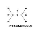
图2A和2B表示保持在源容器34中的示意有机Si源材料的结构式,其中图2A表示其中1,1,3,3,5,5,7,7-辛甲基环四硅氮烷(octamethylcyclotetrasilazane)用做有机Si源的情况。在图2A中,R1是甲基,R2是氢。因此,有机Si源具有Si4C8H28N4的结构式。另一方面,在图2B的例子中,六甲基二硅氮烷(Si2C6H19N)用做有机Si源。应该注意这些只是含有有机硅氮烷键的有机Si源的示意例子,硅氮烷键是用于其中含有Si-N-Si键的化合物一般术语。硅氮烷键是通过给Si-N-Si键添加烷基如甲基或乙基、或环烃基如苯基、或乙烯基获得的。2A and 2B represent the structural formula of the schematic organic Si source material held in the
有机硅氮烷化合物的例子概括示于下列表I中。Examples of organosilazane compounds are summarized in Table I below.
表ITable I
参见图2A和2B,前述有机Si源含有具有甲基Me的有机硅氮烷键并具有由通式(SiR1)nR2或(SiR1NR2)n表示的成分,其中n是1或更大的整数,而R1和R2具有CmH2m+1(m是大于零的整数)的通式,并且可以是氢原子、烷基、环烃基如苯基或乙烯基的任何一种。2A and 2B, the aforementioned organic Si source contains an organosilazane bond having a methyl group Me and has a composition represented by the general formula (SiR1 )n R2 or (SiR1 NR2 )n , where n is 1 or Larger integers, and R1 and R2 have the general formula of Cm H2m+1 (m is an integer greater than zero), and can be any of a hydrogen atom, an alkyl group, a cyclic hydrocarbon group such as a phenyl group or a vinyl group.
采用上述有机Si源作为源,在图1的CVD设备30中同时采用Si晶片做衬底32A在8英寸Si晶片上淀积氮化硅膜。氮化硅膜的淀积是在200-400℃的衬底温度下同时以27MHz的频率输送100-1000W的等离子体功率进行的。详细的条件概括列于表II中。Using the above-mentioned organic Si source as a source, a silicon nitride film was deposited on an 8-inch Si wafer in the
表IITable II
如此获得的氮化硅膜实际上是SiNCH膜并具有3.5-5.5的比介电常数。The silicon nitride film thus obtained is actually a SiNCH film and has a specific permittivity of 3.5-5.5.
应该注意到,鉴于普通等离子体SiN膜具有约7-8的比介电常数,该氮化硅膜的比介电常数的值已经下降到一半。通过在前述淀积工艺中利用100-300W的小等离子体功率,从簇射头33输送的汽化的有机Si化合物在反应室31中不完全分解,并且有机源中的有机硅氮烷键基本上保持在如此淀积在Si晶片上的氮化硅膜中。由于有机硅氮烷键的存在导致淀积的SiN膜的密度下降,还引起淀积的SiN膜的比介电常数减小。It should be noted that the value of the specific permittivity of this silicon nitride film has dropped to half, whereas ordinary plasma SiN films have a specific permittivity of about 7-8. By using a small plasma power of 100-300W in the aforementioned deposition process, the vaporized organic Si compound delivered from the
图3A示出了利用FT-IR法观察到的如此形成的氮化硅膜的结构。FIG. 3A shows the structure of the silicon nitride film thus formed observed by the FT-IR method.
参见图3A,可以看到如此形成的氮化硅膜中保持从图2A和2B的有机硅氮烷键得到的Si-CH3或CH3的烃结构,而氮化硅膜中的烃结构减小了密度,由此减小了氮化硅膜的比介电常数。Referring to FIG. 3A, it can be seen that the Si-CH orCH hydrocarbon structure obtained from the organic silazane bonds in FIGS. The density is reduced, thereby reducing the specific dielectric constant of the silicon nitride film.
图3A还示出了在与采用1000W的等离子体功率相比采用100W的等离子体功率时,对应Si-CH3键的峰值的相对高度相对于对应SiN键的峰值而增加。这个结果清楚地显示了与利用1000W等离子体功率形成的氮化硅膜相比利用100W的等离子体功率形成的氮化硅膜含有增加浓度的Si-CH3键。因此,推断出比介电常数的所希望的减小是由于淀积的氮化硅膜中的膜密度的减小造成的。FIG. 3A also shows that the relative height of the peaks corresponding to Si—CH3 bonds increases relative to the peaks corresponding to SiN bonds when using a plasma power of 100 W compared to using a plasma power of 1000 W. This result clearly shows that the silicon nitride film formed with a plasma power of 100 W contains an increased concentration of Si—CH3 bonds compared to the silicon nitride film formed with a plasma power of 1000 W. Therefore, it is deduced that the desired decrease in specific permittivity is due to the decrease in film density in the deposited silicon nitride film.
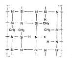
图3B显示了如此形成的氮化硅膜的示意结构。Fig. 3B shows a schematic structure of the silicon nitride film thus formed.
参见图3B,该氮化硅膜除了常用的Si-N结构之外还包括一起形成网络结构的Si-CH3键、N-H键、Si-H键等。具有这种网络结构的氮化硅膜可以由有机硅氮烷键源同时适当选择例如等离子体功率等条件而形成。Referring to FIG. 3B , the silicon nitride film includes Si—CH3 bonds, NH bonds, Si—H bonds, etc. that together form a network structure in addition to the commonly used Si—N structure. A silicon nitride film having such a network structure can be formed from an organosilazane bond source while appropriately selecting conditions such as plasma power.
应该注意到如此获得的SiNCH膜呈现相对于下层膜的优异粘接性。此外,SiNCH膜呈现抵抗等离子体灰化、干刻蚀和湿刻蚀的优异特性。因此,本发明的SiNCH膜可以成功地用在多层互连结构中。It should be noted that the SiNCH film thus obtained exhibits excellent adhesion to the underlying film. In addition, SiNCH films exhibit excellent properties against plasma ashing, dry etching, and wet etching. Therefore, the SiNCH film of the present invention can be successfully used in multilayer interconnect structures.
应该注意到表II中只是示出了典型例子,还可以通过在50-2000W范围内调整等离子体功率、在从室温到500℃的范围内调整衬底温度、在1.33-1.33kPa(10毫乇-10乇)范围内调整处理压力、或在0.001-10cc/min范围内调整液态有机Si源的输送速度来形成本发明的SiNCH膜。It should be noted that only typical examples are shown in Table II, and the plasma power can also be adjusted in the range of 50-2000W, the substrate temperature can be adjusted in the range from room temperature to 500°C, and the temperature can be adjusted at 1.33-1.33kPa (10 The SiNCH film of the present invention can be formed by adjusting the processing pressure within the range of -10 Torr), or adjusting the delivery speed of the liquid organic Si source within the range of 0.001-10cc/min.
此外,还可以通过热解CVD工艺形成SiNCH膜。例如,这种热解CVD工艺可以在图2的等离子体CVD设备30中进行而不用激发射频电源36。In addition, a SiNCH film can also be formed by a pyrolytic CVD process. For example, such a pyrolytic CVD process can be performed in
在这种情况下,衬底温度设定得比在等离子体CVD工艺中采用的衬底温度高。然而,衬底温度应该不超过600℃。否则,包含在有机Si源中的有机硅氮烷键不会保持在SiNCH膜中。In this case, the substrate temperature is set higher than that used in the plasma CVD process. However, the substrate temperature should not exceed 600°C. Otherwise, the organosilazane bonds contained in the organic Si source would not remain in the SiNCH film.
[第二实施例][Second embodiment]
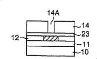
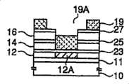
图4A-4F表示根据本发明第二实施例的具有多层互连结构的半导体器件的制造工艺,其中对应前述部件的那些部件利用相同的参考标记表示并省略其说明。4A-4F show a manufacturing process of a semiconductor device having a multilayer interconnection structure according to a second embodiment of the present invention, wherein those components corresponding to the aforementioned components are denoted by the same reference numerals and their descriptions are omitted.
图4A对应前述图11A的步骤,并且形成相同的叠层结构,除了在表II条件下利用图2的等离子体CVD设备由图2A的有机Si源形成的SiNCH膜代替刻蚀停止膜13用于刻蚀停止膜之外。FIG. 4A corresponds to the aforementioned step of FIG. 11A, and the same stacked structure is formed, except that the SiNCH film formed from the organic Si source of FIG. 2A is used in place of the
在图4B的步骤中,采用光刻胶图形18作掩模,对层间绝缘膜14进行干刻蚀,并在层间绝缘膜14中形成对应光刻胶开口18A的开口。形成开口之后,去掉光刻胶图形18。In the step of FIG. 4B , the
接着,在图4C的步骤中,重新在图4B的结构上形成光刻胶膜19,其中然后利用光刻构图工艺对光刻胶膜19进行构图以形成光刻胶开口19A,其对应要在多层互连结构中形成的互连图形。Next, in the step of FIG. 4C, a
接着,在图4D的步骤中,采用光刻胶膜19做掩模的同时,在由光刻胶开口19A露出的部分中利用干刻蚀工艺刻蚀掉层间绝缘膜14,之后去掉光刻胶膜19本身。作为前述干刻蚀工艺和光刻胶去除工艺的结果,在开口14A的底部露出SiNCH膜23。Next, in the step of FIG. 4D, while using the
随后,在图4E的步骤中,对如此获得的结构进行干刻蚀工艺,并在SiNCH膜23中对应开口14A形成开口14B。Subsequently, in the step of FIG. 4E , the structure thus obtained is subjected to a dry etching process, and an
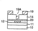
此外,在图4F的步骤中,利用Ta、TaN、Ta/TaN、TiN、WN等的阻挡金属层(未示出)覆盖由开口14B形成的互连凹槽和由开口14A形成接触孔,然后用导体层如Cu层填充。通过利用CMP工艺去除覆盖层间绝缘膜14的导体层,获得在接触孔14A与下层互连图形14B接触的导体图形20,如图4F所示。In addition, in the step of FIG. 4F, the interconnect groove formed by the opening 14B and the contact hole formed by the
对于层间绝缘膜14,可以采用无机低介电性能绝缘膜,如掺杂F的SiO2膜、HSQ膜如SiOH膜或多孔绝缘膜。或者,可以采用低介电性能有机绝缘膜如有机SOG膜或芳香族低介电性能有机绝缘膜用于层间绝缘膜14。当然,可以采用常规CVD-SiO2膜或SOG膜用于层间绝缘膜14。通过采用低介电性能无机或有机绝缘膜用于多层互连结构中的层间绝缘膜14,可以减小多层互连结构的总介电常数并提高半导体器件的工作速度。For the
应该注意到本例的SiNCH膜23具有各种特性,如优异的粘接性、优异的抗干刻蚀性、作为阻挡Cu的扩散阻挡层的优异性能、低漏电流等,适合用在高速半导体器件的多层互连结构中。It should be noted that the
[第三实施例][Third embodiment]
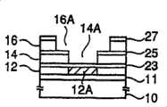
图5A-5E是表示根据本发明第三实施例的半导体器件的制造工艺的示意图,其中对应前述部件的那些部件用相同的参考标记表示,并省略其说明。5A-5E are schematic diagrams showing a manufacturing process of a semiconductor device according to a third embodiment of the present invention, wherein those components corresponding to the aforementioned components are denoted by the same reference numerals, and descriptions thereof are omitted.
参见图5A,该步骤基本上与前述图4A的步骤相同,除了还提供层间绝缘膜16和SiNCH膜25和27之外。Referring to FIG. 5A, this step is basically the same as the aforementioned step of FIG. 4A except that an
更具体地说,图5A的叠层结构除了形成在Si衬底10层上的间绝缘膜11和形成在层间绝缘膜11上的互连层12之外还包括SiNCH膜23、层间绝缘膜14、SiNCH膜25、层间绝缘膜16和SiNCH膜27,以便膜23-27连续堆叠在一起,并且在如此形成的叠层结构上提供具有光刻胶开口18A的光刻胶图形。与前述实施例相同,光刻胶开口18A要形成在多层互连结构中的对应接触孔。More specifically, the laminated structure of FIG. 5A includes, in addition to the
接着,在图5B的步骤中,采用光刻胶图形18作掩模,对SiNCH膜27进行干刻蚀工艺,并在其中对应光刻胶开口18A形成开口(未示出)。Next, in the step of FIG. 5B , using the
如此形成的开口露出下层层间绝缘膜16的一部分,并且对层间绝缘膜16的露出部分进行干刻蚀工艺。结果是,在层间绝缘膜16中对应光刻胶开口18A形成开口,以便露出一部分下层SiNCH膜25。通过对如此形成的SiNCH膜25进行干刻蚀工艺,对应光刻胶开口18A形成露出下层层间绝缘膜14的开口。The opening thus formed exposes a portion of the underlying
此外,通过对如此露出的层间绝缘膜14进行干刻蚀工艺,在层间绝缘膜14中对应光刻胶开口18A形成开口14A。如此形成的开口14A连续通过SiNCH膜27、层间绝缘膜16、SiNCH膜25和层间绝缘膜14延伸,并在其底部露出SiNCH膜23。Further, by performing a dry etching process on the
接下来,在图5C的步骤中,除去光刻胶膜18,并利用旋涂工艺在图5B的结构上形成另一光刻胶膜19,以便光刻胶膜19填充开口14A,并且在图5D的步骤中对光刻胶膜19进行光刻构图工艺。结果是,在光刻胶膜19中形成光刻胶开口19A,其对应要形成在多层互连结构中的互连凹槽。Next, in the step of FIG. 5C, the
接着,在图5E的步骤中,采用光刻胶膜19作掩模,在由光刻胶开口19A露出的部分中对SiNCH膜27进行干刻蚀工艺,在SiNCH膜27中对应光刻胶开口19A形成开口,以便该开口露出下层层间绝缘膜16中。然后对如此露出的层间绝缘膜16进行干刻蚀工艺,直到露出下层SiNCH膜25为止。结果是,在层间绝缘膜16中形成开口16A,其对应要在多层互连结构中对应光刻胶开口19A形成的互连凹槽。之后,除去光刻胶开口19A。Next, in the step of FIG. 5E , the
应该注意到用于形成开口18A的干刻蚀工艺由于露出SiNCH膜25而停止。然后通过除去露出的SiNCH膜27、25和23并用导体层如Cu层填充开口16A和14A,获得前面参照图4F说明的多层互连结构。It should be noted that the dry etching process for forming the
在本例中,还可以采用任何低介电性能无机绝缘膜如掺杂F的SiO2膜、HSQ膜如SiOH膜或多孔膜,或者低介电性能有机绝缘膜,如有机SOG膜或芳香族有机绝缘膜用于层间绝缘膜14和16。在本例的多层互连结构中,总介电常数减少了,并提高了半导体器件的工作速度。In this example, any low-dielectric inorganic insulating film such as F-doped SiO2 film, HSQ film such as SiOH film or porous film, or low-dielectric organic insulating film such as organic SOG film or aromatic organic film can also be used. An insulating film is used for the interlayer insulating
在本例中,SiNCH膜23、25和27的特征在于低的比介电常数、优异粘接性、优异抗干刻蚀特性、作为Cu的扩散阻挡层的优异性能、和低漏电流。因此,本发明的SiNCH膜用在高速半导体器件的多层互连结构中是很理想的。In this example,
[第四实施例][Fourth embodiment]
图6A-6E表示根据本发明第四实施例的半导体器件的制造工艺,其中对应前述部件的那些部件用相同的参考标记表示并省略其说明。6A-6E show a manufacturing process of a semiconductor device according to a fourth embodiment of the present invention, in which those components corresponding to the aforementioned components are denoted by the same reference numerals and their descriptions are omitted.
参见图6A,该步骤基本上与图5A的步骤相同,并在Si衬底10上形成层叠体,其中利用其上承载互连图形12的层间绝缘膜11覆盖Si衬底10。此外,SiNCH膜23、层间绝缘膜14、SiNCH膜25、层间绝缘膜16和SiNCH膜27连续堆叠在互连层12上。在本例中,在多层互连结构上提供光刻胶图形28,其中光刻胶图形28包括光刻胶开口28A,其对应要形成在多层互连结构中的互连图形。Referring to FIG. 6A, this step is basically the same as that of FIG. 5A, and a laminated body is formed on a
在图6B的步骤中,采用光刻胶图形28作掩模,对SiNCH膜27进行干刻蚀工艺,在SiNCH膜27中对应光刻胶开口28A形成开口,以便如此形成的开口暴露出在SiNCH膜27下面形成的层间绝缘膜16。对如此露出的层间绝缘膜16进行干刻蚀工艺,并在对应光刻胶开口28A的层间绝缘膜16中形成对应要形成的互连凹槽的开口16A,以便露出下层SiNCH膜25。In the step of FIG. 6B, the
接着,在图6C的步骤中除去光刻胶膜28,并在图6B的结构上重新形成光刻胶膜29,以便光刻胶膜29填充开口16A。此外,在图6D的步骤中利用光刻工艺对光刻胶膜29构图,以便在光刻胶膜29中形成光刻胶开口29A,其对应要形成在多层互连结构中的接触孔。Next, the
接下来,在图6E的步骤中,采用光刻胶图形29作掩模,对由光刻胶开口29A露出的一部分SiNCH膜25进行干刻蚀工艺,并在SiNCH膜25中对应光刻胶开口29A形成开口,以便露出下层层间绝缘膜14。之后,除去光刻胶图形29,并采用SiNCH膜27和25作硬掩模对层间绝缘膜14进行干刻蚀工艺。结果是,在层间绝缘膜14中对应光刻胶开口29A形成开口14A,并对应要形成在多层互连结构中的接触孔。Next, in the step of FIG. 6E, the
用于形成开口14A的干刻蚀工艺由于露出SiNCH膜23而停止。之后,除去露出的SiNCH膜27、25和23,并用导体层如Cu层填充开口16A和14A。结果是,获得参照图6F说明的多层互连结构。The dry etching process for forming the
在本例中,还可以采用任何无机低介电性能绝缘膜如掺杂F的SiO2膜、HSQ膜如SiOH膜或多孔膜,或者有机低介电性能绝缘膜,如有机SOG膜或芳香族有机绝缘膜。结果是,本例的多层互连结构具有总介电常数减少了和半导体器件的工作速度基本上提高了的优点。In this example, any inorganic low-dielectric insulating film such as F-dopedSiO2 film, HSQ film such as SiOH film or porous film, or organic low-dielectric insulating film such as organic SOG film or aromatic organic insulating film. As a result, the multilayer interconnection structure of this example has the advantages of a reduction in the overall dielectric constant and a substantial increase in the operating speed of the semiconductor device.
在本例中,SiNCH膜23、25和27的特征在于低的比介电常数、优异粘接性、优异抗干刻蚀特性、作为Cu的扩散阻挡层的优异性能和低漏电流。因此,本发明的SiNCH膜用在高速半导体器件的多层互连结构中是很理想的。In this example, the
[第五实施例][Fifth Embodiment]
图7A-7E表示根据本发明第五实施例的半导体器件的制造工艺,其中对应前述部件的那些部件用相同的参考标记表示并省略其说明。7A-7E show a manufacturing process of a semiconductor device according to a fifth embodiment of the present invention, in which components corresponding to the aforementioned components are denoted by the same reference numerals and description thereof is omitted.
参见图7A,与前述实施例相同,在Si衬底10上形成叠层结构,其中Si衬底10上承载层间绝缘膜11,层间绝缘膜12上承载互连层12。在互连层12上,连续堆叠SiNCH膜23、层间绝缘膜14和SiNCH膜25,其中SiNCH膜25上承载光刻胶图形41,该光刻胶图形具有对应要形成在多层互连结构中的接触孔的光刻胶开口41A。Referring to FIG. 7A , similar to the previous embodiments, a stacked structure is formed on a
光刻胶开口41A露出SiNCH膜25,因此对SiNCH膜25进行干刻蚀工艺。结果是,在SiNCH膜25中对应光刻胶开口41A形成开口25A。The
接着,在图7B的步骤中,在SiNCH膜25上淀积层间绝缘膜16,以便填充开口25A,接着在层间绝缘膜16上淀积SiNCH膜27。Next, in the step of FIG. 7B ,
然后,在图7C的步骤中,在SiNCH膜27上施加光刻胶膜42,其中利用光刻工艺在图7D的步骤中对光刻胶膜42进行构图,以便在光刻胶膜42中对应要形成在多层互连结构中的互连图形形成开口42A。Then, in the step of FIG. 7C, a
接下来,在图7E的步骤中,采用光刻胶膜42作掩模,对在开口42A露出的SiNCH膜27的露出部分进行干刻蚀工艺,直到露出下层层间绝缘膜16为止。Next, in the step of FIG. 7E , using the
接着,对层间绝缘膜16进行干刻蚀工艺,并且在层间绝缘膜16中对应前述光刻胶开口42A形成开口16A,其还对应要形成的互连凹槽。应该注意层间绝缘膜16的干刻蚀工艺由于在其中形成SiNCH膜25的部分中露出SiNCH膜25而停止,而在其中在膜25中形成开口25A的部分中,干刻蚀工艺通过开口25A进行到下层层间绝缘膜14内部,并在层间绝缘膜14中对应前述开口25A并因此对应要形成在多层互连结构中的接触孔形成开口14A。Next, a dry etching process is performed on the
用于形成开口14A的干刻蚀工艺由于露出SiNCH膜23而停止。随后,除去露出的SiNCH膜27、25和23并用Cu等的导体层填充开口16A和14A。结果是,获得参照图4F说明的多层互连结构。The dry etching process for forming the
在本例中,还可以采用任何无机低介电性能绝缘膜如掺杂F的SiO2膜、HSQ膜如SiOH膜或多孔膜,或者有机低介电性能绝缘膜,如有机SOG膜或芳香族有机绝缘膜用于层间绝缘膜14和16。由此,减小了该多层互连结构的总介电常数并提高了半导体器件的工作速度。In this example, any inorganic low-dielectric insulating film such as F-dopedSiO2 film, HSQ film such as SiOH film or porous film, or organic low-dielectric insulating film such as organic SOG film or aromatic An organic insulating film is used for the interlayer insulating
在本例中,SiNCH膜23、25和27具有各种优选的特性,如低的比介电常数、优异粘接性、优异抗干刻蚀特性、作为Cu的扩散阻挡层的优异性能和低漏电流,因此,本发明的SiNCH膜用在高速半导体器件的多层互连结构中是很理想的。In this example, the
[第六实施例][Sixth embodiment]
图8A-8E是表示根据本发明第六实施例的具有多层互连结构的半导体器件的制造工艺的示意图,该制造工艺采用了所谓的成组硬掩模,其中对应前述部件的那些部件用相同的参考标记表示并省略其说明。8A-8E are schematic diagrams showing a manufacturing process of a semiconductor device having a multilayer interconnection structure according to a sixth embodiment of the present invention, the manufacturing process employing a so-called ganged hard mask, wherein those corresponding to the aforementioned components are used The same reference numerals are indicated and descriptions thereof are omitted.
在本例中,依次堆叠SiNCH膜23、层间绝缘膜14、SiNCH膜25、层间绝缘膜16和SiNCH膜27,与前述实施例一样。此外,利用等离子体CVD工艺或旋涂工艺在SiNCH膜27上形成SiO2膜43,用包括对应要形成在多层互连结构中的接触孔的光刻胶开口18A的光刻胶膜18覆盖如此形成的SiO2膜43。SiNCH膜27和SiO2膜43一起形成成组掩模。In this example, the
在图8A的步骤中,采用光刻胶膜18作掩模,对SiO2膜进行干刻蚀工艺,并在SiO2膜43中对应光刻胶开口18A形成开口,以便露出位于SiO2膜43下面的SiNCH膜27。此外,对如此露出的SiNCH膜27进行干刻蚀工艺,并在SiNCH膜27中对应光刻胶开口18A形成开口27A,以便露出层间绝缘膜16,如图8B所示。In the step of FIG. 8A, the
在图8B的步骤中,在SiO2膜43上形成具有对应要形成在多层互连结构中的互连凹槽的光刻胶开口19A的光刻胶膜19,以便露出SiO2膜43,其中在图8C中用光刻胶膜19作掩模并利用干刻蚀工艺去掉如此露出的SiO2膜43。因此,应该注意到SiNCH膜27用做开蚀停止层,结果是,在SiO2膜43中对应光刻胶开口19A形成开口43A,以便露出SiNCH膜27。In the step of FIG. 8B, a
在图8C的步骤中,层间绝缘膜16的干刻蚀和在开口27A中的SiO2膜43的干刻蚀工艺同时进行,结果是,在多层互连结构16中形成对应开口17A的开口16A。在该步骤中,SiNCH膜27用做硬掩模。在开口16A中,露出SiNCH膜25。In the step of FIG. 8C, the dry etching of the
接着,在图8D的步骤中,利用干刻蚀工艺去掉在开口43A露出的SiNCH膜27和在开口16A露出的SiNCH膜25,在开口43A露出层间绝缘膜16。同样,在开口16A露出层间绝缘膜14。Next, in the step of FIG. 8D , the
接下来,在图8E的步骤中,用干刻蚀工艺去掉在开口43A露出的层间绝缘膜16的露出部分和在开口16A露出的层间绝缘膜14的露出部分,并在层间绝缘膜16中对应光刻胶开口19A并由此对应要形成的互连凹槽形成开口16B。同样,在层间绝缘膜14中对应光刻胶开口18A并由此对应要形成的接触孔形成开口14A。Next, in the step of FIG. 8E, the exposed portion of the
此外,在图8E的步骤中去掉露出的SiNCH膜27、25和23,并用Cu导电层填充开口16A和14A。由此,获得参照图4F说明的多层互连结构。In addition, the exposed
在本例中,SiNCH膜23、25和27还具有低比介电常数、优异粘接性、优异抗干刻蚀特性、作为Cu的扩散阻挡层的优异特性、和低漏电流的有利特征。因此,本发明的SiNCH膜用在高速半导体器件的多层互连结构中是很理想的。In this example,
[第七实施例][Seventh embodiment]
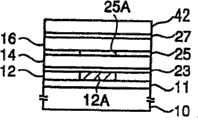
图9表示根据本发明第七实施例的半导体器件50的结构。FIG. 9 shows the structure of a
参见图9,该半导体器件包括承载有源器件(未示出)的Si衬底51,其中Si衬底51承载覆盖有源器件的绝缘膜52。在绝缘膜52上,形成第一层互连图形53A,在绝缘膜52上形成层间绝缘膜53以覆盖互连图形53A。此外,层间绝缘膜53上承载第二层互连图形54A,并在层间绝缘膜53上形成互连图形54以覆盖第二层互连图形54A。用氮化硅钝化膜55覆盖层间绝缘膜54的表面。Referring to FIG. 9, the semiconductor device includes a
图10表示形成氮化硅钝化膜55的工艺。FIG. 10 shows the process of forming the silicon
参见图10,在形成层间绝缘膜54时,在步骤1中将半导体器件50引入到旋涂器单元中。由此,在层间绝缘膜54的表面上对应钝化膜55形成有机硅氮烷化合物的旋涂膜,例如成分为(SiH2NH)n(其中n是1或更大的整数)的化合物膜。在步骤1中,在100℃或以下的温度下对如此形成的旋涂膜进行烘焙工艺,用于去掉溶剂,结果是获得稳定的氮化硅膜。Referring to FIG. 10 , in forming the
另一方面,在图10的步骤1中获得的氮化硅膜必然含有氧,因此本发明的工艺进行到步骤2,其中将半导体器件50安装到等离子体处理装置如图2的等离子体CVD装置中。在那里,利用含有NH3、N2、H2等的等离子气体处理氮化硅膜的表面,并且该膜中的氧部分地被氮代替。由此,在聚合反应在旋涂膜55中完成之前,本例进行了步骤2的等离子体处理。On the other hand, the silicon nitride film obtained in
作为这种等离子体处理的结果,氮化硅膜55被转换成具有表示为SiNCH或SiONCH的化学式的膜。如此获得的膜具有优异的抗温度特性和抗化学物质的特性。As a result of this plasma treatment, the
通常,通过在步骤1之后在N2气氛中进行热处理,可以获得氮氧化物膜。然而,用于转换该膜的工艺需要400℃或更高的高温。此外,尽管使用这种高温,膜质量的转换也不充分。Usually, an oxynitride film can be obtained by performing heat treatment in aN2 atmosphere after
在本发明中,应该注意到步骤2的等离子体处理是在完成旋涂膜55中的聚合反应之前进行的。因此,可以在低温实现有效表面改性反应。应该注意到,可以采用NH3和SiH4作为等离子体气体在350℃或以下的衬底温度下同时采用100-1000W的等离子体功率进行这种等离子体处理。优选,设定等离子体处理的进行,以便减少膜55中的OH基,并增加N键的比例。In the present invention, it should be noted that the plasma treatment in Step 2 is performed before the polymerization reaction in the spin-coated
在本例中,应该注意到步骤1的烘焙工艺是在100℃或以下的温度下进行的,因此在聚合反应在旋涂膜55中完成之前进行步骤2的工艺。此外,优选采用单个晶片处理装置,以便连续进行步骤1和步骤2。In this example, it should be noted that the baking process of
应该注意到步骤2的工艺不限于等离子体处理,还可以是在含有N或H的气氛中进行的热处理。例如,可以在含有NH3或N2和H2的气氛中在400℃或更高的温度下进行步骤2的热处理。It should be noted that the process in step 2 is not limited to plasma treatment, but may also be heat treatment in an atmosphere containing N or H. For example, the heat treatment of step 2 may be performed at a temperature of 400° C. or higher in an atmosphere containing NH3 or N2 and H2 .
此外,本发明不限于上述实施例,在不脱离本发明的范围的情况下还可以做出各种改变和修改。In addition, the present invention is not limited to the above-described embodiments, and various changes and modifications can be made without departing from the scope of the present invention.
工业实用性Industrial Applicability
根据本发明,通过在CVD源中的有机硅氮烷键保持在膜中的条件下进行其中含有有机硅氮烷键的有机Si化合物的CVD工艺,可以获得SiNCH体系的氮化硅膜。如此形成的氮化硅膜的特征在于低密度和低比介电常数。此外,如此获得氮化硅膜具有优异的粘接性和抗刻蚀性的有利特征并作为抵抗金属元素如Cu等的有效扩散阻挡层的特性。通过采用本发明的氮化硅膜可以形成具有小杂散电容的多层互连结构。According to the present invention, a SiNCH system silicon nitride film can be obtained by performing a CVD process of an organic Si compound containing an organosilazane bond therein under the condition that the organosilazane bond in the CVD source remains in the film. The silicon nitride film thus formed is characterized by low density and low specific permittivity. In addition, the silicon nitride film thus obtained has advantageous features of excellent adhesion and etch resistance and characteristics as an effective diffusion barrier against metal elements such as Cu and the like. A multilayer interconnect structure with small stray capacitance can be formed by using the silicon nitride film of the present invention.
Claims (22)
Applications Claiming Priority (3)
| Application Number | Priority Date | Filing Date | Title |
|---|---|---|---|
| JP2000248922 | 2000-08-18 | ||
| JP2000248922 | 2000-08-18 | ||
| JP2000-248922 | 2000-08-18 |
Publications (2)
| Publication Number | Publication Date |
|---|---|
| CN1446374A CN1446374A (en) | 2003-10-01 |
| CN100431110Ctrue CN100431110C (en) | 2008-11-05 |
Family
ID=18738734
Family Applications (1)
| Application Number | Title | Priority Date | Filing Date |
|---|---|---|---|
| CNB018140505AExpired - Fee RelatedCN100431110C (en) | 2000-08-18 | 2001-08-16 | Method for forming low-dielectric silicon nitride film, semiconductor device and manufacturing process thereof |
Country Status (9)
| Country | Link |
|---|---|
| US (1) | US6890869B2 (en) |
| EP (1) | EP1316108B9 (en) |
| JP (1) | JP4048112B2 (en) |
| KR (1) | KR100533198B1 (en) |
| CN (1) | CN100431110C (en) |
| AU (1) | AU2001278749A1 (en) |
| DE (1) | DE60127973T2 (en) |
| TW (1) | TW554442B (en) |
| WO (1) | WO2002017374A1 (en) |
Families Citing this family (366)
| Publication number | Priority date | Publication date | Assignee | Title |
|---|---|---|---|---|
| US20020086547A1 (en)* | 2000-02-17 | 2002-07-04 | Applied Materials, Inc. | Etch pattern definition using a CVD organic layer as an anti-reflection coating and hardmask |
| JP2004111538A (en)* | 2002-09-17 | 2004-04-08 | Fujitsu Ltd | Semiconductor device, semiconductor device manufacturing method and evaluation method, and process condition evaluation method |
| JP3898133B2 (en) | 2003-01-14 | 2007-03-28 | Necエレクトロニクス株式会社 | A method of forming a SiCHN film. |
| JP4068072B2 (en)* | 2003-01-29 | 2008-03-26 | Necエレクトロニクス株式会社 | Semiconductor device and manufacturing method thereof |
| JP4746829B2 (en) | 2003-01-31 | 2011-08-10 | ルネサスエレクトロニクス株式会社 | Semiconductor device and manufacturing method thereof |
| US7001844B2 (en)* | 2004-04-30 | 2006-02-21 | International Business Machines Corporation | Material for contact etch layer to enhance device performance |
| US7129187B2 (en)* | 2004-07-14 | 2006-10-31 | Tokyo Electron Limited | Low-temperature plasma-enhanced chemical vapor deposition of silicon-nitrogen-containing films |
| TWI263103B (en)* | 2004-12-29 | 2006-10-01 | Au Optronics Corp | Copper gate electrode of liquid crystal display device and method of fabricating the same |
| TWI273329B (en)* | 2004-12-29 | 2007-02-11 | Au Optronics Corp | Copper gate electrode of liquid crystal display device and method of fabricating the same |
| JP5007511B2 (en) | 2006-02-14 | 2012-08-22 | 富士通株式会社 | Exposure light shielding film forming material, multilayer wiring, manufacturing method thereof, and semiconductor device |
| US7718553B2 (en)* | 2006-09-21 | 2010-05-18 | Asm Japan K.K. | Method for forming insulation film having high density |
| US7749802B2 (en)* | 2007-01-09 | 2010-07-06 | International Business Machines Corporation | Process for chemical vapor deposition of materials with via filling capability and structure formed thereby |
| US7781352B2 (en)* | 2007-06-06 | 2010-08-24 | Asm Japan K.K. | Method for forming inorganic silazane-based dielectric film |
| US7651959B2 (en) | 2007-12-03 | 2010-01-26 | Asm Japan K.K. | Method for forming silazane-based dielectric film |
| DE102008016425B4 (en)* | 2008-03-31 | 2015-11-19 | Advanced Micro Devices, Inc. | A method of patterning a metallization layer by reducing degradation of the dielectric material caused by resist removal |
| US7622369B1 (en) | 2008-05-30 | 2009-11-24 | Asm Japan K.K. | Device isolation technology on semiconductor substrate |
| US10378106B2 (en) | 2008-11-14 | 2019-08-13 | Asm Ip Holding B.V. | Method of forming insulation film by modified PEALD |
| US8765233B2 (en)* | 2008-12-09 | 2014-07-01 | Asm Japan K.K. | Method for forming low-carbon CVD film for filling trenches |
| US9394608B2 (en) | 2009-04-06 | 2016-07-19 | Asm America, Inc. | Semiconductor processing reactor and components thereof |
| KR100953736B1 (en)* | 2009-07-27 | 2010-04-19 | 주식회사 아토 | Deposition apparatus and method of manufacturing a semiconductor device |
| US8802201B2 (en) | 2009-08-14 | 2014-08-12 | Asm America, Inc. | Systems and methods for thin-film deposition of metal oxides using excited nitrogen-oxygen species |
| KR101732187B1 (en)* | 2009-09-03 | 2017-05-02 | 에이에스엠 저펜 가부시기가이샤 | METHOD OF FORMING CONFORMAL DIELECTRIC FILM HAVING Si-N BONDS BY PECVD |
| US8912353B2 (en) | 2010-06-02 | 2014-12-16 | Air Products And Chemicals, Inc. | Organoaminosilane precursors and methods for depositing films comprising same |
| JP5874230B2 (en)* | 2010-08-27 | 2016-03-02 | 東ソー株式会社 | Sealing film material, sealing film and application |
| US8771807B2 (en) | 2011-05-24 | 2014-07-08 | Air Products And Chemicals, Inc. | Organoaminosilane precursors and methods for making and using same |
| US9312155B2 (en) | 2011-06-06 | 2016-04-12 | Asm Japan K.K. | High-throughput semiconductor-processing apparatus equipped with multiple dual-chamber modules |
| US10854498B2 (en) | 2011-07-15 | 2020-12-01 | Asm Ip Holding B.V. | Wafer-supporting device and method for producing same |
| US20130023129A1 (en) | 2011-07-20 | 2013-01-24 | Asm America, Inc. | Pressure transmitter for a semiconductor processing environment |
| US9017481B1 (en) | 2011-10-28 | 2015-04-28 | Asm America, Inc. | Process feed management for semiconductor substrate processing |
| US9659799B2 (en) | 2012-08-28 | 2017-05-23 | Asm Ip Holding B.V. | Systems and methods for dynamic semiconductor process scheduling |
| US10714315B2 (en) | 2012-10-12 | 2020-07-14 | Asm Ip Holdings B.V. | Semiconductor reaction chamber showerhead |
| US20160376700A1 (en) | 2013-02-01 | 2016-12-29 | Asm Ip Holding B.V. | System for treatment of deposition reactor |
| JP6318433B2 (en)* | 2013-11-28 | 2018-05-09 | 大陽日酸株式会社 | Silicon nitride film forming method and silicon nitride film |
| US10683571B2 (en) | 2014-02-25 | 2020-06-16 | Asm Ip Holding B.V. | Gas supply manifold and method of supplying gases to chamber using same |
| US10167557B2 (en) | 2014-03-18 | 2019-01-01 | Asm Ip Holding B.V. | Gas distribution system, reactor including the system, and methods of using the same |
| US11015245B2 (en) | 2014-03-19 | 2021-05-25 | Asm Ip Holding B.V. | Gas-phase reactor and system having exhaust plenum and components thereof |
| US10858737B2 (en) | 2014-07-28 | 2020-12-08 | Asm Ip Holding B.V. | Showerhead assembly and components thereof |
| US9890456B2 (en) | 2014-08-21 | 2018-02-13 | Asm Ip Holding B.V. | Method and system for in situ formation of gas-phase compounds |
| US10941490B2 (en) | 2014-10-07 | 2021-03-09 | Asm Ip Holding B.V. | Multiple temperature range susceptor, assembly, reactor and system including the susceptor, and methods of using the same |
| US9657845B2 (en) | 2014-10-07 | 2017-05-23 | Asm Ip Holding B.V. | Variable conductance gas distribution apparatus and method |
| JP6236709B2 (en)* | 2014-10-14 | 2017-11-29 | 大陽日酸株式会社 | Silicon nitride film manufacturing method and silicon nitride film |
| KR102079501B1 (en)* | 2014-10-24 | 2020-02-20 | 버슘머트리얼즈 유에스, 엘엘씨 | Compositions and methods using same for deposition of silicon-containing film |
| KR102263121B1 (en) | 2014-12-22 | 2021-06-09 | 에이에스엠 아이피 홀딩 비.브이. | Semiconductor device and manufacuring method thereof |
| US10529542B2 (en) | 2015-03-11 | 2020-01-07 | Asm Ip Holdings B.V. | Cross-flow reactor and method |
| US10276355B2 (en) | 2015-03-12 | 2019-04-30 | Asm Ip Holding B.V. | Multi-zone reactor, system including the reactor, and method of using the same |
| US10458018B2 (en) | 2015-06-26 | 2019-10-29 | Asm Ip Holding B.V. | Structures including metal carbide material, devices including the structures, and methods of forming same |
| US10600673B2 (en) | 2015-07-07 | 2020-03-24 | Asm Ip Holding B.V. | Magnetic susceptor to baseplate seal |
| US9960072B2 (en) | 2015-09-29 | 2018-05-01 | Asm Ip Holding B.V. | Variable adjustment for precise matching of multiple chamber cavity housings |
| US10211308B2 (en) | 2015-10-21 | 2019-02-19 | Asm Ip Holding B.V. | NbMC layers |
| US11139308B2 (en) | 2015-12-29 | 2021-10-05 | Asm Ip Holding B.V. | Atomic layer deposition of III-V compounds to form V-NAND devices |
| US9859156B2 (en)* | 2015-12-30 | 2018-01-02 | Taiwan Semiconductor Manufacturing Co., Ltd. | Interconnection structure with sidewall dielectric protection layer |
| US10468251B2 (en) | 2016-02-19 | 2019-11-05 | Asm Ip Holding B.V. | Method for forming spacers using silicon nitride film for spacer-defined multiple patterning |
| US10529554B2 (en) | 2016-02-19 | 2020-01-07 | Asm Ip Holding B.V. | Method for forming silicon nitride film selectively on sidewalls or flat surfaces of trenches |
| WO2017154202A1 (en) | 2016-03-11 | 2017-09-14 | 大陽日酸株式会社 | Method for producing silicon nitride film, and silicon nitride film |
| US10343920B2 (en) | 2016-03-18 | 2019-07-09 | Asm Ip Holding B.V. | Aligned carbon nanotubes |
| US10865475B2 (en) | 2016-04-21 | 2020-12-15 | Asm Ip Holding B.V. | Deposition of metal borides and silicides |
| US10190213B2 (en) | 2016-04-21 | 2019-01-29 | Asm Ip Holding B.V. | Deposition of metal borides |
| US10367080B2 (en) | 2016-05-02 | 2019-07-30 | Asm Ip Holding B.V. | Method of forming a germanium oxynitride film |
| US10032628B2 (en) | 2016-05-02 | 2018-07-24 | Asm Ip Holding B.V. | Source/drain performance through conformal solid state doping |
| US11453943B2 (en) | 2016-05-25 | 2022-09-27 | Asm Ip Holding B.V. | Method for forming carbon-containing silicon/metal oxide or nitride film by ALD using silicon precursor and hydrocarbon precursor |
| WO2017218561A1 (en) | 2016-06-13 | 2017-12-21 | Gvd Coproraton | Methods for plasma depositing polymers comprising cyclic siloxanes and related compositions and articles |
| US11679412B2 (en) | 2016-06-13 | 2023-06-20 | Gvd Corporation | Methods for plasma depositing polymers comprising cyclic siloxanes and related compositions and articles |
| US10388509B2 (en) | 2016-06-28 | 2019-08-20 | Asm Ip Holding B.V. | Formation of epitaxial layers via dislocation filtering |
| US10612137B2 (en) | 2016-07-08 | 2020-04-07 | Asm Ip Holdings B.V. | Organic reactants for atomic layer deposition |
| US9859151B1 (en) | 2016-07-08 | 2018-01-02 | Asm Ip Holding B.V. | Selective film deposition method to form air gaps |
| US10714385B2 (en) | 2016-07-19 | 2020-07-14 | Asm Ip Holding B.V. | Selective deposition of tungsten |
| US9887082B1 (en) | 2016-07-28 | 2018-02-06 | Asm Ip Holding B.V. | Method and apparatus for filling a gap |
| US10395919B2 (en) | 2016-07-28 | 2019-08-27 | Asm Ip Holding B.V. | Method and apparatus for filling a gap |
| US9812320B1 (en) | 2016-07-28 | 2017-11-07 | Asm Ip Holding B.V. | Method and apparatus for filling a gap |
| KR102532607B1 (en) | 2016-07-28 | 2023-05-15 | 에이에스엠 아이피 홀딩 비.브이. | Substrate processing apparatus and method of operating the same |
| US10410943B2 (en) | 2016-10-13 | 2019-09-10 | Asm Ip Holding B.V. | Method for passivating a surface of a semiconductor and related systems |
| US10643826B2 (en) | 2016-10-26 | 2020-05-05 | Asm Ip Holdings B.V. | Methods for thermally calibrating reaction chambers |
| US11532757B2 (en) | 2016-10-27 | 2022-12-20 | Asm Ip Holding B.V. | Deposition of charge trapping layers |
| US10229833B2 (en) | 2016-11-01 | 2019-03-12 | Asm Ip Holding B.V. | Methods for forming a transition metal nitride film on a substrate by atomic layer deposition and related semiconductor device structures |
| US10714350B2 (en) | 2016-11-01 | 2020-07-14 | ASM IP Holdings, B.V. | Methods for forming a transition metal niobium nitride film on a substrate by atomic layer deposition and related semiconductor device structures |
| US10435790B2 (en) | 2016-11-01 | 2019-10-08 | Asm Ip Holding B.V. | Method of subatmospheric plasma-enhanced ALD using capacitively coupled electrodes with narrow gap |
| US10134757B2 (en) | 2016-11-07 | 2018-11-20 | Asm Ip Holding B.V. | Method of processing a substrate and a device manufactured by using the method |
| KR102546317B1 (en) | 2016-11-15 | 2023-06-21 | 에이에스엠 아이피 홀딩 비.브이. | Gas supply unit and substrate processing apparatus including the same |
| US10340135B2 (en) | 2016-11-28 | 2019-07-02 | Asm Ip Holding B.V. | Method of topologically restricted plasma-enhanced cyclic deposition of silicon or metal nitride |
| KR102762543B1 (en) | 2016-12-14 | 2025-02-05 | 에이에스엠 아이피 홀딩 비.브이. | Substrate processing apparatus |
| US11447861B2 (en) | 2016-12-15 | 2022-09-20 | Asm Ip Holding B.V. | Sequential infiltration synthesis apparatus and a method of forming a patterned structure |
| US11581186B2 (en) | 2016-12-15 | 2023-02-14 | Asm Ip Holding B.V. | Sequential infiltration synthesis apparatus |
| KR102700194B1 (en) | 2016-12-19 | 2024-08-28 | 에이에스엠 아이피 홀딩 비.브이. | Substrate processing apparatus |
| US10269558B2 (en) | 2016-12-22 | 2019-04-23 | Asm Ip Holding B.V. | Method of forming a structure on a substrate |
| US10867788B2 (en) | 2016-12-28 | 2020-12-15 | Asm Ip Holding B.V. | Method of forming a structure on a substrate |
| US11390950B2 (en) | 2017-01-10 | 2022-07-19 | Asm Ip Holding B.V. | Reactor system and method to reduce residue buildup during a film deposition process |
| US10655221B2 (en) | 2017-02-09 | 2020-05-19 | Asm Ip Holding B.V. | Method for depositing oxide film by thermal ALD and PEALD |
| US10468261B2 (en) | 2017-02-15 | 2019-11-05 | Asm Ip Holding B.V. | Methods for forming a metallic film on a substrate by cyclical deposition and related semiconductor device structures |
| US10529563B2 (en) | 2017-03-29 | 2020-01-07 | Asm Ip Holdings B.V. | Method for forming doped metal oxide films on a substrate by cyclical deposition and related semiconductor device structures |
| KR102457289B1 (en) | 2017-04-25 | 2022-10-21 | 에이에스엠 아이피 홀딩 비.브이. | Method for depositing a thin film and manufacturing a semiconductor device |
| US10892156B2 (en) | 2017-05-08 | 2021-01-12 | Asm Ip Holding B.V. | Methods for forming a silicon nitride film on a substrate and related semiconductor device structures |
| US10446393B2 (en) | 2017-05-08 | 2019-10-15 | Asm Ip Holding B.V. | Methods for forming silicon-containing epitaxial layers and related semiconductor device structures |
| US10770286B2 (en) | 2017-05-08 | 2020-09-08 | Asm Ip Holdings B.V. | Methods for selectively forming a silicon nitride film on a substrate and related semiconductor device structures |
| US10504742B2 (en) | 2017-05-31 | 2019-12-10 | Asm Ip Holding B.V. | Method of atomic layer etching using hydrogen plasma |
| US10886123B2 (en) | 2017-06-02 | 2021-01-05 | Asm Ip Holding B.V. | Methods for forming low temperature semiconductor layers and related semiconductor device structures |
| US12040200B2 (en) | 2017-06-20 | 2024-07-16 | Asm Ip Holding B.V. | Semiconductor processing apparatus and methods for calibrating a semiconductor processing apparatus |
| US11306395B2 (en) | 2017-06-28 | 2022-04-19 | Asm Ip Holding B.V. | Methods for depositing a transition metal nitride film on a substrate by atomic layer deposition and related deposition apparatus |
| US10685834B2 (en) | 2017-07-05 | 2020-06-16 | Asm Ip Holdings B.V. | Methods for forming a silicon germanium tin layer and related semiconductor device structures |
| KR20190009245A (en) | 2017-07-18 | 2019-01-28 | 에이에스엠 아이피 홀딩 비.브이. | Methods for forming a semiconductor device structure and related semiconductor device structures |
| US11374112B2 (en) | 2017-07-19 | 2022-06-28 | Asm Ip Holding B.V. | Method for depositing a group IV semiconductor and related semiconductor device structures |
| US10541333B2 (en) | 2017-07-19 | 2020-01-21 | Asm Ip Holding B.V. | Method for depositing a group IV semiconductor and related semiconductor device structures |
| US11018002B2 (en) | 2017-07-19 | 2021-05-25 | Asm Ip Holding B.V. | Method for selectively depositing a Group IV semiconductor and related semiconductor device structures |
| US10605530B2 (en) | 2017-07-26 | 2020-03-31 | Asm Ip Holding B.V. | Assembly of a liner and a flange for a vertical furnace as well as the liner and the vertical furnace |
| US10590535B2 (en) | 2017-07-26 | 2020-03-17 | Asm Ip Holdings B.V. | Chemical treatment, deposition and/or infiltration apparatus and method for using the same |
| TWI815813B (en) | 2017-08-04 | 2023-09-21 | 荷蘭商Asm智慧財產控股公司 | Showerhead assembly for distributing a gas within a reaction chamber |
| US10770336B2 (en) | 2017-08-08 | 2020-09-08 | Asm Ip Holding B.V. | Substrate lift mechanism and reactor including same |
| US10692741B2 (en) | 2017-08-08 | 2020-06-23 | Asm Ip Holdings B.V. | Radiation shield |
| US11139191B2 (en) | 2017-08-09 | 2021-10-05 | Asm Ip Holding B.V. | Storage apparatus for storing cassettes for substrates and processing apparatus equipped therewith |
| US11769682B2 (en) | 2017-08-09 | 2023-09-26 | Asm Ip Holding B.V. | Storage apparatus for storing cassettes for substrates and processing apparatus equipped therewith |
| US10249524B2 (en) | 2017-08-09 | 2019-04-02 | Asm Ip Holding B.V. | Cassette holder assembly for a substrate cassette and holding member for use in such assembly |
| USD900036S1 (en) | 2017-08-24 | 2020-10-27 | Asm Ip Holding B.V. | Heater electrical connector and adapter |
| US11830730B2 (en) | 2017-08-29 | 2023-11-28 | Asm Ip Holding B.V. | Layer forming method and apparatus |
| KR102491945B1 (en) | 2017-08-30 | 2023-01-26 | 에이에스엠 아이피 홀딩 비.브이. | Substrate processing apparatus |
| US11295980B2 (en) | 2017-08-30 | 2022-04-05 | Asm Ip Holding B.V. | Methods for depositing a molybdenum metal film over a dielectric surface of a substrate by a cyclical deposition process and related semiconductor device structures |
| US11056344B2 (en) | 2017-08-30 | 2021-07-06 | Asm Ip Holding B.V. | Layer forming method |
| KR102401446B1 (en) | 2017-08-31 | 2022-05-24 | 에이에스엠 아이피 홀딩 비.브이. | Substrate processing apparatus |
| US10607895B2 (en) | 2017-09-18 | 2020-03-31 | Asm Ip Holdings B.V. | Method for forming a semiconductor device structure comprising a gate fill metal |
| KR102630301B1 (en) | 2017-09-21 | 2024-01-29 | 에이에스엠 아이피 홀딩 비.브이. | Method of sequential infiltration synthesis treatment of infiltrateable material and structures and devices formed using same |
| US10844484B2 (en) | 2017-09-22 | 2020-11-24 | Asm Ip Holding B.V. | Apparatus for dispensing a vapor phase reactant to a reaction chamber and related methods |
| US10658205B2 (en) | 2017-09-28 | 2020-05-19 | Asm Ip Holdings B.V. | Chemical dispensing apparatus and methods for dispensing a chemical to a reaction chamber |
| US10403504B2 (en) | 2017-10-05 | 2019-09-03 | Asm Ip Holding B.V. | Method for selectively depositing a metallic film on a substrate |
| US10319588B2 (en) | 2017-10-10 | 2019-06-11 | Asm Ip Holding B.V. | Method for depositing a metal chalcogenide on a substrate by cyclical deposition |
| US10923344B2 (en) | 2017-10-30 | 2021-02-16 | Asm Ip Holding B.V. | Methods for forming a semiconductor structure and related semiconductor structures |
| US10910262B2 (en) | 2017-11-16 | 2021-02-02 | Asm Ip Holding B.V. | Method of selectively depositing a capping layer structure on a semiconductor device structure |
| KR102443047B1 (en) | 2017-11-16 | 2022-09-14 | 에이에스엠 아이피 홀딩 비.브이. | Method of processing a substrate and a device manufactured by the same |
| US11022879B2 (en) | 2017-11-24 | 2021-06-01 | Asm Ip Holding B.V. | Method of forming an enhanced unexposed photoresist layer |
| WO2019103613A1 (en) | 2017-11-27 | 2019-05-31 | Asm Ip Holding B.V. | A storage device for storing wafer cassettes for use with a batch furnace |
| CN111344522B (en) | 2017-11-27 | 2022-04-12 | 阿斯莫Ip控股公司 | Including clean mini-environment device |
| US10872771B2 (en) | 2018-01-16 | 2020-12-22 | Asm Ip Holding B. V. | Method for depositing a material film on a substrate within a reaction chamber by a cyclical deposition process and related device structures |
| KR102695659B1 (en) | 2018-01-19 | 2024-08-14 | 에이에스엠 아이피 홀딩 비.브이. | Method for depositing a gap filling layer by plasma assisted deposition |
| TWI799494B (en) | 2018-01-19 | 2023-04-21 | 荷蘭商Asm 智慧財產控股公司 | Deposition method |
| USD903477S1 (en) | 2018-01-24 | 2020-12-01 | Asm Ip Holdings B.V. | Metal clamp |
| US11018047B2 (en) | 2018-01-25 | 2021-05-25 | Asm Ip Holding B.V. | Hybrid lift pin |
| US10535516B2 (en) | 2018-02-01 | 2020-01-14 | Asm Ip Holdings B.V. | Method for depositing a semiconductor structure on a surface of a substrate and related semiconductor structures |
| USD880437S1 (en) | 2018-02-01 | 2020-04-07 | Asm Ip Holding B.V. | Gas supply plate for semiconductor manufacturing apparatus |
| US11081345B2 (en) | 2018-02-06 | 2021-08-03 | Asm Ip Holding B.V. | Method of post-deposition treatment for silicon oxide film |
| US10896820B2 (en) | 2018-02-14 | 2021-01-19 | Asm Ip Holding B.V. | Method for depositing a ruthenium-containing film on a substrate by a cyclical deposition process |
| WO2019158960A1 (en) | 2018-02-14 | 2019-08-22 | Asm Ip Holding B.V. | A method for depositing a ruthenium-containing film on a substrate by a cyclical deposition process |
| US10731249B2 (en) | 2018-02-15 | 2020-08-04 | Asm Ip Holding B.V. | Method of forming a transition metal containing film on a substrate by a cyclical deposition process, a method for supplying a transition metal halide compound to a reaction chamber, and related vapor deposition apparatus |
| KR102636427B1 (en) | 2018-02-20 | 2024-02-13 | 에이에스엠 아이피 홀딩 비.브이. | Substrate processing method and apparatus |
| US10658181B2 (en) | 2018-02-20 | 2020-05-19 | Asm Ip Holding B.V. | Method of spacer-defined direct patterning in semiconductor fabrication |
| US10975470B2 (en) | 2018-02-23 | 2021-04-13 | Asm Ip Holding B.V. | Apparatus for detecting or monitoring for a chemical precursor in a high temperature environment |
| US11473195B2 (en) | 2018-03-01 | 2022-10-18 | Asm Ip Holding B.V. | Semiconductor processing apparatus and a method for processing a substrate |
| US11629406B2 (en) | 2018-03-09 | 2023-04-18 | Asm Ip Holding B.V. | Semiconductor processing apparatus comprising one or more pyrometers for measuring a temperature of a substrate during transfer of the substrate |
| US11114283B2 (en) | 2018-03-16 | 2021-09-07 | Asm Ip Holding B.V. | Reactor, system including the reactor, and methods of manufacturing and using same |
| KR102646467B1 (en) | 2018-03-27 | 2024-03-11 | 에이에스엠 아이피 홀딩 비.브이. | Method of forming an electrode on a substrate and a semiconductor device structure including an electrode |
| US10510536B2 (en) | 2018-03-29 | 2019-12-17 | Asm Ip Holding B.V. | Method of depositing a co-doped polysilicon film on a surface of a substrate within a reaction chamber |
| US11088002B2 (en) | 2018-03-29 | 2021-08-10 | Asm Ip Holding B.V. | Substrate rack and a substrate processing system and method |
| US11230766B2 (en) | 2018-03-29 | 2022-01-25 | Asm Ip Holding B.V. | Substrate processing apparatus and method |
| KR102501472B1 (en) | 2018-03-30 | 2023-02-20 | 에이에스엠 아이피 홀딩 비.브이. | Substrate processing method |
| KR102600229B1 (en) | 2018-04-09 | 2023-11-10 | 에이에스엠 아이피 홀딩 비.브이. | Substrate supporting device, substrate processing apparatus including the same and substrate processing method |
| TWI811348B (en) | 2018-05-08 | 2023-08-11 | 荷蘭商Asm 智慧財產控股公司 | Methods for depositing an oxide film on a substrate by a cyclical deposition process and related device structures |
| US12025484B2 (en) | 2018-05-08 | 2024-07-02 | Asm Ip Holding B.V. | Thin film forming method |
| US12272527B2 (en) | 2018-05-09 | 2025-04-08 | Asm Ip Holding B.V. | Apparatus for use with hydrogen radicals and method of using same |
| KR20190129718A (en) | 2018-05-11 | 2019-11-20 | 에이에스엠 아이피 홀딩 비.브이. | Methods for forming a doped metal carbide film on a substrate and related semiconductor device structures |
| KR102596988B1 (en) | 2018-05-28 | 2023-10-31 | 에이에스엠 아이피 홀딩 비.브이. | Method of processing a substrate and a device manufactured by the same |
| US11718913B2 (en) | 2018-06-04 | 2023-08-08 | Asm Ip Holding B.V. | Gas distribution system and reactor system including same |
| TWI840362B (en) | 2018-06-04 | 2024-05-01 | 荷蘭商Asm Ip私人控股有限公司 | Wafer handling chamber with moisture reduction |
| US11286562B2 (en) | 2018-06-08 | 2022-03-29 | Asm Ip Holding B.V. | Gas-phase chemical reactor and method of using same |
| US10797133B2 (en) | 2018-06-21 | 2020-10-06 | Asm Ip Holding B.V. | Method for depositing a phosphorus doped silicon arsenide film and related semiconductor device structures |
| KR102568797B1 (en) | 2018-06-21 | 2023-08-21 | 에이에스엠 아이피 홀딩 비.브이. | Substrate processing system |
| KR102854019B1 (en) | 2018-06-27 | 2025-09-02 | 에이에스엠 아이피 홀딩 비.브이. | Periodic deposition method for forming a metal-containing material and films and structures comprising the metal-containing material |
| TWI873894B (en) | 2018-06-27 | 2025-02-21 | 荷蘭商Asm Ip私人控股有限公司 | Cyclic deposition methods for forming metal-containing material and films and structures including the metal-containing material |
| KR102686758B1 (en) | 2018-06-29 | 2024-07-18 | 에이에스엠 아이피 홀딩 비.브이. | Method for depositing a thin film and manufacturing a semiconductor device |
| US10612136B2 (en) | 2018-06-29 | 2020-04-07 | ASM IP Holding, B.V. | Temperature-controlled flange and reactor system including same |
| US10388513B1 (en) | 2018-07-03 | 2019-08-20 | Asm Ip Holding B.V. | Method for depositing silicon-free carbon-containing film as gap-fill layer by pulse plasma-assisted deposition |
| US10755922B2 (en) | 2018-07-03 | 2020-08-25 | Asm Ip Holding B.V. | Method for depositing silicon-free carbon-containing film as gap-fill layer by pulse plasma-assisted deposition |
| US10767789B2 (en) | 2018-07-16 | 2020-09-08 | Asm Ip Holding B.V. | Diaphragm valves, valve components, and methods for forming valve components |
| US10483099B1 (en) | 2018-07-26 | 2019-11-19 | Asm Ip Holding B.V. | Method for forming thermally stable organosilicon polymer film |
| US11053591B2 (en) | 2018-08-06 | 2021-07-06 | Asm Ip Holding B.V. | Multi-port gas injection system and reactor system including same |
| US10883175B2 (en) | 2018-08-09 | 2021-01-05 | Asm Ip Holding B.V. | Vertical furnace for processing substrates and a liner for use therein |
| US10829852B2 (en) | 2018-08-16 | 2020-11-10 | Asm Ip Holding B.V. | Gas distribution device for a wafer processing apparatus |
| US11430674B2 (en) | 2018-08-22 | 2022-08-30 | Asm Ip Holding B.V. | Sensor array, apparatus for dispensing a vapor phase reactant to a reaction chamber and related methods |
| KR102707956B1 (en) | 2018-09-11 | 2024-09-19 | 에이에스엠 아이피 홀딩 비.브이. | Method for deposition of a thin film |
| US11024523B2 (en) | 2018-09-11 | 2021-06-01 | Asm Ip Holding B.V. | Substrate processing apparatus and method |
| US11049751B2 (en) | 2018-09-14 | 2021-06-29 | Asm Ip Holding B.V. | Cassette supply system to store and handle cassettes and processing apparatus equipped therewith |
| CN110970344B (en) | 2018-10-01 | 2024-10-25 | Asmip控股有限公司 | Substrate holding apparatus, system comprising the same and method of using the same |
| US11232963B2 (en) | 2018-10-03 | 2022-01-25 | Asm Ip Holding B.V. | Substrate processing apparatus and method |
| KR102592699B1 (en) | 2018-10-08 | 2023-10-23 | 에이에스엠 아이피 홀딩 비.브이. | Substrate support unit and apparatuses for depositing thin film and processing the substrate including the same |
| US10847365B2 (en) | 2018-10-11 | 2020-11-24 | Asm Ip Holding B.V. | Method of forming conformal silicon carbide film by cyclic CVD |
| US10811256B2 (en) | 2018-10-16 | 2020-10-20 | Asm Ip Holding B.V. | Method for etching a carbon-containing feature |
| KR102546322B1 (en) | 2018-10-19 | 2023-06-21 | 에이에스엠 아이피 홀딩 비.브이. | Substrate processing apparatus and substrate processing method |
| KR102605121B1 (en) | 2018-10-19 | 2023-11-23 | 에이에스엠 아이피 홀딩 비.브이. | Substrate processing apparatus and substrate processing method |
| USD948463S1 (en) | 2018-10-24 | 2022-04-12 | Asm Ip Holding B.V. | Susceptor for semiconductor substrate supporting apparatus |
| US10381219B1 (en) | 2018-10-25 | 2019-08-13 | Asm Ip Holding B.V. | Methods for forming a silicon nitride film |
| US12378665B2 (en) | 2018-10-26 | 2025-08-05 | Asm Ip Holding B.V. | High temperature coatings for a preclean and etch apparatus and related methods |
| US11087997B2 (en) | 2018-10-31 | 2021-08-10 | Asm Ip Holding B.V. | Substrate processing apparatus for processing substrates |
| KR102748291B1 (en) | 2018-11-02 | 2024-12-31 | 에이에스엠 아이피 홀딩 비.브이. | Substrate support unit and substrate processing apparatus including the same |
| US11572620B2 (en) | 2018-11-06 | 2023-02-07 | Asm Ip Holding B.V. | Methods for selectively depositing an amorphous silicon film on a substrate |
| US11031242B2 (en) | 2018-11-07 | 2021-06-08 | Asm Ip Holding B.V. | Methods for depositing a boron doped silicon germanium film |
| US10818758B2 (en) | 2018-11-16 | 2020-10-27 | Asm Ip Holding B.V. | Methods for forming a metal silicate film on a substrate in a reaction chamber and related semiconductor device structures |
| US10847366B2 (en) | 2018-11-16 | 2020-11-24 | Asm Ip Holding B.V. | Methods for depositing a transition metal chalcogenide film on a substrate by a cyclical deposition process |
| US10559458B1 (en) | 2018-11-26 | 2020-02-11 | Asm Ip Holding B.V. | Method of forming oxynitride film |
| US12040199B2 (en) | 2018-11-28 | 2024-07-16 | Asm Ip Holding B.V. | Substrate processing apparatus for processing substrates |
| US11217444B2 (en) | 2018-11-30 | 2022-01-04 | Asm Ip Holding B.V. | Method for forming an ultraviolet radiation responsive metal oxide-containing film |
| KR102636428B1 (en) | 2018-12-04 | 2024-02-13 | 에이에스엠 아이피 홀딩 비.브이. | A method for cleaning a substrate processing apparatus |
| US11158513B2 (en) | 2018-12-13 | 2021-10-26 | Asm Ip Holding B.V. | Methods for forming a rhenium-containing film on a substrate by a cyclical deposition process and related semiconductor device structures |
| TWI874340B (en) | 2018-12-14 | 2025-03-01 | 荷蘭商Asm Ip私人控股有限公司 | Method of forming device structure, structure formed by the method and system for performing the method |
| TWI866480B (en) | 2019-01-17 | 2024-12-11 | 荷蘭商Asm Ip 私人控股有限公司 | Methods of forming a transition metal containing film on a substrate by a cyclical deposition process |
| KR102727227B1 (en) | 2019-01-22 | 2024-11-07 | 에이에스엠 아이피 홀딩 비.브이. | Semiconductor processing device |
| CN111524788B (en) | 2019-02-01 | 2023-11-24 | Asm Ip私人控股有限公司 | Method for forming topologically selective films of silicon oxide |
| KR102626263B1 (en) | 2019-02-20 | 2024-01-16 | 에이에스엠 아이피 홀딩 비.브이. | Cyclical deposition method including treatment step and apparatus for same |
| TWI838458B (en) | 2019-02-20 | 2024-04-11 | 荷蘭商Asm Ip私人控股有限公司 | Apparatus and methods for plug fill deposition in 3-d nand applications |
| TWI873122B (en) | 2019-02-20 | 2025-02-21 | 荷蘭商Asm Ip私人控股有限公司 | Method of filling a recess formed within a surface of a substrate, semiconductor structure formed according to the method, and semiconductor processing apparatus |
| TWI845607B (en) | 2019-02-20 | 2024-06-21 | 荷蘭商Asm Ip私人控股有限公司 | Cyclical deposition method and apparatus for filling a recess formed within a substrate surface |
| TWI842826B (en) | 2019-02-22 | 2024-05-21 | 荷蘭商Asm Ip私人控股有限公司 | Substrate processing apparatus and method for processing substrate |
| US11742198B2 (en) | 2019-03-08 | 2023-08-29 | Asm Ip Holding B.V. | Structure including SiOCN layer and method of forming same |
| KR102782593B1 (en) | 2019-03-08 | 2025-03-14 | 에이에스엠 아이피 홀딩 비.브이. | Structure Including SiOC Layer and Method of Forming Same |
| KR102858005B1 (en) | 2019-03-08 | 2025-09-09 | 에이에스엠 아이피 홀딩 비.브이. | Method for Selective Deposition of Silicon Nitride Layer and Structure Including Selectively-Deposited Silicon Nitride Layer |
| JP2020167398A (en) | 2019-03-28 | 2020-10-08 | エーエスエム・アイピー・ホールディング・ベー・フェー | Door openers and substrate processing equipment provided with door openers |
| KR102809999B1 (en) | 2019-04-01 | 2025-05-19 | 에이에스엠 아이피 홀딩 비.브이. | Method of manufacturing semiconductor device |
| KR20200123380A (en) | 2019-04-19 | 2020-10-29 | 에이에스엠 아이피 홀딩 비.브이. | Layer forming method and apparatus |
| KR20200125453A (en) | 2019-04-24 | 2020-11-04 | 에이에스엠 아이피 홀딩 비.브이. | Gas-phase reactor system and method of using same |
| KR20200130121A (en) | 2019-05-07 | 2020-11-18 | 에이에스엠 아이피 홀딩 비.브이. | Chemical source vessel with dip tube |
| US11289326B2 (en) | 2019-05-07 | 2022-03-29 | Asm Ip Holding B.V. | Method for reforming amorphous carbon polymer film |
| KR20200130652A (en) | 2019-05-10 | 2020-11-19 | 에이에스엠 아이피 홀딩 비.브이. | Method of depositing material onto a surface and structure formed according to the method |
| JP7598201B2 (en) | 2019-05-16 | 2024-12-11 | エーエスエム・アイピー・ホールディング・ベー・フェー | Wafer boat handling apparatus, vertical batch furnace and method |
| JP7612342B2 (en) | 2019-05-16 | 2025-01-14 | エーエスエム・アイピー・ホールディング・ベー・フェー | Wafer boat handling apparatus, vertical batch furnace and method |
| USD947913S1 (en) | 2019-05-17 | 2022-04-05 | Asm Ip Holding B.V. | Susceptor shaft |
| USD975665S1 (en) | 2019-05-17 | 2023-01-17 | Asm Ip Holding B.V. | Susceptor shaft |
| USD935572S1 (en) | 2019-05-24 | 2021-11-09 | Asm Ip Holding B.V. | Gas channel plate |
| USD922229S1 (en) | 2019-06-05 | 2021-06-15 | Asm Ip Holding B.V. | Device for controlling a temperature of a gas supply unit |
| KR20200141002A (en) | 2019-06-06 | 2020-12-17 | 에이에스엠 아이피 홀딩 비.브이. | Method of using a gas-phase reactor system including analyzing exhausted gas |
| KR20200141931A (en) | 2019-06-10 | 2020-12-21 | 에이에스엠 아이피 홀딩 비.브이. | Method for cleaning quartz epitaxial chambers |
| KR20200143254A (en) | 2019-06-11 | 2020-12-23 | 에이에스엠 아이피 홀딩 비.브이. | Method of forming an electronic structure using an reforming gas, system for performing the method, and structure formed using the method |
| USD944946S1 (en) | 2019-06-14 | 2022-03-01 | Asm Ip Holding B.V. | Shower plate |
| USD931978S1 (en) | 2019-06-27 | 2021-09-28 | Asm Ip Holding B.V. | Showerhead vacuum transport |
| KR20210005515A (en) | 2019-07-03 | 2021-01-14 | 에이에스엠 아이피 홀딩 비.브이. | Temperature control assembly for substrate processing apparatus and method of using same |
| JP7499079B2 (en) | 2019-07-09 | 2024-06-13 | エーエスエム・アイピー・ホールディング・ベー・フェー | Plasma device using coaxial waveguide and substrate processing method |
| CN112216646A (en) | 2019-07-10 | 2021-01-12 | Asm Ip私人控股有限公司 | Substrate supporting assembly and substrate processing device comprising same |
| KR20210010307A (en) | 2019-07-16 | 2021-01-27 | 에이에스엠 아이피 홀딩 비.브이. | Substrate processing apparatus |
| KR20210010816A (en) | 2019-07-17 | 2021-01-28 | 에이에스엠 아이피 홀딩 비.브이. | Radical assist ignition plasma system and method |
| KR102860110B1 (en) | 2019-07-17 | 2025-09-16 | 에이에스엠 아이피 홀딩 비.브이. | Methods of forming silicon germanium structures |
| US11643724B2 (en) | 2019-07-18 | 2023-05-09 | Asm Ip Holding B.V. | Method of forming structures using a neutral beam |
| KR20210010817A (en) | 2019-07-19 | 2021-01-28 | 에이에스엠 아이피 홀딩 비.브이. | Method of Forming Topology-Controlled Amorphous Carbon Polymer Film |
| TWI839544B (en) | 2019-07-19 | 2024-04-21 | 荷蘭商Asm Ip私人控股有限公司 | Method of forming topology-controlled amorphous carbon polymer film |
| TWI851767B (en) | 2019-07-29 | 2024-08-11 | 荷蘭商Asm Ip私人控股有限公司 | Methods for selective deposition utilizing n-type dopants and/or alternative dopants to achieve high dopant incorporation |
| US12169361B2 (en) | 2019-07-30 | 2024-12-17 | Asm Ip Holding B.V. | Substrate processing apparatus and method |
| CN112309899A (en) | 2019-07-30 | 2021-02-02 | Asm Ip私人控股有限公司 | Substrate processing apparatus |
| CN112309900A (en) | 2019-07-30 | 2021-02-02 | Asm Ip私人控股有限公司 | Substrate processing apparatus |
| US11587814B2 (en) | 2019-07-31 | 2023-02-21 | Asm Ip Holding B.V. | Vertical batch furnace assembly |
| US11587815B2 (en) | 2019-07-31 | 2023-02-21 | Asm Ip Holding B.V. | Vertical batch furnace assembly |
| US11227782B2 (en) | 2019-07-31 | 2022-01-18 | Asm Ip Holding B.V. | Vertical batch furnace assembly |
| CN112323048B (en) | 2019-08-05 | 2024-02-09 | Asm Ip私人控股有限公司 | Liquid level sensor for chemical source container |
| CN112342526A (en) | 2019-08-09 | 2021-02-09 | Asm Ip私人控股有限公司 | Heater assembly including cooling device and method of using same |
| USD965524S1 (en) | 2019-08-19 | 2022-10-04 | Asm Ip Holding B.V. | Susceptor support |
| USD965044S1 (en) | 2019-08-19 | 2022-09-27 | Asm Ip Holding B.V. | Susceptor shaft |
| JP2021031769A (en) | 2019-08-21 | 2021-03-01 | エーエスエム アイピー ホールディング ビー.ブイ. | Production apparatus of mixed gas of film deposition raw material and film deposition apparatus |
| KR20210024423A (en) | 2019-08-22 | 2021-03-05 | 에이에스엠 아이피 홀딩 비.브이. | Method for forming a structure with a hole |
| USD979506S1 (en) | 2019-08-22 | 2023-02-28 | Asm Ip Holding B.V. | Insulator |
| USD930782S1 (en) | 2019-08-22 | 2021-09-14 | Asm Ip Holding B.V. | Gas distributor |
| USD949319S1 (en) | 2019-08-22 | 2022-04-19 | Asm Ip Holding B.V. | Exhaust duct |
| USD940837S1 (en) | 2019-08-22 | 2022-01-11 | Asm Ip Holding B.V. | Electrode |
| US11286558B2 (en) | 2019-08-23 | 2022-03-29 | Asm Ip Holding B.V. | Methods for depositing a molybdenum nitride film on a surface of a substrate by a cyclical deposition process and related semiconductor device structures including a molybdenum nitride film |
| KR20210024420A (en) | 2019-08-23 | 2021-03-05 | 에이에스엠 아이피 홀딩 비.브이. | Method for depositing silicon oxide film having improved quality by peald using bis(diethylamino)silane |
| KR102806450B1 (en) | 2019-09-04 | 2025-05-12 | 에이에스엠 아이피 홀딩 비.브이. | Methods for selective deposition using a sacrificial capping layer |
| KR102733104B1 (en) | 2019-09-05 | 2024-11-22 | 에이에스엠 아이피 홀딩 비.브이. | Substrate processing apparatus |
| US11562901B2 (en) | 2019-09-25 | 2023-01-24 | Asm Ip Holding B.V. | Substrate processing method |
| CN112593212B (en) | 2019-10-02 | 2023-12-22 | Asm Ip私人控股有限公司 | Method for forming topologically selective silicon oxide film by cyclic plasma enhanced deposition process |
| KR20210042810A (en) | 2019-10-08 | 2021-04-20 | 에이에스엠 아이피 홀딩 비.브이. | Reactor system including a gas distribution assembly for use with activated species and method of using same |
| TW202128273A (en) | 2019-10-08 | 2021-08-01 | 荷蘭商Asm Ip私人控股有限公司 | Gas injection system, reactor system, and method of depositing material on surface of substratewithin reaction chamber |
| TWI846953B (en) | 2019-10-08 | 2024-07-01 | 荷蘭商Asm Ip私人控股有限公司 | Substrate processing device |
| TWI846966B (en) | 2019-10-10 | 2024-07-01 | 荷蘭商Asm Ip私人控股有限公司 | Method of forming a photoresist underlayer and structure including same |
| US12009241B2 (en) | 2019-10-14 | 2024-06-11 | Asm Ip Holding B.V. | Vertical batch furnace assembly with detector to detect cassette |
| TWI834919B (en) | 2019-10-16 | 2024-03-11 | 荷蘭商Asm Ip私人控股有限公司 | Method of topology-selective film formation of silicon oxide |
| US11637014B2 (en) | 2019-10-17 | 2023-04-25 | Asm Ip Holding B.V. | Methods for selective deposition of doped semiconductor material |
| KR102845724B1 (en) | 2019-10-21 | 2025-08-13 | 에이에스엠 아이피 홀딩 비.브이. | Apparatus and methods for selectively etching films |
| KR20210050453A (en) | 2019-10-25 | 2021-05-07 | 에이에스엠 아이피 홀딩 비.브이. | Methods for filling a gap feature on a substrate surface and related semiconductor structures |
| US11646205B2 (en) | 2019-10-29 | 2023-05-09 | Asm Ip Holding B.V. | Methods of selectively forming n-type doped material on a surface, systems for selectively forming n-type doped material, and structures formed using same |
| KR20210054983A (en) | 2019-11-05 | 2021-05-14 | 에이에스엠 아이피 홀딩 비.브이. | Structures with doped semiconductor layers and methods and systems for forming same |
| US11501968B2 (en) | 2019-11-15 | 2022-11-15 | Asm Ip Holding B.V. | Method for providing a semiconductor device with silicon filled gaps |
| KR102861314B1 (en) | 2019-11-20 | 2025-09-17 | 에이에스엠 아이피 홀딩 비.브이. | Method of depositing carbon-containing material on a surface of a substrate, structure formed using the method, and system for forming the structure |
| CN112951697B (en) | 2019-11-26 | 2025-07-29 | Asmip私人控股有限公司 | Substrate processing apparatus |
| US11450529B2 (en) | 2019-11-26 | 2022-09-20 | Asm Ip Holding B.V. | Methods for selectively forming a target film on a substrate comprising a first dielectric surface and a second metallic surface |
| CN112885692B (en) | 2019-11-29 | 2025-08-15 | Asmip私人控股有限公司 | Substrate processing apparatus |
| CN120432376A (en) | 2019-11-29 | 2025-08-05 | Asm Ip私人控股有限公司 | Substrate processing apparatus |
| JP7527928B2 (en) | 2019-12-02 | 2024-08-05 | エーエスエム・アイピー・ホールディング・ベー・フェー | Substrate processing apparatus and substrate processing method |
| KR20210070898A (en) | 2019-12-04 | 2021-06-15 | 에이에스엠 아이피 홀딩 비.브이. | Substrate processing apparatus |
| KR20210078405A (en) | 2019-12-17 | 2021-06-28 | 에이에스엠 아이피 홀딩 비.브이. | Method of forming vanadium nitride layer and structure including the vanadium nitride layer |
| KR20210080214A (en) | 2019-12-19 | 2021-06-30 | 에이에스엠 아이피 홀딩 비.브이. | Methods for filling a gap feature on a substrate and related semiconductor structures |
| JP7730637B2 (en) | 2020-01-06 | 2025-08-28 | エーエスエム・アイピー・ホールディング・ベー・フェー | Gas delivery assembly, components thereof, and reactor system including same |
| JP7636892B2 (en) | 2020-01-06 | 2025-02-27 | エーエスエム・アイピー・ホールディング・ベー・フェー | Channeled Lift Pins |
| US11993847B2 (en) | 2020-01-08 | 2024-05-28 | Asm Ip Holding B.V. | Injector |
| KR20210093163A (en) | 2020-01-16 | 2021-07-27 | 에이에스엠 아이피 홀딩 비.브이. | Method of forming high aspect ratio features |
| KR102675856B1 (en) | 2020-01-20 | 2024-06-17 | 에이에스엠 아이피 홀딩 비.브이. | Method of forming thin film and method of modifying surface of thin film |
| TWI889744B (en) | 2020-01-29 | 2025-07-11 | 荷蘭商Asm Ip私人控股有限公司 | Contaminant trap system, and baffle plate stack |
| TW202513845A (en) | 2020-02-03 | 2025-04-01 | 荷蘭商Asm Ip私人控股有限公司 | Semiconductor structures and methods for forming the same |
| KR20210100010A (en) | 2020-02-04 | 2021-08-13 | 에이에스엠 아이피 홀딩 비.브이. | Method and apparatus for transmittance measurements of large articles |
| US11776846B2 (en) | 2020-02-07 | 2023-10-03 | Asm Ip Holding B.V. | Methods for depositing gap filling fluids and related systems and devices |
| TW202146691A (en) | 2020-02-13 | 2021-12-16 | 荷蘭商Asm Ip私人控股有限公司 | Gas distribution assembly, shower plate assembly, and method of adjusting conductance of gas to reaction chamber |
| KR20210103956A (en) | 2020-02-13 | 2021-08-24 | 에이에스엠 아이피 홀딩 비.브이. | Substrate processing apparatus including light receiving device and calibration method of light receiving device |
| TWI855223B (en) | 2020-02-17 | 2024-09-11 | 荷蘭商Asm Ip私人控股有限公司 | Method for growing phosphorous-doped silicon layer |
| CN113410160A (en) | 2020-02-28 | 2021-09-17 | Asm Ip私人控股有限公司 | System specially used for cleaning parts |
| KR20210113043A (en) | 2020-03-04 | 2021-09-15 | 에이에스엠 아이피 홀딩 비.브이. | Alignment fixture for a reactor system |
| US11876356B2 (en) | 2020-03-11 | 2024-01-16 | Asm Ip Holding B.V. | Lockout tagout assembly and system and method of using same |
| KR20210116240A (en) | 2020-03-11 | 2021-09-27 | 에이에스엠 아이피 홀딩 비.브이. | Substrate handling device with adjustable joints |
| KR102775390B1 (en) | 2020-03-12 | 2025-02-28 | 에이에스엠 아이피 홀딩 비.브이. | Method for Fabricating Layer Structure Having Target Topological Profile |
| US12173404B2 (en) | 2020-03-17 | 2024-12-24 | Asm Ip Holding B.V. | Method of depositing epitaxial material, structure formed using the method, and system for performing the method |
| KR102755229B1 (en) | 2020-04-02 | 2025-01-14 | 에이에스엠 아이피 홀딩 비.브이. | Thin film forming method |
| TWI887376B (en) | 2020-04-03 | 2025-06-21 | 荷蘭商Asm Ip私人控股有限公司 | Method for manufacturing semiconductor device |
| TWI888525B (en) | 2020-04-08 | 2025-07-01 | 荷蘭商Asm Ip私人控股有限公司 | Apparatus and methods for selectively etching silcon oxide films |
| US11821078B2 (en) | 2020-04-15 | 2023-11-21 | Asm Ip Holding B.V. | Method for forming precoat film and method for forming silicon-containing film |
| KR20210128343A (en) | 2020-04-15 | 2021-10-26 | 에이에스엠 아이피 홀딩 비.브이. | Method of forming chromium nitride layer and structure including the chromium nitride layer |
| US11996289B2 (en) | 2020-04-16 | 2024-05-28 | Asm Ip Holding B.V. | Methods of forming structures including silicon germanium and silicon layers, devices formed using the methods, and systems for performing the methods |
| KR20210130646A (en) | 2020-04-21 | 2021-11-01 | 에이에스엠 아이피 홀딩 비.브이. | Method for processing a substrate |
| KR102866804B1 (en) | 2020-04-24 | 2025-09-30 | 에이에스엠 아이피 홀딩 비.브이. | Vertical batch furnace assembly comprising a cooling gas supply |
| TW202208671A (en) | 2020-04-24 | 2022-03-01 | 荷蘭商Asm Ip私人控股有限公司 | Methods of forming structures including vanadium boride and vanadium phosphide layers |
| KR20210132612A (en) | 2020-04-24 | 2021-11-04 | 에이에스엠 아이피 홀딩 비.브이. | Methods and apparatus for stabilizing vanadium compounds |
| CN113555279A (en) | 2020-04-24 | 2021-10-26 | Asm Ip私人控股有限公司 | Methods of forming vanadium nitride-containing layers and structures comprising the same |
| KR20210132600A (en) | 2020-04-24 | 2021-11-04 | 에이에스엠 아이피 홀딩 비.브이. | Methods and systems for depositing a layer comprising vanadium, nitrogen, and a further element |
| KR102783898B1 (en) | 2020-04-29 | 2025-03-18 | 에이에스엠 아이피 홀딩 비.브이. | Solid source precursor vessel |
| KR20210134869A (en) | 2020-05-01 | 2021-11-11 | 에이에스엠 아이피 홀딩 비.브이. | Fast FOUP swapping with a FOUP handler |
| JP7726664B2 (en) | 2020-05-04 | 2025-08-20 | エーエスエム・アイピー・ホールディング・ベー・フェー | Substrate processing system for processing a substrate |
| KR102788543B1 (en) | 2020-05-13 | 2025-03-27 | 에이에스엠 아이피 홀딩 비.브이. | Laser alignment fixture for a reactor system |
| TW202146699A (en) | 2020-05-15 | 2021-12-16 | 荷蘭商Asm Ip私人控股有限公司 | Method of forming a silicon germanium layer, semiconductor structure, semiconductor device, method of forming a deposition layer, and deposition system |
| KR20210143653A (en) | 2020-05-19 | 2021-11-29 | 에이에스엠 아이피 홀딩 비.브이. | Substrate processing apparatus |
| KR20210145079A (en) | 2020-05-21 | 2021-12-01 | 에이에스엠 아이피 홀딩 비.브이. | Flange and apparatus for processing substrates |
| KR102795476B1 (en) | 2020-05-21 | 2025-04-11 | 에이에스엠 아이피 홀딩 비.브이. | Structures including multiple carbon layers and methods of forming and using same |
| TWI873343B (en) | 2020-05-22 | 2025-02-21 | 荷蘭商Asm Ip私人控股有限公司 | Reaction system for forming thin film on substrate |
| KR20210146802A (en) | 2020-05-26 | 2021-12-06 | 에이에스엠 아이피 홀딩 비.브이. | Method for depositing boron and gallium containing silicon germanium layers |
| TWI876048B (en) | 2020-05-29 | 2025-03-11 | 荷蘭商Asm Ip私人控股有限公司 | Substrate processing device |
| TW202212620A (en) | 2020-06-02 | 2022-04-01 | 荷蘭商Asm Ip私人控股有限公司 | Apparatus for processing substrate, method of forming film, and method of controlling apparatus for processing substrate |
| TW202208659A (en) | 2020-06-16 | 2022-03-01 | 荷蘭商Asm Ip私人控股有限公司 | Method for depositing boron containing silicon germanium layers |
| TW202218133A (en) | 2020-06-24 | 2022-05-01 | 荷蘭商Asm Ip私人控股有限公司 | Method for forming a layer provided with silicon |
| TWI873359B (en) | 2020-06-30 | 2025-02-21 | 荷蘭商Asm Ip私人控股有限公司 | Substrate processing method |
| US12431354B2 (en) | 2020-07-01 | 2025-09-30 | Asm Ip Holding B.V. | Silicon nitride and silicon oxide deposition methods using fluorine inhibitor |
| TW202202649A (en) | 2020-07-08 | 2022-01-16 | 荷蘭商Asm Ip私人控股有限公司 | Substrate processing method |
| KR20220010438A (en) | 2020-07-17 | 2022-01-25 | 에이에스엠 아이피 홀딩 비.브이. | Structures and methods for use in photolithography |
| TWI878570B (en) | 2020-07-20 | 2025-04-01 | 荷蘭商Asm Ip私人控股有限公司 | Method and system for depositing molybdenum layers |
| KR20220011092A (en) | 2020-07-20 | 2022-01-27 | 에이에스엠 아이피 홀딩 비.브이. | Method and system for forming structures including transition metal layers |
| US12322591B2 (en) | 2020-07-27 | 2025-06-03 | Asm Ip Holding B.V. | Thin film deposition process |
| KR20220021863A (en) | 2020-08-14 | 2022-02-22 | 에이에스엠 아이피 홀딩 비.브이. | Method for processing a substrate |
| US12040177B2 (en) | 2020-08-18 | 2024-07-16 | Asm Ip Holding B.V. | Methods for forming a laminate film by cyclical plasma-enhanced deposition processes |
| TW202228863A (en) | 2020-08-25 | 2022-08-01 | 荷蘭商Asm Ip私人控股有限公司 | Method for cleaning a substrate, method for selectively depositing, and reaction system |
| US11725280B2 (en) | 2020-08-26 | 2023-08-15 | Asm Ip Holding B.V. | Method for forming metal silicon oxide and metal silicon oxynitride layers |
| TW202229601A (en) | 2020-08-27 | 2022-08-01 | 荷蘭商Asm Ip私人控股有限公司 | Method of forming patterned structures, method of manipulating mechanical property, device structure, and substrate processing system |
| TW202217045A (en) | 2020-09-10 | 2022-05-01 | 荷蘭商Asm Ip私人控股有限公司 | Methods for depositing gap filing fluids and related systems and devices |
| USD990534S1 (en) | 2020-09-11 | 2023-06-27 | Asm Ip Holding B.V. | Weighted lift pin |
| KR20220036866A (en) | 2020-09-16 | 2022-03-23 | 에이에스엠 아이피 홀딩 비.브이. | Silicon oxide deposition method |
| USD1012873S1 (en) | 2020-09-24 | 2024-01-30 | Asm Ip Holding B.V. | Electrode for semiconductor processing apparatus |
| TWI889903B (en) | 2020-09-25 | 2025-07-11 | 荷蘭商Asm Ip私人控股有限公司 | Semiconductor processing method |
| US12009224B2 (en) | 2020-09-29 | 2024-06-11 | Asm Ip Holding B.V. | Apparatus and method for etching metal nitrides |
| KR20220045900A (en) | 2020-10-06 | 2022-04-13 | 에이에스엠 아이피 홀딩 비.브이. | Deposition method and an apparatus for depositing a silicon-containing material |
| CN114293174A (en) | 2020-10-07 | 2022-04-08 | Asm Ip私人控股有限公司 | Gas supply unit and substrate processing apparatus including the same |
| TW202229613A (en) | 2020-10-14 | 2022-08-01 | 荷蘭商Asm Ip私人控股有限公司 | Method of depositing material on stepped structure |
| TW202232565A (en) | 2020-10-15 | 2022-08-16 | 荷蘭商Asm Ip私人控股有限公司 | Method of manufacturing semiconductor device, and substrate treatment apparatus using ether-cat |
| TW202217037A (en) | 2020-10-22 | 2022-05-01 | 荷蘭商Asm Ip私人控股有限公司 | Method of depositing vanadium metal, structure, device and a deposition assembly |
| TW202223136A (en) | 2020-10-28 | 2022-06-16 | 荷蘭商Asm Ip私人控股有限公司 | Method for forming layer on substrate, and semiconductor processing system |
| TW202229620A (en) | 2020-11-12 | 2022-08-01 | 特文特大學 | Deposition system, method for controlling reaction condition, method for depositing |
| TW202229795A (en) | 2020-11-23 | 2022-08-01 | 荷蘭商Asm Ip私人控股有限公司 | A substrate processing apparatus with an injector |
| TW202235649A (en) | 2020-11-24 | 2022-09-16 | 荷蘭商Asm Ip私人控股有限公司 | Methods for filling a gap and related systems and devices |
| TW202235675A (en) | 2020-11-30 | 2022-09-16 | 荷蘭商Asm Ip私人控股有限公司 | Injector, and substrate processing apparatus |
| US12255053B2 (en) | 2020-12-10 | 2025-03-18 | Asm Ip Holding B.V. | Methods and systems for depositing a layer |
| TW202233884A (en) | 2020-12-14 | 2022-09-01 | 荷蘭商Asm Ip私人控股有限公司 | Method of forming structures for threshold voltage control |
| US11946137B2 (en) | 2020-12-16 | 2024-04-02 | Asm Ip Holding B.V. | Runout and wobble measurement fixtures |
| TW202232639A (en) | 2020-12-18 | 2022-08-16 | 荷蘭商Asm Ip私人控股有限公司 | Wafer processing apparatus with a rotatable table |
| TW202242184A (en) | 2020-12-22 | 2022-11-01 | 荷蘭商Asm Ip私人控股有限公司 | Precursor capsule, precursor vessel, vapor deposition assembly, and method of loading solid precursor into precursor vessel |
| TW202226899A (en) | 2020-12-22 | 2022-07-01 | 荷蘭商Asm Ip私人控股有限公司 | Plasma treatment device having matching box |
| TW202231903A (en) | 2020-12-22 | 2022-08-16 | 荷蘭商Asm Ip私人控股有限公司 | Transition metal deposition method, transition metal layer, and deposition assembly for depositing transition metal on substrate |
| USD981973S1 (en) | 2021-05-11 | 2023-03-28 | Asm Ip Holding B.V. | Reactor wall for substrate processing apparatus |
| USD980814S1 (en) | 2021-05-11 | 2023-03-14 | Asm Ip Holding B.V. | Gas distributor for substrate processing apparatus |
| USD980813S1 (en) | 2021-05-11 | 2023-03-14 | Asm Ip Holding B.V. | Gas flow control plate for substrate processing apparatus |
| USD1023959S1 (en) | 2021-05-11 | 2024-04-23 | Asm Ip Holding B.V. | Electrode for substrate processing apparatus |
| USD990441S1 (en) | 2021-09-07 | 2023-06-27 | Asm Ip Holding B.V. | Gas flow control plate |
| USD1060598S1 (en) | 2021-12-03 | 2025-02-04 | Asm Ip Holding B.V. | Split showerhead cover |
| CN115537781B (en)* | 2022-10-27 | 2024-10-22 | 上海埃延半导体有限公司 | Diffuse laminar flow reaction cavity and control method |
Citations (2)
| Publication number | Priority date | Publication date | Assignee | Title |
|---|---|---|---|---|
| EP0661386A1 (en)* | 1993-09-24 | 1995-07-05 | Applied Materials, Inc. | A film deposition method |
| US5989997A (en)* | 1998-02-16 | 1999-11-23 | United Microelectronics Corp. | Method for forming dual damascene structure |
Family Cites Families (16)
| Publication number | Priority date | Publication date | Assignee | Title |
|---|---|---|---|---|
| DE4212501C1 (en)* | 1992-04-14 | 1993-08-05 | Fraunhofer-Gesellschaft Zur Foerderung Der Angewandten Forschung Ev, 8000 Muenchen, De | Deposition of silicon nitride polymer layer on substrate - using linear or cyclic silazane in gas, giving good quality and high coating ratio |
| JPH06244172A (en)* | 1993-02-18 | 1994-09-02 | Toray Ind Inc | Multilayered wiring structure |
| US5413813A (en)* | 1993-11-23 | 1995-05-09 | Enichem S.P.A. | CVD of silicon-based ceramic materials on internal surface of a reactor |
| FR2759362B1 (en)* | 1997-02-10 | 1999-03-12 | Saint Gobain Vitrage | TRANSPARENT SUBSTRATE EQUIPPED WITH AT LEAST ONE THIN LAYER BASED ON SILICON NITRIDE OR OXYNITRIDE AND ITS PROCESS FOR OBTAINING IT |
| JPH1116904A (en)* | 1997-06-26 | 1999-01-22 | Mitsubishi Electric Corp | Semiconductor device and manufacturing method thereof |
| JP3411559B2 (en)* | 1997-07-28 | 2003-06-03 | マサチューセッツ・インスティチュート・オブ・テクノロジー | Pyrolytic chemical vapor deposition of silicone films. |
| TW437017B (en)* | 1998-02-05 | 2001-05-28 | Asm Japan Kk | Silicone polymer insulation film on semiconductor substrate and method for formation thereof |
| US6383955B1 (en)* | 1998-02-05 | 2002-05-07 | Asm Japan K.K. | Silicone polymer insulation film on semiconductor substrate and method for forming the film |
| US6635583B2 (en)* | 1998-10-01 | 2003-10-21 | Applied Materials, Inc. | Silicon carbide deposition for use as a low-dielectric constant anti-reflective coating |
| GB0001179D0 (en)* | 2000-01-19 | 2000-03-08 | Trikon Holdings Ltd | Methods & apparatus for forming a film on a substrate |
| JP3819660B2 (en)* | 2000-02-15 | 2006-09-13 | 株式会社日立国際電気 | Semiconductor device manufacturing method and semiconductor manufacturing apparatus |
| EP1130633A1 (en)* | 2000-02-29 | 2001-09-05 | STMicroelectronics S.r.l. | A method of depositing silicon oxynitride polimer layers |
| US6958123B2 (en)* | 2001-06-15 | 2005-10-25 | Reflectivity, Inc | Method for removing a sacrificial material with a compressed fluid |
| US6391803B1 (en)* | 2001-06-20 | 2002-05-21 | Samsung Electronics Co., Ltd. | Method of forming silicon containing thin films by atomic layer deposition utilizing trisdimethylaminosilane |
| US6605540B2 (en)* | 2001-07-09 | 2003-08-12 | Texas Instruments Incorporated | Process for forming a dual damascene structure |
| US6617690B1 (en)* | 2002-08-14 | 2003-09-09 | Ibm Corporation | Interconnect structures containing stress adjustment cap layer |
- 2001
- 2001-08-16DEDE60127973Tpatent/DE60127973T2/ennot_activeExpired - Lifetime
- 2001-08-16JPJP2002521345Apatent/JP4048112B2/ennot_activeExpired - Fee Related
- 2001-08-16CNCNB018140505Apatent/CN100431110C/ennot_activeExpired - Fee Related
- 2001-08-16EPEP01956920Apatent/EP1316108B9/ennot_activeExpired - Lifetime
- 2001-08-16AUAU2001278749Apatent/AU2001278749A1/ennot_activeAbandoned
- 2001-08-16WOPCT/JP2001/007061patent/WO2002017374A1/enactiveIP Right Grant
- 2001-08-16KRKR10-2003-7002396Apatent/KR100533198B1/ennot_activeExpired - Fee Related
- 2001-08-17TWTW090120274Apatent/TW554442B/ennot_activeIP Right Cessation
- 2001-08-19USUS10/333,683patent/US6890869B2/ennot_activeExpired - Fee Related
Patent Citations (2)
| Publication number | Priority date | Publication date | Assignee | Title |
|---|---|---|---|---|
| EP0661386A1 (en)* | 1993-09-24 | 1995-07-05 | Applied Materials, Inc. | A film deposition method |
| US5989997A (en)* | 1998-02-16 | 1999-11-23 | United Microelectronics Corp. | Method for forming dual damascene structure |
Also Published As
| Publication number | Publication date |
|---|---|
| US6890869B2 (en) | 2005-05-10 |
| KR20030064743A (en) | 2003-08-02 |
| US20030162412A1 (en) | 2003-08-28 |
| JP4048112B2 (en) | 2008-02-13 |
| EP1316108B9 (en) | 2007-10-03 |
| JP2004507108A (en) | 2004-03-04 |
| TW554442B (en) | 2003-09-21 |
| DE60127973D1 (en) | 2007-05-31 |
| WO2002017374A1 (en) | 2002-02-28 |
| KR100533198B1 (en) | 2005-12-05 |
| EP1316108B1 (en) | 2007-04-18 |
| EP1316108A4 (en) | 2005-10-26 |
| DE60127973T2 (en) | 2008-01-17 |
| CN1446374A (en) | 2003-10-01 |
| AU2001278749A1 (en) | 2002-03-04 |
| EP1316108A1 (en) | 2003-06-04 |
Similar Documents
| Publication | Publication Date | Title |
|---|---|---|
| CN100431110C (en) | Method for forming low-dielectric silicon nitride film, semiconductor device and manufacturing process thereof | |
| TWI763324B (en) | Integrated circuit device and method of forming the same | |
| US8669181B1 (en) | Diffusion barrier and etch stop films | |
| US7811926B2 (en) | Multilayer hardmask scheme for damage-free dual damascene processing of SiCOH dielectrics | |
| CN101495674B (en) | Method for forming porous insulating film | |
| CN102097364B (en) | Hard mask material | |
| KR100801369B1 (en) | How to deposit a dielectric film | |
| CN100479146C (en) | Interconnection structure and forming method thereof | |
| US20030148223A1 (en) | Method of depositing low dielectric constant silicon carbide layers | |
| TW201623669A (en) | Flowable dielectric for selective ultra low-k pore sealing | |
| TW201823159A (en) | Remote plasma based deposition of graded or multi- layered silicon carbide film | |
| JP3173426B2 (en) | Method for manufacturing silica insulating film and method for manufacturing semiconductor device | |
| US10134632B2 (en) | Low-K dielectric layer and porogen | |
| JP2000277515A (en) | Method for forming interlayer insulating film, chemical vapor deposition apparatus, and semiconductor device | |
| US20060128166A1 (en) | Semiconductor device fabrication method | |
| WO2000054328A1 (en) | Production method for semiconductor device | |
| CN101728261A (en) | Method of manufacturing a low k dielectric film and manufacturing air-gap using the low k dielectric film | |
| US8334204B2 (en) | Semiconductor device and manufacturing method therefor | |
| JP2004304177A (en) | Semiconductor device and method for manufacturing the semiconductor device |
Legal Events
| Date | Code | Title | Description |
|---|---|---|---|
| C06 | Publication | ||
| PB01 | Publication | ||
| C10 | Entry into substantive examination | ||
| SE01 | Entry into force of request for substantive examination | ||
| C14 | Grant of patent or utility model | ||
| GR01 | Patent grant | ||
| C17 | Cessation of patent right | ||
| CF01 | Termination of patent right due to non-payment of annual fee | Granted publication date:20081105 Termination date:20130816 |