CN100430215C - Metal alloy for reflective or semi-reflective layer of optical storage medium - Google Patents
Metal alloy for reflective or semi-reflective layer of optical storage mediumDownload PDFInfo
- Publication number
- CN100430215C CN100430215CCNB200480001624XACN200480001624ACN100430215CCN 100430215 CCN100430215 CCN 100430215CCN B200480001624X ACNB200480001624X ACN B200480001624XACN 200480001624 ACN200480001624 ACN 200480001624ACN 100430215 CCN100430215 CCN 100430215C
- Authority
- CN
- China
- Prior art keywords
- layer
- storage medium
- optical storage
- reflective layer
- silver
- Prior art date
- Legal status (The legal status is an assumption and is not a legal conclusion. Google has not performed a legal analysis and makes no representation as to the accuracy of the status listed.)
- Expired - Fee Related
Links
Images


Classifications
- G—PHYSICS
- G11—INFORMATION STORAGE
- G11B—INFORMATION STORAGE BASED ON RELATIVE MOVEMENT BETWEEN RECORD CARRIER AND TRANSDUCER
- G11B7/00—Recording or reproducing by optical means, e.g. recording using a thermal beam of optical radiation by modifying optical properties or the physical structure, reproducing using an optical beam at lower power by sensing optical properties; Record carriers therefor
- G11B7/24—Record carriers characterised by shape, structure or physical properties, or by the selection of the material
- G11B7/241—Record carriers characterised by shape, structure or physical properties, or by the selection of the material characterised by the selection of the material
- G11B7/242—Record carriers characterised by shape, structure or physical properties, or by the selection of the material characterised by the selection of the material of recording layers
- G11B7/243—Record carriers characterised by shape, structure or physical properties, or by the selection of the material characterised by the selection of the material of recording layers comprising inorganic materials only, e.g. ablative layers
- C—CHEMISTRY; METALLURGY
- C22—METALLURGY; FERROUS OR NON-FERROUS ALLOYS; TREATMENT OF ALLOYS OR NON-FERROUS METALS
- C22C—ALLOYS
- C22C1/00—Making non-ferrous alloys
- C22C1/06—Making non-ferrous alloys with the use of special agents for refining or deoxidising
- C—CHEMISTRY; METALLURGY
- C22—METALLURGY; FERROUS OR NON-FERROUS ALLOYS; TREATMENT OF ALLOYS OR NON-FERROUS METALS
- C22C—ALLOYS
- C22C5/00—Alloys based on noble metals
- C22C5/06—Alloys based on silver
- C—CHEMISTRY; METALLURGY
- C22—METALLURGY; FERROUS OR NON-FERROUS ALLOYS; TREATMENT OF ALLOYS OR NON-FERROUS METALS
- C22C—ALLOYS
- C22C5/00—Alloys based on noble metals
- C22C5/06—Alloys based on silver
- C22C5/08—Alloys based on silver with copper as the next major constituent
- C—CHEMISTRY; METALLURGY
- C22—METALLURGY; FERROUS OR NON-FERROUS ALLOYS; TREATMENT OF ALLOYS OR NON-FERROUS METALS
- C22C—ALLOYS
- C22C5/00—Alloys based on noble metals
- C22C5/06—Alloys based on silver
- C22C5/10—Alloys based on silver with cadmium as the next major constituent
- C—CHEMISTRY; METALLURGY
- C23—COATING METALLIC MATERIAL; COATING MATERIAL WITH METALLIC MATERIAL; CHEMICAL SURFACE TREATMENT; DIFFUSION TREATMENT OF METALLIC MATERIAL; COATING BY VACUUM EVAPORATION, BY SPUTTERING, BY ION IMPLANTATION OR BY CHEMICAL VAPOUR DEPOSITION, IN GENERAL; INHIBITING CORROSION OF METALLIC MATERIAL OR INCRUSTATION IN GENERAL
- C23C—COATING METALLIC MATERIAL; COATING MATERIAL WITH METALLIC MATERIAL; SURFACE TREATMENT OF METALLIC MATERIAL BY DIFFUSION INTO THE SURFACE, BY CHEMICAL CONVERSION OR SUBSTITUTION; COATING BY VACUUM EVAPORATION, BY SPUTTERING, BY ION IMPLANTATION OR BY CHEMICAL VAPOUR DEPOSITION, IN GENERAL
- C23C14/00—Coating by vacuum evaporation, by sputtering or by ion implantation of the coating forming material
- C23C14/06—Coating by vacuum evaporation, by sputtering or by ion implantation of the coating forming material characterised by the coating material
- C23C14/14—Metallic material, boron or silicon
- C23C14/18—Metallic material, boron or silicon on other inorganic substrates
- C23C14/185—Metallic material, boron or silicon on other inorganic substrates by cathodic sputtering
- G—PHYSICS
- G11—INFORMATION STORAGE
- G11B—INFORMATION STORAGE BASED ON RELATIVE MOVEMENT BETWEEN RECORD CARRIER AND TRANSDUCER
- G11B7/00—Recording or reproducing by optical means, e.g. recording using a thermal beam of optical radiation by modifying optical properties or the physical structure, reproducing using an optical beam at lower power by sensing optical properties; Record carriers therefor
- G11B7/004—Recording, reproducing or erasing methods; Read, write or erase circuits therefor
- G11B7/0045—Recording
- G11B7/00454—Recording involving phase-change effects
- G—PHYSICS
- G11—INFORMATION STORAGE
- G11B—INFORMATION STORAGE BASED ON RELATIVE MOVEMENT BETWEEN RECORD CARRIER AND TRANSDUCER
- G11B7/00—Recording or reproducing by optical means, e.g. recording using a thermal beam of optical radiation by modifying optical properties or the physical structure, reproducing using an optical beam at lower power by sensing optical properties; Record carriers therefor
- G11B7/004—Recording, reproducing or erasing methods; Read, write or erase circuits therefor
- G11B7/006—Overwriting
- G—PHYSICS
- G11—INFORMATION STORAGE
- G11B—INFORMATION STORAGE BASED ON RELATIVE MOVEMENT BETWEEN RECORD CARRIER AND TRANSDUCER
- G11B7/00—Recording or reproducing by optical means, e.g. recording using a thermal beam of optical radiation by modifying optical properties or the physical structure, reproducing using an optical beam at lower power by sensing optical properties; Record carriers therefor
- G11B7/24—Record carriers characterised by shape, structure or physical properties, or by the selection of the material
- G11B7/2403—Layers; Shape, structure or physical properties thereof
- G11B7/24035—Recording layers
- G11B7/24038—Multiple laminated recording layers
- G—PHYSICS
- G11—INFORMATION STORAGE
- G11B—INFORMATION STORAGE BASED ON RELATIVE MOVEMENT BETWEEN RECORD CARRIER AND TRANSDUCER
- G11B7/00—Recording or reproducing by optical means, e.g. recording using a thermal beam of optical radiation by modifying optical properties or the physical structure, reproducing using an optical beam at lower power by sensing optical properties; Record carriers therefor
- G11B7/24—Record carriers characterised by shape, structure or physical properties, or by the selection of the material
- G11B7/2403—Layers; Shape, structure or physical properties thereof
- G11B7/24062—Reflective layers
- G—PHYSICS
- G11—INFORMATION STORAGE
- G11B—INFORMATION STORAGE BASED ON RELATIVE MOVEMENT BETWEEN RECORD CARRIER AND TRANSDUCER
- G11B7/00—Recording or reproducing by optical means, e.g. recording using a thermal beam of optical radiation by modifying optical properties or the physical structure, reproducing using an optical beam at lower power by sensing optical properties; Record carriers therefor
- G11B7/24—Record carriers characterised by shape, structure or physical properties, or by the selection of the material
- G11B7/2407—Tracks or pits; Shape, structure or physical properties thereof
- G11B7/24085—Pits
- G—PHYSICS
- G11—INFORMATION STORAGE
- G11B—INFORMATION STORAGE BASED ON RELATIVE MOVEMENT BETWEEN RECORD CARRIER AND TRANSDUCER
- G11B7/00—Recording or reproducing by optical means, e.g. recording using a thermal beam of optical radiation by modifying optical properties or the physical structure, reproducing using an optical beam at lower power by sensing optical properties; Record carriers therefor
- G11B7/24—Record carriers characterised by shape, structure or physical properties, or by the selection of the material
- G11B7/241—Record carriers characterised by shape, structure or physical properties, or by the selection of the material characterised by the selection of the material
- G11B7/252—Record carriers characterised by shape, structure or physical properties, or by the selection of the material characterised by the selection of the material of layers other than recording layers
- G11B7/258—Record carriers characterised by shape, structure or physical properties, or by the selection of the material characterised by the selection of the material of layers other than recording layers of reflective layers
- G11B7/259—Record carriers characterised by shape, structure or physical properties, or by the selection of the material characterised by the selection of the material of layers other than recording layers of reflective layers based on silver
- G—PHYSICS
- G11—INFORMATION STORAGE
- G11B—INFORMATION STORAGE BASED ON RELATIVE MOVEMENT BETWEEN RECORD CARRIER AND TRANSDUCER
- G11B7/00—Recording or reproducing by optical means, e.g. recording using a thermal beam of optical radiation by modifying optical properties or the physical structure, reproducing using an optical beam at lower power by sensing optical properties; Record carriers therefor
- G11B7/24—Record carriers characterised by shape, structure or physical properties, or by the selection of the material
- G11B7/26—Apparatus or processes specially adapted for the manufacture of record carriers
- G11B7/266—Sputtering or spin-coating layers
- G—PHYSICS
- G11—INFORMATION STORAGE
- G11C—STATIC STORES
- G11C13/00—Digital stores characterised by the use of storage elements not covered by groups G11C11/00, G11C23/00, or G11C25/00
- G11C13/04—Digital stores characterised by the use of storage elements not covered by groups G11C11/00, G11C23/00, or G11C25/00 using optical elements ; using other beam accessed elements, e.g. electron or ion beam
- G11C13/041—Digital stores characterised by the use of storage elements not covered by groups G11C11/00, G11C23/00, or G11C25/00 using optical elements ; using other beam accessed elements, e.g. electron or ion beam using photochromic storage elements
- G—PHYSICS
- G11—INFORMATION STORAGE
- G11B—INFORMATION STORAGE BASED ON RELATIVE MOVEMENT BETWEEN RECORD CARRIER AND TRANSDUCER
- G11B7/00—Recording or reproducing by optical means, e.g. recording using a thermal beam of optical radiation by modifying optical properties or the physical structure, reproducing using an optical beam at lower power by sensing optical properties; Record carriers therefor
- G11B2007/0003—Recording, reproducing or erasing systems characterised by the structure or type of the carrier
- G11B2007/0006—Recording, reproducing or erasing systems characterised by the structure or type of the carrier adapted for scanning different types of carrier, e.g. CD & DVD
- G—PHYSICS
- G11—INFORMATION STORAGE
- G11B—INFORMATION STORAGE BASED ON RELATIVE MOVEMENT BETWEEN RECORD CARRIER AND TRANSDUCER
- G11B7/00—Recording or reproducing by optical means, e.g. recording using a thermal beam of optical radiation by modifying optical properties or the physical structure, reproducing using an optical beam at lower power by sensing optical properties; Record carriers therefor
- G11B2007/0003—Recording, reproducing or erasing systems characterised by the structure or type of the carrier
- G11B2007/0009—Recording, reproducing or erasing systems characterised by the structure or type of the carrier for carriers having data stored in three dimensions, e.g. volume storage
- G11B2007/0013—Recording, reproducing or erasing systems characterised by the structure or type of the carrier for carriers having data stored in three dimensions, e.g. volume storage for carriers having multiple discrete layers
- G—PHYSICS
- G11—INFORMATION STORAGE
- G11B—INFORMATION STORAGE BASED ON RELATIVE MOVEMENT BETWEEN RECORD CARRIER AND TRANSDUCER
- G11B7/00—Recording or reproducing by optical means, e.g. recording using a thermal beam of optical radiation by modifying optical properties or the physical structure, reproducing using an optical beam at lower power by sensing optical properties; Record carriers therefor
- G11B7/24—Record carriers characterised by shape, structure or physical properties, or by the selection of the material
- G11B7/241—Record carriers characterised by shape, structure or physical properties, or by the selection of the material characterised by the selection of the material
- G11B7/242—Record carriers characterised by shape, structure or physical properties, or by the selection of the material characterised by the selection of the material of recording layers
- G11B7/243—Record carriers characterised by shape, structure or physical properties, or by the selection of the material characterised by the selection of the material of recording layers comprising inorganic materials only, e.g. ablative layers
- G11B2007/24302—Metals or metalloids
- G11B2007/24312—Metals or metalloids group 14 elements (e.g. Si, Ge, Sn)
- G—PHYSICS
- G11—INFORMATION STORAGE
- G11B—INFORMATION STORAGE BASED ON RELATIVE MOVEMENT BETWEEN RECORD CARRIER AND TRANSDUCER
- G11B7/00—Recording or reproducing by optical means, e.g. recording using a thermal beam of optical radiation by modifying optical properties or the physical structure, reproducing using an optical beam at lower power by sensing optical properties; Record carriers therefor
- G11B7/24—Record carriers characterised by shape, structure or physical properties, or by the selection of the material
- G11B7/241—Record carriers characterised by shape, structure or physical properties, or by the selection of the material characterised by the selection of the material
- G11B7/242—Record carriers characterised by shape, structure or physical properties, or by the selection of the material characterised by the selection of the material of recording layers
- G11B7/243—Record carriers characterised by shape, structure or physical properties, or by the selection of the material characterised by the selection of the material of recording layers comprising inorganic materials only, e.g. ablative layers
- G11B2007/24302—Metals or metalloids
- G11B2007/24314—Metals or metalloids group 15 elements (e.g. Sb, Bi)
- G—PHYSICS
- G11—INFORMATION STORAGE
- G11B—INFORMATION STORAGE BASED ON RELATIVE MOVEMENT BETWEEN RECORD CARRIER AND TRANSDUCER
- G11B7/00—Recording or reproducing by optical means, e.g. recording using a thermal beam of optical radiation by modifying optical properties or the physical structure, reproducing using an optical beam at lower power by sensing optical properties; Record carriers therefor
- G11B7/24—Record carriers characterised by shape, structure or physical properties, or by the selection of the material
- G11B7/241—Record carriers characterised by shape, structure or physical properties, or by the selection of the material characterised by the selection of the material
- G11B7/242—Record carriers characterised by shape, structure or physical properties, or by the selection of the material characterised by the selection of the material of recording layers
- G11B7/243—Record carriers characterised by shape, structure or physical properties, or by the selection of the material characterised by the selection of the material of recording layers comprising inorganic materials only, e.g. ablative layers
- G11B2007/24302—Metals or metalloids
- G11B2007/24316—Metals or metalloids group 16 elements (i.e. chalcogenides, Se, Te)
- G—PHYSICS
- G11—INFORMATION STORAGE
- G11B—INFORMATION STORAGE BASED ON RELATIVE MOVEMENT BETWEEN RECORD CARRIER AND TRANSDUCER
- G11B7/00—Recording or reproducing by optical means, e.g. recording using a thermal beam of optical radiation by modifying optical properties or the physical structure, reproducing using an optical beam at lower power by sensing optical properties; Record carriers therefor
- G11B7/24—Record carriers characterised by shape, structure or physical properties, or by the selection of the material
- G11B7/241—Record carriers characterised by shape, structure or physical properties, or by the selection of the material characterised by the selection of the material
- G11B7/252—Record carriers characterised by shape, structure or physical properties, or by the selection of the material characterised by the selection of the material of layers other than recording layers
- G11B7/258—Record carriers characterised by shape, structure or physical properties, or by the selection of the material characterised by the selection of the material of layers other than recording layers of reflective layers
- G11B2007/2582—Record carriers characterised by shape, structure or physical properties, or by the selection of the material characterised by the selection of the material of layers other than recording layers of reflective layers based on silver
- G—PHYSICS
- G11—INFORMATION STORAGE
- G11B—INFORMATION STORAGE BASED ON RELATIVE MOVEMENT BETWEEN RECORD CARRIER AND TRANSDUCER
- G11B7/00—Recording or reproducing by optical means, e.g. recording using a thermal beam of optical radiation by modifying optical properties or the physical structure, reproducing using an optical beam at lower power by sensing optical properties; Record carriers therefor
- G11B7/24—Record carriers characterised by shape, structure or physical properties, or by the selection of the material
- G11B7/241—Record carriers characterised by shape, structure or physical properties, or by the selection of the material characterised by the selection of the material
- G11B7/252—Record carriers characterised by shape, structure or physical properties, or by the selection of the material characterised by the selection of the material of layers other than recording layers
- G11B7/258—Record carriers characterised by shape, structure or physical properties, or by the selection of the material characterised by the selection of the material of layers other than recording layers of reflective layers
- Y—GENERAL TAGGING OF NEW TECHNOLOGICAL DEVELOPMENTS; GENERAL TAGGING OF CROSS-SECTIONAL TECHNOLOGIES SPANNING OVER SEVERAL SECTIONS OF THE IPC; TECHNICAL SUBJECTS COVERED BY FORMER USPC CROSS-REFERENCE ART COLLECTIONS [XRACs] AND DIGESTS
- Y10—TECHNICAL SUBJECTS COVERED BY FORMER USPC
- Y10T—TECHNICAL SUBJECTS COVERED BY FORMER US CLASSIFICATION
- Y10T428/00—Stock material or miscellaneous articles
- Y10T428/21—Circular sheet or circular blank
- Y—GENERAL TAGGING OF NEW TECHNOLOGICAL DEVELOPMENTS; GENERAL TAGGING OF CROSS-SECTIONAL TECHNOLOGIES SPANNING OVER SEVERAL SECTIONS OF THE IPC; TECHNICAL SUBJECTS COVERED BY FORMER USPC CROSS-REFERENCE ART COLLECTIONS [XRACs] AND DIGESTS
- Y10—TECHNICAL SUBJECTS COVERED BY FORMER USPC
- Y10T—TECHNICAL SUBJECTS COVERED BY FORMER US CLASSIFICATION
- Y10T428/00—Stock material or miscellaneous articles
- Y10T428/24—Structurally defined web or sheet [e.g., overall dimension, etc.]
- Y10T428/24479—Structurally defined web or sheet [e.g., overall dimension, etc.] including variation in thickness
- Y10T428/24521—Structurally defined web or sheet [e.g., overall dimension, etc.] including variation in thickness with component conforming to contour of nonplanar surface
- Y10T428/24545—Containing metal or metal compound
Landscapes
- Chemical & Material Sciences (AREA)
- Engineering & Computer Science (AREA)
- Materials Engineering (AREA)
- Mechanical Engineering (AREA)
- Metallurgy (AREA)
- Organic Chemistry (AREA)
- Inorganic Chemistry (AREA)
- Manufacturing & Machinery (AREA)
- Chemical Kinetics & Catalysis (AREA)
- Optical Record Carriers And Manufacture Thereof (AREA)
- Optical Recording Or Reproduction (AREA)
- Thermal Transfer Or Thermal Recording In General (AREA)
Abstract
Translated fromChinese
Description
Translated fromChinese本申请要求2003年4月18日提交的美国临时申请No.60/463837的权益。This application claims the benefit of US Provisional Application No. 60/463837, filed April 18,2003.
本发明涉及在光学存储介质中使用的包括银基合金的反射层或半反射层。The invention relates to reflective or semi-reflective layers comprising silver-based alloys for use in optical storage media.
发明背景Background of the invention
在常规预录压缩盘(compact disc)如音频压缩盘(compact audiodisc)的构造中通常存在四个层。第一层通常用光学级聚碳酸酯树脂制成。这个层通过众所周知的技术制造,即通常首先将树脂注射成形或压缩成形成盘。盘的表面被成形或压印出极小的和精密定位的凹坑和脊。这些凹坑和脊具有预定的大小,并如下面所介绍,最终是在盘上存储信息的媒介。There are generally four layers in the construction of a conventional pre-recorded compact disc, such as a compact audio disc. The first layer is usually made of optical grade polycarbonate resin. This layer is manufactured by well known techniques, ie usually first the resin is injection molded or compressed to form the disc. The surface of the disc is formed or embossed with extremely small and precisely positioned pits and ridges. These pits and lands have a predetermined size and, as described below, are ultimately the medium for storing information on the disc.
压印后,在信息凹坑和脊上放置光学反射层。反射层通常用铝或铝合金制成,并一般为约40-约100纳米(nm)厚。反射层通常通过众多众所周知的气相沉积技术中的一种如溅射或热蒸发来沉积。Kirk-Othmer,Encyclopedia of Chemical Technology,第3版,第10卷,第247-283页提供了这些和其它沉积技术如辉光放电、离子电镀和化学气相沉积的详细介绍,本说明书在此引入其公开内容作为参考。After embossing, an optically reflective layer is placed over the information pits and ridges. The reflective layer is typically made of aluminum or an aluminum alloy and is typically about 40 to about 100 nanometers (nm) thick. The reflective layer is typically deposited by one of a number of well known vapor deposition techniques such as sputtering or thermal evaporation.Kirk-Othmer, Encyclopedia of Chemical Technology, 3rd Edition,
接着,将溶剂基或UV(紫外线)固化型树脂涂在反射层上,然后通常是标签。第三层保护反射层不受装卸和周围环境的影响。并且标签标明存储在盘上的具体信息,有时可包括图形。Next, a solvent-based or UV (ultraviolet) curable resin is applied over the reflective layer, and then usually the label. The third layer protects the reflective layer from handling and the surrounding environment. And the label indicates the specific information stored on the disc, sometimes including graphics.
存在于聚碳酸酯树脂和反射层之间的信息凹坑通常采取连续螺旋线的形式。螺旋线一般在内半径处开始,在外半径处结束。任意2个螺线线之间的距离被称为“道间距”,对于音频压缩盘,通常为约1.6微米。道方向上的一个凹坑或脊的长度为约0.9至约3.3微米。所有这些细节对音频压缩盘通常都是已知的,并存在于由荷兰的Philips NV和日本的Sony首先提出的作为工业标准的系列规范中。The information pits present between the polycarbonate resin and the reflective layer generally take the form of a continuous spiral. The helix generally starts at the inner radius and ends at the outer radius. The distance between any 2 helices is called the "track pitch" and for audio compact discs this is typically about 1.6 microns. The length of one pit or ridge in the track direction is about 0.9 to about 3.3 microns. All these details are generally known for audio compact discs and exist in a series of specifications first proposed by Philips NV of the Netherlands and Sony of Japan as industry standards.
通过以足够小的分辨率瞄准激光束穿过光学级聚碳酸酯基底到反射层上并聚焦在信息凹坑上来读盘。凹坑具有约为1/4激光波长的深度,光波长通常在约780-820纳米的范围内。当激光沿螺旋形道行进并在其路径上聚焦到交替的凹坑和脊流时,就产生激光的削弱(暗)或加强(亮)干涉。The disc is read by aiming a laser beam with sufficiently small resolution through an optical grade polycarbonate substrate onto a reflective layer and focusing on the information pits. The pits have a depth of approximately 1/4 the wavelength of the laser light, typically in the range of approximately 780-820 nanometers. Weakening (dark) or strengthening (bright) interference of the laser light occurs as the laser light travels along a spiral track and is focused onto alternating streams of pits and ridges along its path.
这种光强度从暗到亮或从亮到暗的变化形成1和0的数字数据流的基础。当在特定时间间隔内没有光强度变化时,数字信号为“0”,当有从暗到亮或从亮到暗的光强度变化时,数字信号为“1”。产生的1和0的连续流然后被电子解码并以对用户有意义的格式如音乐或计算机程序数据存在。This change in light intensity from dark to bright or light to dark forms the basis for the digital data stream of ones and zeros. When there is no light intensity change within a certain time interval, the digital signal is "0", and when there is a light intensity change from dark to bright or from bright to dark, the digital signal is "1". The resulting continuous stream of 1s and 0s is then electronically decoded and presented in a format meaningful to the user such as music or computer program data.
因此,在盘上具有高反射涂层以从盘反射激光到检测器上以便读出强度变化的存在是重要的。一般而言,反射层通常为铝、铜、银或金,从650nm到820nm波长,它们全部具有超过80%的高光学反射率。铝和铝合金是常用的,因为它们具有比较低的成本、足够的抗腐蚀性,并易于放置到聚碳酸酯盘上。Therefore, it is important to have a highly reflective coating on the disc to reflect the laser light from the disc onto the detector in order to read the presence of intensity variations. In general, the reflective layer is usually aluminum, copper, silver or gold, all of which have a high optical reflectivity of more than 80% from 650nm to 820nm wavelength. Aluminum and aluminum alloys are commonly used because of their relatively low cost, adequate corrosion resistance, and ease of placement on polycarbonate pans.
有时和通常出于装饰原因,使用金或铜基合金为消费者提供“金”色盘。尽管金自然地提供丰富的色彩并满足高反射层的全部功能要求,但它比铝要相对贵得多。因此,有时使用含有锌或锡的铜基合金产生金色层。但不幸地是,这种替换不能真正地令人满意,因为一般而言,铜合金的抗腐蚀性被认为比铝差,这导致盘比具有铝反射层的盘具有短的使用期限。Sometimes and often for decorative reasons, gold or copper based alloys are used to provide consumers with a "gold" color palette. Although gold naturally provides rich color and fulfills all the functional requirements of a highly reflective layer, it is relatively more expensive than aluminum. For this reason, copper-based alloys containing zinc or tin are sometimes used to produce a golden layer. Unfortunately, however, this alternative is not really satisfactory, since copper alloys are generally considered to be less corrosion resistant than aluminium, which leads to discs having a shorter lifetime than discs with an aluminum reflective layer.
为了方便读者,光学可读存储系统制造和操作的更多细节可在Strandjord等人的美国专利4998239和Dirks等人的美国专利4709363中找到,本文引入其内容作参考。For the convenience of the reader, further details of the fabrication and operation of optically readable storage systems can be found in US Patent 4,998,239 to Strandjord et al. and US Patent 4,709,363 to Dirks et al., the contents of which are incorporated herein by reference.
压缩盘系列中流行的另一类盘是可记录压缩盘或“CD-R”。这种盘类似于早期描述的CD,但它有几个变化。可记录压缩盘以连续螺旋形凹槽开始,取代连续螺旋形凹坑,并在聚碳酸酯衬底和反射层之间具有有机染料层。通过在激光沿螺旋形轨道行进时周期性地聚焦激光束到凹槽内来记录盘。激光将染料加热到高温,其又通过周期性地使染料变形和分解在凹槽中依次布置与1和0的输入数据流一致的凹坑。Another popular type of disc in the compact disc family is the compact disc-recordable, or "CD-R." This disc is similar to the CD described earlier, but it has several variations. The recordable compact disc starts with a continuous spiral groove instead of a continuous spiral pit, and has an organic dye layer between the polycarbonate substrate and the reflective layer. The disc is recorded by periodically focusing a laser beam into grooves as the laser travels along a helical track. The laser heats the dye to a high temperature, which in turn, periodically deforms and disintegrates the dye to sequentially arrange pits in the groove that coincide with the incoming data stream of 1s and 0s.
为了方便读者,关于这些可记录盘的操作和结构的更多细节可在Uchiyama等人的美国专利5325351、Arioka等人的美国专利5391462、5415914和5419939、和Harigaya等人的美国专利5620767中找到,因而将其内容引入到本说明书中作为参考。For the convenience of the reader, more details on the operation and construction of these recordable discs can be found in Uchiyama et al., U.S. Patent No. 5,325,351, Arioka et al. The contents thereof are hereby incorporated by reference into this specification.
CD-R盘的关键要素是有机染料,其由溶剂和花青、酞菁或偶氮系列的一种或多种有机化合物制成。通常通过将染料旋涂到盘上并在染料充分干燥后在染料上溅镀反射层来生产盘。但是由于染料可能包含卤素离子或其它可腐蚀反射层的化学物质,因此许多常用反射层材料如铝可能不适合于给予CD-R盘合理的使用期限。从而经常必须使用金制造可记录CD。尽管金满足CD-R盘的所有功能要求,但它是非常昂贵的解决方案。A key element of a CD-R disc is an organic dye, which is made from a solvent and one or more organic compounds from the cyanine, phthalocyanine or azo series. Discs are typically produced by spin coating the dye onto the disc and sputtering a reflective layer on top of the dye after the dye has dried sufficiently. But because the dyes may contain halide ions or other chemicals that can corrode the reflective layer, many commonly used reflective layer materials such as aluminum may not be suitable to give CD-R discs a reasonable lifespan. It is thus often necessary to use gold to manufacture recordable CDs. Although gold meets all the functional requirements of a CD-R disc, it is a very expensive solution.
最近,已发展了其它类型的可记录压缩盘。这些压缩盘使用相变或磁-光材料作为记录介质。使用激光通过在介质被旋转的同时调整聚焦到记录介质上的光束在记录层中产生微结构变化来改变记录层的相或磁状态(微结构变化)。在回放过程中,用探测器感知通过记录介质反射的光束的光强度变化。这种光强度的调整是由于在记录过程中产生的记录介质微结构的变化。一些相变和/或磁-光材料可容易并重复地从第一态转变到第二态,并基本上没有衰减地复原。可使用这些材料作为压缩盘-可再写盘或通常称为CD-RW的记录介质。More recently, other types of recordable compact discs have been developed. These compact discs use phase change or magneto-optical materials as recording media. A laser is used to change the phase or magnetic state of the recording layer (microstructural change) by adjusting a beam of light focused onto the recording medium while the medium is being rotated to produce microstructural changes in the recording layer. During playback, a detector is used to sense the change in light intensity of the light beam reflected by the recording medium. This adjustment of light intensity is due to changes in the microstructure of the recording medium that occur during recording. Some phase-change and/or magneto-optical materials can be easily and repeatedly transformed from a first state to a second state and restored substantially without attenuation. These materials can be used as compact disc-rewritable disc or recording medium commonly called CD-RW.
为记录和读取信息,相变盘利用记录层的能力从第一暗相变到第二亮相并复原。在这些材料上的记录产生了一系列与记录激光束调整时引入的数字输入数据相符合的交替暗点和亮点。这些记录介质上的亮点和暗点对应于数字数据上的0和1。使用沿盘轨道聚焦的低激光功率读取数字化数据以回放记录的信息。激光功率足够低,使得它不能再改变记录介质的状态,但功率足够使得记录介质反射率的变化能容易地被检测器识别。通过在记录介质上聚焦中等功率的激光可擦除记录介质用于再记录。这使记录介质层回复到它的最初或擦除状态。光学可记录介质记录机理的更详细讨论可在分别转让给日本东京的Sony公司、TDK公司和NEC公司的美国专利5741603、5498507和5719006中找到,本文引入其全文内容作为参考。To record and read information, phase change disks use the ability of the recording layer to phase change from a first dark phase to a second bright phase and back again. Recording on these materials produced a series of alternating dark and bright spots that matched the digital input data introduced when the recording laser beam was adjusted. Bright and dark spots on these recording media correspond to 0s and 1s on digital data. The digitized data is read using low laser power focused along the disc track to playback the recorded information. The laser power is low enough that it can no longer change the state of the recording medium, but powerful enough that changes in the reflectivity of the recording medium can be easily identified by the detector. The recording medium can be erased for re-recording by focusing a moderately powerful laser on the recording medium. This returns the recording medium layer to its original or erased state. A more detailed discussion of recording mechanisms for optically recordable media can be found in US Patents 5,741,603, 5,498,507, and 5,719,006, assigned to Sony Corporation, TDK Corporation, and NEC Corporation, Tokyo, Japan, respectively, the entire contents of which are incorporated herein by reference.
压缩盘家族中流行的又一类盘是称为数字视频盘或“DVD”的预录压缩盘。这种盘有两半。每半由注射或模压成凹坑信息的聚碳酸酯树脂制成,然后溅镀有反射层,如前所述。然后将这两半用UV固化树脂或热熔粘合剂粘合或胶合到一起形成整个盘。与信息通常只从一面得到的压缩盘或CD相比,这种盘则可从两面播放。DVD的大小与CD大约相同,但信息密度高得多。轨道间距为约0.7微米,凹坑和脊的长度为大约0.3到1.4微米。Yet another popular type of disc in the compact disc family is the pre-recorded compact disc known as a digital video disc or "DVD". This disk has two halves. Each half is made of polycarbonate resin injected or molded into the dimpled information, then sputtered with a reflective layer, as previously described. The two halves are then bonded or glued together with UV curable resin or hot melt adhesive to form the entire disc. These discs can be played from both sides, in contrast to compact discs or CDs, where information is usually only available from one side. DVDs are about the same size as CDs, but have a much higher information density. The track pitch is about 0.7 microns, and the length of the pits and lands is about 0.3 to 1.4 microns.
DVD系列盘的一种变体是DVD双层盘。这种盘也具有两个信息层;但是,两个层都从一个面回放。在这种布置中,高反射层通常与前面描述的相同。但第二层只是半反射性的,650纳米波长处的反射率在大约18-30%的范围内。除了反射光以外,这个第二层必须还通过大量的光,以便激光束可到达下面的高反射层,然后通过半反射层反射回到信号检测器。A variant of the DVD family of discs is the DVD dual layer disc. This disc also has two information layers; however, both layers are played back from one side. In this arrangement, the highly reflective layer is generally the same as previously described. But the second layer is only semi-reflective, with reflectivity in the range of about 18-30% at a wavelength of 650 nm. In addition to reflecting light, this second layer must also pass a significant amount of light so that the laser beam can reach the underlying highly reflective layer and then reflect back through the semi-reflective layer back to the signal detector.
在提高压缩盘存储容量的不断努力中,可构造多层盘,如出版物“SPIE Conference Proceeding Vol.2890,page 2-9,Nov,1996”中所示,其中展现了三层或四层压缩盘。所有数据层都使用650nm波长的激光从盘的一个面回放。包括总共六层的双面三层只读盘可具有约26千兆字节信息的存储容量。In an ongoing effort to increase the storage capacity of compressed disks, multilayer disks can be constructed, as shown in the publication "SPIE Conference Proceeding Vol. 2890, pages 2-9, Nov, 1996," which demonstrated three or four layers of compression plate. All data layers are played back from one side of the disc using a 650nm wavelength laser. A double-sided three-layer read-only disk comprising a total of six layers may have a storage capacity of approximately 26 gigabytes of information.
最近,波长为400nm的蓝光发射激光二极管已可在商业上应用。新激光将能使数字视频盘数据存储更致密。目前使用650nm红色激光的DVD每面能存储4.7GB,而新的蓝色激光能达到每面12GB,存储空间足够用于约6小时的标准分辨率视频和声音。对于多层盘,对高清晰度数字视频格式的主流电影有足够的容量。Recently, blue light-emitting laser diodes with a wavelength of 400 nm have become commercially available. The new laser will enable more compact digital video disk data storage. Current DVDs using a 650nm red laser can store 4.7GB per side, while the new blue lasers can go up to 12GB per side, enough storage for about six hours of standard-resolution video and sound. For multi-layer discs, there is sufficient capacity for mainstream movies in high-definition digital video format.
用作DVD-9中半反射层和高反射层两者的高反射材料和半反射材料开发的最新进展使得能容易形成所有回放信息层在盘同一面上的三层和甚至四层压缩盘。参见例如美国专利6007889和6280811。因此可低成本地构造和制造多层盘。结合数值孔径(NA)为0.60的物镜和波长为约650nm的回放激光,可制造容量能存储14千兆字节信息(DVD-14)或具有18千兆字节(DVD-18)信息存储容量的多层光学存储设备。Recent advances in the development of highly reflective and semi-reflective materials for use in both the semi-reflective and highly reflective layers in DVD-9 allow easy formation of three-layer and even quad-layer compact discs with all playback information layers on the same side of the disc. See, eg, US Patents 6,007,889 and 6,280,811. Multilayer disks can thus be constructed and produced at low cost. Combined with an objective lens with a numerical aperture (NA) of 0.60 and a playback laser with a wavelength of approximately 650nm, it can be manufactured to store 14 gigabytes of information (DVD-14) or have an information storage capacity of 18 gigabytes (DVD-18) multilayer optical storage devices.
已提出下一代压缩盘的各种格式。其中一种被称为“Blu-ray”(蓝色射线)盘。Blu-ray盘系统特征在于回放激光在约405nm(蓝光)波长下操作,物镜数值孔径为0.85。对于预录格式,使用一个信息层的这种设备的存储容量估计为约25千兆字节。这种设备的轨道间距值在0.32μm范围内,信道信号位长度为0.05μm数量级。Various formats of next-generation compact discs have been proposed. One of these is called a "Blu-ray" (blue ray) disc. The Blu-ray disc system is characterized in that the playback laser operates at a wavelength of about 405 nm (blue light) and the objective lens has a numerical aperture of 0.85. For pre-recorded formats, the storage capacity of such a device using one information layer is estimated to be about 25 gigabytes. The track pitch value of this device is in the range of 0.32 μm, and the channel signal bit length is in the order of 0.05 μm.
因为NA为0.85的物镜的焦深一般小于1微米,因此光程长度变化的容限相对于当前使用的系统急剧降低。因而提出了约100微米(从盘表面到信息层测得距离)厚的覆层。该覆层的厚度变化对这种系统的成功是极其重要的。例如,覆层2或3微米的厚度变化将在回放信号中引入非常高的球面象差,可能使信号退化到不能接受的低水平。Because the depth of focus of an objective lens with an NA of 0.85 is typically less than 1 micron, the tolerance for optical path length variation is drastically reduced relative to currently used systems. A coating of about 100 microns (measured from the disc surface to the information layer) thick is thus proposed. The variation in the thickness of the coating is extremely important to the success of this system. For example, a thickness variation of 2 or 3 microns in the coating will introduce very high spherical aberration in the playback signal, possibly degrading the signal to unacceptably low levels.
Blu-ray格式的另一主要问题是目前这代生产设备用于DVD的不能用于生产Blu-ray格式的盘,因为提出的这种格式与目前使用的DVD格式有太大的不同。需要投资新设备制造Blu-ray盘大大增加了制造Blu-ray盘的成本,并呈现了采纳Blu-ray盘系统作为下一代DVD标准的另外障碍。Another major problem with the Blu-ray format is that the current generation of production equipment for DVD cannot be used to produce discs in Blu-ray format, because the proposed format is too different from the currently used DVD format. The need to invest in new equipment to manufacture Blu-ray discs greatly increases the cost of manufacturing Blu-ray discs and presents an additional obstacle to the adoption of the Blu-ray disc system as the next generation DVD standard.
部分上由于上述与Blu-ray盘有关的问题,提出了下一代DVD的另外格式。这种提出的格式有时称为“高级压缩盘”(AOD)。Due in part to the above-mentioned problems associated with Blu-ray discs, an additional format for next-generation DVDs has been proposed. This proposed format is sometimes referred to as "Advanced Compact Disc" (AOD).
AOD格式保留了目前使用的DVD的部分特征,例如,AOD包括两个0.6mm厚并胶合到一起的半盘形成对称结构。提出的AOD系统使用波长为405nm的回放激光和NA为约0.65的物镜。具有一个信息层的预录型AOD盘的存储容量为约15千兆字节。尽管制造AOD盘比制造Blu-ray盘复杂性和挑战性都低,但AOD存在一个缺陷。AOD盘的回放信号质量强烈依赖于盘的平面度。为了处理在AOD盘大规模生产中引入的盘平面度的变化,最可能需要播放器中的倾斜伺服机构。对这种结构的需要将增加设计用于读取AOD盘的播放器的成本。The AOD format retains some of the features of the currently used DVD, for example, the AOD consists of two 0.6mm thick disc halves glued together to form a symmetrical structure. The proposed AOD system uses a playback laser with a wavelength of 405 nm and an objective lens with an NA of about 0.65. The storage capacity of a pre-recorded AOD disc with one information layer is about 15 gigabytes. Although manufacturing AOD discs is less complex and less challenging than manufacturing Blu-ray discs, AOD has one drawback. The playback signal quality of an AOD disc strongly depends on the flatness of the disc. To handle disc flatness variations introduced in mass production of AOD discs, a tilt servo in the player is most likely required. The need for such a structure would add to the cost of a player designed to read AOD discs.
目前,使CD-RW技术适合于DVD领域以生产可再写DVD(DVD-RW)引起了注意。生产DVD-RW中由于DVD格式的更高信息密度要求而出现了一些困难。例如,相对于标准DVD反射层的反射率,必须提高反射层的反射率以适应DVD-RW格式的读、写和擦除要求。另外,还必须提高反射层的热导率以充分散逸由写和擦除信息要求的更高激光功率和信息转移过程中发生的微结构变化产生的热。反射层的可能选择目前是纯金、纯银和铝合金。金似乎具有充分的反射率、热导率和耐腐蚀性在DVD-RW盘中起作用。另外,金相对易于溅射成厚度均匀的涂层。但再次,金也比其它金属更昂贵,使得DVD-RW格式非常昂贵。纯银比金有更高的反射率和热导率,但它的耐腐蚀性与金相比相对较差。铝合金的反射率和热导率大大低于金或银,因此它必定不是DVD-RW或DVD+RW中反射层的良好选择。Currently, attention is being drawn to adapting CD-RW technology to the DVD field to produce rewritable DVDs (DVD-RW). Some difficulties arise in the production of DVD-RW due to the higher information density requirements of the DVD format. For example, the reflectivity of the reflective layer must be increased relative to that of a standard DVD reflective layer to accommodate the read, write, and erase requirements of the DVD-RW format. In addition, the thermal conductivity of the reflective layer must also be increased to adequately dissipate the heat generated by the higher laser power required to write and erase information and the microstructural changes that occur during information transfer. Possible choices for the reflective layer are currently pure gold, pure silver and aluminum alloys. Gold appears to have sufficient reflectivity, thermal conductivity and corrosion resistance to function in DVD-RW discs. Additionally, gold is relatively easy to sputter into a coating of uniform thickness. But again, gold is also more expensive than other metals, making the DVD-RW format very expensive. Pure silver has higher reflectivity and thermal conductivity than gold, but its corrosion resistance is relatively poor compared to gold. The reflectivity and thermal conductivity of aluminum alloy is much lower than that of gold or silver, so it must not be a good choice for the reflective layer in DVD-RW or DVD+RW.
为了方便读者,关于DVD盘制造和构造的其它细节可在Florczak等人的美国专利5640382中找到,本文引入其内容作为参考。For the convenience of the reader, additional details regarding the manufacture and construction of DVD discs can be found in US Patent 5,640,382 to Florczak et al., the contents of which are incorporated herein by reference.
因此,需要的是在用作光学存储介质中反射层或半反射层时具有金的优点的一些新合金,但不象金一样贵。这些新合金应还具有比纯银好的耐腐蚀性。本发明满足这种需要。Therefore, what is needed are new alloys that have the advantages of gold when used as reflective or semi-reflective layers in optical storage media, but are not as expensive as gold. These new alloys should also have better corrosion resistance than pure silver. The present invention fulfills this need.
发明概述Summary of the invention
一种实施方案提供用于薄膜反射层的金属合金,这些合金具有高反射率、类似于金的溅射特征,耐腐蚀,并通常比金便宜。还可使用大量这些合金作为光存储设备如DVD双层设备中的半反射层(涂层)。One embodiment provides metal alloys for thin film reflective layers that have high reflectivity, gold-like sputtering characteristics, corrosion resistance, and are generally less expensive than gold. A large number of these alloys can also be used as semireflective layers (coatings) in optical storage devices such as DVD dual layer devices.
一种实施方案,提供具有充分化学、热和光学性质的银基合金,以满足DVD-RW或DVD+RW盘和其它当前或未来一代压缩盘中反射层的功能要求,其中反射率、耐腐蚀性和易于应用都是低成本和高性能产品的重要要求。An embodiment that provides silver-based alloys with sufficient chemical, thermal and optical properties to meet the functional requirements of reflective layers in DVD-RW or DVD+RW discs and other current or future generation compact discs, wherein reflectivity, corrosion resistance Both reliability and ease of application are important requirements for low-cost and high-performance products.
本发明提供一种光学存储介质,包括:The invention provides an optical storage medium, comprising:
在至少一个主表面上具有特征图案的第一层;和a first layer having a pattern of features on at least one major surface; and
邻近所述特征图案的第一反射层,所述第一反射层包括金属合金,所述金属合金包括银和钇,其中金属合金中银和钇的量之间的关系由AgxYw限定,其中0.9500<x<0.9999和0.0001<w<0.05。A first reflective layer adjacent to the pattern of features, the first reflective layer comprising a metal alloy comprising silver and yttrium, wherein the relationship between the amounts of silver and yttrium in the metal alloy is defined by Agx Yw , where 0.9500<x<0.9999 and 0.0001<w<0.05.
本发明提供一种光学存储介质,包括:The invention provides an optical storage medium, comprising:
在至少一个主表面上具有特征图案的第一层;和a first layer having a pattern of features on at least one major surface; and
邻近所述特征图案的第一反射层,所述第一反射层包括金属合金,所述金属合金包括银和钪,其中金属合金中银和钪的量之间的关系由AgxScw限定,其中0.9500<x<0.9999和0.0001<w<0.05。A first reflective layer adjacent to the pattern of features, the first reflective layer comprising a metal alloy comprising silver and scandium, wherein the relationship between the amounts of silver and scandium in the metal alloy is defined by Agx Scw , where 0.9500<x<0.9999 and 0.0001<w<0.05.
本发明提供一种光学存储介质,包括:The invention provides an optical storage medium, comprising:
在至少一个主表面上具有特征图案的第一层;和a first layer having a pattern of features on at least one major surface; and
邻近所述特征图案的第一反射层,所述第一反射层包括金属合金,所述金属合金包括银和铋,其中金属合金中银和铋的量之间的关系由AgxBiw限定,其中0.9500<x<0.9999和0.0001<w<0.05。A first reflective layer adjacent to the pattern of features, the first reflective layer comprising a metal alloy comprising silver and bismuth, wherein the relationship between the amounts of silver and bismuth in the metal alloy is defined by Agx Biw , where 0.9500<x<0.9999 and 0.0001<w<0.05.
本发明提供一种光学存储介质,包括:The invention provides an optical storage medium, comprising:
在至少一个主表面上具有特征图案的第一层;和a first layer having a pattern of features on at least one major surface; and
邻近所述特征图案的第一反射层,所述第一反射层包括金属合金,所述金属合金包括银、铜和元素A,A选自由钇、钪或铋组成的元素组,其中金属合金中银、铜和元素A的量之间的关系由AgxCuzAw限定,其中0.85<x<0.9998,0.0001<z<0.10,和0.0001<w<0.05。a first reflective layer adjacent to the pattern of features, the first reflective layer comprising a metal alloy comprising silver, copper and an element A selected from the group consisting of yttrium, scandium or bismuth, wherein the metal alloy comprises silver , the relationship between the amount of copper and element A is defined by Agx Cuz Aw , where 0.85 < x < 0.9998, 0.0001 < z < 0.10, and 0.0001 < w < 0.05.
本发明提供一种光学存储介质,包括:The invention provides an optical storage medium, comprising:
在至少一个主表面上具有特征图案的第一层;和a first layer having a pattern of features on at least one major surface; and
邻近所述特征图案的第一反射层,所述第一反射层包括金属合金,所述金属合金包括银、铜和镁,其中金属合金中银、铜和镁的量之间的关系由AgxCuzMgw限定,其中0.85<x<0.9998,0.0001<z<0.10,和0.0001<w<0.05。A first reflective layer adjacent to the pattern of features, the first reflective layer comprising a metal alloy comprising silver, copper and magnesium, wherein the relationship between the amounts of silver, copper and magnesium in the metal alloy is given by Agx Cuz Mgw defined where 0.85<x<0.9998, 0.0001<z<0.10, and 0.0001<w<0.05.
本发明提供一种光学存储介质,包括:The invention provides an optical storage medium, comprising:
在至少一个主表面上具有特征图案的第一层;和a first layer having a pattern of features on at least one major surface; and
邻近所述特征图案的第一反射层,所述第一反射层包括金属合金,所述金属合金包括银、铜和钴,其中金属合金中银、铜和钴的量之间的关系由AgxCuzCow限定,其中0.85<x<0.9998,0.0001<z<0.10,和0.0001<w<0.05。A first reflective layer adjacent to the pattern of features, the first reflective layer comprising a metal alloy comprising silver, copper and cobalt, wherein the relationship between the amounts of silver, copper and cobalt in the metal alloy is given by Agx Cuz Cow defined where 0.85 < x < 0.9998, 0.0001 < z < 0.10, and 0.0001 < w < 0.05.
本发明提供一种光学存储介质,包括:The invention provides an optical storage medium, comprising:
在至少一个主表面上具有特征图案的第一层;和a first layer having a pattern of features on at least one major surface; and
邻近所述特征图案的第一反射层,所述第一反射层包括金属合金,所述金属合金包括银、锌和镁,其中金属合金中银、锌和镁的量之间的关系由AgxZnyMgw限定,其中0.8000<x<0.9998,0.0001<y<0.15,和0.0001<w<0.05。A first reflective layer adjacent to the pattern of features, the first reflective layer comprising a metal alloy comprising silver, zinc and magnesium, wherein the relationship between the amounts of silver, zinc and magnesium in the metal alloy is given by Agx Zny Mgw defined where 0.8000<x<0.9998, 0.0001<y<0.15, and 0.0001<w<0.05.
本发明提供一种光学存储介质,包括:The invention provides an optical storage medium, comprising:
在至少一个主表面上具有特征图案的第一层;和a first layer having a pattern of features on at least one major surface; and
邻近所述特征图案的第一反射层,所述第一反射层包括金属合金,所述金属合金包括银、锌和钴,其中金属合金中银、锌和钴的量之间的关系由AgxZnyCow限定,其中0.8000<x<0.9998,0.0001<y<0.15,和0.0001<w<0.05。A first reflective layer adjacent to the pattern of features, the first reflective layer comprising a metal alloy comprising silver, zinc and cobalt, wherein the relationship between the amounts of silver, zinc and cobalt in the metal alloy is given by Agx Zny Cow defined where 0.8000<x<0.9998, 0.0001<y<0.15, and 0.0001<w<0.05.
本发明提供一种光学存储介质,包括:The invention provides an optical storage medium, comprising:
在至少一个主表面上具有特征图案的第一层;和a first layer having a pattern of features on at least one major surface; and
反射涂层;reflective coating;
所述反射涂层包括金属合金,所述金属合金包括银和钇,其中金属合金中银和钇的量之间的关系由AgxYw限定,其中0.9500<x<0.9999和0.0001<w<0.05,其中所述反射涂层的厚度为约60nm或更小。The reflective coating comprises a metal alloy comprising silver and yttrium, wherein the relationship between the amounts of silver and yttrium in the metal alloy is defined by Agx Yw , where 0.9500<x<0.9999 and 0.0001<w<0.05, Wherein the reflective coating has a thickness of about 60 nm or less.
本发明提供一种光学存储介质,包括:The invention provides an optical storage medium, comprising:
在至少一个主表面上具有特征图案的第一层;和a first layer having a pattern of features on at least one major surface; and
反射涂层;reflective coating;
所述反射涂层包括金属合金,所述金属合金包括金属合金、银和钪,其中金属合金中银和钪的量之间的关系由AgxScw限定,其中0.9500<x<0.9999和0.0001<w<0.05,其中所述反射涂层的厚度为约60nm或更小。The reflective coating comprises a metal alloy comprising a metal alloy, silver and scandium, wherein the relationship between the amounts of silver and scandium in the metal alloy is defined by Agx Scw , where 0.9500 < x < 0.9999 and 0.0001 < w <0.05, wherein the reflective coating has a thickness of about 60 nm or less.
本发明提供一种光学存储介质,包括:The invention provides an optical storage medium, comprising:
在至少一个主表面上具有特征图案的第一层;和a first layer having a pattern of features on at least one major surface; and
反射涂层;reflective coating;
所述反射涂层包括金属合金,所述金属合金包括银和铋,其中金属合金中银和铋的量之间的关系由AgxBiw限定,其中0.9500<x<0.9999和0.0001<w<0.05,其中所述反射涂层的厚度为约60nm或更小。The reflective coating comprises a metal alloy comprising silver and bismuth, wherein the relationship between the amounts of silver and bismuth in the metal alloy is defined by Agx Biw , where 0.9500<x<0.9999 and 0.0001<w<0.05, Wherein the reflective coating has a thickness of about 60 nm or less.
本发明提供一种光学存储介质,包括:The invention provides an optical storage medium, comprising:
在至少一个主表面上具有特征图案的第一层;和a first layer having a pattern of features on at least one major surface; and
反射涂层;reflective coating;
所述反射涂层包括金属合金,所述金属合金包括银、铜和元素A,其中A选自由钇、钪或铋组成的元素组,其中金属合金中银、铜和元素A的量之间的关系由AgxCuzAw限定,其中0.85<x<0.9998,0.0001<z<0.10,和0.0001<w<0.05,其中所述反射涂层的厚度为约60nm或更小。The reflective coating comprises a metal alloy comprising silver, copper and element A, wherein A is selected from the group of elements consisting of yttrium, scandium or bismuth, wherein the relationship between the amounts of silver, copper and element A in the metal alloy is Defined by Agx Cuz Aw where 0.85 < x < 0.9998, 0.0001 < z < 0.10, and 0.0001 < w < 0.05, wherein the thickness of the reflective coating is about 60 nm or less.
本发明提供一种光学存储介质,包括:The invention provides an optical storage medium, comprising:
在至少一个主表面上具有特征图案的第一层;和a first layer having a pattern of features on at least one major surface; and
反射涂层;reflective coating;
所述反射涂层包括金属合金,所述金属合金包括银、铜和镁,其中金属合金中银、铜和镁的量之间的关系由AgxCuzMgw限定,其中0.85<x<0.9998,0.0001<z<0.10,和0.0001<w<0.05,其中所述反射涂层的厚度为约60nm或更小。The reflective coating comprises a metal alloy comprising silver, copper and magnesium, wherein the relationship between the amounts of silver, copper and magnesium in the metal alloy is defined by Agx Cuz Mgw , where 0.85 < x < 0.9998, 0.0001<z<0.10, and 0.0001<w<0.05, wherein the reflective coating has a thickness of about 60 nm or less.
本发明提供一种光学存储介质,包括:The invention provides an optical storage medium, comprising:
在至少一个主表面上具有特征图案的第一层;和a first layer having a pattern of features on at least one major surface; and
反射涂层;reflective coating;
所述反射涂层包括金属合金,所述金属合金包括银、铜和钴,其中金属合金中银、铜和钴的量之间的关系由AgxCuzCow限定,其中0.85<x<0.9998,0.0001<z<0.10,和0.0001<w<0.05,其中所述反射涂层的厚度为约60nm或更小。The reflective coating comprises a metal alloy comprising silver, copper and cobalt, wherein the relationship between the amounts of silver, copper and cobalt in the metal alloy is defined by Agx Cuz Cow , where 0.85 < x < 0.9998, 0.0001<z<0.10, and 0.0001<w<0.05, wherein the reflective coating has a thickness of about 60 nm or less.
本发明提供一种光学存储介质,包括:The invention provides an optical storage medium, comprising:
在至少一个主表面上具有特征图案的第一层;和a first layer having a pattern of features on at least one major surface; and
反射涂层;reflective coating;
所述反射涂层包括金属合金,所述金属合金包括银、锌和镁,其中金属合金中银、锌和镁的量之间的关系由AgxZnyMgw限定,其中0.8000<x<0.9998,0.0001<y<0.15,和0.0001<w<0.05,其中所述反射涂层的厚度为约60nm或更小。The reflective coating comprises a metal alloy comprising silver, zinc and magnesium, wherein the relationship between the amounts of silver, zinc and magnesium in the metal alloy is defined by Agx Zny Mgw , where 0.8000<x<0.9998, 0.0001<y<0.15, and 0.0001<w<0.05, wherein the reflective coating has a thickness of about 60 nm or less.
本发明提供一种光学存储介质,包括:The invention provides an optical storage medium, comprising:
在至少一个主表面上具有特征图案的第一层;和a first layer having a pattern of features on at least one major surface; and
反射涂层;reflective coating;
所述反射涂层包括金属合金,所述金属合金包括银、锌和钴,其中金属合金中银、锌和钴的量之间的关系由AgxZnyCow限定,其中0.8000<x<0.9998,0.0001<y<0.15,和0.0001<w<0.05,其中所述反射涂层的厚度为约60nm或更小。The reflective coating comprises a metal alloy comprising silver, zinc and cobalt, wherein the relationship between the amounts of silver, zinc and cobalt in the metal alloy is defined by Agx Zny Cow , where 0.8000<x<0.9998, 0.0001<y<0.15, and 0.0001<w<0.05, wherein the reflective coating has a thickness of about 60 nm or less.
附图简述Brief description of the drawings
图1为根据一种实施方案的光学存储系统。Figure 1 is an optical storage system according to one embodiment.
图2为根据另一种实施方案的光学存储系统,其中使用有机染料作为记录层。Fig. 2 is an optical storage system according to another embodiment, wherein an organic dye is used as a recording layer.
图3为根据另一种实施方案的光学存储系统,具有两层信息凹坑,其中两层回放都从一个面。Figure 3 is an optical storage system according to another embodiment, having two layers of information pits, where both layers are played back from one side.
图4为根据另一种实施方案的光学存储系统,具有三层信息凹坑,其中三层回放都从一个面。Figure 4 is an optical storage system according to another embodiment, having three layers of information pits, wherein playback of all three layers is from one side.
图5为根据另一种实施方案的光学存储系统,其中系统包含可再写信息层。Figure 5 is an optical storage system according to another embodiment, wherein the system includes a rewritable information layer.
图6为根据另一种实施方案的光学存储系统,其中系统包含可再写信息层。Figure 6 is an optical storage system according to another embodiment, wherein the system includes a rewritable information layer.
图7为根据另一种实施方案的光学存储系统,例如DVD-14。Figure 7 is an optical storage system, such as a DVD-14, according to another embodiment.
图8为根据另一种实施方案的光学存储系统,例如DVD-18。Figure 8 is an optical storage system, such as a DVD-18, according to another embodiment.
图9为根据另一种实施方案的光学存储系统,Blu-ray型光学存储系统,具有适合于高密度数字信息存储并从一面可读的层。Figure 9 is an optical storage system according to another embodiment, a Blu-ray type optical storage system, with layers suitable for high density digital information storage and readable from one side.
图10为根据另一种实施方案的光学存储系统,Blu-ray型光学存储系统,包括两个从一面可读和可再记录的可再写高密度数字信息存储层。Figure 10 is an optical storage system according to another embodiment, a Blu-ray type optical storage system comprising two rewritable high density digital information storage layers readable and rewritable from one side.
图11为根据另一种实施方案的光学存储系统,高级压缩盘(AOD)型光学存储系统,包括两个从一面可读的高密度数字信息存储层。Figure 11 is an optical storage system according to another embodiment, an Advanced Compact Disc (AOD) type optical storage system comprising two high density digital information storage layers readable from one side.
图12为根据另一种实施方案的光学存储系统,高级压缩盘(AOD)型光学存储系统,包括两个从一面可读和可再记录的可再写高密度数字信息存储层。Figure 12 is an optical storage system according to another embodiment, an Advanced Compact Disc (AOD) type optical storage system comprising two rewritable high density digital information storage layers readable and rewritable from one side.
图13为根据又一种实施方案的光学存储系统,包括从一面可读和可记录的两个可读和可记录层。Figure 13 is an optical storage system according to yet another embodiment comprising two readable and recordable layers readable and recordable from one side.
优选实施方案描述DESCRIPTION OF THE PREFERRED EMBODIMENT
在下面的描述和实施例中使用具体的语言公开地透露发明并为他人传达其原理。不能简单地基于使用的具体语言限制专利权利的范围。还包括本技术领域中一般技术人员通常应想到的对描述的任意变更和改变。In the following description and examples, specific language is used to publicly disclose the invention and convey its principles to others. The scope of patent rights cannot be limited simply based on the specific language used. Any alterations and changes to the description that would normally occur to one of ordinary skill in the art are also included.
本说明书中使用的术语“原子百分数”或“a/o百分数”是指特定元素或元素组对确定存在于特定合金中的原子总数的比。例如,15原子%元素“A”和85原子%元素“B”的合金也可用这种特定合金的式:A0.15B0.85表示。The term "atomic percent" or "a/o percent" as used in this specification refers to the ratio of a particular element or group of elements to the total number of atoms determined to be present in a particular alloy. For example, an alloy of 15 atomic percent element "A" and 85 atomic percent element "B" can also be represented by the formula for this particular alloy: A0.15 B0.85 .
本文使用的术语“存在银量的”用于描述合金中包括的特定添加剂的量。以这种方式使用时,术语是指没有考虑添加剂的存在银量减去存在的添加剂量以说明一定比例的添加剂的存在。例如,如果Ag和元素“X”之间的关系在没有考虑存在的添加剂量时是Ag0.85X0.15(分别是85a/o%和15a/o%),并且如果添加剂“B”以“存在银量的”5原子%水平存在,则通过从银的原子百分数减去5原子%得到Ag、X和B之间的关系,或Ag、X和B之间的关系为Ag0.80X0.15B0.05(分别是80a/o%银、15a/o%“X”和5a/o%“B”)。As used herein, the term "present in an amount of silver" is used to describe the amount of a particular additive included in the alloy. When used in this manner, the term refers to the amount of silver minus the amount of additive present without taking into account the amount of additive present to account for the presence of additive in a certain proportion. For example, if the relationship between Ag and element "X" is Ag0.85 X0.15 (85a/o% and 15a/o% respectively) without taking into account the amount of additive present, and if additive "B" is If the "5 atomic % level of the amount exists, the relationship between Ag, X and B is obtained by subtracting 5 atomic % from the atomic percent of silver, or the relationship between Ag, X and B is Ag0.80 X0.15 B0.05 ( 80a/o% silver, 15a/o% "X" and 5a/o% "B") respectively).
本说明书中使用的术语“邻近”是指空间关系,并指“靠近”或“不远”。因此,本说明书中使用的术语“邻近”不需要这样确定的项目彼此接触,它们可通过其它结构分开。例如,参考图5,层424“邻近”或“靠近”层422,就象层414“邻近”或“靠近”层422。The term "adjacent" used in this specification refers to a spatial relationship and means "near" or "not far away". Accordingly, the term "adjacent" as used in this specification does not require that the items so identified be in contact with each other, they may be separated by other structures. For example, referring to FIG. 5 ,
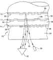
一种实施方案包括用作光学数据存储介质的多层金属/衬底组合。图1显示了一种实施方案,光学数据存储系统10。光学存储介质12包括透明衬底14和在第一数据凹坑图案19上的高反射薄膜层或涂层20。光学激光30向介质12发射光束,如图1所示。通过薄膜层20反射的光束的光被检测器32感知,其根据薄膜层上特定点中有无凹坑或脊感知光强度的调整。这种盘是独特的,由于其下面存在的一种合金被沉积在信息凹坑和脊上,并用作高反射薄膜20。在一种替代方案(未示出)中,通过背对背连接两个光学存储介质12改变盘,也就是说,具有各自面向外的透明衬底14。One embodiment includes a multilayer metal/substrate combination for use as an optical data storage medium. FIG. 1 shows one embodiment, an optical
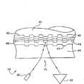
图2中示出了另一实施方案,光学数据存储系统110。光学存储介质112包括透明衬底114,和高反射薄膜层120,在染料层122上方,染料层122放置在第一图案119上。光学激光130向介质112发射光束,如图2所示。如前所述,通过用激光使部分染料层变形将数据存放在盘上。然后,用来自光束的光播放盘,光束通过薄膜层120反射并被检测器132感知。检测器132根据染料层中有无变形感知光强度的调整。这种盘是独特的,由于其下面存在的一种合金被沉积在染料层122上,并用作高反射薄膜或涂层120。在一种替代方案(未示出)中,通过背对背连接两种光学存储介质112改变盘,也就是说,具有各自面向外的透明衬底114。Another embodiment, an optical
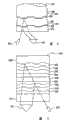
图3示出了另一种实施方案,光学数据存储系统210。光学存储介质212包括透明衬底214,在第一数据凹坑图案215上的部分反射薄膜层或涂层216,透明隔层218,和在第二数据凹坑图案219上的高反射薄膜层或涂层220。光学激光230向介质212发射光束,如图3所示。通过薄膜层216或220反射的光束的光被检测器232感知,其根据薄膜层上特定点中有无凹坑感知光强度的调整。这种盘是独特的,由于其下面存在的一种合金被沉积在信息凹坑和脊上,并用作高反射薄膜220或半反射层216。在另一种替代方案(未示出)中,通过背对背连接两种光学存储介质212改变盘,也就是说,具有各自面向外的透明衬底214。连接方法可为UV固化粘合剂、热熔粘合剂或其它类型的粘合剂。FIG. 3 shows another embodiment, an optical
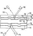
图4中示出了另一实施方案,为光学数据存储系统310。光学存储介质312包括透明衬底314,在第一数据凹坑图案315上的部分反射薄膜层或涂层316或层“0”,透明隔层318,在第二数据凹坑图案319上的另一部分反射薄膜层或涂层320或层“1”,第二透明隔层322,和在第三凹坑图案323上的高反射薄膜层或涂层324或层“2”。光学激光330向介质312发射光束,如图4所示。通过薄膜层316、320或324反射的光束的光被检测器332感知,其根据薄膜层上特定点中有无凹坑感知光强度的调整。这种盘是独特的,由于其下面存在的任意或全部合金被沉积在信息凹坑和脊上,并用作高反射薄膜或涂层324或半反射层或涂层316和320。为了回放层2上的信息,来自激光二极管330的光束透过透明聚碳酸酯衬底,经过第一半反射层0和第二半反射层1,然后从层2反射回到检测器332。在另一种替代方案(未示出)中,可通过背对背连接两种光学存储介质312改变盘,也就是说,具有各自面向外的透明衬底314。连接方法可为UV固化粘合剂、热熔粘合剂或其它类型的粘合剂。Another embodiment is shown in FIG. 4 as an optical
图5显示了又一实施方案,为光学数据存储系统410。光学存储介质412包括透明衬底或透明层414,在第一数据凹坑图案415上的介电层416,由具有微结构的材料制成并包括能重复经历激光引发的从第一状态到第二状态转变且复原的区域或部分的记录层418(即光学可再记录或可再写层),如相变材料或磁-光材料,另一介电材料420,高反射薄膜层422,和透明衬底或层424。本说明书中使用的介电材料是一种电绝缘体或其中电场可在最小功率耗散下被维持的材料。光学存储介质410的不同层414、416、418、420和422优选被定向以便彼此邻近。FIG. 5 shows yet another embodiment, an optical
记录层418的常用相变材料包括锗-锑-碲(Ge-Sb-Te)、银-铟-锑-碲(Ag-In-Sb-Te)、铬-锗-锑-碲(Cr-Ge-Sb-Te)等。介电层416或420的常用材料包括硫化锌-二氧化硅化合物(ZnS·SiO2)、氮化硅(SiN)、氮化铝(AlN)等。记录层418的常用磁-光材料包括铽-铁-钴(Tb-Fe-Co)或钆-铽-铁(Gd-Tb-Fe)。光学激光430向介质412发射光束,如图5所示。在相变可记录光学介质的记录模式中,根据输入数字数据调整或打开和关闭光束的光,并用合适的物镜聚焦到记录层418上,同时以合适的速度旋转介质以在记录层中实现微结构或相变。在回放模式中,通过介质412被薄膜层422反射的光束的光被检测器432感知,其根据记录层中特定点的结晶或非晶状态感知光强度的调整。这种盘是独特的,由于其下面存在的一种合金被沉积在介质上,并用作高反射薄膜422。在另一种替代方案(未示出)中,可通过背对背连接两种光学存储介质412改变盘,也就是说,具有各自面向外的透明衬底或涂层414。连接方法可为UV固化粘合剂、热熔粘合剂或其它类型的粘合剂。Commonly used phase change materials for the
如图5所示,如果透明衬底414的厚度为约1.2mm厚,由注射成型的聚碳酸酯制成,并具有连续螺旋形的凹槽和脊,424为UV固化的丙烯酸树脂,厚度为3-15微米,用作保护层,回放激光430在780-820纳米处,且可再写层418为典型组合物的相变材料如Ag-In-Sb-Te,则它就是压缩盘-可再写盘的结构,或一般称为CD-RW。为了记录和读取信息,相变盘利用记录层从低反射率(暗)的非晶相变到高反射率(亮)的结晶相的能力。在记录前,相变层处于结晶状态。在记录过程中,聚焦到记录层上的高功率激光束将加热相变材料至高温,且当关闭激光时,被加热的点非常快地冷却形成非晶状态。这样就根据将聚焦激光束打开和关闭的输入数据形成一系列的非晶状态的暗点。这些开和关对应于数字数据流的“0”和“1”。As shown in FIG. 5, if the
读取时,使用低激光功率聚焦并沿盘的轨道读取暗或亮点以回放记录的信息。为了擦除,使用中等激光功率聚焦到凹槽或轨道上,同时盘旋转,从而聚焦的点达到中间温度。在激光点移动到另一位置后,点冷却至室温,并具有反射率高的结晶结构。这使记录层回复到其最初或擦除状态。点从非晶到结晶状态的转变是完全可逆的,因此可实现多次记录和擦除循环,并可没有困难地重复记录和读回不同的数据。When reading, use low laser power to focus and read dark or bright spots along the track of the disc to playback the recorded information. For erasing, a moderate laser power is used to focus onto the groove or track while the disc rotates so that the focused spot reaches an intermediate temperature. After the laser spot is moved to another location, the spot cools to room temperature and has a highly reflective crystalline structure. This returns the recording layer to its original or erased state. The transition of the dots from the amorphous to the crystalline state is fully reversible, so multiple write and erase cycles are possible, and different data can be repeatedly recorded and read back without difficulty.
如果透明衬底414的厚度为约0.5-0.6mm厚,由注射成型的聚碳酸酯制成,并具有连续螺旋形的凹槽和脊,416和420为一般由ZnS.SiO2制成的介电层,且418由相变材料如Ag-In-Sb-Te或Ge-Sb-Te制成,422由本文公开的银合金制成,424为粘合具有相同结构的另一半的UV固化树脂,如图5所示,读和写激光430在630-650纳米波长处,那么它为具有可再写能力的数字通用盘,或一般称为DVD+RW。一些优选的可相变材料(phase-changeable material)包括以下系列的材料:As-Te-Ge、As-In-Sb-Te、Te-Ge-Sn、Te-Ge-Sn-O、Te-Se、Sn-Te-Se、Te-Ge-Sn-Au、Ge-Sb-Te、Sb-Te-Se、In-Se-Tl、In-Sb、In-Sb-Se、In-Se-Tl-Co、Cr-Ge-Sb-Te和Si-Te-Sn,其中As为砷,Te为碲,Ge为锗,Sn为锡,O为氧,Se为硒,Au为金,Sb为锑,In为铟,Tl为铊,Co为钴,和Cr为铬。在这种盘构造中,高反射层422不仅需要650纳米波长处的高反射率和高热导率,而且需要对ZnS·SiO2的高耐腐蚀性。常规铝合金没有足够高的反射率,也没有足够高的热导率。纯银或其它常规银合金没有高的耐腐蚀性,也没有高反射率和高热导率。因此,另一实施方案提供一系列能满足这一应用要求的银合金。If the
图6显示了另一种实施方案,为可再写型光学信息存储系统510。透明覆层514为大约0.1mm厚。介电层516和520优选由ZnS·SiO2制成,并用作可再写层或相变层518的保护层。可再写层518优选由Ag-In-Sb-Te等形成。高反射层522优选由银合金形成,如本文公开的银合金。透明衬底524优选大约1.1mm厚,具有连续螺旋形凹槽和脊轨道,通常由聚碳酸酯树脂制成。激光530优选具有约400nm的波长,具有将激光束聚焦到记录层518上的联合光学装置。反射的激光束被检测器532接收,其优选包括关联数据处理能力以读回记录的信息。该系统510有时称为“数字图像记录系统”或DVR设计用来记录高清晰度的TV信号。该光学信息存储系统510的操作原理与CD-RW盘大致相同,除了记录密度高得多,其5英寸直径盘的存储容量为大约20千兆字节。再者,磁盘组的性能依赖于400nm波长的高反射层522,其具有高耐腐蚀性和非常高的热导率。常规反射层如铝、金或铜均难于满足这种要求。因此,另一实施方案是提供能满足这些高要求的银合金反射层。FIG. 6 shows another embodiment, a rewritable optical
可用于实施本发明的其它光学记录介质包括例如从设备两面可读的光学存储设备,和在一些实施方案中还从设备两面可再写的光学存储设备。Other optical recording media that may be used to practice the invention include, for example, optical storage devices that are readable from both sides of the device, and in some embodiments also rewritable from both sides of the device.
图7中图示了一种实施方案,为光学数据存储系统610。光学存储系统610有时称为DVD-14,并说明了具有在结构两面存储可访问数据的能力的设备。One embodiment is illustrated in FIG. 7 as an optical
光学存储系统610包括0.6mm厚透明聚碳酸酯衬底(PC),邻近PC层或PC层的一部分是包括一系列凹坑和脊的第一数据凹坑图案614。邻近层614并与层614轮廓一致的是半反射层或涂层618。邻近层或涂层618的是由透明材料组成的隔层622,邻近隔层622或隔层622的一部分是包括一系列凹坑和脊的第二数据凹坑图案626。邻近并与第二数据凹坑图案626轮廓一致的是反射层或涂层630。半发射层或涂层618和高反射层630都可从结构610的同一面读出。The
邻近层或涂层634是第二反射层或涂层638。层或涂层638邻近并与包括一系列凹坑和脊的第三数据凹坑图案642的轮廓一致。第三数据凹坑图案642和高反射层或涂层638从设备的一面可读,该面与设备可读出数据凹坑图案618、626的另一面相反。邻近或包括数据凹坑图案642的是第二0.6mm厚的聚碳酸酯层。Adjacent layer or
光学激光660向第二聚碳酸酯层PC发射光束,光束被高反射层或涂层638反射,并被检测器662根据高反射涂层或层上的特定点中有无凹坑来感知光强度的调整。An
如图7所示,从设备610与激光660相反的面将来自激光650的第二光束引向第一聚碳酸酯衬底层PC,并向着数据凹坑图案614。如图7所示,第二激光650向半反射层或涂层618和高反射层630发射光束。激光650发射出的至少光束的一部分通过半反射层618到达反射层626。层或涂层626反射的光束的光被检测器652感知,其根据高反射层上的特定点中有无凹坑或脊感知光强度的调整。As shown in FIG. 7 , a second beam from
尽管图7中示出的光学存储设备包括多个激光源650、660和多个检测器652、662,但这可使用配置的单个激光源和检测器实现,从而可使用同一光束源和检测器收集来自所有信息凹坑和脊组包括设备的信号,例如组618、626、642。Although the optical storage device shown in FIG. 7 includes
又一实施方案是如图8所示的光学存储系统710。光学存储介质710说明了DVD-18,并代表具有从光学存储介质两面可读的多个信息层的光学存储系统。Yet another embodiment is an
光学存储系统710包括0.6mm厚的透明衬底712,其邻近或包括第一数据凹坑图案714。数据凹坑图案714包括一系列凹坑和脊,并邻近半反射层或涂层716。设备还包括约50微米厚的透明隔层718,和邻近高反射薄膜或涂层722的第二数据凹坑图案720。半反射层或涂层716和高反射层或涂层722都可从710的同一面读出。The
光学激光770向透明层712发射光束。如图8所示,激光源770发射的至少光束的一部分通过半反射层716到达高反射层722。半反射层或涂层716和高反射层722反射的光束的光被检测器772感知,其根据高反射层或半反射层上的特定点中有无凹坑或脊感知光强度的调整。
图8所示的光学存储设备还包括隔层724,其连接包括第一二信息层714、720的设备部分与包括第三和第四信息层728、734的设备部分。衬底层724邻近并隔开高反射层或涂层728和高反射层或涂层722。The optical storage device shown in FIG. 8 also includes a
高反射层或涂层724邻近并与凹坑和脊或数据凹坑图案层728的轮廓一致。层728邻近隔层726,隔层726邻近半反射层732,半反射层732邻近并与数据凹坑图案层734的轮廓一致。数据凹坑图案层734邻接或邻近0.6mm厚的衬底层736。A highly reflective layer or
在图8所示的实施方案中,提供任选的第二光学激光780,其向层736发射光束。激光780发射的部分光通过半反射层或涂层732,并被高反射层或涂层724反射,半反射层或涂层732和高反射层724反射的光被检测器782感知,其根据高反射层上的特定点中有无凹坑或脊感知光强度的调整。In the embodiment shown in FIG. 8 , an optional second
尽管图8所示的光学存储设备包括多个激光源770、780和多个检测器752、772,但这可使用配置的单个激光源和检测器实现,从而可使用同一光束源和检测器收集所有信息凹坑和脊组包括设备的信号。Although the optical storage device shown in FIG. 8 includes
又一实施方案包括提出的有时称为“Blu-ray”的下一代光学存储设备。Blu-ray设备结合了在405nm波长下操作的激光和数值孔径为0.85的透镜。Yet another embodiment includes a proposed next-generation optical storage device sometimes referred to as "Blu-ray." Blu-ray devices combine a laser operating at a wavelength of 405nm and a lens with a numerical aperture of 0.85.
如图9所示,预录型“Blu-Ray”盘的光学存储系统810包括从设备的相同面可读的两组信息凹坑和脊818和830。设备810包括厚度为约0.1mm的透明覆层814,和与高反射层或涂层834邻近的厚度为约1.1mm的衬底层838。高反射层或涂层834邻近并与注射成型到衬底838上的第二数据凹坑图案830一致。包括一组凹坑和脊的数据凹坑图案830邻近衬底838或其一部分。层826邻近半反射层822。半反射层或涂层822邻近并与包括一组凹坑和脊的第一数据凹坑图案818一致。数据凹坑818邻近透明覆层814或其一部分。As shown in Figure 9, an
如图9所示,提供光束源激光850,以及检测器852。光学激光850通过物镜(图9中未示出)向层814发射光束。激光850发射的部分光通过透镜(未示出)、半反射层或涂层822,并被高反射层或涂层834反射和被检测器852感知,其根据高反射层或涂层822上的特定点中有无凹坑或脊感知光强度的调整。As shown in Figure 9, a beam
激光850发射的光束的一部分部分被半反射层或涂层822反射,并被检测器852感知,其根据半反射层或涂层822上的特定点中有无凹坑或脊感知光强度的调整。A portion of the beam emitted by the
在一种实施方案中,如图10所示,Blu-ray可再写型光学存储设备910还包括两个读和可再写层926、954。光学存储设备910包括约1.1mm厚、邻近高反射层或涂层968的衬底层972。邻近层或涂层968的是包括ZnS-SiO2的第一介电层964,邻近层964的是第一界面层960如Ge-N或其它那些。邻近层960的是厚度约10-15nm的相变型记录层如Ge-Sb-Te 954等,邻近层954的是层950,为第二层如Ge-N等。邻近层950是ZnS-SiO2的第二介电层一层946。In one embodiment, as shown in FIG. 10, a Blu-ray rewritable
光学存储设备910还包括夹在大约20-40微米厚的介电层946和约10nm厚的半反射层或涂层938之间的中间层942。由ZnS-SiO2组成的第三介电层934邻近层或涂层938。邻近层934是用Ge-N或其它制成的第三界面层930,由Ge-Sn-Sb-Te或其它相变材料组成的6-10nm厚的记录层926夹在层930和Ge-N等制成的第四界面层922之间。邻近层922是第四层由ZnS-SiO2组成的介电材料层918。邻近层918是约80-100微米厚的透明覆层914。The
如图10所示,激光970发射的光束通过层914、918、922、926、930、934,并被层938反射和被检测器972感知。激光970发射光束的一部分通过层914、918、922、926、930、934、938、942、946、950、954、960、964,并被层968反射,射向且被检测器972感知。所有公开的银合金组合物都可用于半反射层938或高反射层968。在记录模式中,激光970的激光束将被聚焦到相变层926或954上以改变其反射性质,类似于常规的CD-RW、DVD-RW、DVD+RW,或在现有技术如美国专利6544616、6652948、6649241和其它中公开的回放激光波长约400nm的下一代压缩盘。As shown in FIG. 10 , the beam emitted by
应认识到图11所示的盘结构可被改进,使1014和1060都大约具有相同的厚度或约0.6mm,并具有类似的相变材料记录组,盘结构可为“高级压缩盘”或AOD型可再写压缩盘,其中记录和回放激光波长为约400nm。It should be recognized that the disc structure shown in Figure 11 could be modified so that both 1014 and 1060 are about the same thickness or about 0.6 mm, and have a similar phase change material recording set, the disc structure could be an "Advanced Compact Disc" or AOD type rewritable compact disc in which the recording and playback laser wavelength is about 400nm.
还应认识到图7、8、9、12中所示的所有压缩盘结构都包含预录型双层盘结构,其中回放激光束具有约635-650nm的波长,如图7和8,或包含双层HD-DVD盘结构,其中回放激光具有约400nm的波长,或包含两层或多层信息都从盘一面记录或回放的任何其它压缩盘结构,其中利用本发明公开的银合金的半反射层。It should also be recognized that all of the compact disc structures shown in Figures 7, 8, 9, 12 include pre-recorded dual-layer disc structures in which the playback laser beam has a wavelength of about 635-650 nm, as in Figures 7 and 8, or include Dual-layer HD-DVD disc structure, wherein the playback laser has a wavelength of about 400 nm, or any other compact disc structure comprising two or more layers of information recorded or played back from one side of the disc, wherein the semi-reflective properties of the disclosed silver alloys are utilized layer.
图11所示的一种实施方案为还包括两个一次性写入层1048和1024的‘Blu-ray’构造的光学存储设备1010。光学存储设备1010为由1.1mm厚衬底层1060组成的双层一次性写入记录介质,衬底层1060邻近约30-60nm厚通常用本发明的银合金或铝合金制成的高反射层1056。层1056邻近保护层1052,层1052邻近15-25nm厚并由Te-O-Pd基材料或其它材料组成的可记录层1048。层1048邻近保护薄膜层1044。One embodiment shown in FIG. 11 is an
层1044邻近分离层或隔层1040,其邻近10nm厚的由本发明的银合金制成的半反射层或涂层1034。层或涂层1034邻近保护薄膜层1030,其邻近第二个10nm厚的包括Te-O-Pd基材料或其它材料的记录层1024。层1024邻近保护薄膜1020,其邻近0.075mm厚的覆层1014。
如图11所示,激光1070发射的光束通过图11中NA为0.85的透镜系统(未示出),经过层1014、1020、1024、1030,并被半反射层1034反射和检测器1072感知。激光1070发射光束的一部分通过层1014、1020、1024、1030、1034、1040、1044、1048、1052,并被高反射层1056反射和检测器1072感知。检测器1072根据半反射层或涂层1034和高反射层1056上的特定点中层1024或1048的非晶或结晶状态感知光强度的调整,并通过将1070激光的激光聚焦到一次性写入层1024或1048上来读回存储的信息。隔层1040应足够厚,以便当读取光束聚焦到可记录层1024上时,读取光束能被充分散焦到下一可记录层1048上,并且只有来自1024的光信息的调整被反射回到检测器1072。相反,当读取光束聚焦到可记录层1048上时,读取光束被充分散焦到另一记录层1024上,并且只有来自1048的调整被反射到检测器1072和读取。As shown in FIG. 11 , the beam emitted by
还应认识到,如图10和11所示,可构造具有相变记录层或其它类型记录层的一次性写入或可再写型双层盘,以使至少两个记录层可从一面或盘的相同面记录和读取,其中可利用和使用由本发明的银合金制成的半反射层。It should also be recognized that, as shown in FIGS. 10 and 11 , write-once or rewritable dual-layer discs with phase change recording layers or other types of recording layers can be constructed so that at least two recording layers can be changed from one side or the other. The same side of the disc records and reads where a semi-reflective layer made of the silver alloy of the present invention can be utilized and used.
如图12所示的另一实施方案为预录型光学存储设备1110,其为提出的有时称为高级光学设备(AOD)的下一代光学存储设备。AOD为使用405nm波长激光束和NA为0.65的透镜系统记录和检索光学存储设备两个面信息的系统,其中一般用注射成型的聚碳酸酯制成的透明衬底1120和1140为大约0.6mm厚。Another embodiment, as shown in Figure 12, is a pre-recorded
设备1110包括邻近高反射层或涂层1136的透明衬底层1140,其邻近并与包括一组凹坑和脊的第一数据凹坑图案1138的轮廓一致。高反射层1136邻近隔层1132,隔层1132邻近本发明的半反射层或涂层1124,层或涂层1124邻近并与包括一组凹坑和脊的第二数据凹坑图案1128的轮廓一致。层1124邻近第二衬底或层1120。The
如图12所示,激光1150发射的光束的一部分通过层1120、1124、1128、1132,并被高反射层1136反射和检测器1152感知。激光1150发射的光束的一部分通过层1120,并被半反射层或涂层1124反射和检测器1152感知。检测器1152通过聚焦到层1124或1136上并根据半反射层或涂层1124和高反射层或涂层1136上的特定点中有无凹坑或脊感知光强度的调整。As shown in FIG. 12 , a portion of the beam emitted by
在图13所示的另一实施方案中,有机染料可记录双层型光学存储设备1210包括从设备的同一面既可读又可记录的两个层。设备1210包括邻近第一可记录染料层1218的透明衬底层1214。染料层1218邻近本发明的半反射层或涂层1222。层或涂层1222,有时称为“层0”或L0,邻近隔层1226。隔层1226邻近第二染料记录层1230。层1230邻近高反射层或涂层1234。反射层或涂层1234,有时称为“层1”或L1,邻近聚碳酸酯衬底或层1238。In another embodiment shown in FIG. 13, an organic dye-recordable dual-layer
在写模式中,如图13所示,光束源1250发射通过层1214的激光束,并被聚焦到染料层1218上。当激光1250在高强度下操作时,聚焦在层1218上的光束使层1218中的染料分解,形成包括等价于一系列凹坑和脊的数据凹坑图案。激光1250发射的光束的一部分通过层1214、1218、1222、1226,并被聚焦到染料层1230上。当激光1250在高强度下操作时,聚焦到层1230上的光束使层1230中的染料分解,形成包括一系列凹坑和脊的数据凹坑图案。In the write mode, as shown in FIG. 13 ,
在读模式中,激光1250发射的光束的一部分通过透明聚碳酸酯层1214和染料层1218,被半反射层或涂层1222反射和检测器1252感知。光束的一部分还通过层1214、1218、1222、1226、1230,并被高反射层1234反射和检测器1252感知。检测器1252根据反射层或涂层1234上的特定点中有无凹坑或脊,或通过半发射层或涂层1222根据激光1250是否聚焦到半反射层1222或高反射层1234上来感知光强度的调整。对于有机染料基光学记录介质的通用操作,读者可参考美国专利6641889、6551682等。In read mode, a portion of the beam emitted by
还应认识到,图13所示的压缩盘结构可为双层DVD-R或DVD+R盘,其中回放激光束具有约635-650nm的波长,或结构可为双层HD-DVD-R盘,其中回放激光具有约400nm的波长,或任何其它压缩盘结构,其中两个或多个层信息可全部从盘的一面记录或回放,其中使用本发明公开的银合金的半反射层或层。It should also be appreciated that the compact disc structure shown in Figure 13 may be a dual layer DVD-R or DVD+R disc, where the playback laser beam has a wavelength of about 635-650 nm, or the structure may be a dual layer HD-DVD-R disc , where the playback laser has a wavelength of about 400nm, or any other compact disc structure where two or more layers of information can be recorded or played back all from one side of the disc, using a semi-reflective layer or layer of silver alloy as disclosed herein.
本文使用的术语“反射率”是指入射到透明衬底14、114、214、314、414或514上、并当聚焦到层20、120、216、220、316、320、324、422或522区域上的点时,基本上可被光学读出设备中的光检测器感知的光强度的分数。假设读出设备包括激光、适当设计的光路和光检测器,或它们的功能等价物。As used herein, the term "reflectivity" refers to the reflection rate incident on a
本发明基于这种观察,即特定的银基合金提供足够的反射率和耐腐蚀性,以用作光学存储介质中的高反射或半反射层,没有金基合金的固有成本或硅基材料的工艺复杂性。在一种实施方案中,银与相对少量的锌形成合金。在这种实施方案中,锌和银数量之间的关系为从约0.01a/o%(原子百分数)到约15a/o%的锌和从约85a/o%到约99.99a/o%的银。但对于每种金属,优选合金具有约0.1a/o%到约10.0a/o%的锌和从约90.0a/o%到约99.9a/o%的银。The present invention is based on the observation that certain silver-based alloys provide sufficient reflectivity and corrosion resistance to be used as highly reflective or semi-reflective layers in optical storage media without the inherent cost of gold-based alloys or the cost of silicon-based materials. Process complexity. In one embodiment, silver is alloyed with a relatively small amount of zinc. In this embodiment, the relationship between the amount of zinc and silver is from about 0.01a/o% (atomic percent) to about 15a/o% zinc and from about 85a/o% to about 99.99a/o% silver. However, for each metal, preferred alloys have from about 0.1 a/o% to about 10.0 a/o% zinc and from about 90.0 a/o% to about 99.9 a/o% silver.
在另一实施方案中,银与相对少量的铝形成合金。在这种实施方案中,铝和银数量之间的关系为从约0.01a/o%(原子百分数)到约5a/o%的铝和从约95a/o%到约99.99a/o%的银。但对于每种金属,优选合金具有约0.1a/o%到约3.0a/o%的铝和从约97a/o%到约99.9a/o%的银。In another embodiment, silver is alloyed with a relatively small amount of aluminum. In this embodiment, the relationship between the amounts of aluminum and silver is from about 0.01 a/o% (atomic percent) to about 5 a/o % of aluminum and from about 95 a/o % to about 99.99 a/o % silver. However, for each metal, preferred alloys have from about 0.1 a/o% to about 3.0 a/o% aluminum and from about 97a/o% to about 99.9a/o% silver.
在另一实施方案中,如上所述的银基二元合金体系还与镉(Cd)、锂(Li)或锰(Mn)形成合金。如果这些金属中的一种或多种取代合金中的部分银,则得到的薄膜的耐腐蚀性可能增加;但是,反射率也可能降低。可有利地取代二元合金中部分银的镉、锂或锰量,对于镉来说,为存在银量的约0.01a/o%到约20a/o%,对于锂来说,为存在银量的约0.01a/o%到约10a/o%或甚至到约15a/o%,对于锰来说,为存在银量的约0.01a/o%到约7.5a/o%。In another embodiment, the silver-based binary alloy system described above is also alloyed with cadmium (Cd), lithium (Li), or manganese (Mn). If one or more of these metals replaces some of the silver in the alloy, the corrosion resistance of the resulting film may increase; however, the reflectivity may also decrease. An amount of cadmium, lithium or manganese that may advantageously replace part of the silver in the binary alloy, for cadmium from about 0.01 a/o% to about 20 a/o% of the amount of silver present, for lithium the amount of silver present From about 0.01a/o% to about 10a/o% or even to about 15a/o% of manganese, from about 0.01a/o% to about 7.5a/o% of the amount of silver present.
在又一实施方案中,如上所述的银基锌和铝二元合金体系还与贵金属如金(Au)、铑(Rh)、铜(Cu)、钌(Ru)、锇(Os)、铱(Ir)、铂(Pt)、钯(Pd)和它们的混合物形成合金,贵金属可被加入到上述二元合金中,优选贵金属范围为存在银量的约0.01a/o-5.0a/o%。除了贵金属外,上述合金还可再与金属如钛(Ti)、镍(Ni)、铟(In)、铬(Cr)、锗(Ge)、锡(Sn)、锑(Sb)、镓(Ga)、硅(Si)、硼(B)、锆(Zr)、钼(Mo)和它们的混合物形成合金。相对于上述银合金体系中存在的银量,这些金属优选加入的量为存在银量的约0.01a/o%到约5.0a/o%。In yet another embodiment, the silver-based zinc and aluminum binary alloy system described above is also combined with noble metals such as gold (Au), rhodium (Rh), copper (Cu), ruthenium (Ru), osmium (Os), iridium (Ir), platinum (Pt), palladium (Pd) and mixtures thereof form alloys, noble metals may be added to the above binary alloys, preferably noble metals in the range of about 0.01 a/o - 5.0 a/o % of the amount of silver present . In addition to noble metals, the above alloys can be combined with metals such as titanium (Ti), nickel (Ni), indium (In), chromium (Cr), germanium (Ge), tin (Sn), antimony (Sb), gallium (Ga ), silicon (Si), boron (B), zirconium (Zr), molybdenum (Mo) and their mixtures form alloys. These metals are preferably added in amounts ranging from about 0.01 a/o % to about 5.0 a/o % of the amount of silver present relative to the amount of silver present in the silver alloy systems described above.
在又一实施方案中,银与相对少量的锌和铝两者形成合金。在这种实施方案中,锌、铝和银量之间的关系为约0.1a/o%到约15a/o%的锌、约0.1a/o%到约5a/o%的铝和约80a/o%到约99.8a/o%的银。但对于每种金属,优选合金具有约0.1a/o%到约5.0a/o%的锌、约0.1a/o%到约3.0a/o%的铝和约92.0a/o%到约99.8a/o%的银。In yet another embodiment, silver is alloyed with relatively small amounts of both zinc and aluminum. In this embodiment, the relationship between the amounts of zinc, aluminum and silver is about 0.1 a/o % to about 15 a/o % of zinc, about 0.1 a/o % to about 5 a/o % of aluminum and about 80 a/o % o% to about 99.8a/o% silver. However, for each metal, preferred alloys have from about 0.1 a/o% to about 5.0 a/o% zinc, from about 0.1 a/o% to about 3.0a/o% aluminum, and from about 92.0a/o% to about 99.8a /o% silver.
在还一实施方案中,如上所述的银基锌-铝三元合金体系还与第四种金属形成合金。第四种金属可包括锰或镍。如果这些金属中的一种或混合物取代合金中的部分银,则得到的薄膜的耐腐蚀性可能增加;但是,反射率也可能降低。可有利地取代上述三元合金中部分银的锰或镍量,对于锰来说,为存在银量的约0.01a/o%到约7.5a/o%,优选范围在存在银量的约0.01a/o%和约5.0a/o%之间。镍量可在存在银量的约0.01a/o%和约5.0a/o%之间,优选范围在存在银量的约0.01a/o%和约3.0a/o%之间。In yet another embodiment, the silver-based zinc-aluminum ternary alloy system described above is also alloyed with a fourth metal. The fourth metal may include manganese or nickel. If one or a mixture of these metals replaces some of the silver in the alloy, the corrosion resistance of the resulting film may increase; however, the reflectivity may also decrease. The amount of manganese or nickel that can advantageously replace part of the silver in the above ternary alloys is, for manganese, from about 0.01 a/o % to about 7.5 a/o % of the amount of silver present, preferably in the range of about 0.01 a/o % of the amount of silver present Between a/o % and about 5.0 a/o %. The amount of nickel may be between about 0.01 a/o % and about 5.0 a/o % of the amount of silver present, and preferably ranges between about 0.01 a/o % and about 3.0 a/o % of the amount of silver present.
在又一实施方案中,如上所述的银基锌-铝三元合金体系还与贵金属如金、铑、铜、钌、锇、铱、铂、钯和它们的混合物形成合金,贵金属可被加入到上述三元合金中,优选贵金属范围为存在银量的约0.01a/o-5.0a/o%。除了贵金属外,上述合金还可与金属如钛、镍、铟、铬、锗、锡、锑、镓、硅、硼、锆、钼和它们的混合物形成合金。相对于上述银合金体系中存在的银量,这些金属优选加入的量为存在银量的约0.01a/o%到约5.0a/o%。In yet another embodiment, the silver-based zinc-aluminum ternary alloy system described above is also alloyed with noble metals such as gold, rhodium, copper, ruthenium, osmium, iridium, platinum, palladium and mixtures thereof, the noble metals can be added Into the above ternary alloys, the preferred noble metal range is from about 0.01 a/o to 5.0 a/o % of the amount of silver present. In addition to noble metals, the above alloys can be alloyed with metals such as titanium, nickel, indium, chromium, germanium, tin, antimony, gallium, silicon, boron, zirconium, molybdenum, and mixtures thereof. These metals are preferably added in amounts ranging from about 0.01 a/o % to about 5.0 a/o % of the amount of silver present relative to the amount of silver present in the silver alloy systems described above.
在另一实施方案中,光学存储介质包括在至少一个主表面中具有特征图案的第一衬底和邻近特征图案的第一反射层。反射层由银和锌合金制成,其中银量和锌量之间的关系用AgxZny限定,其中0.85<x<0.9999和0.0001<y<0.15。In another embodiment, an optical storage medium includes a first substrate having a pattern of features in at least one major surface and a first reflective layer adjacent to the pattern of features. The reflective layer is made of silver and zinc alloy, where the relationship between the amount of silver and the amount of zinc is defined by Agx Zny , where 0.85<x<0.9999 and 0.0001<y<0.15.
在另一实施方案中,光学存储介质包括在至少一个主表面中具有特征图案的第一衬底和邻近特征图案的第一反射层。反射层由银和铝合金制成,其中银量和铝量之间的关系用AgxAlz限定,其中0.95<x<0.9999和0.0001<z<0.05。In another embodiment, an optical storage medium includes a first substrate having a pattern of features in at least one major surface and a first reflective layer adjacent to the pattern of features. The reflective layer is made of silver and aluminum alloy, where the relationship between the amount of silver and aluminum is defined by Agx Alz , where 0.95<x<0.9999 and 0.0001<z<0.05.
在另一实施方案中,光学存储介质包括在至少一个主表面中具有特征图案的第一衬底和邻近特征图案的第一反射层。反射层由银和锌和铝合金制成,其中银量和锌量和铝量之间的关系用AgxZnyAlz限定,其中0.80<x<0.998和0.001<y<0.15,和0.001<z<0.05。In another embodiment, an optical storage medium includes a first substrate having a pattern of features in at least one major surface and a first reflective layer adjacent to the pattern of features. The reflective layer is made of silver and zinc and aluminum alloy, where the relationship between the amount of silver and the amount of zinc and aluminum is defined by Agx Zny Alz , where 0.80<x<0.998 and 0.001<y<0.15, and 0.001<z<0.05.
在另一实施方案中,光学存储介质包括在至少一个主表面中具有特征图案的第一衬底和邻近特征图案的第一反射层。反射层由银和锰合金制成,其中银和锰量之间的关系用AgxMnt限定,其中0.925<x<0.9999和0.0001<t<0.075。In another embodiment, an optical storage medium includes a first substrate having a pattern of features in at least one major surface and a first reflective layer adjacent to the pattern of features. The reflective layer is made of silver and manganese alloy, where the relationship between the amount of silver and manganese is defined by Agx Mnt , where 0.925<x<0.9999 and 0.0001<t<0.075.
在另一实施方案中,光学存储介质包括在至少一个主表面中具有特征图案的第一衬底和邻近特征图案的第一反射层。反射层由银和锗合金制成,其中银量和锗量之间的关系用AgxGeq限定,其中0.97<x<0.9999和0.0001<q<0.03。In another embodiment, an optical storage medium includes a first substrate having a pattern of features in at least one major surface and a first reflective layer adjacent to the pattern of features. The reflective layer is made of silver and germanium alloy, where the relationship between the amount of silver and germanium is defined by Agx Geq , where 0.97<x<0.9999 and 0.0001<q<0.03.
在另一实施方案中,光学存储介质包括在至少一个主表面中具有特征图案的第一衬底和邻近特征图案的第一反射层。反射层由银和铜和锰合金制成,其中银量和铜量和锰量之间的关系用AgxCupMnt限定,其中0.825<x<0.9998和0.0001<p<0.10,和0.0001<t<0.075。In another embodiment, an optical storage medium includes a first substrate having a pattern of features in at least one major surface and a first reflective layer adjacent to the pattern of features. The reflective layer is made of silver and copper and manganese alloy, where the relationship between the amount of silver and the amount of copper and manganese is defined by Agx Cup Mnt , where 0.825<x<0.9998 and 0.0001<p<0.10, and 0.0001<t<0.075.
在另一实施方案中,银与相对少量的锰形成合金。在这种实施方案中,锰和银量之间的关系为约0.01a/o%至约7.5a/o%的锰和约92.5a/o%至约99.99a/o%的银。但对于每种金属,优选合金具有约0.1a/o%至约5a/o%的锰和约95a/o%至约99.9a/o%的银。In another embodiment, silver is alloyed with relatively small amounts of manganese. In such embodiments, the relationship between the amount of manganese and silver is from about 0.01 a/o % to about 7.5 a/o % manganese and from about 92.5 a/o % to about 99.99 a/o % silver. However, preferred alloys have from about 0.1 a/o% to about 5 a/o% manganese and from about 95 a/o% to about 99.9 a/o% silver for each metal.
在又一实施方案中,如上所述的银基二元锰合金还与第三种金属形成合金。第三种金属可包括镉、镍、锂和它们的混合物。如果这些金属中的一种或混合物取代合金中的部分银,则得到的薄膜的耐腐蚀性可能增加;但是,反射率也可能降低。相对于上述二元合金体系中存在的银量,镉量可为合金的存在银量的约0.01a/o%到约20a/o%,镍量可为存在银量的约0.01a/o%到约5.0a/o%之间,锂量可为存在银量的约0.01a/o%到约10.0a/o%。In yet another embodiment, the silver-based binary manganese alloy described above is also alloyed with a third metal. The third metal may include cadmium, nickel, lithium and mixtures thereof. If one or a mixture of these metals replaces some of the silver in the alloy, the corrosion resistance of the resulting film may increase; however, the reflectivity may also decrease. Relative to the amount of silver present in the binary alloy system described above, the amount of cadmium may be from about 0.01 a/o percent to about 20 a/o percent of the amount of silver present in the alloy and the amount of nickel may be about 0.01 a/o percent of the amount of silver present The amount of lithium may be between about 0.01 a/o % and about 10.0 a/o % of the amount of silver present, between about 5.0 a/o %.
在又一实施方案中,如上所述的银基锰合金体系还与贵金属如金、铑、铜、钌、锇、铱、铂、钯和它们的混合物形成合金,贵金属可被加入到上述二元合金中,优选贵金属范围为存在银量的约0.01a/o-5.0a/o%。除了贵金属外,上述合金还可与金属如钛、铟、铬、锗、锡、锑、镓、硅、硼、锆、钼和它们的混合物形成合金。相对于上述银合金体系中存在的银量,后面金属优选加入的量为存在银量的约0.01a/o%到约5.0a/o%。In yet another embodiment, the silver-based manganese alloy system described above is also alloyed with noble metals such as gold, rhodium, copper, ruthenium, osmium, iridium, platinum, palladium, and mixtures thereof, which can be added to the above binary In the alloy, the preferred noble metal range is from about 0.01 a/o to 5.0 a/o % of the amount of silver present. In addition to noble metals, the above alloys can be alloyed with metals such as titanium, indium, chromium, germanium, tin, antimony, gallium, silicon, boron, zirconium, molybdenum, and mixtures thereof. The latter metal is preferably added in an amount ranging from about 0.01 a/o % to about 5.0 a/o % of the amount of silver present relative to the amount of silver present in the silver alloy system described above.
在又一实施方案中,银与相对少量的锗形成合金。在这种实施方案中,锗和银量之间的关系为约0.01a/o%至约3.0a/o%的锗和约97.0a/o%至约99.99a/o%的银。但对于每种金属,优选合金具有约0.1a/o%至约1.5a/o%的锗和约98.5a/o%至约99.9a/o%的银。In yet another embodiment, silver is alloyed with a relatively small amount of germanium. In such an embodiment, the relationship between the amount of germanium and silver is from about 0.01 a/o% to about 3.0 a/o% germanium and from about 97.0 a/o% to about 99.99 a/o% silver. However, preferred alloys have about 0.1 a/o% to about 1.5 a/o% germanium and about 98.5 a/o% to about 99.9 a/o% silver for each metal.
在又一实施方案中,如上所述的银基锗合金体系还与第三种金属形成合金。第三种金属可包括锰或铝。如果这些金属中的一种或混合物取代合金中的部分银,则得到的薄膜的耐腐蚀性可能增加;但是,反射率也可能降低。相对于上述二元合金体系中存在的银量,锰量可为存在银量的约0.01a/o%到约7.5a/o%,铝量可为存在银量的约0.01a/o%到约5.0a/o%。In yet another embodiment, the silver-based germanium alloy system described above is also alloyed with a third metal. The third metal may include manganese or aluminum. If one or a mixture of these metals replaces some of the silver in the alloy, the corrosion resistance of the resulting film may increase; however, the reflectivity may also decrease. The amount of manganese may be from about 0.01 a/o % to about 7.5 a/o % of the amount of silver present and the amount of aluminum may be from about 0.01 a/o % to the amount of silver present relative to the amount of silver present in the above binary alloy systems About 5.0 a/o%.
在又一实施方案中,如上所述的银基锗合金体系还与贵金属如金、铑、铜、钌、锇、铱、铂、钯和它们的混合物形成合金,贵金属可被加入到上述二元合金中,优选贵金属范围为存在银量的约0.01a/o-5.0a/o%。除了贵金属外,上述合金还可与金属如锌、镉、锂、镍、钛、锆、铟、铬、锡、锑、镓、硅、硼、钼和它们的混合物形成合金。相对于上述银合金体系中存在的银量,这些金属优选加入的量为存在银量的约0.01a/o%到约5.0a/o%。In yet another embodiment, the silver-based germanium alloy system described above is also alloyed with noble metals such as gold, rhodium, copper, ruthenium, osmium, iridium, platinum, palladium, and mixtures thereof, which can be added to the above binary In the alloy, the preferred noble metal range is from about 0.01 a/o to 5.0 a/o % of the amount of silver present. In addition to noble metals, the above alloys can be alloyed with metals such as zinc, cadmium, lithium, nickel, titanium, zirconium, indium, chromium, tin, antimony, gallium, silicon, boron, molybdenum, and mixtures thereof. These metals are preferably added in amounts ranging from about 0.01 a/o % to about 5.0 a/o % of the amount of silver present relative to the amount of silver present in the silver alloy systems described above.
在又一实施方案中,银与相对少量的铜和锰两者形成合金。在这种实施方案中,铜、锰和银量之间的关系为约0.01a/o%到约10a/o%的铜、约0.01a/o%到约7.5a/o%的锰和约82.5a/o%到约99.98a/o%的银。但对于每种金属,优选合金包括约0.1a/o%到约5.0a/o%的铜、约0.1a/o%到约3.0a/o%的锰和约92.0a/o%到约99.8a/o%的银。In yet another embodiment, silver is alloyed with relatively small amounts of both copper and manganese. In this embodiment, the relationship between the amount of copper, manganese and silver is about 0.01a/o% to about 10a/o% copper, about 0.01a/o% to about 7.5a/o% manganese and about 82.5 a/o% to about 99.98a/o% silver. However, for each metal, preferred alloys include about 0.1 a/o % to about 5.0 a/o % copper, about 0.1 a/o % to about 3.0 a/o % manganese, and about 92.0 a/o % to about 99.8 a /o% silver.
在还一实施方案中,如上所述的银基铜-锰合金体系还与第四种金属形成合金。第四种金属如铝、钛、锆、镍、铟、铬、锗、锡、锑、镓、硅、硼、钼和它们的混合物。相对于上述银合金体系中存在的银量,优选加入的第四种金属的量为存在银量的约0.01a/o%到约5.0a/o%。In yet another embodiment, the silver-based copper-manganese alloy system described above is also alloyed with a fourth metal. A fourth metal such as aluminum, titanium, zirconium, nickel, indium, chromium, germanium, tin, antimony, gallium, silicon, boron, molybdenum and mixtures thereof. Preferably, the fourth metal is added in an amount of about 0.01 a/o% to about 5.0 a/o% of the amount of silver present relative to the amount of silver present in the silver alloy system described above.
下面的表I中显示了这些银合金作为DVD-9双层盘半反射层的厚度为8-12纳米的薄膜的光学性质。如转让给Matsushita Electric的美国专利5464619和转让给Sony的美国专利5726970所述,在图3和表I中所示的双层压缩盘结构中,图3中层“0”或216的反射率R0、从图3中盘外侧测得的层“1”或220的反射率R1′和层“0”的透射率T0之间的关系是R0=R1T02,其中R1是层“1”自身的反射率。当为了平衡信号和反射率而最优化层“0”厚度,并且层“1”为50-60纳米的常规铝合金时,各种银合金的平衡反射率显示于表I,其中R为在厚度60纳米或更高时在650纳米波长下可获得的薄膜反射率,如果用作层“1”或DVD-9的高反射率层或光学信息存储介质的任何其它高反射率应用。表中的所有组成为原子百分数。The optical properties of these silver alloys as thin films of 8-12 nm thick as semi-reflective layers of DVD-9 dual layer discs are shown in Table I below. As described in U.S. Patent No. 5,464,619 assigned to Matsushita Electric and U.S. Patent No. 5,726,970 assigned to Sony, in the dual-layer compact disk structure shown in Fig. 3 and Table I, the reflectance R of layer "0" or 216 in Fig.3 , the relationship between the reflectance R1 ' of layer "1" or 220 measured from the outside of the disc in Fig. 3 and the transmittance T0 of layer "0" is R0 =R1 T02 , where R1 is The reflectivity of layer "1" itself. When layer "0" thickness is optimized for the balance of signal and reflectivity, and layer "1" is a conventional aluminum alloy of 50-60 nm, the balanced reflectance of various silver alloys is shown in Table I, where R is the thickness at Film reflectance obtainable at a wavelength of 650 nm at 60 nm or greater if used as layer "1" or as a high reflectivity layer for DVD-9 or any other high reflectivity application for optical information storage media. All compositions in the table are in atomic percent.
表I:用各种银合金层0和典型铝合金层1的DVD-9双层盘的层0和层1的反射率对比。Table I: Comparison of layer 0 and layer 1 reflectance of DVD-9 dual layer discs with layer 0 of various silver alloys and layer 1 of a typical aluminum alloy.
在又一实施方案中,溅射靶和光学信息存储介质上的薄膜为加入相对少的铝作为合金元素的银合金。在这种实施方案中,银和铝量之间的关系为约0.01a/o%至约5.0a/o%的铝和约95.0a/o%至约99.99a/o%的银。但优选约0.1a/o%至约3.0a/o%的铝和约97.0a/o%至约99.9a/o%的银。这种银和铝二元合金还可与锌、镉、锂、锰、镍、钛和锆或这些金属的混合物形成合金。相对于上述银和铝二元合金中存在的银量,可优选加入的上述指定金属的量为银含量的0.01a/o%至约5.0a/o%。In yet another embodiment, the sputtering target and the film on the optical information storage medium are silver alloys with relatively little addition of aluminum as an alloying element. In such embodiments, the relationship between the amount of silver and aluminum is from about 0.01 a/o % to about 5.0 a/o % aluminum and from about 95.0 a/o % to about 99.99 a/o % silver. However, about 0.1 a/o % to about 3.0 a/o % aluminum and about 97.0 a/o % to about 99.9 a/o % silver are preferred. This silver and aluminum binary alloy can also be alloyed with zinc, cadmium, lithium, manganese, nickel, titanium and zirconium or mixtures of these metals. The metals specified above may preferably be added in an amount of 0.01 a/o % to about 5.0 a/o % of the silver content relative to the amount of silver present in the above silver and aluminum binary alloy.
为了方便读者,下面是银合金的一些组合,其中合金元素用它们的周期表符号标示,它们可优选与银形成合金:Ag+Zn、或Ag+Cd、或Ag+Li、或Ag+Al、或Ag+Ni、或Ag+Mn、或Ag+Ti、或Ag+Zr、或Ag+Pd+Zn、或Ag+Pt+Zn、或Ag+Pd+Mn、或Ag+Pt+Mn、或Ag+Zn+Li、或Ag+Pt+Li、或Ag+Li+Mn、或Ag+Li+Al、或Ag+Ti+Zn、或Ag+Zr+Ni、或Ag+Al+Ti、或Ag+Pd+Ti、或Ag+Pt+Ti、或Ag+Ni+Al、或Ag+Mn+Ti、或Ag+Zn+Zr、或Ag+Li+Zr、或Ag+Mn+Zn、或Ag+Mn+Cu、或Ag+Pd+Pt+Zn、或Ag+Pd+Zn+Mn、或Ag+Zn+Mn+Li、或Ag+Cd+Mn+Li、或Ag+Pt+Zn+Li、或Ag+Al+Ni+Zn、或Ag+Al+Ni+Ti、或Ag+Zr+Ti+Cd、或Ag+Zr+Ni+Li、或Ag+Zr+Ni+Al、或Ag+Pt+Al+Ni、或Ag+Pd+Zn+Al、或Ag+Zr+Zn+Ti、或Ag+Ti+Ni+Al。For the convenience of the reader, the following are some combinations of silver alloys, where the alloying elements are indicated by their periodic table symbols, which may be preferably alloyed with silver: Ag+Zn, or Ag+Cd, or Ag+Li, or Ag+Al, Or Ag+Ni, or Ag+Mn, or Ag+Ti, or Ag+Zr, or Ag+Pd+Zn, or Ag+Pt+Zn, or Ag+Pd+Mn, or Ag+Pt+Mn, or Ag +Zn+Li, or Ag+Pt+Li, or Ag+Li+Mn, or Ag+Li+Al, or Ag+Ti+Zn, or Ag+Zr+Ni, or Ag+Al+Ti, or Ag+ Pd+Ti, or Ag+Pt+Ti, or Ag+Ni+Al, or Ag+Mn+Ti, or Ag+Zn+Zr, or Ag+Li+Zr, or Ag+Mn+Zn, or Ag+Mn +Cu, or Ag+Pd+Pt+Zn, or Ag+Pd+Zn+Mn, or Ag+Zn+Mn+Li, or Ag+Cd+Mn+Li, or Ag+Pt+Zn+Li, or Ag +Al+Ni+Zn, or Ag+Al+Ni+Ti, or Ag+Zr+Ti+Cd, or Ag+Zr+Ni+Li, or Ag+Zr+Ni+Al, or Ag+Pt+Al+ Ni, or Ag+Pd+Zn+Al, or Ag+Zr+Zn+Ti, or Ag+Ti+Ni+Al.
在另一实施方案中,银还可与铟、铬、镍、锗、锡、锑、镓、硅、硼、锆、钼、镁、钴、铋、钇和钪或这些元素的混合物形成合金。相对于合金体系中存在的银量,可加入的上述指定元素的量为银含量的约0.01a/o%至约5.0a/o%。但更优选加入到银中的合金元素的量为约0.1a/o%至约3.0a/o%。对于图3提供的光学信息存储介质,这进一步描述在表II中。表II中的所有光学性质符号具有与表I相同的含义。In another embodiment, silver can also be alloyed with indium, chromium, nickel, germanium, tin, antimony, gallium, silicon, boron, zirconium, molybdenum, magnesium, cobalt, bismuth, yttrium, and scandium, or mixtures of these elements. The above-identified elements may be added in amounts ranging from about 0.01 a/o percent to about 5.0 a/o percent of the silver content relative to the amount of silver present in the alloy system. More preferably, however, the amount of alloying elements added to the silver is from about 0.1 a/o percent to about 3.0 a/o percent. This is further described in Table II for the optical information storage medium provided in FIG. 3 . All optical property symbols in Table II have the same meanings as in Table I.
表II:用各种银合金层0和典型铝合金层1的DVD-9双层盘的层0和层1的反射率对比。Table II: Comparison of layer 0 and layer 1 reflectance of DVD-9 dual layer discs with layer 0 of various silver alloys and layer 1 of a typical aluminum alloy.
应充分认识到,表I或II中列出的组成也可用作预录双层压缩盘结构如DVD-9、DVD-14或DVD-18、或如图4中的三层压缩盘结构中的高反射率层或层1,或用作SACD、或可记录压缩盘如DVD-R、DVD+R、或可再写压缩盘如DVD-RAM、DVD+RW或DVD-RW、或回放激光波长为约400nm的可再写盘、或图5所示那种中的高反射率层。It should be fully appreciated that the compositions listed in Table I or II may also be used in a pre-recorded dual layer compact disc structure such as DVD-9, DVD-14 or DVD-18, or in a triple layer compact disc structure as in Figure 4 High reflectivity layer or layer 1, or used as SACD, or recordable compact disc such as DVD-R, DVD+R, or rewritable compact disc such as DVD-RAM, DVD+RW or DVD-RW, or playback laser A rewritable disc with a wavelength of about 400 nm, or a high reflectivity layer in the one shown in FIG. 5 .
为了方便读者,下面是银合金的一些组合,其中合金元素用它们的周期表符号标示,它们可优选与银形成合金:Ag+In、或Ag+Cr、或Ag+Ge、或Ag+Sn、或Ag+Sb、或Ag+Ga、或Ag+Si、或Ag+B、或Ag+Mo、或Ag+In+Cr、或Ag+Cr+Ge、或Ag+Cr+Sn、或Ag+Cr+Sb、或Ag+Cr+Si、或Ag+Si+In、或Ag+Si+Sb、或Ag+Si+B、或Ag+Si+Mo、或Ag+Mo+In、或Ag+Mo+Sn、或Ag+Mo+B、或Ag+Mo+Sb、或Ag+Ge+B、或Ag+In+Cr+Ge、或Ag+Cr+Sn+Sb、或Ag+Ga+Si+Mo、或Ag+Cr+Si+Mo、或Ag+B+Mo+Cr、或Ag+In+Sb+B、或Ag+Cr+Si+B、Ag+Ga+Ge+Cr、或Ag+Si+Ge+Mo、或Ag+Sb+Si+B、或Ag+Cr+Si+In、或Ag+Si+Cr+Sn。For the convenience of the reader, the following are some combinations of silver alloys, where the alloying elements are indicated by their periodic table symbols, which may be preferably alloyed with silver: Ag+In, or Ag+Cr, or Ag+Ge, or Ag+Sn, Or Ag+Sb, or Ag+Ga, or Ag+Si, or Ag+B, or Ag+Mo, or Ag+In+Cr, or Ag+Cr+Ge, or Ag+Cr+Sn, or Ag+Cr +Sb, or Ag+Cr+Si, or Ag+Si+In, or Ag+Si+Sb, or Ag+Si+B, or Ag+Si+Mo, or Ag+Mo+In, or Ag+Mo+ Sn, or Ag+Mo+B, or Ag+Mo+Sb, or Ag+Ge+B, or Ag+In+Cr+Ge, or Ag+Cr+Sn+Sb, or Ag+Ga+Si+Mo, Or Ag+Cr+Si+Mo, or Ag+B+Mo+Cr, or Ag+In+Sb+B, or Ag+Cr+Si+B, Ag+Ga+Ge+Cr, or Ag+Si+Ge +Mo, or Ag+Sb+Si+B, or Ag+Cr+Si+In, or Ag+Si+Cr+Sn.
应用的几种三元银合金的光学性质进一步示于表III,其中显示了DVD-9双层盘构造中厚度为约8-12nm的层0薄膜的反射率和透射率。每种符号的含义与表I相同。The optical properties of several ternary silver alloys used are further shown in Table III, which shows the reflectance and transmittance of layer 0 films with a thickness of about 8-12 nm in a DVD-9 dual layer disc construction. The meaning of each symbol is the same as in Table I.
表III:用各种三元银合金层0和典型铝合金层1的DVD-9双层盘的层0和层1的反射率对比。Table III: Comparison of layer 0 and layer 1 reflectance of DVD-9 dual-layer discs with layer 0 of various ternary silver alloys and layer 1 of a typical aluminum alloy.
在又一实施方案中,溅射靶和光学信息存储介质上的薄膜为加入相对少量铜作为合金元素并结合其它合金元素的银合金,其中其它合金元素选自铝、镍、锰、钛、锆、铟、铬、锗、锡、锑、镓、硅、硼、钼和它们的混合物。在这种实施方案中,银和铜量之间的关系为约0.01a/o%至约5.0a/o%的铜和约95.0a/o%至约99.99a/o%的银。但优选约0.1a/o%至约3.0a/o%的铜和约97.0a/o%至约99.9a/o%的银。相对于合金体系中存在的银量,可加入的上述指定元素的量为银含量的0.01a/o%至约5.0%。但更优选加入到银中的合金元素的量为约0.1a/o%至约3.0a/o%。如表I、II和III中提供的数据所示,如果加入到银中的单种合金超过5.0a/o%,则DVD-9双层盘结构中层0和层1之间的平衡反射率可能低于18%的DVD规格,因此不是有用的组成。In yet another embodiment, the sputtering target and the film on the optical information storage medium are silver alloys incorporating a relatively small amount of copper as an alloying element in combination with other alloying elements selected from the group consisting of aluminum, nickel, manganese, titanium, zirconium , indium, chromium, germanium, tin, antimony, gallium, silicon, boron, molybdenum and their mixtures. In such embodiments, the relationship between the amount of silver and copper is from about 0.01 a/o % to about 5.0 a/o % copper and from about 95.0 a/o % to about 99.99 a/o % silver. However, about 0.1 a/o % to about 3.0 a/o % copper and about 97.0 a/o % to about 99.9 a/o % silver are preferred. The elements specified above may be added in amounts ranging from 0.01 a/o% to about 5.0% of the silver content relative to the amount of silver present in the alloy system. More preferably, however, the amount of alloying elements added to the silver is from about 0.1 a/o percent to about 3.0 a/o percent. As shown by the data presented in Tables I, II and III, the equilibrium reflectivity between layer 0 and layer 1 in a DVD-9 dual-layer disc structure may Below 18% of the DVD specification, so not a useful composition.
在又一实施方案中,溅射靶和光学信息存储介质上的薄膜为具有加入合金元素的银合金,加入合金元素选自钴、铋、镁、钇和钪,和它们的混合物。在这种实施方案中,银和其它合金元素量之间的关系为约0.01a/o%至约5.0a/o%的其它合金元素和约99.99a/o%的银至约95.0a/o%的银。在还一实施方案中,其它合金元素的量为约0.1a/o%至约3.0a/o%,银浓度为约99.9a/o%至约97.0a/o%。In yet another embodiment, the sputter target and the film on the optical information storage medium are silver alloys with added alloying elements selected from the group consisting of cobalt, bismuth, magnesium, yttrium, and scandium, and mixtures thereof. In this embodiment, the relationship between the amount of silver and other alloying elements is from about 0.01 a/o % to about 5.0 a/o % other alloying elements and from about 99.99 a/o % silver to about 95.0 a/o % of silver. In yet another embodiment, the amount of other alloying elements is from about 0.1 a/o% to about 3.0 a/o%, and the silver concentration is from about 99.9 a/o% to about 97.0 a/o%.
还一实施方案,为铜作为第二合金元素的银合金,合金中铜的量从约0.01a/o%至约10.0a/o%,还可与任意单一下列元素或其混合物形成合金,如稀土族的钐、钕、铽、铊、铥和镱等,量为存在银量的约0.01a/o%至约5.0a/o%。Still another embodiment, is a silver alloy with copper as the second alloying element, the amount of copper in the alloy is from about 0.01 a/o% to about 10.0 a/o%, and can be alloyed with any single or mixture of the following elements, such as The rare earths samarium, neodymium, terbium, thallium, thulium, and ytterbium, etc., in amounts ranging from about 0.01 a/o% to about 5.0 a/o% of the amount of silver present.
在又一实施方案中,银铜合金还可与镁形成合金,合金中铜的量为约0.01a/o%至约10.0a/o%,镁的量为存在银量的约0.01至约5.0a/o%。但优选镁的量为存在银量的约0.1a/o%至约3.0a/o%。In yet another embodiment, the silver-copper alloy can also be alloyed with magnesium, the amount of copper in the alloy is from about 0.01 a/o% to about 10.0 a/o%, and the amount of magnesium is from about 0.01 to about 5.0 of the amount of silver present. a/o%. Preferably, however, the amount of magnesium is from about 0.1 a/o % to about 3.0 a/o % of the amount of silver present.
在又一实施方案中,银铜合金还可与钴形成合金,合金中铜的量为存在银量的约0.01a/o%至约10.0a/o%,钴的量为存在银量的约0.01至约5.0a/o%。但优选银铜钴合金中钴的量为存在银量的约0.1a/o%至约3.0a/o%。In yet another embodiment, the silver-copper alloy can also be alloyed with cobalt, the amount of copper in the alloy is from about 0.01 a/o% to about 10.0 a/o% of the amount of silver present, and the amount of cobalt is about 10.0a/o% of the amount of silver present. 0.01 to about 5.0 a/o%. Preferably, however, the amount of cobalt in the silver copper cobalt alloy is from about 0.1 a/o% to about 3.0 a/o% of the amount of silver present.
在又一实施方案中,银铜合金还可与添加元素形成合金,添加元素选自钇、铋、钪和它们的混合物。在这种实施方案中,银量和添加元素量之间的关系为添加元素量为存在银量的约0.01a/o%至约5.0a/o%。但优选添加元素为存在银量的约0.1a/o%至约3.0a/o%。In yet another embodiment, the silver-copper alloy can also be alloyed with additional elements selected from the group consisting of yttrium, bismuth, scandium, and mixtures thereof. In such embodiments, the relationship between the amount of silver and the amount of added element is such that the amount of added element is from about 0.01 a/o % to about 5.0 a/o % of the amount of silver present. Preferably, however, the added element is from about 0.1 a/o % to about 3.0 a/o % of the amount of silver present.
在另一实施方案中,银与相对少量的锌和镁形成合金。在这种实施方案中,锌、银和镁量之间的关系为约0.01a/o%(原子百分数)至约15a/o%的锌、约85a/o%至约99.99a/o%的银、镁的量为存在银量的约0.01a/o%至约5.0a/o%。但优选银、锌、镁合金包括存在银量的约0.01a/o%至约10.0a/o%的锌,和存在银量的约0.01a/o%至5.0a/o%的镁。In another embodiment, silver is alloyed with relatively small amounts of zinc and magnesium. In this embodiment, the relationship between the amounts of zinc, silver and magnesium is from about 0.01 a/o % (atomic percent) to about 15 a/o % of zinc, from about 85 a/o % to about 99.99 a/o % The amount of silver, magnesium is from about 0.01 a/o % to about 5.0 a/o % of the amount of silver present. However, preferred silver, zinc, magnesium alloys include zinc present at about 0.01 a/o % to about 10.0 a/o % of the silver, and magnesium present at about 0.01 a/o % to 5.0 a/o % of the silver.
在另一实施方案中,银与相对少量的锌和钴形成合金。在这种实施方案中,锌、银和钴量之间的关系为约0.01a/o%(原子百分数)至约15a/o%的锌、约80a/o%至约99.99a/o%的银、钴的量为存在银量的约0.01a/o%至约5.0a/o%。在一种实施方案中,银锌钴合金包括存在银量的约0.01a/o%至约10.0a/o%的锌,和存在银量的约0.01至约5.0a/o%的钴。In another embodiment, silver is alloyed with relatively small amounts of zinc and cobalt. In this embodiment, the relationship between the amounts of zinc, silver and cobalt is from about 0.01 a/o % (atomic percent) to about 15 a/o % of zinc, from about 80 a/o % to about 99.99 a/o % The amount of silver, cobalt is from about 0.01 a/o % to about 5.0 a/o % of the amount of silver present. In one embodiment, the silver-zinc-cobalt alloy includes zinc present at about 0.01 a/o % to about 10.0 a/o % of the silver, and cobalt present at about 0.01 to about 5.0 a/o % of the silver.
在又一实施方案中,银锌合金还可与添加元素形成合金,添加元素选自钇、铋、钪和它们的混合物。在这种实施方案中,银量和添加元素量之间的关系为添加元素量为存在银量的约0.01a/o%至约5.0a/o%。但优选添加元素为存在银量的约0.1a/o%至约3.0a/o%。In yet another embodiment, the silver-zinc alloy can also be alloyed with additional elements selected from the group consisting of yttrium, bismuth, scandium, and mixtures thereof. In such embodiments, the relationship between the amount of silver and the amount of added element is such that the amount of added element is from about 0.01 a/o % to about 5.0 a/o % of the amount of silver present. Preferably, however, the added element is from about 0.1 a/o % to about 3.0 a/o % of the amount of silver present.
已经提供了薄膜材料的前述组成,重要的是认识到,溅射靶的制造方法和将靶材料沉积成薄膜的方法都在决定薄膜最终性能中起重要作用。为此,现在将描述制造溅射靶的优选方法。通常,真空熔化和浇铸合金或在保护性气氛下熔化和浇铸是优选的,以使其它不想要的杂质的引入最少。Having provided the foregoing composition of thin film materials, it is important to realize that both the method of sputtering target fabrication and the method of depositing the target material into a thin film play an important role in determining the final properties of the thin film. To this end, a preferred method of manufacturing a sputtering target will now be described. In general, vacuum melting and casting the alloy or melting and casting under a protective atmosphere is preferred to minimize the introduction of other unwanted impurities.
然后,铸造的锭应经过冷加工工艺以消除偏析和不均匀铸造微结构。一种优选的方法是尺寸减小50%以上的冷锻或冷单轴压缩,然后退火重结晶变形材料成为择优织构为<1,1,0>取向的细等轴晶粒结构。这种织构促进了溅射装置中的定向溅射,从而使来自溅射靶的更多原子将沉积在盘衬底上,以更有效地利用靶材料。Then, the cast ingot should undergo a cold working process to eliminate segregation and uneven casting microstructure. A preferred method is cold forging or cold uniaxial compression with a size reduction of more than 50%, followed by annealing to recrystallize the deformed material into a fine equiaxed grain structure with a preferred texture of <1,1,0> orientation. This texture promotes directional sputtering in the sputtering setup so that more atoms from the sputtering target will be deposited on the disk substrate for more efficient use of the target material.
或者,可利用尺寸减小50%以上的冷多向轧制过程,然后退火促进靶中随机取向的微结构,最后机械加工成适合于给定溅射装置的最终形状和尺寸。这种具有随机晶体取向的靶将在溅射过程中导致原子从靶的更随机喷出,和在盘衬底中的更均匀厚度分布。Alternatively, a cold multidirectional rolling process with a size reduction of more than 50% can be utilized, followed by annealing to promote a randomly oriented microstructure in the target, and finally machining to a final shape and size suitable for a given sputtering device. Such a target with random crystallographic orientation will result in a more random ejection of atoms from the target during sputtering, and a more uniform thickness distribution in the disc substrate.
根据不同盘的光学和其它系统要求,在靶制造过程中可使用冷锻或冷多向轧制过程,以使用于给定应用的薄膜的光学和其它性能要求最佳。Depending on the optical and other system requirements of the different discs, a cold forging or cold multidirectional rolling process may be used during target fabrication to optimize the optical and other property requirements of the film for a given application.
可按前述的众所周知的方式沉积本发明的合金,即溅射、热蒸渡或物理气相沉积、和可能的电镀或化学镀工艺。取决于采用的方法,合金薄膜的反射率可改变。任何增加杂质或改变盘上薄膜层表面形貌的所用方法都可想象到地降低层的反射率。但对于一级近似值,压缩盘上薄膜层的反射率主要取决于溅射靶原料、蒸发源材料、或电镀和化学镀化学物质的纯度和组成。The alloys of the invention can be deposited in the well-known manner previously described, ie sputtering, thermal evaporation or physical vapor deposition, and possibly electroplating or electroless plating processes. Depending on the method employed, the reflectivity of the alloy film can vary. Any method used to add impurities or alter the surface topography of the thin film layer on the disk conceivably reduces the reflectivity of the layer. But to a first approximation, the reflectivity of the thin film layer on the compact disk depends primarily on the purity and composition of the sputtering target material, evaporation source material, or electroplating and electroless plating chemistries.
应认识到,本发明的合金可用于未来一代的使用更短波长的读取激光的压缩盘,例如,在读取激光的波长短于650纳米时。It will be appreciated that the alloys of the present invention may be used in future generations of compact discs that use shorter wavelength readout lasers, for example, where the readout laser has a wavelength shorter than 650 nanometers.
还应认识到,如果反射薄膜被减小至大约5-20纳米的厚度,则可由本发明的合金形成半反射薄膜层,只要它们具有的透光率足够适用于DVD双层应用即可。It should also be recognized that if the reflective film is reduced to a thickness of about 5-20 nanometers, semi-reflective film layers can be formed from the alloys of the present invention so long as they have sufficient light transmission for DVD dual layer applications.
实施例Example
实施例1Example 1
薄膜厚度为约60-100纳米时,银与大约1.2原子%的铬和大约1.0原子%的锌的合金组合物在800纳米波长时将具有大约94-95%的反射率,在650纳米波长时具有大约93-94%的反射率,在400纳米波长时具有大约86-88%的反射率。An alloy composition of silver with about 1.2 atomic percent chromium and about 1.0 atomic percent zinc will have a reflectivity of about 94-95 percent at a wavelength of 800 nanometers and a reflectance of about 95 percent at a wavelength of 650 nanometers at a film thickness of about 60-100 nanometers. Has a reflectivity of about 93-94%, and has a reflectivity of about 86-88% at a wavelength of 400 nm.
实施例2Example 2
具有1.5a/o%锰、0.8a/o%铜的富银合金在650纳米波长时具有大约94-95%的反射率。如果薄膜的厚度减小至8-12纳米的范围,则反射率将减小至适用于DVD-9半反射层的18-30%范围。加入低浓度的脱氧剂如锂还可简化薄膜原料的生产工艺。因为银在固态时具有溶解部分氧的趋势,这往往降低合金的反射率,加入的锂将与氧反应并减小氧对反射率影响的程度。锂的理想范围在0.01%-5.0原子%的大致范围内,优选范围为约0.1-1.0a/o%。A silver-rich alloy with 1.5 a/o % manganese, 0.8 a/o % copper has a reflectivity of approximately 94-95% at a wavelength of 650 nm. If the thickness of the film is reduced to the 8-12 nanometer range, the reflectivity will be reduced to the 18-30% range suitable for DVD-9 semi-reflective layers. Adding low-concentration deoxidizers such as lithium can also simplify the production process of thin film raw materials. Because silver has a tendency to dissolve some of the oxygen in the solid state, which tends to reduce the reflectivity of the alloy, the added lithium will react with oxygen and reduce the extent to which oxygen affects the reflectivity. The ideal range for lithium is in the approximate range of 0.01% - 5.0 atomic %, with a preferred range of about 0.1 - 1.0 a/o%.
实施例3Example 3
厚度为60-70纳米时,具有约0.5a/o%镍和约0.5a/o%锌的银基合金在约650纳米波长时具有大约95%的反射率,并适合于光学信息存储介质中任何高反射率应用。When the thickness is 60-70 nanometers, the silver-based alloy with about 0.5a/o% nickel and about 0.5a/o% zinc has a reflectivity of about 95% at a wavelength of about 650 nanometers, and is suitable for any optical information storage medium. High reflectivity applications.
实施例4Example 4
使用组成为约1.0a/o%锰、0.3a/o%钛和余量为银的另一银基合金溅射靶,按下面的过程生产DVD-9双层盘的半反射层:在厚度大约0.6毫米和直径12厘米,并具有用合适压模注射成型的信息凹坑的透明聚碳酸酯半盘顶上,使用上述组成的溅射靶在磁控溅射机中将大约10-11纳米厚的银基合金半反射薄膜或层“0”沉积或涂镀到半盘上。在厚度大约0.6毫米并具有用另一合适压模注射成型的信息凹坑的另一透明聚碳酸酯半盘顶上,使用合适的铝溅射靶在另一溅射机中沉积大约55纳米厚的铝基合金高反射薄膜或层“1”。然后分别使用合适的液体有机树脂旋涂这两个半盘,并使层“0”和层“1”彼此相对粘合到一起,用紫外光固化树脂。盘内层“0”和层“1”之间的距离保持在约55+/-5微米。从盘的同一面测量两个信息层的反射率,发现大约相同,在650纳米波长的激光时为21%。测量电子信号如抖动和PI误差,发现在公布的DVD规范内。随后,对盘在80摄氏度和85%相对湿度下进行加速老化试验4天。然后,再测量反射率和电子信号,与老化试验前的相同测量相比,没有发现显著变化。Using another silver-based alloy sputtering target with a composition of about 1.0a/o% manganese, 0.3a/o% titanium, and balance silver, the semi-reflective layer of a DVD-9 dual-layer disc was produced by the following procedure: About 0.6 mm and 12 cm in diameter, and on top of a transparent polycarbonate half-disk with information pits injection molded with a suitable stamper, a sputtering target of about 10-11 nm is sputtered in a magnetron sputtering machine A thick semi-reflective film or layer "0" of silver-based alloy is deposited or coated onto the half-disk. On top of another transparent polycarbonate half-disk approximately 0.6 mm thick and having information pits injection molded with another suitable stamper, deposit approximately 55 nm thick in another sputter machine using a suitable aluminum sputtering target Highly reflective film or layer "1" of an aluminum-based alloy. The two half-discs are then separately spin-coated with a suitable liquid organic resin, and layer "0" and layer "1" are bonded together against each other, curing the resin with UV light. The distance between layer "0" and layer "1" within the disc was maintained at about 55 +/- 5 microns. The reflectivity of the two information layers was measured from the same side of the disc and found to be about the same, 21% at a laser wavelength of 650 nm. Measures electrical signals such as jitter and PI error, found within published DVD specifications. Subsequently, the discs were subjected to an accelerated aging test at 80 degrees Celsius and 85% relative humidity for 4 days. Then, the reflectance and electrical signal were measured again, and compared with the same measurement before the aging test, no significant changes were found.
实施例5Example 5
使用原子百分数组成为约0.2%锂、1.0%锰、0.3%锗和余量为银的银合金溅射靶制造DVD-9双层盘的半反射层。用于制造盘的过程与上面的实施例4相同。从盘的同一面测量成品盘中两个信息层的反射率,发现大约相同,在650纳米波长激光时为22.5%。还测量了电子信号如抖动和PI误差,发现在公布的DVD规范内。随后,对盘在70摄氏度和50%相对湿度下进行加速老化试验96小时。然后,再测量反射率和电子信号,与老化试验前的相同测量相比,没有发现显著变化。A silver alloy sputtering target having an atomic percent composition of about 0.2% lithium, 1.0% manganese, 0.3% germanium, and the balance silver was used to fabricate the semireflective layer of a DVD-9 dual layer disc. The procedure used to manufacture the disc was the same as in Example 4 above. The reflectivity of the two information layers in the finished disc was measured from the same side of the disc and found to be about the same, 22.5% at 650nm wavelength laser light. Electrical signals such as jitter and PI error were also measured and found within the published DVD specification. Subsequently, the disks were subjected to an accelerated aging test at 70 degrees Celsius and 50% relative humidity for 96 hours. Then, the reflectance and electrical signal were measured again, and compared with the same measurement before the aging test, no significant changes were found.
应认识到,本实施例中沉积在盘上厚度范围为约30-约200纳米的相同银合金薄膜可用于高反射率层,如DVD-9中的层“1”,或图4所示的三层压缩盘中的层“2”,或在650纳米波长处在具有图5所示的通用结构的可再写压缩盘如DVD-RW、DVD-RAM,或在任何其它未来的在大约400纳米波长处回放的光学信息存储介质中的其它高反射率应用。It should be recognized that the same thin film of silver alloy deposited on the disk in this example with a thickness in the range of about 30 to about 200 nanometers could be used for a high reflectivity layer, such as layer "1" in DVD-9, or as shown in FIG. Layer "2" in a three-layer compact disc, or at a wavelength of 650 nanometers in a rewritable compact disc such as DVD-RW, DVD-RAM with the general structure shown in Figure 5, or in any other future at about 400 Other high reflectivity applications in optical information storage media for playback at nanometer wavelengths.
实施例6Example 6
使用a/o%组成为大约1.3%锰、0.7%铝和余量为银的银基合金溅射靶按下面的过程制造DVD-R盘即根据图2的另一类可记录盘的反射层:在厚度约0.6mm和直径12cm并具有用合适压模注射成型的适合DVD-R的预凹槽的透明聚碳酸酯半盘顶上,在衬底上旋涂花青基记录染料,干燥,随后使用上述组成的溅射靶在磁控溅射机中在记录染料上沉积或涂镀厚度大约60nm的银基合金反射层.然后,用UV固化树脂将这个半盘粘合到另一个0.6mm厚的半盘上。在DVD-R记录器中将信息记录到盘上,并测量电子信号的质量。然后对盘在80摄氏度和85%RH下进行加速老化试验96小时。然后,再测量反射率和电子信号,与老化试验前的相同测量相比,没有发现显著变化。The reflective layer of another type of recordable disc according to FIG. : On top of a transparent polycarbonate half-disc about 0.6 mm thick and 12 cm in diameter with a pre-groove suitable for DVD-R injection molded with a suitable die, a cyanine-based recording dye is spin-coated on a substrate, dried, A reflective layer of silver-based alloy with a thickness of approximately 60 nm was then deposited or coated on the recording dye in a magnetron sputtering machine using the sputtering target of the above composition. Then, this half-disk was bonded to another 0.6 mm Serve on a thick half plate. In a DVD-R recorder the information is recorded onto the disc and the quality of the electronic signal is measured. The discs were then subjected to an accelerated aging test at 80 degrees Celsius and 85% RH for 96 hours. Then, the reflectance and electrical signal were measured again, and compared with the same measurement before the aging test, no significant changes were found.
实施例7Example 7
下文将描述制造具有如实施例6中所示组成的溅射靶的方法。将银、锰和铝的合适装料量投入到适当真空感应炉的坩埚中。用泵将真空炉抽到大约1毫托的真空压力,然后使用感应加热将物料加热。在物料变热且完成脱气时,用氩气回填炉至约0.2-0.4大气压的压力。在高于物料熔点大约10%的温度下完成液态熔融物的浇铸。盛有熔融物的石墨坩埚可在坩埚底部装备有石墨浇口塞。通过打开和关闭石墨浇口塞并与这个动作同步机械带动每个模具到恰好在熔化坩埚下方的位置来实现熔融金属到每个溅射靶单独模具内的灌注,从而可通过重力灌注适当量的熔融物并浇铸成每个靶模具。然后,可引入到真空炉内的另外氩气流以冷却和骤冷浇铸至较低温度。随后,可利用厚度减小50%以上的冷或热多向轧制过程破坏任何不均匀的铸造微结构。然后在550-600摄氏度下和保护性气氛中进行最后的退火15-30分钟。在将靶片机械加工成适当的形状和尺寸后,在清洁剂中清洗,并适当干燥,完工的溅射靶准备被放到磁控溅射装置中涂镀压缩盘。制造如实施例9中提到的回放激光波长为400纳米的超高密度压缩盘的半反射层的大致溅射参数为1千瓦的溅射功率、1秒的溅射时间,此时氩气分压为1-3毫托,沉积速度为10纳米/秒,靶到盘的距离为大约4-6厘米。可利用与半反射层大致相同的溅射参数制造高反射率层,除了溅射功率需要提高到4-5千瓦以使用相同的溅射靶和溅射装置沉积高反射率层。因此可按这种方式制造用户存储容量为每面约12-15千兆字节的5英寸直径超高密度只读压缩盘。具有如图3所示构造的双层盘可存储大约24-30千兆字节的信息,对于高清晰度数字电视格式的标准长度电影是足够的。A method of manufacturing a sputtering target having a composition as shown in Example 6 will be described below. Appropriate charges of silver, manganese and aluminum were placed into crucibles in a suitable vacuum induction furnace. The vacuum furnace is pumped to a vacuum pressure of approximately 1 mTorr, and the material is heated using induction heating. When the contents were hot and degassing was complete, the furnace was backfilled with argon to a pressure of about 0.2-0.4 atmospheres. Casting of the liquid melt is accomplished at a temperature approximately 10% above the melting point of the material. The graphite crucible containing the melt can be equipped with a graphite sprue plug at the bottom of the crucible. The pouring of the molten metal into the individual molds for each sputtering target is accomplished by opening and closing the graphite sprue plugs and synchronizing with this action mechanically bringing each mold into position just below the melting crucible so that the appropriate amount can be poured by gravity Melt and cast into each target mold. An additional flow of argon may then be introduced into the vacuum furnace to cool and quench the casting to a lower temperature. Subsequently, any inhomogeneous cast microstructure can be destroyed by a cold or hot multidirectional rolling process with a thickness reduction of more than 50%. A final annealing is then carried out at 550-600 degrees Celsius for 15-30 minutes in a protective atmosphere. After the target has been machined to the proper shape and size, rinsed in a detergent, and properly dried, the finished sputtering target is ready to be placed in a magnetron sputtering unit to coat the compression disc. The approximate sputtering parameters for manufacturing the semi-reflective layer of the ultra-high-density compact disk with a playback laser wavelength of 400 nanometers as mentioned in Example 9 are sputtering power of 1 kilowatt and sputtering time of 1 second. The pressure was 1-3 mTorr, the deposition rate was 10 nm/sec, and the target-to-disk distance was about 4-6 cm. High reflectivity layers can be fabricated using approximately the same sputtering parameters as semi-reflective layers, except that the sputtering power needs to be increased to 4-5 kW to deposit high reflectivity layers using the same sputter target and sputtering setup. A 5 inch diameter ultra-dense read-only compact disc with a user storage capacity of about 12-15 gigabytes per side can thus be manufactured in this manner. A dual layer disc constructed as shown in Figure 3 can store approximately 24-30 gigabytes of information, which is sufficient for a standard length movie in high definition digital television format.
实施例8Example 8
使用a/o%组成:Pd,1.2%,Zn,1.4%和余量为银的银合金溅射靶制造图3所示的双层光学信息存储介质。利用磁控溅射机在合适的聚碳酸酯衬底上沉积约10纳米厚的这种银合金薄膜。研究了相同银合金薄膜用于回放激光波长为400纳米的双层超高密度只读压缩盘的反射层和半反射层两者的可行性。如图3所示,透明衬底214、半反射层216、隔层218和高反射率层的折射率n分别为1.605、0.035、1.52、0.035。半反射层和高反射率层的消光系数k为2.0。计算表明,厚度为24nm的半反射层在400nm波长时在盘中具有0.242的反射率R0和0.600的透射率T0。厚度为55nm的高反射率层具有0.685的反射率R1。通过半反射层从盘外部测得的高反射率层的反射率将为R0=R1T02或0.247。换句话说,对于盘外部的检测器,半反射层和高反射率层两者的反射率大致相同。这满足了双层光学信息存介质的一个重要要求,即来自这2个信息层的反射率应大致相等,并且这两个层光学性质之间的关系为R0=R1T02。The double-layer optical information storage medium shown in FIG. 3 was fabricated using a silver alloy sputtering target with a/o% composition: Pd, 1.2%, Zn, 1.4% and the balance being silver. Deposit a thin film of this silver alloy approximately 10 nm thick on a suitable polycarbonate substrate using a magnetron sputtering machine. The feasibility of using the same silver alloy thin film for both reflective and semi-reflective layers of a double-layer ultra-high-density read-only compact disc with a playback laser wavelength of 400 nm was studied. As shown in FIG. 3 , the refractive indices n of the
实施例9Example 9
还可使用与实施例8中相同的银合金作为图4所示回放激光波长为400nm的三层光学信息存储介质中的高反射率层和两个半反射层。计算表明,对于图4中厚度为16nm的第一半反射层316、厚度为24nm的第二半反射层320和厚度为50nm的高反射率层324,在检测器332处测得的来自三个层的反射率分别是0.132、0.137、0.131。从全部三个层可获得大致相同的反射率。因此可获得使用相同银合金的三个信息层的反射率平衡,并在生产环境中使用一个溅射机和一个银合金溅射靶制造回放激光波长为400nm的超高密度三层光学信息存储介质的全部三个层。显然,也可使用铝合金用于这种三层介质的高反射率层。The same silver alloy as in Example 8 can also be used as the high reflectivity layer and the two semi-reflective layers in the three-layer optical information storage medium shown in FIG. 4 with a playback laser wavelength of 400 nm. Calculations show that, for the first
实施例10Example 10
使用a/o%组成:Au,2.6%;Pd,1.1%;Pt:0.3%;Cu,0.4%和余量为银的银合金溅射靶制造如图5所示可再写相变盘结构或DVD+RW中的高反射率层。在具有用合适压模注射成型的凹槽和脊的连续螺旋形轨道的0.6mm厚聚碳酸酯衬底上,在衬底上涂镀具有合适厚度的ZnO.SiO2、Ag-In-Sb-Te和ZnO.SiO2的连续层。然后使用上述组成的溅射靶在磁控溅射装置中在ZnO.SiO2薄膜的顶上沉积约150nm厚的银合金薄膜。随后,用合适的粘合剂将半盘粘合到与上述构造相同的另一0.6mm厚半盘上形成完整的盘。在合适的DVD+RW驱动器中进行重复记录和擦除循环。盘满足对记录介质施加的性能要求。盘还在80摄氏度、85%相对湿度下经过10天的加速环境试验。然后,再检查盘性能,与环境试验前的盘性能相比,没有观察到盘性质的显著变化。Use a/o% composition: Au, 2.6%; Pd, 1.1%; Pt: 0.3%; Cu, 0.4% and the balance is silver alloy sputtering target to fabricate a rewritable phase change disk structure as shown in Figure 5 Or a high reflectivity layer in DVD+RW. On a 0.6 mm thick polycarbonate substrate with a continuous spiral track of grooves and ridges injection molded with a suitable die, ZnO.SiO2 , Ag-In-Sb- Continuous layers of Te andZnO.SiO2 . A silver alloy film about 150 nm thick was then deposited on top of theZnO.SiO2 film in a magnetron sputtering device using the sputtering target of the above composition. Subsequently, the half disc was bonded with a suitable adhesive to another 0.6 mm thick half disc of the same construction as above to form a complete disc. Repeated record and erase cycles in a suitable DVD+RW drive. The disc satisfies the performance requirements imposed on the recording medium. The disks were also subjected to accelerated environmental testing at 80 degrees Celsius and 85% relative humidity for 10 days. Then, the performance of the disk was checked again, and no significant change in the properties of the disk was observed as compared with the performance of the disk before the environmental test.
实施例11Example 11
使用a/o%组成:Cu,1.0%;Ag,99.0%的银合金溅射靶制造如图6所示的可再写相变盘结构或“DVR”中的高反射层,除了在介电层520和高反射层522之间有SiC界面层(未示出)外。与实施例10相比,本实施例中盘的层以相反顺序沉积。透明衬底524由聚碳酸酯制成,并用合适的压模注射成型,然后使用上述溅射靶在磁控溅射装置中在透明衬底上沉积银合金反射层。然后按顺序真空涂镀介电层520(优选ZnO.SiO2)、记录层518(优选Ag-In-Sb-Te)、另一介电层516(优选ZnO.SiO2)和界面层(优选SiC)。最后,通过覆盖10-15微米厚的UV固化树脂层514涂镀盘。用具有400nm波长激光束记录和回放系统的DVR型播放器校验盘的性能。令人满意地进行了重复记录和擦除循环。然后,盘还经受约80摄氏度和85%相对湿度的加速环境试验条件4天。再检查并校验盘的性能。没有观察到盘性质的显著降低。A silver alloy sputtering target with a/o% composition: Cu, 1.0%; Ag, 99.0% was used to fabricate the highly reflective layer in the rewritable phase change disk structure or "DVR" as shown in Figure 6, except for the dielectric There is a SiC interfacial layer (not shown) between
实施例12Example 12
使用a/o%组成:Cu,1.0%;Ag,99.0%的银合金溅射靶制造如图6所示的可再写相变盘结构或“DVR”中的高反射层。在这种DVR结构中,在介电层520和高反射层522之间有SiC界面层(未示出)。以与实施例10中所用的层添加顺序相反的顺序沉积本实施例中的层。透明衬底524由聚碳酸酯制成,并用合适的压模注射成型,然后使用上述溅射靶在磁控溅射装置中在透明衬底上沉积银合金反射层。然后按顺序真空涂镀介电层520(优选ZnO.SiO2)、记录层518(优选Ag-In-Sb-Te)、另一介电层516(优选ZnO.SiO2)和界面层(优选SiC)。最后,盘覆盖约100微米厚的UV固化树脂层514。A silver alloy sputtering target with a/o% composition: Cu, 1.0%; Ag, 99.0% was used to fabricate the highly reflective layer in a rewritable phase change disk structure or "DVR" as shown in FIG. 6 . In this DVR structure, there is a SiC interfacial layer (not shown) between the
用使用405nm波长激光束的DVR型记录和回放系统校验盘的性能。令人满意地进行了重复记录和擦除循环。然后,盘还在80摄氏度和85%相对湿度下进行加速环境试验4天。再检查并校验盘的性能。没有观察到盘性质的显著降低。The performance of the disc was checked with a DVR type recording and playback system using a 405 nm wavelength laser beam. Repeated recording and erasing cycles performed satisfactorily. The trays were then also subjected to accelerated environmental testing at 80 degrees Celsius and 85% relative humidity for 4 days. Then check and verify the performance of the disk. No significant reduction in disk properties was observed.
实施例13Example 13
使用a/o%组成为大约2.2%铜、0.5%锌和余量为银的银基合金溅射靶利用下面的过程制造另一类可记录盘如图13所示的DVD-R双层盘或DVD+R双层盘的半反射层或L0。将偶氮基记录染料旋涂到透明聚碳酸酯半盘的顶上并干燥,半盘约0.6mm厚,直径为12cm,并具有用合适压模注射成型的适于DVD-R双层或DVD+R双层的预凹槽。随后,使用具有上述组成的溅射靶在磁控溅射机中在记录染料上沉积或涂镀大约10nm厚的银基合金半反射层。然后,使用UV固化树脂将这个半盘粘合到另一0.6mm厚的半盘上。另一半盘包含150nm厚的银基合金,其在透明聚碳酸酯衬底上由组成:1.7a/o%Cu、1.0a/o%Zn和97.3a/o%Ag的另一溅射靶溅射得到,随后用另一偶氮基记录染料涂镀并用热循环空气干燥。在DVD-R双层或DVD+R双层记录器中将信息记录到盘的两个层上,并测量电子信号的质量。然后盘在80摄氏度和85%RH下进行加速老化试验2天。然后,再测量盘的反射率和电子信号,与老化试验前的相同测量相比,没有观察到明显变化。Another type of recordable disc was fabricated using the following process using a silver-based alloy sputtering target with an a/o% composition of approximately 2.2% copper, 0.5% zinc, and balance silver. DVD-R dual-layer discs as shown in FIG. 13 Or the semi-reflective layer or L0 of a DVD+R dual layer disc. Azo-based recording dyes were spin-coated and dried onto the top of a transparent polycarbonate half-disk approximately 0.6 mm thick and 12 cm in diameter with a suitable double layer for DVD-R or DVD injection molded with a suitable die. +R pre-groove for double layers. Subsequently, an approximately 10 nm thick silver-based alloy semi-reflective layer was deposited or coated on the recording dye in a magnetron sputtering machine using a sputtering target having the above composition. This half-disk was then bonded to another 0.6 mm thick half-disc using UV-curable resin. The other half of the disc contained a 150 nm thick silver-based alloy sputtered on a transparent polycarbonate substrate with another sputtering target consisting of: 1.7 a/o % Cu, 1.0 a/o % Zn and 97.3 a/o % Ag shot, subsequently coated with another azo-based recording dye and dried with hot circulating air. In a DVD-R dual layer or DVD+R dual layer recorder information is recorded onto both layers of the disc and the quality of the electronic signal is measured. The disks were then subjected to an accelerated aging test at 80 degrees Celsius and 85% RH for 2 days. Then, the reflectivity and electrical signal of the disk were measured again, and no significant changes were observed compared to the same measurement before the aging test.
鉴于图、说明书和实施例,另外的实施方案包括下面的实施方案。In view of the figures, description and examples, additional embodiments include the following.
在一种实施方案中,光学存储介质包括:在至少一个主表面中具有特征图案的第一层;和邻近第一层的第一涂层,第一涂层包括第一金属合金;其中第一金属合金包括:银;和至少一种其它元素,该元素选自包括铜、锌、硅、镉、锡、锂、镍、钴、铟、铬、锑、镓、硼、钼、锆、铍、锗、铝、锰、钛、钇、钪、钴、铋和镁的组,其中所述其它元素可存在为存在银量的约0.01a/o%至约15.0a/o%。在另一实施方案中,所述其它元素可存在为存在银量的约0.01a/o%至约10.0a/o%。在又一实施方案中,所述其它元素可存在为存在银量的约0.01a/o%至约5.0a/o%。在还一实施方案中,所述其它元素可存在为存在银量的约0.01a/o%至约3.0a/o%。In one embodiment, an optical storage medium includes: a first layer having a pattern of features in at least one major surface; and a first coating adjacent to the first layer, the first coating comprising a first metal alloy; wherein the first The metal alloy comprises: silver; and at least one other element selected from the group consisting of copper, zinc, silicon, cadmium, tin, lithium, nickel, cobalt, indium, chromium, antimony, gallium, boron, molybdenum, zirconium, beryllium, The group of germanium, aluminum, manganese, titanium, yttrium, scandium, cobalt, bismuth, and magnesium, wherein said other elements may be present at about 0.01 a/o % to about 15.0 a/o % of the amount of silver present. In another embodiment, the other elements may be present from about 0.01 a/o % to about 10.0 a/o % of the amount of silver present. In yet another embodiment, the other elements may be present at about 0.01 a/o % to about 5.0 a/o % of the amount of silver present. In yet another embodiment, the other elements may be present from about 0.01 a/o % to about 3.0 a/o % of the amount of silver present.
在另一实施方案中,光学存储介质的第一涂层可直接接触介质的第一金属层。In another embodiment, the first coating of the optical storage medium may directly contact the first metal layer of the medium.
在另一实施方案中,介质可还包括在至少一个主表面中具有特征图案的第二层和邻近第二层的第二涂层。第二层可包括介电材料。另外,介质可包括在至少一个主表面中具有特征图案的第三层,第三层包括光学可记录材料,和在至少一个主表面中具有特征图案的第四层,第四层可包括介电材料。In another embodiment, the media may further include a second layer having a pattern of features in at least one major surface and a second coating adjacent to the second layer. The second layer may include a dielectric material. Additionally, the medium may include a third layer having a pattern of features in at least one major surface, the third layer comprising an optically recordable material, and a fourth layer having a pattern of features in at least one major surface, the fourth layer may include a dielectric Material.
在另一实施方案中,光学存储介质具有在至少一个主表面上具有特征图案的衬底,和邻近特征图案的记录层。半反射层则邻近记录层存在。光学存储介质还可具有在至少一个主表面上具有特征图案的第二衬底,邻近特征图案的第二记录层,和邻近记录层的第二反射层。隔层则位于第一和第二衬底之间。在一种实施方案中,至少一个反射或半反射涂层由例如银和铜制成,其中银和铜量之间的关系由AgxCut限定,其中0.90<x<0.999和0.001<t<0.10。In another embodiment, an optical storage medium has a substrate having a pattern of features on at least one major surface, and a recording layer adjacent to the pattern of features. A semi-reflective layer exists adjacent to the recording layer. The optical storage medium can also have a second substrate having a pattern of features on at least one major surface, a second recording layer adjacent to the pattern of features, and a second reflective layer adjacent to the recording layer. The spacer is located between the first and second substrates. In one embodiment, at least one reflective or semi-reflective coating is made of, for example, silver and copper, wherein the relationship between the amounts of silver and copper is defined by Agx Cut , where 0.90<x<0.999 and 0.001<t< 0.10.
还一实施方案为包括在至少一个主表面上具有特征图案的第一层和邻近第一特征图案的半反射层的光学存储介质。半反射层或涂层可由本发明适用于半反射层并与范围为405nm的激光匹配使用的任何金属合金组成。存储介质还包括在至少一个主表面上具有特征图案的第二层和邻近第二特征图案的高反射层或涂层。在一种实施方案中,第一特征图案包括螺旋形凹槽。Yet another embodiment is an optical storage medium comprising a first layer having a pattern of features on at least one major surface and a semi-reflective layer adjacent to the first pattern of features. The semi-reflective layer or coating may consist of any metal alloy suitable for use in the present invention as a semi-reflective layer and compatible with laser light in the 405 nm range. The storage medium also includes a second layer having a pattern of features on at least one major surface and a highly reflective layer or coating adjacent to the second pattern of features. In one embodiment, the first pattern of features includes helical grooves.
又一实施方案提供一种光学存储装置,除了各自具有特征图案的第一层和第二层外,还包括在包括介电材料的第三层和包括介电材料的第五层之间包括光学可记录材料的第四层。光学记录层4和介电层3和5位于第一层和第二层之间。在一种实施方案中,第一层和/或第二层中的特征图案包括有或没有数据凹坑的螺旋形凹槽。Yet another embodiment provides an optical storage device comprising, in addition to the first layer and the second layer each having a characteristic pattern, an optical The fourth layer of recordable material. An optical recording layer 4 and dielectric layers 3 and 5 are located between the first and second layers. In one embodiment, the pattern of features in the first layer and/or the second layer comprises spiral grooves with or without data pits.
在一种实施方案中,层4中的可记录材料为可相变材料。In one embodiment, the recordable material in layer 4 is a phase change material.
在又一实施方案中,层4中的可记录材料为磁性光学可记录材料。In yet another embodiment, the recordable material in layer 4 is a magneto-optical recordable material.
在还一实施方案中,层4中的可记录材料为光学活性染料。In yet another embodiment, the recordable material in layer 4 is an optically active dye.
在另一实施方案中,光学可记录材料为可相变材料。光学可记录材料可包括选自Ge-Sb-Te、As-In-Sb-Te、Cr-Ge-Sb-Te、As-Te-Ge、Te-Ge-Sn、Te-Ge-Sn-O、Te-Se、Sn-Te-Se、Te-Ge-Sn-Au、Ge-Sb-Te、Sb-Te-Se、In-Se-Tl、In-Sb、In-Sb-Se、In-Se-Tl-Co、Bi-Ge、Bi-Ge-Sb、Bi-Ge-Te和Si-Te-Sn中的可相变材料。光学可记录材料可为选自例如Tb-Fe-Co和Gd-Tb-Fe的磁-光材料。In another embodiment, the optically recordable material is a phase change material. The optically recordable material may comprise a material selected from the group consisting of Ge-Sb-Te, As-In-Sb-Te, Cr-Ge-Sb-Te, As-Te-Ge, Te-Ge-Sn, Te-Ge-Sn-O, Te-Se, Sn-Te-Se, Te-Ge-Sn-Au, Ge-Sb-Te, Sb-Te-Se, In-Se-Tl, In-Sb, In-Sb-Se, In-Se- Phase change materials in Tl-Co, Bi-Ge, Bi-Ge-Sb, Bi-Ge-Te and Si-Te-Sn. The optically recordable material may be a magneto-optical material selected from eg Tb-Fe-Co and Gd-Tb-Fe.
另一实施方案在光学记录介质层中有第一金属合金。金属合金可包括例如铜、锌和银,其中铜为存在银量的约0.01a/o%-约10.0a/o%,锌为存在银量的约0.01a/o%-约10.0a/o%。在另一实施方案中,银铜合金还包括钴或镁,其中钴或镁为存在银量的约0.01a/o%-约5.0a/o%。Another embodiment has the first metal alloy in the optical recording medium layer. Metal alloys can include, for example, copper, zinc and silver, wherein copper is present at about 0.01 a/o % to about 10.0 a/o % of the amount of silver present and zinc is present at about 0.01 a/o % to about 10.0 a/o % of the amount of silver present %. In another embodiment, the silver-copper alloy further includes cobalt or magnesium, wherein the cobalt or magnesium is from about 0.01 a/o% to about 5.0 a/o% of the amount of silver present.
在另一实施方案中,为光学记录介质层中的金属合金,合金可包括铜、钛和银,其中在合金中铜为存在银量的约0.01a/o%-约10.0a/o%,钛为存在银量的约0.01a/o%-约5.0a/o%.In another embodiment, a metal alloy in a layer of an optical recording medium, the alloy may include copper, titanium, and silver, wherein the copper is present in the alloy at about 0.01 a/o% to about 10.0 a/o% of the amount of silver present, Titanium is about 0.01a/o% to about 5.0a/o% of the amount of silver present.
另一实施方案为光学记录介质层中的金属合金,可包括银和至少一种其它金属,其它金属选自金、铑、钌、锇、铱、铂、钯和它们的混合物,其中这些金属中的至少一种为存在银量的约0.01a/o%-约5.0a/o%。Another embodiment is a metal alloy in the optical recording medium layer, which may include silver and at least one other metal selected from the group consisting of gold, rhodium, ruthenium, osmium, iridium, platinum, palladium, and mixtures thereof, wherein The at least one of is from about 0.01 a/o % to about 5.0 a/o % of the amount of silver present.
在另一实施方案中,光学记录介质层中的金属合金可包括银、铜和硅,其中铜为存在银量的约0.01a/o%-约10.0a/o%,硅为存在银量的约0.01a/o%-约5.0a/o%。In another embodiment, the metal alloy in the optical recording medium layer may include silver, copper, and silicon, wherein copper is about 0.01 a/o% to about 10.0 a/o% of the amount of silver present, and silicon is about 10.0a/o% of the amount of silver present. From about 0.01 a/o % to about 5.0 a/o %.
在另一实施方案中,光学记录介质层中的金属合金可包括银、铜和镁或钴,其中铜为存在银量的约0.01a/o%-约10.0a/o%,镁或钴为存在银量的约0.01a/o%-约5.0a/o%。In another embodiment, the metal alloy in the optical recording medium layer may include silver, copper and magnesium or cobalt, wherein the copper is from about 0.01 a/o% to about 10.0 a/o% of the amount of silver present, and the magnesium or cobalt is From about 0.01 a/o % to about 5.0 a/o % of the amount of silver present.
还一实施方案为光学信息记录介质,包括:在至少一个主表面上具有特征图案的第一衬底;邻近特征图案的第一记录层;和邻近第一记录层的第一反射层。反射层包括第一金属合金,其中第一金属合金包括:银;和至少一种其它元素,其它元素选自铜、锌、钛、镉、锂、镍、钴、铟、铝、锗、铬、锗、锡、铍、镁、锰、锑、镓、硅、硼、锆、钼和它们的混合物,其中所述其它元素为存在银量的约0.01a/o%-10.0a/o%。在另一实施方案中,上述金属合金的其它元素为合金中存在银量的约0.1a/o%-5.0a/o%。Yet another embodiment is an optical information recording medium comprising: a first substrate having a pattern of features on at least one major surface; a first recording layer adjacent to the pattern of features; and a first reflective layer adjacent to the first recording layer. The reflective layer includes a first metal alloy, wherein the first metal alloy includes: silver; and at least one other element selected from the group consisting of copper, zinc, titanium, cadmium, lithium, nickel, cobalt, indium, aluminum, germanium, chromium, Germanium, tin, beryllium, magnesium, manganese, antimony, gallium, silicon, boron, zirconium, molybdenum, and mixtures thereof, wherein the other elements range from about 0.01 a/o% to 10.0 a/o% of the amount of silver present. In another embodiment, the other elements of the aforementioned metal alloys are from about 0.1 a/o% to about 5.0 a/o% of the amount of silver present in the alloy.
在一种实施方案中,光学信息记录介质的第一记录层可直接接触第一金属层。In one embodiment, the first recording layer of the optical information recording medium may directly contact the first metal layer.
另一实施方案为在光学记录介质中的金属合金,其中金属合金包括银、铜和锌,其中铜为存在银量的约0.01a/o%-10.0a/o%,锌为存在银量的约0.01a/o%-10.0a/o%。Another embodiment is a metal alloy in an optical recording medium, wherein the metal alloy includes silver, copper, and zinc, wherein copper is about 0.01 a/o% to 10.0 a/o% of the amount of silver present, and zinc is about 0.01a/o% of the amount of silver present. About 0.01a/o%-10.0a/o%.
另一实施方案为在光学记录介质中的金属合金,由银和至少一种元素组成,这种元素选自金、铑、钌、锇、铱、铂、钯和它们的混合物,其中这种元素为存在银量的约0.01a/o%-5.0a/o%。Another embodiment is a metal alloy in an optical recording medium consisting of silver and at least one element selected from the group consisting of gold, rhodium, ruthenium, osmium, iridium, platinum, palladium, and mixtures thereof, wherein the element From about 0.01 a/o % to 5.0 a/o % of the amount of silver present.
还一实施方案为光学存储介质,包括:在至少一个主表面中具有特征图案的第一衬底;邻近特征图案的半反射层,半反射层包括金属合金;金属合金包括:银;和铜;其中银和铜量之间的关系由AgxCuy限定,其中0.90<x<0.999,0.001<y<0.10;在至少一个主表面中具有特征图案的第二衬底;邻近第二衬底特征图案的高反射层;和至少一个位于所述第一和第二衬底之间的隔层。Yet another embodiment is an optical storage medium comprising: a first substrate having a pattern of features in at least one major surface; a semireflective layer adjacent to the pattern of features, the semireflective layer comprising a metal alloy; the metal alloy comprising: silver; and copper; wherein the relationship between the amount of silver and copper is defined by Agx Cuy , where 0.90 < x < 0.999, 0.001 < y <0.10; a second substrate having a pattern of features in at least one major surface; adjacent to the second substrate feature a patterned highly reflective layer; and at least one spacer layer between said first and second substrates.
上述介质可还包括在至少一个主表面中具有特征图案的第二衬底和邻近第二衬底的第二反射层。金属合金也可由至少一种添加元素组成,添加元素选自硅、镉、锡、锂、镍、钴、铟、铬、锑、镓、硼、钼、锆、铍、钛、镁,其中元素为存在银量的约0.01a/o%-10.0a/o%。The media described above may further include a second substrate having a pattern of features in at least one major surface and a second reflective layer adjacent to the second substrate. Metal alloys may also consist of at least one additional element selected from silicon, cadmium, tin, lithium, nickel, cobalt, indium, chromium, antimony, gallium, boron, molybdenum, zirconium, beryllium, titanium, magnesium, wherein the element is About 0.01 a/o% to 10.0 a/o% of the amount of silver is present.
在又一实施方案中,既具有反射层又具有半反射层的光学存储介质中的第一金属合金包括AgxCuy,其中0.90<x<0.999,0.001<y<0.10,并包括为存在银量的约0.01a/o%-约7.5a/o%的锰。In yet another embodiment, the first metal alloy in the optical storage medium having both a reflective layer and a semi-reflective layer comprises Agx Cuy , wherein 0.90<x<0.999, 0.001<y<0.10, and includes the presence of silver An amount of about 0.01 a/o % to about 7.5 a/o % manganese.
在还一实施方案中,既具有反射层又具有半反射层的光学存储介质中的金属合金包括AgxCuy,其中0.90<x<0.999,0.001<y<0.10,并包括为存在银量的约0.01a/o%-约5.0a/o%的锰。In yet another embodiment, the metal alloy in the optical storage medium having both a reflective layer and a semi-reflective layer comprises Agx Cuy , where 0.90 < x < 0.999, 0.001 < y < 0.10, and includes for the amount of silver present From about 0.01 a/o % to about 5.0 a/o % manganese.
在还一实施方案中,既具有反射层又具有半反射层的光学存储介质中的金属合金包括AgxCuy,其中0.90<x<0.999,0.001<y<0.10,并包括为存在银量的约0.01a/o%-约5.0a/o%的钛。In yet another embodiment, the metal alloy in the optical storage medium having both a reflective layer and a semi-reflective layer comprises Agx Cuy , where 0.90 < x < 0.999, 0.001 < y < 0.10, and includes for the amount of silver present From about 0.01 a/o % to about 5.0 a/o % titanium.
在还一实施方案中,既具有反射层又具有半反射层的光学存储介质中的金属合金包括AgxCuy,其中0.90<x<0.999,0.001<y<0.10,所述合金还包括为存在银量的约0.01a/o%-约5.0a/o%的硅。In yet another embodiment, the metal alloy in the optical storage medium having both a reflective layer and a semi-reflective layer comprises Agx Cuy , wherein 0.90<x<0.999, 0.001<y<0.10, said alloy further comprising the presence of Silicon at about 0.01 a/o % to about 5.0 a/o % of silver.
在另一实施方案中,光学存储介质的半反射层包括包含AgxCuy的金属合金,其中0.95<x<0.999,0.001<y<0.050。In another embodiment, the semi-reflective layer ofthe optical storage medium comprises a metal alloy comprisingAgxCuy , wherein 0.95<x<0.999, 0.001<y<0.050.
在另一实施方案中,光学存储介质具有至少一个半反射层,半反射层包括包含AgxCuy的金属合金,其中0.95<x<0.999,0.001<y<0.050。In another embodiment, the optical storage medium has at least one semireflective layer comprising a metal alloy comprisingAgxCuy , wherein 0.95<x<0.999, 0.001<y< 0.050.
在另一实施方案中,光学存储介质的半反射层直接接触介质的第一金属合金。In another embodiment, the semi-reflective layer of the optical storage medium is in direct contact with the first metal alloy of the medium.
在另一实施方案中,光学信息记录介质可还包括在至少一个主表面上具有特征图案的第二衬底和位于第一和第二衬底之间的隔层。In another embodiment, the optical information recording medium may further include a second substrate having a characteristic pattern on at least one major surface and a spacer between the first and second substrates.
一种实施方案为光学存储介质,其具有在至少一个主表面上具有特征图案的第一衬底和邻近特征图案的第一反射层。反射层包括银和锌合金,其中银量和锌量之间的关系由AgxZny限定,其中0.85<x<0.9999,0.0001<y<0.15。One embodiment is an optical storage medium having a first substrate having a pattern of features on at least one major surface and a first reflective layer adjacent the pattern of features. The reflective layer comprises silver and zinc alloy, wherein the relationship between the amount of silver and the amount of zinc is defined by Agx Zny , where 0.85<x<0.9999, 0.0001<y<0.15.
另一实施方案为光学存储介质,其具有在至少一个主表面上具有特征图案的第一衬底和邻近特征图案的第一反射层。反射层包括银和铝合金,其中银量和铝量之间的关系由AgxAlz限定,其中0.95<x<0.9999,0.0001<z<0.05。Another embodiment is an optical storage medium having a first substrate having a pattern of features on at least one major surface and a first reflective layer adjacent the pattern of features. The reflective layer includes silver and aluminum alloy, wherein the relationship between the amount of silver and the amount of aluminum is defined by Agx Alz , where 0.95<x<0.9999, 0.0001<z<0.05.
还一实施方案为光学存储介质,其具有在至少一个主表面上具有特征图案的第一衬底和邻近特征图案的第一反射层。反射层包括银和锌和铝合金,其中银量和锌量和铝量之间的关系由AgxZnyAlz限定,其中0.80<x<0.998,0.001<y<0.15,0.001<z<0.05。Yet another embodiment is an optical storage medium having a first substrate having a pattern of features on at least one major surface and a first reflective layer adjacent the pattern of features. The reflective layer includes silver and zinc and aluminum alloys, where the relationship between the amount of silver and the amount of zinc and aluminum is defined by Agx Zny Alz , where 0.80<x<0.998, 0.001<y<0.15, 0.001<z<0.05 .
又一实施方案为光学存储介质,其具有在至少一个主表面上具有特征图案的第一衬底和邻近特征图案的第一反射层。反射层包括银和锰合金,其中银量和锰量之间的关系由AgxMnt限定,其中0.925<x<0.9999,0.0001<t<0.075。Yet another embodiment is an optical storage medium having a first substrate having a pattern of features on at least one major surface and a first reflective layer adjacent the pattern of features. The reflective layer comprises silver and manganese alloy, wherein the relationship between the amount of silver and the amount of manganese is defined by Agx Mnt , where 0.925<x<0.9999, 0.0001<t<0.075.
另一实施方案为光学存储介质,其具有在至少一个主表面上具有特征图案的第一衬底和邻近特征图案的第一反射层。反射层包括银和锗合金,其中银量和锗量之间的关系由AgxGeq限定,其中0.97<x<0.9999,0.0001<q<0.03。Another embodiment is an optical storage medium having a first substrate having a pattern of features on at least one major surface and a first reflective layer adjacent the pattern of features. The reflective layer comprises silver and germanium alloy, wherein the relationship between the amount of silver and germanium is defined by Agx Geq , where 0.97<x<0.9999, 0.0001<q<0.03.
另一实施方案为光学存储介质,其具有在至少一个主表面上具有特征图案的第一衬底和邻近特征图案的第一反射层。反射层包括银、铜和锰合金,其中银量和铜量和锰量之间的关系由AgxCupMnt限定,其中0.825<x<0.9998,0.0001<p<0.10,0.0001<t<0.075。Another embodiment is an optical storage medium having a first substrate having a pattern of features on at least one major surface and a first reflective layer adjacent the pattern of features. The reflective layer includes silver, copper and manganese alloys, where the relationship between the amount of silver and the amount of copper and manganese is defined by Agx Cup Mnt , where 0.825 < x < 0.9998, 0.0001 < p < 0.10, 0.0001 < t < 0.075 .
另一实施方案为光学存储介质,其具有在至少一个主表面上具有特征图案的第一衬底和邻近特征图案的第一反射层。反射层包括银和钇合金,其中银量和钇量之间的关系由AgxYw限定,其中0.95<x<0.9999,0.0001<w<0.05。在另一实施方案中,银钇合金中的钇量限定为0.0001<w<0.03。Another embodiment is an optical storage medium having a first substrate having a pattern of features on at least one major surface and a first reflective layer adjacent the pattern of features. The reflective layer comprises an alloy of silver and yttrium, wherein the relationship between the amount of silver and the amount of yttrium is defined by Agx Yw , where 0.95<x<0.9999, 0.0001<w<0.05. In another embodiment, the amount of yttrium in the silver-yttrium alloy is limited to 0.0001<w<0.03.
另一实施方案为光学存储介质,其具有在至少一个主表面上具有特征图案的第一衬底和邻近特征图案的第一反射层。反射层包括银和钪合金,其中银量和钪量之间的关系由AgxScw限定,其中0.95<x<0.9999,0.0001<w<0.05。在另一实施方案中,银钪合金中的钪量限定为0.0001<w<0.03。Another embodiment is an optical storage medium having a first substrate having a pattern of features on at least one major surface and a first reflective layer adjacent the pattern of features. The reflective layer comprises silver and scandium alloy, wherein the relationship between the amount of silver and scandium is defined by Agx Scw , where 0.95<x<0.9999, 0.0001<w<0.05. In another embodiment, the amount of scandium in the silver-scandium alloy is limited to 0.0001<w<0.03.
另一实施方案为光学存储介质,其具有在至少一个主表面上具有特征图案的第一衬底和邻近特征图案的第一反射层。反射层包括银和铋合金,其中银量和铋量之间的关系由AgxBiw限定,其中0.95<x<0.9999,0.0001<w<0.05。在另一实施方案中,银铋合金中的铋量限定为0.0001<w<0.03。Another embodiment is an optical storage medium having a first substrate having a pattern of features on at least one major surface and a first reflective layer adjacent the pattern of features. The reflective layer comprises an alloy of silver and bismuth, wherein the relationship between the amount of silver and the amount of bismuth is defined by Agx Biw , where 0.95<x<0.9999, 0.0001<w<0.05. In another embodiment, the amount of bismuth in the silver-bismuth alloy is limited to 0.0001<w<0.03.
另一实施方案为光学存储介质,其具有在至少一个主表面上具有特征图案的第一衬底和邻近特征图案的第一反射层。反射层包括包含银和铜并还与至少一种元素A形成合金的金属合金,元素A选自包括钇、钪和铋的元素组,其中银、铜和元素A的量之间的关系由AgxCuzAw限定,其中0.85<x<0.9998,0.0001<z<0.10,0.0001<w<0.05。在另一实施方案中,银、铜、元素A合金中元素A的量限定为0.0001<w<0.03。Another embodiment is an optical storage medium having a first substrate having a pattern of features on at least one major surface and a first reflective layer adjacent the pattern of features. The reflective layer comprises a metal alloy comprising silver and copper and also alloyed with at least one element A selected from the group of elements comprising yttrium, scandium and bismuth, wherein the relationship between the amounts of silver, copper and element A is defined by Agx Cuz Aw defined, wherein 0.85<x<0.9998, 0.0001<z<0.10, 0.0001<w<0.05. In another embodiment, the amount of element A in the silver, copper, element A alloy is limited to 0.0001<w<0.03.
另一实施方案为光学存储介质,其具有在至少一个主表面上具有特征图案的第一衬底和邻近特征图案的第一反射层。反射层包括包含银、铜和钴的金属合金,其中银、铜和钴的量之间的关系由AgxCuzCow限定,其中0.85<x<0.9998,0.0001<z<0.10,0.0001<w<0.05。在另一实施方案中,银、铜、钴合金中钴的量限定为0.0001<w<0.03。Another embodiment is an optical storage medium having a first substrate having a pattern of features on at least one major surface and a first reflective layer adjacent the pattern of features. The reflective layer comprises a metal alloy comprising silver, copper and cobalt, wherein the relationship between the amounts of silver, copper and cobalt is defined by Agx Cuz Cow , where 0.85 < x < 0.9998, 0.0001 < z < 0.10, 0.0001 < w <0.05. In another embodiment, the amount of cobalt in the silver, copper, cobalt alloy is limited to 0.0001<w<0.03.
另一实施方案为光学存储介质,其具有在至少一个主表面上具有特征图案的第一衬底和邻近特征图案的第一反射层。反射层包括包含银、铜和镁的金属合金,其中银、铜和镁的量之间的关系由AgxCuzMgw限定,其中0.85<x<0.9998,0.0001<z<0.10,0.0001<w<0.05。在另一实施方案中,银、铜、镁合金中镁的量限定为0.0001<w<0.03。Another embodiment is an optical storage medium having a first substrate having a pattern of features on at least one major surface and a first reflective layer adjacent the pattern of features. The reflective layer comprises a metal alloy comprising silver, copper and magnesium, wherein the relationship between the amounts of silver, copper and magnesium is defined by Agx Cuz Mgw , where 0.85 < x < 0.9998, 0.0001 < z < 0.10, 0.0001 < w <0.05. In another embodiment, the amount of magnesium in the silver, copper, magnesium alloy is limited to 0.0001<w<0.03.
另一实施方案为光学存储介质,其具有在至少一个主表面上具有特征图案的第一衬底和邻近特征图案的第一反射层。反射层包括包含银、铜和钴的金属合金,其中银、铜和钴的量之间的关系由AgxCuzCow限定,其中0.85<x<0.9998,0.0001<z<0.10,0.0001<w<0.05。在另一实施方案中,银、铜、钴合金中钴的量限定为0.0001<w<0.03。Another embodiment is an optical storage medium having a first substrate having a pattern of features on at least one major surface and a first reflective layer adjacent the pattern of features. The reflective layer comprises a metal alloy comprising silver, copper and cobalt, wherein the relationship between the amounts of silver, copper and cobalt is defined by Agx Cuz Cow , where 0.85 < x < 0.9998, 0.0001 < z < 0.10, 0.0001 < w <0.05. In another embodiment, the amount of cobalt in the silver, copper, cobalt alloy is limited to 0.0001<w<0.03.
另一实施方案为光学存储介质,其具有在至少一个主表面上具有特征图案的第一衬底和邻近特征图案的第一反射层。反射层包括包含银、锌和镁的金属合金,其中银、锌和镁的量之间的关系由AgxZnyMgw限定,其中0.80<x<0.9998,0.0001<y<0.15,0.0001<w<0.05。在另一实施方案中,银、锌、镁合金中镁的量限定为0.0001<w<0.03。Another embodiment is an optical storage medium having a first substrate having a pattern of features on at least one major surface and a first reflective layer adjacent the pattern of features. The reflective layer comprises a metal alloy comprising silver, zinc and magnesium, wherein the relationship between the amounts of silver, zinc and magnesium is defined by Agx Zny Mgw , where 0.80 < x < 0.9998, 0.0001 < y < 0.15, 0.0001 < w <0.05. In another embodiment, the amount of magnesium in the silver, zinc, magnesium alloy is limited to 0.0001<w<0.03.
另一实施方案为光学存储介质,其具有在至少一个主表面上具有特征图案的第一衬底和邻近特征图案的第一反射层。反射层包括包含银、锌和钴的金属合金,其中银、锌和钴的量之间的关系由AgxZnyCow限定,其中0.80<x<0.9998,0.0001<y<0.15,0.0001<w<0.05。在另一实施方案中,银、锌、钴合金中钴的量限定为0.0001<w<0.03。Another embodiment is an optical storage medium having a first substrate having a pattern of features on at least one major surface and a first reflective layer adjacent the pattern of features. The reflective layer comprises a metal alloy comprising silver, zinc and cobalt, wherein the relationship between the amounts of silver, zinc and cobalt is defined by Agx Zny Cow , where 0.80 < x < 0.9998, 0.0001 < y < 0.15, 0.0001 < w <0.05. In another embodiment, the amount of cobalt in the silver, zinc, cobalt alloy is limited to 0.0001<w<0.03.
除了本文独特地公开和讨论的用于光学数据存储设备的合金外,光学数据存储设备中的可用作高反射层、表面或涂层的特种金属合金以及可用作半反射层、表面或涂层的特种金属合金可在美国专利:Nee的6007889、6280811、6451402和6544616以及美国公开:Nee的2003-0138591和2003-0215598中找到,本文引入其公开内容作为参考。In addition to the alloys for optical data storage devices uniquely disclosed and discussed herein, specialty metal alloys useful as highly reflective layers, surfaces or coatings in optical data storage devices as well as semi-reflective layers, surfaces or coatings Specialty metal alloys for the layers can be found in US Patents: 6007889, 6280811, 6451402 and 6544616 to Nee and US Publications: 2003-0138591 and 2003-0215598 to Nee, the disclosures of which are incorporated herein by reference.
权利要求书claims
尽管详细说明和描述了本发明,但这被认为是说明性的,不限制专利权利。读者应认识到只提供了优选的实施方案,本发明精神范围内的所有变化和更改都被包括,如果下面的权利要求或这些权利要求的合法等价物描述了它们。While the invention has been illustrated and described in detail, it is considered illustrative and not restrictive of patent rights. The reader should recognize that only the preferred embodiments are presented and that all changes and modifications within the spirit of the invention are to be included if described by the following claims or the legal equivalents of those claims.
Claims (128)
Translated fromChineseApplications Claiming Priority (2)
| Application Number | Priority Date | Filing Date | Title |
|---|---|---|---|
| US46383703P | 2003-04-18 | 2003-04-18 | |
| US60/463,837 | 2003-04-18 |
Publications (2)
| Publication Number | Publication Date |
|---|---|
| CN1717317A CN1717317A (en) | 2006-01-04 |
| CN100430215Ctrue CN100430215C (en) | 2008-11-05 |
Family
ID=33310830
Family Applications (1)
| Application Number | Title | Priority Date | Filing Date |
|---|---|---|---|
| CNB200480001624XAExpired - Fee RelatedCN100430215C (en) | 2003-04-18 | 2004-04-16 | Metal alloy for reflective or semi-reflective layer of optical storage medium |
Country Status (6)
| Country | Link |
|---|---|
| US (6) | US7018696B2 (en) |
| EP (1) | EP1560704B1 (en) |
| JP (1) | JP2006523913A (en) |
| CN (1) | CN100430215C (en) |
| TW (1) | TWI368819B (en) |
| WO (1) | WO2004094135A1 (en) |
Families Citing this family (41)
| Publication number | Priority date | Publication date | Assignee | Title |
|---|---|---|---|---|
| US7316837B2 (en)* | 2000-07-21 | 2008-01-08 | Target Technology Company, Llc | Metal alloys for the reflective or the semi-reflective layer of an optical storage medium |
| CN1238554C (en)* | 2002-06-24 | 2006-01-25 | 株式会社钢臂功科研 | Silver alloy sputtering target and its producing method |
| US7514037B2 (en)* | 2002-08-08 | 2009-04-07 | Kobe Steel, Ltd. | AG base alloy thin film and sputtering target for forming AG base alloy thin film |
| WO2004094135A1 (en) | 2003-04-18 | 2004-11-04 | Target Technology Company, Llc | Metal alloys for the reflective or the semi-reflective layer of an optical storage medium |
| US7275252B2 (en)* | 2003-04-25 | 2007-09-25 | Vmedia Research, Inc. | Cell phone or other portable handset containing microminiature optical disc drive |
| US20050254367A1 (en)* | 2004-05-13 | 2005-11-17 | Volk Steven B | Microminiature optical disc drive with wireless capability |
| JP3993530B2 (en)* | 2003-05-16 | 2007-10-17 | 株式会社神戸製鋼所 | Ag-Bi alloy sputtering target and method for producing the same |
| JP2005071407A (en)* | 2003-08-25 | 2005-03-17 | Tdk Corp | Optical information recording medium |
| WO2005056849A1 (en)* | 2003-12-10 | 2005-06-23 | Tanaka Kikinzoku Kogyo K.K. | Silver alloy with excellent reflectance-maintaining characteristics |
| TWI325134B (en) | 2004-04-21 | 2010-05-21 | Kobe Steel Ltd | Semi-reflective film and reflective film for optical information recording medium, optical information recording medium, and sputtering target |
| US8315144B2 (en)* | 2004-05-13 | 2012-11-20 | VMO Systems Inc. | Small form factor optical disc drive for use in mobile electronic device |
| US7983139B2 (en)* | 2007-11-30 | 2011-07-19 | Vmedia Research, Inc. | Small form factor optical data storage disc and cartridge |
| US7636892B2 (en)* | 2004-06-22 | 2009-12-22 | International Business Machines Corporation | Graphical user interface (GUI), method, system and program product for generating usability data for a remote computer user |
| EP1612784B1 (en)* | 2004-06-29 | 2007-11-28 | Kabushiki Kaisha Kobe Seiko Sho | Semi-reflective film and reflective film for optical information recording medium, optical information recording medium, and sputtering target |
| JP3907666B2 (en)* | 2004-07-15 | 2007-04-18 | 株式会社神戸製鋼所 | Read-only optical information recording medium for laser marking |
| US20060093511A1 (en)* | 2004-11-03 | 2006-05-04 | Jhewn-Kuang Chen | Reflective alloy film |
| US20060179448A1 (en)* | 2004-12-23 | 2006-08-10 | Smith Wayne M | Multilayer dual optical disk |
| JP2006240289A (en)* | 2005-02-07 | 2006-09-14 | Kobe Steel Ltd | Recording film for optical information recording medium, optical information recording medium and sputtering target |
| JP2006294195A (en) | 2005-04-14 | 2006-10-26 | Kobe Steel Ltd | Ag alloy reflection film for optical information recording, optical information recording medium and ag alloy sputtering target for deposition of ag alloy reflection film for optical information recording |
| US20070007357A1 (en)* | 2005-07-08 | 2007-01-11 | Oc Oerlikon Balzers Ag | Wavelength-selective metal dielectric filter and its application to optical discs |
| JP2007035104A (en)* | 2005-07-22 | 2007-02-08 | Kobe Steel Ltd | Ag ALLOY REFLECTION FILM FOR OPTICAL INFORMATION RECORDING MEDIUM, OPTICAL INFORMATION RECORDING MEDIUM AND Ag ALLOY SPUTTERING TARGET FOR FORMING Ag ALLOY REFLECTION FILM FOR OPTICAL INFORMATION RECORDING MEDIUM |
| JP4377861B2 (en) | 2005-07-22 | 2009-12-02 | 株式会社神戸製鋼所 | Ag alloy reflecting film for optical information recording medium, optical information recording medium, and Ag alloy sputtering target for forming Ag alloy reflecting film for optical information recording medium |
| JP4527624B2 (en) | 2005-07-22 | 2010-08-18 | 株式会社神戸製鋼所 | Optical information medium having Ag alloy reflective film |
| JP4612689B2 (en) | 2005-12-02 | 2011-01-12 | パナソニック株式会社 | Optical information recording medium, recording / reproducing method and recording / reproducing apparatus |
| JP4377877B2 (en)* | 2005-12-21 | 2009-12-02 | ソニー株式会社 | Ag alloy reflecting film for optical information recording medium, optical information recording medium, and Ag alloy sputtering target for forming Ag alloy reflecting film for optical information recording medium |
| JP2007335061A (en)* | 2006-05-16 | 2007-12-27 | Sony Corp | Optical information recording medium and its burst cutting area marking method |
| WO2008026601A1 (en)* | 2006-08-28 | 2008-03-06 | Kabushiki Kaisha Kobe Seiko Sho | Ag ALLOY REFLECTION FILM FOR OPTICAL INFORMATION RECORDING MEDIUM, OPTICAL INFORMATION RECORDING MEDIUM, AND SPUTTERING TARGET FOR Ag ALLOY REFLECTION FILM FOR OPTICAL INFORMATION RECORDING MEDIUM FORMATION |
| JP2008117470A (en)* | 2006-11-02 | 2008-05-22 | Sony Corp | Optical information recording medium and method for manufacturing optical information recording medium, bca (burst cutting area) marking method |
| US7833604B2 (en)* | 2006-12-01 | 2010-11-16 | Kobe Steel, Ltd. | Ag alloy reflective layer for optical information recording medium, optical information recording medium, and sputtering target for forming Ag alloy reflective layer for optical information recording medium |
| JP4540687B2 (en)* | 2007-04-13 | 2010-09-08 | 株式会社ソニー・ディスクアンドデジタルソリューションズ | Read-only optical information recording medium |
| JP4694543B2 (en)* | 2007-08-29 | 2011-06-08 | 株式会社コベルコ科研 | Ag-based alloy sputtering target and manufacturing method thereof |
| JP4833942B2 (en)* | 2007-08-29 | 2011-12-07 | 株式会社コベルコ科研 | Ag-based alloy sputtering target |
| JP2009076129A (en) | 2007-09-19 | 2009-04-09 | Kobe Steel Ltd | Read-only optical information recording medium |
| JP5046890B2 (en)* | 2007-11-29 | 2012-10-10 | 株式会社コベルコ科研 | Ag-based sputtering target |
| US8130438B2 (en)* | 2008-07-03 | 2012-03-06 | Ajjer Llc | Metal coatings, conductive nanoparticles and applications of the same |
| JP5331420B2 (en) | 2008-09-11 | 2013-10-30 | 株式会社神戸製鋼所 | Read-only optical information recording medium and sputtering target for forming a transflective film of the optical information recording medium |
| JP2010225572A (en)* | 2008-11-10 | 2010-10-07 | Kobe Steel Ltd | Reflective anode electrode and wiring film for organic EL display |
| TW201044386A (en)* | 2009-02-11 | 2010-12-16 | Rohm & Haas Elect Mat | Optical data storage media and methods of formation |
| KR20110128198A (en) | 2009-04-14 | 2011-11-28 | 가부시키가이샤 고베 세이코쇼 | Sputtering target for reflection film formation of an optical information recording medium and an optical information recording medium |
| CN102760841B (en)* | 2012-07-11 | 2014-11-26 | 深圳市华星光电技术有限公司 | Organic light-emitting diode device and corresponding display device |
| JP2019173048A (en)* | 2018-03-26 | 2019-10-10 | Jx金属株式会社 | Sputtering target member and method for manufacturing the same |
Citations (2)
| Publication number | Priority date | Publication date | Assignee | Title |
|---|---|---|---|---|
| CN1302253A (en)* | 1998-06-22 | 2001-07-04 | 目标技术有限公司 | Metal alloy for reflective or semi-reflective layer of an optical storage medium |
| CN1336654A (en)* | 2000-07-21 | 2002-02-20 | 目标技术有限公司 | Metal alloys for reflective or semi-reflective layers of optical storage media |
Family Cites Families (186)
| Publication number | Priority date | Publication date | Assignee | Title |
|---|---|---|---|---|
| US4240021A (en) | 1977-05-20 | 1980-12-16 | Citizen Watch Co., Ltd. | Solar cell battery charging control system |
| NL7803069A (en)* | 1978-03-22 | 1979-09-25 | Philips Nv | MULTI-LAYER INFORMATION DISK. |
| FR2474222A1 (en)* | 1980-01-23 | 1981-07-24 | Thomson Csf | METHOD FOR THERMO-OPTICAL INFORMATION REGISTRATION AND INFORMATION CARRIER FOR IMPLEMENTING SAID METHOD |
| FR2474223A1 (en)* | 1980-01-23 | 1981-07-24 | Thomson Csf | METHOD FOR THERMO-OPTICAL INFORMATION REGISTRATION AND INFORMATION CARRIER FOR IMPLEMENTING SAID METHOD |
| NL8102283A (en)* | 1981-05-11 | 1982-12-01 | Philips Nv | OPTICALLY READABLE INFORMATION DISC WITH A REFLECTION LAYER FORMED FROM A METAL ALLOY. |
| JPS59208789A (en) | 1983-05-12 | 1984-11-27 | Agency Of Ind Science & Technol | Solar cell |
| JPS6030183A (en) | 1983-07-28 | 1985-02-15 | Fuji Electric Corp Res & Dev Ltd | Thin film solar cell |
| JPH0814667B2 (en) | 1984-05-28 | 1996-02-14 | セイコーエプソン株式会社 | Method for manufacturing semiconductor device |
| JPS6119747A (en) | 1984-07-04 | 1986-01-28 | Hitachi Ltd | Variable spectral reflectance alloy and recording material |
| JPS6169935A (en) | 1984-09-14 | 1986-04-10 | Hitachi Ltd | Variable spectral reflectance alloy and recording material |
| GB8423558D0 (en) | 1984-09-18 | 1984-10-24 | Secr Defence | Semi-conductor solar cells |
| JPH0819648B2 (en) | 1987-02-03 | 1996-02-28 | 清水建設株式会社 | Wave-dissipating structure |
| JPH07116045B2 (en) | 1987-03-18 | 1995-12-13 | 大正製薬株式会社 | Transdermal formulation |
| DE3728106A1 (en) | 1987-08-22 | 1989-03-02 | Philips & Du Pont Optical | Optically readable, disc-shaped information carriers |
| JP2551599B2 (en) | 1987-09-29 | 1996-11-06 | アイシン・エィ・ダブリュ株式会社 | Lubricating oil feeding device for transfer gear in power transmission device for four-wheel drive vehicle |
| US4998239A (en)* | 1987-10-07 | 1991-03-05 | The Dow Chemical Company | Optical information recording medium containing a metal alloy as a reflective material |
| JPH0665594B2 (en) | 1988-05-31 | 1994-08-24 | 株式会社大林組 | Azimuth control device for suspended loads |
| JPH01307278A (en) | 1988-06-04 | 1989-12-12 | Nippon Mining Co Ltd | Solar cell |
| JPH01310578A (en) | 1988-06-08 | 1989-12-14 | Sanyo Electric Co Ltd | Photovoltaic device |
| US5090009A (en)* | 1988-07-30 | 1992-02-18 | Taiyo Yuden Co., Ltd. | Optical information recording medium |
| JP2742089B2 (en) | 1988-10-21 | 1998-04-22 | 沖電気工業株式会社 | Magneto-optical recording medium |
| US5171392A (en)* | 1988-11-08 | 1992-12-15 | Pioneer Electronic Corporation | Method of producing an optical information record carrier |
| JPH081709B2 (en) | 1989-06-23 | 1996-01-10 | 帝人株式会社 | Magneto-optical recording medium |
| CA2017284C (en)* | 1989-07-04 | 1995-10-03 | Kazutomi Suzuki | Optical recording medium |
| JPH03122845A (en)* | 1989-10-05 | 1991-05-24 | Teijin Ltd | Optical recording medium |
| JPH0736958Y2 (en) | 1989-10-27 | 1995-08-23 | 株式会社タダノ | Aerial work vehicle |
| JPH0738628Y2 (en) | 1990-01-30 | 1995-09-06 | ワイケイケイ株式会社 | A device for connecting the upper and lower frames to the vertical and central bones in a horizontal window |
| JPH03286432A (en) | 1990-03-31 | 1991-12-17 | Taiyo Yuden Co Ltd | Optical information recording medium |
| JP3082240B2 (en) | 1990-07-04 | 2000-08-28 | カシオ計算機株式会社 | Recording method for magneto-optical recording medium |
| JPH0512710A (en) | 1991-07-03 | 1993-01-22 | Hitachi Maxell Ltd | Optical information recording medium |
| DE4030758A1 (en) | 1990-09-28 | 1992-04-02 | Schwabe Willmar Gmbh & Co | EXTRACTS FROM BLACKERS OF GINKGO BILOBA, IN PARTICULAR FOR INTRAVENOESE INJECTION OR INFUSION, PROCESS FOR THE PRODUCTION THEREOF AND THE EXTRACT CONTAINING AMPOULE PREPARATIONS |
| US5325351A (en)* | 1990-10-22 | 1994-06-28 | Tdk Corporation | Optical recording medium having a reflective layer made of Cu-Ag or Cu-Au alloy |
| JP2919632B2 (en) | 1991-04-23 | 1999-07-12 | 三洋電機株式会社 | Recording and / or reproducing apparatus for optical recording medium |
| JPH0521710A (en) | 1991-07-11 | 1993-01-29 | Hitachi Ltd | Semiconductor device |
| JPH05195011A (en) | 1991-08-17 | 1993-08-03 | Werkzeugbau Alvier Ag | Modular device for press forming workpieces with helical contours |
| JPH0573975A (en) | 1991-09-11 | 1993-03-26 | Tonen Corp | Magneto-optical recording medium |
| JP3023226B2 (en) | 1991-10-25 | 2000-03-21 | 日本碍子株式会社 | Stirrer stirring method measurement method |
| JP3114755B2 (en) | 1991-12-27 | 2000-12-04 | 旭硝子株式会社 | Support structure and support member for plate-like member |
| JP2989065B2 (en) | 1992-02-04 | 1999-12-13 | 株式会社ミツバ | Rotational body imbalance correction device |
| JPH05215547A (en) | 1992-02-06 | 1993-08-24 | Nippon Telegr & Teleph Corp <Ntt> | Method for determining corresponding points between stereo images |
| JPH05233110A (en) | 1992-02-17 | 1993-09-10 | Nec Corp | Hot-line insertion/extraction system |
| JP2849500B2 (en) | 1992-03-04 | 1999-01-20 | シャープ株式会社 | Manufacturing method of semiconductor laser |
| JP3174818B2 (en) | 1992-03-05 | 2001-06-11 | 規夫 真崎 | Method for producing crystal with improved dissolution rate |
| JPH05249821A (en) | 1992-03-10 | 1993-09-28 | Ricoh Co Ltd | Two component development system |
| JP3140200B2 (en) | 1992-03-10 | 2001-03-05 | 株式会社日立製作所 | Control device for internal combustion engine |
| JPH05277809A (en) | 1992-03-27 | 1993-10-26 | Kawatetsu Techno Res Corp | Tip for pipe screw cutting and its manufacturing device |
| JP3199486B2 (en)* | 1992-06-30 | 2001-08-20 | ティーディーケイ株式会社 | Optical recording disc |
| JP3292890B2 (en)* | 1992-08-10 | 2002-06-17 | 株式会社リコー | Phase change type optical recording medium using light reflection and heat dissipation material |
| JP2657597B2 (en)* | 1992-08-28 | 1997-09-24 | ティーディーケイ株式会社 | Optical recording disk |
| US5419939A (en)* | 1992-09-24 | 1995-05-30 | Tdk Corporation | Optical recording disk |
| JPH06111259A (en) | 1992-09-24 | 1994-04-22 | Sony Corp | Video head and its mounting method |
| JP2841258B2 (en) | 1992-10-11 | 1998-12-24 | 株式会社堀場製作所 | X-ray fluorescence qualitative analysis method |
| US5948497A (en)* | 1992-10-19 | 1999-09-07 | Eastman Kodak Company | High stability silver based alloy reflectors for use in a writable compact disk |
| JPH06143042A (en) | 1992-10-30 | 1994-05-24 | Ricoh Co Ltd | Electrode material and EDM electrode attachment device |
| JP2881082B2 (en) | 1992-11-04 | 1999-04-12 | 石川島芝浦機械株式会社 | Rear cover linked with tillage depth adjustment of rotary tiller |
| DE59307600D1 (en) | 1992-11-16 | 1997-12-04 | Bayer Ag | Continuous process for controlling the turnover of polyurethane prepolymers by partially mixing the prepolymer with the monomers |
| JPH076427A (en) | 1993-06-21 | 1995-01-10 | Mitsubishi Chem Corp | Magneto-optical recording medium |
| DE69326525T2 (en)* | 1992-11-17 | 2000-01-27 | Mitsubishi Chemical Corp., Tokio/Tokyo | Magneto-optical recording medium and method for recording and reproducing optical information |
| JPH06274954A (en) | 1993-01-25 | 1994-09-30 | Shin Etsu Chem Co Ltd | Production of magneto-optical recording medium |
| JP2531333B2 (en) | 1993-02-05 | 1996-09-04 | 東洋製罐株式会社 | Spinach in a packaging container and method for producing the same |
| JPH06253971A (en) | 1993-03-08 | 1994-09-13 | Tsutomu Yoneyama | Chestnut picker |
| JPH06302027A (en) | 1993-04-15 | 1994-10-28 | Mitsubishi Materials Corp | Reflecting film for magneto-optical recording medium |
| JP3558301B2 (en) | 1993-04-22 | 2004-08-25 | 三菱マテリアル株式会社 | High corrosion resistant Ag-Mg alloy thin film |
| JPH073435A (en)* | 1993-04-22 | 1995-01-06 | Mitsubishi Materials Corp | Highly corrosion resistant ag-mg alloy and thin film using the same |
| JPH06325406A (en) | 1993-05-10 | 1994-11-25 | Ricoh Co Ltd | Optical recording medium |
| JPH06325408A (en) | 1993-05-18 | 1994-11-25 | Mitsubishi Plastics Ind Ltd | Optical recording medium |
| JPH0776171A (en) | 1993-06-11 | 1995-03-20 | Kazutaka Baba | Write-once optical disc |
| JPH0714221A (en) | 1993-06-25 | 1995-01-17 | Mitsubishi Plastics Ind Ltd | Method of manufacturing optical recording medium |
| JPH0750035A (en) | 1993-08-06 | 1995-02-21 | Matsushita Electric Ind Co Ltd | Optical disc manufacturing method and manufacturing apparatus thereof |
| JPH0773527A (en) | 1993-08-31 | 1995-03-17 | Shin Etsu Chem Co Ltd | Method for manufacturing magneto-optical recording medium |
| JP3545787B2 (en) | 1993-09-10 | 2004-07-21 | Tdk株式会社 | Al alloy sputtering target and method of manufacturing the same |
| JP3428085B2 (en) | 1993-09-20 | 2003-07-22 | 東ソー株式会社 | Method for manufacturing magneto-optical recording medium |
| JP3031135B2 (en) | 1993-10-07 | 2000-04-10 | 三菱化学株式会社 | Optical information recording medium |
| JPH07105575A (en) | 1993-10-07 | 1995-04-21 | Mitsubishi Chem Corp | Optical recording medium |
| JP3373626B2 (en) | 1993-10-08 | 2003-02-04 | 三菱化学株式会社 | Optical recording medium |
| JP2643807B2 (en) | 1993-11-17 | 1997-08-20 | 株式会社大和電機製作所 | Wheel drive generator |
| JPH07166336A (en) | 1993-12-13 | 1995-06-27 | Mitsubishi Materials Corp | High strength sintered target material for magnetron sputtering |
| JPH087330A (en) | 1994-06-24 | 1996-01-12 | Teijin Ltd | Optical recording medium |
| JPH07207385A (en)* | 1994-01-14 | 1995-08-08 | Tanaka Kikinzoku Kogyo Kk | Ag material or AgCu alloy material for ornaments |
| JPH07223758A (en) | 1994-02-10 | 1995-08-22 | Canon Inc | Paper width detection device, sheet feeding device, and image forming device |
| JPH07252649A (en) | 1994-03-09 | 1995-10-03 | Hitachi Metals Ltd | Target for magneto-optical recording medium |
| US5436072A (en) | 1994-03-11 | 1995-07-25 | Eastman Kodak Company | Multilayer magnetooptic recording media |
| JP2990011B2 (en)* | 1994-03-29 | 1999-12-13 | ティーディーケイ株式会社 | Optical recording medium |
| US5518789A (en) | 1994-05-17 | 1996-05-21 | Eastman Kodak Company | Thioether containing photopolymerizable compositions |
| JPH07320302A (en) | 1994-05-25 | 1995-12-08 | Sony Corp | Optical information recording medium |
| JPH07334873A (en) | 1994-06-06 | 1995-12-22 | Mitsubishi Plastics Ind Ltd | Method of manufacturing optical recording medium |
| JP3438004B2 (en) | 1994-06-23 | 2003-08-18 | 東ソー株式会社 | Magneto-optical recording medium |
| EP0766862A1 (en)* | 1994-06-23 | 1997-04-09 | Koninklijke Philips Electronics N.V. | Optical information carrier |
| JP3698744B2 (en) | 1994-07-25 | 2005-09-21 | 光洋精工株式会社 | Axle cap |
| JP2846247B2 (en) | 1994-08-08 | 1999-01-13 | 株式会社神戸製鋼所 | Volume reduction method and apparatus for radioactive metal waste containing zirconium alloy |
| JP3336422B2 (en) | 1994-08-26 | 2002-10-21 | 株式会社リコー | Optical information recording medium and method of manufacturing the same |
| JPH0877624A (en) | 1994-08-31 | 1996-03-22 | Sony Corp | Magneto-optical disc |
| JPH08124213A (en) | 1994-08-31 | 1996-05-17 | Toray Ind Inc | Optical recording medium |
| US5641606A (en) | 1994-10-05 | 1997-06-24 | Asahi Kasei Kogyo Kabushiki Kaisha | Phase-change optical disks and processes for preparing the same |
| JPH08115029A (en) | 1994-10-17 | 1996-05-07 | Fuji Xerox Co Ltd | Cleaning device |
| JP2806274B2 (en)* | 1994-10-19 | 1998-09-30 | 日本電気株式会社 | Optical information recording medium |
| JPH08124211A (en) | 1994-10-19 | 1996-05-17 | Fuji Xerox Co Ltd | Optical recording medium |
| JPH08149725A (en) | 1994-11-15 | 1996-06-07 | Matsushita Electric Ind Co Ltd | Rotating electric machine stator |
| JPH08158147A (en) | 1994-11-25 | 1996-06-18 | Asahi Chem Ind Co Ltd | Production of cellulose fiber |
| JPH08153339A (en)* | 1994-11-29 | 1996-06-11 | Sony Corp | Optical disk |
| US5726969A (en) | 1994-12-28 | 1998-03-10 | Matsushita Electric Industrial Co., Ltd. | Optical recording medium having dual information surfaces |
| JPH08203125A (en)* | 1995-01-31 | 1996-08-09 | Pioneer Electron Corp | Laminated optical disk and its production |
| JPH08235641A (en) | 1995-02-27 | 1996-09-13 | Sony Corp | Optical recording medium and its manufacture |
| JPH08258418A (en)* | 1995-03-20 | 1996-10-08 | Hitachi Ltd | Information recording medium |
| JPH08273193A (en) | 1995-03-31 | 1996-10-18 | Mitsui Toatsu Chem Inc | Optical recording medium |
| JPH08273192A (en) | 1995-03-31 | 1996-10-18 | Mitsui Toatsu Chem Inc | Optical recording medium |
| JPH08339574A (en) | 1995-04-11 | 1996-12-24 | Sony Corp | Multilayered optical disk |
| KR100402169B1 (en)* | 1995-04-27 | 2004-03-10 | 닛폰콜롬비아 가부시키가이샤 | Multi-layer structure photo information media |
| JPH08297858A (en) | 1995-04-27 | 1996-11-12 | Pioneer Video Corp | Optical disk and its production |
| JPH08304759A (en) | 1995-05-11 | 1996-11-22 | Rohm Co Ltd | Liquid crystal display |
| JP3008819B2 (en) | 1995-05-31 | 2000-02-14 | 日本ビクター株式会社 | optical disk |
| JPH08332772A (en) | 1995-06-06 | 1996-12-17 | Mitsubishi Chem Corp | Optical recording medium |
| JPH097226A (en) | 1995-06-20 | 1997-01-10 | Hitachi Maxell Ltd | Optical information recording medium |
| US5640382A (en)* | 1995-12-19 | 1997-06-17 | Imation Corp. | Dual layer optical medium having partially reflecting metal alloy layer |
| JPH09204686A (en) | 1996-01-29 | 1997-08-05 | Sony Disc Technol:Kk | Optical disk and method for manufacturing optical disk |
| JPH09204690A (en) | 1996-01-30 | 1997-08-05 | Mitsui Toatsu Chem Inc | Optical recording medium |
| JP3688044B2 (en) | 1996-02-06 | 2005-08-24 | 三井化学株式会社 | Optical recording medium |
| US5820994A (en) | 1996-02-16 | 1998-10-13 | Mitsui Chemicals, Inc. | Laminate and method for preparing same |
| JPH09245373A (en) | 1996-03-07 | 1997-09-19 | Mitsui Toatsu Chem Inc | Optical recording medium |
| JPH09283866A (en) | 1996-04-10 | 1997-10-31 | Nippon Sheet Glass Co Ltd | Substrate with transparent conductive film |
| JPH09306029A (en) | 1996-05-09 | 1997-11-28 | Matsushita Electric Ind Co Ltd | Optical information medium and manufacturing method thereof |
| JPH09312038A (en) | 1996-05-22 | 1997-12-02 | Sony Miyuujitsuku Entertainment:Kk | Pre-recorded optical disc and manufacturing method thereof |
| JPH1011799A (en) | 1996-06-19 | 1998-01-16 | Mitsui Petrochem Ind Ltd | Optical recording medium |
| JPH1017799A (en) | 1996-07-08 | 1998-01-20 | Gifu Seratsuku Seizosho:Kk | Coating agent |
| JPH10177742A (en)* | 1996-10-15 | 1998-06-30 | Kao Corp | Optical recording medium |
| EP0849727B1 (en)* | 1996-12-18 | 2006-03-15 | Mitsubishi Chemical Corporation | Optical recording disk |
| DE69834674T2 (en)* | 1997-03-27 | 2007-05-03 | Mitsubishi Kagaku Media Co. Ltd. | Optical information recording medium |
| JPH10282906A (en) | 1997-04-10 | 1998-10-23 | Toppan Printing Co Ltd | Electrode substrate for display device |
| JP3017125B2 (en) | 1997-04-21 | 2000-03-06 | 三菱樹脂株式会社 | Optical disc manufacturing method |
| JPH1112734A (en) | 1997-06-19 | 1999-01-19 | Mitsui Chem Inc | Thin metallic film, and optical recording medium using same |
| JPH1125515A (en)* | 1997-07-03 | 1999-01-29 | Kao Corp | Optical recording medium |
| EP1628296B1 (en) | 1997-11-17 | 2013-03-06 | Mitsubishi Kagaku Media Co., Ltd. | Optical information recording medium |
| US6007887A (en)* | 1997-12-15 | 1999-12-28 | Eastman Kodak Company | Performance recording media for recordable element using silver reflector |
| US6451402B1 (en)* | 1998-06-22 | 2002-09-17 | Target Technology Company, Llc | Metal alloys for the reflective or the semi-reflective layer of an optical storage medium |
| US6905750B2 (en)* | 1998-06-22 | 2005-06-14 | Target Technology Company, Llc | Metal alloys for the reflective or the semi-reflective layer of an optical storage medium |
| US6790503B2 (en)* | 1998-06-22 | 2004-09-14 | Target Technology Company, Llc | Metal alloys for the reflective or the semi-reflective layer of an optical storage medium |
| US6852384B2 (en) | 1998-06-22 | 2005-02-08 | Han H. Nee | Metal alloys for the reflective or the semi-reflective layer of an optical storage medium |
| US6764735B2 (en)* | 1998-06-22 | 2004-07-20 | Target Technology Company, Llc | Metal alloys for the reflective or the semi-reflective layer of an optical storage medium |
| US7384677B2 (en)* | 1998-06-22 | 2008-06-10 | Target Technology Company, Llc | Metal alloys for the reflective or semi-reflective layer of an optical storage medium |
| JP2000057627A (en)* | 1998-08-04 | 2000-02-25 | Mitsui Chemicals Inc | Light-reflecting film and optical recording medium using the same |
| US6351446B1 (en)* | 1998-10-02 | 2002-02-26 | Unaxis Balzers Aktiengesellschaft | Optical data storage disk |
| DE59907819D1 (en) | 1998-10-02 | 2003-12-24 | Unaxis Balzers Ag | OPTICAL DATA DISK |
| JP2000228032A (en) | 1999-02-08 | 2000-08-15 | Teijin Ltd | Optical information medium |
| JP2001209981A (en)* | 1999-02-09 | 2001-08-03 | Ricoh Co Ltd | Optical disk substrate film forming apparatus, optical disk substrate film forming method, substrate holder manufacturing method, substrate holder, optical disk, and phase change recording optical disk |
| JP4260972B2 (en)* | 1999-03-30 | 2009-04-30 | ソニー株式会社 | Optical recording medium |
| US6292457B1 (en)* | 1999-03-31 | 2001-09-18 | Eastman Kodak Company | Recordable optical media with a silver-gold reflective layer |
| JP4247863B2 (en)* | 1999-07-12 | 2009-04-02 | ソニー株式会社 | Metal materials for electronic components, wiring materials for electronic components, electrode materials for electronic components, electronic components, electronic equipment, processing methods for metal materials, and electro-optical components |
| JP2001126315A (en)* | 1999-10-26 | 2001-05-11 | Victor Co Of Japan Ltd | Optical information recording medium |
| US6632730B1 (en) | 1999-11-23 | 2003-10-14 | Ebara Solar, Inc. | Method for self-doping contacts to a semiconductor |
| KR100859921B1 (en)* | 1999-11-26 | 2008-09-23 | 가부시키가이샤 후루야긴조쿠 | Reflector |
| JP2001184725A (en)* | 1999-12-21 | 2001-07-06 | Victor Co Of Japan Ltd | Optical information recording medium |
| US6242068B1 (en)* | 1999-12-28 | 2001-06-05 | Eastman Kodak Company | Recordable optical media with a silver-palladium reflective layer |
| JP3365762B2 (en)* | 2000-04-28 | 2003-01-14 | 株式会社神戸製鋼所 | Reflective layer or translucent reflective layer for optical information recording medium, optical information recording medium, and sputtering target for optical information recording medium |
| US7374805B2 (en)* | 2000-07-21 | 2008-05-20 | Target Technology Company, Llc | Metal alloys for the reflective or the semi-reflective layer of an optical storage medium |
| US7316837B2 (en)* | 2000-07-21 | 2008-01-08 | Target Technology Company, Llc | Metal alloys for the reflective or the semi-reflective layer of an optical storage medium |
| JP4403654B2 (en) | 2000-11-16 | 2010-01-27 | 富士電機システムズ株式会社 | Thin film solar cell |
| SG116432A1 (en)* | 2000-12-26 | 2005-11-28 | Kobe Steel Ltd | Reflective layer or semi-transparent reflective layer for use in optical information recording media, optical information recording media and sputtering target for use in the optical information recording media. |
| WO2002054396A1 (en) | 2000-12-28 | 2002-07-11 | Sony Corporation | Optical recording medium |
| JP3656898B2 (en)* | 2001-01-31 | 2005-06-08 | 日立金属株式会社 | Ag alloy reflective film for flat panel display |
| JP4213871B2 (en) | 2001-02-01 | 2009-01-21 | 株式会社日立製作所 | Manufacturing method of semiconductor device |
| JP2002235130A (en)* | 2001-02-05 | 2002-08-23 | Sumitomo Metal Mining Co Ltd | Silver alloy for optical disk reflective film |
| JP2002233283A (en) | 2001-02-06 | 2002-08-20 | Daiwa Seiko Inc | Fishing battery |
| JP2002239972A (en) | 2001-02-20 | 2002-08-28 | Araki Kogyo Sekkeisho:Kk | Paper cutter |
| JP4047591B2 (en)* | 2001-02-21 | 2008-02-13 | 株式会社神戸製鋼所 | Light reflection film, reflection type liquid crystal display element, and sputtering target for light reflection film |
| US6846611B2 (en)* | 2001-02-28 | 2005-01-25 | Ricoh Company, Ltd. | Phase-change optical recording medium |
| JP2002319185A (en)* | 2001-04-23 | 2002-10-31 | Sumitomo Metal Mining Co Ltd | Silver alloy for optical recording disk reflective film |
| JP2002361117A (en) | 2001-06-09 | 2002-12-17 | Ayumi Iijima | Electric precipitator |
| JP2003003643A (en) | 2001-06-25 | 2003-01-08 | Asahi Kasei Corp | Panel and panel mounting structure |
| JP2003004586A (en) | 2001-06-26 | 2003-01-08 | Nikon Corp | Optical member evaluation method, optical member evaluation program, optical member evaluation apparatus, projection optical system manufacturing method, and projection optical system |
| US7027382B2 (en)* | 2001-06-26 | 2006-04-11 | Ricoh Company, Ltd. | Optical recording medium having relation between reflection layer and pit lengths |
| US7241549B2 (en)* | 2001-09-18 | 2007-07-10 | Ricoh Company, Ltd. | Information recording medium |
| JP2003122314A (en) | 2001-10-15 | 2003-04-25 | Matsushita Electric Ind Co Ltd | Liquid crystal display device and driving method of liquid crystal display device |
| US7206044B2 (en) | 2001-10-31 | 2007-04-17 | Motorola, Inc. | Display and solar cell device |
| JP2003139293A (en) | 2001-11-05 | 2003-05-14 | Tokyo Seimitsu Co Ltd | Grease up device |
| US20030227250A1 (en) | 2002-05-08 | 2003-12-11 | Han Nee | Silver alloy thin film reflector and transparent electrical conductor |
| CN1238554C (en)* | 2002-06-24 | 2006-01-25 | 株式会社钢臂功科研 | Silver alloy sputtering target and its producing method |
| CN1326134C (en)* | 2002-06-28 | 2007-07-11 | 威廉斯高级材料公司 | Silver-reactive metal alloys for optical data storage and recordable storage media containing same |
| US20040005432A1 (en)* | 2002-07-08 | 2004-01-08 | Ridout James W. | Reflective or semi-reflective metal alloy coatings |
| US6989442B2 (en)* | 2002-07-12 | 2006-01-24 | Sirna Therapeutics, Inc. | Deprotection and purification of oligonucleotides and their derivatives |
| US7514037B2 (en)* | 2002-08-08 | 2009-04-07 | Kobe Steel, Ltd. | AG base alloy thin film and sputtering target for forming AG base alloy thin film |
| EP1464714A1 (en)* | 2003-02-13 | 2004-10-06 | W.C. Heraeus GmbH & Co. KG | Alloys and reflective layer and their use |
| WO2004094135A1 (en)* | 2003-04-18 | 2004-11-04 | Target Technology Company, Llc | Metal alloys for the reflective or the semi-reflective layer of an optical storage medium |
| JP3993530B2 (en)* | 2003-05-16 | 2007-10-17 | 株式会社神戸製鋼所 | Ag-Bi alloy sputtering target and method for producing the same |
| DE10327336A1 (en)* | 2003-06-16 | 2005-01-27 | W. C. Heraeus Gmbh & Co. Kg | Alloy and its use |
| TW200514070A (en)* | 2003-09-03 | 2005-04-16 | Williams Advanced Materials Inc | Silver alloys for optical data storage and optical media containing same |
| TWI325134B (en)* | 2004-04-21 | 2010-05-21 | Kobe Steel Ltd | Semi-reflective film and reflective film for optical information recording medium, optical information recording medium, and sputtering target |
- 2004
- 2004-04-16WOPCT/US2004/011774patent/WO2004094135A1/enactiveApplication Filing
- 2004-04-16JPJP2006510120Apatent/JP2006523913A/enactivePending
- 2004-04-16TWTW093110650Apatent/TWI368819B/ennot_activeIP Right Cessation
- 2004-04-16USUS10/825,779patent/US7018696B2/ennot_activeExpired - Lifetime
- 2004-04-16EPEP04759912Apatent/EP1560704B1/ennot_activeExpired - Lifetime
- 2004-04-16CNCNB200480001624XApatent/CN100430215C/ennot_activeExpired - Fee Related
- 2006
- 2006-03-28USUS11/390,776patent/US7645500B2/ennot_activeExpired - Lifetime
- 2009
- 2009-07-24USUS12/460,831patent/US20100039922A1/ennot_activeAbandoned
- 2012
- 2012-04-27USUS13/506,548patent/US8632869B2/ennot_activeExpired - Lifetime
- 2014
- 2014-01-10USUS14/152,566patent/US8852706B2/ennot_activeExpired - Lifetime
- 2014-10-07USUS14/508,661patent/US9177594B2/ennot_activeExpired - Fee Related
Patent Citations (2)
| Publication number | Priority date | Publication date | Assignee | Title |
|---|---|---|---|---|
| CN1302253A (en)* | 1998-06-22 | 2001-07-04 | 目标技术有限公司 | Metal alloy for reflective or semi-reflective layer of an optical storage medium |
| CN1336654A (en)* | 2000-07-21 | 2002-02-20 | 目标技术有限公司 | Metal alloys for reflective or semi-reflective layers of optical storage media |
Also Published As
| Publication number | Publication date |
|---|---|
| US20140127467A1 (en) | 2014-05-08 |
| US20100039922A1 (en) | 2010-02-18 |
| US7645500B2 (en) | 2010-01-12 |
| US9177594B2 (en) | 2015-11-03 |
| US20040258872A1 (en) | 2004-12-23 |
| US20120251786A1 (en) | 2012-10-04 |
| US20060172108A1 (en) | 2006-08-03 |
| US8632869B2 (en) | 2014-01-21 |
| CN1717317A (en) | 2006-01-04 |
| EP1560704A4 (en) | 2006-09-06 |
| US20150024167A1 (en) | 2015-01-22 |
| US8852706B2 (en) | 2014-10-07 |
| EP1560704A1 (en) | 2005-08-10 |
| TW200502673A (en) | 2005-01-16 |
| EP1560704B1 (en) | 2012-06-13 |
| TWI368819B (en) | 2012-07-21 |
| JP2006523913A (en) | 2006-10-19 |
| US7018696B2 (en) | 2006-03-28 |
| WO2004094135A1 (en) | 2004-11-04 |
Similar Documents
| Publication | Publication Date | Title |
|---|---|---|
| CN100430215C (en) | Metal alloy for reflective or semi-reflective layer of optical storage medium | |
| JP4313387B2 (en) | Alloys for reflective or semi-reflective layers of light storage media | |
| US6905750B2 (en) | Metal alloys for the reflective or the semi-reflective layer of an optical storage medium | |
| US20080182058A1 (en) | Metal alloys for the reflective or the semi-reflective layer of an optical storage medium | |
| US8088466B2 (en) | Metal alloys for the reflective or the semi-reflective layer of an optical storage medium | |
| US7314660B2 (en) | Metal alloys for the reflective or the semi-reflective layer of an optical storage medium | |
| US7314659B2 (en) | Metal alloys for the reflective or semi-reflective layer of an optical storage medium | |
| US7374805B2 (en) | Metal alloys for the reflective or the semi-reflective layer of an optical storage medium | |
| US7314657B2 (en) | Metal alloys for the reflective or the semi-reflective layer of an optical storage medium |
Legal Events
| Date | Code | Title | Description |
|---|---|---|---|
| C06 | Publication | ||
| PB01 | Publication | ||
| C10 | Entry into substantive examination | ||
| SE01 | Entry into force of request for substantive examination | ||
| C14 | Grant of patent or utility model | ||
| GR01 | Patent grant | ||
| CF01 | Termination of patent right due to non-payment of annual fee | ||
| CF01 | Termination of patent right due to non-payment of annual fee | Granted publication date:20081105 Termination date:20190416 |