CN100429779C - Image sensor and manufacturing method thereof - Google Patents
Image sensor and manufacturing method thereofDownload PDFInfo
- Publication number
- CN100429779C CN100429779CCNB2005101257729ACN200510125772ACN100429779CCN 100429779 CCN100429779 CCN 100429779CCN B2005101257729 ACNB2005101257729 ACN B2005101257729ACN 200510125772 ACN200510125772 ACN 200510125772ACN 100429779 CCN100429779 CCN 100429779C
- Authority
- CN
- China
- Prior art keywords
- color filter
- planarization layer
- layer
- filter layer
- color
- Prior art date
- Legal status (The legal status is an assumption and is not a legal conclusion. Google has not performed a legal analysis and makes no representation as to the accuracy of the status listed.)
- Expired - Fee Related
Links
- 238000004519manufacturing processMethods0.000titleabstractdescription10
- 238000000034methodMethods0.000claimsabstractdescription17
- XUIMIQQOPSSXEZ-UHFFFAOYSA-NSiliconChemical compound[Si]XUIMIQQOPSSXEZ-UHFFFAOYSA-N0.000claimsabstractdescription13
- 229910052710siliconInorganic materials0.000claimsabstractdescription13
- 239000010703siliconSubstances0.000claimsabstractdescription13
- 239000000758substrateSubstances0.000claimsabstractdescription13
- 230000008569processEffects0.000claimsabstractdescription7
- 229920002120photoresistant polymerPolymers0.000claimsdescription7
- 238000004528spin coatingMethods0.000claimsdescription5
- 239000011521glassSubstances0.000claimsdescription4
- 230000015572biosynthetic processEffects0.000claimsdescription3
- 238000000151depositionMethods0.000claimsdescription3
- 238000001259photo etchingMethods0.000claims2
- 206010034972Photosensitivity reactionDiseases0.000abstractdescription4
- 238000000206photolithographyMethods0.000abstractdescription4
- 230000036211photosensitivityEffects0.000abstractdescription4
- 238000006243chemical reactionMethods0.000abstractdescription3
- 206010034960PhotophobiaDiseases0.000description4
- 230000008901benefitEffects0.000description4
- 208000013469light sensitivityDiseases0.000description4
- 239000002184metalSubstances0.000description4
- 239000000049pigmentSubstances0.000description3
- 230000007423decreaseEffects0.000description2
- 230000008859changeEffects0.000description1
- 238000010276constructionMethods0.000description1
- 230000000694effectsEffects0.000description1
- 238000005530etchingMethods0.000description1
- 238000002156mixingMethods0.000description1
- 238000012986modificationMethods0.000description1
- 230000004048modificationEffects0.000description1
- 230000003287optical effectEffects0.000description1
- 239000011368organic materialSubstances0.000description1
- 238000000059patterningMethods0.000description1
- 230000009467reductionEffects0.000description1
- 230000035945sensitivityEffects0.000description1
- 238000000926separation methodMethods0.000description1
Images


Classifications
- H—ELECTRICITY
- H10—SEMICONDUCTOR DEVICES; ELECTRIC SOLID-STATE DEVICES NOT OTHERWISE PROVIDED FOR
- H10F—INORGANIC SEMICONDUCTOR DEVICES SENSITIVE TO INFRARED RADIATION, LIGHT, ELECTROMAGNETIC RADIATION OF SHORTER WAVELENGTH OR CORPUSCULAR RADIATION
- H10F39/00—Integrated devices, or assemblies of multiple devices, comprising at least one element covered by group H10F30/00, e.g. radiation detectors comprising photodiode arrays
- H10F39/10—Integrated devices
- H10F39/12—Image sensors
- H—ELECTRICITY
- H10—SEMICONDUCTOR DEVICES; ELECTRIC SOLID-STATE DEVICES NOT OTHERWISE PROVIDED FOR
- H10F—INORGANIC SEMICONDUCTOR DEVICES SENSITIVE TO INFRARED RADIATION, LIGHT, ELECTROMAGNETIC RADIATION OF SHORTER WAVELENGTH OR CORPUSCULAR RADIATION
- H10F39/00—Integrated devices, or assemblies of multiple devices, comprising at least one element covered by group H10F30/00, e.g. radiation detectors comprising photodiode arrays
- H10F39/80—Constructional details of image sensors
- H10F39/806—Optical elements or arrangements associated with the image sensors
- H10F39/8063—Microlenses
- H—ELECTRICITY
- H10—SEMICONDUCTOR DEVICES; ELECTRIC SOLID-STATE DEVICES NOT OTHERWISE PROVIDED FOR
- H10F—INORGANIC SEMICONDUCTOR DEVICES SENSITIVE TO INFRARED RADIATION, LIGHT, ELECTROMAGNETIC RADIATION OF SHORTER WAVELENGTH OR CORPUSCULAR RADIATION
- H10F30/00—Individual radiation-sensitive semiconductor devices in which radiation controls the flow of current through the devices, e.g. photodetectors
- H10F30/20—Individual radiation-sensitive semiconductor devices in which radiation controls the flow of current through the devices, e.g. photodetectors the devices having potential barriers, e.g. phototransistors
- H—ELECTRICITY
- H10—SEMICONDUCTOR DEVICES; ELECTRIC SOLID-STATE DEVICES NOT OTHERWISE PROVIDED FOR
- H10F—INORGANIC SEMICONDUCTOR DEVICES SENSITIVE TO INFRARED RADIATION, LIGHT, ELECTROMAGNETIC RADIATION OF SHORTER WAVELENGTH OR CORPUSCULAR RADIATION
- H10F39/00—Integrated devices, or assemblies of multiple devices, comprising at least one element covered by group H10F30/00, e.g. radiation detectors comprising photodiode arrays
- H10F39/80—Constructional details of image sensors
- H10F39/805—Coatings
- H10F39/8053—Colour filters
Landscapes
- Solid State Image Pick-Up Elements (AREA)
Abstract
Translated fromChinese
Description
Translated fromChinese相关申请的交叉引用Cross References to Related Applications
本申请要求于2004年12月30日提交的第10-2004-0116514号韩国专利申请的优先权,其全部内容结合于此供参考。This application claims priority from Korean Patent Application No. 10-2004-0116514 filed on December 30, 2004, the entire contents of which are hereby incorporated by reference.
技术领域technical field
本发明涉及一种具有自对准微透镜的图像传感器,更具体地,涉及一种图像传感器及其制造方法,其能最大化聚焦透镜的面积并吸收未聚焦光的相位信号以防止其光电转换,从而获得优异的光敏度。The present invention relates to an image sensor with self-aligned microlenses, and more particularly, to an image sensor and its manufacturing method, which can maximize the area of the focusing lens and absorb the phase signal of unfocused light to prevent its photoelectric conversion , resulting in excellent photosensitivity.
背景技术Background technique
图像传感器的分辨率由形成于接收图像的像平面(image plane)上的光电二极管的数量所决定。相应地,需要有多像素系统及单位像素的微型化。随着单位像素尺寸的减小,光接收部的面积也减小。这就需要将外界图像聚焦到像平面上。为提高光敏度,也即,增加对光的敏感程度,使用了聚焦透镜。聚焦透镜形成于滤色器(colorfilter)层之上或之下,滤色器层由滤色器排列而成。为获得清晰的图像,焦点对准的光必须多于散焦的光。由于入射光的聚焦度取决于聚焦透镜的截面的尺寸,所以通过最大化聚焦透镜的截面积可获得更清晰的图像。The resolution of an image sensor is determined by the number of photodiodes formed on an image plane that receives an image. Accordingly, a multi-pixel system and miniaturization of a unit pixel are required. As the unit pixel size decreases, the area of the light receiving portion also decreases. This requires focusing the external image onto the image plane. To increase the photosensitivity, ie to increase the sensitivity to light, focusing lenses are used. The focusing lens is formed above or below a color filter layer, and the color filter layer is formed by an arrangement of color filters. To get a sharp image, more light must be in focus than out of focus. Since the focusing degree of incident light depends on the size of the section of the focusing lens, a clearer image can be obtained by maximizing the section area of the focusing lens.
借助于图像传感器的微型化及多像素系统,在芯片级型构造内每(单位)截面积能形成更多像素。由于像素尺寸的减小,滤色器层的滤色器的尺寸以及微透镜层的微透镜也变得更小。由于像素尺寸变小,接收光的光电二极管面积也减小,从而降低了光敏度。为补偿降低的光敏度,光电二极管区域需要更多的光。为此,提出了增加开口尺寸的方法及形成聚焦微透镜的方法。形成该开口用于聚焦透镜。这些开口通过形成金属层来产生,金属层用作布线及遮光层。以这种方式,入射到遮光层的光被折射向开口。透镜的附着力随聚焦透镜尺寸最大化而变化。这将导致影响图像均匀性特性。透镜的聚焦也受到滤色器层的影响,尤其是,如果相邻滤色器的图像信号相混合,其将使重现的图像的对比度和彩色信息变差。此外,在调准曝光时由于在滤色器层的各个滤色器形成时颜料的混合导致的低等光学分辨率,使得难以形成精确的图样。由于在滤色器之间出现的重叠与间隙,还需要有平坦化层。With the miniaturization of image sensors and multi-pixel systems, more pixels can be formed per (unit) cross-sectional area in a chip-scale type structure. Due to the reduction in pixel size, the size of the color filters of the color filter layer and the microlenses of the microlens layer also become smaller. As the pixel size becomes smaller, the area of the photodiode that receives light is also reduced, reducing light sensitivity. To compensate for the reduced light sensitivity, more light is needed in the photodiode area. For this reason, a method of increasing the size of the aperture and a method of forming a focusing microlens have been proposed. This opening is formed for the focusing lens. These openings are created by forming metal layers that serve as wiring and light shielding layers. In this way, light incident on the light-shielding layer is refracted toward the opening. Lens adhesion varies as the size of the focusing lens is maximized. This will result in affecting the image uniformity properties. The focus of the lens is also affected by the color filter layer, in particular if the image signals of adjacent color filters are mixed, it will degrade the contrast and color information of the reproduced image. In addition, low optical resolution at the time of alignment exposure due to mixing of pigments at the time of formation of individual color filters of the color filter layer makes it difficult to form an accurate pattern. A planarization layer is also required due to the overlap and gaps that occur between the color filters.
发明内容Contents of the invention
因此,本发明旨在提供一种图像传感器及其制造方法,其能基本上消除由于现有技术的局限性和缺陷导致的一个或多个问题。Accordingly, the present invention is directed to an image sensor and method of manufacturing the same that substantially obviate one or more problems due to limitations and disadvantages of the related art.
本发明的一个优点在于,提供了一种图像传感器及其制造方法,其使聚焦透镜的面积最大化,并吸收未聚焦光的相位信号,以防止其光电转换,从而获得优异的光敏度。An advantage of the present invention is that it provides an image sensor and its manufacturing method that maximizes the area of a focusing lens and absorbs a phase signal of unfocused light to prevent its photoelectric conversion, thereby achieving excellent photosensitivity.
本发明的另一个优点在于,提供了一种图像传感器及其制造方法,其能通过聚焦光来补偿光敏度。Another advantage of the present invention is that it provides an image sensor and a manufacturing method thereof capable of compensating light sensitivity by focusing light.
本发明的优点及特征的其他例子部分地将在随后的说明中阐述,部分地从说明书或通过本发明的实施变得显而易见。Additional examples of advantages and features of the invention will be set forth in part in the description which follows, and in part will be obvious from the description or by practice of the invention.
为获得根据本发明的实施例的这些和其他优点,如已概括和充分说明的,提供了一种图像传感器,包括形成于硅衬底的预定表面内的光电二极管;形成于该硅衬底之上的平坦化层,该平坦化层具有与光电二极管相对应的凹部;以及具有多个通过光刻工艺形成在平坦化层上的滤色器的滤色器层,每个滤色器都包括凸结构。To achieve these and other advantages according to embodiments of the present invention, as generally and fully described, there is provided an image sensor comprising a photodiode formed in a predetermined surface of a silicon substrate; a planarization layer on the planarization layer having recesses corresponding to the photodiodes; and a color filter layer having a plurality of color filters formed on the planarization layer by a photolithography process, each color filter comprising convex structure.
根据本发明的另一个方面,提供了一种制造图像传感器的方法。该方法包括在硅衬底的预定表面内形成光电二极管;在该硅衬底之上形成平坦化层,该平坦化层包括与光电二极管相对应的凹处;以及形成包括多个通过光刻工艺形成于平坦化层上的滤色器的滤色器层,每个滤色器均具有凸结构。According to another aspect of the present invention, a method of manufacturing an image sensor is provided. The method includes forming a photodiode in a predetermined surface of a silicon substrate; forming a planarization layer over the silicon substrate, the planarization layer including recesses corresponding to the photodiodes; The color filter layer of the color filter formed on the planarization layer, each color filter has a convex structure.
因此,本发明的图像传感器可以简单地通过在滤色器层上形成透镜来制造,该滤色器层具有凸结构并通过旋涂(spin coating)或沉积光刻胶来形成。Therefore, the image sensor of the present invention can be manufactured simply by forming lenses on a color filter layer having a convex structure and formed by spin coating or depositing photoresist.
应该理解,以上对本发明的一般性描述和以下的详细描述都是列举和说明性质的,目的在于对要求保护的本发明提供进一步的说明。It is to be understood that both the foregoing general description of the invention and the following detailed description are exemplary and explanatory in nature, and are intended to provide further explanation of the invention as claimed.
附图说明Description of drawings
构成本申请的一部分的附图有助于进一步理解本发明,这些附图图解了本发明的一些实施例,并可与说明书一起用来说明本发明的原理。The accompanying drawings, which constitute a part of this application to provide a further understanding of the invention, illustrate some embodiments of the invention and together with the description serve to explain the principles of the invention.
附图中:In the attached picture:
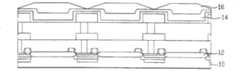
图1为示出根据本发明的图像传感器的纵向结构的剖视图;1 is a cross-sectional view showing a longitudinal structure of an image sensor according to the present invention;
图2A-2C为示出根据本发明的图像传感器的纵向结构的剖视图,分别示出了遮光层、平坦化层、以及滤色器层的构造。2A-2C are cross-sectional views showing the longitudinal structure of an image sensor according to the present invention, respectively showing the configurations of a light-shielding layer, a planarization layer, and a color filter layer.
具体实施方式Detailed ways
下面将详细说明本发明的实施例,其实例示于附图中。尽可能地,在所有附图中,用相同的标号表示相同或相近似的部件。DETAILED DESCRIPTION OF THE INVENTION Embodiments of the invention will be described in detail below, examples of which are illustrated in the accompanying drawings. Wherever possible, the same reference numbers will be used throughout the drawings to refer to the same or like parts.
参见图1,示出了根据本发明的图像传感器的纵向结构,光电二极管12形成于硅衬底10的预定表面上,滤色器层16形成于具有良好透明性的有机材料的平坦化层14上,该滤色器层具有多个滤色器、每个滤色器都具有凸结构。平坦化层14形成于图像传感器的上部,并具有与光电二极管12相对应的凹部。多个微透镜18形成于滤色器层16上,与多个滤色器相对应,以保持滤色器层的总体轮廓,并保护滤色器层的滤色器。Referring to FIG. 1, a vertical structure of an image sensor according to the present invention is shown, a
如图2A所示,其示出了根据本发明的图像传感器的纵向结构,光电二极管12形成为硅衬底10的预定表面区域上的子层。本发明的图像传感器形成于硅衬底上,既可作为CCD型图像传感器又可作为CMOS型图像传感器,包括金属层15,除建立必要的布线连接外,作为遮光层,防止光进入硅衬底的没有被光电二极管覆盖的部分。遮光层15根据填充系数成形,从而具有最小的线宽(linewidth),其根据微透镜的焦距,在光线跟踪(ray tracing)时提供很小的正常金属屏蔽效应。As shown in FIG. 2A , which shows the vertical structure of an image sensor according to the present invention, a
如图2B所示,形成平坦化层14,以改善要在其上形成的滤色器层16的轮廓和均匀性。平坦化层14由具有良好填充系数的旋涂玻璃(spin-on-glass)形成,以有效地减小由遮光层15产生的表面阶梯(vertical differential,也称垂直差异)。除了通过可见波长的光外,平坦化层还用来钝化遮光层15的金属。As shown in FIG. 2B, the
如图2C所示,滤色器层16的滤色器形成在平坦化层14上,用于例如由可选地执行三次的光刻工艺的每个像素,以分别形成滤色器层16的分色层,即,红色滤色器阵列、绿色滤色器阵列、以及蓝色滤色器阵列。滤色器层16要求与多像素系统一致的精确图样及单位像素的微型化。在滤色器层内通过颜料扩散(pigmentdispersing)法难以形成精确的滤色器图样,这是因为颜料已呈现在光刻胶上,还因为这种方法的制造成本在用于较高的分辨率时增加。滤色器层的滤色器的阶梯差异(step differential)可以基于与用于填充间隙的旋涂玻璃的使用相关的填充系数来调节。这影响到微透镜的尺寸和曲率。如果用于微透镜的光刻胶是旋涂的,以致阶梯差异在滤色器层中产生,取决于子层的阶梯尺寸,自对准微透镜可以不用蚀刻和显影工艺来形成。As shown in FIG. 2C , the color filters of the
如上所述,不需要单独的外涂层(overcoat layer)来对准滤色器层上的微透镜,而且由于微透镜是自对准的,所以可以减少工序数。因此,通过采用根据本发明的这种图像传感器及其制造方法,滤色器层的滤色器能够更稳定和更方便地形成,用于每个像素以获得更清晰的图像。在形成滤色器层时,平坦化层被简化并提高了滤色器构造的效率。由于不需要外涂层以及透镜是自对准的,所以光刻工艺也被简化并稳定化。这就降低了制造成本,提升了最终产品的质量,有利于下一代产品的开发与应用。当使用了微透镜的整个表面区域时,改善了光敏度,其又改善了图像特性及传感器质量。As described above, no separate overcoat layer is required to align the microlenses on the color filter layer, and since the microlenses are self-aligned, the number of process steps can be reduced. Therefore, by employing such an image sensor and its manufacturing method according to the present invention, the color filter of the color filter layer can be formed more stably and more conveniently for each pixel to obtain a clearer image. When forming the color filter layer, the planarization layer is simplified and improves the efficiency of the color filter construction. The photolithography process is also simplified and stabilized since no overcoat is required and the lenses are self-aligning. This reduces manufacturing costs, improves the quality of final products, and is conducive to the development and application of next-generation products. When the entire surface area of the microlens is used, light sensitivity is improved, which in turn improves image characteristics and sensor quality.
可以理解,尽管本发明已经参照附图和优选实施例进行了说明,但显然,对于本领域的技术人员来说,在不背离本发明的精神和范围的前提下,可以对本发明作出各种更改和变化。因此,本发明的各种更改、变化由所附的权利要求书及其等同物的内容涵盖。It will be appreciated that although the present invention has been described with reference to the accompanying drawings and preferred embodiments, it will be apparent to those skilled in the art that various changes may be made to the present invention without departing from the spirit and scope of the present invention. and change. Therefore, various modifications and changes of the present invention are covered by the appended claims and their equivalents.
Claims (6)
Applications Claiming Priority (3)
| Application Number | Priority Date | Filing Date | Title |
|---|---|---|---|
| KR1020040116514AKR100628233B1 (en) | 2004-12-30 | 2004-12-30 | Image sensor with automatically arranged microlens and manufacturing method thereof |
| KR10-2004-0116514 | 2004-12-30 | ||
| KR1020040116514 | 2004-12-30 |
Publications (2)
| Publication Number | Publication Date |
|---|---|
| CN1797778A CN1797778A (en) | 2006-07-05 |
| CN100429779Ctrue CN100429779C (en) | 2008-10-29 |
Family
ID=36639308
Family Applications (1)
| Application Number | Title | Priority Date | Filing Date |
|---|---|---|---|
| CNB2005101257729AExpired - Fee RelatedCN100429779C (en) | 2004-12-30 | 2005-12-01 | Image sensor and manufacturing method thereof |
Country Status (3)
| Country | Link |
|---|---|
| US (1) | US7414232B2 (en) |
| KR (1) | KR100628233B1 (en) |
| CN (1) | CN100429779C (en) |
Families Citing this family (9)
| Publication number | Priority date | Publication date | Assignee | Title |
|---|---|---|---|---|
| JO2803B1 (en)* | 2006-05-10 | 2014-03-15 | كراون باكيجنج تكنولوجي،انك. | Opening Device |
| US7593248B2 (en) | 2006-11-16 | 2009-09-22 | Aptina Imaging Corporation | Method, apparatus and system providing a one-time programmable memory device |
| US20080117661A1 (en)* | 2006-11-16 | 2008-05-22 | Micron Technology, Inc. | Method, apparatus and system providing memory cells associated with a pixel array |
| US7875840B2 (en)* | 2006-11-16 | 2011-01-25 | Aptina Imaging Corporation | Imager device with anti-fuse pixels and recessed color filter array |
| KR101441133B1 (en)* | 2008-03-26 | 2014-09-17 | 엘지전자 주식회사 | How to control the drawer drive of refrigerator |
| CN101588506B (en)* | 2008-05-22 | 2012-05-30 | 索尼株式会社 | Solid-state imaging device, manufacturing method thereof, and electronic device |
| US8324701B2 (en)* | 2010-07-16 | 2012-12-04 | Visera Technologies Company Limited | Image sensors |
| US10355172B1 (en)* | 2018-04-10 | 2019-07-16 | Nthdegree Technologies Worldwide Inc. | Self-alignment of optical structures to random array of printed micro-LEDs |
| CN110544700B (en)* | 2019-08-19 | 2022-01-04 | 上海集成电路研发中心有限公司 | Micro-lens array integrated in image sensor and preparation method thereof |
Citations (5)
| Publication number | Priority date | Publication date | Assignee | Title |
|---|---|---|---|---|
| JPH06236979A (en)* | 1993-02-12 | 1994-08-23 | Matsushita Electron Corp | Solid-state image pick-up device |
| US5739548A (en)* | 1995-05-02 | 1998-04-14 | Matsushita Electronics Corporation | Solid state imaging device having a flattening layer and optical lenses |
| KR20000044582A (en)* | 1998-12-30 | 2000-07-15 | 김영환 | Image sensor |
| US20040084700A1 (en)* | 2000-08-31 | 2004-05-06 | Chae-Sung Kim | Image sensor and method for fabricating the same |
| CN1518119A (en)* | 2003-01-16 | 2004-08-04 | ���ǵ�����ʽ���� | Structure of Complementary Metal Oxide Semiconductor Image Sensing Device and Manufacturing Method |
Family Cites Families (3)
| Publication number | Priority date | Publication date | Assignee | Title |
|---|---|---|---|---|
| JPS59198754A (en)* | 1983-04-26 | 1984-11-10 | Toshiba Corp | Color solid-state imaging device |
| US6297540B1 (en)* | 1999-06-03 | 2001-10-02 | Intel Corporation | Microlens for surface mount products |
| US20050224694A1 (en)* | 2004-04-08 | 2005-10-13 | Taiwan Semiconductor Manufacturing Co. Ltd. | High efficiency microlens array |
- 2004
- 2004-12-30KRKR1020040116514Apatent/KR100628233B1/ennot_activeExpired - Fee Related
- 2005
- 2005-12-01CNCNB2005101257729Apatent/CN100429779C/ennot_activeExpired - Fee Related
- 2005-12-05USUS11/293,080patent/US7414232B2/ennot_activeExpired - Fee Related
Patent Citations (5)
| Publication number | Priority date | Publication date | Assignee | Title |
|---|---|---|---|---|
| JPH06236979A (en)* | 1993-02-12 | 1994-08-23 | Matsushita Electron Corp | Solid-state image pick-up device |
| US5739548A (en)* | 1995-05-02 | 1998-04-14 | Matsushita Electronics Corporation | Solid state imaging device having a flattening layer and optical lenses |
| KR20000044582A (en)* | 1998-12-30 | 2000-07-15 | 김영환 | Image sensor |
| US20040084700A1 (en)* | 2000-08-31 | 2004-05-06 | Chae-Sung Kim | Image sensor and method for fabricating the same |
| CN1518119A (en)* | 2003-01-16 | 2004-08-04 | ���ǵ�����ʽ���� | Structure of Complementary Metal Oxide Semiconductor Image Sensing Device and Manufacturing Method |
Also Published As
| Publication number | Publication date |
|---|---|
| US7414232B2 (en) | 2008-08-19 |
| US20060145055A1 (en) | 2006-07-06 |
| CN1797778A (en) | 2006-07-05 |
| KR100628233B1 (en) | 2006-09-26 |
| KR20060077610A (en) | 2006-07-05 |
Similar Documents
| Publication | Publication Date | Title |
|---|---|---|
| KR100654143B1 (en) | Solid-state imaging device, method for manufacturing solid-state imaging device, camera | |
| US7427799B2 (en) | Complementary metal oxide semiconductor image sensor and method for fabricating the same | |
| KR100857305B1 (en) | Lens array and method of making same | |
| US7750360B2 (en) | Solid-state image pickup device | |
| US20090278220A1 (en) | Image sensor and fabricting method thereof | |
| US20060146412A1 (en) | Image sensor having square microlens | |
| US20060138497A1 (en) | CMOS image sensor and method for fabricating the same | |
| US7339155B2 (en) | CMOS image sensor and method for fabricating the same | |
| US7078258B2 (en) | Image sensor and manufacturing method of image sensor | |
| CN100429779C (en) | Image sensor and manufacturing method thereof | |
| US7579625B2 (en) | CMOS image sensor and method for manufacturing the same | |
| US7535043B2 (en) | Solid-state image sensor, method of manufacturing the same, and camera | |
| CN101183663B (en) | Image sensor and manufacturing method thereof | |
| US20070102716A1 (en) | Image sensor and fabricating method thereof | |
| JP2011243749A (en) | Solid state image pickup device and manufacturing method thereof | |
| US20060145056A1 (en) | Image sensor having diffractive lens and method for fabricating the same | |
| US20080048284A1 (en) | Image sensor and fabrication method thereof | |
| US20060138487A1 (en) | CMOS image sensor and method for fabricating the same | |
| US20060125020A1 (en) | CMOS image sensor and method for fabricating the same | |
| KR20010061586A (en) | Method for fabricating microlens in image sensor | |
| KR100886567B1 (en) | Mask for forming micro lens pattern of image sensor | |
| KR100628230B1 (en) | Image sensor having inclined color filter and its manufacturing method | |
| US20070145238A1 (en) | Method for Manufacturing Mask and CMOS Image Sensor | |
| JP2011165791A (en) | Solid-state imaging element, and method of manufacturing the same | |
| KR940004300B1 (en) | Color filter and its manufacturing method |
Legal Events
| Date | Code | Title | Description |
|---|---|---|---|
| C06 | Publication | ||
| PB01 | Publication | ||
| C10 | Entry into substantive examination | ||
| SE01 | Entry into force of request for substantive examination | ||
| C14 | Grant of patent or utility model | ||
| GR01 | Patent grant | ||
| C17 | Cessation of patent right | ||
| CF01 | Termination of patent right due to non-payment of annual fee | Granted publication date:20081029 Termination date:20131201 |